2.0w audio power amplifier ce0031series introduction … · watt of continuous average power to a...
TRANSCRIPT
V1.1 1(13)
2.0W Audio Power Amplifier CE0031Series
CE0031①②③
INTRODUCTION
The CE0031 is audio amplifiers designed
for portable communication device
applications.It is capable of delivering 1.6
watt of continuous average power to a 4Ω
BTL load with less than 1% distortion
(THD+N) from a 5V power system.
FEATURES
Wide operation Range 2.0~6.8V
Low Distortion:THD+N=0.15%(Typ.)
(For VDD=5.0V,RL=4.0Ω,Pout=0.63W)
Low Distortion:THD+N=1%(Typ.)
(For VDD=5.0V,RL=4.0Ω,Pout=1.6W)
Low Shutdown Current:1.0uA
Minimize the turn-on and turn-off pop noise
Thermal Shutdown Protection
Over Current Protection
APPLICATIONS
Wireless handsets
Portable audio devices
PDAs, Notebook computer
ORDER INFORMATION:
DESIGNATOR SYMBOL DESCRIPTION
① A Standard
② H CE High Active
③ S Package:SOP8
SM Package:MSOP8
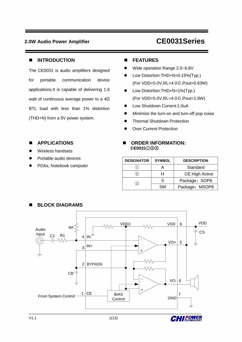
BLOCK DIAGRAMS
Audio
Input C1 R1
RF
CB
From System Control
4
3
2
1 CE
BYPASS
IN+
IN-
VDD2
BIAS
Control
-
+
-
+
VDD
VO+
VO-
GND
6
5
8
7
VDD
CS
2.0W Audio Power Amplifier
CE0031Series
V1.1 2(13)
2.0W Audio Power Amplifier CE0031Series
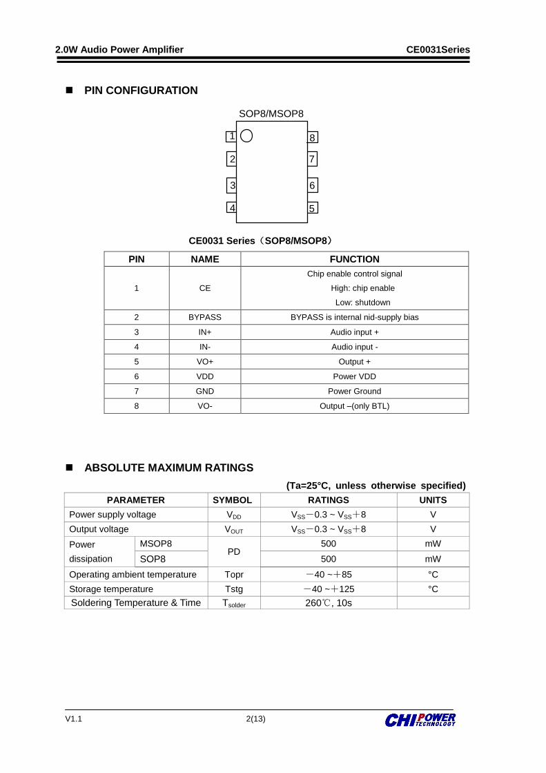
PIN CONFIGURATION
81
2
3
4 5
6
7
SOP8/MSOP8
CE0031 Series(SOP8/MSOP8)
PIN NAME FUNCTION
1 CE
Chip enable control signal
High: chip enable
Low: shutdown
2 BYPASS BYPASS is internal nid-supply bias
3 IN+ Audio input +
4 IN- Audio input -
5 VO+ Output +
6 VDD Power VDD
7 GND Power Ground
8 VO- Output –(only BTL)
ABSOLUTE MAXIMUM RATINGS
(Ta=25°C, unless otherwise specified)
PARAMETER SYMBOL RATINGS UNITS
Power supply voltage VDD VSS-0.3 ~ VSS+8 V
Output voltage VOUT VSS-0.3 ~ VSS+8 V
Power
dissipation
MSOP8 PD
500 mW
SOP8 500 mW
Operating ambient temperature Topr -40 ~+85 °C
Storage temperature Tstg -40 ~+125 °C
Soldering Temperature & Time Tsolder 260℃, 10s

V1.1 3(13)
2.0W Audio Power Amplifier CE0031Series
ELECTRICAL CHARACTERISTICS
(Ta=25°C, unless otherwise specified)
PARAMETER SYMBOL CONDITIONS MIN TYP MAX UNITS
Operation Voltage VDD 2.0 6.8 V
Shutdown Current Ioff CE=GND 1.0 uA
Operating Current Iss VDD=5V,CE=VDD,No Load 3.0 mA
BYPASS Voltage VBYPASS VDD=5V,CE=VDD VDD/2 V
Total Harmonic Distortion
+ Noise THD+N
VDD=5.0V,RL=4Ω ,POUT=0.63W 0.15 %
VDD=5.0V,RL=8Ω ,POUT=0.63W 0.15 %
Output Offset Voltage VOS VIN=0V 30 mV
POWER Rehection Ratio PSRR f=1KHz 70 dB
Enable Time TON VDD=5V,CB=1uF 70 mS
Shutdown Time TOFF VDD=5V,CB=1uF 70 mS
Current Limitation ILMT VDD=5V 850 mA

V1.1 4(13)
2.0W Audio Power Amplifier CE0031Series
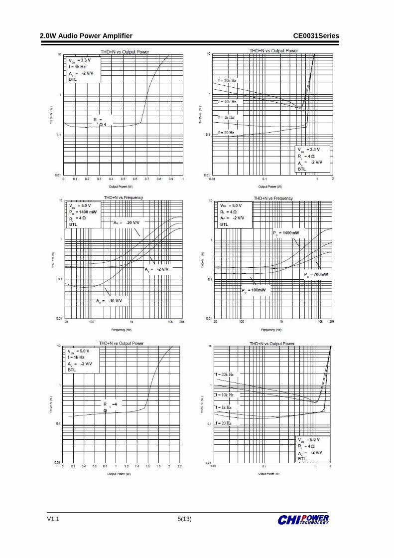
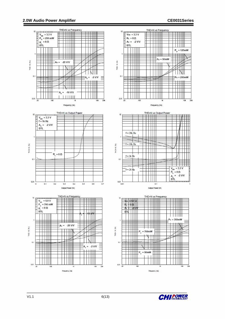
TYPICAL PERFORMANCE CHARACTERISTICS
V1.1 5(13)
2.0W Audio Power Amplifier CE0031Series
V1.1 6(13)
2.0W Audio Power Amplifier CE0031Series

V1.1 7(13)
2.0W Audio Power Amplifier CE0031Series

V1.1 8(13)
2.0W Audio Power Amplifier CE0031Series

V1.1 9(13)
2.0W Audio Power Amplifier CE0031Series

V1.1 10(13)
2.0W Audio Power Amplifier CE0031Series
V1.1 11(13)
2.0W Audio Power Amplifier CE0031Series
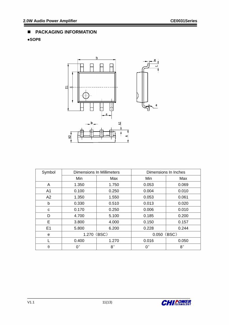
PACKAGING INFORMATION
●SOP8
Symbol Dimensions In Millimeters Dimensions In Inches
Min Max Min Max
A 1.350 1.750 0.053 0.069
A1 0.100 0.250 0.004 0.010
A2 1.350 1.550 0.053 0.061
b 0.330 0.510 0.013 0.020
c 0.170 0.250 0.006 0.010
D 4.700 5.100 0.185 0.200
E 3.800 4.000 0.150 0.157
E1 5.800 6.200 0.228 0.244
e 1.270(BSC) 0.050(BSC)
L 0.400 1.270 0.016 0.050
θ 0° 8° 0° 8°

V1.1 12(13)
2.0W Audio Power Amplifier CE0031Series
● MSOP8
Symbol Dimensions In Millimeters Dimensions In Inches
Min Max Min Max
A 0.820 1.100 0.032 0.043
A1 0.020 0.150 0.001 0.006
A2 0.750 0.950 0.030 0.037
b 0.250 0.380 0.010 0.015
c 0.090 0.230 0.004 0.009
D 2.900 3.100 0.114 0.122
e 0.650(BSC) 0.026(BSC)
E 2.900 3.100 0.114 0.122
E1 4.750 5.050 0.187 0.199
L 0.400 0.800 0.016 0.031
θ 0° 6° 0° 6°
V1.1 13(13)
2.0W Audio Power Amplifier CE0031Series
© Nanjing Chipower Electronics Inc.
Chipower cannot assume responsibility for use of any circuitry other than circuitry entirely embodied in a
Chipower product. No circuit patent license, copyrights or other intellectual property rights are implied.
Chipower reserves the right to make changes to their products or specifications without notice. Customers
are advised to obtain the latest version of relevant information to verify, before placing orders, that
information being relied on is current and complete.