4 x 6w power amplifier for car radio - bdtictda7372b 4 x 6w power amplifier for car radio high power...
TRANSCRIPT
TDA7372B
4 x 6W POWER AMPLIFIER FOR CAR RADIO
HIGH POWER CAPABILITY:4x6W min/4Ω @14.4V, 1KHz, 10%4x10W typ/2Ω @14.4V, 1KHz, 10%MINIMUM EXTERNAL COMPONENT COUNT- INTERNALLY FIXED GAIN (40dB)- NO BOOTSTRAP CAPACITORS- NO EXTERNAL COMPENSATIONST-BY FUNCTION (CMOS COMPATIBLE)MUTE FUNCTION (CMOS COMPATIBLE)NO AUDIBLE POP DURING MUTE/ST-BYOPERATIONSLOW SUPPLY SELF MUTINGPROGRAMMABLE TURN ON DELAY
PROTECTIONS:
AC OUTPUT SHORT CIRCUIT TO GNDDC OUTPUT SHORT CIRCUIT TO GND ANDTO VS AT POWER ONSOFT THERMAL LIMITEROVERRATING CHIP TEMPERATURELOAD DUMP VOLTAGE
FORTUITOUS OPEN GNDREVERSE BATTERYESD PROTECTION
DESCRIPTIONThe TDA7372B is a new technology class AB quadchannels Audio Power Amplifier in Multiwatt15package designed for car radio applications.Thanks to the fully complementary PNP/NPN out-put configuration the TDA7372B delivers a rail torail voltage swing with no need of boostrap capacitors.
September 2003
®
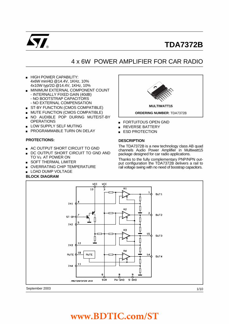
BLOCK DIAGRAM
MULTIWATT15
ORDERING NUMBER: TDA7372B
1/10
www.BDTIC.com/ST

PIN CONNECTION (Top view)
ABSOLUTE MAXIMUM RATINGS
Symbol Parameter Value Unit
VS DC Supply Voltage 28 V
VOP Operating Supply Voltage 18 V
VPEAK Peak Supply Voltage (t = 50ms) 50 V
IO Output Peak Current (not rep. t = 100µs) 4 A
IO Output Peak Current (rep. f > 10Hz) 3 A
Ptot Power Dissipation (Tcase = 85°C) 32 W
Tstg, Tj Storage and Junction Temperature -40 to 150 °C
THERMAL DATA
Symbol Description Value Unit
Rth j-case Thermal Resistance Junction-case Max 2 °C/W
TDA7372B
2/10
www.BDTIC.com/ST

ELECTRICAL CHARACTERISTICS (Refer to the test circuit; VS = 14.4V; RL = 4Ω, Tamb = 25°C, f = 1kHz, unless otherwise specified)
Symbol Parameter Test Condition Min. Typ. Max. UnitVS Supply Range 8 18 VId Total Quiescent Drain Current 150 mA
PO Output Power RL = 4Ω; THD = 10%each channel
6 6.5 W
RL = 2Ω; THD = 10%each channel
10 W
d Distortion RL = 4Ω;PO = 0.1 to 3W
0.08 0.5 %
CT Cross Talk f = 1kHz; Rg = 0f = 10kHz; Rg = 0
45 5040
dBdB
RIN Input Impedance 35 KΩGV Voltage Gain 40 dBGV Voltage Gain Match. 1 dBBW Bandwidth @ -3dB 75 KHzENO Output Noise Voltage (*) Rg = 0 300 µVSVR Supply Voltage Rejection Rg = 0; f = 100Hz 45 dBASB Stand-by Attenuation 80 dBISB ST-BY Current Consumption Vpin7 = 1.5V 100 µA
IPIN 7 ST-BY Pin Current Play mode; Vpin7 = 5V 50 µAOutput Under Short (Maxdriving current under fault)
5 mA
VSB IN ST-BY IN Threshold Voltage 1.5 VVSB OUT ST-BY OUT Threshold Voltage 3.5 V
AM MUTE Attenuation 80 dBVM IN MUTE IN Threshold Voltage 1.5 V
VM OUT MUTE OUT Threshold Voltage 3.5 V
(*) 22Hz to 22KHz
TDA7372B
3/10
www.BDTIC.com/ST

TEST AND APPLICATION CIRCUIT
Figure 1: P.C. Board and components layout of the Test and Application Circuit (1:1 scale)
If high source resistance is present (e.g. passive audio controls) it might be necessary to add C = 470pF from each input pin to S-GND toprevent instability phenomena.
10µFC13
R2
TDA7372B
4/10
www.BDTIC.com/ST

Figure 2: Quiescent Drain Current vs. SupplyVoltage
Figure 4: Output Power vs Supply Voltage
Figure 6: Distortion vs. Output Power
Figure 3: Output Power vs. Supply Voltage
Figure 5: Output power vs. Frequency vs.COUTValue
Figure 7: Distortion vs. Output Power
TDA7372B
5/10
www.BDTIC.com/ST

Figure 8: Distortion vs. Frequency
Figure 10: Cross-Talk vs. Frequency
Figure 12: Total Power Dissipation and Efficiency
Figure 9: Distortion vs. Frequency
Figure 11: Supply Voltage Rejection vs. Frequency
Figure 13: Total Power Dissipation and Efficiencyvs. Output Power
Ptot (W) Ptot (W)
Ptot
Ptot
TDA7372B
6/10
www.BDTIC.com/ST
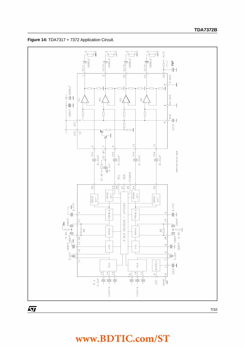
Figure 14: TDA7317 + 7372 Application Circuit.
10µF
TDA7372B
7/10
www.BDTIC.com/ST

FUNCTIONAL DESCRIPTION
Function Description
GENERAL
The TDA7372B is a quad channel single package audio power amplifier intended to reduce themismatch in the electrical characteristics among the four different channels and to consistentlydrop the external component count. It contains four non inverting stages whose gain isinternally fixed to 40dB.
OUTPUT STAGE
The output stage is a single ended type suitable to drine 4Ω loads. It consists of a class AB fullycomplementary PNP/NPN stages short circuit protected.A rail to rail output swing is achieved without need of boostrap capacitors. Moreover, theexternal compensation is not necessary.
ST-BYThe device features a St-BY function which shuts down the internal bias supplies when the ST-BY input is low. In ST-BY mode the amplifier sinks a small current (in the range of few µAs).When the St-BY pin is high the IC becomes fully operational.
MUTE
A mute function is also provided. This reduces the gain of the input stage to a level effectivelyeliminating any audio input influence on the output stage when the mute line is low. When themute line is high the normal input path is restored.The device goes automatically is mute status when the supply voltage goes below the minimumallowed value. This prevents pop noises whenever the battery voltage drops below a fixedthreshold. When the supply voltage rises to its nominal value the device recovers the playcondition with a delay fixed by the CSVR capacitor.
THERMALPROTECTION
The Thermal protection principle involves two different stepsa) Soft thermal limitationb) ShutdownUntil the juntion temperature remains below a preset threshold, the I.C. will deliver the fullpower. Once the threshold has been reached, the device automatically goes, into mute status.The play to mute transition is internally controlled so producing a soft muting without unpleasenteffect. Supposing the junction temperature does not reduce to safe levels a complete shutdownwill occur.
BUILT-IN SHORTCIRCUIT
PROTECTION
Reliable and safe operation in presence of:- AC short circuit to GND- DC short circuit to GND and to VS during power-on phaseis assured by a built-in protection circuitry.the DC short protector acts in such a way to avoid the device is turned on (by ST-BY) when aDC short is present between out to GND or out to VS. Due to this reason it is necessary tointroduce a proper delay on the st-by pin (expecially when it is driven by VS.)More over, as the involved circuitry is normally disabled when a current higher than 5mA isflowing into the st-by pin, it is important, in order not to disable it, to have the external currentsource driving the pin it self limited to 5mA. (figure 1 is showing relevant waveforms).
Figure 15: Fault (DC short) waveforms
TDA7372B
8/10
www.BDTIC.com/ST

Multiwatt15 V
DIM.mm inch
MIN. TYP. MAX. MIN. TYP. MAX.
A 5 0.197
B 2.65 0.104
C 1.6 0.063
D 1 0.039
E 0.49 0.55 0.019 0.022
F 0.66 0.75 0.026 0.030
G 1.02 1.27 1.52 0.040 0.050 0.060
G1 17.53 17.78 18.03 0.690 0.700 0.710
H1 19.6 0.772
H2 20.2 0.795
L 21.9 22.2 22.5 0.862 0.874 0.886
L1 21.7 22.1 22.5 0.854 0.870 0.886
L2 17.65 18.1 0.695 0.713
L3 17.25 17.5 17.75 0.679 0.689 0.699
L4 10.3 10.7 10.9 0.406 0.421 0.429
L7 2.65 2.9 0.104 0.114
M 4.25 4.55 4.85 0.167 0.179 0.191
M1 4.63 5.08 5.53 0.182 0.200 0.218
S 1.9 2.6 0.075 0.102
S1 1.9 2.6 0.075 0.102
Dia1 3.65 3.85 0.144 0.152
OUTLINE ANDMECHANICAL DATA
TDA7372B
9/10
www.BDTIC.com/ST

Information furnished is believed to be accurate and reliable. However, STMicroelectronics assumes no responsibility for the consequencesof use of such information nor for any infringement of patents or other rights of third parties which may result from its use. No license isgranted by implication or otherwise under any patent or patent rights of STMicroelectronics. Specifications mentioned in this publication aresubject to change without notice. This publication supersedes and replaces all information previously supplied. STMicroelectronics productsare not authorized for use as critical components in life support devices or systems without express written approval of STMicroelectronics.
The ST logo is a registered trademark of STMicroelectronics.All other names are the property of their respective owners
© 2003 STMicroelectronics - All rights reserved
STMicroelectronics GROUP OF COMPANIESAustralia – Belgium - Brazil - Canada - China – Czech Republic - Finland - France - Germany - Hong Kong - India - Israel - Italy - Japan -
Malaysia - Malta - Morocco - Singapore - Spain - Sweden - Switzerland - United Kingdom - United Stateswww.st.com
TDA7372B
10/10
www.BDTIC.com/ST