verilog review - cornell university · 2015-10-14 · • behavioral verilog – gate level –...
TRANSCRIPT

Verilog Review
ECE 4750 Computer Architecture Christopher Batten
FA FA FA FA module adder( input [3:0] A, B, output cout, output [3:0] S );
wire c0, c1, c2; FA fa0( A[0], B[0], 1�b0, c0, S[0] ); FA fa1( A[1], B[1], c0, c1, S[1] ); FA fa2( A[2], B[2], c1, c2, S[2] ); FA fa3( A[3], B[3], c2, cout, S[3] );
endmodule

ECE 4750 Computer Architecture • Verilog Review • 2
FA FA FA FA
module adder( input [3:0] A, B, output cout, output [3:0] S );
wire c0, c1, c2; FA fa0( A[0], B[0], 1�b0, c0, S[0] ); FA fa1( A[1], B[1], c0, c1, S[1] ); FA fa2( A[2], B[2], c1, c2, S[2] ); FA fa3( A[3], B[3], c2, cout, S[3] );
endmodule
Verilog Review • Data types • Structural Verilog • Behavioral Verilog
– Gate level – Register transfer level – Functional level
• Parameterized Static Elaboration
• Greatest Common Divisor

ECE 4750 Computer Architecture • Verilog Review • 3
Primary Verilog data type is a bit-vector where bits can take on one of four values
Value Meaning 0 Logic zero 1 Logic one X Unknown logic value Z High impedance, floating
An X bit might be a 0, 1, Z, or in transition. We can set bits to be X in situations where we don�t care what the value is. This can help catch bugs and
improve synthesis quality.

ECE 4750 Computer Architecture • Verilog Review • 4
The Verilog keyword wire is used to denote a standard hardware net
wire [15:0] instruction; wire [15:0] memory_req; wire [ 7:0] small_net;
inst
ruct
ion
mem
ory_
req
inst
ruct
ion
smal
l_ne
t
?
Absolutely no type safety when connecting nets!

ECE 4750 Computer Architecture • Verilog Review • 5
Verilog includes ways to specify bit literals in various bases
• Binary literals – 8�b0000_0000 – 8�b0xx0_1xx1
• Hexadecimal literals – 32�h0a34_def1 – 16�haxxx
• Decimal literals – 32�d42
4�b10_11 Underscores are ignored
Base format (d,b,o,h)
Decimal number representing size in bits
We’ll learn how to actually assign literals to
nets a little later

ECE 4750 Computer Architecture • Verilog Review • 6
FA FA FA FA
module adder( input [3:0] A, B, output cout, output [3:0] S );
wire c0, c1, c2; FA fa0( A[0], B[0], 1�b0, c0, S[0] ); FA fa1( A[1], B[1], c0, c1, S[1] ); FA fa2( A[2], B[2], c1, c2, S[2] ); FA fa3( A[3], B[3], c2, cout, S[3] );
endmodule
Verilog Review • Data types • Structural Verilog • Behavioral Verilog
– Gate level – Register transfer level – Functional level
• Parameterized Static Elaboration
• Greatest Common Divisor
ECE 4750 Computer Architecture • Verilog Review • 7
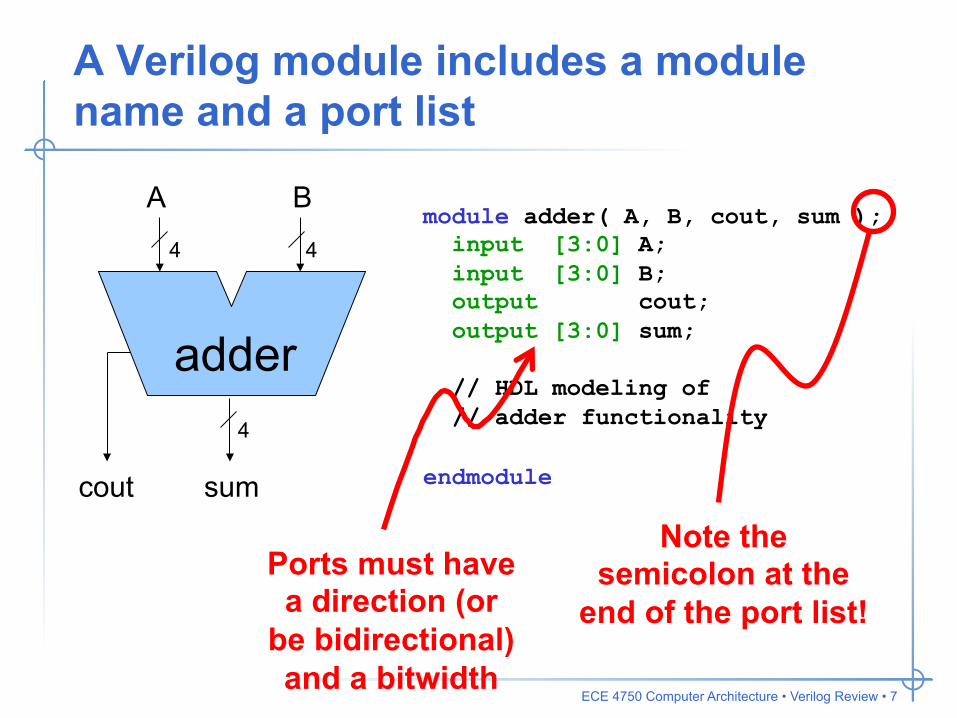
A Verilog module includes a module name and a port list
adder
A B
sum cout
module adder( A, B, cout, sum ); input [3:0] A; input [3:0] B; output cout; output [3:0] sum; // HDL modeling of // adder functionality endmodule
Note the semicolon at the
end of the port list! Ports must have
a direction (or be bidirectional) and a bitwidth
4 4
4

ECE 4750 Computer Architecture • Verilog Review • 8
Traditional Verilog-1995 Syntax
module adder( A, B, cout, sum ); input [3:0] A; input [3:0] B; output cout; output [3:0] sum;
ANSI C Style Verilog-2001 Syntax
module adder( input [3:0] A, input [3:0] B, output cout, output [3:0] sum );
A Verilog module includes a module name and a port list
adder
A B
sum cout
4 4
4

ECE 4750 Computer Architecture • Verilog Review • 9
A module can instantiate other modules creating a module hierarchy
module FA( input a, b, cin output cout, sum ); // HDL modeling of 1 bit // adder functionality endmodule
FA
b a
c
cin
cout

ECE 4750 Computer Architecture • Verilog Review • 10
A module can instantiate other modules creating a module hierarchy
adder
A B
S cout
FA FA FA FA
module adder( input [3:0] A, B, output cout, output [3:0] S );
wire c0, c1, c2; FA fa0( ... ); FA fa1( ... ); FA fa2( ... ); FA fa3( ... );
endmodule

ECE 4750 Computer Architecture • Verilog Review • 11
A module can instantiate other modules creating a module hierarchy
adder
A B
S cout
FA FA FA FA
module adder( input [3:0] A, B, output cout, output [3:0] S );
wire c0, c1, c2; FA fa0( A[0], B[0], 1�b0, c0, S[0] ); FA fa1( A[1], B[1], c0, c1, S[1] ); FA fa2( A[2], B[2], c1, c2, S[2] ); FA fa3( A[3], B[3], c2, cout, S[3] );
endmodule Carry Chain

ECE 4750 Computer Architecture • Verilog Review • 12
Verilog supports connecting ports by position and by name
Connecting ports by ordered list FA fa0( A[0], B[0], 1�b0, c0, S[0] );
Connecting ports by name (compact) FA fa0( .a(A[0]), .b(B[0]), .cin(1�b0), .cout(c0), .sum(S[0]) );
Connecting ports by name FA fa0 ( .a (A[0]), .b (B[0]), .cin (1�b0), .cout (c0), .sum (S[0]) );
For all but the smallest modules, connecting ports by name yields clearer and
less buggy code.

ECE 4750 Computer Architecture • Verilog Review • 14
module adder( ... );
endmodule
module adder( input [3:0] A, B, output cout, output [3:0] S );
endmodule
Let’s review how to turn our schematic diagram into structural Verilog
module adder( input [3:0] A, B, output cout, output [3:0] S );
FA fa0( ... ); FA fa1( ... ); FA fa2( ... ); FA fa3( ... );
endmodule
FA FA FA FA
module adder( input [3:0] A, B, output cout, output [3:0] S );
wire c0, c1, c2; FA fa0( A[0], B[0], 1�b0, c0, S[0] ); FA fa1( A[1], B[1], c0, c1, S[1] ); FA fa2( A[2], B[2], c1, c2, S[2] ); FA fa3( A[3], B[3], c2, cout, S[3] );
endmodule

ECE 4750 Computer Architecture • Verilog Review • 15
FA FA FA FA
module adder( input [3:0] A, B, output cout, output [3:0] S );
wire c0, c1, c2; FA fa0( A[0], B[0], 1�b0, c0, S[0] ); FA fa1( A[1], B[1], c0, c1, S[1] ); FA fa2( A[2], B[2], c1, c2, S[2] ); FA fa3( A[3], B[3], c2, cout, S[3] );
endmodule
Verilog Review • Data types • Structural Verilog • Behavioral Verilog
– Gate level – Register transfer level – Functional level
• Parameterized Static Elaboration
• Greatest Common Divisor
ECE 4750 Computer Architecture • Verilog Review • 16
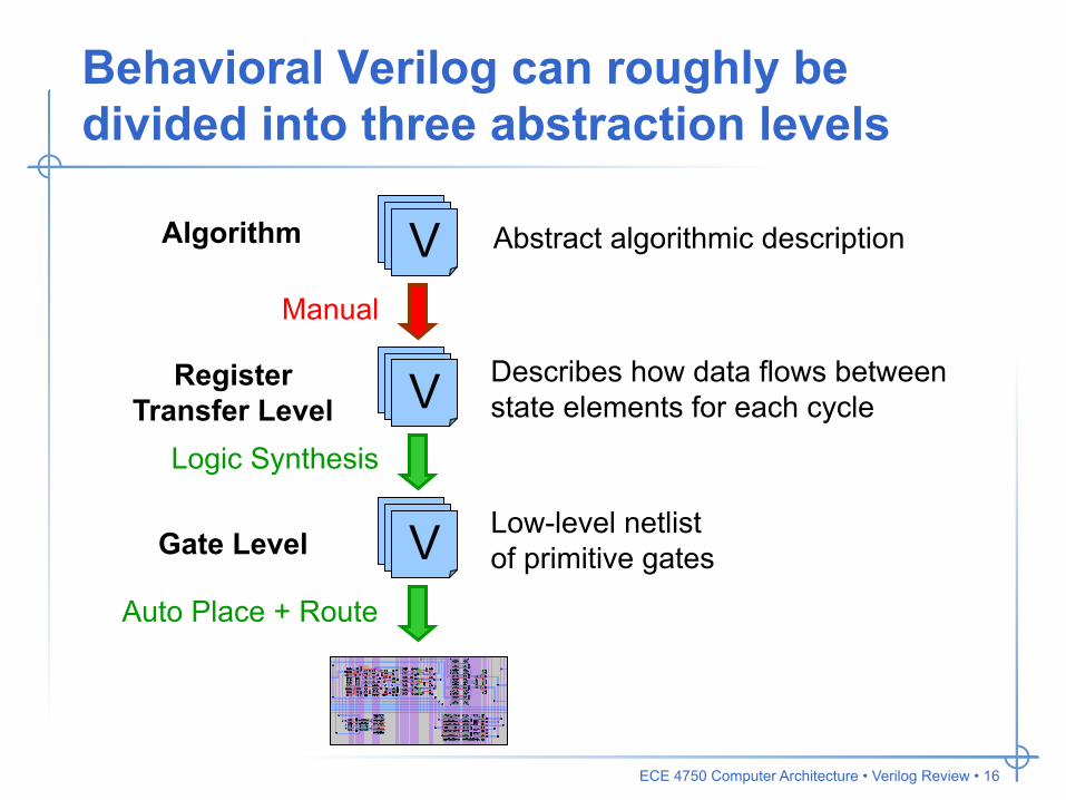
Behavioral Verilog can roughly be divided into three abstraction levels
Algorithm
Register Transfer Level
Gate Level
Manual
Logic Synthesis
Auto Place + Route
V
V
V Abstract algorithmic description
Describes how data flows between state elements for each cycle
Low-level netlist of primitive gates

ECE 4750 Computer Architecture • Verilog Review • 17
module mux4( input a, b, c, d, input [1:0] sel, output out );
wire [1:0] sel_b; not not0( sel_b[0], sel[0] ); not not1( sel_b[1], sel[1] );
wire n0, n1, n2, n3; and and0( n0, c, sel[1] ); and and1( n1, a, sel_b[1] ); and and2( n2, d, sel[1] ); and and3( n3, b, sel_b[1] );
wire x0, x1; nor nor0( x0, n0, n1 ); nor nor1( x1, n2, n3 );
wire y0, y1; or or0( y0, x0, sel[0] ); or or1( y1, x1, sel_b[0] ); nand nand0( out, y0, y1 );
endmodule
Gate-level Verilog uses structural Verilog to connect primitive gates
sel[0] sel[1] c a d b
out

ECE 4750 Computer Architecture • Verilog Review • 18
Continuous assignment statements assign one net to another or to a literal
Explicit continuous assignment wire [15:0] netA; wire [15:0] netB; assign netA = 16�h3333; assign netB = netA; Implicit continuous assignment wire [15:0] netA = 16�h3333; wire [15:0] netB = netA;

ECE 4750 Computer Architecture • Verilog Review • 19
module mux4( input a, b, c, d input [1:0] sel, output out ); wire out, t0, t1; assign out = ~( (t0 | sel[0]) & (t1 | ~sel[0]) ); assign t1 = ~( (sel[1] & d) | (~sel[1] & b) ); assign t0 = ~( (sel[1] & c) | (~sel[1] & a) ); endmodule
Using continuous assignments to implement an RTL four input multiplexer
module mux4( input a, b, c, d input [1:0] sel, output out ); wire t0, t1; assign t0 = ~( (sel[1] & c) | (~sel[1] & a) ); assign t1 = ~( (sel[1] & d) | (~sel[1] & b) ); assign out = ~( (t0 | sel[0]) & (t1 | ~sel[0]) ); endmodule
The order of these continuous assignment statements does not matter.
They essentially happen in parallel!

ECE 4750 Computer Architecture • Verilog Review • 20
Verilog RTL includes many operators in addition to basic boolean logic // Four input multiplexer module mux4( input a, b, c, d input [1:0] sel, output out );
assign out = ( sel == 0 ) ? a : ( sel == 1 ) ? b : ( sel == 2 ) ? c : ( sel == 3 ) ? d : 1�bx;
endmodule // Simple four bit adder module adder( input [3:0] op1, op2, output [3:0] sum );
assign sum = op1 + op2;
endmodule
If input is undefined we want to propagate that
information.

ECE 4750 Computer Architecture • Verilog Review • 21
Verilog RTL operators Arithmetic + - * / % **
Logical ! && ||
Relational > < >= <=
Equality == != === !===
Bitwise ~ & | ^ ^~
wire [ 3:0] net1 = 4�b00xx; wire [ 3:0] net2 = 4�b1110; wire [11:0] net3 = { 4�b0, net1, net2 };
Reduction & ~& | ~| ^ ^~
Shift >> << >>> <<<
Concatenation { }
Conditional ?:
Avoid ( / % ** ) since the usually synthesize poorly
wire equal = ( net3 === 12�b0000_1110_00xx );

ECE 4750 Computer Architecture • Verilog Review • 22
Always blocks have parallel inter-block and sequential intra-block semantics module mux4( input a, b, c, d input [1:0] sel, output out ); reg out, t0, t1; always @( a or b or c or d or sel ) begin t0 = ~( (sel[1] & c) | (~sel[1] & a) ); t1 = ~( (sel[1] & d) | (~sel[1] & b) ); out = ~( (t0 | sel[0]) & (t1 | ~sel[0]) ); end endmodule The always block is reevaluated
whenever a signal in its sensitivity list changes

ECE 4750 Computer Architecture • Verilog Review • 23
Always blocks have parallel inter-block and sequential intra-block semantics module mux4( input a, b, c, d input [1:0] sel, output out ); reg out, t0, t1; always @( a or b or c or d or sel ) begin t0 = ~( (sel[1] & c) | (~sel[1] & a) ); t1 = ~( (sel[1] & d) | (~sel[1] & b) ); out = ~( (t0 | sel[0]) & (t1 | ~sel[0]) ); end endmodule The order of these procedural
assignment statements does matter. They essentially happen in sequentially!
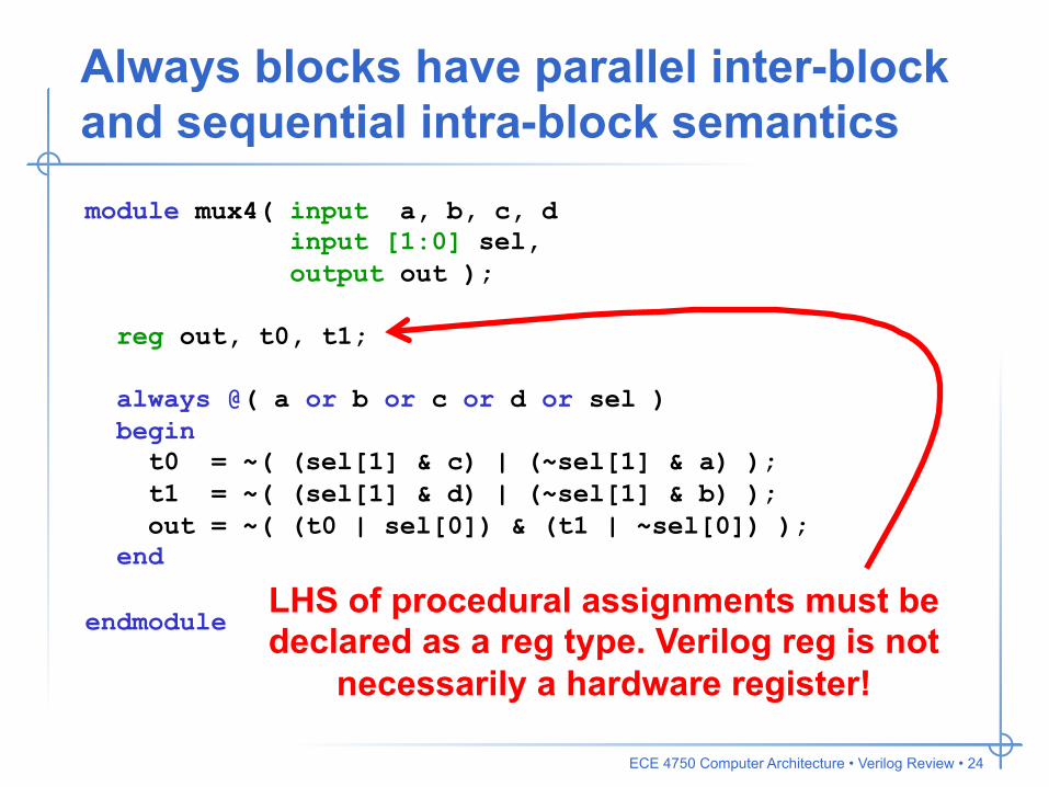
ECE 4750 Computer Architecture • Verilog Review • 24
Always blocks have parallel inter-block and sequential intra-block semantics module mux4( input a, b, c, d input [1:0] sel, output out ); reg out, t0, t1; always @( a or b or c or d or sel ) begin t0 = ~( (sel[1] & c) | (~sel[1] & a) ); t1 = ~( (sel[1] & d) | (~sel[1] & b) ); out = ~( (t0 | sel[0]) & (t1 | ~sel[0]) ); end endmodule LHS of procedural assignments must be
declared as a reg type. Verilog reg is not necessarily a hardware register!

ECE 4750 Computer Architecture • Verilog Review • 25
Always blocks have parallel inter-block and sequential intra-block semantics module mux4( input a, b, c, d input [1:0] sel, output out ); reg out, t0, t1; always @( a or b or c or d or sel ) begin t0 = ~( (sel[1] & c) | (~sel[1] & a) ); t1 = ~( (sel[1] & d) | (~sel[1] & b) ); out = ~( (t0 | sel[0]) & (t1 | ~sel[0]) ); end endmodule What happens if we accidentally
forget a signal on the sensitivity list?

ECE 4750 Computer Architecture • Verilog Review • 26
Always blocks have parallel inter-block and sequential intra-block semantics module mux4( input a, b, c, d input [1:0] sel, output out ); reg out, t0, t1; always @( * ) begin t0 = ~( (sel[1] & c) | (~sel[1] & a) ); t1 = ~( (sel[1] & d) | (~sel[1] & b) ); out = ~( (t0 | sel[0]) & (t1 | ~sel[0]) ); end endmodule Verilog-2001 provides special syntax to
automatically create a sensitivity list for all signals read in the always block

ECE 4750 Computer Architecture • Verilog Review • 27
Continuous and procedural assignment statements are very different Continuous assignments are for naming and thus we cannot have multiple assignments for the same wire wire out, t0, t1; assign t0 = ~( (sel[1] & c) | (~sel[1] & a) ); assign t1 = ~( (sel[1] & d) | (~sel[1] & b) ); assign out = ~( (t0 | sel[0]) & (t1 | ~sel[0]) );
Procedural assignments hold a value semantically, but it is important to distinguish this from hardware state reg out, t0, t1, temp; always @( * ) begin temp = ~( (sel[1] & c) | (~sel[1] & a) ); t0 = temp; temp = ~( (sel[1] & d) | (~sel[1] & b) ); t1 = temp; out = ~( (t0 | sel[0]) & (t1 | ~sel[0]) ); end

ECE 4750 Computer Architecture • Verilog Review • 28
Always blocks can contain more advanced control constructs
module mux4( input a, b, c, d input [1:0] sel, output out );
reg out;
always @( * ) begin if ( sel == 2�d0 ) out = a; else if ( sel == 2�d1 ) out = b else if ( sel == 2�d2 ) out = c else if ( sel == 2�d3 ) out = d else out = 1�bx; end
endmodule
module mux4( input a, b, c, d input [1:0] sel, output out );
reg out;
always @( * ) begin case ( sel ) 2�d0 : out = a; 2�d1 : out = b; 2�d2 : out = c; 2�d3 : out = d; default : out = 1�bx; endcase end
endmodule

ECE 4750 Computer Architecture • Verilog Review • 29
What happens if the case statement is not complete? module mux3( input a, b, c input [1:0] sel, output out );
reg out;
always @( * ) begin case ( sel ) 2�d0 : out = a; 2�d1 : out = b; 2�d2 : out = c; endcase end
endmodule
If sel = 3, mux will output the previous value.
What have we created?

ECE 4750 Computer Architecture • Verilog Review • 30
What happens if the case statement is not complete? module mux3( input a, b, c input [1:0] sel, output out );
reg out;
always @( * ) begin case ( sel ) 2�d0 : out = a; 2�d1 : out = b; 2�d2 : out = c; default : out = 1�bx; endcase end
endmodule
We can prevent creating state with a default statement

ECE 4750 Computer Architecture • Verilog Review • 31
So is this how we make latches and flip-flops?
module latch ( input clk, input d, output reg q ); always @(*) begin if ( clk ) q = d; end
endmodule
module flipflop ( input clk, input d, output q ); always @( posedge clk ) begin q = d; end
endmodule Edge-triggered always block

ECE 4750 Computer Architecture • Verilog Review • 32
To understand why we need to know more about Verilog execution semantics wire A_in, C_in; reg A_out, B_out, C_out; always @( posedge clk ) A_out = A_in; always @( posedge clk ) B_out = A_out; assign C_in = B_out + 1; always @( posedge clk ) C_out = C_in;
A
+1
B C

ECE 4750 Computer Architecture • Verilog Review • 33
To understand why we need to know more about Verilog execution semantics wire A_in, C_in; reg A_out, B_out, C_out; always @( posedge clk ) A_out = A_in; always @( posedge clk ) B_out = A_out; assign C_in = B_out + 1; always @( posedge clk ) C_out = C_in;
Active Event Queue
A
B
1
C
On clock edge all those events which are sensitive to the
clock are added to the active event queue in
any order!

ECE 4750 Computer Architecture • Verilog Review • 34
To understand why we need to know more about Verilog execution semantics
Active Event Queue
A A
B
1
C
wire A_in, C_in; reg A_out, B_out, C_out; always @( posedge clk ) A_out = A_in; always @( posedge clk ) B_out = A_out; assign C_in = B_out + 1; always @( posedge clk ) C_out = C_in;

ECE 4750 Computer Architecture • Verilog Review • 35
To understand why we need to know more about Verilog execution semantics
Active Event Queue
A A B
B
1
C
wire A_in, C_in; reg A_out, B_out, C_out; always @( posedge clk ) A_out = A_in; always @( posedge clk ) B_out = A_out; assign C_in = B_out + 1; always @( posedge clk ) C_out = C_in;

ECE 4750 Computer Architecture • Verilog Review • 36
To understand why we need to know more about Verilog execution semantics
Active Event Queue
A A B C
B
1
C
wire A_in, C_in; reg A_out, B_out, C_out; always @( posedge clk ) A_out = A_in; always @( posedge clk ) B_out = A_out; assign C_in = B_out + 1; always @( posedge clk ) C_out = C_in;
A evaluates and updates A_out
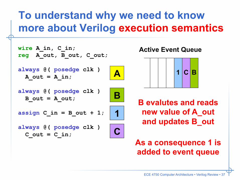
ECE 4750 Computer Architecture • Verilog Review • 37
To understand why we need to know more about Verilog execution semantics
Active Event Queue
A B C
B
1
C
wire A_in, C_in; reg A_out, B_out, C_out; always @( posedge clk ) A_out = A_in; always @( posedge clk ) B_out = A_out; assign C_in = B_out + 1; always @( posedge clk ) C_out = C_in;
B evalutes and reads new value of A_out and updates B_out
1
As a consequence 1 is added to event queue

ECE 4750 Computer Architecture • Verilog Review • 38
To understand why we need to know more about Verilog execution semantics
Active Event Queue
A B C C 1
Event queue is emptied before we go
to next clock cycle
B
1
C
wire A_in, C_in; reg A_out, B_out, C_out; always @( posedge clk ) A_out = A_in; always @( posedge clk ) B_out = A_out; assign C_in = B_out + 1; always @( posedge clk ) C_out = C_in;

ECE 4750 Computer Architecture • Verilog Review • 39
To understand why we need to know more about Verilog execution semantics
A
A
+1
B C
+1
B
1
C
wire A_in, C_in; reg A_out, B_out, C_out; always @( posedge clk ) A_out = A_in; always @( posedge clk ) B_out = A_out; assign C_in = B_out + 1; always @( posedge clk ) C_out = C_in;

ECE 4750 Computer Architecture • Verilog Review • 40
Non-blocking procedural assignments add an extra event queue
A
B
1
C
wire A_in, C_in; reg A_out, B_out, C_out; always @( posedge clk ) A_out <= A_in; always @( posedge clk ) B_out <= A_out; assign C_in = B_out + 1; always @( posedge clk ) C_out <= C_in;
Put evaluation of RHS of non-blocking assignments in AEQ and actual update into NBQ
AEQ: Active Event Queue
NBQ: Non-Blocking Queue
A E
B E
C E
A U
B U
C U

ECE 4750 Computer Architecture • Verilog Review • 41
Non-blocking procedural assignments add an extra event queue
AEQ: Active Event Queue
A
NBQ: Non-Blocking Queue
A U
B U
C U
A U
B U
C U
B
1
C
wire A_in, C_in; reg A_out, B_out, C_out; always @( posedge clk ) A_out <= A_in; always @( posedge clk ) B_out <= A_out; assign C_in = B_out + 1; always @( posedge clk ) C_out <= C_in;
Once RHS of non-blocking assignments have been evaluated and saved results internally, move updated
events from NBQ into AEQ
ECE 4750 Computer Architecture • Verilog Review • 42
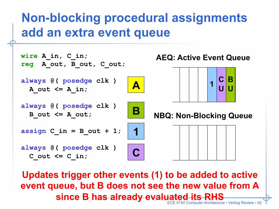
Non-blocking procedural assignments add an extra event queue
AEQ: Active Event Queue
A
NBQ: Non-Blocking Queue
B U
C U 1
B
1
C
wire A_in, C_in; reg A_out, B_out, C_out; always @( posedge clk ) A_out <= A_in; always @( posedge clk ) B_out <= A_out; assign C_in = B_out + 1; always @( posedge clk ) C_out <= C_in;
Updates trigger other events (1) to be added to active event queue, but B does not see the new value from A
since B has already evaluated its RHS

ECE 4750 Computer Architecture • Verilog Review • 43
Non-blocking procedural assignments add an extra event queue wire A_in, C_in; reg A_out, B_out, C_out; always @( posedge clk ) A_out <= A_in; always @( posedge clk ) B_out <= A_out; assign C_in = B_out + 1; always @( posedge clk ) C_out <= C_in;
A
+1
B C

ECE 4750 Computer Architecture • Verilog Review • 44
Non-blocking procedural assignments add an extra event queue
wire A_in, C_in; reg A_out, B_out, C_out; always @( posedge clk ) begin A_out <= A_in; B_out <= A_out; C_out <= C_in; end assign C_in = B_out + 1;
wire A_in, C_in; reg A_out, B_out, C_out; always @( posedge clk ) begin C_out <= C_in; B_out <= A_out; A_out <= A_in; end assign C_in = B_out + 1;
The order of non-blocking assignments does not matter!

ECE 4750 Computer Architecture • Verilog Review • 45
Common patterns for latch and flip-flop inference
always @(*) begin if ( clk ) Q <= D; end
always @( posedge clk ) begin Q <= D; end
always @( posedge clk ) begin if ( enable ) Q <= D; end
D Q X next_X clk
D Q X next_X clk
D Q X next_X clk
enable

ECE 4750 Computer Architecture • Verilog Review • 46
Five guidelines for using combinational and sequential always blocks
1. Clearly distinguish always blocks meant for combinational logic from those meant for sequential logic, do not mix combinational logic and sequential logic in the same always block
2. Only use blocking assignments (=) in combinational always blocks
3. Only use non-blocking assignments (<=) in sequential always blocks
4. Try to put as little logic in a sequential always block as possible
5. Do not assign to the same variable from more than one always block

ECE 4750 Computer Architecture • Verilog Review • 47
Functional Verilog is used to model the abstract function of a hardware module
• Characterized by heavy use of sequential blocking statements in large always blocks
• Many constructs are not synthesizable but can be useful for behavioral modeling – Data dependent for and while loops – Additional behavioral datatypes : integer, real – Magic initialization blocks : initial – Magic delay statements: #<delay>

ECE 4750 Computer Architecture • Verilog Review • 48
Verilog can be used to model the high-level function of a hardware block module factorial( input [ 7:0] in, output reg [15:0] out ); integer num_calls; initial num_calls = 0; integer multiplier; integer result; always @(*) begin multiplier = in; result = 1; while ( multiplier > 0 ) begin result = result * multiplier; multiplier = multiplier - 1; end out = result; num_calls = num_calls + 1; end endmodule
Data dependent while loop
Variables of type integer
Initial statement

ECE 4750 Computer Architecture • Verilog Review • 49
Delay statements should only be used in test harnesses
module mux4 ( input a, input b, input c, input d, input [1:0] sel, output out ); wire #10 t0 = ~( (sel[1] & c) | (~sel[1] & a) ); wire #10 t1 = ~( (sel[1] & d) | (~sel[1] & b) ); wire #10 out = ~( (t0 | sel[0]) & (t1 | ~sel[0]) ); endmodule
Although this will add a delay for simulation, these are ignored in
synthesis

ECE 4750 Computer Architecture • Verilog Review • 50
Even synthesizable blocks can be more functional in nature module ALU ( input [31:0] in0, input [31:0] in1, input [ 1:0] fn, output [31:0] out ); assign out = ( fn == 2'd0 ) ? ( in0 + in1 ) : ( fn == 2'd1 ) ? ( in0 - in1 ) : ( fn == 2'd9 ) ? ( in1 >> in0 ) : ( fn == 2'd10 ) ? ( in1 >>> in0 ) : 32'bx; endmodule
Although this module is synthesizable, it is unlikely to produce the desired hardware.
+
–
>>
>>>

ECE 4750 Computer Architecture • Verilog Review • 51
System tasks are used for test harnesses and simulation management reg [ 1023:0 ] exe_filename; initial begin // This turns on VCD (plus) output $vcdpluson(0); // This gets the program to load into memory from the command line if ( $value$plusargs( "exe=%s", exe_filename ) ) $readmemh( exe_filename, mem.m ); else begin $display( "ERROR: No executable specified! (use +exe=<filename>)" ); $finish; end // Stobe reset #0 reset = 1; #38 reset = 0; end

ECE 4750 Computer Architecture • Verilog Review • 52
Which abstraction is the right one?
Designers usually use a mix of all three! Early on in the design process they might use mostly behavioral models. As the design is refined, the behavioral models begin to be replaced by dataflow models. Finally, the designers use automatic tools to synthesize a low-level gate-level model.
High-Level Behavioral
Register Transfer Level
Gate Level

ECE 4750 Computer Architecture • Verilog Review • 53
FA FA FA FA
module adder( input [3:0] A, B, output cout, output [3:0] S );
wire c0, c1, c2; FA fa0( A[0], B[0], 1�b0, c0, S[0] ); FA fa1( A[1], B[1], c0, c1, S[1] ); FA fa2( A[2], B[2], c1, c2, S[2] ); FA fa3( A[3], B[3], c2, cout, S[3] );
endmodule
Verilog Review • Data types • Structural Verilog • Behavioral Verilog
– Gate level – Register transfer level – Functional level
• Parameterized Static Elaboration
• Greatest Common Divisor

ECE 4750 Computer Architecture • Verilog Review • 54
Static elaboration enables generation of hardware at synthesis time
Register Transfer Level
Gate Level
Auto Place + Route
Test Results
Simulate
Elaborated Design
Logic Synthesis
Static Elaboration
Test Results
Simulate
We will look at two forms of static elaboration: (1) parameters and
(2) generate blocks

ECE 4750 Computer Architecture • Verilog Review • 55
Parameters are bound during static elaboration creating flexible modules module vcMux2 #( parameter WIDTH = 1 ) ( input [WIDTH-1:0] in0, in1, input [1:0] sel, output reg [WIDTH-1:0] out ); always @(*) begin case ( sel ) 1�d0 : out = in0; 1�d1 : out = in1; default : out = {WIDTH{1�bx}}; endcase end endmodule
Instantiation Syntax vcMux2#(32) alu_mux ( .in0 (op1), .in1 (bypass), .sel (alu_mux_sel), .out (alu_mux_out) );

ECE 4750 Computer Architecture • Verilog Review • 56
Parameters are bound during static elaboration creating flexible modules module vcERDFF_pf #( parameter WIDTH = 1, parameter RESET_VALUE = 0 ) ( input clk, input reset, input [WIDTH-1:0] d, input en, output reg [WIDTH-1:0] q ); always @( posedge clk ) if ( reset ) q <= RESET_VALUE; else if ( en ) q <= d; endmodule
Instantiation Syntax vcERDFF_pf#(32,32�h10) pc_pf ( .clk (clk), .reset (reset), .en (pc_enable), .d (pc_mux_out), .q (pc) );

ECE 4750 Computer Architecture • Verilog Review • 57
Generate blocks can execute loops and conditionals during static elaboration module adder ( input [3:0] op1,op2, output cout, output [3:0] sum ); wire [4:0] carry; assign carry[0] = 1�b0; assign cout = carry[4] genvar i; generate for ( i = 0; i < 4; i = i+1 ) begin : ripple FA fa( op1[i], op2[i], carry[i], carry[i+1] ); end endgenerate endmodule
All genvars must be disappear after static elaboration
Generated names will have ripple[i]. prefix

ECE 4750 Computer Architecture • Verilog Review • 58
Combining parameters + generate blocks enables more powerful elaboration module adder#( parameter WIDTH = 1 ) ( input [WIDTH-1:0] op1,op2, output cout, output [WIDTH-1:0] sum );
wire [WIDTH:0] carry; assign carry[0] = 1�b0; assign cout = carry[WIDTH];
genvar i; generate for ( i = 0; i < WIDTH; i = i+1 ) begin : ripple FA fa( op1[i], op2[i], carry[i], carry[i+1] ); end endgenerate
endmodule
Use parameter for loop bounds

ECE 4750 Computer Architecture • Verilog Review • 59
Generate statements are useful for more than just module instantiation module adder#( parameter WIDTH = 1 ) ( input [WIDTH-1:0] op1,op2, output cout, output [WIDTH-1:0] sum );
wire [WIDTH:0] carry; assign carry[0] = 1�b0; assign cout = carry[WIDTH];
genvar i; generate for ( i = 0; i < WIDTH; i = i+1 ) begin : ripple assign {carry[i+1],sum[i]} = op1[i] + op2[i] + carry[i]; end endgenerate
endmodule
Statically elaborating many continuous
assignments

ECE 4750 Computer Architecture • Verilog Review • 60
Traditionally designers have resorted to behavioral inference for elaboration module adder#( parameter WIDTH = 1 ) ( input [WIDTH-1:0] op1,op2, output cout, output reg [WIDTH-1:0] sum );
reg [WIDTH:0] carry; assign cout = carry[WIDTH];
integer i; always @(*) begin assign carry[0] = 1�b0; for ( i = 0; i < WIDTH; i = i+1 ) {carry[i+1],sum[i]} = op1[i] + op2[i] + carry[i]; end end
endmodule
Although similar to generate block, this
code has very different semantics!

ECE 4750 Computer Architecture • Verilog Review • 61
FA FA FA FA
module adder( input [3:0] A, B, output cout, output [3:0] S );
wire c0, c1, c2; FA fa0( A[0], B[0], 1�b0, c0, S[0] ); FA fa1( A[1], B[1], c0, c1, S[1] ); FA fa2( A[2], B[2], c1, c2, S[2] ); FA fa3( A[3], B[3], c2, cout, S[3] );
endmodule
Verilog Review • Data types • Structural Verilog • Behavioral Verilog
– Gate level – Register transfer level – Functional level
• Parameterized Static Elaboration
• Greatest Common Divisor

ECE 4750 Computer Architecture • Verilog Review • 62
Functional GCD model is written within a single always block with C like structure module gcdGCDUnit_behav#( parameter W = 16 ) ( input [W-1:0] inA, inB, output [W-1:0] out );
reg [W-1:0] A, B, out, swap; integer done;
always @(*) begin done = 0; A = inA; B = inB;
while ( !done ) begin if ( A < B ) swap = A; A = B; B = swap; else if ( B != 0 ) A = A - B; else done = 1; end
out = A; end
endmodule
Test harness will simply set the input operands and check the output.
ECE 4750 Computer Architecture • Verilog Review • 63
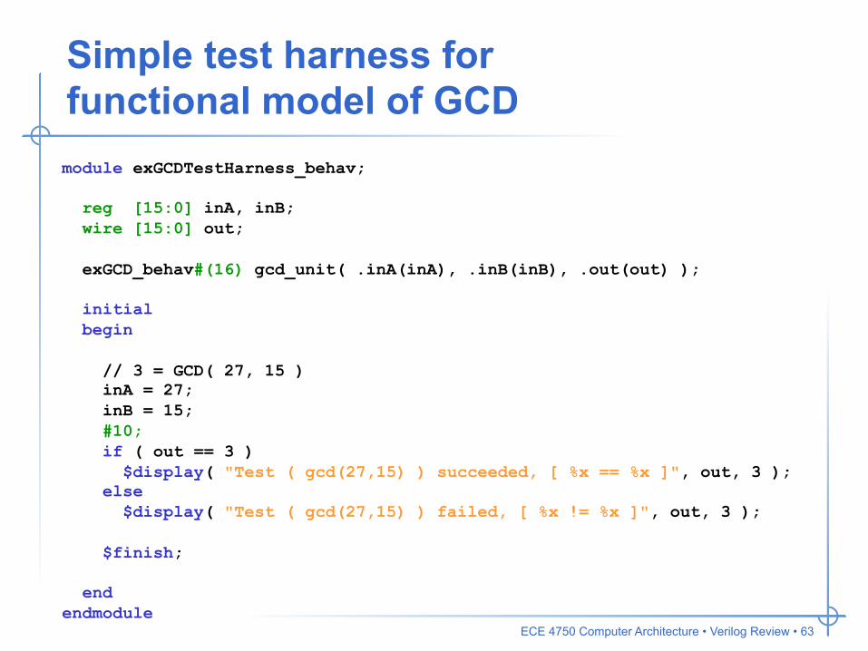
Simple test harness for functional model of GCD module exGCDTestHarness_behav; reg [15:0] inA, inB; wire [15:0] out; exGCD_behav#(16) gcd_unit( .inA(inA), .inB(inB), .out(out) ); initial begin // 3 = GCD( 27, 15 ) inA = 27; inB = 15; #10; if ( out == 3 ) $display( "Test ( gcd(27,15) ) succeeded, [ %x == %x ]", out, 3 ); else $display( "Test ( gcd(27,15) ) failed, [ %x != %x ]", out, 3 ); $finish; end endmodule

ECE 4750 Computer Architecture • Verilog Review • 64
Behavioral GCD model is written within a single always block with C like structure module gcdGCDUnit_behav#( parameter W = 16 ) ( input [W-1:0] inA, inB, output [W-1:0] Y );
reg [W-1:0] A, B, Y, swap; integer done;
always @(*) begin done = 0; A = inA; B = inB;
while ( !done ) begin if ( A < B ) swap = A; A = B; B = swap; else if ( B != 0 ) A = A - B; else done = 1; end
Y = A; end
endmodule
Our goal now is to design an RTL hardware block which implements this high-level behavior. What does
the RTL implementation need?
State
Less-Than Comparator
Equal Comparator
Subtractor

ECE 4750 Computer Architecture • Verilog Review • 65
The first step is to carefully design an appropriate port interface
operands_rdy
operands_val
operands_bits_A
operands_bits_B
result_bits_data
result_rdy
result_val
clk reset

ECE 4750 Computer Architecture • Verilog Review • 66
Next develop a datapath which has the proper functional units
B
A = inA; B = inB;
while ( !done ) begin if ( A < B ) swap = A; A = B; B = swap; else if ( B != 0 ) A = A - B; else done = 1; end
Y = A;
zero? lt
A

ECE 4750 Computer Architecture • Verilog Review • 67
Next develop a datapath which has the proper functional units
B
A = inA; B = inB;
while ( !done ) begin if ( A < B ) swap = A; A = B; B = swap; else if ( B != 0 ) A = A - B; else done = 1; end
Y = A;
zero? lt
A

ECE 4750 Computer Architecture • Verilog Review • 68
Next develop a datapath which has the proper functional units
B
A = inA; B = inB;
while ( !done ) begin if ( A < B ) swap = A; A = B; B = swap; else if ( B != 0 ) A = A - B; else done = 1; end
Y = A;
zero? lt
A sub

ECE 4750 Computer Architecture • Verilog Review • 69
Finally add the control unit to sequence the datapath
B
A mux sel
A reg en
B mux sel
B reg en A < B B = 0
A = inA; B = inB;
while ( !done ) begin if ( A < B ) swap = A; A = B; B = swap; else if ( B != 0 ) A = A - B; else done = 1; end
Y = A;
zero? lt
A sub

ECE 4750 Computer Architecture • Verilog Review • 70
Datapath module interface module gcdGCDUnitDpath_sstr#( parameter W = 16 ) ( input clk, // Data signals input [W-1:0] operands_bits_A, input [W-1:0] operands_bits_B, output [W-1:0] result_bits_data, // Control signals (ctrl->dpath) input A_en, input B_en, input [1:0] A_mux_sel, input B_mux_sel, // Control signals (dpath->ctrl) output B_zero, output A_lt_B );
B
A sel
A en
B sel
B en A < B B = 0
zero? lt A
sub
ECE 4750 Computer Architecture • Verilog Review • 71
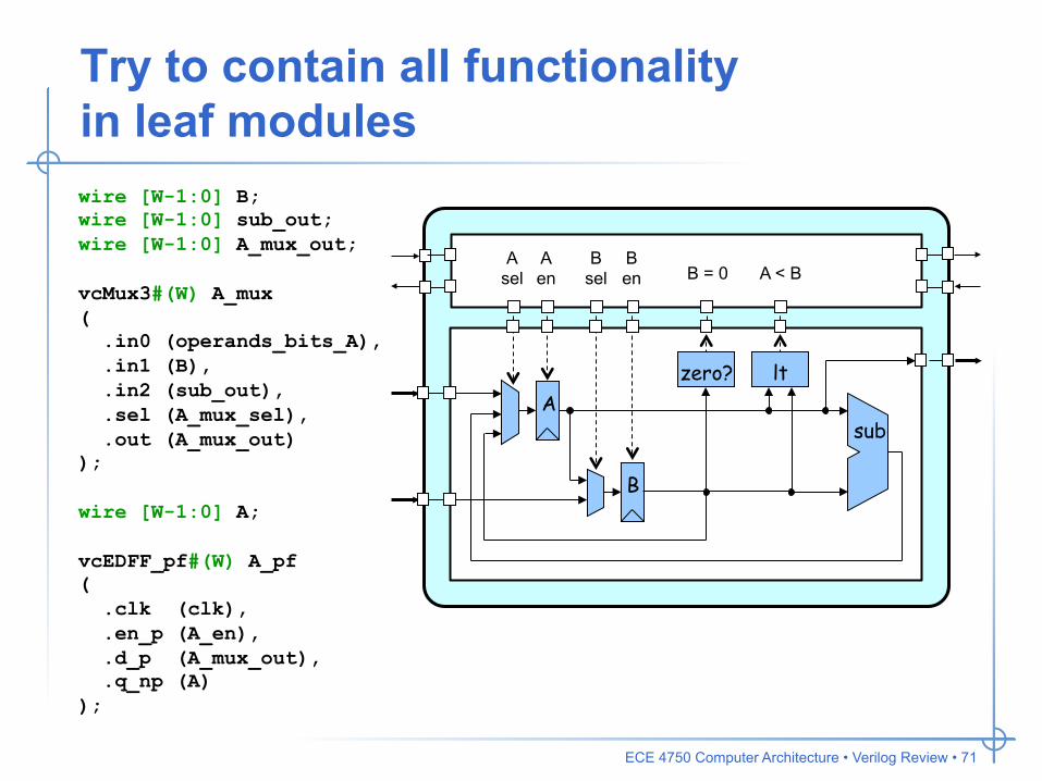
Try to contain all functionality in leaf modules wire [W-1:0] B; wire [W-1:0] sub_out; wire [W-1:0] A_mux_out; vcMux3#(W) A_mux ( .in0 (operands_bits_A), .in1 (B), .in2 (sub_out), .sel (A_mux_sel), .out (A_mux_out) ); wire [W-1:0] A; vcEDFF_pf#(W) A_pf ( .clk (clk), .en_p (A_en), .d_p (A_mux_out), .q_np (A) );
B
A sel
A en
B sel
B en A < B B = 0
zero? lt A
sub

ECE 4750 Computer Architecture • Verilog Review • 72
Try to contain all functionality in leaf modules wire [W-1:0] B; wire [W-1:0] sub_out; wire [W-1:0] A_mux_out; vcMux3#(W) A_mux ( .in0 (operands_bits_A), .in1 (B), .in2 (sub_out), .sel (A_mux_sel), .out (A_mux_out) ); wire [W-1:0] A; vcEDFF_pf#(W) A_pf ( .clk (clk), .en_p (A_en), .d_p (A_mux_out), .q_np (A) );
wire [W-1:0] B_mux_out; vcMux2#(W) B_mux ( .in0 (operands_bits_B), .in1 (A), .sel (B_mux_sel), .out (B_mux_out) ); vcEDFF_pf#(W) B_pf ( .clk (clk), .en_p (B_en), .d_p (B_mux_out), .q_np (B) ); assign B_zero = ( B == 0 ); assign A_lt_B = ( A < B ); assign sub_out = A - B; assign result_bits_data = A;
Continuous assignment
combinational logic is fine
Using explicit state helps eliminate
issues with non-blocking
assignments

ECE 4750 Computer Architecture • Verilog Review • 73
Control unit requires a simple state machine for valid/ready signals
WAIT
CALC
DONE
operands_val
!( A < B ) & ( B = 0 )
result_rdy
Waiting for new input operands
Swapping and subtracting
Waiting for consumer to take the result
reset

ECE 4750 Computer Architecture • Verilog Review • 74
Implementing the control logic finite state machine in Verilog
localparam WAIT = 2'd0; localparam CALC = 2'd1; localparam DONE = 2'd2; reg [1:0] state_next; wire [1:0] state; vcRDFF_pf#(2,WAIT) state_pf ( .clk (clk), .reset_p (reset), .d_p (state_next), .q_np (state) ); Explicit state in the control
logic is also a good idea!
Localparams are not really parameters at all. They are
scoped constants.

ECE 4750 Computer Architecture • Verilog Review • 75
Implementing the control signal outputs for the finite state machine reg [6:0] cs; always @(*) begin // Default control signals A_mux_sel = A_MUX_SEL_X; A_en = 1'b0; B_mux_sel = B_MUX_SEL_X; B_en = 1'b0; operands_rdy = 1'b0; result_val = 1'b0; case ( state ) WAIT : ... CALC : ... DONE : ... endcase end
WAIT : begin A_mux_sel = A_MUX_SEL_IN; A_en = 1'b1; B_mux_sel = B_MUX_SEL_IN; B_en = 1'b1; operands_rdy = 1'b1; end CALC : if ( A_lt_B ) A_mux_sel = A_MUX_SEL_B; A_en = 1'b1; B_mux_sel = B_MUX_SEL_A; B_en = 1'b1; else if ( !B_zero ) A_mux_sel = A_MUX_SEL_SUB; A_en = 1'b1; end DONE : result_val = 1'b1;

ECE 4750 Computer Architecture • Verilog Review • 76
Implementing the state transitions for the finite state machine always @(*) begin // Default is to stay in the same state state_next = state; case ( state ) WAIT : if ( operands_val ) state_next = CALC; CALC : if ( !A_lt_B && B_zero ) state_next = DONE; DONE : if ( result_rdy ) state_next = WAIT; endcase end
WAIT
CALC
DONE
operands_val
!( A < B ) & ( B = 0 )
result_rdy
reset

ECE 4750 Computer Architecture • Verilog Review • 77
RTL test harness requires properly handling the ready/valid signals
B
A sel
A en
B sel
B en A < B B = 0
zero? lt A
sub
Generic Test Source
Generic Test Sink

ECE 4750 Computer Architecture • Verilog Review • 78
We can compare the functional and RTL implementations to verify correctness
Test Inputs
Functional Model
RTL Model
Test Outputs Test Outputs
Identical?

ECE 4750 Computer Architecture • Verilog Review • 79
Take away points • Structural Verilog for describing a hw schematic textually • Verilog can model hardware at three levels of abstraction:
gate level, register transfer level, and behavioral • Understanding the Verilog execution semantics is critical
for understanding blocking + non-blocking assignments • Designers must have the hardware they are trying to
create in mind when they write their Verilog • Parameterized models provide the foundation for
reusable libraries of components • Begin your RTL design by identifying the external
interface and then move on to partition your design into datapaths and control logic