verilog tutorial speaker : t.a. chung-yuan lin. traditional approach gate level design schematic...
TRANSCRIPT

Verilog Tutorial
Speaker : T.A. Chung-Yuan Lin

Traditional approach
Gate level design Schematic design
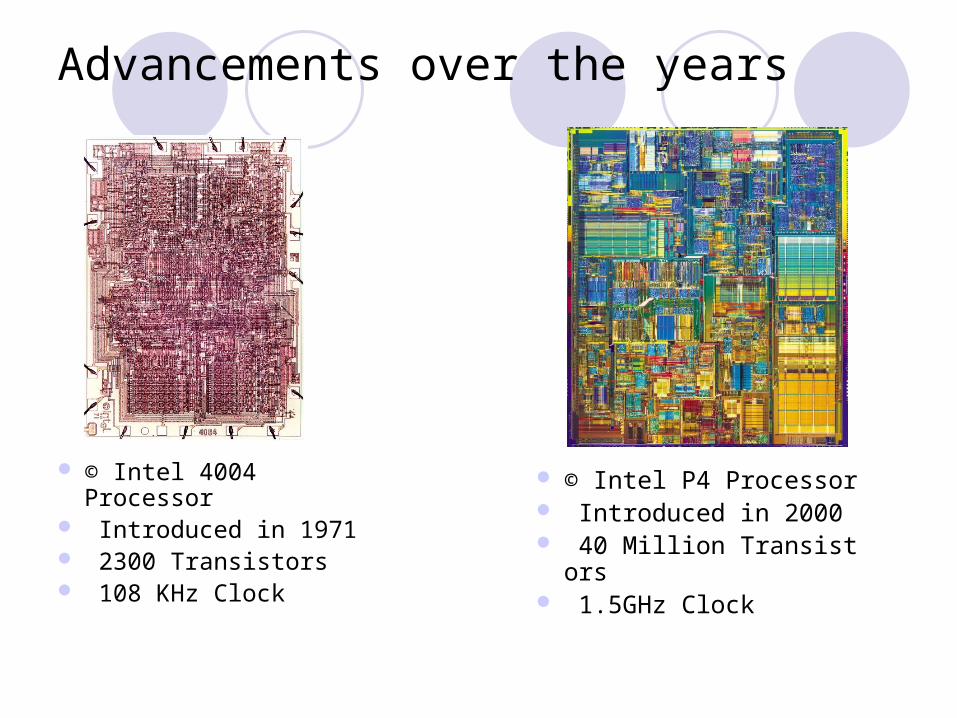
Advancements over the years
© Intel 4004 Processor
Introduced in 1971 2300 Transistors 108 KHz Clock
© Intel P4 Processor Introduced in 2000 40 Million Transistors 1.5GHz Clock
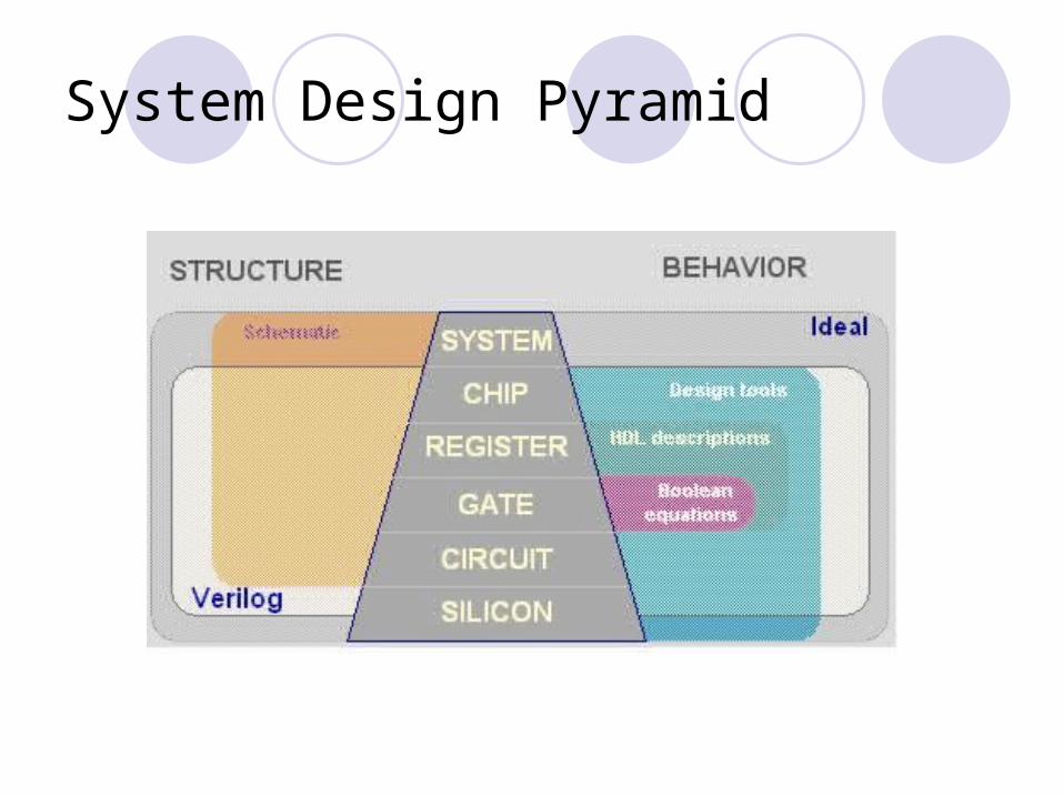
System Design Pyramid
History:
Need: a simple, intuitive and effective way of describing digital circuits for modeling, simulation and analysis.
Developed in 1984-85 by Philip MoorbyIn 1990 Cadence opened the language to t
he publicStandardization of language by IEEE in 19
95

Top-Down Design Approach

Definition of Module
Interface: port and parameter declaration
Body: Internal part of module
Add-ons (optional)
Some points to remember
The name of Module
Comments in Verilog One line comment (// ………….) Block Comment (/*…………….*/)
Description of Module (optional but suggested)
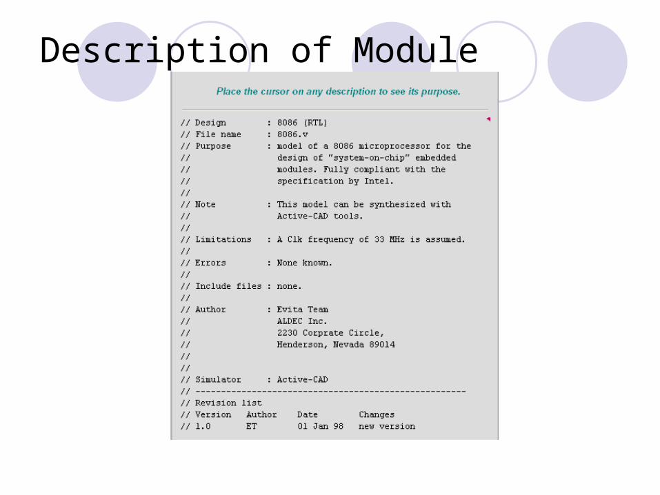
Description of Module
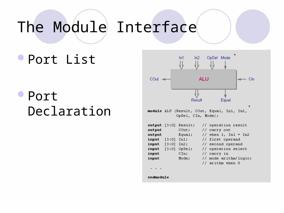
The Module Interface
Port List
Port Declaration

Specifications of Ports
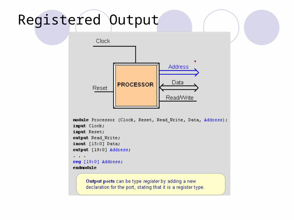
Registered Output
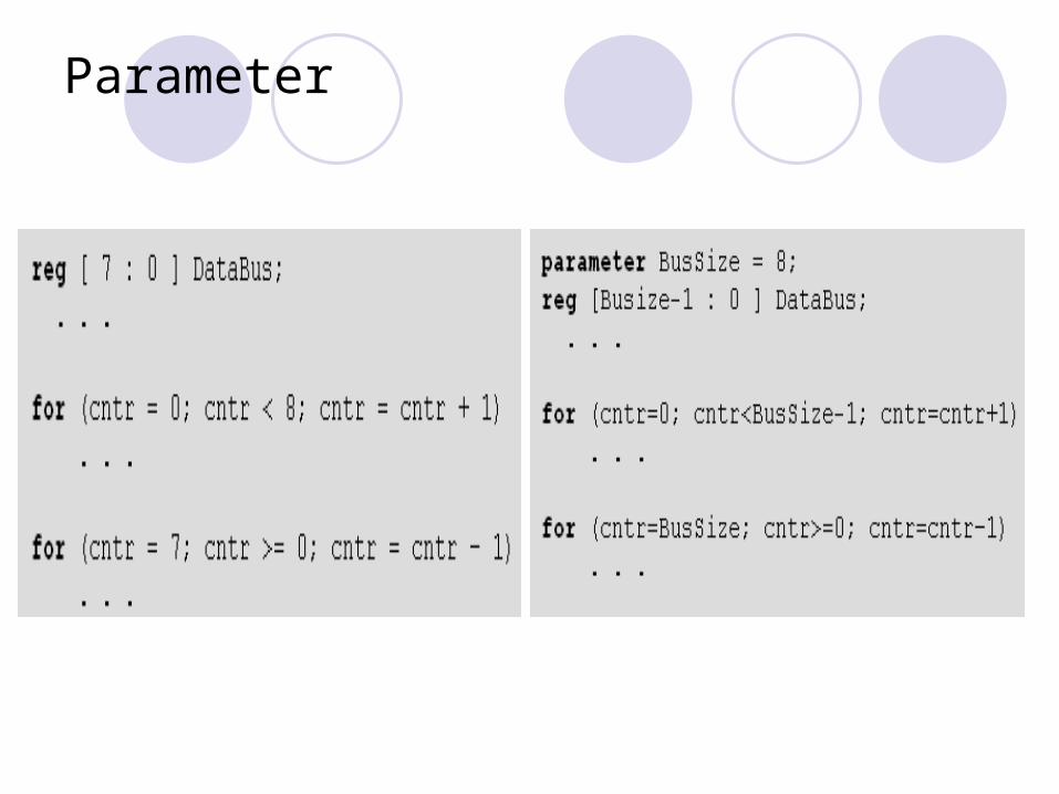
Parameter
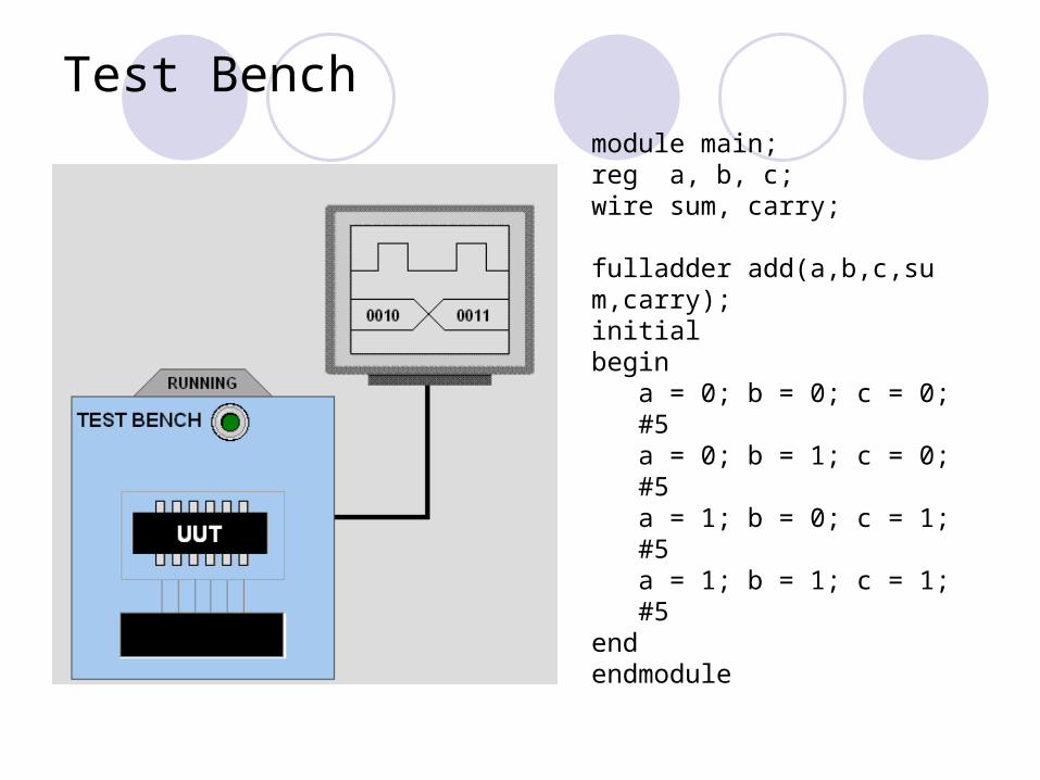
Test Benchmodule main;reg a, b, c; wire sum, carry;
fulladder add(a,b,c,sum,carry);initialbegin a = 0; b = 0; c = 0; #5 a = 0; b = 1; c = 0; #5 a = 1; b = 0; c = 1; #5 a = 1; b = 1; c = 1; #5endendmodule
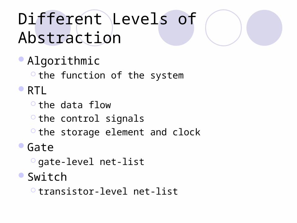
Different Levels of Abstraction
Algorithmic the function of the system
RTL the data flow the control signals the storage element and clock
Gate gate-level net-list
Switch transistor-level net-list

Verilog for Digital System Design
Structural description net-list using primitive gates and switches continuous assignment using Verilog operators
RTL functional description timing controls and concurrency specification procedural blocks (always and initial) registers and latches
C + timing controls + concurrencyAn HDL to specify your design
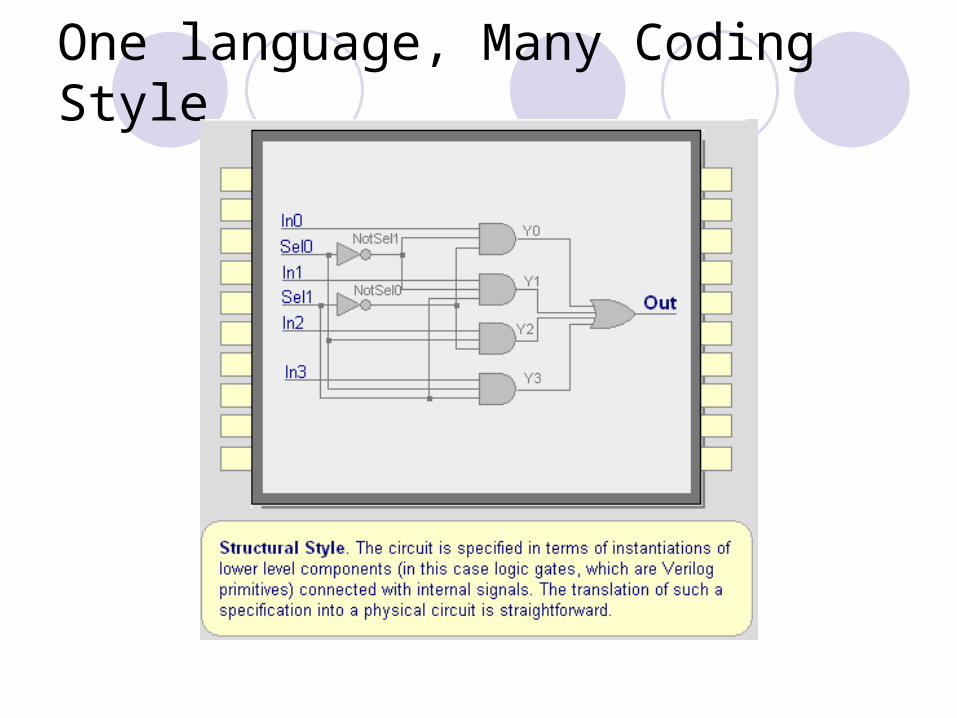
One language, Many Coding Style
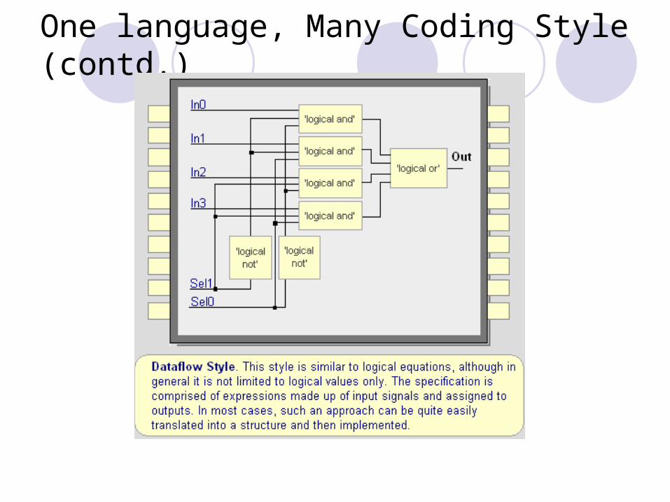
One language, Many Coding Style (contd.)

One language, Many Coding Style (contd.)

Structural style: Verilog Code
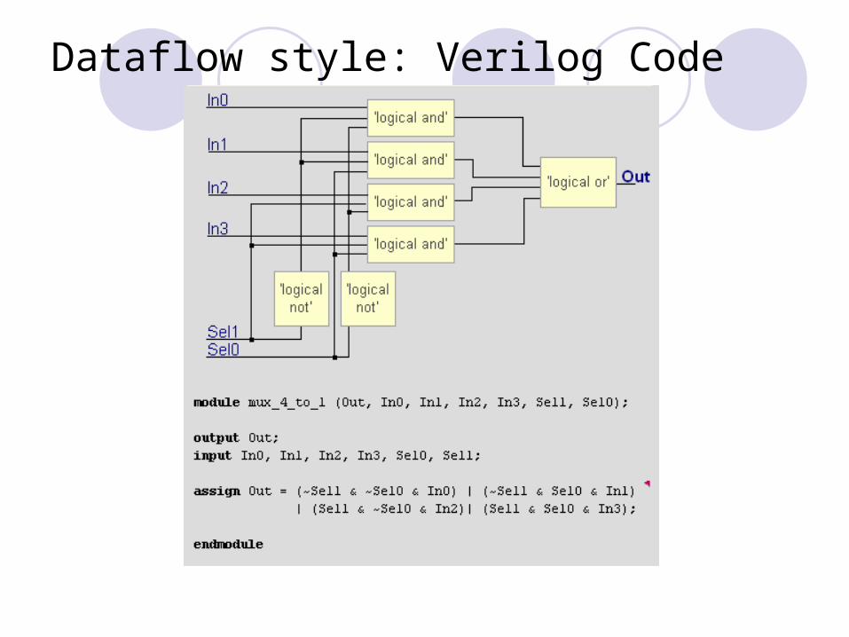
Dataflow style: Verilog Code

Behavioral style: Verilog Code
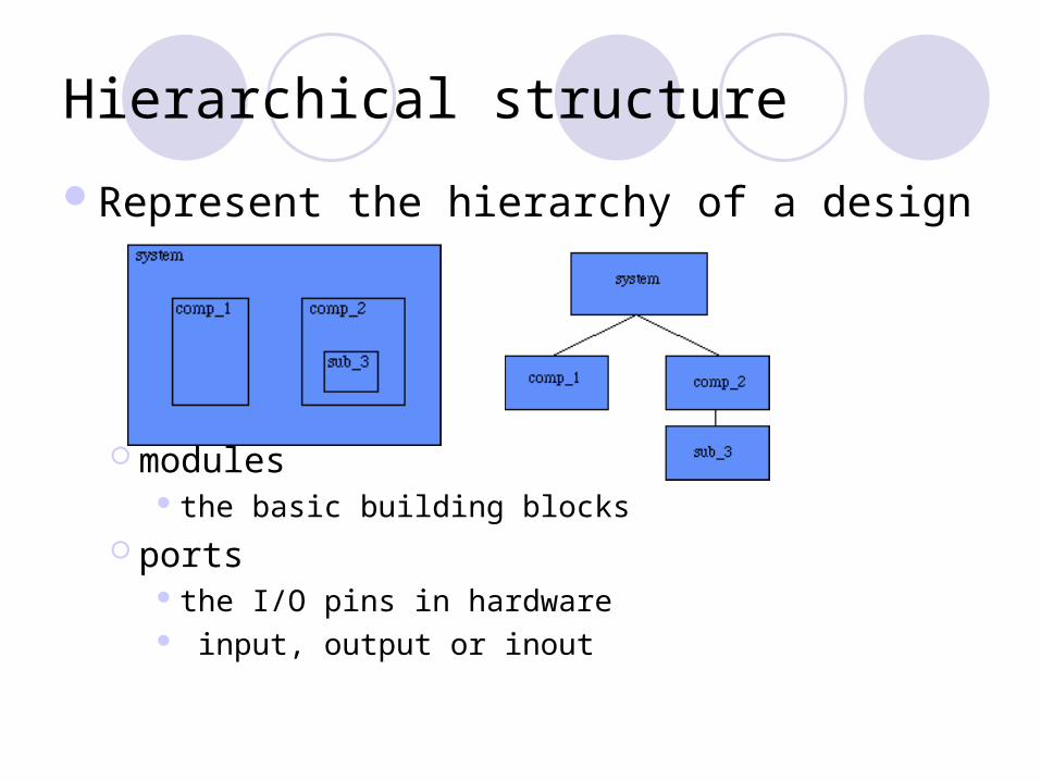
Hierarchical structure
Represent the hierarchy of a design
modules the basic building blocks
ports the I/O pins in hardware input, output or inout

Examples
4-bit addermodule add4 (s,c3,ci,a,b)
input [3:0] a,b ; // port declarations
input ci ;
output [3:0] s : // vector
output c3 ;
wire [2:0] co ;add a0 (co[0], s[0], a[0], b[0], ci) ;
add a1 (co[1], s[1], a[1], b[1], co[0]) ;
add a2 (co[2], s[2], a[2], b[2], co[1]) ;
add a3 (c3, s[3], a[3], b[3], co[2]) ;
endmodule a0a1a2a3c3 ci
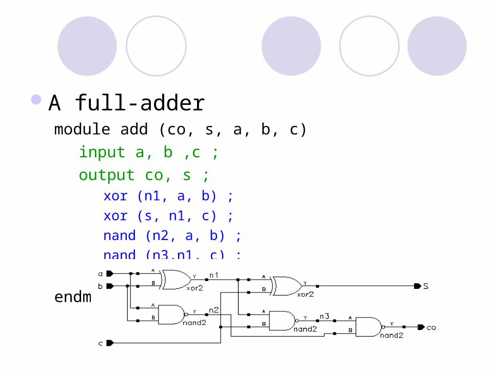
A full-addermodule add (co, s, a, b, c)
input a, b ,c ;
output co, s ;xor (n1, a, b) ;
xor (s, n1, c) ;
nand (n2, a, b) ;
nand (n3,n1, c) ;
nand (co, n3,n2) ;
endmodule
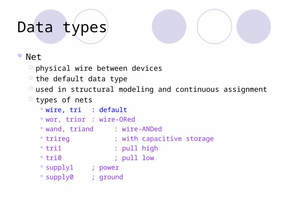
Data types
Net physical wire between devices the default data type used in structural modeling and continuous assignment types of nets
wire, tri : default wor, trior : wire-ORed wand, triand : wire-ANDed trireg : with capacitive storage tri1 : pull high tri0 ; pull low supply1 ; power supply0 ; ground
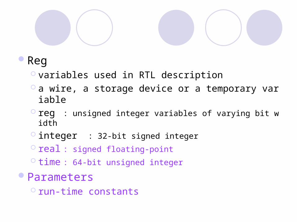
Reg variables used in RTL description a wire, a storage device or a temporary variable reg : unsigned integer variables of varying bit width integer : 32-bit signed integer real : signed floating-point time : 64-bit unsigned integer
Parameters run-time constants
Modeling Structures
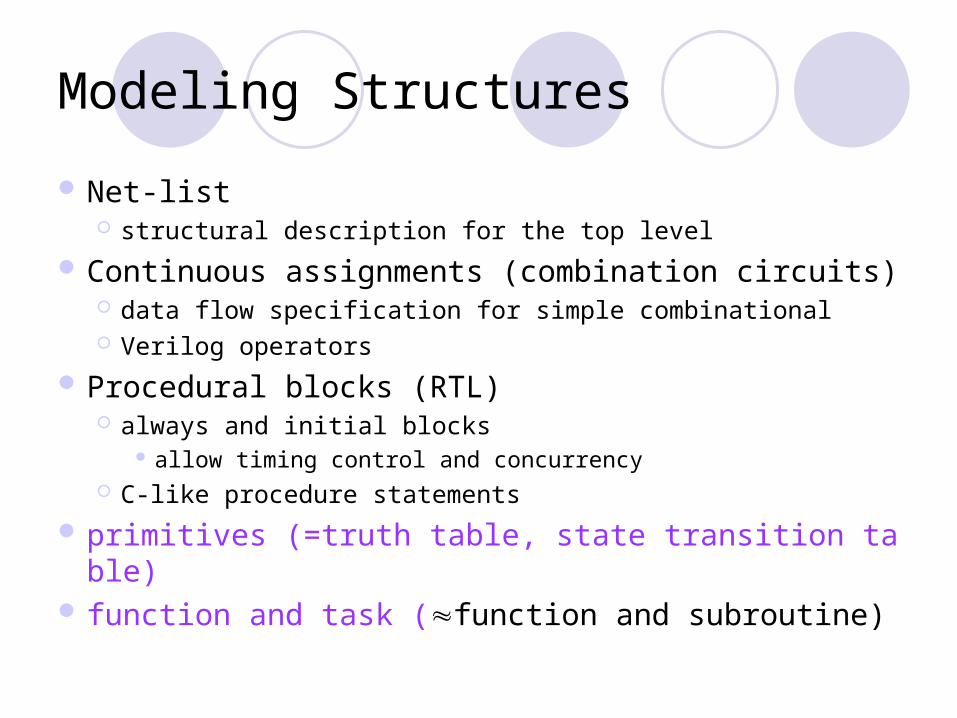
Net-list structural description for the top level
Continuous assignments (combination circuits) data flow specification for simple combinational Verilog operators
Procedural blocks (RTL) always and initial blocks
allow timing control and concurrency C-like procedure statements
primitives (=truth table, state transition table) function and task (function and subroutine)

Gate-Level Modeling
Net-list description built-in primitives gates
A full-addermodule add (co, s, a, b, c)
input a, b ,c ;
output co, s ;xor (n1, a, b) ;
xor (s, n1, c) ;
nand (n2, a, b) ;
nand (n3,n1, c) ;
nand (co, n3,n2) ;
endmodule

Verilog Primitives
Basic logic gates only and or not buf xor nand nor xnor bufif1, bufif0 notif1, notif0
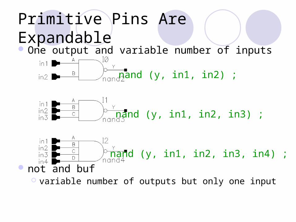
Primitive Pins Are Expandable One output and variable number of inputs
not and buf variable number of outputs but only one input
nand (y, in1, in2) ;
nand (y, in1, in2, in3) ;
nand (y, in1, in2, in3, in4) ;

Continuous Assignments
Describe combinational logicOperands + operatorsDrive values to a net
assign out = a&b ; // and gate assign eq = (a==b) ; // comparator wire #10 inv = ~in ; // inverter with delay wire [7:0] c = a+b ; // 8-bit adder
Avoid logic loops assign a = b + a ; asynchronous design
Operators
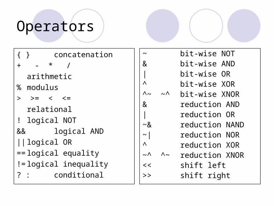
{ } concatenation
+ - * /
arithmetic
% modulus
> >= < <=
relational
! logical NOT
&& logical AND
|| logical OR
== logical equality
!= logical inequality
? : conditional
~ bit-wise NOT& bit-wise AND| bit-wise OR^ bit-wise XOR^~ ~^ bit-wise XNOR& reduction AND| reduction OR~& reduction NAND~| reduction NOR^ reduction XOR~^ ^~ reduction XNOR<< shift left>> shift right

Logical, bit-wise and unary operatorsa = 1011; b = 0010
logical bit-wise unary
a || b = 1 a | b = 1011 |a = 1
a && b = 1 a &b = 0010 &a = 0
Conditional operatorassign z = ({s1,s0} == 2'b00) ? IA :
({s1,s0} == 2'b01) ? IB :
({s1,s0} == 2'b10) ? IC :
({s1,s0} == 2'b11) ? ID :
1'bx ;
assign s = (op == ADD) ? a+b : a-b ;

Operator Precedence
[ ] bit-select or part-select
( ) parentheses
!, ~ logical and bit-wise negation
&, |, ~&, ~|, ^, ~^, ^~reduction operators
+, - unary arithmetic
{ } concatenation
*, /, % arithmetic
+, - arithmetic
<<, >> shift
>, >=, <, <=
relational
==, != logical equality
& bit-wise AND
^, ^~, ~^
bit-wise XOR and XNOR
| bit-wise OR
&&logical AND
|| logical OR
? : conditional

RTL Modeling
Describe the system at a high level of abstraction Specify a set of concurrently active procedural
blocks procedural blocks = digital circuits
Procedural blocks initial blocks
test-fixtures to generate test vectors initial conditions
always blocks can be combinational circuits can imply latches or flip-flops

Procedural blocks have the following components procedural assignment statements timing controls high-level programming language constructs
initial cc statementc …c …c …c …c …
always cc statementc …c …c …c …c …
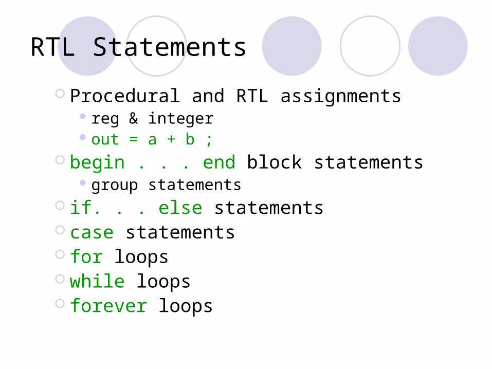
RTL Statements
Procedural and RTL assignments reg & integer out = a + b ;
begin . . . end block statements group statements
if. . . else statements case statements for loops while loops forever loops
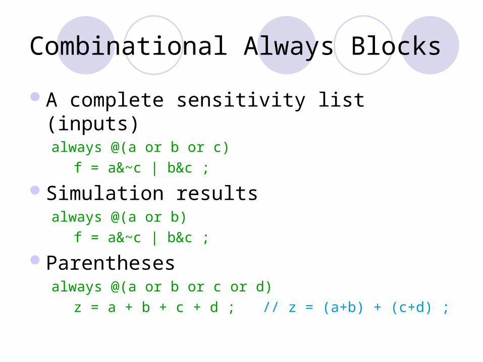
Combinational Always Blocks
A complete sensitivity list (inputs)always @(a or b or c)
f = a&~c | b&c ;
Simulation resultsalways @(a or b)
f = a&~c | b&c ;
Parenthesesalways @(a or b or c or d)
z = a + b + c + d ; // z = (a+b) + (c+d) ;
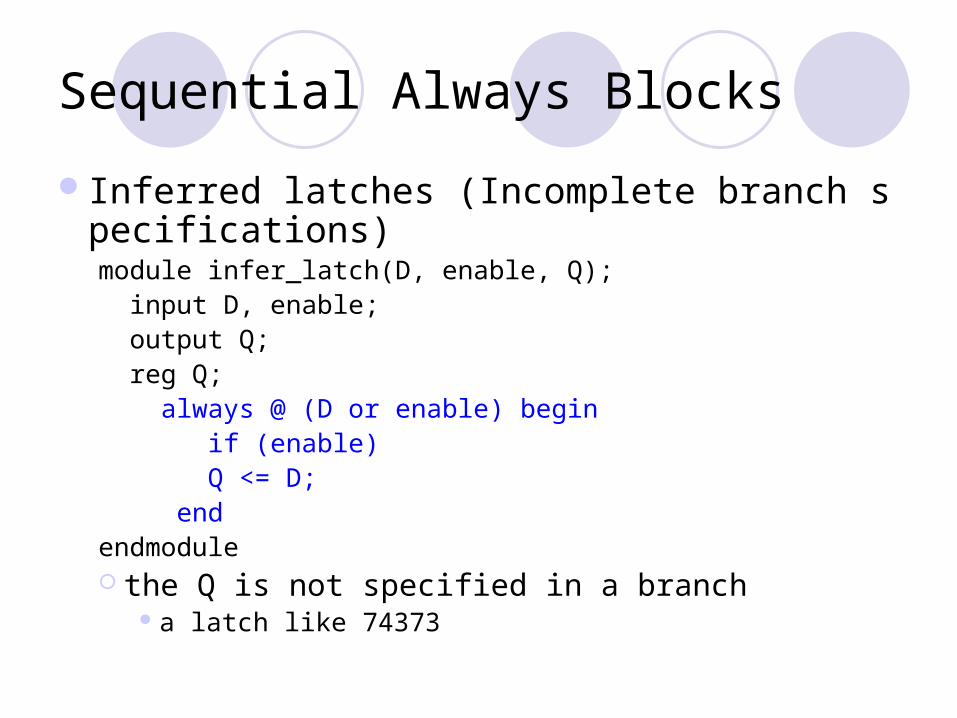
Sequential Always Blocks
Inferred latches (Incomplete branch specifications)module infer_latch(D, enable, Q); input D, enable; output Q; reg Q; always @ (D or enable) begin if (enable) Q <= D; endendmodule the Q is not specified in a branch
a latch like 74373
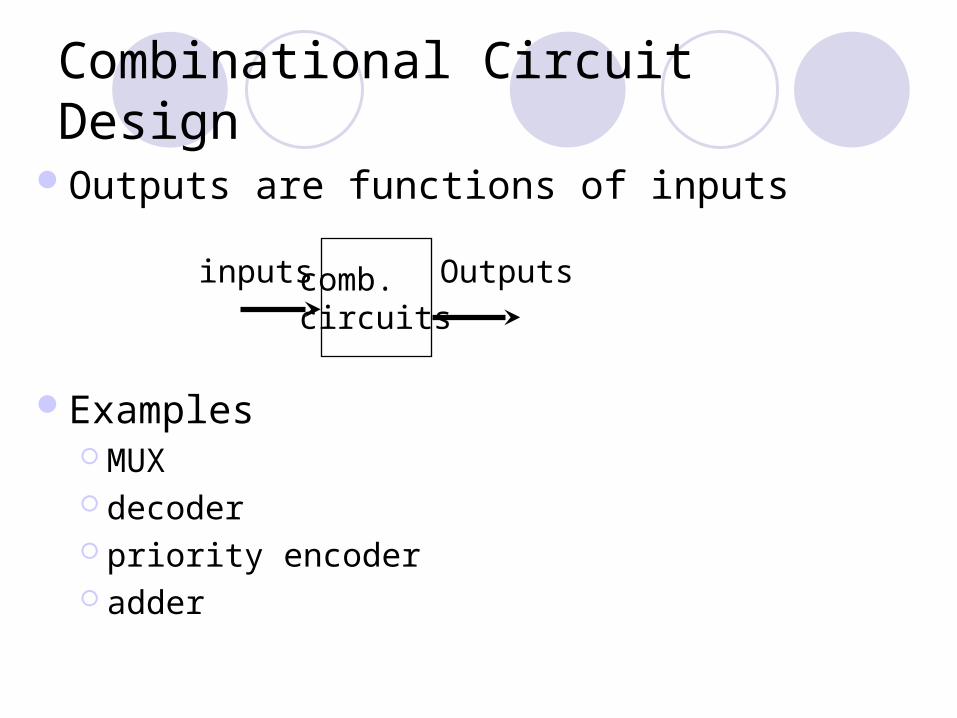
Combinational Circuit Design
Outputs are functions of inputs
Examples MUX decoder priority encoder adder
comb.circuits
inputs Outputs
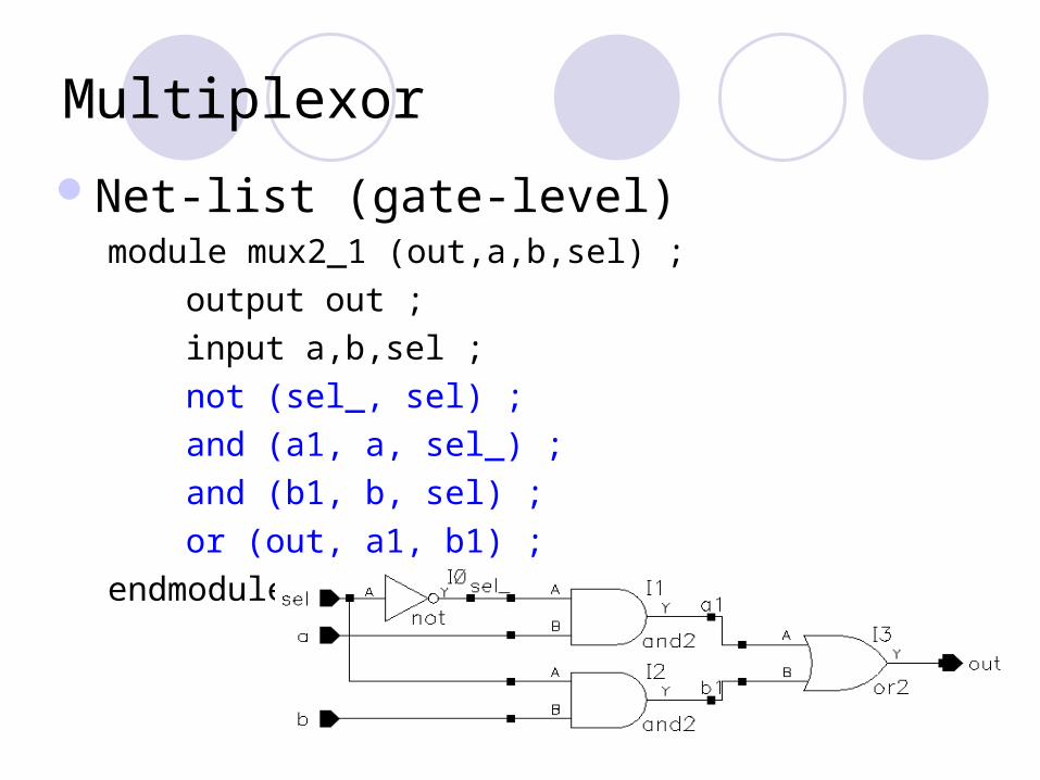
Multiplexor
Net-list (gate-level)module mux2_1 (out,a,b,sel) ;
output out ;
input a,b,sel ;
not (sel_, sel) ;
and (a1, a, sel_) ;
and (b1, b, sel) ;
or (out, a1, b1) ;
endmodule

Multiplexor
Continuous assignmentmodule mux2_1 (out,a,b,sel) ;
output out ;
input a,b,sel ;
assign out = (a&~sel)|(b&sel) ;
endmodule
RTL modelingalways @(a or b or sel)
if(sel)out = b;
elseout = a;

Multiplexor
4-to-1 multiplexormodule mux4_1 (out, in0, in1, in2, in3, sel) ;
output out ;
input in0,in1,in2,in3 ;
input [1:0] sel ;
assign out = (sel == 2'b00) ? in0 :
(sel == 2'b01) ? in1 :
(sel == 2'b10) ? in2 :
(sel == 2'b11) ? in3 :
1'bx ;
endmodule

module mux4_1 (out, in, sel) ; output out ; input [3:0] in ; input [1:0] sel ; reg out ; always @(sel or in) begin
case(sel) 2’d0: out = in[0] ; 2’d1: out = in[1] ; 2’d2: out = in[2] ; 2’d3: out = in[3] ; default: 1’bx ; endcaseend
endmodule
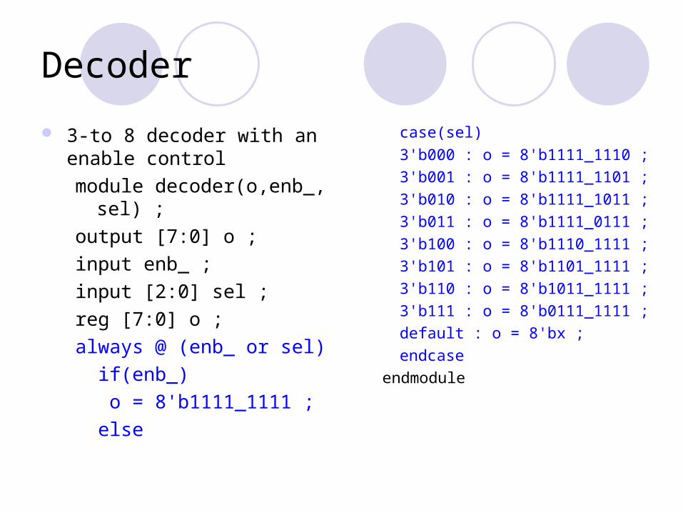
Decoder
3-to 8 decoder with an enable control
module decoder(o,enb_,sel) ;
output [7:0] o ;
input enb_ ;
input [2:0] sel ;
reg [7:0] o ;
always @ (enb_ or sel)
if(enb_)
o = 8'b1111_1111 ;
else
case(sel)
3'b000 : o = 8'b1111_1110 ;
3'b001 : o = 8'b1111_1101 ;
3'b010 : o = 8'b1111_1011 ;
3'b011 : o = 8'b1111_0111 ;
3'b100 : o = 8'b1110_1111 ;
3'b101 : o = 8'b1101_1111 ;
3'b110 : o = 8'b1011_1111 ;
3'b111 : o = 8'b0111_1111 ;
default : o = 8'bx ;
endcase
endmodule
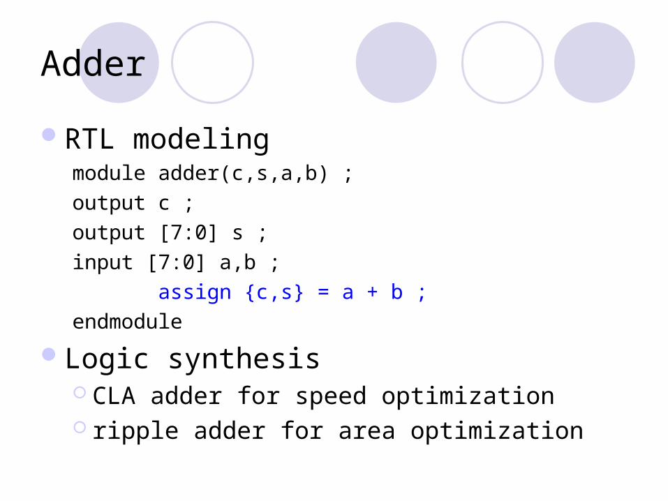
Adder
RTL modelingmodule adder(c,s,a,b) ;
output c ;
output [7:0] s ;
input [7:0] a,b ;
assign {c,s} = a + b ;
endmodule
Logic synthesis CLA adder for speed optimization ripple adder for area optimization
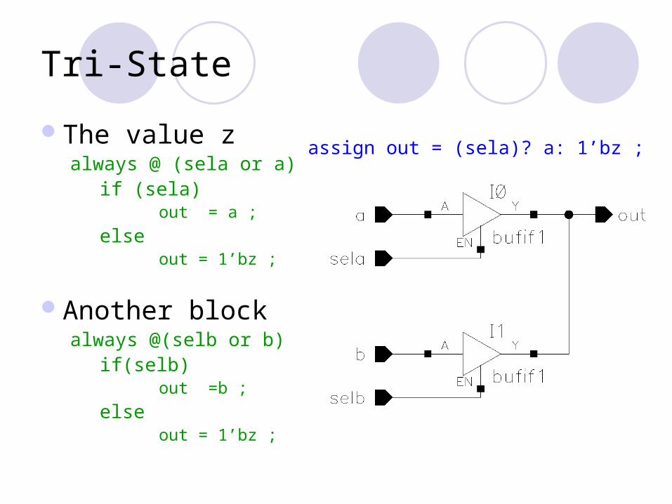
Tri-State
The value zalways @ (sela or a)
if (sela)out = a ;
elseout = 1’bz ;
Another blockalways @(selb or b)
if(selb)out =b ;
elseout = 1’bz ;
assign out = (sela)? a: 1’bz ;
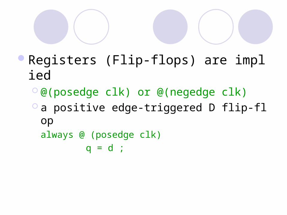
Registers (Flip-flops) are implied @(posedge clk) or @(negedge clk) a positive edge-triggered D flip-flop
always @ (posedge clk)
q = d ;

Procedural Assignments
Blocking assignments always @(posedge clk) begin
rega = data ;
regb = rega ;
end
Non-blocking assignmentsalways @(posedge clk) begin
regc <= data ;
regd <= regc ;
end
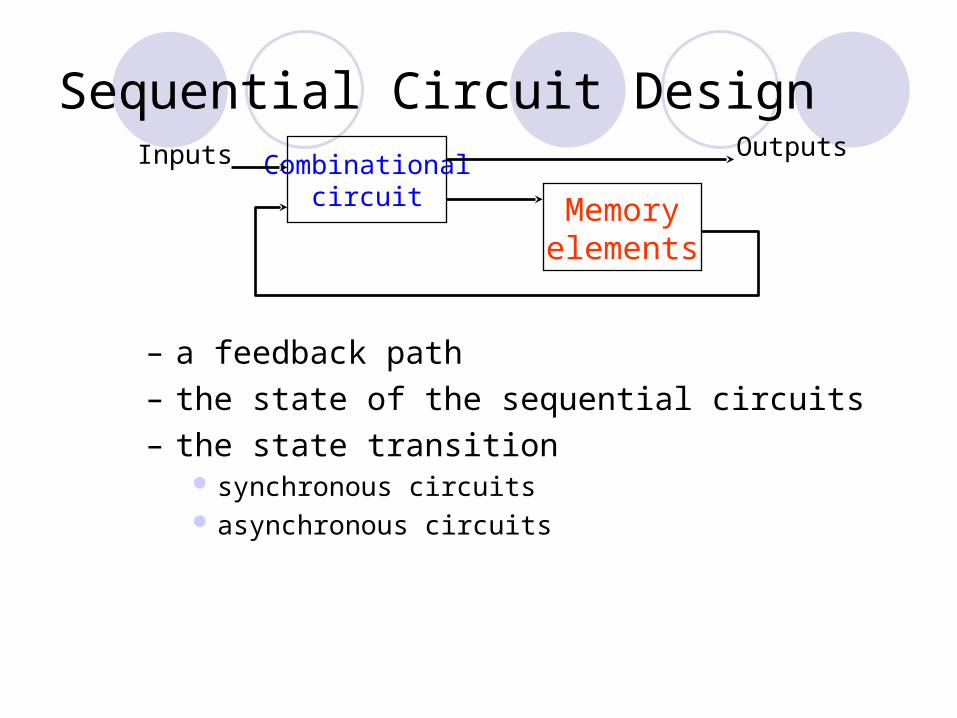
Sequential Circuit Design
– a feedback path
– the state of the sequential circuits
– the state transition synchronous circuits asynchronous circuits
Memoryelements
Combinationalcircuit
Inputs Outputs

Examples D flip-flop D latch register shifter counter pipeline FSM

Flip-Flop
Synchronous clearmodule d_ff (q,d,clk,clr_) ;output q ;input d,clk,clr_ ;reg q ;always @ (posedge clk) if (~clr_) q = 0 ; else q = d ;endmodule
Asynchronous clearalways @ (posedge clk or negedge clr_) if (~clr_) q = 0 ; else q = d ;
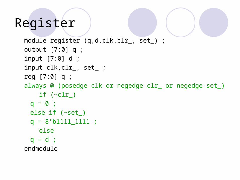
Registermodule register (q,d,clk,clr_, set_) ;
output [7:0] q ;
input [7:0] d ;
input clk,clr_, set_ ;
reg [7:0] q ;
always @ (posedge clk or negedge clr_ or negedge set_)
if (~clr_)
q = 0 ;
else if (~set_)
q = 8’b1111_1111 ;
else
q = d ;
endmodule

D Latches
D latchalways @ (enable or data)
if (enable)
q = data ;
D latch with gated asynchronous dataalways @ (enable or data or gate)
if (enable)
q = data & gate ;

D latch with gated ‘enable’always @ (enable or d or gate)
if (enable & gate)
q = d ;
D latch with asynchronous resetalways @ (reset or data or gate)
if (reset)
q = 1’b0
else if(enable)
q = data ;

Shifter
module shifter (so,si,d,clk,ld_,clr_) ;output so ;input [7:0] d ;input si,clk,ld_,clr_ ; // asynchronous clear and synchronous loadreg [7:0] q ;assign so = q[7] ;always @ (posedge clk or negedge clr_) if (~clr_)
q = 0 ; else if (~ld_)
q = d ; else
q[7:0] = {q[6:0],si} ;endmodule
shifterso
clk
si
dld_

Counter
module bcd_counter(count,ripple_out,clr,clk) ;output [3:0] count ;output ripple_out ;reg [3:0] count ;input clr,clk ;wire ripple_out = (count == 4'b1001) ? 0:1 ; // combinationalalways @ (posedge clk or posedge clr) // combinational + sequential
if (clr) ;count = 0 ;
else if (count == 4'b1001)count = 0 ;
elsecount = count + 1 ;
endmodule

Memory
module memory (data, addr, read, write);
input read, write;
input [4:0] addr;
inout [7:0] data;
reg [7:0] data_reg;
reg [7:0] memory [0:8'hff];
parameter load_file = "cput1.txt";
assign data = (read) ? memory [addr] : 8'hz;
always @ (posedge write)
memory[addr] = data;
initial
$readmemb (load_file, memory);
endmodule
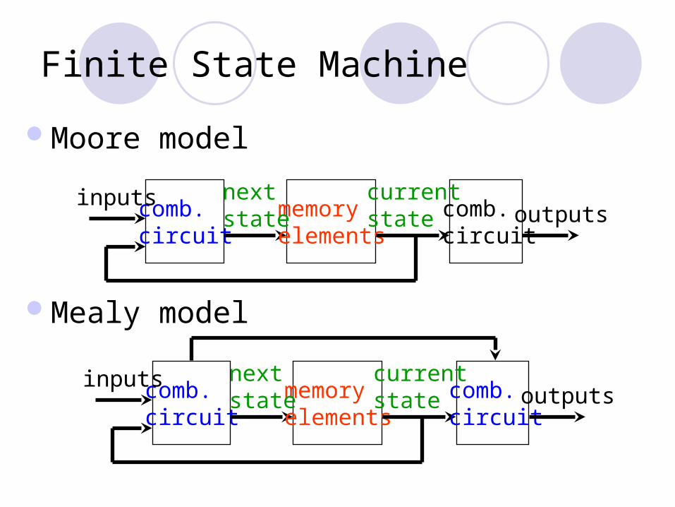
Finite State Machine
Moore model
Mealy model
comb.circuit
inputs memoryelements
nextstate comb.
circuitoutputs
currentstate
comb.circuit
inputs memoryelements
nextstate comb.
circuitoutputs
currentstate

Inefficient Description
module count (clock, reset, and_bits, or_bits, xor_bits);input clock, reset;output and_bits, or_bits, xor_bits;reg and_bits, or_bits, xor_bits;reg [2:0] count; always @(posedge clock) begin
if (reset) count = 0;
else count = count + 1; and_bits = & count; or_bits = | count; xor_bits = ^ count;
endendmodule

Six implied registers
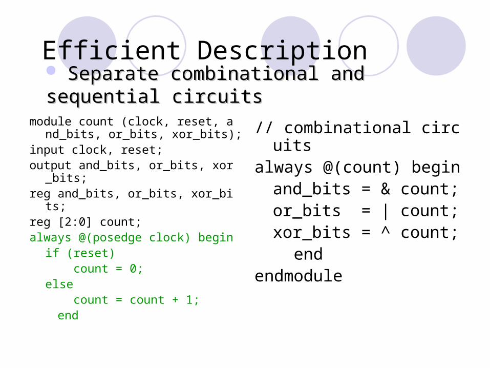
Efficient Description
module count (clock, reset, and_bits, or_bits, xor_bits);
input clock, reset;output and_bits, or_bits, xor_bits;reg and_bits, or_bits, xor_bits;reg [2:0] count;always @(posedge clock) begin
if (reset) count = 0;else count = count + 1;
end
// combinational circuitsalways @(count) begin
and_bits = & count;or_bits = | count;xor_bits = ^ count;
endendmodule
Separate combinational and sequential circuitsSeparate combinational and sequential circuits
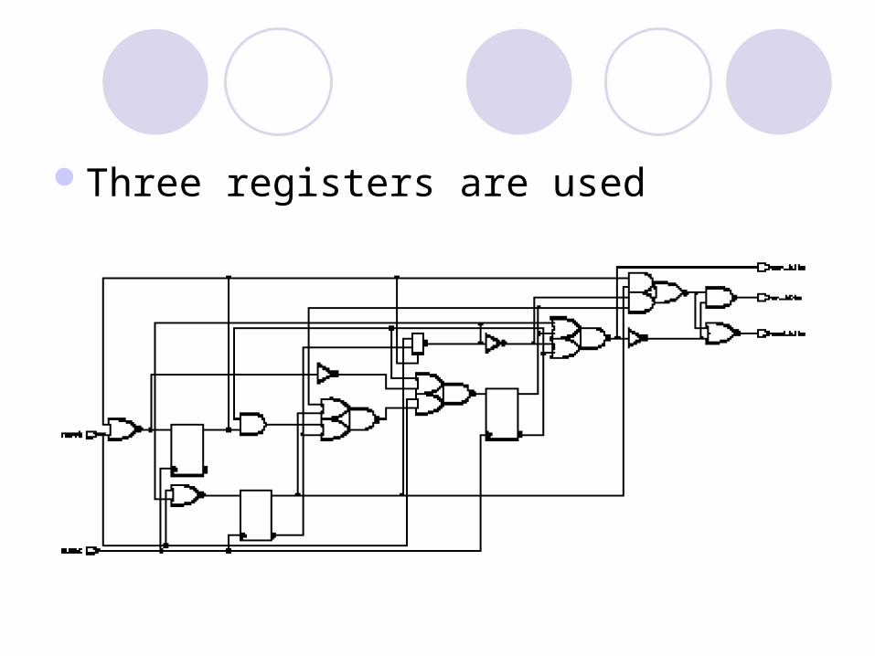
Three registers are used

Mealy Machine Examplemodule mealy (in1, in2, clk, reset,out);input in1, in2, clk, reset;output out;reg current_state, next_state, out;// state flip-flops always @(posedge clk or negedge re
set) if (!reset)
current_state = 0; else
current_state = next_state;// combinational: next-state and outpu
tsalways @(in1 or in2 or current_state) case (current_state)
0: beginnext_state = 1;out = 1'b0;
end1: if (in1) begin
next_state = 1'b0;out = in2;
end else begin
next_state = 1'b1;out = !in2;
end endcaseendmodule
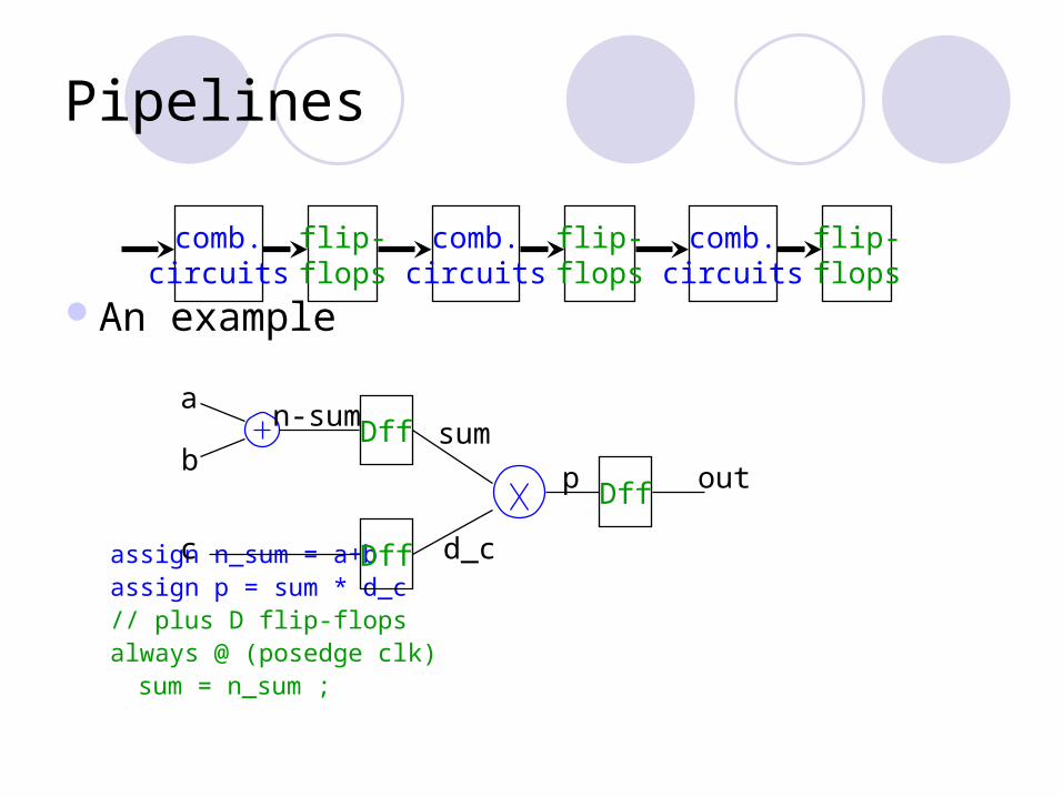
Pipelines
An example
assign n_sum = a+bassign p = sum * d_c// plus D flip-flopsalways @ (posedge clk)
sum = n_sum ;
flip-flops
comb.circuits
flip-flops
comb.circuits
flip-flops
comb.circuits
Dff
Dff
Dff
a
b
c
out
n-sumsum
d_c
p

Traffic Light Controller
Picture of Highway/Farmroad Intersection:
Highway
Highway
Farmroad
Farmroad
HL
HL
FL
FL
C
C
A FSM Example

Traffic Light Controller? Tabulation of Inputs and Outputs:
Input SignalresetCTSTL
Output SignalHG, HY, HRFG, FY, FRST
Descriptionplace FSM in initial statedetect vehicle on farmroadshort time interval expiredlong time interval expired
Descriptionassert green/yellow/red highway lightsassert green/yellow/red farmroad lightsstart timing a short or long interval
? Tabulation of Unique States: Some light configuration imply others
StateS0S1S2S3
DescriptionHighway green (farmroad red)Highway yellow (farmroad red)Farmroad green (highway red)Farmroad yellow (highway red)
Specifications
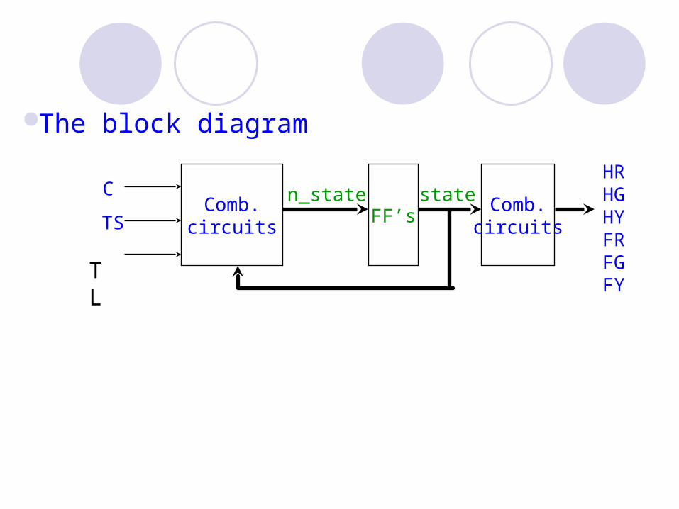
TL
FF’sComb.circuits
Comb.circuits
staten_stateC
TS
The block diagram
HRHGHYFRFGFY
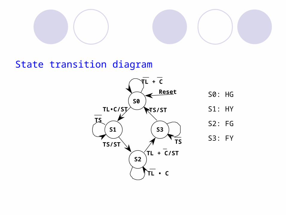
State transition diagram
S0: HG
S1: HY
S2: FG
S3: FY
Reset
TL + C
S0TL•C/ST
TS
S1 S3
S2
TS/ST
TS/ST
TL + C/ST
TS
TL • C

Verilog Description
module traffic_light(HG, HY, HR, FG, FY, FR,ST_o,tl, ts, clk, reset, c) ;
output HG, HY, HR, FG, FY, FR, ST_o;input tl, ts, clk, reset, c ;reg ST_o, ST ;reg[0:1] state, next_state ;parameter EVEN= 0, ODD=1 ;parameter S0= 2'b00, S1=2'b01, S2=2'b10, S3=2'b11;assign HG = (state == S0) ;assign HY = (state == S1) ;assign HR = ((state == S2)||(state == S3)) ;assign FG = (state == S2) ;assign FY = (state == S3) ;assign FR = ((state == S0)||(state == S1)) ;

// flip-flops
always@ (posedge clk or posedge reset)
if(reset) // an asynchronous reset
begin
state = S0 ;
ST_o = 0 ;
end
else
begin
state = next_state ;
ST_o = ST ;
end

always@ (state or c or tl or ts)
case(state) // state transition
S0:
if(tl & c)
begin
next_state = S1 ;
ST = 1 ;
end
else
begin
next_state = S0 ;
ST = 0 ;
end
Reset
TL + C
S0TL•C/ST
TS
S1 S3
S2
TS/ST
TS/ST
TL + C/ST
TS
TL • C

S1:if (ts) begin
next_state = S2 ;ST = 1 ;
endelse begin
next_state = S1 ;ST = 0 ;
end S2:
if(tl | !c) beginnext_state = S3 ;ST = 1 ;
endelse begin
next_state = S2 ;ST = 0 ;
end
Reset
TL + C
S0TL•C/ST
TS
S1 S3
S2
TS/ST
TS/ST
TL + C/ST
TS
TL • C
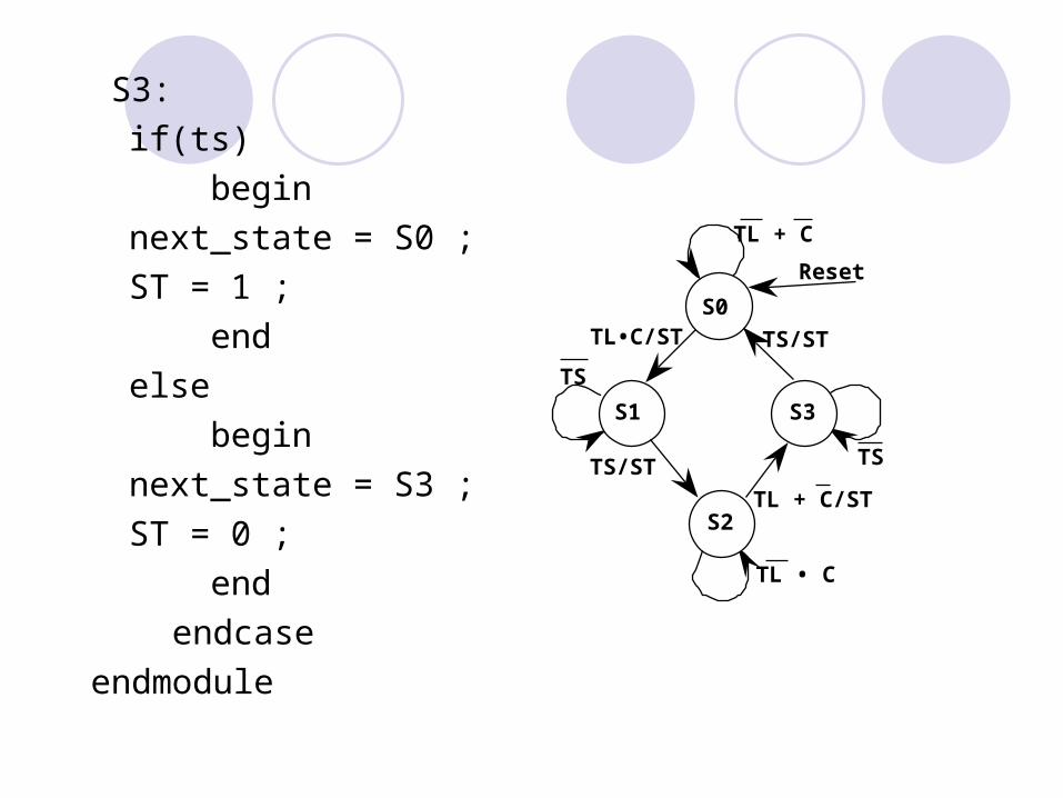
S3:
if(ts)
begin
next_state = S0 ;
ST = 1 ;
end
else
begin
next_state = S3 ;
ST = 0 ;
end
endcase
endmodule
Reset
TL + C
S0TL•C/ST
TS
S1 S3
S2
TS/ST
TS/ST
TL + C/ST
TS
TL • C
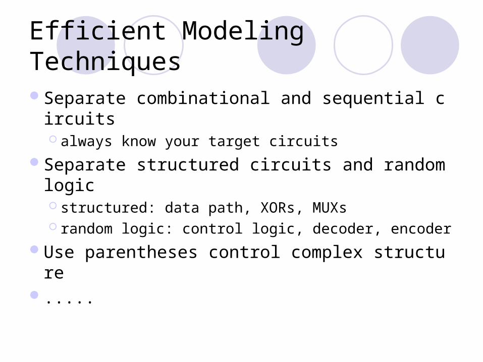
Efficient Modeling Techniques
Separate combinational and sequential circuits always know your target circuits
Separate structured circuits and random logic structured: data path, XORs, MUXs random logic: control logic, decoder, encoder
Use parentheses control complex structure.....
Some main points to remember
Verilog is concurrent
Think while writing your program.
Blocking and Non-blocking Code
Conclusions
Verilog modeling structured modeling continuous assignment RTL modeling
Design digital systems separate combinational and sequential descripti
on always keep your target circuits in mind
Reference
Verilog-XL Training Manual, CICLogic Synthesis Design Kit, CICHDL Compiler for Verilog Reference Manu
al, SynopsysSynthesis Application Notes, Synopsys On
line DocumentationDigital System Design Using Verilog, Min
g-Feng Chang, CSIE, NUTU