chapter 3. gate-level minimizationtioh.weebly.com/uploads/2/5/4/3/25433593/mano_ch03_ti.pdf ·...
TRANSCRIPT

Digital Design, Kyung Hee Univ.
1
Chapter 3. Gate-Level Minimization
Tong In Oh
Digital Design, Kyung Hee Univ.
2
Chapter 3. Gate-Level Minimization• Finding an optimal gate-level implementation of the Boolean functions
describing a digital circuit• Difficult to execute by manual methods• Computer-based logic synthesis tools• Important to understand the underlying mathematical description and
solution of the problem• Execute a manual design of simple circuits
Digital Design, Kyung Hee Univ.
3
3.2 Map Method• Complexity of the algebraic expression in many different forms but
equivalent• Algebraic means – lack specific rules• Karnaugh Map (K-map) method – simple, straightforward procedure
for minimizing Boolean functions• Pictorial form of a truth table• K-map
• Diagram made up of squares• Each square representing one minterm of the function• Function = Sum of minterms• Present a visual diagram of all possible ways a function • Standard forms: sum of products or product of sums• The simplest expression (not unique)

Digital Design, Kyung Hee Univ.
4
Two Variable K-Map• Four minterms for two variables• Mark the squares whose minterms belong to a given function
FIGURE 3.1 Two-variable K-map FIGURE 3.2 Representation of functions in the map

Digital Design, Kyung Hee Univ.
5
Three Variable K-Map• Eight minterms for three binary variables• Similar to the Gray code (only one bit changes in value from one
adjacent column to the next)• Mark the squares whose minterms belong to a given function
FIGURE 3.3 Three-variable K-map

Digital Design, Kyung Hee Univ.
6
Example 3.1
FIGURE 3.4 Map for Example 3.1, F(x, y, z) = Σ(2, 3, 4, 5) = x’y + xy’
Digital Design, Kyung Hee Univ.
7
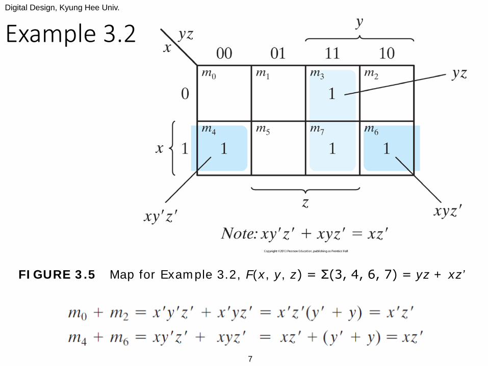
Example 3.2
FIGURE 3.5 Map for Example 3.2, F(x, y, z) = Σ(3, 4, 6, 7) = yz + xz’

Digital Design, Kyung Hee Univ.
8
Example 3.3
FIGURE 3.6 Map for Example 3.3, F(x, y, z) = Σ(0, 2, 4, 5, 6) = z’ + xy’

Digital Design, Kyung Hee Univ.
9
Example 3.4
FIGURE 3.7 Map of Example 3.4, A’C + A’B + AB’C + BC = C + A’B

Digital Design, Kyung Hee Univ.
10
3.3 Four-Variable K-Map
FIGURE 3.8 Four-variable map

Digital Design, Kyung Hee Univ.
11
Example 3.5
FIGURE 3.9 Map for Example 3.5, F(w, x, y, z) = Σ(0, 1, 2, 4, 5, 6, 8, 9, 12, 13, 14) = y’ + w’z’ + xz’

Digital Design, Kyung Hee Univ.
12
Example 3.6
FIGURE 3.10 Map for Example 3.6, A’B’C’ + B’CD’ + A’BCD’ + AB’C’ = B’D’ + B’C’ + A’CD’
Digital Design, Kyung Hee Univ.
13
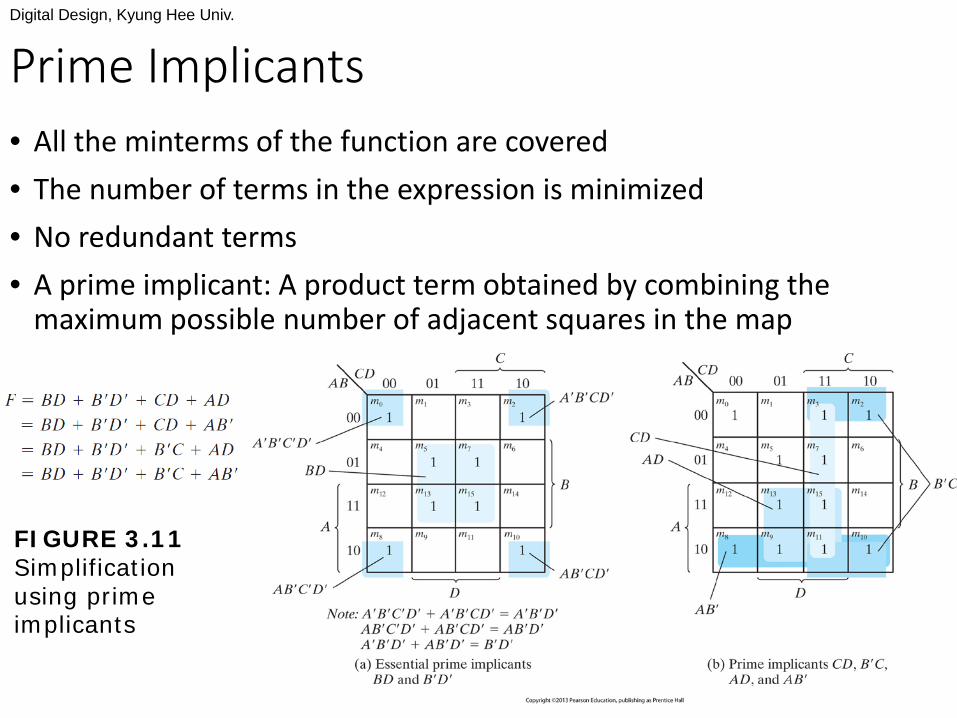
Prime Implicants• All the minterms of the function are covered• The number of terms in the expression is minimized• No redundant terms• A prime implicant: A product term obtained by combining the
maximum possible number of adjacent squares in the map
FIGURE 3.11Simplification using prime implicants

Digital Design, Kyung Hee Univ.
14
3.4 Product of Sums Simplification
FIGURE 3.12 Map for Example 3.7, F(A, B, C, D) = Σ(0, 1, 2, 5, 8, 9, 10) = B’D’ + B’C’ + A’C’D = (A’ + B’)(C’ + D’)(B’ + D)

Digital Design, Kyung Hee Univ.
15
Gate-Level Implementation

Digital Design, Kyung Hee Univ.
16
3.5 Don’t Care Conditions• Function is not specified for certain combinations of the variables• = Incompletely specified functions• Don’t care condition = unspecified minterms of a function• Further simplification• Marked as X
FIGURE 3.15Example with don’t-care conditions

Digital Design, Kyung Hee Univ.
17
3.6 NAND/NOR Implementation• Easier to fabricate with electronic components• Basic gates used in all IC digital logic families• NAND circuits = Universal gate• To obtain the simplified Boolean function in terms of Boolean
operators and then convert the function to NAND logic
FIGURE 3.16 Logic operations with NAND gatesFIGURE 3.17 Two graphic symbols for a three-input NAND gate

Digital Design, Kyung Hee Univ.
18
Two-Level Implementation• The implementation of Boolean functions with NAND gates requires
that the functions be in sum-of-products form.
FIGURE 3.18 Three ways to implement F = AB + CD

Digital Design, Kyung Hee Univ.
19
Example 3.9
FIGURE 3.19 Solution to Example 3.9

Digital Design, Kyung Hee Univ.
20
Multilevel NAND Circuits• F=A(CD+B)+BC’• Converting a multilevel AND-OR diagram into an all-NAND diagram
FIGURE 3.20 Implementing F = A(CD + B) + BC’

Digital Design, Kyung Hee Univ.
21
FIGURE 3.21 Implementing F = (AB’ + A’B) (C + D’)

Digital Design, Kyung Hee Univ.
22
NOR Implementation• Dual of the NAND operation = Universal gate• Converting OR-AND diagram to a NOR diagram• Product of sums
FIGURE 3.22 Logic operations with NOR gates FIGURE 3.23 Two graphic symbols for the NOR gate

Digital Design, Kyung Hee Univ.
23
FIGURE 3.24 Implementing F = (A + B)(C + D)E
FIGURE 3.25 Implementing F = (AB’ + A’B)(C + D’) with NOR gates

Digital Design, Kyung Hee Univ.
24
3.7 Other Two-Level Implementations• NAND and NOR gates• Allow the possibility of a wire connection between the outputs of two
gates to provide a specific logic function = wired logic• Wired-AND logic: open-collector TTL NAND
• Wired-OR logic: NOR outputs of ECL gates
FIGURE 3.26 Wired logic: (a) Wired-AND logic with two NAND gates (b) Wired-OR in emitter-coupled logic (ECL) gates

Digital Design, Kyung Hee Univ.
25
Nondegenerate Forms (1)• Two-level combinations of gates• AND/OR/NAND/NOR• Degenerate forms: single operation• Nondegenerate forms: implementation in
• Sum-of-products form• Product-of-sums form• AND-OR-INVERT Implementation: NAND-AND, AND-NOR: Wired AND with NAND
FIGURE 3.27 AND–OR–INVERT circuits, F = (AB + CD + E )’

Digital Design, Kyung Hee Univ.
26
Nondegenerate Forms (2)• OR-AND-INVERT Implementation: OR-NAND, NOR-OR: Wired OR with NOR
FIGURE 3.28 OR–AND–INVERT circuits, F = [(A + B )(C + D)E]’

Digital Design, Kyung Hee Univ.
27
Tabular Summary and Example
Digital Design, Kyung Hee Univ.
28
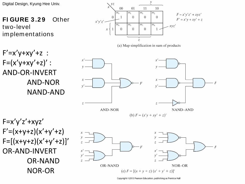
FIGURE 3.29 Other two-level implementations
F’=x’y+xy’+z : F=(x’y+xy’+z)’ : AND-OR-INVERT
AND-NORNAND-AND
F=x’y’z’+xyz’F’=(x+y+z)(x’+y’+z)F=[(x+y+z)(x’+y’+z)]’OR-AND-INVERT
OR-NANDNOR-OR
Digital Design, Kyung Hee Univ.
29
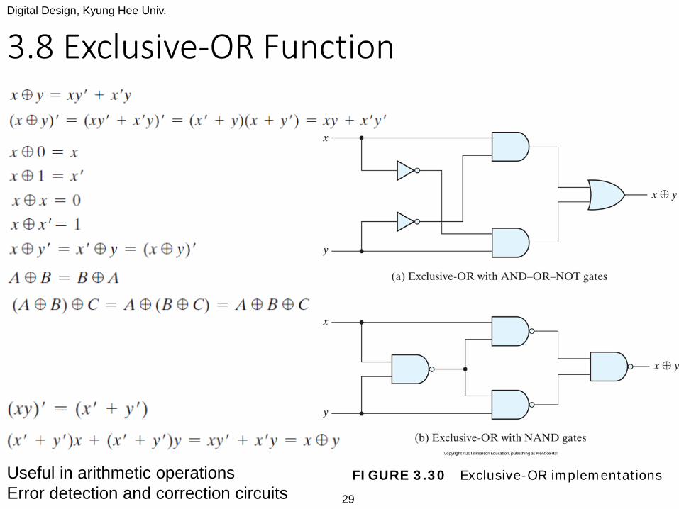
3.8 Exclusive-OR Function
FIGURE 3.30 Exclusive-OR implementationsUseful in arithmetic operationsError detection and correction circuits

Digital Design, Kyung Hee Univ.
30
Odd Function• Multiple-variable exclusive-OR operation• Odd number of variables be equal to 1 = odd function
FIGURE 3.31 Map for a three-variable exclusive-OR function
FIGURE 3.32 Logic diagram of odd and even functions

Digital Design, Kyung Hee Univ.
31
Four-variable Exclusive OR Operation
FIGURE 3.33 Map for a four-variable exclusive-OR function

Digital Design, Kyung Hee Univ.
32
Parity Generation and Checking