thermal parameter estimation using recursive identification
TRANSCRIPT

228 IEEE TRANSACTIONS ON POWER ELECTRONICS. VOL 6. NO 2, APRIL 1991
Thermal Parameter Estimation Using Recursive Identification
Gary L. Skibinski and William A. Sethares, Member, IEEE
Abstract-A novel method that converts a semiconductor transient thermal impedance curve (TTIC) into an equivalent thermal RC net- work model is presented. Thermal resistance ( R ) and thermal capac- itance ( C ) parameters of the model are identified using manufacturer's data and off line recursive least square (RLS) techniques. Relevant estimation theory concepts and the formulation of an appropriate model for the identification process are given. Model synthesis is illustrated using an isolated base power transistor module. The application of time decoupled theory for high order thermal models is outlined. Simula- tion of junction temperature responses using model and manufacturer TTIC's are compared. Estimated parameter validity is further con- firmed by parameter calculation obtained from module physical di- mensions.
I . INTRODUCTION OWER converter manufacturers typically utilize the rela- P tively low but significant thermal heat capacity of power
semiconductors to obtain short duration overload ratings well in excess of continuous ratings. The methods for determining the peak allowable junction temperature { (max) } under tran- sient and intermittent loading are well established and have re- mained essentially unchanged since 1959 [ I]. The standard approach uses the TTIC supplied by device manufacturers (Fig. l(a)). Junction temperature response to device power pulses are estimated from this curve and the principle of superposition for conditions such as single pulse overload, repetitive pulse over- load, overloads following continuous duty and irregularly shaped power versus time profiles. Indeed, power transistor safe operating area (SOA) limits are usually based upon this ap- proach [2]-[5]. However, transient junction temperature esti- mation using the TTIC approach has several shortcomings.
1 ) a-posteriori Calculations: Circuit simulation programs containing sophisticated device models exist that can calculate instantaneous power versus time profiles [6]-[7]. However, in- stantaneous junction temperature vs. time profiles cannot be solved with the TTIC concept until the entire overload simula- tion process is complete, stored in memory and broken down into equivalent pulse amplitude and durations. This inefficiency suggests the use of a device thermal model (Fig. l(b) and (c)) for maximizing simulation capability by solving both the elec- trical and thermal network models simultaneously.
2) Graphical Analysis: The standard TTIC approach re- quires cumbersome graphical analysis to transform the irregu- larly shaped power profiles, such as the switching and conduction loss profiles in SOA calculations, into equivalent energy [W-s] square power pulses upon which this curve is based.
Manuscript received July 2 3 , 1990. The authors are with the University of Wisconsin-Madison. 1415 John-
son Drive, Madison, W1 53706. IEEE Log Number 9042335.
xu 10-4 Io-
Time [seconds]
A Ojc Model
(c)
Fig. I . (a) Semiconductor transient Thermal Impedance curve (junction- case). (b) Estimated Black Box Model of Fig. I(a). (c) Thermal Model Structure of Fig. I(a) and (b).
3) Repeat Calculations: Each application of a new overload sequence requires Tj to be recalculated.
4) Desired Accuracy: The accuracy of estimated junction temperatures decreases for increasingly complex overload waveforms such as pulse width modulation (PWM) acceleration of a motor. When using the standard approach, gross simpli- fying assumptions are necessary to keep graphical analysis and hand computations tractable.
0885-8993/91/0400-0228$0l .OO 0 1991 IEEE
SKIBINSKI AND SETHARES: THERMAL PARAMETER ESTIMATION USING RECURSIVE IDENTIFICATION
The shortcomings of the standard approach suggest the need to develop an accurate thermal model to make better estimates of T,. Use of a device thermal model for indirect measurement of the junction to case temperature rise { A Tjc } may result in improved converter fault diagnostics. Indirectly calculating A Tjc in real time may be done with the discrete transfer func- tion model of Fig. l(b) and a Digital Signal Processor (DSP)/ microprocessor or an analog operational amplifier model of Fig. l(c). In addition, potential advantages in substantially in- creased converter overload ratings exist when using the A Tjc observer based model in real time adaptive control [8].
In this paper, a new approach to the problem of determining device thermal characteristics is presented from the system identification point of view [9]. Sections I1 and I11 outline the basic identification procedure used and the governing laws for device thermal model building. Sections IV and V review and apply estimation theory principles to determine the RC param- eter values given the manufacturer’s TTIC curve. Section VI presents identification results for an isolated base transistor model example and discusses parameter accuracy of the iden- tified RC values.
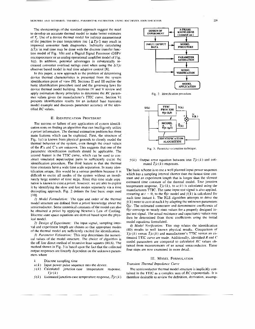
11. IDENTIFICATION PROCEDURE
The success or failure of any application of system identifi- cation rests on finding an algorithm that can intelligently utilize a priori information. The thermal estimation problem has three main features which can be exploited. First, the structure of Fig. l(c) is known from physical grounds to closely model the thermal behavior of the system, even though the exact values of the R’s and C’s are unknown. This suggests that one of the parametric identification methods should be applicable. The second feature is the TTIC curve, which can be used to con- struct simulated input/output pairs to sufficiently excite the identification procedure. The third feature is that the thermal time constants have a wide time scale separation. In many iden- tification setups, this would be a serious problem because it is difficult to excite all modes of the system without an inordi- nately large number of time steps. Since this time scale sepa- ration is known to exist apr ior i , however, we are able to exploit i t by identifying the slow and fast modes separately via a time decoupling approach. Fig. 2 defines the four basic steps used
I ) Model Formulation: The type and order of the thermal model structure are defined from a priori knowledge about the semiconductor. Some numerical constants of the model can also be obtained a priori by applying Newton’s Law of Cooling. Discrete state space equations are derived based upon the phys- ical model.
2 ) Design of Experiment: The input signal, sampling inter- val and experiment length are chosen so that approprate modes of the thermal model are sufficiently excited for identification.
3) Parameter Estimation: This step determines the numeri- cal values of the model structure. The choice of algorithm is the off-line direct method of recursive least squares (RLS). The method shown in Fig. 3 is based upon the fact that the collected output responses are linearly dependent on the unknown param- eters where
1101.
k Discrete sampling time U ( k ) Input power pulse sequence into the device. y ( k ) Calculated junction-case temperature response,
y ( k ) Estimated junction-case temperature response: f j c ( k ) T j c ( k )
A-PRIORI KNOWLEDGE ( intended use )
DESIGN OF EXPERIMENT
t + MODEL INPUT / OUTPUT
DATA STRUCTURE
PARAMETER ESTIMATION
VERIFICATION
I [ MODEL APPLICATION
Fig. 2 . Identification procedure
I / IDENTIFICATION ~ 4-1
229
Fig. 3. Parameter estimation technique.
j ( k ) Output eyor equation between true T j c ( k ) and esti-
The basic scheme is to use a well planned input power sequence which has a sampling interval shorter than the fastest time con- stant and an experiment length that is longer than the slowest estimated time constant of the thermal model. True junction temperature response, T j c ( k ) , to u ( k ) is calculated using the manufacturers TTIC. The 5ame input test signal is also applied, restarting at t = 0, to the ejc model and j ( k ) is calculated for each time instant k . The RLS algorithm attempts to drive the E( k ) error to zero at each k by adapting the unknown parameters e j c . The estimated numerator and denominator coefficients of e jc converge to steady state values for a properly designed in- put test signal. The actual resistance and capacitance values may then be determined from these coefficients using the initial model equations formulated.
4) Model VeriJication: This step relates the identification (ID) results to well known physical results. Comparison of T j c ( k ) versus f j c ( k ) and manufacturer’s TTIC versus an es- timated TTIC curve are made. Additionally, identified R and C model parameters are compared to calculated RC values ob- tained from measurements of an actual semiconductor. These four steps are now examined in more detail.
mated Tjc ( k ) responses.
111. MODEL FORMULATION Transient Thermal Impedance Curve
The semiconductor thermal model structure is implicitly con- tained in the TTIC as a complex sum of RC exponentials. It is therefore desirable to review the definition, derivation, assump-

230 IEEE TRANSACTIONS ON POWER ELECTRONICS, VOL. 6, NO. 2 , APRIL 1991
tions and application of this curve. The concept of thermal re-
systems with temperature ["C], heat flow due to power dissi- (a) Power Device P1 p2 trL.. sistance is based upon an analogy between electrical and thermal
pation [watts] and thermal resistance [ "C/W ] being analogous to voltage, current and electrical resistance [ l l ] . The TTIC in Fig. l(a) is obtained by applying a single square power pulse P1 to the device until the junction temperature reaches steady state at time tss. Junction temperature rise { A Tjc } is deter- mined by fixing the case constant at ambient temperature { Tc = T u } and measuring device temperature with infrared meth- ods or electrical temperature sensitive parameters { TSP} such as forward voltage drop {V'} or base emitter voltage { V b e }
change in Vbe ( G 2 mv/"C/junction) versus time to a pre-
base current. The transient thermal impedance is defined at any time I as
P2 (b) Equivalent
Device Power
time
[ 121. The actual A Tjc rise is found by correlating the measured - PI vious Vbe temperature test for constant and Fig, 4. (a) Device power profile versus time. (b) Equivalent heating and
cooling pulses.
(1) T j ( t ) - Tc( t ) A T j c ( t ) -- -
P1 P1 . 0 j c ( t ) =
The thermal system is assumed to be linear, and hence super- position can be applied to the TTIC. The TTIC is a step re- sponse curve with zero initial conditions, relating device step input power to ATjc at the output. The power profile in Fig. 4(a) can be separated into equivalent heating and cooling pulse durations of t x and t y as shown in Fig. 4(b). The junction tem- perature rise can be determined by adding individual Tjc pulse responses [ 11 :
A T j c ( t , ) = P1 * 0jc(t,) (2 1 ATjc( t2) = P1 * e jc( t2) - P1 * 0jc(tz - t l )
+ P 2 * 0jC(t, - t , ) . (3)
The published TTIC is usually higher than the tested value to account for manufacturing variations and the increase in ther- mal resistance over time.
a-priori Knowledge
Knowledge of the physical properties of the semiconductor can be used to fix the model structure and order, and to deter- mine some numerical values of the Black Box shown in Fig. l(c). The use of all available a priori knowledge prior to ap- plication of the identification algorithm is important since mis- leading results due to an assumed wrong structure are difficult to detect from data alone. Also, a priori knowledge can en- hance model validity and model accuracy. An appropriate model can be formulated using 1) physical knowledge, 2) I/O mea- surements, or both.
1) Physical Knowledge: The model order is dependent on the type of semiconductor package used as shown in Fig. 5. The exact order can be determined by visual inspection of the package cross sectional view and replacing significant heat ca- pacity materials ( C u , Si , M O ) with thermal capacitances. The number of capacitors determines the model order. One dimen- sional heat flow from junction to case results in the typical RC network structure shown in Fig. l(c). Numerical values for R5 and C4 of the copper base can be obtained without package dis- assembly by applying the governing thermal laws defined in Appendix I to a 4th order 50-A isolated base transistor:
R, = L , / ( K * A e ) [ "C/W] (4)
c, = p * c p * v [W-S/"C]. ( 5 )
I SOLDER I
(d) Fig. 5. Model order dependent on semiconductor package. (a) Direct bonded copper process [2nd order]. (b) T03/T0220/stud type [3rd order]. (c) Compression bonded thyristor [4th order]. (d) Isolated base transistor module [4th order].
Thermal resistance and capacitance calculations can be ex- tended to Rl-R4 and Cl-C3 by disassembling the package and physically measuring each material thickness and cross section area perpendicular to heat flow. This calculated parameter ap- proach is documented in Appendix I with the results shown in Table I. An analog simulation of this RC structure is plotted in Fig. 6 versus the actual TTIC. This procedure alone may pro- duce sufficient B j c ( t ) accuracy for the intended use of the model.
2 ) U0 Measurement: The asymptotic behavior at the origin and steady state time tss of the manufacturer's TTIC in Fig. 6 can provide numerical values for parameters R1, Cl and for the
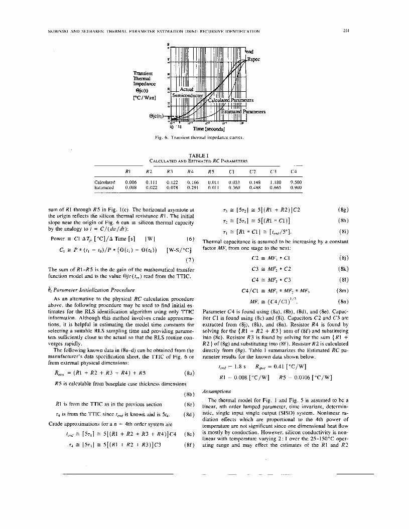
SKIBINSKI AND SETHARES: THERMAL PARAMETER ESTIMATION USING RECURSIVE IDENTIFICATION 23 1
Transient Thermal Impadance
W t ) ["Cl Watt]
Qjc
"' Time [seconds] Fig. 6. Transient thermal impedance curves.
TABLE I CALCULATED AND ESTIMATED RC PARAMETERS
R1 R2 R3 R4 R5 C1 c 2 c 3 c 4
Calculated 0.006 0.111 0.122 0.166 0.011 0.033 0.148 1.180 9.500 Estimated 0.008 0.022 0.078 0.291 0.011 0.360 0.488 0.665 0.900
sum of R1 through R 5 in Fig. l(c). The horizontal asymtote at the origin reflects the silicon thermal resistance R1. The initial slope near the origin of Fig. 6 can E silicon thermal capacity by the analogy to i = C/(dv/dt):
Power z Cl AT,< [ OC]/A Time [s] [W] ( 6 )
[ w - s / "C ]
( 7 )
cI s P * ( t l - t , , ) /~ * (e@,) - e(t,))
The sum of R1-R5 is the dc gain of the mathematical transfer function model and is the value €ljc(rsy) read from the TTIC.
8, Parameter Initialization Procedure
As an alternative to the physical RC calculation procedure above, the following procedure may be used to find initial es- timates for the RLS identification algorithm using only TTIC information. Although this method involves crude approxima- tions, it is helpful in estimating the model time constants for selecting a suitable RLS sampling time and providing parame- ters sufficiently close to the actual so that the RLS routine con- verges rapidly.
The following known data in (8a-d) can be obtained from the manufacturer's data specification sheet, the TTIC of Fig. 6 or from external physical dimensions:
RJprr = (R1 + R2 + R3 + R 4 ) + R5 (sa)
R5 is calculable from baseplate case thickness dimensions
(8b)
(8c) R1 is from the TTIC as in the previous section
r4 is from the TTIC since rrnd is known and is 9,. (8d) Crude approximations for a n = 4th order system are
tc,,ld = [5r4] = 5 [ ( R 1 + R2 + R3 + R 4 ) ] C 4 (8e)
r4 G [5r3] G 5 [ ( R 1 + R2 + R 3 ) ] C 3 (8 f )
r, E [5r2] z 5 [ ( R 1 + R 2 ) ] C 2
r2 E [5r , ] E 5 [ ( R 1 * C l ) ]
7, E [ R l * Cl] E [rCnd/5"].
(8g)
(8h)
(8i)
Thermal capacitance is assumed to be increasing by a constant factor MF, from one stage to the next:
C 2 E MF, * C1
C 3 E MF, * C 2
C 4 E MF, * C 3
(8j)
(8k)
(81)
(8m) C 4 / C 1 E MF, * MF, * MF,
MF, E ( C 4 / C 1 ) 1 ' 3 . (8n)
Parameter C 4 is found using @a), (8b), (8d), and (8e). Capac- itor C1 is found using (8c) and (8i). Capacitors C 2 and C 3 are extracted from (8j), (8k), and (8n). Resistor R 4 is found by solving for the { R I + R 2 + R 3 ) sum of (8f) and substituting into (8e). Resistor R 3 is found by solving for the sum { R1 + R 2 } of (8g) and substituting into (8f). Resistor R 2 is calculated directly from (8g). Table I summarizes the Estimated RC pa- rameter results for the known data shown below.
rend = 1.8 s R,pr,c = 0.41 [ "C/W]
R1 = 0.008 ["C/W] R5 = 0.0106 ["C/W]
Assumptions
The thermal model for Fig. 1 and Fig. 5 is assumed to be a linear, nth order lumped parameter, time invariant, determin- istic, single input single output (SISO) system. Nonlinear ra- diation effects which are proportional to the 4th power of temperature are not significant since one dimensional heat flow is mostly by conduction. However, silicon conductivity is non- linear with temperature varying 2 : 1 over the 25-150°C oper- ating range and may effect the estimates of the R1 and R 2

232 IEEE TRANSACTIONS ON POWER ELECTRONICS, VOL. 6, NO. 2 , APRIL 1991
thermal resistances. Also, some insulators such as Be0 will vary by 20% over the same range. The present procedure ignores these nonlinearities, though their incorporation into the design procedure is an important area for further investigation. Lastly, measurement noises are assumed negligable.
Equations
A thermal model can be formulated using either an internal state space or I/O transfer function model approach. The first method is the most desirable since it is directly related to the physical structure of Fig. l(c). However, the need to measure the internal states (x , , x2, x3, x4) to find model coefficients pre- cludes its use. The transfer function approach must be used since only U0 data from the TTIC is available. The disadvantage of this approach is that the ejc model coefficients obtained from I/O data have no direct physical meaning. The RC parameters of the structure are hidden in the numerator and denominator coefficients and must be further extracted. The transfer function model is developed in the continuous time domain and must be further discretized for use in the identification algorithm.
Continuous State Space Model
The system equations for the 4th order structure in Fig. l(c) can be obtained using the capacitor voltages (temperatures) as the state variables (x l r x2, x3, x4). The output equation variable ( Y ) represents the silicon absolute junction temperature i",. The input variable ( U ) * represents the device power in watts. The transfer function ejc reflects the temperature rise for a given power input. It is derived by applying the Laplace transform operator { s } to (9a), solving for X and substituting into (loa):
where B = ( l / C l , 0, 0, O ) T , C = ( I , 0, 0 , O ) T , D = R,, and
A =
-1 1 R2 C1 R2 C1 ~ -
the above equation can be split into two cascaded 2nd order systems which match the dc gain and overall dynamics of the original system. Thus, only simpler 2nd order equations peed be developed using xI, x2, RI, R2, R3, C1 and C2:
/ -1 1 \
\ I \R2C2 R2C2 R3C2/
(12)
Y = [ l O]XT + [RlIP. (13)
This is the time scale decoupling, and is possible whenever the unknown system has widely separated modes. In essence, the identification of the slow modes is conducted separately from the identification of the fast modes.
Discrete Transfer Function Model
In order to utilize an appropriate identification algorithm, the continuous system (12) and (13) must be discretized for com- puter implementation. There are several possible methods such as Eulers methods, Tustins approximation, step invariance, etc. An infinite series approximation was chosen because it leads to relatively simple equations relating the RC parameters to the filter coefficients. The discrete system equations are defined using the time shift operator, { q } .
X ( k + 1) = q X ( k ) = @ X ( k ) + h ( k ) ["C/At] (14)
Y ( k ) = C X ( k ) + D u ( k ) ["C] (15)
The pulse transfer function is derived by solving (14) for x ( k ) and substituting into (15) [ 131:
e j c ( k ) = ~ ( k ) / ~ ( k ) = c(qz - + D [ o c / w ]
( 16)
0 0
0 1
R3C2
- 1 1 \ 1 0 R3 C3 (--- R3C3 R4C3) R4C3
- 1 R4 C4
0 0
The symbolic transfer function corresponding to ( 1 1) contains four numerator and four denominator coefficients in the so to s4 powers. Determination of the RC parameter values requires simultaneously solving the eight coefficient equations. Four of the eight coefficients each contain 21 nonlinear sum and product terms of the form 1 /( R, C,), which makes solution a formid- able task. Using the a priori knowledge that the values of the capacitors are widely separated in this 4th order thermal model,
where h = sample interval
CP = state transition matrix @ = eAh = I + Ah {first order approximation}
I' = j h e A ' d c B . (17)

SKIBINSKI AND SETHARES: THERMAL PARAMETER ESTIMATION USING RECURSIVE IDENTIFICATION 233
Performing the matrix operations and applying the backward shift operator (q-l ) yields the standard digital filter format with the coefficients defined in Appendix 11:
where
6 = [a l , a2, bo, b l , b21T
n = order of the numerator = 2
m = order of the denominator = 2 .
The linear difference equation for the system is
y ( k ) = a , y ( k - 1 ) + a2y(k - 2 ) + bou(k)
+ b , u ( k - 1 ) + b,u(k - 2 ) . ( 1 9 )
Discretization Error
Substitution of q = 1 into ( 1 8) provides an estimate for the discretization error due to a first order approximation for the state transition matrix:
B j c ( 1 , 8 ) = A(1, 6 ) = llRl + R2 + R311 - { 0 . 5 h / C 1 } .
( 2 0 )
The first term is the correct dc gain of the 2nd order system while the second term is due to the 0 ( h 3 ) error defined in Ap- pendix 11. This term is negligable for small~sample times used in identifying the fast time constants but can lead to large dc gain errors ( G 30% ) in y ( k ) for large sample time { h } . This is further detailed in Section VI.
Parameter Error Estimation
A worst case steady state error bound estimate for parameter R , due to (20) can be derived using the standard rule of thumb that the system is sampled 1 0 ~ faster than the fastest time con- stant to be identified.
RC Parameter Extraction from Filter Coeficients
The five RC parameters may be found by simultaneously solving the five coefficient equations in Appendix 11. A conver- gent solution is obtaihed if the 0 ( h 3 ) error term in the b2 equa- tion is eliminated before solving. The parameter solution equations 1221-1261 must be solved in the sequential order as shown. These equations were solved by hand using the variable substitution method and verified using the symbolic equation solver Muthematica [ 141.
R2 = ( - 0 . 5 ) h 2 / { b 0 C : [ ( b l / b 0 ) - a l l - Clh] ( 2 4 )
R, = h 2 / { C I C 2 R 2 ( a l + a2 + l . O ) } .
Iv. DESIGN OF THE EXPERIMENT Standard Identijkation Procedure
In the semiconductor thermal model structure of Fig. l(c), the time constants (7, ) cover a 1500 : 1 range from psec to sec- onds. Identifying these major time constants by standard iden- tification methodology requires multiple trial & error ID applications, since coefficient accuracy tends to degenerate for systems with 7's having more than two decades of time sepa- ration. Such experiments to identify the 7's require engineering tradeoffs regarding sampling time [ T s ] , experiment record length, and input signal amplitude. Proper identification of the fast time constant requires a high sampling rate, identification of the slow time constant requires a long record of inputloutput data. Together, these imply a cumbersome and poorly condi- tioned identification setup. One approach is to collect a number of experiments and to average them to obtain an averaged trans- fer function model that drives the y ( k ) - j ( k ) error to zero for a specific time region of interest. Further, ambiguous sets of RC parameters may result if the RC extraction procedure of Sec- tion 111 is applied to such averaged models.
Proposed Time Decoupled Theory (TDT)
The disadvantages of widely separated time constants can be circumvented since we know a priori that such a separation ex- ists. The basic strategy of time decoupled identification is to run two separate identification procedures, one for the slow modes and one for the fast modes. Besides the advantages of tailoring the sampling rates and record lengths to the expected order of magnitude of the time constant, this decoupling allows a simpler RC parameter extraction procedure. Fig. 7 conveys the TDT procedure as applied to the 4th order semiconductor module example. The 4th order model is decoupled into two independent 2nd order systems. The split model is reasonable given the analogous electrical model where a high frequency device power sequence of short experiment length will charge C1 and C2 while leaving C 3 and C 4 virtually unchanged. Sim- ilarly, the fast modes will be virtually invisible to a step inputs with a slow sampling rate. The basic TDT concept involves using multiple identification runs to estimate the four major time constants in succession from the fastest to the slowest.
The fastest time constant [ 71 ] of Fig. 7a is identified by suit- able selection of 1 ) a sampling rate that is fast enough for the estimated 1 T~ ] to be identified, 2 ) a persistently exciting device power sequence, 3 ) an experiment record length long enough to allow for parameter convergence and 4) using all available a priori knowledge for R I , R 2 , R 3 , C1 and C 2 initial estimates. True junction temperature y ( k ) is calculated using the TTIC. The identified a, and b, coefficients will typically converge in less than k = 15 samples. The 8, parameters are then passed to the RC extraction procedure. The newly updated values for R1 and C1 will be very close to the actual values while R 2 , R 3 , and C 2 values will be relatively inaccurate.
The ID procedure is next repeated using the RC parameters from the previous run as initial apriori estimates. The sampling

234
R3 C2
2nd Order 6 j c Model
R l + R Z + R 3 =%RI R4 3 R2 C3 C1 R5 R3 c4 3 CZ
(C) Fig. 7. Time decoupled theory procedure (TDT). (a) Identifying the fast
r’s. (b) Identifying the slow r’s. (c) Connecting the split models.
rate is now chosen to be greater than Ts, but still fast enough to identify the second guess-timated time constant T ~ . Appli- cation of the ID algorithm and parameter extraction procedures will modify R 2 , R 3 and C2 to the correct actual values while the faster R1-C1 parameters will remain unchanged.
To identify the slower time constants [73 and T ~ ] , the split model of Fig. 7(b) is used with the same second order equations as was used in Fig. 7(a). A key parameter change is the substi- tution of ( R 1 + R 2 + R 3 } =. R1 to maintain the TTIC overall dc gain and slower system dynamics. The sampling rate is se- lectively increased and the ID and RC extraction procedures are similarly repeated to find R 4 , R 5 , C 3 , and C4 in about two or three ID runs. Some systems may require repeating this fast/ slow identification procedure to more accurately identify the in- terconnecting R 3 element in Fig. 7(c). considerations for choosing a suitable sampling rate, experiment length and input signal amplitude are now discussed in more detail.
tnput Signal
The amplitude of the device input power signal should be as high as allowable to improve accuracy. The form of the input signal should: 1) consist of square pulses so that the TTIC curve for y ( k ) calculation may be directly used, 2) have a random amplitude versus time profile to allow ID convergence to a unique set of parameter values, 3 ) never have a non-realistic negative power pulse, 4 ) ideally result in rated T, for rated power {Prated} with steady state thermal resistance at T, = 25 C. These constraints are met by taking a pseudo random sequence consisting of the first positive 50 digits of pi (0-9). For long sequences, the average random digit value approaches 5. The U ( k ) amplitude euqation used is
u ( k ) = 2.0 * Prated * {Random digit}/lO. (27)
To help identify longer term dynamics, six similar amplitude pulses { e.g., U ( 1 ) to U ( 6 ) } were grouped together before the next allowable amplitude change.
Sampling Time
The Nyquist theorem determines the minimum sampling rate to use for each ID run. A commonly used practical rule of thumb
IEEE TRANSACTIONS ON POWER ELECTRONICS, VOL. 6. NO. 2. APRIL 1991
is to sample 1 0 ~ faster than the fastest time constant to be iden- tified:
h = Tssmu//e.sr / 10 (28)
Experiment Length
Parameter accuracy is dependent on the record length so that a sufficient amount of data points is available to give long term dynamics. The RLS parameters theoretically converge in K ( n + m ) steps for a white noise input [15]. For the random step input sequtnce, four to 15 sample intervals were typically ob- served for O,-parameters to converge.
{ k } length = ( 4 to 15) * h. (29)
Test Case
To verify the accuracy of the collected ID parameters, an analog ACSL [ 161 simulation of the RC parameters for a single step input power pulse is done to compare the final estimated and actual TTIC.
A test case utilizing the calculated transistor thermal param- eters of Tables 111 and IV was used to verify the TDT proce- dure. As a first step, the linear difference equation (19) was used to calculate the true y ( k ) rather than the actual TTIC. The final results are found in Section VI.
V. PARAMETER ESTIMATION
Method
The goal of the identifier block in Fig. 3 is to determine!n- known a, and b, filter coefficients of the parameter vector 8 in ejc( q. 8 ) . Deriving a control law for parameter estimationfrom the parameter vector error [ 8, - e,] is not possible since 8, pa- rameters are not directly measurable. However, a prediction es- timate j ( k ) for every measurable/calculable y ( k ) can be formulated. If a linear model is assumed, then the resulting pre- diction error estimate [ y ( k ) - j ( k)] is a function of 8 as shown in (19):
Various methods that minimize the sum of the squares of this prediction error are maximum likelihood, least mean squares, extended least squares and recursive least squares. The RLS method was chosen since it is computationally fast, requires no matrix inversions, and tends to converge rapidly. Observed convergence rates for the 2nd order model varied from four to eight amplitude step changes, depending on the closeness of the 8, initial guesses. Thus, only a small number of y ( k ) calcula- tions using the TTIC are required. A disadvantage of RLS is the 8, biasing toward wrong values as k + 03 when the process output y ( k ) is measured in the presence of noise. However, in this application, y ( k ) is virtually noiseless since the primary source of noise appears to be interpolation errors when reading the TTIC curve.
Solution
A recursive identifier is one in which both input u ( k ) from { k = 0 to N - 1 } and output y ( k ) measurements from { k = 1 to N } are madeand inputed to the estimator to determine the parameter vector 8. The symbol N is the total number of sarn- pling intervals over which the data is collected. The minimi- zation process requires N > n + m to effectively average out error residuals.

SKIBINSKI AND SETHARES: THERMAL PARAMETER ESTIMATION USING RECURSIVE IDENTIFICATION 235
Defining the data regression vector a,s (3 l) , then the error at any given time k = 1 as a function of 8 is given by (32):
x ( k + 1) =
error (v, 8 ) = y(v) - x T ( v ) 8 (32)
The error vector equation and the error vector, output vector and regression vectors collected from time to N is thus:
E ( N , 8 ) = Y ( N ) - ‘ P ( N ) & (33)
where
E ( N , 8) :
/ Y ( d \
E @ ( N - q + I ) x ( 1 1 x ,n + I )
The optimal 8 is the one that minimizes (33) error i? a least square sense. ThisArequires a performance index J ( N , 8 ) taking the gradient a J / a O , and setting it equal to zero. This results in the well known least square solution of (3.3, [ 151:
N
J ( q , N , 8 ) = c ~ ( k , 8 ) ~ ( k , 8) k = q
(34)
8 [ N ] = [ ‘ P ( N ) ‘ P ( N ) ] - ’ P ‘ ( N ) Y ( N ) = P [ N ] Y [ N ]
(35)
(36 ) 8 [ N + 11 = P [ N + 11 Y [ N ] .
The optimal coefficients 8 will exist if the pseudoinverse P [ N ] is nonsingular. This condition is satisfied assuming persistent excitation, which is guaranteed by selecting the amplitude of U ( k ) randomly for times up to k = N by using a pseudo random sequence. As new data ayives { u1.N ), y ( N + 1 ) }, the objec- tive of RLS is to update 8 [ N ] to 8 [ N + 1 ] in terms of the old data and 8 [ N ] vector and similarly update P [ N } to P [ N + 1 1. The P[ N + 1 ] matrix in (36) can be related to P[ N,] without inversion via the matrix inversion lemma [ 171. Thus 8 [ N + 1 ] can be related to 8 [ N ] without inversion by
8 ( k + 1) = 8 ( k ) + L ( k + l ) [ y ( k + 1) - x‘(k + 1) 8 ( k ) ] ,
(37)
new estimate = old estimate + correction term, where
L ( k + 1) = Gain matrix
y ( k + 1 ) = New data measured
x T ( k + 1) 8 ( k ) = Prediction of y(k + 1)
correction term = Gain * ( y output error equation).
Starting Conditions
A first estimate for 8 [ N ] without inversion may be obtained using the a priori knowledge of Section I11 parameter initiali- zation procedure. Alternatively, Soderstrom’s suggested start- ing conditions for 8 [ N ] and P[ N ] can be utilized. Two initial conditions for y ( k ) must be calculated for the 2nd order model, thus starting the process at k = 2:
I
8 [ N ] = 0 P [ N ] = a * I a = ( l O / n ) y2(k). L = O
(38)
Algorithm
gram is The identification scheme [ 181 used for the computer pro-
(0) Initialize (1) Form
(2) Update
where
(3) Measure (4) Update
(5) Update
(6) Replace
8 [ N ] and P ( N ) ; set k = 2
trix for SISO system data vector = ( n + rn + 1) * 1 ma- x ( h + 1 )
L(k + 1) = [l/y]P(k) x ( k + 1) { I /a + Y = 1 a = 1 { } - ’ = simple inverse of a scalar value L(k + 1) = (n + rn + 1) x 1 matrix P(k) = ( n + rn + 1) x (n + rn + 1)
x ( k + 1) = ( n + rn + 1) X 1 vector ~ ‘ ( k + 1) = 1 x (n + rn + 1) vector Y(k + I) , u(k + 1) 8(k + 1) = e(&) + L(k + l)[y(k + 1) -
x ‘(k + 1) 8(k)l P(k + 1) = [l /y]{I - L(k + I ) X‘(k + 1) 1 P(k)
[X‘(k + I)/YlP(k) X ( k + 1 ) } - ’
matrix
k by k + 1 and go to (1).
VI. RESULTS y ( k ) Calculation
Calculation of the true junction-case temperature, A Tjc = y(k), in the RLS routine must be done using the TTIC and a persistently excited device input power sequence, U ( k ) . The calculated parameter TTIC shown in Fig. 6 was specifically chosen as a test case example since the RC parameters gener- ating this curve are exactly known and can be compared to “Identified” RC parameters. A computer program was written to calculate y(k) utilizing input data points (10 pts/decade) from the test case TTIC curve. The program calculates ATJc for a continuous U ( k ) input sequence using the superposition of equivalent heating and cooling pulses.
Fig. 8 shows a typical U ( k ) input power sequence and output A Tjc response for a 4th order ACSL analog simulation model using the RC Calculated Parameters in Table I . The basic U ( k ) pulse pattern from t = 0 to t = 2.5 ms was repeated starting at

IEFE TRANSACTIONS ON POWER ELECTRONICS, VOL 6. NO. 2, APRIL 1991
Time [ms] Fig. 8. Simulated analog ATjc response to u ( k ) power sequence.
Time [ms] Fig. 9. TTIC calculated and analog A T j r responses to u ( k ) .
t = 2.5 ms. Of particular interest is the instantaneous temper- ature jump at each new U ( k ) pulse due to the P * RI component of Fig. l(c).
Fig. 9 shows the program TTIC Calculated A T j c discrete step response as well as the analog A T j c response of Fig. 8. The TTIC inherently incorporates the heating/cooling integra- tion step while providing “sampled” results at the end of each pulse. The discrete TTIC and analog Simulated A Tjc responses are virtually identical at the end of each pulse from t = 0 to t = 2.5 ms. At time t = 2.5 ms, the TTIC program was restarted, retaining the A Tjc (2.5 ms) value as a new starting point, and assuming the next pulse from t = 2.5 to 3.5 ms is of 1 ms duration. The resulting error that follows between the two A Tjc responses illustrates a typical misapplication of the TTIC con- cept that violates the single pulse-zero initial condition assump- tions upon which the curve is based. This is further clarified by calculating both analog and TTIC program A Tjc responses at r = 2.5 ms and t = 3.5 ms.
The TTIC A Tjc response is calculated for a single equivalent heating pulse of 2.5 ms duration and an amplitude ( 165 W ) corresponding to the average value of u (k ) from t = 0 to t = 2.5 ms. The resulting temperature using the calculated param- eter curve of Fig. 6 is 10.6”C and is in agreement with the actual 11.1 “C value obtained with both the TTIC program and analog simulation.
The calculated TTIC A Tjc response at 3.5 ms cannot be done by restarting at t = 2.5 ms as described above. The correct method must assume the device power profile of Fig. 4(a) with P1 = 165 W, P 2 = 360 W , t l = 2.5 ms, and t2 = 3.5 ms. Using the TTIC of Fig. 6 and (3) results in less than 0.5”C error from the true temperature.
True RLS y ( k ) calculation for the test case example with known RC parameters was done using (19) discrete difference equation since it was easier to use and provided discrete tem- perature information identical to the TTIC computer program.
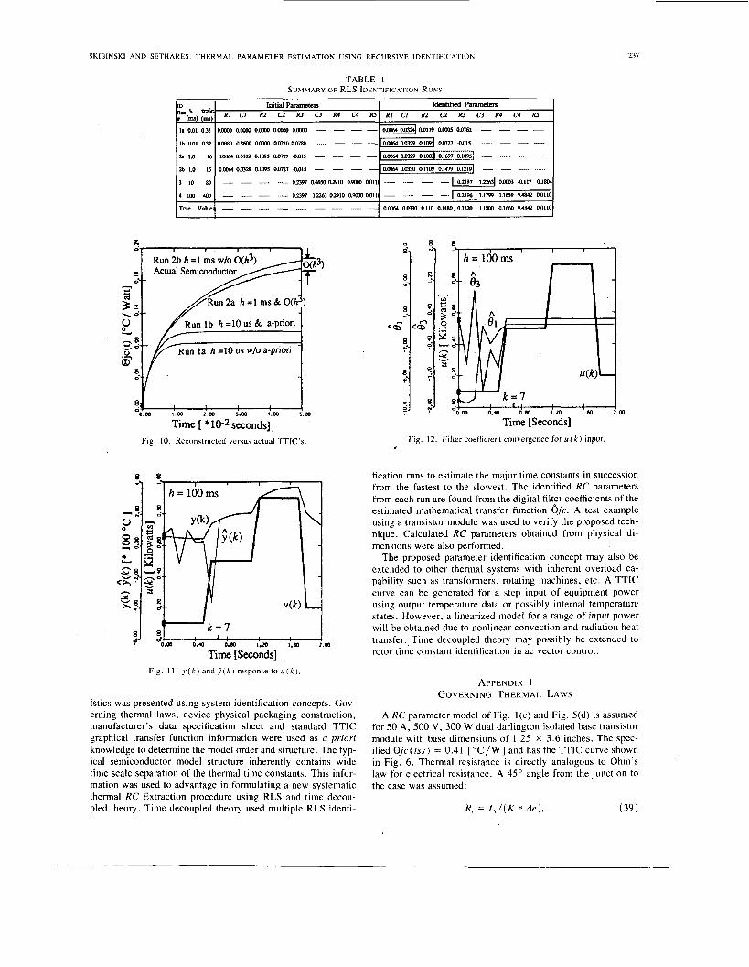
Test Case Results Table I1 results show that only four basic identification runs
were needed to identify the nine unknown RC parameters. Cor- rectly identified parameters in Table I1 are enclosed in a solid box. The four basic time constants listed in the T,,~‘ column are a direct result of the 8 parameter initialization procedure using (8e)-(8i) and the actual TTIC of Fig. 6. A suitable sampling rate for each ID run was derived from the T ~ , ~ ~ column by ap- plying (28).
The R1, R2, R3, C1 and C2 values were identified in 2 ID runs using the Fast 2nd order 6 j c model. Run la used the Sod- erstrom starting conditions assuming no a priori parameter in- formation. As seen from Table 11, R1 and C1 are properly identified, as expected, for h = 10 ps. Run lb shows that ad- ditionally R2 can be correctly identified by using all the a priori initial parameter estimates from Table I. Following the TDT procedure, the output identified parameters from run lb were used as initial parameter estimates for run 2 using h = 1 .O ms. Run 2a results show that the final R3 and C2 values enclosed by the dashed box in Table I1 are within 20% of the actual val- ues. This error is due to the method of calculating true y ( k ) using the linear difference equation rather than the TTIC ap- proach. This is caused by the dc gain discretization error intro- duced by the O ( h 7 ) term in the b2 filter coefficient of Appendix 11. Run 2b removed this error term resulting in final identified parameters within 0.1% accuracy. Fig. 10 shows a graphical comparison of ID runs la, lb, 2a, and 2b by reconstructing the TTIC from corresponding identified RC parameters.
CompoFents R3, R4, R5, C3 and C4 were identified using the slow e j c model in runs 3 and 4. The initial parameter esti- mate for R3 in run 3 was determined by adding the R1, R2, and R3 values identified from run 2b. The remaining initial param- eters were obtained from the 8 Initialization procedure and Ta- ble l . The results from run 3 show that, similar to run lb, the R3-C3 parameters associated with the faster time constant are correctly identified. Run 4 used these two component values along with estimates for R4, R5 and C4 from Table I as input parameters. The final identified parameters were within 0.2 % of the actual values. Figs. 11 and 12 show typical identification waveforms for run 4 with h = 100 ms.
Fig. 11 illustrates the output error equation, y ( k ) = y ( k ) - j ( k ) , being driven to zero in k = 7 samples. After time k = 7, the y ( k ) and j ( k ) temperature response waveforms to the U ( k ) sequence are identical. The u (k ) power sequence consists of six similar amplitude pulses before changing at k = 7 . Fig. 12 depicts the same u (k ) power sequence applied as inAFig. 11. In addition, a typical RLS convergence pattern for two 8 parameter values is shown. The digital filter coefficients, 8, = al and 8, = bo, are shown dynamically adapting to new values to satisfy the y ( k ) error equation and also reach steady state a t k = 7 samples. The steady state values of the five identified 0, were used to further extract the model RC parameters.
VIII. CONCLUSION This paper has identified a need for a device thermal model
to maximize simulation capability by solving both the electrical and thermal network models simultaneously. A new approach to the problem of determining device thermal model character-
SKIBINSKI AND SETHARES: THERMAL PARAMETER ESTIMATION USING RECURSIVE IDENTIFICATION
m Initial Parameters y&) E RI CI R2 C2 R3 C3 R4 C4 W
I. 0.01 0.32 0 . m 0 . m 0 . m 0 . m 0 . m - - - -
231
Idenrifed Panmeten RI CI R2 C2 R3 C3 R4 C4 RS
0 . m om 0.0179 0.m 0.0762 - - - -
TABLE I1 S U M M A R Y OF RLS IDENTIFICATION RUNS
Ib 0.01 0.32
1.0 16
zb 1.0 16
3 IO 80
4100 400
T* Valq
Om80 03600 ODDJ 0.UZZO 0,0780 - - - - 0.006) OD329 O.IO9i OD727 0.015 - - - - 0 . m o m s 0.1095 o m n 0.015 - -- - - 10.- 0 . m O.IOE&!.L~-~* - - - -- a m oms 0.10ss 0.0~27 0.015 - - - - 0 . m 011330 0.1109 0.1479 0.1219 - - - - -- - - 0.2397 066M 02.910 0 . W 0.0lll - - - - -1 0.m3 0.117 0.1804
-- - - -- 0,2397 12263 02910 0 . W 0,Ollf - - - - 0.23% 1.1799 1.1659 9.4842 0.011
- _- - ._ - - - 0 . m o.mM 0.110 0.1480 o.im 1.1880 0.1660 9 . ~ 2 0.0110
L
Time [ seconds], Fig. 10. Reconstructed versus actual TTIC's.
Time [Seconds] Fig. 1 1 . ? . ( k ) a n d 9 ( k ) r e s p o n s e t o u ( k ) .
istics was presented using system identification concepts. Gov- erning thermal laws, device physical packaging construction, manufacturer's data specification sheet and standard TTIC graphical transfer function information were used as a priori knowledge to determine the model order and structure. The typ- ical semiconductor model structure inherently contains wide time scale separation of the thermal time constants. This infor- mation was used to advantage in formulating a new systematic thermal RC Extraction procedure using RLS and time decou- pled theory. Time decoupled theory used multiple RLS identi-
-
om 0.0 0.m 1.m 1.60 z.m Time [Seconds]
Fig. 12. Filter coefficient convergence for u ( k ) input.
fication runs to estimate the major time constants in succession from the fastest to the slowest. The identified RC parameters from each run are found from the digital filtfr coefficients of the estimated mathematical transfer function ejc. A test example using a transistor module was used to verify the proposed tech- nique. Calculated RC parameters obtained from physical di- mensions were also performed.
The proposed parameter identification concept may also be extended to other thermal systems with inherent overload ca- pability such as transformers, rotating machines, etc. A TTIC curve can be generated for a step input of equipment power using output temperature data or possibly internal temperature states. However, a linearized model for a range of input power will be obtained due to nonlinear convection and radiation heat transfer., Time decoupled theory may possibly be extended to rotor time constant identification in ac vector control.
APPENDIX I GOVERNING THERMAL LAWS
A RC parameter model of Fig. I(c) and Fig. 5(d) is assumed for 50 A, 500 V, 300 W dual darlington isolated base transistor module with base dimensions of 1.25 X 3.6 inches. The spec- ified ejc(tss) = 0.41 [ "C/W] and has the TTIC curve shown in Fig. 6. Thermal resistance is directly analogous to Ohm's law for electrical resistance. A 45" angle from the junction to the case was assumed:
Rj = L , / ( K * A e ) , (39)

238 IEEE TRANSACTIONS ON POWER ELECTRONICS, VOL. 6. NO. 2, APRIL 1991
TABLE 111 CALCULATED PARAMETER SPREADSHEET
I Mnkrlrl I (mils) I (sq. inch) I (q. inch)
Sn-Pb 75-25 17 0.43 x 0.43 0.43 x 0.42
CU block/ 63 I 0.6 x 0.6 I 0.6 x 0.6 I 1 I
;z:g I 4 I 0.6x0.6 1 0.6x0.6
0.6 x 0.6 0.6 x 0.6
Cu base 1.2 X 1.2 0.75x0.75
= t - = t -
= t / 2 = I 1 2 -
(C/W 0.008 0.008
0.087
0.016 0.016
0.097 0.0089 0.0089
0.012
- - - - -
- - -
0.109
0.027
0.010
- - 0.010
TABLE IV MATERIAL PROPERTIES ASSUMED
Material K [ W / ( ” C - i n ) ] p [Ib/cu. in.] C,, [W-S/lb-”C]
The digital filter coefficients used in ( 1 8) transfer function are
a , = -2.0 + K2, + KZ2 + K32
a2 = 1.0 - K 2 , - K22 - Ks2 + K21 * K32
bo = R ,
bl = RI{ -2.0 + K l , i- K,, + K22 + K32 - 0.5 * K1, * K , , }
b2 = Rl(1.0 - K l , - K2l - K22 - K32 + 0.5 * K , , * K2i
+ ’ ’ . KII * K22 + K , , * K32 + K21 * K32 - O ( h s ) }
where the O ( h 3 ) = 2nd order error term = 0.5 * K , , * K 2 , * K 3 2 .
~
Silicon 2.134 0.083 303 280°C Solder
(Sn 10-Pb90) 0.914 -
Molydemum 3.296 0.369 1 I5 180°C Solder
(Sn75-Pb25) 0.914 - Ceramic 0.510 -
Copper 9.77 0.320 175
-
- -
ACKNOWLEDGMENT
The author’s wish to thank Wisconsin Alumni Research Foundation (WARF) and K . Phillips, J . VanderMeer of Eaton for project support, and Prof. D. Divan and S. Bhattacharya for helpful suggestions.
L, = thickness [inch] of material along heat flow path; K = material thermal conductivity from Table IV;
Ae = cross section area [ sq. in. ] perpendicular to heat flow
in calculating an effective heat spreader area { Ae } for succeed- ing layers with a much greater true cross sectional area { Ac }. Thermal resistance { R , } is calculated to the midpoint of each major heat capacity material where the capacitance { C, } is as- sumed a lumped parameter. However, the silicon chip is an ex- ception where it is assumed that the top 1/2 of the thickness { L, } is really the distributed power source { P } . The ceramic insulator (26% ) and solder interfaces ( 34% ) account for 50% of the specified e jc ( tss ).
The thermal capacitance is calculated using true material vol- ume:
path;
c, = p * c p * v, (40) p = density of the material from Table IV,
V = true material volume ( L , * A C ) [ in3 I . Cp = specific heat of the material from Table IV,
APPENDIX I1 DISCRETE TRANSFER FUNCTION MODEL
Let the following constants be defined for a chosen sample time h:
REFERENCES
[ I ] F. Gutzwiller and T. Sylvan, “Power semiconductor ratings un- der transient and intermittent loads,” in Rec. AIEE Winter Meet- ing, 1959.
[2] P. Hower, D. Blackburn, F. Ottinger, and S . Rubin, “Stable hot spots and second breakdown in power transistors,” in IEEE Power Electronics Specialist Conf. Rec., 1976.
[3] R. Chick, “How to power rate a transistor,” Solid State Power Conv., Mar./Apr. 1977.
[4] “Transistor safe operating area,” Amperex Report S169, 1981. [5] W. C. Schultz, “Power transistor safe operating area,” Power
Conversion Inrernational, July/Aug. 1982. (61 R. Prest and J . Van Wyk, “Improved dc modeling of high current
bipolar transistors for accurate converter simulation,” in IEEE IAS Annual Conf. Rec., 1989, p. 1235.
[7] S. Menhart and W. Portnoy, “Development of a secondary breakdown model for bipolar transistors,” in IEEE IAS Annual Conf: Rec., 1989, p. 1243.
[8] G. Skibinski, W. Sethares, and D. Divan, “Adaptive current reg- ulators to maximize overload capability,” Wempec notes.
[9] K. Astrom and P. Eykhoff, “System identification-A survey,’’ in 2nd IFAC Symp. Identification and Process Parameter Esti- mation Rec., 1970; also in Automatica, vol. 7, pp. 123-162, 1971.
[IO] I. Gustavson, “Survey of applications of identification in chem- ical and physical processes,” in 3rd IFAC Symp. Identification and System Parameter Estimation Rec., 1973.
[ 1 I] F. Ottinger, D. Blackburn, and S . Rabin, “Thermal character- ization of power transistors,” IEEE Trans. Electron Devices, vol.
[ 121 “Thermal resistance measurements of conduction cooled power transistors,” EIA Standard RS-313-13, 1975 Electronic Industry Association, 2001 Eye Street, N.W., Washington, DC 20006.
[I31 K. Astrom and Wittenmark, Computer Controlled Systems. En- glewood Cliffs, NJ: Prentice Hall, 1984.
[ 141 S. Wolfram, Mathemarica. Reading, MA: Addison-Wesley, 1988.
ED-23, 1976.

SKIBINSKI AND SETHARES: THERMAL PARAMETER ESTIMATION USING RECURSIVE IDENTIFICATION 239
C. Johnson, Lectures on Adaptive Parameter Estimation, Lecture 5 , “Persistant excitation and parameter convergence.” Engle- wood Cliffs, NJ: Prentice Hall, 1988. ACSL Ref Manual, Mitchell & Gauthier Assoc.. Concord, MA. B. D. 0. Anderson, R. R. Bitmead, C. R. Johnson, Jr., P. V. Kokotovic, R. L. Kosut, I. M. Y. Mareels, L. Praly, and B. D. Reidle, Stability of Adaptive Systems: Passivity and Averaging Analysis. S. Haykin, Adaptive Filter Theory. Englewood Cliffs, NJ: Pren- tice-Hall,
Cambridge, MA: MIT Press, 1986.
Gary L. Skibinski was born in West Allis, WI in 1953. He received the B.S.E.E. and M.S.E.E. degrees from the University of Wis- consin-Milwaukee in 1979 and 1980, respec- tively. He is currently a Ph.D. candidate at the University of Wisconsin-Madison.
He joined Eaton Corporation in 1976 as a Design Engineer in the Solid State Power Con- version Lab where he has worked on the design of a voltage source inverter propulsion drive for a Navy minisubmarine, a static rod drive sys-
tem for Navy nuclear reactors, and a commercial current source in- verter drive. He joined Allen Bradley Corporate R & D in 1980 as a
Project Engineer working on a real time data acquisition motor dyna- mometer laboratory. From 1982 to 1985 worked as Senior Project En- gineer on design and analysis of dc and ac servo controllers. In 1985 he was appointed Principal Engineer at RTE Corporation R & D work- ing on UPS and switching supply topologies. His present interest is investigating new power electronic converter technologies.
Mr. Skibinski is a member of Phi Kappa Phi and Tau Beta Pi. He is a Professional Engineer in the State of Wisconsin and the recepient of two Prize Paper awards at the 1987 and 1990 IEEE IAS Annual Con- ferences
William A. Sethares (S’84-M’S6-S’SS-M’87) received the B.A. degree in mathematics from Brandeis University, Ithaca, NY.
He has worked at the Raytheon Company as a Systems Engineer and is currently with the Department of Electrical and Computer Engi- neering at the University of Wisconsin in Mad- ison. His research interests include adaptive systems, and applications of system identifi- cation techniques to control, power, and semi- conductor processes.