the engineering, design, and fabrication facility: a … hopkins apl technical digest, volume 21,...
TRANSCRIPT
H. K. CHARLES, JR., AND J. A. WEINER
478 JOHNS HOPKINS APL TECHNICAL DIGEST, VOLUME 21, NUMBER 4 (2000)
T
The Engineering, Design, and Fabrication Facility:A Unique APL Resource
Harry K. Charles, Jr., and Joel A. Weiner
he Engineering, Design, and Fabrication (EDF) Facility is a unique resourceproviding a wide range of development, engineering, design, fabrication, and testingservices for APL and its external customers. The facility consists of modern laboratoriesand specialized equipment and processes. It is staffed by skilled engineers, scientists,technicians, and craftspeople, all dedicated to the production of high-quality electronic,electromechanical, and mechanical hardware. The EDF is a flexible, dynamic resourcethat responds rapidly to customer needs in both traditional and new business arenas.With its technology and personnel, the EDF is poised to deliver advanced services andhardware for many years to come. (Keywords: Electronic services, Engineering design,Fabrication, Hardware, Mechanical and material services, Prototyping.)
INTRODUCTIONThe Engineering, Design, and Fabrication Facility
(EDF) of the Technical Services Department (TSD) isan integrated Laboratory resource for the development,design, fabrication, testing, and qualification of proto-type, one-of-a-kind, and limited-quantity advancedelectronic, electromechanical, and mechanical hard-ware. The facility consists of extensive equipment andlaboratory resources, coupled with the expertise ofskilled scientists, engineers, technicians, and craftspeo-ple. It also maintains almost 200 standard processes andprocedures that capture detailed design and fabricationknowledge to facilitate project documentation andtechnology transfer. These resources reside primarily inTSD’s Electronic Services Group (TSE) and Mechan-ical Services Group (TSM); additional support comes
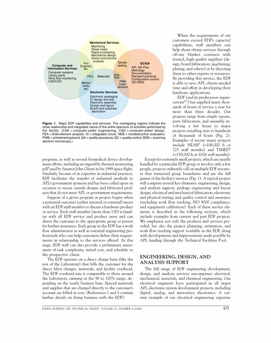
from the Department’s computer and information sys-tems services (especially computer-aided engineering)and fiscal administration. The groups are functionallyaligned, with a minimum of overlap and service dupli-cation. Figure 1 illustrates the major facility capabilitiesand service functions. Further details of EDF servicescan be found in articles by Hider et al. and Wilson etal., this issue, and Ref. 1.
By charter, EDF staff maintain a working knowledgeof modern engineering, design, fabrication, and testingmethods to serve as the Laboratory’s principal resourcefor manufactured hardware. This expertise is a key ele-ment in APL’s ability to transfer technical hardwareknowledge to industrial partners. Particularly notablesuccesses in this area have been the Transit2 and Aegis3
JOHNS HOPKINS APL TECHNICAL DIGEST, VOLUME 21, NUMBER 4 (2000) 479
THE ENGINEERING, DESIGN, AND FABRICATION FACILITY
programs, as well as several biomedical device develop-ment efforts, including an ingestible thermal monitoringpill4 used by Senator John Glenn in his 1998 space flight.Similarly, because of its expertise in industrial practices,EDF facilitates the transfer of industrial methods toAPL’s government sponsors and has been called upon onoccasion to rescue outside designs and fabricated prod-ucts that do not meet APL or government requirements.
Support of a given program or project begins whena potential customer (either internal or external) meetswith an EDF staff member to discuss a hardware productor service. Each staff member (more than 130) is famil-iar with all EDF service and product areas and candirect the customer to the appropriate group or personfor further assistance. Each group in the EDF has a workflow administrator as well as essential engineering pro-fessionals who can help customers define their require-ments in relationship to the services offered. At thisstage, EDF staff can also provide a preliminary assess-ment of task complexity, initial cost, and schedule tothe prospective client.
The EDF operates on a direct charge basis (like therest of the Laboratory) that bills the customer for thedirect labor charges, materials, and facility overhead.The EDF overhead rate is comparable to those aroundthe Laboratory, running in the 90 to 100% range, de-pending on the yearly business base. Special materialsand supplies that are charged directly to the customer’saccount are billed at cost. (References 1 and 5 containfurther details on doing business with the EDF.)
When the requirements of ourcustomers exceed EDF’s capacity/capabilities, staff members canhelp them obtain services throughoff-site blanket contracts withtrusted, high-quality suppliers (de-sign, board fabrication, machining,plating, and others) or by directingthem to other experts or resources.By providing this service, the EDFis able to save APL clients neededtime and effort in developing theirhardware applications.
EDF (and its predecessor organi-zations6,7) has supplied many thou-sands of hours of service a year formore than three decades. Ourprojects range from simple repairs,parts fabrication, and assembly in-volving a few hours to majorprojects entailing tens to hundredsof thousands of hours (Fig. 2).Examples of recent major projectsinclude NEAR8 (≈106,000 h or725 staff months) and TIMED9
(≈150,000 h or 1026 staff months).Except for extremely small projects, which are usually
handled by a particular EDF group or involve only a fewpeople, projects ordinarily call on multiple EDF resourc-es that transcend group boundaries and use the fullgamut of the facility’s services (Fig. 1). A typical projectwill comprise several key elements: engineering, design,and analysis support; package engineering and layoutdesign; electrical and mechanical fabrication; electronicand physical testing; and quality control and assurance(including work flow tracking, ISO 9000 compliance,and equipment calibration). Each of these service ele-ments is described in the following sections, whichinclude examples from current and past EDF projects.We emphasize not only the products and services pro-vided, but also the project planning, estimation, andwork flow tracking support available in the EDF, alongwith developments and improvements made possible byAPL funding through the Technical Facilities Pool.
ENGINEERING, DESIGN, ANDANALYSIS SUPPORT
The full range of EDF engineering development,design, and analysis services encompasses electrical,mechanical, materials, and chemical engineering. Ourelectrical engineers have participated in all majorAPL electronic system development projects, includingdigital, analog, and microwave electronics. A cur-rent example of our electrical engineering expertise
Mechanical ServicesMachiningSheet metalRapid prototypingMechanical designStress and thermal analysis
FEA
Pro/Engineer,
etc.
Materials
Mentortools,etc.
Tensiletesting
SEM,NDE
PWBcross-
sections
QC/QAAPL QA PlanMetrologyDocumentationStandard practicesConfiguration controlISO 9000
Electronic ServicesElectronic packagingIC design and testElectronic assemblyDesign and layoutBoard and substrate fabrication
Computer systemsLibrary partsWork flow monitoringCAE/CAD
Computer andInformation Services
Figure 1. Major EDF capabilities and services. The overlapping regions indicate theclose relationship and integrated nature of the entire spectrum of activities performed bythe facility. (CAE = computer-aided engineering, CAD = computer-aided design,FEA = finite-element analysis, IC = integrated circuit, NDE = nondestructive evaluation,PWB = printed wiring board, QA = quality assurance, QC = quality control, SEM = scanningelectron microscopy.)

H. K. CHARLES, JR., AND J. A. WEINER
480 JOHNS HOPKINS APL TECHNICAL DIGEST, VOLUME 21, NUMBER 4 (2000)
(Fig. 3) is the Digital Multibeam Steering (DIMUS)chip, a custom-designed integrated circuit (IC) for adigital multibeam sonar beamformer (steering ele-ment).10 This chip contains approximately 2 milliontransistors and is about 3.5 cm2. A DIMUS chip, whenintegrated with nine others on a single printed wiringboard (PWB), replaces an entire floor-standing rack ofelectronic equipment in APL’s Trident Sonar ProcessorAnalyzer (TSPAN) System.11
Figure 4 illustrates our thin film multilayer technol-ogy. This high-density substrate technology uses a sil-icon carrier coated with multiple layers of copper met-allization (with chromium adhesion layers) andpolyimide interlayer dielectrics. The technology is ca-pable of trace densities12 approaching 200 cm/cm2. Atthese densities approximately 1 mile of circuit trackcould be placed in a 25 � 25 cm space. Thin film
multilayer technology has beenused to package some of the dens-est APL-produced circuitry todate. The role of such dense, highchip count modules, called multi-chip modules (MCMs),13 is ex-pected to increase.
Building MCMs, because oftheir large population of denselyplaced chips, requires a great em-phasis on chip reliability to ensuremodule yield. Figure 5 presents theyield of an MCM containing twodifferent chip types (Type 1 andType 2) as a function of the knowngood die (KGD) probabilities.14
Here, module total cost is comparedfor the “no repair” case and a “singlerepair” with increasing complexity.It is clear from the sequence shownthat repair capability is key to im-proving the yield and lowering thecost of high-density MCMs. TheEDF has developed several repairmethodologies for its MCM tech-nology. Besides these thin film de-posited MCMs (MCM-D), others,e.g., MCM-Cs (ceramic-based) andMCM-Ls (laminate-based), havebeen described elsewhere.15
In addition to the ingestible pill4
noted earlier, our engineers havesupported several other APL bio-medical initiatives, including aninfrared sensing system for the blind(IRIIS16), a virtual reality goggleprojection system for the JohnsHopkins Medical Institution andHonda Motor Company, advanced
three-dimensional bone modeling to study osteoporosisand injury, intravascular magnetic resonance imagingcoils,17 and a dual-energy X-ray densitometer18 to mea-sure bone and muscle loss in space. For these efforts,EDF personnel have performed a full range of engineer-ing development and design services along with fabri-cation and system evaluation. Other EDF engineeringactivities have provided design and analysis for ad-vanced APL projects such as the Cryogenic CrossbarSwitch,19 chip-on-board (COB) packaging,20 the palm-sized Command and Data Handling System,20 etc.
Electrical simulation models and thermal (temper-ature) and associated thermomechanical (stress/strain)models are fundamental to the development of ad-vanced electronic and mechanical systems for space,underwater, and biomedical applications. A typicalelectrical simulation model (SPICE Equivalent) and its
Figure 2. Distribution of customer-supported work for FY99 in the EDF. (a) Percentageof projects by department. (b) Percentage of projects by dollar value. (Note that almost 75%of EDF’s projects are at the $25,000 level or less.) (c) Percentage of dollar expendituresby department. (APL department designations: ADSD = Air Defense Systems,BISD = Business and Information Services, CLO = Director’s Office, HRSD = HumanResources and Services, PPSD = Power Projection Systems, RTDC = Research andTechnology Development, SD = Space, SSD = Strategic Systems, STD = SubmarineTechnology, TSD = Technical Services.)
RTDC8.9%
Other(BISD/HRSD/CLO)
15.9%
SD20.1%
ADSD9.8%
TSD24.3%
STD10.3%
SSD6.5%
PPSD4.2%
TSD14%
ADSD24%
Other8%
PPSD2%RTDC
3%
SD37%
STD6%SSD
6%
0.5%(>$1M)
0.9%(>$500K to
≤$1M)
38.8%(≤$5K)
36.0%(>$5K to ≤$25K)
15.9%(≥$25K to ≤$100K)
7.9%(>$100K to
≤$500K)
(a) (b)
(c)

JOHNS HOPKINS APL TECHNICAL DIGEST, VOLUME 21, NUMBER 4 (2000) 481
THE ENGINEERING, DESIGN, AND FABRICATION FACILITY
Figure 3. DIMUS IC chip custom-designed in the EDF. DIMUSuses CMOS technology and was designed with APL’s MAGIC,IRSIM, and ModelSim software and fabricated through theMOSIS network. It contains 2 million transistors and uses 0.8-�mdesign rules.
Figure 4. Thin film multilayer MCM. The substrate was fabri-cated using EDF’s copper/polyimide MCM-D technology. It isabout 13 cm2 and contains three buried layers of circuitry. Theassembled unit has 16 chips and over 1200 wirebonds.
Figure 5. MCM cost as a function of known good die (KGD) for a dual-chip population under conditions of no repair (a) and single repairof low (b), medium (c), and high (d) complexity.
Ring randomaccess
memory
Ringcomputation
section
Decouplingcapacitors
121 lead pingrid array package
30
15
0
Tota
l cos
t ($K
)
30
15
0
Tota
l cos
t ($K
)
30
15
0
Tota
l cos
t ($K
)
30
15
0
Tota
l cos
t ($K
)
0.9
0.9
1.0
KGD probability Type 1 KGD probability Type 2
0.9 1.0
KGD probability Type 1 KGD probability Type 2
0.9 1.0
KGD probability Type 1 KGD probability Type 2
0.9 1.0
KGD probability Type 1 KGD probability Type 2
(a) (b)
(d)
1.0
1.0 0.9 1.0 0.9
1.0 0.9
(c)

H. K. CHARLES, JR., AND J. A. WEINER
482 JOHNS HOPKINS APL TECHNICAL DIGEST, VOLUME 21, NUMBER 4 (2000)
results are shown in Fig. 6. Figure 7 shows thermalcontours and vibration amplitude for the Global Posi-tioning System (GPS) Full Signal Translator Modulecircuit board due to temperature increases of the indi-vidual components. The EDF’s thermal stress analysiscapability has furnished design and fabrication guide-lines for a wide range of electronic, electromechanical,and mechanical hardware. Figure 8 presents the resultsof a finite-element analysis performed on a TIMEDspacecraft packaging component.
PACKAGE ENGINEERING ANDLAYOUT DESIGN
The EDF has a long history of providing innova-tive package design and detailed layout support for avariety of APL programs. Our packaging engineersand layout designers use modern, advanced engineer-ing workstations coupled with specialized softwaretools to yield the drawings and electronic files nec-essary to drive automated manufacturing equipment
0
–20
–40
–60
Mag
nitu
de (
dB)
0 4 8 12 16 20
Frequency (GHz)
Transmitted power (S11)
Reflected power (S21)
1.2
1.0
0.8
0.6
0.4
0.2
0
Sig
nal a
mpl
itude
(V
)
50 100 150 200 250 300 350 400Time (ps)
Incident + reflected
Transmitted
0
–10
–20
–30
–40
–50
–60
Mag
nitu
de (
dB)
0 4 8 12 16 20Frequency (GHz)
Near-end noise (S23)
Far-end noise (S53)
0.040
0.020
0.030
0.010
0
Noi
se a
mpl
itude
(V
) Near-end noise
Far-end noise
100 150 200 250 300 350 400Time (ps)
1
23
45
6
25
50
25
125
(a)
(b) (c)
(d) (e)
Figure 6. High-speed stripline cables to MCM-soldered interconnection. (a) Physical layout (dimensions in mils; ports labeled 1 to 6).(b) S-parameter data for cable to MCM-soldered interconnection. (c) Signal transmission/reflection analysis (9% reflected noise).(d) Cross-talk analysis S-parameter data for coupled three-line model for cable to MCM-soldered interconnection. (e) Cross-talk noiseanalysis (3.7% near-end noise, <1% far-end noise).

JOHNS HOPKINS APL TECHNICAL DIGEST, VOLUME 21, NUMBER 4 (2000) 483
THE ENGINEERING, DESIGN, AND FABRICATION FACILITY
(photoplotters, board testers, numerically controlledmachine tools, etc.).
The EDF provides APL electrical engineers with adiverse set of design automation tools for use withCOB, MCMs, application-specific ICs (ASICs), field-programmable gate arrays (FPGAs), and PWBs. Mostof these tools are supplied by Mentor Graphics and cansupport both traditional schematic capture and themore recent hardware descriptive language (HDL)approach to design creation. The schematic entrymethod still accounts for almost 100% of the PWBdesign work, although APL engineers have begun toembrace HDL for their FPGA and ASIC designs.
An important aspect of any computer-aided design isthe ability to simulate the functionality and timing ofa design before building the hardware. We performed theservice, for each of the circuit application types men-tioned, with Mentor Graphics Software tools (AccuSim,QuickSim, ModelSim, H-Spice, and Continuum).These tools not only provide specific simulators forhomogeneous applications (e.g., all analog, all digital,etc.), but can also be combined on a single design usingthe Continuum Back Plane Mixed Signal Simulationkernel, thereby simultaneously simulating a mixed an-alog, digital, and HDL design.
Key to the effective use of design automation toolsat APL is a standardized parts library. The EDF now has
over 10,000 parts in its Mentor library. Each part de-fined in the library contains our in-house design rulesfor fabrication and assembly, and includes a schematicsymbol and board geometry. The library covers a widevariety of part types, including specific ASIC libraryelements that can be directly linked to the MOSISfoundries through Mentor’s Higher Education Program.As circuit designs embrace the latest in IC technology,the EDF will continue to maintain the library and buildnew library parts as an important service to the Lab-oratory’s engineering community.
Access to the library is gained through a simplemenu structure. The library is divided by circuit func-tion, i.e., resistors are in the resistor menu, ICs in theIC menu, etc. In addition, the EDF provides simulationmodels for many of the library parts. Through an annualsubscription contract, we can access (in addition to ourown models) over 13,000 digital simulation models. Wealso make a Mentor Graphics analog simulation libraryavailable for customer use.
Recently, the EDF has acquired a microelectrome-chanical systems (MEMS)21 software package devel-oped by Mentor Graphics. This allows direct support
(a)
(b)
96.1393.5590.9788.3958.8183.2380.6578.0775.4972.9070.3267.7465.1662.5860.00
Temperature (°C)
Figure 7. Analysis of the GPS Full Signal TranslatorModule chassis. (a) Constant temperature (isothermal) contours.(b) Dominant vibrational mode.
Figure 8. Finite-element analysis of a Minitek surface-mountconnector used on the TIMED spacecraft. (a) One-half symmetryfinite-element model of a single Minitek surface-mount receptaclecontact. (b) Von Mises stress contours for the Minitek connector.
Direction ofapplied load
Connectorreceptacle
contact
Solder joint
Printedcircuitboard
F = 20 grams-force
One-half symmetrymodel ofsurface-mountedconnector receptaclecontact
Maximum Von Mises stressin solder joint (≈7 MPa)
Von Mises stress(MPa)
(a)
(b)
2.82.62.42.22.01.81.61.41.21.00.80.60.40.20.0

H. K. CHARLES, JR., AND J. A. WEINER
484 JOHNS HOPKINS APL TECHNICAL DIGEST, VOLUME 21, NUMBER 4 (2000)
of the Laboratory’s MEMS efforts and provides asmooth interface with the Defense Advanced ResearchProjects Agency–subsidized MEMS foundry at theMicroelectronics Center of North Carolina. The pack-age includes a component library consisting of simula-tion models and layout generators for inertial sensors,actuators, optical devices, radio-frequency devices (RF-MEMS), display devices, and test structures.
The EDF maintains an on-site environmentally con-trolled Class A Halon-protected drawing vault thatcontains tens of thousands of engineering drawingsdating back to the 1970s. In addition to paper drawings,we have tape archives, i.e., CAE system backups andaperture cards (microfilm-like copies of each drawing),for each design. Hand-drawn and/or written forms suchas drawing change notices are scanned and added to thearchives along with the drawings they reference.
Since 1994, we have accomplished the online archi-val storage (and retrieval) of design information anddatabases using a product data management (PDM)tool. The PDM product currently being used isMetaphase by SDRC. It contains data for over 11,000drawings and over 1700 drawing change notices andengineering change requests. The data are available byaccessing a CD-ROM jukebox that now holds 34 CDswith over 13 GB of data. The PDM has been configuredto facilitate the drawing sign-off/approval for all draw-ing configuration levels (1, 2a, 2, and 3). The PDMproduct resides on an HP UNIX server and has anOracle database engine. Over 40 users (mostly engi-neers and designers) routinely access the PDM eitherdirectly from a UNIX workstation or from a PC runningan X-server package. PDM users can acquire report datavia an APL internal Web browser. Drawings and othergraphical attachments are in HDGL or TIFF format andcan be viewed with a readily available plug-in.
The EDF has a documented system for the rapidprototyping of PWBs. Depending on design complexity,as determined by component density and number ofboard layers, different software tools are used in therapid prototyping process. Pantheon Intercept softwareis used to create parts and perform the layout androuting of simple-to-medium complexity designs. Men-tor tools are used for more complex designs. A well-defined path through design, fabrication, and assemblyhas been established to provide contingencies for delaysat any step. The process has been employed successfullyon several Level 1 designs. Typical turnaround timeshave been on the order of 1 week.
On the mechanical side, the major piece of designsoftware is Pro/Engineer developed by Parametric Tech-nologies, Inc. Pro/E, as it is commonly called, is aninteractive tool based on parametric design methods.For example, instead of indicating the dimensions of abox as 10 cm in length (l), 5 cm in width (w), and 150cm in height (h), the box dimensions are described as
an analytic expression (e.g., lwh). The expression canbe composed of independent variables (such as l, w, orh), or one or more of the variables can be dependenton other variables being used to define the measure-ments of other objects in the design (e.g., the boxlength is equal to twice its width). This parametricapproach results in an increased emphasis on the cre-ation of a model of the design rather than a drawingof the design. The drawings are then simply the outputproducts of the model. Until the model or parametricrelationships are changed, the model remains invariantunder scaling. Thus, a change in an input (indepen-dent) dimension will change the output drawings toreflect the dimensional change, but the model willremain the same.
Pro/E can check for interference and can also calcu-late the weight (based on the density of the constituentmaterials) and center of gravity of the set of objectscomprising a design. A clipping feature allows a modelto be cross-sectioned at any depth, which enables theengineer or designer to better understand the relation-ships of objects within the design. In addition to draw-ings, Pro/E is capable of outputing databases that can beused directly by EDF’s numerically controlled machinetools. This allows for the unattended fabrication ofintricate mechanical parts, composite-resin rapid proto-types, and complex sheet metal assemblies.
ELECTRICAL AND MECHANICALFABRICATION
EDF’s electrical and electronic fabrication facilitiesare located in Building 13 (the Steven Muller Centerfor Advanced Technology). They include our certifiedPWB fabrication line (certified to MIL-PRF-55110Fand MIL-P-50884, Type 3 (GI Material) and Type 4(adhesiveless)) and Class 1,000 clean rooms22 used tofabricate and assemble microelectronic devices andmodules such as the large, multilayer, high-densityPWB produced for the TRIAGE Program shown inFig. 9. The MCM substrate shown in Fig. 4 is a recentexample of our microelectronic activity.
Recent EDF work on fine-line boards with blind andstaggered vias for COB applications20 is illustrated inFig. 10. COB can potentially miniaturize APL systemsby a factor of 10 to 100. Examples of a COB implemen-tation of a standard spacecraft electronics box areshown in Fig. 11. Essential to making the COB processwork was EDF’s development of a neutral pH autocat-alytic gold plating solution, along with associated pro-cessing methods.23
Other advanced board development efforts have in-volved the use of electro-optic–sensitive polymers suchas the dielectric layers in MCMs. These layers can beprobed nondestructively using a laser. Laser mapping ofthe electric fields within the dielectric layers adjacent to

JOHNS HOPKINS APL TECHNICAL DIGEST, VOLUME 21, NUMBER 4 (2000) 485
THE ENGINEERING, DESIGN, AND FABRICATION FACILITY
device structures of interest can be made. This APLinvention offers great promise for testing complex elec-tronic structures.24 The polymer material is made electro-optic by doping and selective poling (application of astrong electric field while material iscured). Thus, regions of doped andunpoled material can be made adja-cent to doped and poled material. Asthere is an index change in thedoped material upon poling, integrallight guides can be made selectivelyin the dielectric layers. These APL-developed techniques,25 therefore,offer the potential for integral lightguides in MCM dielectrics alongwith the ability to nondestructivelyevaluate module performance.
In addition to advanced-per-formance circuits and boards forhigh-reliability spaceflight use, EDF’selectronic fabrication facilities cre-ate a large volume of more conven-tional electronics. These are in-tended for ground and shipboard
Figure 9. High-density PWB developed for the TRIAGE Pro-gram. This radar data collection board contains 10 circuit layers,4883 vias, and 422 components, with 6052 internal componentconnections and 624 input/output pins. This single board replacedthe five boards used in a previous system.
Figure 10. COB substrate containing blind and staggered vias.This 12.3 � 12.3 cm board is being used for the palm-sizedCommand and Data Handling System.19
Figure 11. COB implementation of the NEAR Command/Telemetry Processor (24 � 24� 17 cm, 5 kg) compared with the palm-sized Command and Data Handling System (11� 11 � 5 cm, 0.5 kg).
use and support myriad one-of-a-kind experiments con-ducted by our scientists and engineers, both at the Lab-oratory and off-site.
Mechanical fabrication is performed with advancedmachine tool equipment located in Buildings 14, 39,and 41. This equipment includes computer-numerical-ly-controlled (CNC) lathes, mills, turning centers, andsheet metal punches. Three CNC electrical dischargemachine tools, plus both carbon dioxide26 and Nd:YAGlasers (in Bldg. 13), are the heart of EDF’s advancedcontactless machining activity.

H. K. CHARLES, JR., AND J. A. WEINER
486 JOHNS HOPKINS APL TECHNICAL DIGEST, VOLUME 21, NUMBER 4 (2000)
A computer-controlled rapid prototype machine isalso available. It is capable of making realistic (dimen-sionally accurate) three-dimensional polymer replicasfrom files downloaded from our CAE systems. Examplesof rapid prototype–produced replicas are shown in Fig.12. EDF’s organic composite fabrication activities arehoused in Building 14. Further description of our com-posite work is given by Wilson et al., this issue.
Fabrication involves more than just the manufactureof advanced electrical and mechanical parts and systems.It also involves the application of the tools normallyassociated with hardware fabrication to support otheraspects of APL’s scientific and engineering activities. Forexample, EDF’s photolithographic resources have beenused to pattern gratings for optical experiments, sensorsfor biomedical and ocean physics applications, and thinfilms for basic research. Our carbon dioxide laser ma-chine tool26 has been employed in material ablationstudies and for novel pattern generation in unconven-tional materials. It has also served as a heat source formaterial alloying. The rapid prototyping system has beenused to fabricate real parts (not just models or replicas)in short-duration experimental situations. Such innova-tive use of standard production tools, necessary for APL’sand EDF’s mainstream hardware production, gives APLa flexible resource to augment its research facilities inother parts of the Laboratory.
Our expertise in the fabrication of hardware is achief element that distinguishes the Laboratory frommany other research and development centers. This
hands-on hardware development resource of the EDFhelps form APL’s internationally known systems engi-neering capability.
ELECTRONIC AND PHYSICALEVALUATION
The EDF offers a wide range of electronic and phys-ical testing services. Our electronic test equipment canperform exacting electrical tests for analog, digital, andmicrowave circuits. Components and circuits can betested from DC to 50 GHz. This allows us to verifymanufacturers’ published data sheets, provide deviceand subsystem data not available from manufacturers,and evaluate “edge-of-the-envelope” parameters whencommercial-grade parts are pushed beyond their pub-lished limits. Tools and expertise in the EDF enable usto execute extensive DC parametric tests on devices.For example, leakage current values can be validatedor the variation of leakage current with respect tosupply voltage can be measured. In addition, transistorcharacteristic curves can be generated for all devicetypes (bipolars, field-effect transistors, power transis-tors, hetero junction bipolar transistors, etc.).
We can also perform AC characterization of com-ponents of frequencies from a few millihertz to 50 GHzusing vector network analyzers. Spectral analysis capa-bility up to 26.5 GHz is currently available, with plansto upgrade to 50 GHz. These measurements are used tocharacterize passive and active circuit components,
subsystems, and materials for fre-quency, time, phase, and noise pa-rameters. The EDF specializes inthe design and fabrication of cus-tom test fixtures and the use of au-tomated testing equipment andmethods to greatly speed the test-ing process and eliminate operatorbiases and errors. Over the last fewyears, these methods have beenused on a variety of APL programs,including CASSINI, MSX, NEAR,ACE, and TIMED.
Virtually every electronic de-vice—whether a printed circuit as-sembly, an MCM, or a custom IC—involves a substrate onto which oneor more components are attached.This substrate contains conductivetraces that interconnect the deviceto other circuit elements on theboard as well as interface it withpower supplies and adjacent mod-ules in the system. Depending onthe application and design, the sub-strate will take many forms. It may
(a)
(b)
(c)
(d)
(e)
(f)
(g)(h) (h)
(i)
(j)
(l)
(m)
(k)
Figure 12. Rapid prototype replicas produced by an EDF automated polymer castingmachine. (a) TIMED Doppler Interferometer telescope mount. (b) Model of 443 Erosasteroid. (c) Impeller thruster. (d) Speaker-mount for Primate Vocalization Program. (e)Planetary gear. (f) Clamp for Primate Vocalization Program. (g) Gridded array. (h)Transmitter boxes for Primate Vocalization Program. (i) SCAMP pod faring. (j) Videodisplay chip mount/virtual reality helmet. (k) TIMED solar array bracket. (l) Mach 6supersonic nozzle for dual-combustor ramjet. (m) Impeller.
JOHNS HOPKINS APL TECHNICAL DIGEST, VOLUME 21, NUMBER 4 (2000) 487
THE ENGINEERING, DESIGN, AND FABRICATION FACILITY
be a multilayer printed circuit assembly with internaltraces and interconnecting vias of plated copper, a1-�m-thick thin film of aluminum or gold on a sili-con wafer, silk-screened patterns of conductive tracesand resistors on a ceramic substrate, or many otheralternatives.
With today’s demand for smaller devices, higherfrequencies, and tighter specifications, many of thefabrication techniques used to create the circuit ele-ments on the substrate are being pushed to their limits.The substrate must therefore be tested to ensure thatconductors are not inadvertently shorted to each otherand are continuous between the elements being con-nected. Elimination of the patterned substrate as apotential cause of failure saves time and money, asexpensive parts are not assembled onto a substrate thatis found to have incorrect or defective circuitry.
The BSL LinearProbe II Tester in the EDF has beenemployed for the past 5 years to perform 100% testingof all substrates used in the assembly of electronic devic-es. This fixtureless flying probe system is designed to testeither bare or populated substrates. In 1998, over 800printed circuit boards and other substrates were tested.The system simultaneously tests both sides of a substrateup to about 61 � 61 cm, regardless of the material ofconstruction. The average double-sided printed circuitboard takes less than an hour to test, including initialmachine setup and CAE file compilation.
The tester evaluates all circuitry networks (“nets”)for opens and shorts. Testing for opens is accomplishedusing a standard four-wire resistance measurement.Testing for shorts uses a capacitance measurement fortest node reduction, and then resistance for verificationof the suspect shorts; another option is to comparemeasured net resistance to a predetermined standard.The tester can be configured with a variety of probetypes (size and alloy) depending on the pad size andmaterial. Probes as small as 45 �m in diameter areavailable, permitting contacting to pads as small as 90�m in width. Probe location is repeatable to ±5 �m.Depending on which probes are used, up to 20 tests persecond can be performed.
The BSL tester can interpret a variety of CAE da-tabase formats to determine where to probe each net.The CAE file supplies the necessary location, nomen-clature, and net information to the tester. If no databaseis available, the tester can be manually “taught” wherethe testing points are located. In either case, it cansequentially test up to four identical substrates on acommon panel. The tester can also be used to test fornet-to-net isolation breakdown by applying a highvoltage between adjacent traces and monitoring forcurrent flow.
In addition to electronic equipment, the EDF main-tains and operates a complete range of physical testand failure analysis equipment to support our internal
hardware fabrication and to provide physical testingservices to our customers. Physical testing includesmechanical stress/strain, hardness, and metallurgicalmicrostructural analysis along with a suite of nonde-structive evaluation tools (e.g., several methods of ul-trasound evaluation, acoustic microscopy, and eddycurrent testing).
A full array of advanced material and chemicalevaluation tools also exists within the EDF. Such toolsas a scanning electron microscope, energy dispersive X-ray analyzer, Fourier transform infrared spectrometer,inductively coupled plasma spectrograph, and tabletopsecondary ion mass spectrometer are routinely used insupport of efforts for TSD, Laboratory programs, andsponsors. For example, in the Standard Missile Pro-gram, the protective nickel plating on the copper caseof a high-power electronic switch was found to bepeeling from a large percentage of devices. Since themissile manufacturer had only one vendor for thisspecialized device, missile production was threatened.Because of its varied imaging capabilities and detectors,the scanning electron microscope proved to be an idealtool for diagnosing the problem. Upon optical micro-scope inspection, the copper exposed by the peeling didnot appear to differ greatly from surfaces in which thenickel layers had been poorly adhered to the copperduring the plating operation. However, energy disper-sive X-ray (Fig. 13a) and Robinson backscattered elec-tron imaging (Fig. 13b) analysis of the blistered areashowed silver beneath the nickel.
An investigation of the processes used to fabricatethe device indicated that the package had electricalfeed-throughs brazed to the copper case before plating.The presence and distribution of the silver showed thatthe copper/silver brazing alloy had wicked along smallgrooves that were introduced into the surface during themachining of the case. The chemical baths used to cleanthe packages prior to nickel plating had been selectedwith the assumption that the surfaces were only copper,with no silver present. The silver left on the surface fromthe brazing operation had reacted with the ambient airto form compounds that were not removed during thecleaning process. Thus, a thin layer of contaminant waspresent during the nickel plating process, and the de-posited nickel could not atomically bond to the coppersurface. With this input, the vendor was able to improvehis process and deliver acceptable parts.
QUALITY CONTROL ANDASSURANCE
InspectionThe EDF maintains a fully staffed and equipped
quality assurance capability. Our materials analysisand quality assurance facilities offer customers many

H. K. CHARLES, JR., AND J. A. WEINER
488 JOHNS HOPKINS APL TECHNICAL DIGEST, VOLUME 21, NUMBER 4 (2000)
Ag L Ni K
Cu K BLST1 BOTTOM FK
(a)
(b)
Figure 13. Energy-dispersive X-ray spectrum (a) and dot maps(b) of a blister on the nickel-coated copper case of a high-poweredelectronic switch. Dot maps shown are for silver, nickel, copper,and a scanning electron micrograph of the region.
inspection, configuration control, documentation con-trol, storage, and parts kitting (preparation of assemblykits) operations. These services are central to our abilityto ensure that our customers’ quality assurance require-ments are met. Major documents controlling EDF ac-tivities in this area—the Laboratory’s Quality AssurancePlan,27 Hardware Configuration Management Manual,5
Electromechanical Hardware Workmanship StandardsManual,28 and nearly 200 standard processes and pro-cedures29—set standards and directions for our opera-tions. As part of EDF’s quality assurance practice, staffare trained and certified in many skill areas. For exam-ple, the EDF operates and maintains a fully certifiedNASA solderer training program.30 Every 2 years, ap-proximately 30 Laboratory employees are certified tosolder or inspect to NASA standards.
Electrical and mechanical inspection of hardware areboth routinely performed. For the former, inspection
starts at the design level, where schematics, net lists,and board layouts are compared for accuracy and com-patibility using sophisticated checking software. Man-ufacturing design rule checking is automatically doneat the panelization or presubstrate fabrication step.After fabrication, boards are visually inspected andthen electrically tested using our BSL tester. Uponassembly, boards are inspected to print for componentplacement and workmanship. Electrical verification atthe board level helps ensure the integrity of the assem-bled product.
The EDF has developed many other services tosupport customer and Laboratory quality assurance re-quirements. These include precision mechanical mea-surements using computer-controlled coordinate mea-surement machines to ensure that fabricated partsmeet specified dimensions and tolerances. The EDFhas been a leader at APL in standardizing mechanicaldesign methodology to allow the rapid electronic cap-ture of design files from both internal customers andoutside organization. Our use of geometric dimension-ing and tolerancing31 to permit the widest possibleallowed tolerances has made APL drawings directlyusable by most industrial organizations.
The recording of measurements certifies that theindividual parts meet design specifications, and thosemeasurements form the basis of our statistical processcontrol efforts. Out-of-tolerance conditions are en-tered into computer databases, sorted by root causes,and then analyzed (Pareto diagrams, etc.). Such ananalysis helps identify areas for internal process im-provement, additional staff training needs, machinerepair (or calibration) requirements, and the need fornew equipment and processes. We routinely practicestatistical process control in our design, fabrication,and testing operations to ensure the quality of theprocess and, hence, the quality of the delivered designor fabricated parts. Examples of control charts andother statistical process methods have been discussedpreviously.6
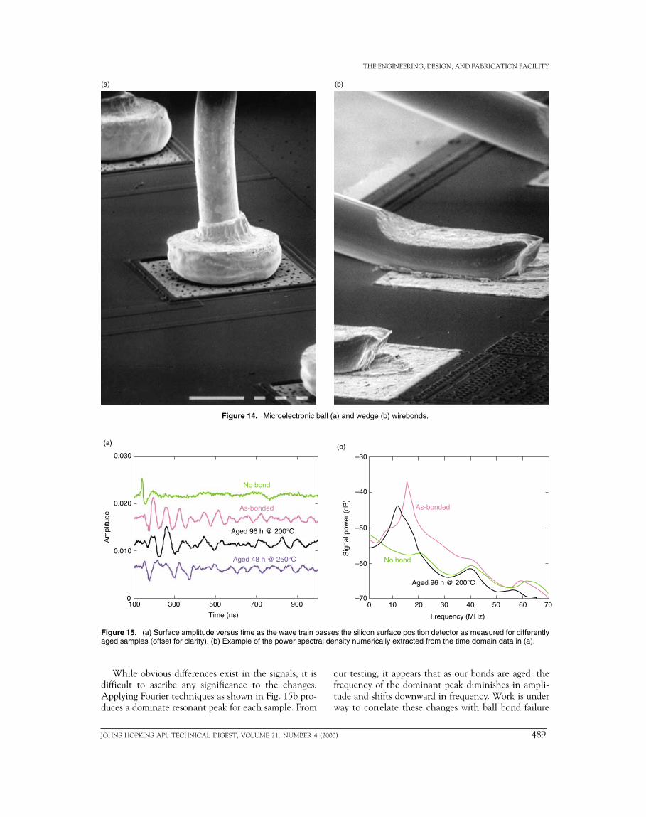
We are always exploring other techniques to quan-tify the quality of our delivered products. For example,we have used mechanical (wirebond pull32 and ballbond shear33) testing in conjunction with thermalaging techniques23 to determine the integrity of micro-electronic wirebonds (Fig. 14). Today, we are exploringa new laser-acoustic technique for determining bondquality.34 In this technique, a highly focused lasersource strikes the ball bond and causes a thermoelasticexcitation of the bond, which induces an ultrasonic oracoustic vibration to propagate in the substrate adja-cent to the bond. The surface wave portion of thisacoustic signal is sensed by a laser interferometer andused to determine bond quality. An example of theacoustic signatures with time for as-made and thermallyaged bonds is shown in Fig. 15a.
JOHNS HOPKINS APL TECHNICAL DIGEST, VOLUME 21, NUMBER 4 (2000) 489
THE ENGINEERING, DESIGN, AND FABRICATION FACILITY
(a) (b)
Figure 14. Microelectronic ball (a) and wedge (b) wirebonds.
While obvious differences exist in the signals, it isdifficult to ascribe any significance to the changes.Applying Fourier techniques as shown in Fig. 15b pro-duces a dominate resonant peak for each sample. From
our testing, it appears that as our bonds are aged, thefrequency of the dominant peak diminishes in ampli-tude and shifts downward in frequency. Work is underway to correlate these changes with ball bond failure
Figure 15. (a) Surface amplitude versus time as the wave train passes the silicon surface position detector as measured for differentlyaged samples (offset for clarity). (b) Example of the power spectral density numerically extracted from the time domain data in (a).
0.030
0.010
0.020
0100 300 500 700 900
Am
plitu
de
Time (ns)
No bond
As-bonded
Aged 96 h @ 200°C
Aged 48 h @ 250°C
(a)
–30
–40
–50
–60
–700 10 20 30 40 50 60 70
Frequency (MHz)
Sig
nal p
ower
(dB
)
No bond
As-bonded
Aged 96 h @ 200°C
(b)
H. K. CHARLES, JR., AND J. A. WEINER
490 JOHNS HOPKINS APL TECHNICAL DIGEST, VOLUME 21, NUMBER 4 (2000)
mechanisms such as the excessive growth of aluminum/gold intermetallics.
ISO 9001 in TSDISO 9000 is a set of standards for a quality assurance
system developed by the International Organization forStandardization.35 Nearly 100 countries have adoptedthese standards with only minor variations. From anAPL/TSD perspective, the most significant componentstandard is ISO 9001,36 which applies to organizationsinvolved in the development, design, manufacture,installation, and servicing of products. To satisfy therequirements of some sponsors and improve the qualityof our own internal processes, APL is working to be-come ISO 9001 compliant. The main proponents ofthis thrust are in the Space Department and TSD.
APL will be contractually required to be in compli-ance for many future NASA programs. On 8 June 1998,NASA’s Office of Safety and Mission Assurance issuedDirective NPD 8730.3, NASA Quality ManagementSystem Policy (ISO 9000). This document indicates that“where appropriate and beneficial,” NASA will requiresuppliers to comply with ISO 9000 or to be certified toISO 9001 by third-party examiners. At this time, allmajor NASA facilities have been certified to ISO 9001as required.
All impacted groups in TSD have completed aninternal audit to identify areas where we did not complywith the requirements of ISO 9001. The results of thisanalysis were entered into a database procured specif-ically for tracking compliance. Those data are onlineand are shared with the Space Department and othercognizant activities at APL. Estimates of the time andcost required to become compliant have been prepared,and many corrective actions have been implementedalready. Most of the improvements needed to complywith ISO 9001 require documentation of existing pro-cedures for which there are no written descriptions.
One of the most significant aspects of ISO 9001 isthe preparation, distribution, and control of processinginstructions. The standard covers all aspects of the taskof documentation, from initial sign-off to archiving.Perhaps the most difficult yet most important require-ment is to ensure that only the most current versionof a document is available to those performing theprocess described.
As noted earlier, TSD has nearly 200 fabricationstandard processes and procedures29 that describe virtu-ally every process used in the fabrication, assembly, andtesting of electronic and mechanical hardware. All ofthese have been converted to electronic format and areavailable on an internal APL Web site. Subject and titleindexes are also included in the online version. Thesedocuments are retrievable from anywhere within APL.
TSD will continue to make improvements and doc-ument processes until we can be assured of ISO 9001
compliance. Hopefully, this will occur during calendaryear 2000.
Work Flow TrackingThe EDF is committed to effectively tracking work
progress and monitoring job costs on all of its projects.To aid in these important tasks, we have recentlyacquired and implemented a computerized work track-ing system, VISUAL Manufacturing (VM) softwarefrom Lily Computers, a powerful tool for schedulingand estimating in a manufacturing environment. VMis a network-based management information systemdesigned for custom and mixed-mode manufacturing,as is the norm in TSD. It utilizes a fully relationalOracle database, and data can be retrieved and ana-lyzed in multiple ways.
Service-specific routings, coupled with master engi-neering flow documents, define the logical sequence oftasks to be performed. Estimates are made to reflect theeffort needed to complete each step of the work. Theroutings and flow control documents accompany thework in the form of a “traveler” and ensure that theproper steps are performed.
Required resources, both labor and equipment, areidentified for each step. Allocation and balancing ofthese resources across all tasks provide a means to pre-dict the need for additional resources. Early processplanning with the customer ensures that the require-ments of the program over its full duration can besatisfied before beginning work.
Data are collected via terminals throughout the EDFusing either a customized Web-based entry screen orautomated bar coding. Material and service costs arecollected and recorded for each step. Services procuredexternal to the EDF (e.g., painting, carpentry) are alsotracked and recorded. Job status and accumulated costsare available in real time and can be monitored throughthe APL internal Web server using preformatted reports.Full historical documentation is archived and readilyavailable for use as a baseline to estimate future work.
As labor hours are charged against the work inprogress, VM collects and compiles information relat-ing to both schedule and financial status. Data aregathered on who performed a specific task, how muchtime was charged to the task, the date the task wasperformed, and whether a milestone was completed.These data are compared to the estimated duration andscheduling of each step to determine if the work isproceeding on time and at cost. The progress of anyEDF task can be tracked as work is completed andcompared with the preestablished cost estimate andschedule.
VM is applicable to any task: simple or complex,fabrication or engineering, analysis or design. Its rout-ings are capable of providing a tree-like hierarchical

JOHNS HOPKINS APL TECHNICAL DIGEST, VOLUME 21, NUMBER 4 (2000) 491
THE ENGINEERING, DESIGN, AND FABRICATION FACILITY
structure that represents a drawing package of interre-lated products. This interrelationship in the systemleads to improved communications across groupboundaries and ties together EDF’s very diverse disci-plines. With both service providers and customershaving access to the same data, communication isvastly improved and customer satisfaction enhanced.This software greatly increases our capability to oper-ate competitively by allowing TSD to respond to ourcustomers’ needs more effectively, better predict andmonitor costs, and use resources more efficiently.
MetrologyDuring 1999, APL owned approximately 3000
pieces of electronic, physical, and dimensional testequipment categorized as Class 1. As such, they wereroutinely scheduled for calibration.37 In addition,there were over 10,000 items of test and measurementequipment (T&ME) that were categorized as Class 2.Class 2 T&ME is calibrated and repaired on an as-needed basis, but receives the same level of attention.
The Metrology Office is responsible for administer-ing the APL calibration program,37 coordinating ex-ternal and internal calibration and repair activities,and supporting those APL groups that perform special-purpose T&ME calibration and repair. The office ischarged with ensuring that all Class 1 measurementsare made with equipment that is traceable to standardsmaintained at the National Institute of Standards andTechnology or to natural physical constants. In addi-tion, the office must see to it that T&ME equipmentis calibrated on a fixed schedule and that properdocumentation of these calibrations and repairs ismaintained.
Historical records are kept to help determine ifequipment should be considered for replacement ow-ing to being out of calibration too often. The Metrol-ogy Office provides recall and overdue informationto APL Instrument Coordinators so that Class 1items can be submitted for calibration in accordancewith the published recall interval. It also providesnotification to users when Class 1 equipment is foundto be out of tolerance when received for calibrationso that the impact on measurements and tests per-formed since the equipment’s previous calibrationcan be determined.
The Metrology Office is located in Building 16 andoccupies approximately 74 sq. meters. It includes atechnical library, an equipment staging area, and ad-ministrative support. The office maintains a comput-erized calibration management system and the associ-ated hard copy records for every calibration and repair.It also provides assistance and guidance in the calibra-tion, repair, acquisition, operation, and interpretationof T&ME to all APL groups. The technical library
includes operation and service manuals for a large seg-ment of APL’s electronic T&ME. This collection isavailable to all T&ME users at the Laboratory and isalso occasionally used by the outside facility contractedto perform calibration and repair services.
The Metrology Office was established in 1993,when APL’s Calibration Laboratory was disestablished.Since then, virtually all of the calibration and repairwork has been subcontracted to outside facilities. Thishas resulted in an annual cost saving of approximately$400,000 when compared to the 1992 CalibrationLaboratory budget. As a further means to reduce op-erating costs, T&ME users have been requested tocontinuously evaluate their equipment and to submitonly those items for calibration that are used for Class1 measurements. In this way, equipment that is nolonger being used, or is not being used to make Class1 measurements, can be reclassified as Class 2. This hasallowed the annual number of calibrations performedto be reduced from 5629 in 1992 to only 2092 in 1998,a reduction of 63%.
In addition, users have disposed of, replaced, ordowngraded their unstable T&ME so that out-of-toler-ance items have decreased from 3.3 to 0.7%. Theseactions have reduced the potential for suspect data andthe cost associated with Out-of-Tolerance Alerts. TheMetrology Office also now sends Instrument Coordina-tors a mid-month notification of equipment due forcalibration in the following month, which helps keepthe number of overdue items down; overdue items havedecreased from an average of 364 in 1994 to 42 in 1998.
The Metrology Office has also implemented a newproperty and calibration management software system.With this system Instrument Coordinators can accessthe status of calibration and repair activities as well ascalibration history via the APL intranet.
SUMMARYThe EDF performs complex and dynamic electronic,
electromechanical, and mechanical hardware designand fabrication services which range from initial con-cept development to the delivery of fully tested andqualified hardware products. Such services have beenprovided by the EDF and its predecessors since theLaboratory’s inception.38 The ability to design, fabri-cate, and test hardware in-house has always been adistinctive feature of APL, and has set it apart fromsimilar university and government facilities. Buildingupon the extensive modernization and building pro-grams of the 1980s and early 1990s, the Laboratorycontinues to make significant investments in the EDF.Such investments are necessary to ensure that resourcesfor modern electronic and mechanical design and fab-rication continue to be in place for APL and its spon-sors during the 21st century.
H. K. CHARLES, JR., AND J. A. WEINER
492 JOHNS HOPKINS APL TECHNICAL DIGEST, VOLUME 21, NUMBER 4 (2000)
REFERENCES1Directory of Services for the Technical Services Department (TSD), JHU/APL,Laurel, MD, pp. 1–6 (Apr 1999).
2“Legacy of Transit” issue, Johns Hopkins APL Tech. Dig. 19(1) (1998).3Emch, G. F., “Air Defense for the Fleet,” Johns Hopkins APL Tech. Dig. 13(1),39–56 (1992).
4Cutchis, P. N., Hogrefe, A. F., and Lesho, J. C., “The Ingestible ThermalMonitoring System,” Johns Hopkins APL Tech. Dig. 19(1), 16–21 (1998).
5Technical Services Department Hardware Configuration Management Manual,TSD-TSD-400.1, JHU/APL, Laurel, MD (Sep 1993).
6Charles, H. K., Jr., “The Engineering, Design, Fabrication, Testing, andQualification Process Within the Steven Muller Center for AdvancedTechnology,” Johns Hopkins APL Tech. Dig. 12(1), 4–13 (1991).
7Charles, H. K., Jr., Wagner, G. D., and Abita, J. L., “Microelectronics at APL:30 Years of Service,” Johns Hopkins APL Tech. Dig. 11(1–2), 123–126 (1990).
8Chen, A. F., Farquhar, R. W., and Santo, A. G., “NEAR Overview,” JohnsHopkins APL Tech. Dig. 19(2), 95–106 (1998).
9Kusnierkiewicz, D. Y., “A Description of the TIMED Spacecraft,” in Conf.Proc. 387 Am. Inst. Phys., Part One, pp. 115–121 (1997).
10Anderson, V. C., “Digital Array Phasing,” J. Acous. Soc. Am. 32, 867 (1960).11South, H. M., Cronin, D. C., Gordon, S. L., and Magnani, T. P.,
“Technologies for Sonar Processing,” Johns Hopkins APL Tech. Dig. 19(4),459–469 (1998).
12Charles, H. K., Jr., “APL’s Packaging Future: The Next Few Years,” JohnsHopkins APL Tech. Dig. 20(1), 101–110 (1999).
13Charles, H. K., Jr., and Uy, M. E., “Design Aid for Multichip Modules,” inProc. Int. Microelectronics Symp., Boston, MA, pp. 42–48 (15–17 Nov 1994).
14Charles, H. K., Jr., Barnhart, W. D., Van Rij, J., and Petek, J. M., “TheImpact of KGD and Module Repair on Multichip Module Cost,” in Proc. Int.Microelectronics Symp., Chicago, IL, pp. 373–387 (26–28 Oct 1999).
15Blum, N. A., Charles, H. K., Jr., and Francomacaro, A. S., “Multichip ModuleSubstrates,” Johns Hopkins APL Tech. Dig. 20(1), 62–69 (1999).
16Sadowsky, J., Abita, J. L., Aylor, R. P., Barney, G. A., Bohandy, J., et al.,“Safer Transit Travel for the Blind Using an Infrared Warning System,” JohnsHopkins APL Tech. Dig. 18(2), 315–323 (1999).
17Atalar, A., Kraitchman, D. L., Carkhuff, B. G., Lesho, J. C., Oscali, O., et al.,“Catheter-Tracking FOV MR Fluoroscopy,” in Magnetic Resonance in Medicine,Lippincott, Williams, and Wilkens, Philadelphia, PA, pp. 865–872 (1998).
18Charles, H. K., Jr., Beck, T. J., Feldmesser, H. S., Magee, T. C., and Pisacane,V. L., “Compact, High-Precision, Multiple Projection DEXA Scanner forMeasurement of Bone and Muscle Loss During Prolonged Space Flight,” inProc. 1st Biennial Space Biomedical Investigators Workshop, League City, TX,pp. 202–204 (11–13 Jan 1999).
19Clatterbaugh, G. V., Vichot, P., and Charles, H. K., Jr., “Some Key Issues inMicroelectronic Packaging,” Johns Hopkins APL Tech. Dig. 20(1), 34–49 (1999).
20Le, B. Q., Nhan, E., Maurer, R. H., Jenkins, R. E., Lew, A. L., et al.,“Miniaturization of Space Electronics with Chip-on-Board Technology,” JohnsHopkins APL Tech. Dig. 20(1), 50–61 (1999).
21Benson, R. C., Murphy, J. C., and Charles, H. K., Jr., “Miniature SensorsBased on Micromechanical Systems,” Johns Hopkins APL Tech. Dig. 16(3),311–318 (1995).
22Wagner, G. D., Falk, P. R., and Murphy, L. H., “Engineering, Design, andFabrication Facilities in the Steven Muller Center for Advanced Technol-ogy,” Johns Hopkins APL Tech. Dig. 12(1), 14–22 (1991).
23Charles, H. K., Jr., Mach, K. J., Edwards, R. L., Lehtonen, S. J., and Lee,D. M., “Wirebonding on Various Multichip Module Substrates andMetallurgies,” in Proc. 47th IEEE Electronic Components and Technology Conf.,San Jose, CA, pp. 670–675 (18–21 May 1997).
24Mechtel, D. M., Charles, H. K., Jr., and Francomacaro, A. S., “NoninvasiveLaser Probing: A Solution for Improving the Testability of Buried MCM-DCircuit Structures,” in Proc. 23rd Int. Microelectronics Symp., Chicago, IL, pp. 367–372 (26–28 Oct 1999).
25Mechtel, D. M., Charles, H. K., Jr., and Francomacaro, A. S., “ImprovingMultichip Module Testability Using Poled-Polymer Dielectrics,” PatentApplication, JHU/APL File No. 1388–002 (1999).
26Blum, N. A., and Charles, H. K., Jr., “CO2 Laser Machining at APL,” JohnsHopkins APL Tech. Dig. 9(4), 380–382 (1998).
27The Johns Hopkins University Applied Physics Laboratory Quality Assurance PlanCLO-9805, JHU/APL, Laurel, MD (Aug 1998).
28Technical Services Department: Electro-mechanical Hardware Workmanship Stan-dards Manual, TSD-STD-800.1, JHU/APL, Laurel, MD (Jan 1991).
29“TEO Standard 300.1,” in Fabrication Standard Processes and Procedures, JHU/APL, Laurel, MD (1990).
30Soldered Electrical Connections, NASA-STD-3739.3 (Dec 1997).31Foster, L. A., A Pocket Guide to Geometrics II: Dimension and Tolerancing
Reference, ANSI/AMSE Y14.5M-1982, 10th Ed., Addison-Wesley Publishing,Reading, MA (1986).
32ASTM Standard Test Method F-459-84(1995)el, “Standard Test Methods forMeasuring Pull Strength of Microelectronic Wirebonds,” in Annual Book ofASTM Standards, American Society of Testing and Materials, WestConshohocken, PA (1995).
33ASTM Standard Test Method F-1269-89(1995)el, “Test Methods forDestructive Shear Testing of Ball Bonds,” in Annual Book of ASTM Standards,American Society of Testing and Materials, West Conshohocken, PA(1995).
34Romenesko, B. M., Charles, H. K., Jr., Cristion, J. A., and Siu, B. K.,“Microelectronic Wirebond Evaluation by Laser-Induced Ultrasonic Energy,”in Proc. 2000 Int. High Density Packaging and MCM Conf., Denver, CO (24–28 Apr 2000) (in press).
35International Standards Organization Web site, available at http.//www.iso.ch/9000e/9k14ke.htm (accessed 12 May 2000).
36Quality Systems—Model for Quality Assurance in Design, Development, Produc-tion, Installation, and Servicing, ANSI/ASQC Q9001-1994, American Societyfor Quality Control, Milwaukee, WI (1994).
37JHU/APL Test and Measurement Equipment Calibration Practices and Proce-dures, JHU/APL, Laurel, MD (Feb 1994).
38Van Allen, J. A., “My Life at APL,” Johns Hopkins APL Tech. Dig. 18(2),173–177 (1997).
ACKNOWLEDGMENTS: The authors gratefully acknowledge the efforts of allEDF personnel whose hard work and dedication have made possible the productsand services described in this article. Similarly, Mrs. S. Lynn Hoff is cited for herefforts in manuscript preparation. A special thank you is given to both E. J. Hoffmanand B. G. Boone who reviewed the manuscript and made many helpful suggestionsto improve both its quality and scope.
THE AUTHORS
HARRY K. CHARLES, JR., holds a B.S. and Ph.D. in electrical engineering fromDrexel University and JHU, respectively. He is a member of the APL PrincipalProfessional Staff and Assistant Department Head for Engineering in TSD. Dr.Charles has worked for over 25 years in microelectronics, specializing inelectronic devices, systems, packaging, and reliability. He is a Fellow and formerPresident of IMAPS, an IEEE Fellow, and a member of the Board of Governorsof IEEE’s CPMT Society. He has received international recognition for hisresearch, development, and teaching activities, including ISHM’s TechnicalAchievement Award (1987), Maryland’s Distinguished Young Engineer (1989),JHU’s Outstanding Teaching Award (1992), the CPMT Board of Governors’Outstanding Service Award (1992), ISHM’s Distinguished Service Award (1994),and the IMAPS Daniel C. Hughes Memorial Award (1998). Dr. Charles haspublished over 160 papers on electronic devices and packaging and has receivednumerous awards for best papers. His e-mail address is [email protected].

JOHNS HOPKINS APL TECHNICAL DIGEST, VOLUME 21, NUMBER 4 (2000) 493
THE ENGINEERING, DESIGN, AND FABRICATION FACILITY
JOEL A. WEINER received a B.S. in chemistry from Brooklyn College of theCity University of New York in 1970, an M.S. in chemistry from RutgersUniversity in 1974, and an M.S. in technical management from JHU in 1987.Before coming to APL in 1982, he was a Research Associate at RCA’s DavidSarnoff Research Center, and then Director of Product Technology forTechnics, Inc. Mr. Weiner is currently the Quality Assurance and Improve-ment Manager for TSD and a member of the APL Principal Professional Staff.He also served as Assistant Supervisor for the Microelectronics Group and theElectronic Fabrication Group. He has an extensive background in qualityassurance, high-reliability electronic assembly, thin film material science, andchemical processing for semiconductor and electronic fabrication. Mr. Weinerhas published or presented over 50 papers and holds 4 U.S. patents. His e-mailaddress is [email protected].