t ransv erse beam pr oles - cern document server · t ransv erse beam pr oles e. br avin ... nected...
TRANSCRIPT
Transverse beam profiles
E. BravinCERN, Geneva, Switzerland
AbstractThe performance and safe operation of a particle accelerator is closely con-nected to the transverse emittance of the beams it produces. For this reasonmany techniques have been developed over the years for monitoring the trans-verse distribution of particles along accelerator chains or over machine cycles.The definition of beam profiles is explained and the different techniques avail-able for the detection of the particle distributions are explored. Examples ofconcrete applications of these techniques are given.
1 IntroductionBefore discussing the details of beam profile measurements it is essential to understand what we meanby beam profiles. In the following sections the concepts of transverse planes and beam profiles willtherefore be explained.
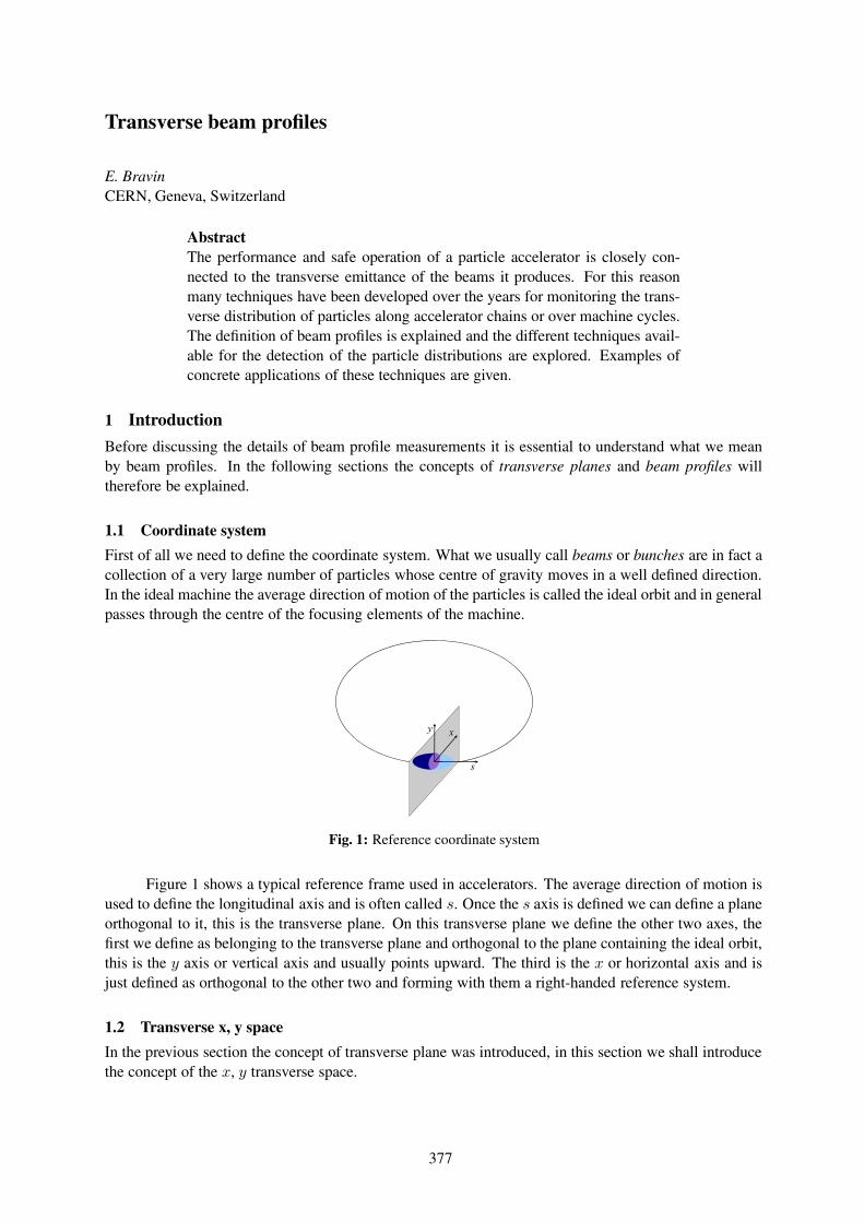
1.1 Coordinate systemFirst of all we need to define the coordinate system. What we usually call beams or bunches are in fact acollection of a very large number of particles whose centre of gravity moves in a well defined direction.In the ideal machine the average direction of motion of the particles is called the ideal orbit and in generalpasses through the centre of the focusing elements of the machine.
Fig. 1: Reference coordinate system
Figure 1 shows a typical reference frame used in accelerators. The average direction of motion isused to define the longitudinal axis and is often called s. Once the s axis is defined we can define a planeorthogonal to it, this is the transverse plane. On this transverse plane we define the other two axes, thefirst we define as belonging to the transverse plane and orthogonal to the plane containing the ideal orbit,this is the y axis or vertical axis and usually points upward. The third is the x or horizontal axis and isjust defined as orthogonal to the other two and forming with them a right-handed reference system.
1.2 Transverse x, y spaceIn the previous section the concept of transverse plane was introduced, in this section we shall introducethe concept of the x, y transverse space.
377

Consider a transverse plane, i.e., a plane orthogonal to the beam motion and every time a particlecrosses this plane we take note of the x and y coordinates of the particle. We then transfer these pointsonto a 2D chart and obtain the particle distribution in the x, y space as shown in Fig. 2.
Fig. 2: Particle distribution in the transverse x, y space
If there is no coupling between the motion of the particles in the x and in the y direction thisdistribution will be somehow elliptical with the axes of the ellipse parallel to the x and y axes.
1.3 Transverse phase spaceAs already mentioned before, a beam consists of many many particles whose centre of gravity moves ina well defined direction describing the ideal orbit. In fact each particle of the beam moves in a slightlydifferent direction, see Fig. 3, and focusing elements are necessary to keep the particles close together.
Fig. 3: Each particle in a beam moves in a slightly different direction
The velocity vector of each particle can be decomposed into two components: one parallel to thebeam direction s, and one orthogonal to it, the transverse velocity. The transverse velocity can in its turnbe decomposed into two more components: one along x and one along y as shown in Fig. 4.
As in the previous exercise we can assume a transverse plane and this time when a particle crossesit we note not only the x and y positions, but also the transverse component of the velocities, vx and vy.
Fig. 4: Decomposition of the velocity vectors into longitudinal and transverse components
In the previous exercise we used one 2D chart to plot the points, this time we need two charts, onone we plot for each particle a point corresponding to the x position and the vx velocity component, andon the second we do the same for the y components. For convenience we replace the notation vx, vy withx′ and y′. Figure 5 shows a sketch of typical transverse phase space distributions.
The particle distributions in the phase space are again of elliptical shape, but this time the ellipsescan be tilted. Moreover the area of the surface that contains all the particles is an invariant, this means
2
E. BRAVIN
378

Fig. 5: Particle distribution in the transverse phase spaces
that if the same exercise is repeated at several locations around the accelerator the ellipses will havedifferent aspect ratios and different tilts, but the area will remain the same.
To avoid confusion it is worth clarifying that in a machine where there is no coupling betweenthe x and y axes (ideal machine) the two phase space distributions are completely independent. Andalthough the areas are invariant, the value is not necessarily the same for the x phase space and the yphase space.
Because these two areas are invariants of motion they constitute fundamental parameters thatdefine the quality of the beam. These areas are called emittance and more precisely horizontal emittance,indicated with εx, and vertical emittance, indicated with εy . In reality there are several definitions of theemittance, but in practice all are related to the area of these ellipses.
It is worth mentioning that there are processes that can modify the transverse emittances of a beam,like acceleration, blow-up and cooling, but these topics are outside the scope of this lecture.
1.4 Differences between x, y space and phase spaceAs we have seen, the x, y space and the phase spaces are different things and sometimes confusion arisesbetween the two when one first starts studying this subject.
The x, y space only contains the spatial information of the distribution of the particles in a beamand merges both x and y axis in a single chart, while the two phase spaces x, x′ and y, y′ contain boththe spatial and the velocity information.
The phase space contains the whole description of the state of the particle for that particular plane(initial conditions) and this is all that is required for calculating the subsequent motion of the particle inthe electromagnetic fields of the accelerator.
Despite being different things, there are also common points between the two spaces. In fact bothcontain the position information and thus they have common projections. If one projects any of these 2Ddistributions along the x or y axis one obtains exactly the same thing. So the projection of the x, y spacealong x is the same thing as the projection of the x, x′ space along x and the same can be said for y.
These common properties allow us to sample the beam distribution in one space and convert it tothe other by using beam dynamics theories. This is of great importance as sampling the x, y space ismuch easier than sampling the phase space, although what one really needs is the phase space.
In practice the sampling of the phase space in a direct way is not technically feasible and it isalways approximated by measuring a sequence of position distributions. Many different techniques,described in other lectures in this school, have been developed over the years to do this.
1.5 Beam profilesTransverse beam profiles are simply histograms expressing the number of particles in a beam as a func-tion of the transverse position, thus we have an horizontal profile expressing the number of particlesat different x positions and we have a vertical profile expressing the number of particles at different ypositions.
3
TRANSVERSE BEAM PROFILES
379

Theoretically these histograms could be considered as continuous functions expressing particledensities vs. position, in reality, given the discrete nature of particles and the discrete position binningof the sampling, any profile measurement consists of a 1D histogram. Considering the 2D distributionsintroduced early on, the profiles are simply the projections of these 2D plots along one axis.
Fig. 6: Different types of 2D distributions and relative transverse profiles: x, y transverse space (top left), trans-verse phase spaces (bottom left), transverse phase space with amplitude distribution profile (right).
In the continuous case we can define a 2-dimensional density function expressing the transversedistribution of the particles in the beam i(x, y) and the profiles are simply given by
ProfileH(x) =∫ +∞
−∞i(x, y)dy, (1)
ProfileV(y) =∫ +∞
−∞i(x, y)dx. (2)
In a real case the integration limits can of course be reduced to the size of the beam pipe. Typicallythe particles are distributed according to the Gaussian function
i(x, y) =N0
2πσxσye−„x2
2σ2x
+ y2
2σ2y
«
, (3)
and thus we have
ProfileH(x) =N0√2πσx
e− x2
2σ2x , (4)
ProfileV(y) =N0√2πσy
e− y2
2σ2y . (5)
There is also another type of transverse profile that is sometimes used: it is called the amplitudedistribution and it represents a distribution in the phase space. In a circular machine, turn after turn the
4
E. BRAVIN
380

particles will describe ellipses in the phase space of different amplitudes, but the same ellipticity and tilt,it is thus possible to define an amplitude parameter (think of the equivalent of a radius) and define thedensity of particles as a function of this radius (amplitude). This type of sampling is performed usingscrapers and requires recording either the beam losses or the beam current decrease as a function of thescraper position while moving the scrapers into the beam. Figure 6 shows a sketch of the different 2Ddistributions and the relative profiles.
2 Sampling of distributions2.1 Intercepting vs. non-interceptingThe methods used to sample the distributions of particles in a beam can be divided into two main cate-gories: intercepting and non-intercepting. As the names suggest, in the first group we have the methodsthat require placing an object on the beam path and analysing the signal produced by the interaction ofthe particles with the object, in the second group we have the methods that use signals emitted spon-taneously by the beam. An exception to this definition is the laser wire scanner which is classified asnon-intercepting even though it requires an external stimulus (laser beam), nevertheless, given the ex-tremely small perturbation that this stimulus has on the beam, it is neglected. Among the interceptingtechniques there are:
– scanning wires– wire grids– radiative screens
and among the non-intercepting:
– synchrotron light– rest gas ionization– (inverse) Compton scattering– photo dissociation
2.2 Interaction of particles with matterThe most used techniques for sampling profiles are based on intercepting methods; the understanding ofthe interactions between the particles and the obstacles used in the sampling is essential.
There are many physical effects that can be exploited for the detection:
– ionization– creation of electron–ion pairs– secondary electron emission (SEM, low energy)– emission of photons
– elastic and inelastic scattering– dislocations– production of secondary particles (high energy)
– Cerenkov radiation– bremsstrahlung– optical transition radiation (OTR)
5
TRANSVERSE BEAM PROFILES
381

2.2.1 Energy depositionThe study of the energy deposited by the particles in our sensor (the object or obstacle we introduce onthe beam path) has two important uses:
– Signals are often proportional to the amount of energy deposited in the material (or more often thedensity of the energy deposition).
– The deposited energy can be dangerous for the sensor and can destroy it, again the total energyand the energy density are both important.
The mechanism of the energy deposition of charged particles in matter in the range in which weare interested is well described by the Bethe–Bloch formula which gives the energy deposition densityas a function of particle charge, particle momentum and material properties:
−dEdx
= Kz2Z
A
1β2
[12ln
2mec2β2γ2TmaxI2
− β2 − δ(βγ)2
]. (6)
The Bethe–Bloch formula does not describe the amount of energy deposited in the material, butthe amount of energy lost by the primary particle. This has an important consequence for our purposesas often our sensors are very small and absorb only a small fraction of the energy lost by the particle intraversing it. Think, for example, of the case of thin metallic foils traversed by high-energy electrons,many X-rays will be produced but only a negligible fraction of the energy of the X-rays will be reabsorbedin the foil.
The quantity widely used to describe the energy deposition is the dE/dx. This quantity describesthe amount of energy lost by a particle in traversing a unit length of material, often this quantity isnormalized for the material density and the units become thus MeV cm2/ g.
The dE/dx curve (an example is shown in Fig. 7) has been found to be almost independent ofthe material properties and the particle type (for q = ±1 elementary particles) provided one uses theparticle momentum and not the particle energy (it is the speed of the particle that matters in the ionizationprocess). The only parameter of the material important for the energy deposition is the density and if thedE/dx is normalized for it it disappears.
An important aspect to notice is that at low momentum the dE/dx is much larger, this means thatfor low-energy beams we can expect larger signals, but also more important thermal problems.
Looking at the dE/dx curve we notice that the dE/dx increases rapidly at very low particleenergies, reaches a maximum for βγ ∼ 0.02, then decreases rapidly and reaches a minimum for βγ ∼ 4(minimum ionising particle MIP); from there on it increases only slowly (not considering the radiativepart). As a reference, βγ = 0.02 corresponds to protons of 188 keV and electrons of 100 eV kineticenergy and βγ = 4 corresponds to protons of 2.9 GeV and electrons of 1.6 MeV kinetic energy. Fromthese values it is clear that in the field of instrumentation for particle accelerators the relevant part of thedE/dx curve is the one described by the Bethe–Bloch (again excluding radiative effects) that is valid forβγ > 0.05.
The main process occurring when a charged particle traverses a material is the creation of electron–ion pairs and the creation of excited states in atoms. The electron–ion creation is often used to detect thepassage of the particles, this is the case for example for ionization chambers and solid-state detectors.In these cases a bias voltage is applied across the material in order to attract the positive and negativecharges on opposite electrodes and measure the resulting current.
2.2.2 Secondary Emission (SEM)In the ionization process ion–electron pairs are produced all along the particle track, with a wide distri-bution of kinetic energy being transferred to the liberated electrons. In some cases the pairs are produced
6
E. BRAVIN
382

Fig. 7: The dE/dx curve for positive muons in copper, the same curve describes well other elementary particleswith q = 1 and different materials. Note that the horizontal axis is given in terms of particle momentum and notparticle energy. For reference, βγ = 1 corresponds to a kinetic energy of 212 keV for electrons and 390 MeV forprotons.
near the surface of the material and the electron has sufficient momentum and the right direction to reachthe surface. If the energy of the electron is larger than the surface potential barrier it may escape in thesurrounding vacuum as depicted in Fig. 8(a). This phenomenon can be amplified by biasing the materialwith a negative voltage, this will reduce the potential barrier at the surface and also prevent free electronsfrom being recaptured by the material.
Only a very thin layer near the surface of the material is involved in secondary emission, thismeans that it is not the bulk properties of the material that matter but the properties of the surface layer,commonly an oxide form of the bulk material that can be modified by the irradiation (ageing).
Usually SEM yields are measured experimentally for the different materials and different incidentenergies. Figure 9 shows such a measurement for protons on titanium and aluminium oxides togetherwith the analytical predictions based on the model described in Ref. [1]. As you can see, the measuredpoints fit very well with the prediction and nicely follow the dE/dx curve.
2.2.3 ScintillationThe ion–electron pairs produced by the passage of a charged particle will eventually recombine. Whenthis recombination happens, the binding energy of the electron will be emitted in the form of electro-magnetic radiation (photons). The passing primary particle will also excite atoms and molecules withoutionizing them, in this case, again, the return to the ground state is accompanied by the emission of pho-tons, see Fig. 8(b). The de-excitation process can involve many metastable levels and only a few of thetransitions will emit photons in a range suitable for observation, typically the visible range. The lifetimeof the excited states can vary over a large range and the emission can thus span over relatively longperiods and will depend on the properties of the material.
Special types of materials have been developed in order to obtain large light yields, these areusually referred to as phosphors and were primarily developed for the cathode ray tube industry. Table 1gives the compositions and the decay times for a few widely used phosphor types while Fig. 10 showsthe relative light emission spectra and emission efficiencies.
7
TRANSVERSE BEAM PROFILES
383

a) b)Fig. 8: A charged particle crosses a material and leaves behind a track of ion–electron pairs. a) Free electronscreated near the surface can have sufficient energy to reach the surface and escape the material. b) Excited atomsand molecules decay to lower levels emitting photons.
Fig. 9: Calculated and measured secondary emission yield for protons in different materials as function of protonkinetic energy.
Table 1: Composition and decay times of typical phosphor materials
Type Composition Decay time (of light intensity)From 90% to 10% From 10% to 1%
P 43 Gd2O2S: Tb 1 ms 1.6 msP 46 Y3Al5O12: Ce 300 ns 90 µsP 47 Y2SiO5 : Ce,Tb 100 ns 2.9 µsP 20 (Zn,Cd)S: Ag 4 ms 55 msP 11 ZnS: Ag 3 ms 37 ms
These phosphor materials have very large light yields, but can only be used as thin coatings onrigid substrates and can be easily damaged. Typical grain sizes for the coatings are of the order of themicron, this represents the ultimate resolution limit for the imaging device. These materials can only beused for very low-intensity and low-energy beams.
Ceramics materials, glasses, and crystals are much more frequently used in high-energy acceler-ators. The light yields are usually lower than for the phosphors, but the radiation hardness and thermo-mechanical properties are much better. A typical material widely used in accelerators is aluminium ox-ide, also known as alumina, doped with chromium (Chromox Al2O3 : Cr). This material is particularlyrobust and is well suited for the fabrication of beam observation screens.
8
E. BRAVIN
384

Fig. 10: Light emission spectra of typical phosphor materials
2.2.4 Cerenkov radiationCerenkov radiation is a form of electromagnetic radiation emitted by charged particles while movinginside a material. The emission process is linked to the polarization of the material and only takes placewhen the particles’ velocity is larger than the phase velocity of the light in that material. The thresholdvelocity is given by the formula
βt =1
n(ω), (7)
where βt = vt/c is the threshold value of the relativistic speed factor and n(ω) is the wavelength-dependent refraction index of the material.
Fig. 11: Cerenkov radiation is emitted by a particle travelling faster than the phase velocity of light in a material.The Cerenkov photons have a well defined angular distribution.
As the radiation is the result of the superposition of consecutive wave-fronts, the emission has avery particular angular distribution (see Fig. 11) with the photons emitted on the surface of a cone whoseaxis lies along the direction of motion of the particle and with aperture angle given by
cos θc =1
n(ω)β. (8)
The emission spectrum of the radiation is given by
d2N
dxdω=αz2
csin2 θc(ω) =
αz2
c
(1− 1
β2n2(ω)
). (9)
9
TRANSVERSE BEAM PROFILES
385

As an example of the intensity of the Cerenkov radiation, 10 photons are generated in the wave-length range λ ∈ [400, 500] nm by a relativistic electron (β ∼ 1) crossing a 1 mm thick quartz plate(nquartz = 1.46, θc ' 47). Because of the weak emission, relatively thick Cerenkov radiators are re-quired for beam imaging, this results in a limited spatial resolution. The light distribution at the exitsurface consists of an ellipse obtained by the intersection of the Cerenkov emission cone of the particleat the entrance in the material and the plane of the exit surface. In diagnostic systems the angles betweenthe radiator, the beam, and the detector need to be precisely aligned, for this reason it is important to takeinto consideration the refraction of the light at the exit surface.
2.2.5 Optical Transition Radiation (OTR)Optical Transition Radiation, also known as OTR, is a form of electromagnetic radiation emitted by acharged particle when crossing a boundary between materials with different dielectric properties. Inmost practical cases this boundary consists in the separation between the vacuum of the beam pipe anda metallic foil. OTR has many similarities with bremsstrahlung; the primary charged particle induces amirror charge on the surface of the foil travelling in the opposite direction. When the primary chargeenters the material these two charges neutralize. The effect is the same as if the mirror charge had cometo a sudden stop. This radiation is called the backward emission because it is emitted in the directionopposite to the direction of the particle; more precisely, the radiation is emitted along the direction of thespecular reflection of the beam on the surface.
Similarly radiation is emitted when the primary particle exits the foil, in this case it is the suddenappearance of the real charge that emits the radiation called the forward emission, always emitted in thedirection of the particle independently of the angle between the particle and the surface.
OTR has a complicated angular distribution, a simplified description for γ 1 of the case of theboundary between vacuum and a material with infinite εr it is given by the formula
d2W
dΩdω≈ Nq2
π2c
(θ
γ−2 + θ2
). (10)
The angular distribution corresponds to a thick walled cone of aperture angle 1/γ and the emissionis characterized by a wide flat spectrum. For practical cases of metallic foils in vacuum (or air) one canstill use this formula as the εr of metals is very large for frequencies up to the plasma frequency of thematerial ωp (which is linked to the density of electrons in the material). Figure 12(a) shows the geometryof the emission while Fig. 12(b) shows the angular distribution, note the maximum at 1/γ.
a) b)Fig. 12: OTR radiation is emitted by a particle crossing a boundary between materials with different dielectricproperties (a). Angular distribution of the OTR photons (b).
In optical transition radiation the thickness of the radiator has no influence on the emitted radiation,it is thus possible to use very thin foils as radiators so that the perturbation to the beam is minimal.
10
E. BRAVIN
386

Similarly foils of materials with good thermomechanical properties can be used for the imaging of highdensity beams.
Another interesting characteristic of this type of radiation is that it is radially polarized, i.e., thepolarization vector of the photons lies in the plane defined by the beam path (or its specular reflection forthe backward emission) and the direction of the photons. The angular distribution of OTR has a strongdependency on the energy of the particle and more precisely on the relativistic factor γ. The intensity ofthe radiation is also influenced by the energy in a complicated way. The complete model describing thistype of radiation can be found in Refs. [2] and [3]. A simple description of the dependency of the totalOTR power as a function of the particle energy is given by
W ∝
β2 β 1ln 2γ γ 1
. (11)
For the wavelength range λ ∈ [400, 600] nm, an accurate calculation using the complete OTRmodel predicts∼0.3 OTR photons per electron for 50 MeV electrons (β = 1, γ = 98.8) and∼0.001 pho-tons per electron for 100 keV electrons (β = 0.55, γ = 1.2).
For the backward emission there is one more important issue. The emission process can be seenas if the photons are created in the direction of the primary particle just before the particle crossesthe surface of the foil and are then immediately reflected by the surface of the foil. In the reflectionmechanism the properties of the surface are essential in defining the intensity, the spectrum, and thedirection of the outcoming photons. If the surface is not perfectly flat this will distort the particularangular distribution, in the extreme case of a very rough surface the backward emission can becomeisotropic. The radiation spectrum is also affected as there is a cut-off frequency at which the surface doesnot reflect any more, generally the resulting spectrum will be given by the convolution of the primaryradiation and the wavelength-dependent reflection coefficient.
2.2.6 Synchrotron radiationAn effect that is not properly an interaction of charged particles with matter, but is very important intransverse profile measurements, is synchrotron radiation. From classical electrodynamic theory weknow that when a charged particle is accelerated it emits electromagnetic radiation, bremsstrahlung isprobably the most widely known effect of this type. In the bremsstrahlung case the radiation is emittedas a consequence of the charge being decelerated (i.e., reduction of energy), there is, however, anothertype of acceleration that does not imply a change in the energy of the particle, but a change of direction.
The radiation emitted by a charged particle when its trajectory is deviated without changing itsenergy is known as synchrotron radiation or synchrotron light. As the name suggests this effect was ini-tially observed in the bending magnets of high gamma circular machines, namely electron synchrotrons,but is in fact emitted any time the trajectory of a charged particle is modified. In accelerators the mag-netic field of the bending magnets is used to force the trajectory of the particles into a circular orbit, as aby-product synchrotron radiation is emitted. This radiation can be exploited for scientific purposes likein synchrotron light sources, or can be a nuisance since the energy carried by this radiation is subtractedfrom the energy of the particles.
The fraction of energy lost by the beam via synchrotron radiation can be very important andconstitutes a huge limitation on the maximum energy of electron synchrotrons. The Large Electron–Positron collider (LEP) at CERN, for example, accelerated counter rotating electrons and positrons up to100 GeV and the RF system had to restore at each turn about 3% of the energy of the beam that was lostby synchrotron radiation. The total irradiated power was of the order of 10 MW [4].
The power emitted by a charged particle in the form of synchrotron radiation inside a bendingmagnet is given by [5]
P =1
4πε0
23ce2γ4
ρ2. (12)
11
TRANSVERSE BEAM PROFILES
387

a) b)
Fig. 13: A charged particle emits synchrotron light while travelling inside a bending magnet (a). Spectrum of theradiation (b).
The photons are emitted with a strongly forward peaked distribution (arising from the relativistic trans-formation from the particle reference frame to the laboratory reference frame), the aperture of this dis-tribution is given by 2/γ. As a particle travels around an accelerator it will continuously enter and exitbending magnets. The radiation emission will therefore start at the entrance of the magnet, remain con-stant while inside the magnet and finally stop at the exit of the magnet. An observer looking from abovewould see the light continuously emitted as a fan (like a car driving round a bend at night) see Fig. 13.On the other hand, an observer looking into the beam pipe would only see a flash whose duration corre-sponds to the difference in travel time between the photons and the particle during the time it takes theparticle to be deviated by the angle 2/γ, see Fig. 13. If the same observer would look at the entrance/exitedge of the magnet (blue arrows on Fig. 14) he would see an even shorter pulse.
The spectrum of the synchrotron radiation can be obtained by Fourier-transforming the pulseshape. The pulse length inside the magnet is given by
τ =2ργβc− 2 sin
(1γ
)ρ
c≈ 4
3ρ
cγ3, (13)
with the typical frequency around
ftyp ∼1τ≈ cγ3
ρ. (14)
In beam diagnostics it is often preferred to build devices operating in the visible range, undersome conditions, however, the emission spectrum of synchrotron radiation from a bending magnet doesnot cover this range, in these cases the so-called edge radiation can be useful. The concept is that shorterpulses correspond to wider spectra and thus edge radiation extends to lower wavelengths compared tosimple dipole radiation; this trick is often used in high-energy proton machines where the synchrotronradiation just starts to be exploitable for diagnostic purposes.
If the bending magnet is replaced by a sequence of dipole magnets with alternating polarities, it ispossible to produce synchrotron radiation without significantly modifying the trajectory of the particle,typically a device with three poles is used and takes the name of wiggler magnet. This device is usuallyused where the important aspect is to force the beam to produce synchrotron light with no particularinterest in the properties of the radiation. If the device consists of a large number of regular periodsit takes the name of undulator; the particles instead of being just deviated will oscillate around thecentral trajectory. The resulting radiation will have a much narrower spectrum centred on a well defined
12
E. BRAVIN
388

wavelength defined by the undulator period length
λ ∝ λu2γ2
, (15)
and the emitted power isW ∝ B2
0γ2 , (16)
where B0 is the absolute magnetic field in the centre of the pole.
Fig. 14: The pulse length of the synchrotron light seen by an observer looking at the entrance/exit edge of themagnet is shorter than the pulse seen by an observer looking inside the magnet
2.2.7 Inverse Compton scatteringIn the theory developed by Compton [6, 7], the scattering of a high-energy photon on an electron at restis described. The case where the energy of the electron is much larger than the energy of the photon isusually referred to as inverse Compton scattering (Fig. 15).
In order to understand inverse Compton scattering, it is sufficient to move to the reference frameof the high-energy electron; in this reference frame what is observed is just the well known Comptonscattering with the electron at rest and the photon having a much higher energy. After this change ofreference the interaction can be calculated with the existing detailed mathematical model of Comptonscattering. After this it is sufficient to re-transform the resulting particles back to the laboratory referenceframe.
In inverse Compton scattering the energy of the photon gets a boost of the order of γ 2 at theexpense of the energy of the electron, and the direction of the emerging photon is peaked around thedirection of the electron. In Compton scattering there is a strong correlation between the energy lost bythe photon and the scattering angle. The same happens in inverse Compton scattering with the differencethat this time the photon gains energy and the relation between angle and energy is complicated by thetwo reference frame transformations.
In beam diagnostics the electron usually has high energy (typically in the GeV range) and thephoton is in the range from infra-red (IR) to ultra-violet (UV) (∼1 to 4 eV) where powerful lasers areavailable.
The total cross-section for Compton scattering, described by the Klein–Nishina formula, is rathersmall, of the order of 10−25 cm2 for electrons [8], but with modern lasers it is possible to obtain measur-able signals for electron/ photon (or positron/photon) collisions. Although this effect exists for protonbeams as well (usually called Compton scattering on protons), the cross-section is much smaller as itscales with the square of the rest mass and it is thus not possible to obtain sufficient signals.
2.2.8 Photo dissociationAnother interesting phenomenon concerning the use of lasers in beam diagnostics is photo–dissociationor photo–neutralization. In this case photons are used to detach the extra electron from negatively charged
13
TRANSVERSE BEAM PROFILES
389

Fig. 15: A low-energy photon interacts with a high-energy electron. A fraction of the energy of the electron istransferred to the photon in the process.
hydrogen ions (H−). This process can be facilitated by external electric or magnetic fields which, ifopportunely applied, reduce further the already small ionization potential.
This process has attracted a lot of interest recently as most new developments of high currentproton linear accelerators favour the use of H− beams. The reason for this is that the injection insidea downstream circular machine can be done by stripping the two electrons instead of using septa andkickers allowing what is called phase-space painting resulting in much more brilliant beams. Figure 16shows a schematic of photo-neutralization and how the different species can be separated for detection.
Fig. 16: A laser beam is used to free the extra electron on an H− ion resulting in a neutral hydrogen atom and afree electron travelling at the same speed. A dipole magnet is used to separate the three species emerging from theinteraction.
3 Sampling techniquesWe have just seen the different processes that can be used for the detection of particles and the samplingof distributions. Apart from intercepting vs. non-intercepting, there is one additional distinction that canbe made on sampling techniques, and precisely between one-dimensional sampling and two-dimensionalsampling.
While two-dimensional sampling allows the direct sampling of the transverse space, the 1D sam-pling only allows the acquisition of projections. To express this difference more clearly, think of a beamwhere coupling deforms the distribution of particles in the transverse space into a tilted ellipse (i.e., anellipse whose major and minor axes are not aligned with the x and y axes). If we use a 2D samplingdevice, i.e., we take a picture of the beam, we immediately observe it. On the contrary, if we use only 1Dsampling devices, i.e., we acquire projections, we will not notice that the ellipse is tilted, and this evenwhen acquiring x and y projections simultaneously.
In the particular case presented above, the problem could be solved by acquiring three one-dimension profiles, one along x, one along y, and the third at 45. In case of an arbitrary transversedistribution, a complex system with a large number of 1D projections can eventually disclose the fulldistribution (tomography). In many machines, however, especially high-energy circular accelerators, theshape of the distribution is known and the measurement of the x and y profiles is sufficient to define thescaling parameters (usually with a fit of the measured data to a model).
14
E. BRAVIN
390

In the one-dimensional sampling we have
– Wire scanners– Wire grids– Rest gas ionization monitors– Laser wire scanners
While in the two dimensional sampling we have
– Screens and radiators– Synchrotron radiation
3.1 Sampling projections3.1.1 Wire scannersThe principle of the wire scanner is rather simple and consists of moving a wire across the beam whilemonitoring a signal proportional to the number of particles interacting with the beam, see Fig. 17 andFig. 18. Certainly the wire has to be placed inside the vacuum chamber increasing the complexity ofthe system. The signal observed is usually either the secondary emission current (SEM) from the wire,or the flux of high-energy secondary particles downstream of the wire. The high-energy secondaries areoften detected with scintillators coupled to photomultiplier tubes (PMT). Neutral optical filters could beinterposed between the scintillators and the PMT in order to avoid saturating the PMT and increase thedynamic range.
The precision of the wire scanner is dominated by two aspects: the precision with which the wireis positioned and the precision of the acquired signal. The major problem in building a wire scanner is todesign a solid and stable mechanical support for the wire and an accurate mechanism for the movement.Frequently some sort of encoder or resolver is used to read the position of the wire support (fork).
The speed of the movement mechanism varies over a very large range depending on the appli-cation. On linacs or transfer lines where the beam consists of short pulses at low repetition rate, ahigh-speed device is not required as the measurement is performed by acquiring one sample on eachbeam pulse (usually < 100 Hz) leaving plenty of time to move the wire from one pulse to the next, forexample, 500 µm steps at 100 Hz correspond to a speed of 5 cm/s. On the other hand, in circular accel-erators where either the beam intensity is elevated or the energy of the machine is rapidly increasing, afast scan is essential (to reduce wire heating in the first case, and avoid energy smearing in the second).In these cases wire speeds of ∼ 20 m/s have been achieved (typical revolution frequencies in circularaccelerators exceed 1 MHz).
Overheating of the wire and consequent wire damage is the most common problem with wirescanners, see, for example, Ref. [9] for a detailed description.
Although there are deconvolution techniques that can help reduce the error introduced by thefinite size of the wire, it is better to keep the wire diameter much smaller than the size of the beam to bemeasured. For this reason very thin wires are used, in the range between ∼ 5 µm to ∼ 50 µm (of coursethicker wires are possible for large beams). The mechanical constraints imposed by the deformation ordamage of the wires is the main limitation for the speed. The deformation of the mechanics and of thewire are also the main source of error in fast wire scanners, for this reason all high resolution scannershave slow movements [10] [11].
The SEM signal is typically used with low-energy beams as in this case no energetic secondaryparticles are generated; this signal tends to be quite small and requires care in the acquisition. A seriousproblem with the detection of secondary emission is the fact that when the wire is heated above 1000C
15
TRANSVERSE BEAM PROFILES
391

Fig. 17: A thin wire is scanned through the particle beam while the secondary emission current, the signal froma calorimeter downstream, and the signal of the motor encoder are acquired simultaneously. Plotting either of theSEM or PMT signals against the encoder gives the beam profile.
Fig. 18: Different types of rotative and linear wire scanners
by the beam it starts emitting electrons by thermionic emission perturbing the measurement of the SEMcurrent.
The signal from high-energy secondaries is typically large due to the high gain of the scintilla-tor/photo tube detector. On the other hand, beam losses can pollute the signal and, more importantly,due to the geometry of the detector and of the beam line, the signal induced in the detector may dependon the position of the wire and direction of the particles, introducing distortions and aberrations in theprofiles.
The dimension of the wire has a direct impact on the signal strengths for both techniques; in thecase of SEM the signal is proportional to the radius of the wire (SEM is a surface effect only) while forthe high-energy secondaries the signal is proportional to the square of the radius as it is a volume effect.
3.1.2 SEM grids (wire harps)Wire harps are devices where a large number of fixed wires or strips are placed on the beam path, Fig. 19.In this case the high energy secondaries generated in the interactions between the beam and the wirescan not be used as it is impossible to distinguish from which wire the particles have been generated. Theacquisition of the secondary emission current from each individual wire is then the only possibility.
The advantage of a wire harp over the wire scanner is that it allows single-shot acquisitions andplacing several harps one after the other allows single-shot measurement of the different planes (x and
16
E. BRAVIN
392

Fig. 19: Schematics of a SEM grid system (left) and an example of profiles acquired simultaneously at threedifferent locations along an emittance measurement line (right)
Fig. 20: Pictures of a SEM grid assembly (left) and of damaged 50 µm tungsten wires (right)
y) and/or the acquisition of the same plane at different locations (a technique used to measure the beamemittance). Another advantage over the wire scanner is the absence of moving parts, apart from a slowactuator used to insert and retract the device if needed. The drawback is the need for a complicatedacquisition system with many channels and small signals and a limit on the spatial resolution as the wirespacing can hardly be reduced to less than a few hundred micrometres.
Typically the acquisition chain is composed of a head amplifier that sits as near as possible to thegrid, often an area with high radiation, followed by an integrator or signal conditioning circuit that sits faraway in a safe counting room, and finally a computer controlled ADC. This scheme requires one signalcable per wire over the distance from the device to the counting room and the cabling can easily becomethe most expensive part of the system. In order to reduce the costs, techniques have been developed forsending the signals over twisted-pair cables. Although this solution can cut the cabling costs by a largefactor it also introduces limitations on bandwidth and cross-talk.
The number of wires in segmented detectors like the SEM grids varies from system to system. Asa rule of thumb for Gaussian beams one can consider the maximum wire spacing to be half the beam σand the detector size at least four σ’s which means a minimum of eight wires. This rule is valid for aperfect Gaussian beam well centred. In reality a denser mesh and a larger detector is better. Typical realsystems range from 16 to 48 wires.
If the signal-to-noise allows, it is possible to acquire the signals from the wires at high speed andobserve the evolution of the profiles inside a beam pulse. Acquisition frequencies up to 100 MHz havebeen achieved. As with wire scanners the damaging of the wires is the most important failure and havingmany wires permanently in the beam increases the risk, Fig. 20. For the wire grids even a single brokenwire can prevent the whole system from functioning correctly as the damaged wire can short-circuitseveral neighbouring intact wires rendering them unusable.
One important detail for wire grids consists in avoiding that secondary electrons generated on onewire get reabsorbed by another wire as this would generate cross-talk between channels. To avoid thisproblem, clearing electrodes are installed around the device to generate an electric field whose lines pullthe secondary electrons away from the wires.
17
TRANSVERSE BEAM PROFILES
393

3.1.3 Ionization profile monitorOwing to the problem of wire damage, both the wire scanners and the wire grids can not be used inhigh intensity beams or in continuous monitoring in circular machines. In these cases non-interceptingdevices are needed and the ionization profile monitor has been developed precisely for these needs.
The ionization profile monitor (IPM) is based on the interaction between the beam and the rest gaspresent in the vacuum chamber, even in the best vacuum there are still ∼ 1013 ions/cm3. If the rest gasdensity is not sufficient it can be artificially increased locally with a small gas injection.
When the particles of the beam pass through the rest gas these ionize the atoms leaving behinda column of ions and electrons. The spatial distribution of these secondaries is the same as that of thedistribution of the primary particles. By detecting the distribution of the secondaries, it is thus possibleto reconstruct the distribution of the particles of the beam.
The detection of the secondaries is achieved by applying an electric field perpendicular to thebeam trajectory and to the plane to be observed; this field will accelerate the ions and the electrons inopposite directions. At a certain point, well clear of the beam path, a detector is installed that interceptsthe drifting particles and records their arrival position.
In fact there are two options for the IPM, detecting either the electrons or the ions; in principleby switching the electric field polarity one could switch from one particle to the other. In reality thesystems are optimized for one case or the other. In most cases the electrons are observed and in this casea magnetic field parallel to the electric field is required. The role of this magnetic field is to reduce thetransverse drift of the electrons due to their random initial velocity and the acceleration due to the spacecharge of the beam (radial electric field). The electrons will spiral around the magnetic field lines whilebeing pushed towards the detector by the electric field.
The detector can be a simple grid of collecting electrodes or an optical system based on a multi-channel plate and a phosphor screen.
The first type of detector is similar to a SEM grid, but instead of the SEM current it is the currentfrom the collection of the charges that is measured, like the anode current in a vacuum tube. A positivebias potential on the wires or strips is required in order to capture and retain the incoming low-energyelectrons and avoid SEM emission. In case of ions a negative voltage is applied and the signal is thesuperposition of charge collection and SEM.
The optical detector is based on the multichannel plate, an electron multiplier array that conservesthe spatial information. The amplified electrons are then accelerated toward a phosphor screen by meansof an electric field of a few kilovolts. Finally a video camera records the image formed on the screen (astripe). Figure 21 shows a sketch of an IPM system and the image acquired by the video camera whileFig. 22 shows the picture of a real device and related measurements.
Ionization profile monitors often suffer from artefacts in the measurement, the most importantbeing the tails arising from the transverse drift of the electrons or ions during their travel towards thedetector not being completely prevented by the magnetic field. More information on IPMs can be foundin Refs. [12] and [13].
3.1.4 Laser wire scannerAnother type of non-intercepting 1D profile monitor is the laser wire scanner. This device is based on theinverse Compton scattering (ICS) described before and is thus only available for electron and positronbeams.
The basic concept is quite simple and is depicted in Fig. 23, a powerful, well focused laser (referredto as the laser wire) is scanned across the beam to be measured, as is done in a traditional wire scanner.The photons of the laser interact with the high-energy electrons and create high-energy X-rays or γ-rays,with an energy boost of the order of γ2. A detector downstream detects the flux of those particles. By
18
E. BRAVIN
394

Fig. 21: Schematic of an IPM monitor (left) and the relative image observed on the electron detector (right)
Fig. 22: Picture of an IPM monitor at GSI (left) and example of measurements (right)
plotting the number of gammas against the position of the laser the profile of the beam is obtained.In order to detect the generated gammas it is necessary to separate them from the primary electron
beam, this is usually done by means of a dipole magnet. In circular machines this can be a bendingmagnet of the lattice, in linear machines or transfer lines a magnetic chicane may have to be addeddeliberately. When the energy of the particles is very high, it may be difficult to deflect them just forthe purpose of detecting the gammas. In this case either the LWS device has to be installed in a locationwhere the particles are already deviated from their linear trajectory for other reasons, or a differentdetection technique has to be used.
In the ICS process we have seen that a fraction of the energy of the particles is transferred tothe photons. This fraction can be very high for ultrarelativistic beams. As a consequence the electronsthat have interacted with the photons will have an energy much lower than the average energy of the
19
TRANSVERSE BEAM PROFILES
395

Fig. 23: Schematic of a laser wire scanner system (left) and detail of the laser focusing system (right)
beam, and are for this reason called degraded particles (degraded electrons). As the optics of the beamline is designed for the average beam energy, the degraded particles can not be transported very farand can be detected as beam losses, perhaps by sophisticated ad hoc calorimeters placed in optimizedlocations. In order to facilitate the collection of the degraded particles, additional magnetic systems maybe introduced.
When a laser beam is focused on a small spot the divergence of the photons becomes important andthe laser beam remains focused only over a short distance, limiting in practice the maximum usable lengthof our wire, this represents a major difference between the laser wire and a real wire. This limitationdepends on the size of the waist of the laser beam, the smaller the waist the shorter the focused lengthdefined by the Rayleigh length LR. On the other hand, lasers can be focused to very small spots, aboutone order of magnitude smaller than the thinnest wire and thus allow the measurement of very smallbeams.
The size of the waist of the laser is given by
σ0 =λf
DL= λf/# , (17)
where λ is the wavelength of the laser, f is the focal length of the lens (or lens system), and DL is theclear aperture of the lens system. The ratio f/DL is often referred to as the stop number in optics anddenoted by f/#.
The Rayleigh length represents the distance over which the laser spot size remains within√
2 ofσ0 and is given by
LR =2πσ2
0
λ. (18)
Laser wire systems usually require very powerful lasers as the cross section for the inverse Comp-ton process is quite small. Typical lasers used for these applications deliver several millijoules of laserpower in pulses of a few picoseconds. The quality of the laser beam is also very important as it affectsthe smallest waist size that can be attained and is usually expressed in terms of the M 2 factor, M 2 = 1denotes a pure monomode Gaussian beam.
One alternative to powerful lasers are optical cavities with high quality factor (Q) installed acrossthe beam under measurement. The laser needed in this case is much simpler, however, the optics set-upbecomes very complicated; Fig. 24 shows a schematic of such a system.
The optics used to focus the laser is another very delicate part of the system together with thescanning mechanism based on mirrors and precise actuators like piezoelectric actuators. An alternativeto the complex and costly scanning systems consists in moving the particle beam itself, but this requiresa very good control of the beam position, sometimes difficult to achieve.
20
E. BRAVIN
396

Fig. 24: Schematic of a laser wire scanner using an optical cavity around the electron beam instead of a high powerlaser. The system is installed on a damping ring so the electron beam can be considered practically continuous(left, KEK-ATF). Schematic of a compact laser wire using reflecting optics inside the vacuum chamber to focusthe laser and relative measurement (right, SLAC- SLC).
3.2 Two-dimensional sampling3.2.1 Scintillating screensEspecially during the commissioning of an accelerator or of a beam line, it is important to have thepossibility of acquiring two-dimensional distributions of the particles, or, in other words, it is necessaryto take a picture of the beam. As described earlier, 1D profiles can be sufficient to tune and characterizea particle beam if its overall properties are well known and understood. When this is not the case 1Dprofiles do not give enough information to allow identification of artefacts and problems. Scintillatingscreens are in fact one of the earliest used diagnostics in particle accelerators. Initially the screens wereobserved directly by human eyes, when the energy and intensity of the beams became dangerous, directobservation was replaced by TV cameras.
The principle of scintillating screens as described earlier is that charged particles traversing amaterial ionize and excite the atoms or molecules inside. Part of the energy deposited in the materialin this process is then returned under the form of light. On the screen, at each location, the amount oflight emitted is proportional to the number of particles that crossed it. For a monitor to work properlythe linearity between particle density and light emission is of the utmost importance.
Under the label of scintillating screens there are in reality a huge number of different devicesdesigned for different uses. In some cases thin coatings of light emitting materials (phosphors) aredeposited on rigid substrates, usually for low-energy and low-intensity beams; the substrate can also beglass offering the opportunity to look from the back side. More often the scintillating plates are rigidobjects made of some sort of ceramic, quartz, or monocrystals.
Among the most used ceramics it is worth mentioning aluminium oxide (alumina) and among themonocrystals YAG, a material also used in the fabrication of lasers. Often these materials are doped inorder to increase the light emission or shift the wavelength of the emission for a better coupling withthe light detector. In the case of alumina the most frequently used dopant is chromium and the materialgoes under the name of chromox. Alumina screens are by far the most used in particle accelerators. Thismaterial is in fact very robust both mechanically and thermally, has a very good light emission yield, andis relatively cheap.
A profile monitor based on scintillating screens is typically composed of the screen, an insertionmechanism, an illumination system, and a video camera for the detection as can be seen in Fig. 25. Asalready mentioned it is very important that the relation between particle density and acquired signal belinear. This means that the scintillating screen itself must have a linear curve of emission, but also thatthe detector must have a linear response and that no saturation occours. It is very frequently the case
21
TRANSVERSE BEAM PROFILES
397

Fig. 25: Schematic of a scintillating screen monitor
that the image detector becomes saturated leading to a distorted distribution. For this reason selectableneutral density filters in front of the camera are often used.
Scintillating screens are usually rather thick, of the order of one or more millimetres. The multiplescattering occurring inside the material increases the divergence of the beam and induces beam losses.This is the one of the reasons why the screens are inserted only when required and otherwise retracted.
Often the screen is installed at 45 to the beam and the camera at 90 as depicted in Fig. 25. Thissolution is convenient because it minimizes the longitudinal space required for the monitor and a roundbeam will appear round on the image, this is without considering the optical aberrations. In reality whenthe camera is not perfectly orthogonal to the screen a trapeze deformation of the image occurs, this isdue to the different distances between the screen and the camera at different locations on the screen.
Calibration marks on the screen can be very useful, provided they do not interfere with the mea-surements, as they help in identifying errors and can be used to develop correction algorithms [14](Fig. 26).
Another type of aberration on the image is caused by the finite thickness of the screen. As canbe seen in Fig. 27, the photons are emitted all over the volume traversed by the beam and the angle ofobservation has an effect on the image observed.
The best solution would be to have the screen orthogonal to the beam and the camera orthogonalto the screen, unfortunately this would mean having the camera or at least a mirror placed on the beampath. Observing the back side of the screen either directly (low energy machines) or using a mirror is atechnique used in some cases. A more general compromise is to tilt the screen at small angles (Fig. 27right), the drawback is that the longitudinal occupancy of the monitor on the beam line is increased, notalways a possibility.
3.2.2 Optical transition radiation screensThe scintillating screens described above have two main limitations: the linearity of the response curve,also due to saturation in the material, and the time persistency of the emission. As described already thelinearity is an essential condition for profile monitors. The decay time of the emission is usually lessimportant, but there are applications where a short slice of the beam, or a limited number of bunches,have to be acquired. In this case most scintillators would fail as a few microseconds is the fastest decay
22
E. BRAVIN
398

Fig. 26: Correction of geometrical aberrations due to the optics system and misalignment. Before correction (left)and after (right).
Fig. 27: Errors due to the finite size of the screen thickness: A indicates the desired observation while B indicatesthe real observation.
time available, and even in these fast materials the decay may be composed of many time constants somemuch longer than the few microseconds of the main emission line. Long decay times are often referredto as persistence and can be many seconds or even minutes.
In a previous section, the Cerenkov radiation was described and although it would solve the linear-ity and time response limitations of the scintillating screens, it poses more problems than it solves owingto the geometry of the emission.
However, a third type of radiation exists that can be used in place of the scintillating screens:optical transition radiation. OTR, described in a previous paragraph, is a surface emission (contraryto the volume emission of scintillation and Cerenkov), it has a characteristic angular distribution and isradially polarized. Figure 28 shows a schematic of an OTR system based on backward emission (forwardradiation could in principle also be used, but it is difficult to separate the light from the particles and forthis reason it is rarely used). Figure 29 shows an OTR station installed in TTF at DESY together with afew beam images acquired with this device.
Installing the camera just on the reflection direction of the beam would mean looking in the holeof the emission (centre of the cone) with almost no light in the aperture of the lens. The solution is toinstall the camera at a slightly different angle so that it is centred on the peak of the emission (portion ofthe OTR lobe). The angle of the OTR cone is 1/γ and thus the correct angle between the camera and thescreen and the screen and the beam, these are of course equal because of the mirror-like effect, is givenby
ϕ =12
(π
2± 1γ
). (19)
The fact that the emission is not isotropic can introduce artefacts in the image as particles hittingdifferent areas of the radiator or with different angles of incidence can have different acceptances (thefraction of emitted light collected by the camera). When designing an OTR system it is important tostudy this effect, optical simulation packages are very useful in this regard.
23
TRANSVERSE BEAM PROFILES
399

Fig. 28: Schematics of an OTR monitor, note how the angles between beam, screen and camera have to follow aprecise scheme
Fig. 29: Picture of an OTR station used at DESY and images acquired with this type of system on TTF. Note howthe complexity of the particle distribution could not be deduced from 1D profiles alone.
Another important parameter in OTR systems is the reflectivity of the radiator as we use thebackward emission. The surface properties of the radiator influence both the total amount of light,with the total reflection coefficient, and the angular distribution, a rough surface will diffuse the lightand smooth the peculiar OTR distribution. In some cases, for example when large screens are needed,the OTR radiator is purposely rough so as to smear the emission and obtain a more uniform angulardistribution. Another solution for these applications consists in using radiators with parabolic shapes; ifproperly designed, parabolic radiators can concentrate the emission towards the camera independentlyof the position on the screen.
Frequently OTR radiators are made with high-quality mirror surfaces, using either metallic foils orthin substrates coated with metallic depositions. The second solution often offers better mirror qualitieswhile the first reduces the amount of material on the beam path. Typical metallic foils are aluminium ortitanium down to a few micrometres thickness while typical metallized substrates are silicon or siliconcarbide a few hundred micrometres thick (like the wafers used in microelectronics). Aluminium or goldare frequently used as coating materials. Carbon foils are also used where high density beams have to beobserved thanks to the excellent thermal properties of graphite (Fig. 30 shows how a high density beamcan destroy a radiator), on the other hand the optical qualities are not quite perfect.
If the numerical aperture of the optical system is large enough, and this also depends on the γ ofthe beam, the whole OTR cone can be observed. In order to understand this better we shall look at apractical case. Figure 31 shows a simple optical system made of a single thin lens. We first define the
24
E. BRAVIN
400

Fig. 30: Picture of an OTR station used at KEK and images acquired with this type of system on ATF. The imagesshow the damage caused to the radiators (copper and beryllium) by the beam in only a few shots.
Fig. 31: Simple optical system composed of a single thin lens
magnification factor of the optical system based on the size of the beam to be observed and the size of thecamera sensor. Then we choose the distance between the object (the screen) and the lens, this is usuallylimited by the presence of the vacuum tank. At this point we can calculate all the remaining parametersof the optical system.
The magnification factor of the system m is given by
m =h′
h=s′
s, (20)
and using the lens maker formula1f
=1s
+1s′, (21)
we can deducef =
sm
m+ 1. (22)
We can use Eq. (22) to calculate the focal length for the lens and then Eq. (23) to calculate the lastunknown parameter, the distance between the lens and the camera
s′ =sf
s− f . (23)
In a practical case we can have s = 300 mm andm = 0.2 from which we can calculate f = 50 mmand s′ = 60 mm. In many cases we shall not use a single lens as this introduces aberrations, but an opticalsystem based on many lenses. In our example we assume the use of a ready-made camera lens. A goodCCTV 50 mm lens has f/# ∼ 1.4, from this we can calculate the lens diameter (being a complex lenssystem this is in fact the clear entrance aperture of the lens and not the physical diameter of the first lens)
D =f
f/#=
501.4
= 36 mm , (24)
and the acceptance angle at the centre of the screen
θ =D2
s=
36600
= 0.06 rad . (25)
25
TRANSVERSE BEAM PROFILES
401

We can now calculate the relativistic γ corresponding to this aperture for the OTR radiation:
γmin =1θ
=1
0.06= 17 . (26)
From Eq. (26) we obtain that for the setup of the example and for beams with γ larger than 17we can observe the whole OTR cone, i.e., we can centre the camera on the reflection axis of the OTRradiator, while for beams of lower momentum we have to centre the camera on one of the lobes asdescribed before.
3.2.3 Synchrotron light monitorsAnother way of sampling the two-dimensional distribution of the particles is offered by synchrotronradiation (SR). The advantage of synchrotron radiation over OTR is that it does not require a radiator.This means that there are no limitations on the particle densities that can be observed. Moreover it alsoallows the continuous observation of the beam profiles.
SR monitors are almost always designed around existing magnets, that is around magnets that arealready installed in the machine for other purposes. It may be necessary, however, to install dedicatedmagnets in order to overcome specific needs. For example, if the γ of the particle is too low, the spectrumof the emission from a lattice bending magnet can be concentrated in the infra-red and longer wavelengths, with important difficulties for detection. In a case like this a special magnet, called an undulator,can be used.
Undulators are periodic magnets in which the central wavelength of the SR emission depends onthe magnetic period. Undulators can also be used if the intensity of the emission is not sufficient as theycan be much more effective than a simple bending magnet in generating SR. Of course different beamconditions will require different solutions. It is important to keep in mind that even if an undulator isused as source a dipole magnet is still required to separate the light from the particles. Sometimes theedge effect in bending magnets can be used to shift the SR spectrum. The SR emission at the entranceand exit edges of the magnet is in fact slightly shifted towards shorter wavelengths since SR pulses areshorter there. In some cases this shift can be sufficient.
One of the biggest problems in building a SR profile monitor is the fact that the source is notwell defined. As the light is emitted in the interaction between the particles and the magnetic field,the particles will emit during the whole time they traverse the magnetic field region, this can be almostcontinuous in compact circular machines where bending magnets are very close to one another. Theresult is like taking the picture of a moving car at night on a bend, we see the trace of the car, but can notmake out the details of the headlights. In the case of the car it is possible to use a very fast shutter timeto compensate for the motion, in a SR monitor this is not possible as the light and the particles travelalmost at the same speed.
Another possibility is to use an angular selection and detect only photons that come from a par-ticular point, our source. To define an angle we usually need two slits, only photons with the right anglewill pass through both. In a SR monitor we can use the fact that the light is emitted in a very narrow conein the direction of motion of the particle and reduce the system to a single slit (Fig. 32).
Another important problem of SR is the diffraction. From optics we know that there is a preciserelation between the resolution of an optical system and the numerical aperture. The finite aperture intro-duces diffraction and the influence of the diffraction on the image increases as we reduce this aperture.
For an optical system the diffraction limited spot size (image plane) is given by
d = 2.44λf/# = 2.44λf
C.A. . (27)
26
E. BRAVIN
402

Fig. 32: Sketch of a synchrotron light monitor using a bending magnet as source. The source is delimited using anangular selection defined by the slit and the natural small opening angle of SR.
Using Eq. (22) we can write
D =d
m= 2.44λ
s
(m + 1) C.A. , (28)
where D is the diffraction limit in object space, m is the magnification factor, and s the distance betweenthe object and the lens. In our case the clear aperture (C.A.) is the size of the SR spot on the lens as theclear aperture of the lens is usually much larger. For the vertical plane the SR spot is just s/γ, for thehorizontal plane the definition is a bit more complicated due to the presence of the slit.
If we assume C.A. = s/γ we can rewrite Eq. (28) as
D = 2.44λγ
(m + 1). (29)
The important result of Eq. (29) is that the resolution of the synchrotron light monitor is propor-tional to λγ, this means that for high-energy particles we can have serious resolution limits that can onlybe solved by observing shorter and shorter wavelengths. For this reason, on electron machines wherehigh resolution is necessary, synchrotron light monitors based on the detection of soft X-rays have beenbuilt requiring the development of soft X-ray optics elements. Other techniques like deconvolution of thepoint spread function or interferometry allow one to extract useful information even when the diffractioneffects are important.
4 Light sensorsMany of the monitors described above are based on the detection of visible light. Light sensors can bedivided into two families:
– One-dimensional sensors– Photodiode array– Linear CCD– Segmented photomultiplier (multi-anode PMT)
– Two-dimensional sensors– Area CCD– Area C-MOS– Video tubes
27
TRANSVERSE BEAM PROFILES
403

4.1 One-dimensional sensorsOne-dimensional sensors are usually fast, with readout speeds up to hundreds of MHz. The readoutcan be of sequential or parallel type. In the second case each channel is read out independently and theacquisition chain requires as many channels as there are channels in the detector. The sequential typeinstead requires only one readout channel and the values of the channels of the detector are acquired oneafter the other using a multiplexing technique.
Usually photodiode arrays and multi-anode PMTs are of the parallel type while the linear CCDsare of the sequential type. The parallel type can only be used when the number of channels is limitedas the electronics and cabling would otherwise become too complex, typically up to 32 channels. Theadvantage of these devices is that they can be very fast, with acquisition rates up to 100 MHz. The linearCCDs on the other hand allow a large number of channels with a rather simple readout electronics.
CCDs with over 1000 channels are available, the readout speed is, however, much reduced andusually does not exceed 100 kHz depending on the number of channels (typical channel data rate is ofthe order of 20 MHz). Often linear CCDs allow the selection of the number of channels to be readdepending on the needs of the application. It is then possible to develop a detector that can switchbetween fast acquisition with few channels and slow acquisition with many channels.
In terms of sensitivity the multi-anode PMTs are superior to the other two devices as an amplifi-cation up to 105 takes place inside the device itself allowing the detection of single photons. The diodearrays and the linear CCDs have similar sensitivities and require a large number of photons for a goodsignal (∼50 000/channel).
The PMTs on the other hand are a bit more complicated to use as they require a high voltage bias(∼1000 V) and can be damaged by a high light intensity. PMTs are also very good in terms of radiationresistance, much better than the other two solid-state devices.
4.2 Two-dimensional sensorsTwo-dimensional detectors only have sequential readout as the minimum number of channels neededto acquire an image is already much too large for parallel readout (32 × 32 = 1024). Although 2Dsegmented photomultipliers and photodiode arrays exist, their granularity is usually very small and notmade for the acquisition of images (max. 8× 8).
There are two main families of solid-state 2D image sensors, CCDs and C-MOS. The differencebetween the two is that the CCD is a matrix of pixels (electron wells) that are shifted one after the othertowards the readout electronics while the C-MOS is a matrix of pixels each one directly connected viaa multiplexing system to the readout electronics. In principle the difference should not be importantfor normal acquisitions, in fact the CCD is just a silicon substrate with transparent electrodes on top,while the C-MOS device requires electronic components next to each pixel. The filling factor of the twodevices is thus quite different (fraction of the area of the detector that detects the impinging photons).The result is that the sensitivity can be very different and is typically a factor 10 less for C-MOS devicescompared to CCDs.
The advantage of the C-MOS is that any portion of the detector can be read out at will while onCCDs the whole matrix has to be read out.
Readout speeds of 2D devices are quite slow, typical sensors are designed for 50 Hz readout(25 Hz if one considers the interlaced acquisition often used in TV cameras). There are, however, specialdevices designed for higher acquisition speeds, typically based on C-MOS sensors as these allow oneto split the readout in several parallel blocks (called taps) and redefine the acquisition area (number ofpixels) depending on the required speed. Often the set-up is done at high resolution and low speed andthen the real acquisition is done at low resolution and high speed. These special cameras can attain speedsof the order of 100 kHz (105 frames per second). These special fast cameras can be used in turn-by-turnacquisition or pulse-by-pulse acquisition, usually observing OTR or SR.
28
E. BRAVIN
404

A 2D device that requires a special treatment is the video tube. Nowadays this technology isobsolete and it is quite difficult to find spare parts; it is, however, very important in particle acceleratorsas it is very tolerant of ionizing radiation. In many locations of our accelerators the radiation is too highfor devices like CCDs or C-MOS and the video tube is the only device that can acquire images of thebeam in these situations.
Many different types of video tubes were developed from the 1930s to the 1980s, then the solid-state detectors killed the industry. Some of them are of excellent quality and can deliver images notfar from that of CCDs. Unfortunately, the best video tubes are not radiation resistant and those that aredeliver images quite far from those obtained with solid-state devices.
The problem is complicated by the fact that not only the sensor but also the associated electronicshave to be radiation tolerant. The solution is to build tube-based cameras, using VIDICON or NUVICONtubes for example, with limited electronics on board, also based on vacuum tubes, and install the restof the required circuits far away in safe areas. This means that small and delicate signals have to travelover long cables reducing the quality of the images even more. The sensitivity of these cameras is muchlower than CCDs (between 10 and 100 times lower) and is normally used only together with scintillatingscreens. Problems with linearity both spatial and in intensity reduce the possibility of making seriousmeasurements with these systems, they are, however, very important as they give a visual feedback ofthe beam.
There is also another type of image sensor, similar to the C-MOS, the CID (charge injection de-vice). The CID offers similar results to C-MOS devices, with the advantage that radiation-hard versionsare available. These devices can be used in areas were radiation is moderated, usually rad-hard CIDcameras can stand up to 5 Mrad while CCDs and C-MOS only survive up to ∼ 100 krad.
4.3 Image intensifier
Fig. 33: Schematics of image intensifiers. The device on the left is equipped with one MCP while the one on theright is equipped with two MCPs mounted in chevron layout. Single MCP intensifiers have gains ∼ 102 whiledouble MCP devices can attain gains of ∼ 104.
In cases where the light intensity is not sufficient or in cases where a fast shutter is required (downto a few nano seconds) the image intensifier is used. The image intensifier is a device that convertsthe photons into electrons using a photocathode, then amplifies the electrons using a multichannel plate(MCP) and finally converts the electrons back into photons using a phosphor target, see Fig. 33. At eachstage the electrons are accelerated and guided using electric fields (several kV). By adding a fine mesh infront of the photocathode (gate electrode) it is possible to operate the image intensifiers as fast shutters.The best devices have gains of the order of 104 and can be gated to a few nanoseconds.
29
TRANSVERSE BEAM PROFILES
405

The core of the image intensifier is the multichannel plate or MCP, a device used also in manyother applications where amplification of electrons is required. Almost any type of charged particle canbe used as input to an MCP, the output is however always electrons, but in much larger numbers. TheMCP is a plate of high resistance material in which tiny holes are drilled in a matrix. When an electronstrikes the walls of these tubes more electrons are released via secondary emission, an electric fieldparallel to the tube axis accelerates these electrons that eventually strike the walls again producing moreamplification. At the end of many processes like this a single electron hitting the MCP is amplified tomillions of electrons.
AcknowledgementsI would like to thank all the people working in beam instrumentation as most of the material presented inthis lecture has been taken from many published documents. It is impossible to mention specific namesas there are so many involved.
References[1] R. G. Lye and A. J. Dekker, Theory of secondary emission, Phys. Rev. 107 (1957) 977–81.[2] V. L. Ginzburg and V. N. Tsytovich, Transition Radiation and Transition Scattering (Hilger,
Bristol, 1990).[3] L. Wartski, J. Marcou, and S. Roland, Detection of optical transition radiation and its application
to beam diagnostics, 5th IEEE Particle Accelerator Conference, San Francisco, CA, USA, 1973,pp. 544–8.
[4] J. M. Jowett, Beam Dynamics at LEP, CERN-SL-98-029-AP, CERN, Geneva, 1998.[5] A. Hofmann, Synchrotron radiation from the large electron–positron storage ring LEP, Phys. Rep.
64 (1980) 253–81.[6] A. H. Compton, The spectrum of scattered x-rays, Phys. Rev. 22 (1923) 409–13.[7] A. H. Compton, A general quantum theory of the wave-length of scattered x-rays, Phys. Rev. 24
(1924) 168–76.[8] D. Fargion, R.V. Konoplich, and A. Salis, Inverse Compton scattering on laser beam and
monochromatic isotropic radiation, Z. Phys. C74 (1997) 571–6.[9] M. Sapinski, Model of Carbon Wire Heating in Accelerator Beam, CERN-AB-2008-030-BI,
CERN, Geneva, 2008.[10] H. Hayano, Wire scanners for small emittance beam measurement in ATF, 20th International
Linear Accelerator Conference, Monterey, CA, USA, 2000, MOC01.[11] G. Arduini, B. Dehning, G. Ferioli, J. Koopman, D. Kramer, and F. Roncarolo, Accuracy of Profile
Monitors and LHC Emittance Measurements, CERN-LHC-Project-Report-782, CERN, Geneva,2004.
[12] K. Satou, N. Hayashi, S. Lee, and T. Toyama, A prototype of residual gas ionization profilemonitor for J–PARC RCS, 10th European Particle Accelerator Conference, Edinburgh, UK, 2006,pp. 1163–5.
[13] P. Forck, A. B. Bank, T. Giacomini, and A. Peters, Profile monitors based on residual gasinteraction, 7th DIPAC, Lyons, France, 2005, pp. 223–7.
[14] E. Benedetto and E. Bravin, Calibration and Correction of the BTVs Images,CERN-AB-Note-2008-024, CERN, Geneva, 2008.
30
E. BRAVIN
406