system integration of electronic functionality in packaging
TRANSCRIPT

Thesis for the degree of Doctor of Technology, Sundsvall 2011
SYSTEM INTEGRATION OF ELECTRONIC FUNCTIONALITY IN PACKAGING APPLICATION
Tomas Unander
Supervisors:
Hans‐Erik Nilsson
Bengt Oelmann
Electronics Design Division
Department of Information Technology and Media
Mid Sweden University, SE‐851 70 Sundsvall, Sweden
ISSN 1652‐893X
Mid Sweden University Doctoral Thesis 112
ISBN 978‐91‐86694‐49‐4
Akademisk avhandling som med tillstånd av Mittuniversitetet i Sundsvall
framläggs till offentlig granskning för avläggande av teknologie doktorsexamen
fredag, 23:e september, 2011, klockan 13:00 i sal O102, Mittuniversitetet Sundsvall.
Seminariet kommer att hållas på engelska.
SYSTEM INTEGRATION OF ELECTRONIC FUNCTIONALITY IN PACKAGING APPLICATION
Tomas Unander
© Tomas Unander, 2011
Electronics Design Division,
Department of Information Technology and Media
Mid Sweden University, SE‐851 70 Sundsvall
Sweden
Telephone: +46 (0)60‐19 38 71
Printed by Kopieringen Mid Sweden University, Sundsvall, Sweden, 2011

Dedicated to Malin and Wilma


SYSTEM INTEGRATION OF ELECTRONIC FUNCTIONALITY IN PACKAGING APPLICATION Tomas Unander
Electronics Design Division, Department of Information Technology and Media
Mid Sweden University, SE‐851 70 Sundsvall, Sweden
ISSN 1652‐893X, Mid Sweden University Doctoral Thesis 112, ISBN 978‐91‐86694‐49‐4
ABSTRACT
Sensor applications are becoming increasingly important as products are now
being requested to be more and more intelligent and safe. As the costs involved in
sensor technology decrease its usage will spread to new market segments
including new areas with products that have never previously used such
functionalities, including, wood fibre based products for packaging, hygiene or
graphical use. Currently there is a significant interest in developing technology
that will allow packages to become interactive and be integrated with digital
services accessible on the Internet. In this thesis, the system integration of a hybrid
RFID based sensor platform is presented. This proposed platform provides a trade‐
off between the communication performance and its compatibility with
international standards and also includes flexibility in on‐package customization,
including the type and number of sensors. In addition it combines the use of
traditional silicon based electronics with printed electronics directly onto wood
fibre based materials so as to enable the possibility of creating smart packages.
Together with the system integration of the sensor platform, five printed moisture
sensor concepts that are designed to work with the sensor platform are presented
and characterized. Firstly, there is a moisture sensor that shows a good correlation
to the moisture content of wood fibre based substrates. The second one involves a
sensor that detects high relative humidity levels in the air and the third is an action
activated energy cell that provides power when activated by moisture. The fourth
one deals with two types of moisture sensors that utilize silver nano‐particles in
order to measure the relative humidity in the air. The final one is a printable touch
sensitive sensor that is sensitive to the moisture contained in the hand. A concept
of remote moisture sensing that utilizes ordinary low cost RFID tags has also been
presented and characterized.
The main focus is thus on system integration to, by combining silicon based
electronics with printed electronics, find the most low cost solution with regards to
flexibility, sensor functions and still meet the communication standards.
Keywords: sensor platform, RFID, printed electronics, moisture sensors
v
SAMMANDRAG
När efterfrågan på mer intelligenta och säkra produkter ökar så ökar även
intresset för olika typer av sensorer. När kostnaden för dessa sensorer sjunker så
kommer användandet av dessa att utökas till nya marknadssegment som tidigare
inte använt denna typ av funktionalitet, som tillexempel pappersbaserade
förpackningar, hygienartiklar och papper för grafiskttryck. Det är för närvarande
ett stort intresse att utveckla tekniker som tillåter förpackningar att bli interaktiva
och integrerade med olika digitala tjänster kopplade till Internet. I denna
avhandling så presenteras systemintegrationen av en RFID baserad sensor
plattform som tillhandahåller en avvägning mellan kommunikationsprestanda,
kompabilitet med internationella standarder och kundanpassningsflexibilitet. Där
man direkt på förpackningen kombinerar fördelarna med traditionell kiselbaserad
elektronik med trycktelektronik för att kunna skapa intelligenta förpackningar. I
avhandlingen presenteras och utvärderas även fem trycka fuktsensorer som är
designade att kunna användas tillsammans med sensor plattformen. Den första
sensorn mäter fukthalten i cellulosabaserade substrat. Den andra kan detektera
höga fukthalter i luften. Den tredje, som aktiveras vid en händelse, producerar en
elektrisk ström när den blir fuktig. Den fjärde sensorn använder sig av
silverbaserade partiklar i nanostorlek för att mäta fukthalten i luften. Den femte
sensorn är en beröringskänslig sensor som ger utslag av fukten i handen. Utöver
dessa sensorer så utvärderas även ett koncept med en fuktsensor som kan läsas av
på avstånd.
Fokus är således att på system integrationsnivå, med hjälp av att kombinera
kisel elektronik med tryckt elektronik, hitta den mest kostnadseffektiva lösningen
med avseende på flexibilitet, sensor funktionalitet och att även kunna möta
kommunikationsstandarderna.
vi

vii
ACKNOWLEDGEMENTS
This work was carried out at SCA R&D Centre and at Mid Sweden University
in Sundsvall, Sweden. The Knowledge Foundation is greatly acknowledged for
their financial support.
I would like to thank my supervisors Professor Hans‐Erik Nilsson and
Professor Bengt Oelmann for their help and guidance during my time as a Ph.D.
student. I would like to thank my colleagues at SCA R&D Centre for providing
such a good working atmosphere. I would like my colleagues at Electronic Design
Division at Mid Sweden University, especially Johan Sidén, Henrik Andersson and
Anatoliy Manuilskiy for the help with work in some of the papers within this
thesis.
I would like to thank my wife Malin and our daughter Wilma for the love and
support. I would like to thank my mother Elsie and father Ronnie, my brother
Håkan and his wife Jenny and their children Elin and Jesper, my grandparents
Svea, Gunnar and Kickan, my parents in law Ingemar and Britt, my wife’s brother
Martin and his wife Christine.
I would like to thank my friends Janne, Elona, Bengt, Jenny, Rikard, Linda,
Tom, Anna, Martin and Erika and all my friends at Sundsvalls Orienteringsklubb
and of course any of you that I have accidentally left out.
Sundsvall, June 2011
Tomas Unander

viii

TABLE OF CONTENTS
ABSTRACT ....................................................................................................................... V
SAMMANDRAG............................................................................................................VI
ACKNOWLEDGEMENTS .......................................................................................... VII
ABBREVIATIONS AND ACRONYMS................................................................... XIII
GENERAL ........................................................................................................................ XIII
LIST OF PAPERS ...........................................................................................................XV
1 INTRODUCTION......................................................................................................1
1.1 PROBLEM FORMULATION ........................................................................................7 1.2 MAIN CONTRIBUTIONS ............................................................................................8 1.3 THESIS OUTLINE......................................................................................................8
2 RFID BASED SENSOR SYSTEM..........................................................................11
2.1 SYSTEM INTEGRATION OF THE RFID BASED SENSOR SYSTEM ...............................11 2.1.1 RFID chip.....................................................................................................13 2.1.2 Microcontroller (sensor chip) ......................................................................14 2.1.3 Antenna design .............................................................................................14 2.1.4 Power source................................................................................................17
2.2 PERFORMANCE OF THE RFID BASED SENSOR SYSTEM...........................................18 2.2.1 Data storage in the RFID based sensor platform.........................................18 2.2.2 Reading range of the RFID based sensor platform ......................................20
2.3 APPLICATIONS FOR THE RFID BASED SENSOR SYSTEM .........................................22 2.3.1 Moisture content sensor solution..................................................................22 2.3.2 Tilt sensor solution .......................................................................................26 2.3.3 Tamper detection solution ............................................................................29
2.4 WIRELESS SENSOR PLATFORM COMPARISON .........................................................31 2.4.1 Wi-Fi technology ..........................................................................................31 2.4.2 Infrared technology ......................................................................................32 2.4.3 Impulse Ultra Wideband (I-UWB)................................................................32 2.4.4 Passive RFID solution..................................................................................33 2.4.5 Wirelessly-charged RFID.............................................................................33
ix
x
2.4.6 Summary of comparison between different wireless sensor platforms.........33
3 LOW COST MOISTURE SENSORS ....................................................................35
3.1 MOISTURE CONTENT SENSOR FOR WOOD FIBRE BASED SUBSTRATES.....................36 3.1.1 Experimental results for the moisture content sensor ..................................38
3.2 RELATIVE HUMIDITY SENSOR FOR HIGH HUMIDITY LEVELS...................................42 3.2.1 Experimental results for the sensor for high relative humidity levels ..........43
3.3 PRINTED ACTION ACTIVATED MOISTURE SENSOR ..................................................46 3.3.1 Experimental results for the action activated moisture sensor.....................47
3.4 REMOTE MOISTURE SENSOR THAT UTILIZES ORDINARY RFID TAGS......................53 3.4.1 Experimental results for the remote moisture sensor solution .....................55
3.5 PRINTED NANO PARTICLE BASED MOISTURE SENSOR.............................................59 3.5.1 Printed nano-particle based sensor for very dry moisture conditions .........59 3.5.2 Experimental results for nano-particle based sensor for dry moisture
conditions .....................................................................................................................60 3.5.3 Single layer nano-particle based moisture sensor for high humidity levels .62 3.5.4 Experimental results for single layer nano-particle based moisture sensor 63
4 PRINTED TOUCH SENSITIVE SENSORS........................................................69
4.1 PRINTED SENSOR STRUCTURE FOR THE TOUCH SENSITIVE SENSOR SOLUTION .......70 4.2 READOUT ELECTRONICS FOR THE TOUCH SENSITIVE SENSOR SOLUTION ...............72 4.3 COMMUNICATION INTERFACE FOR THE TOUCH SENSITIVE SENSOR SOLUTION .......73 4.4 EXPERIMENTAL RESULTS FOR THE TOUCH SENSITIVE SENSOR SOLUTION ..............74
5 SUMMARY OF PUBLICATIONS.........................................................................79
5.1 PAPER I .................................................................................................................79 5.2 PAPER II ................................................................................................................79 5.3 PAPER III...............................................................................................................79 5.4 PAPER IV ..............................................................................................................80 5.5 PAPER V................................................................................................................80 5.6 PAPER VI ..............................................................................................................80 5.7 PAPER VII .............................................................................................................81 5.8 PAPER VIII............................................................................................................81 5.9 PAPER IX ..............................................................................................................82 5.10 AUTHOR’S CONTRIBUTIONS ..................................................................................82
6 THESIS SUMMARY AND CONCLUSIONS .....................................................85
6.1 BAP RFID BASED SENSOR SYSTEM.......................................................................85 6.2 PRINTED MOISTURE CONTENT SENSOR FOR WOOD FIBRE BASED SUBSTRATES.......86
6.3 PRINTED RELATIVE HUMIDITY SENSOR FOR HIGH RELATIVE HUMIDITY LEVELS ....86 6.4 PRINTED ACTION ACTIVATED MOISTURE SENSOR ..................................................86 6.5 REMOTE MOISTURE SENSING UTILIZING ORDINARY RFID TAGS............................87 6.6 PRINTED NANO-PARTICLE BASED SENSOR MOISTURE SENSORS .............................87 6.7 PRINTED TOUCH SENSITIVE SENSOR ......................................................................87 6.8 CONCLUSIONS.......................................................................................................88
REFERENCES ...................................................................................................................89
PAPER I..............................................................................................................................99
PAPER II ..........................................................................................................................107
PAPER III.........................................................................................................................117
PAPER IV.........................................................................................................................131
PAPER V ..........................................................................................................................139
PAPER VI.........................................................................................................................145
PAPER VII .......................................................................................................................159
PAPER VIII......................................................................................................................165
PAPER IX .........................................................................................................................171
xi


xiii
ABBREVIATIONS AND ACRONYMS
General
BAP..............Battery‐Assisted Passive
EIRP.............Effective Isotropic Radiated Power
EPC..............Electronic Product Code
ERP..............Equivalent Radiated Power
GC‐MS.........Gas chromatography–mass spectrometry
Gen 2 ...........Class 1 Generation 2 UHF Air Interface Protocol Standard
HF................High Frequency
IC ................. Integrated Circuit
I‐UWB ......... Impulse Ultra Wide Band
LF.................Low Frequency
MD...............Machine Direction
PCB..............Printed Circuit Board
PVP..............Polyvinylpyrrolidone
RFID ............Radio Frequency Identification
RH................Relative Humidity
SAW ............ Surface Acoustic Wave
SPI................ Serial Peripheral Interface
TTL ..............Transistor–transistor logic
UHF.............Ultra High Frequency
WORM........Write Once and Read Many
VSWR..........Voltage Standing‐Wave Ratio

xv
LIST OF PAPERS
This thesis is mainly based on the following papers, herein referred to by their
Roman numerals:
Paper I Printed touch sensor for interactive packaging and display
Tomas Unander, Hans‐Erik Nilsson and Bengt Oelmann
Proceedings of Polytronic 2007, Tokyo, Japan, January 16‐18, 2007
Paper II Characterization of printed moisture sensors in packaging
surveillance applications
Tomas Unander and Hans‐Erik Nilsson
IEEE Sensors Journal, vol. 9, no. 8, August 2009, pp. 922‐928
Paper III Design of RFID based sensor solution for packaging surveillance
applications
Tomas Unander, Johan Sidén and Hans‐Erik Nilsson
Accepted for publication in IEEE Sensors Journal, DOI:
10.1109/JSEN.2011.2155055
Paper IV Evaluation of RFID based sensor platform for packaging
surveillance applications
Tomas Unander and Hans‐Erik Nilsson
Accepted for publication at RFID‐TA2011, Barcelona, Spain,
September 15‐16, 2011
Paper V Inkjet printed silver nanoparticle humidity sensor with memory
effect on paper
Henrik A. Andersson, Anatoliy Manuilskiy, Tomas Unander, Cecilia
Lidenmark, Sven Forsberg and Hans‐Erik Nilsson
Submitted for publication in IEEE Sensors Journal
Paper VI Printed write once and read many memories in smart packaging
applications
Hans‐Erik Nilsson, Henrik A. Andersson, Anatoliy Manuilskiy,
Tomas Unander, Krister Hammarling, Johan Sidén and Mikael
Gulliksson
Accepted for publication in IEEE Sensor Journal, DOI:
10.1109/JSEN.2010.2095496

Paper VII Characterization of moisture sensor based on printed Carbon‐Zinc
energy cell
Hans‐Erik Nilsson, Johan Sidén, Tomas Unander, Torbjörn Olsson,
Peter Jonsson, Andrei Koptioug and Mikael Gulliksson
Proceedings of IEEE Polytronic 2005, Wroclaw, Poland, October 23‐
26, 2005
Paper VIII Remote moisture sensing utilizing ordinary RFID tags
Johan Sidén, Xuezhi Zeng, Tomas Unander and Hans‐Erik Nilsson
Proceedings of IEEE Sensors 2007, Atlanta, USA, October 28‐31, 2007
Paper IX System integration of electronic functions in smart packaging
applications
Hans‐Erik Nilsson, Tomas Unander, Henrik A. Andersson, Anatoliy
Manuilskiy, Johan Sidén and Mikael Gulliksson
In manuscript
Related articles, but not included in the thesis:
Paper 1 Ink‐jet printed thin‐film transistors with carbon nanotube
channels shaped in long stripes
Jiantong Li, Tomas Unander, Ana López Cabezas, Botao Shao,
Zhiying Liu, Yi Feng, Esteban Bernales Forsberg, Zhi‐Bin Zhang,
Indrek Jõgi, Xindong Gao, Mats Boman, Li‐Rong Zheng, Mikael
Östling, Hans‐Erik Nilsson and Shi‐Li Zhang
Journal of Applied Physics 109, 084915, 2011
Paper 2 Electric and electromagnetic coupled sensor components for
passive RFID
Johan Sidén, Jinlan Gao, Tomas Unander, Henrik Andersson, Peter
Jonsson and Hans‐Erik Nilsson
In manuscript
xvi
1 INTRODUCTION
Sensor applications have become increasingly important as products are now
being requested to be more and more intelligent and safe. As the costs involved in
sensor technology decrease, its usage will spread to new market segments
including new areas with products that have never previously used such
functionalities, including wood fibre based products for packaging, hygiene or
graphical use [1]. Currently, there is a significant interest in developing
technologies that will allow packages to become interactive and be integrated with
digital services accessible on the Internet [2‐3]. The information harvested through
the digital channel is useful for the further development of the product, building
customer loyalty programs, and to further enhance the story around the product.
The use of 2D graphical codes, such as the QR code or the Datamatrix code is being
introduced into the market and this provides a communication channel for new
services [4‐6].
(a) (b)
Figure 1. Process to manufacture electronics in (a) roll to roll printing process,
source: PolyIC [7] (b) traditional parallel wafer process, source: Infineon [8]
Another technology that could be used in order to connect packages to the
digital service channels involves printed electronics. There are currently significant
interests in the area of printed electronics, from partly printed to fully printed
devices. These include, for example, printed displays on flexible substrates [9‐14],
printed thin film transistor circuits [7,15], printed memories [16], printed
photovoltaic [17] and printed batteries [18‐19] to name a few. When manufacturing
low cost electronics on flexible substrates it is possible that this could lead to the
1

2
evolution of new market segments for electronic devices, which will most probably
not be able to out‐compete the traditional silicon based electronics but will rather
work as a complement in very low cost applications such as smart packaging.
Smart packaging solutions could be achieved by adding surveillance functions to
the package in order to ensure that, for example, food quality is preserved [20].
Packaging logistics is another area where smart packaging solutions based on
Radio Frequency Identification (RFID) technology with sensor functionality will
provide transparency and traceability and, in this case it is the stakeholders along
the entire supply chain who will be the major beneficiaries [21]. RFID is an
identification technology that uses radio waves in the identification process instead
of printed visible lines that are scanned by a reader as is the case with bar‐codes.
The RFID systems available at present can be divided into different categories. In
Table 1 the typical frequencies used in RFID systems are presented.
Table 1. Typical RFID operating frequencies around which standards are developed (ISO/IEC 18000)
Name Frequency
Low Frequency (LF) < 135 kHz
High Frequency (HF) 13.56 MHz
Ultra High Frequency (UHF) 860 – 960 MHz
Microwave 2.45 GHz
Table 2. Draft of the EPC class structure for RFID
EPC class Functionality
Class‐1 Passive‐backscatter tags with a few minimum features
Electronic product code (EPC) identifier
Tag identifier (Tag ID)
Class‐2 Higher functionality tags with more features than those of Class‐1
Extended tag ID
Extended user memory
Class‐3 Battery‐Assisted Passive (BAP) tags with more feature than those of
Class‐2
A power source that may support power to the tag and/or its
sensor
Sensor with optional data logging
Class‐4 Active tags that are able to work as both a tag and a reader
The different frequencies offer some advantages and disadvantages, for
example, it is possible with UHF tags to have longer reading ranges and to have
higher data rates than those for HF tags. However, on the other hand, the higher
frequency in the UHF tag has proven to be a more challenging obstacle to
overcome for printed electronics. Table 2 shows the different RFID classes defined
by EPC Global, from the simple Class‐1 passive tag to the very complex active
Class‐4 tags. Passive tags do not have any built‐in batteries, they are, instead, using
the transmitted power from the reader to power up the microcontroller and to
transmit their identity and thus have an, in theory, unlimited lifetime.
Most of the items in the present day supply chain are tagged with bar‐codes as
the identification method. However, market forecasts [22] indicate that in 2022
more than 56 billion RFID tags will be sold annually to the retail and consumer
goods business in Europe with a market share of at least 25% of the total
identification volume in the supply chain. Thus, by using the EPCglobal UHF Class
1 Generation 2 (Gen 2) [23] and the ISO/IEC 18000‐6C [24] air interface protocol,
which are the current standards for RFID based item level tagging, it is possible for
every item to have a unique identification number which will increase the
traceability [25] of the items within the supply chain. Some other significant
advantages associated with RFID systems as compared to bar‐codes are that
products marked with an RFID tag can be read without a line of sight and many
tags can be read simultaneously. Thus an entire pallet with multiple packages can
be read instantly. It also has the possibility to incorporate security features such as
anti‐theft and anti‐counterfeiting and, in addition, different kinds of sensors. These
sensors can be used to track the condition of the package or its content in the
supply chain or to provide information with regards to whether or not the
products are out of date. There are many advantages associated with RFID in
comparison to those for the bar‐codes but, a number of problems exists which
needs to be overcome and one of these involves the cost. Whereas bar‐codes are
almost free of charge, electronic based RFID tags will incur a larger cost.
Market forecasts [22] indicate that if there is a breakthrough in the RFID tag
technology with, for example, low cost (< 1 euro cent) printed chipless tags then
the volume of RFID tags on food items can reach more than 500 billion annually by
2017. Today, there is research being carried out in relation to all‐printed tags such
as the work by Jung et al. [26], PolyIC [7] and Kovio [15]. These tags operate in the
high frequency band of 13.56 MHz which means that they are unsuitable for item
level tagging in the supply chain because it involves reading ranges which are in
the order of centimetres. To increase the reading range, the operating frequency
must be increased to the UHF frequency band of 860 – 960 MHz. However, the
author has not yet seen any working all‐printed RFID tags in this frequency band.
Printed electronics is still in its infancy and there are many challenges both for
3

devices and system integration, but as stated by Subramanian et al. [27] “it is
possible to realize printed systems that exploit the advantages of printing while
working around the disadvantages of the same”. This means that it is meaningful
to address the system integration of printed electronics in spite of the limitations of
the present day technology.
At the present time both printing and roll to roll processing are the preferred
manufacturing technologies used by the packaging industries. It is therefore a
natural choice to envision printed electronics as the primary technology platform
for adding electronic functions to packages. However, it is not obvious that printed
electronics could provide the lowest possible total cost for the system integration. It
is therefore worthwhile to analyse the specific constraints and demands set by the
application in order to understand how the cost will be distributed for the entire
function.
Subramanian et al. [27] provide an overview with respect to the different costs
associated with printed electronics in comparison to those for the silicon
technology. This can be summarized in the following bullet point list.
The cost per function is higher for printed electronics than for silicon
solutions.
The capital expenditure is higher for printed methods compared to
those for lithography for line widths above 1 m.
Printing has the very important advantage, in comparison to silicon
manufacturing, of being additive.
Printing allows for the efficient processing of the substrate material (roll
to roll or sheet‐feed) for large feature sizes.
The final conclusion is thus that silicon is more cost effective per function while
printing is more cost efficient when large areas are involved in the integration [27].
This means that information regarding the application must to be known in order
to decide which technology solution is optimal from a cost perspective. For
example, tamper monitoring of a packaging unit is more advantageous for printed
electronics as compared to temperature sensing in combination with RFID. In one
case a large area is demanded while in the other a single point function provides
the solution.
Another important aspect is the product volume. The additive process and
possible use of direct print provides a strong advantage for printed electronics
when there is a smaller product volume. Thus, printed electronics may provide a
very cost effective production method for a smaller product series, where a high
degree of customization is required. Although the temptation may be to compare
printed electronics with standard printed circuit board (PCB) technology for
electronics production this is, however, misleading, since printed electronics are
4

capable of providing complete integration on the product, for example, by adding
electronic functions directly to the packaging material. As silicon technology
demands large volumes in order to be cost efficient, standard integrated circuits
(IC) are thus the backbone of modern electronics and will also be the primary
means of incorporating complex functionalities and data processing capability into
smart packaging applications. Thus, it becomes more important to develop
hybridization methods and silicon device packages that are well suited for
integration with printed electronics. It will then be possible to provide hybrid
system integrations which are able to meet the complexity and high frequency
demand associated with traditional silicon based technology and the large area to
low cost issue associated with printing technology. It may also become possible to
adapt new printed electronic devices and components, when they become more
mature, into the hybridization solutions.
With the use of direct print by adding the electronic functions directly to the
packaging material, it is very valuable to know the type of material that the
electronic function will be added to. For packages, it is highly likable to be wood
fibre based substrates since 40% of all packages used today are manufactured of
wood fibres [28]. A wood fibre based substrate is very commonly used for
graphical prints, in newspaper and packages, and is very suitable for the printing
process. There are, however, some disadvantages associated with wood fibre based
substrates that must be considered, namely the fact that it is a material that absorbs
moisture and thus its conductivity may change [29‐30] which could lead to
problems when electronic circuits are printed directly onto the substrate. However,
there has been research conducted by Rida et al. [31] and Siegel et al. [32] that
shows working conductive tracks and antennas on wood fibre based substrates.
The potential problems associated with the physical property changes of wood
fibre based substrates, when they are exposed to alternating moisture levels, can,
on the other hand, be used as a moisture sensing feature for the printed electronic
devices. Moisture sensing in wood fibre based packages is important since it is
known that the strength of a wood fibre based package is considerably reduced
when it is exposed to high relative humidity levels [33]. For example, Benson [34]
shows that if the relative humidity is changed from 50% to 90% the strength of the
wood fibre based paper is reduced to half its original value, which is shown in
Figure 2. There could also be significant potentials for moisture sensors in many
other areas including the monitoring of the condition of buildings. In this case,
there is an increasing risk of microbial growth in wood building materials when
the moisture content or relative humidity in wood based materials exceeds 20% or
80 – 85%, respectively [35].
5

0 0.5 1 1.5 2
100
200
300
400
500
Strain (%)
Ten
sile
str
ess
(kg/
cm2 )
50% RH90% RH
Figure 2. A typical tensile stress-strain curve in machine direction (MD) for unbleached softwood kraftliner boards at various relative humidity levels. From [34]
In section 2 of this study, a system integration of a BAP RFID based sensor
platform is presented. The proposed platform provides a trade‐off between,
communication performance, compatibility with international standards and
flexibility in on‐package customization by combining traditional silicon based
electronic devices with printed large area components such as sensor, antenna and
interfaces. Thus, the proposed architecture separates the high performance
communication circuit and the low frequency sensor interface logic.
In section 3, some printed moisture sensor solutions are presented. They are
intended for use in the monitoring of the moisture levels in, for example, the
supply chain, as an indicator and not as a precision measuring solution. Therefore
the associated cost is more important than the accuracy of the measurements. The
reason for this is that if the costs can be very low, it would be possible to put these
types of sensors on every package. By measuring the moisture from a pallet with
multiple packages and by taking the average of all the sensors, it will be possible to
greatly increase the attainable level of accuracy.
Another interesting area where printed electronic devices could prove to be a
competitive technology is in printed low cost sensors for interactive paper
displays, for instance, interactive point‐of‐sales displays. In this case, the large area
sensor is required, which, as stated before, is where printed electronics provide the
greatest benefits in comparison to traditional silicon based electronics. Interactive
point‐of‐sales displays could be a good application since market research shows
that 70% of all purchasing decisions are made in‐store and the use of interactive
6
point‐of‐sales displays could increase the sales by up to 400% [36]. By integrating a
printed low cost touch sensitive sensor into a high quality image on a point‐of‐
sales display, together with a loud speaker, the ordinary point‐of‐sales displays
will have interactive capabilities. In section 4 a more detailed description of a
printed touch sensitive sensor solution is presented. The targeted applications for
the sensor solution are large area touch sensitive commercial stands, flat keyboards
at the point of purchase and touch and manipulation surveillance in logistic chains.
1.1 Problem formulation
The thesis is focused on two main areas. Firstly, there is the system integration
of a hybrid BAP RFID platform with sensor functionalities that shows the potential
of combing traditional silicon based electronic, which are more cost effective per
function, with printed electronics, which are more cost effective when using large
area integration. The second area involves printed sensors made out of conductive
inks which respond to moisture in nearby media. In relation to the printed sensors,
the focus is on moisture sensors that react to the moisture in wood fibre based
substrates or in the ambient air and touch sensitive sensors in which it is the
moisture in the hand that is detected. In this case, single layer conductive
structures are preferred because each additional layer will increase the total cost of
the sensor. It is preferable that the sensor substrates are low cost printable
materials. The readout electronics associated with the sensors are to be a simple,
low cost and low power solution that could be integrated into the RFID sensor
platform. The main discussion of the thesis involves the following four problem
formulations.
System integration of hybrid BAP RFID platform on wood fibre based
packaging materials.
Low cost moisture sensors to be integrated into smart packages.
Characterization of a remote moisture sensing concept.
Integration of printed low cost touch sensitive sensor into point‐of‐sales
displays.
These problems are discussed because it is possible, in these cases, to combine
the advantages associated with both traditional silicon based electronics and
printed electronics, since both large areas and high complexity are required.
The system integration of the hybrid BAP RFID sensor platform is discussed
because, with the hybridization technology, it is possible to meet the complexity
and high frequency demands with silicon based electronics and to solve the large
area to low cost issues with printing technologies. The hybridization technology
7

also has the possibility of being able to adapt new printed electronic devices and
components when they become more mature.
The integration of moisture sensor for use in smart packages is discussed, as by
logging the moisture in the transportation of packages, detailed information
concerning the variations in the transports can be achieved. These variations can,
for example, be caused by season variations. Knowledge concerning how these
variations affect a package means that it is possible to optimize them with regards
to material consumption. In seasons where there are only small variations, a lighter
package with less material can be used.
The remote sensing concept is discussed because it shows the possibility to,
with ordinary RFID tags, measure the moisture in moisture absorbing materials.
The concept could be used in moisture detection in building materials but also
with regards to moisture detection in smart packaging.
The touch sensitive sensor for interactive point‐of‐sales displays is discussed
because it is a simple means of turning an ordinary display into an interactive
display, which, according to market research, will cause an increase in sales [36]. In
this case it is the moisture in the human hand which interacts with the sensor.
1.2 Main contributions
The main scientific contributions of this thesis are:
System integration of RFID based sensor platform directly on wood
fibre based substrates that combine the advantages of traditional silicon
based electronics and printed electronics.
Low power management for increasing battery lifetime of the RFID
based sensor platform.
Utilizing low cost manufacturing processes and materials to create
sensing features for wood fibre based packages and displays.
Characterization of low cost moisture sensors that together with simple
electronic devices enables smart packages.
Characterization of low cost screen printed moisture activated energy
cells.
Concepts regarding how to set‐up low cost moisture sensors utilizing
commercial available RFID tags.
1.3 Thesis outline
The main focus of this thesis is on the design and system integration of a hybrid
RFID sensor platform and the fabrication and characterization of low cost sensors,
which together can be used in smart packaging applications. The RFID platform
shows that it is possible to combine traditional silicon based electronics, which is
more cost effective per function, with printed electronics, which is more cost
8

effective when using large area integration, in order to achieve the benefits
associated with these two technologies.
The sensors can be divided into two groups, namely, moisture sensors and
touch sensitive sensors. The goal here has been to integrate silicon based
electronics and printed electronics with wood fibre based substrates so as to enable
sensing features on smart packages. Wood fibre based paper is used as the sensor
substrate as far as possible, basically because of the associated costs. However, if a
sensor requires other types of substrates because of manufacturing properties or
sensor features, a more suitable substrate is used. In section 2 the system
integration of the BAP RFID sensor platform is presented. In section 3 the low cost
moisture sensors are presented. The touch sensitive sensors and their system
integration are presented in section 4. Section 5 summarizes the work covered by
all the papers included in the thesis. Section 6 summarizes and concludes the
contributions of the thesis. The papers presenting the original contributions to this
thesis can be found in the appendix.
9


11
2 RFID BASED SENSOR SYSTEM
In this section the system integration of a hybrid sensor system is presented.
The proposed RFID platform provides a trade‐off between, communication
performance, compatibility with international standards and flexibility in on‐
package customization including type and number of sensors. The proposed
design separates the high performance communication circuit and the low
frequency sensor interface logic. The design enables the possibility that, in the
future, the sensor interface could be integrated using printed logics to further
enhance the flexibility and to allow low cost customization features. In the design,
all the pieces in the system integration, except for the silicon based components,
are designed to meet the printing requirements. For example, in this case, two
dimensional antenna structures are used instead of the more complex three
dimensional structures with more layers and vias connecting the different layers
because such a complex structure will make the printing process more
complicated.
2.1 System integration of the RFID based sensor system
The sensor platform is designed in such way that the RFID communication
interface, which is compatible with the EPC Gen 2 standard [23], and the sensor
interface are handled by conventional silicon based electronics in order to meet the
complexity and high frequency demands set by the Gen 2 standard. For such
system integration, there are basically three different RFID systems concepts
available.
RFIDchip
Sensor
Antenna
Figure 3. Example of a one-chip passive RFID tag with sensor capability
The first concept, called one‐chip passive RFID sensor solution, is based on a
passive RFID tag system where the RFID chip has been designed to have sensor
inputs as seen in Figure 3. This solution does not have any built‐in power supply
so the sensor can only be read instantaneously, in other words the sensor cannot
store any data when outside the range of the RFID reader. However the associated

cost for this sensor solution will be relatively low because no built‐in power supply
is required.
The second concept, called a two‐chip battery assisted passive (BAP) RFID
sensor solution, is based on an RFID tag where the system has two chips, one RFID
chip and one sensor chip as seen in Figure 4. Here the sensor chip is powered by
some sort of built‐in power supply. There are many examples with regards to how
such a set‐up could work and one idea is to use some kind of slow modulation of
the backscattering power, for example a pulse‐width modulation of the
backscattered power back to the reader, where the pulse width is dependent on the
sensor output. Another idea is to use the user programmable memory in the RFID
chip in order to store the sensor data. This set‐up means that it is possible to store
sensor data even when the system is not powered by an RFID reader.
RFIDchip
Sensorchip
Antenna
BatterySensor
Figure 4. Example of a two-chip BAP RFID tag with sensor capability
RFIDchipwith
built-insensor
chip
Antenna
BatterySensor
Figure 5. Example of a one-chip BAP RFID tag with sensor capability
The third concept, called the one‐chip BAP RFID sensor solution, is based on a
BAP RFID tag but, as opposed to the two‐chip solution presented above, the RFID
chip is designed is such way that the sensor is connected directly to the RFID chip
as seen in Figure 5. Apart from that it works in a similar manner to that for the
two‐chip solution.
There are some advantages and disadvantages associated with these three RFID
sensor concepts. The BAP solutions have the advantage that they can collect and
store sensor data during, for example, a transport even when no RFID reader is
12
present. In a one‐chip solution the RFID chip and the sensor chip are integrated
into the same chip and therefore the size and cost of the chip can be relatively low.
The advantage associated with the two‐chip solution is that both the RFID chip
and the sensor chip can be standardized regardless of the type of sensor that it is
connected to. Thus, every application can have the same RFID chip and sensor chip
and only the firmware in the sensor chip is required to be specially designed for
the application. It is also possible to replace the RFID chip to work in another
frequency band, for example change from UHF to HF, and still use the same sensor
chip.
The sensor system in this study is intended for measuring and logging of the
sensor data in the supply chain, in order to have both knowledge regarding the
condition of the package or its content and to be able to track the point within the
supply chain at which a particular incident has occurred. This is the reason why a
BAP sensor platform with a built‐in power source has been chosen. It should be
relatively simple to tailor the sensor platform to work with different types of
sensor and thus the choice it to use the two‐chip sensor solution. This means that in
the proposed sensor platform the RF communication part and the sensor interface
part are divided into two separate components, in which the Gen 2 RF
communication is handled by a commercially available RFID chip and the interface
to the sensor is handled by a microcontroller (sensor chip). This two‐chip set‐up
enables the sensor tag to be more easily tailored to work with any type of sensors,
regardless of whether the sensor is interfaced through a serial peripheral interface
(SPI) or a non‐standard interface.
Today, the silicon based components and the battery part of the two‐chip
solution will be the most costly because of the specially designed small scale and
prototype production of the RFID chip and the small scale production of the
printed batteries. However, as the production of the RFID chip and the batteries
scale up in volume and become standard component, the cost of these components
could be greatly reduced, and thus the total cost of the sensor system will be
reduced.
2.1.1 RFID chip
In the proposed sensor platform the EM4325 [37‐38] RFID chip from EM
Microelectronic [39] has been chosen. The chip is currently under development and
it is both read and writeable and has 3072 bits of user programmable memory,
which are divided into 48 pages of 64 bits each. The chip also has a manufacturer
programmed serial number in accordance with the Gen 2 standard. The EM4325
chip was chosen because it can be programmed with a DC voltage which means
that data can be written directly from a microcontroller via SPI. To the author
knowledge only a few Gen 2 compatible RFID chips exists that have SPI capability
13
and these include the EM4325, the SL900A [40] from IDS Microchip and WM72016
[41] from Ramtron Corporate, thus making them unique chips. The EM4325 and
the SL900A also have the feature of a built‐in temperature sensor.
2.1.2 Microcontroller (sensor chip)
The microcontroller in the proposed sensor platform is the interface between
the sensor and the RFID chip. The microcontroller interacts with the sensor, makes
calculations on the sensor data, if required, and stores the data in the memory of
the RFID chip. The sensor platform is designed in such way that it should be able
to collect sensor data at all times, which means that the microcontroller will be
powered by an external power source built into the sensor platform. In order for
there to be a long battery lifetime for the system the microcontroller must to have
as low power consumption as possible.
The PIC18LF13K22 [42] microcontroller from Microchip Technology [43] was
chosen as the microcontroller in the proposed sensor platform. This particular
microcontroller was chosen because it has a voltage range from 1.8 to 3.6 V and has
a programmable internal oscillator which can be altered from 31 kHz up to 16
MHz during operations. It also has a relatively low power consumption, which
means that all the criteria set by the platform are satisfied.
2.1.3 Antenna design
In relation to the designing of RFID antennas, one of the most important aspects
is to design the antenna to conjugate match the RFID chip in order to maximize the
power transfer to the chip and thus maximize the read range. When calculating the
antenna and the chip efficiency, the voltage standing‐wave ratio (VSWR) [44] can
be used. The VSWR is a measure of how much of the incident power is delivered
into the load, in this case the RFID chip, and how much is reflected back. The
VSWR is calculated from the antennas and the chip input impedances in
accordance with (1) and (2).
1
1VSWR (1)
ChipAntenna
ChipAntenna
ZZ
ZZ
*
(2)
14

where Г is the reflection coefficient, ZAntenna is the impedance of the antenna,
ZChip is the impedance of the chip and Z*Chip is the complex conjugate of the chip
impedance.
When the impedance of the antenna and the chip are complex conjugates, such
as ZAntenna = Z*Chip, then the reflection coefficient in (2) is zero and this gives a VSWR
equal to one, which means that all the power is delivered to the chip. Another
challenge involves in designing antennas for RFID is that the bandwidth of the
antenna should be sufficiently large for global compatibility with the Gen 2
standard [23] which is 860 – 960 MHz.
Antennas for printed or partly printed tags should preferably consist of only
one layer in order to avoid the complexity of vias through the substrate or between
the layers. Another aspect to be considered when designing antennas for printing
is that the line width and the print thickness must allow for a certain sheet
resistance in order to provide good antenna efficiency [45]. Another challenging
aspect of RFID antenna design is that the object that the RFID tag will be attached
to is seldom known at the time of the antenna design. In the supply chain it is
likely that this will be wood fibre based materials but the content is still most
probably unknown. Bearing this uncertainty in mind, the antenna bandwidth
should be sufficiently large to withstand some interference from the substrate it is
placed on. A drawing of the antenna and its dimensions is shown in Figure 6. This
particular antenna design is optimized for a rigid FR‐4 substrate, which is a glass
reinforced epoxy laminate sheet, which is commonly used in printed circuit boards
(PCB). However, reading range measurements show that the antenna layout also
works when it is printed on coated paper substrates.
26
mm
25 mm
142 mm
66 mm
10
mm
4 mm 2 mm
70,5 mm
Figure 6. Layout of antenna design for the RFID based sensor platform
The antenna design has its origins based on an ordinary dipole, but the dipole
structure has been equipped with an inductive load whose purpose is to lower the
real part of the dipole antenna’s input impedance while simultaneously increasing
15
its imaginary part. The combination of a relatively low real part and a relatively
high imaginary part is otherwise difficult to achieve with an ordinary dipole [46].
Ordinary thin dipoles often have bandwidths of only a few percent and are
therefore easily detuned when placed next to materials that they are not designed
for. The impedance matching inductive loop introduced to the antenna in Figure 6
partly overcomes this by also increasing the bandwidth by about 20%. To further
increase the bandwidth, capacitive loads are placed at the ends of the antenna
elements [47].
In Figure 7 the simulated VSWR of the antenna structure and the RFID chip
impedance are shown. The antenna is optimized for a frequency of 868 MHz which
is the standard frequency for UHF RFID in the EU. Marker 3 in Figure 7 shows that
the VSWR is almost one at 870 MHz which shows that, according to the
simulations, the antenna and the RFID chip are almost matched. A custom
estimation of the antenna functionality is to measure the bandwidth where the
VSWR is less than 1.5, which corresponds to an input return loss below ‐14 dB.
This in turn corresponds to the fact that a minimum of 96% of the incident power is
transferred to the chip. Marker 1 and 2 in Figure 7 mark the frequencies where the
VSWR is 1.5 and it is possible to see that the bandwidth of the RFID system is
about 770 MHz to 1045 MHz, which corresponds to almost 32% bandwidth around
the central frequency.
5
0.5 1 1.51
1.5
2
2.5
3
3.5
4
4.5
VS
WR
(a.
u.)
3
21
Frequency (GHz)
Figure 7. Simulated VSWR as a function of the operating frequency for the designed antenna structure. Marker 3 marks the frequency 870 MHz. Marker 1 and
2 shows the bandwidth for VSWR < 1.5
16

2.1.4 Power source
The proposed sensor platform is designed in such way that it should be able to
collect sensor data even when the tag is not powered by a reader, which means
that the sensor platform must to have some sort of internal power source. Many
different types of RFID based sensor solutions exists, for example, passively
powered as presented by Cho et al. [48‐49] and Sample et al. [50]. However, these
sensor platforms are passively powered which means that they can only collect
sensor data when being powered by a reader, which means that they have to be in
the vicinity of a reader. There is also some research in the area of hybrid solutions,
such as the work by Yeager et al. [51], where a tag is wirelessly charged by the
reader to provide sufficient power to be able to collect sensor data when the tag is
outside the reading range of the reader. The hybrid technology is a promising
technology for the future, however, at the present time, it appears that the
operational time is too short and the charging time is too long. In the proposed
sensor platform presented in this thesis, the sensor is powered by batteries in order
to achieve a long energy lifetime. The batteries, which only power the
microcontroller and the sensor, must provide a voltage of between 1.8 and 3.6 V in
order to power up the microcontroller and to be able to store the sensor data in the
memory of the RFID chip. The sensor platform is designed to be used with small
button cell batteries [52] and flexible or printed batteries, such as, ST3‐102 from
Blue Spark [18] or the Reg 3.0V SoftBattery from Enfucell [19].
Table 3. Description of batteries [18-19, 52]
Battery Voltage (V) Capacity (mAh) Peak current (mA) System
Reg 3.0V 3 10 6* Zn / MnO2
CR1216 3 30 1 Li / MnO2
ST3‐102 3 33 2 Zn / MnO2
CR1620 3 68 1 Li / MnO2
CR2032 3 235 3 Li / MnO2
* For maximum 50 ms
Table 3 shows a description of some example of batteries that could be used
with the sensor platform. The possibility is, of course, to print the batteries directly
onto the sensor platform together with the antenna and the interfaces between the
different components or directly onto the packaging material together with the
sensor. However, in this study the focus is on system integration, and therefore a
commercially available battery solution is used.
17

2.2 Performance of the RFID based sensor system
In this section the system performance of a laboratory set‐up of the RFID based
sensor system is evaluated and characterized. The laboratory set‐up of the sensor
system is manufactured on a rigid FR4 substrate in which the antenna and the
interfaces between the components are etched copper. The reason for this is in
order for there to be easier mounting of the components and testing of the system.
2.2.1 Data storage in the RFID based sensor platform
The EM4325 RFID chip chosen for the sensor platform has 3072 bits of user
programmable memory. These 3072 bits are divided into 48 pages of 64 bits each.
This is a rather limited amount of available data storage for a logging device. This
section is focused on how to achieve as high data storage in the RFID system as is
possible with a sufficient resolution of the measured data. In this case, a storage
solution is used, in which only a small amount of the total sensor data is stored in
the sensor platform while the remaninder is stored in the RFID reader
infrastructure. This is achieved by dividing the memory into two parts, one
containing an identification number, which basically is a counter that increments
each time the memory in the RFID chip is full, and the other part contains the
sensor data.
ID: 1 Data 1 Data 2 Data N...
ID: 2 Data N+1 Data N+2 Data 2N...
ID bits Sensor data
Data(M-1)N+2ID: M
Data(M-1)N+1 Data MN...
Figure 8. RFID memory map, where the RFID chip can store N number of samples while the whole system can store a total of M*N samples
Figure 8 shows the memory map of the system where N is the number of
samples that can be stored in the RFID chip, in accordance with equation (3), and
M is the total number of increments of the identification number, in accordance
with equation (4).
n
mN
3072 (3)
18
mM 2 (4)
where n and m are the number of bits dedicated to the sensor data and the
identification number, respectively.
If, for example, the identification number is 4 bits long (m = 4) and the sensor
data values are 4 bits long (n = 4) then M equals 16 in accordance with (4) and N
equals 767 in accordance with (3), which means that the whole system can store a
total of 12272 sensor values.
When the sensor data is read from the RFID chip, the data is fitted into the
correct position in the RFID readers database with the assistance of the factory
programmed RFID id number, in accordance with the Gen 2 standard, and the by
the sensor system programmed id number (the counter described earlier). The Gen
2 id of the RFID chip is used in order to determine from which RFID chip the data
has been collected and the counter is used as a time reference.
When a new sensor value is sampled from the sensor, the new value is
programmed into the memory of the RFID chip followed by a zero sensor value.
The zero sensor value represents invalid data and is an indicator that the sensor
values after the invalid sensor data are old sensor values and should be inserted
before the newer sensor values when added to the reader database. This is
illustrated in Figure 9, where the example shows the sensor data in the reader
database system before and after two reads (at time t = 1 and t = 2).
0
10
11
9
ID: X
Databasebefore read
0
10
ID: X
Databaseafter read
0
ID: X
Databasebefore read
ID: X
RFID tag
10
11
9
=
=
=
=
1
7
0
9
ID: X
Databaseafter read
00
10
11
9
10
11
9
=
=
1
7
ID: X
RFID tag
id number (counter) Sensor data Invalid data Old data
Read at time t = 1 Read at time t = 2
Figure 9. Example of how the data from the RFID tag is fitted into the reader
database. The old sensor data (data number 9) at read time t = 2 is stored before the id number (counter) 1. ID: X is the Gen 2 id of the RFID chip.
19
With this method the RFID system can store a great deal more data than the
RFID sensor platform itself. One drawback is that data can be lost if the time
between two consecutive reads of the RFID tag is too long. However, the time
reference (counter) can determine the time interval for which the sensor data is
missing.
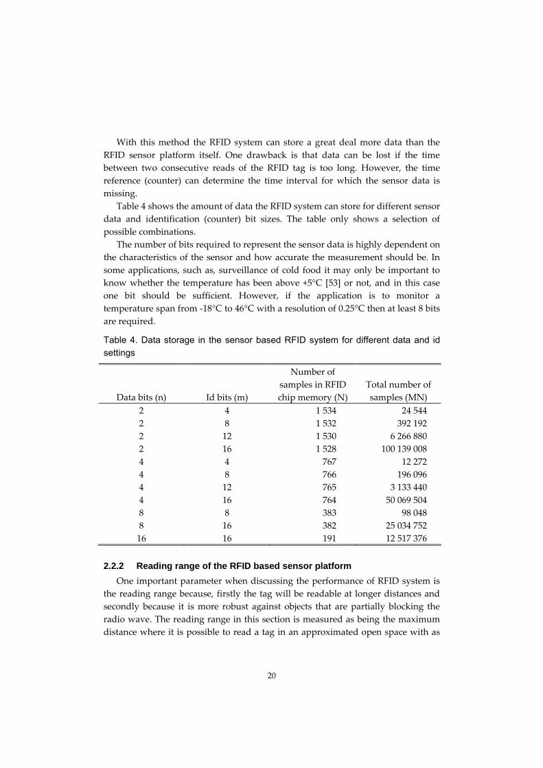
Table 4 shows the amount of data the RFID system can store for different sensor
data and identification (counter) bit sizes. The table only shows a selection of
possible combinations.
The number of bits required to represent the sensor data is highly dependent on
the characteristics of the sensor and how accurate the measurement should be. In
some applications, such as, surveillance of cold food it may only be important to
know whether the temperature has been above +5°C [53] or not, and in this case
one bit should be sufficient. However, if the application is to monitor a
temperature span from ‐18°C to 46°C with a resolution of 0.25°C then at least 8 bits
are required.
Table 4. Data storage in the sensor based RFID system for different data and id
settings
Data bits (n) Id bits (m)
Number of
samples in RFID
chip memory (N)
Total number of
samples (MN)
2 4 1 534 24 544
2 8 1 532 392 192
2 12 1 530 6 266 880
2 16 1 528 100 139 008
4 4 767 12 272
4 8 766 196 096
4 12 765 3 133 440
4 16 764 50 069 504
8 8 383 98 048
8 16 382 25 034 752
16 16 191 12 517 376
2.2.2 Reading range of the RFID based sensor platform
One important parameter when discussing the performance of RFID system is
the reading range because, firstly the tag will be readable at longer distances and
secondly because it is more robust against objects that are partially blocking the
radio wave. The reading range in this section is measured as being the maximum
distance where it is possible to read a tag in an approximated open space with as
20
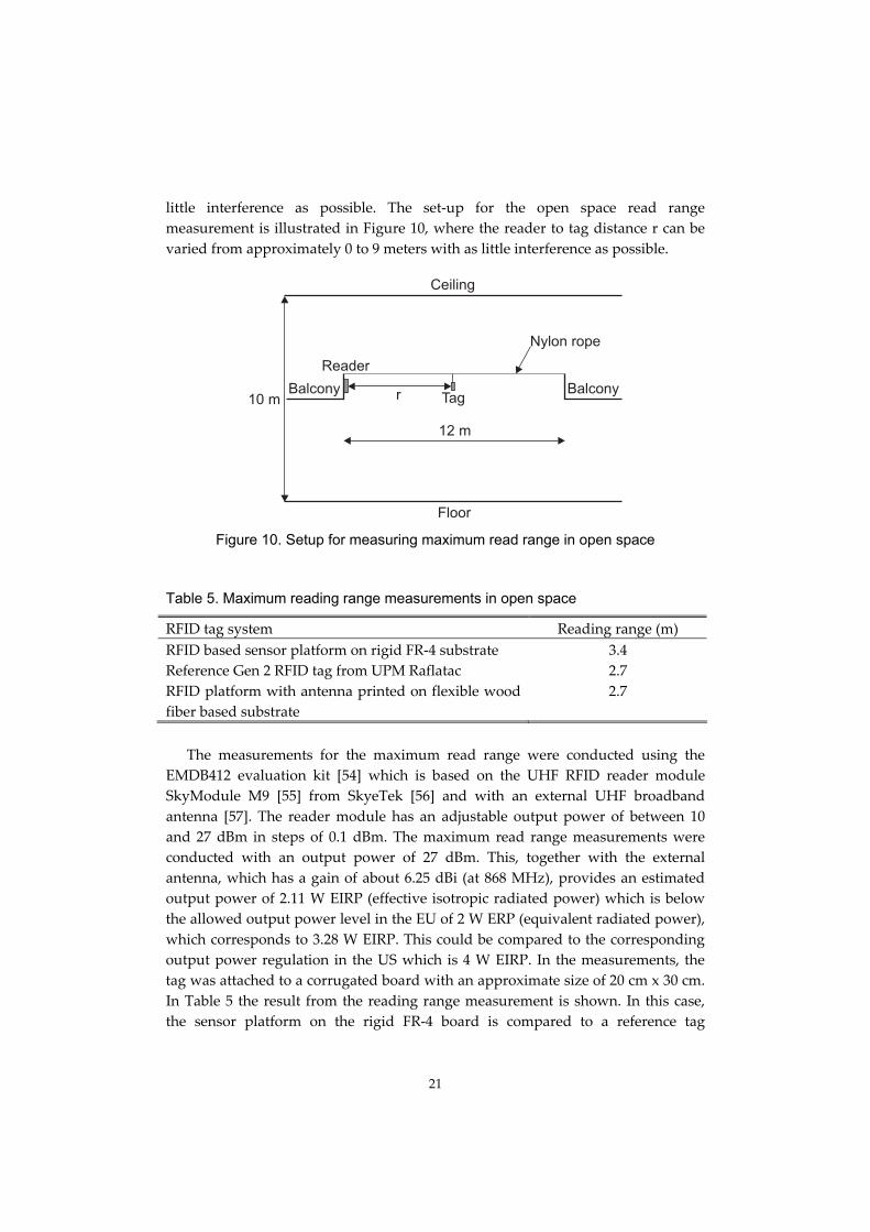
little interference as possible. The set‐up for the open space read range
measurement is illustrated in Figure 10, where the reader to tag distance r can be
varied from approximately 0 to 9 meters with as little interference as possible.
Ceiling
Floor
Balcony Balcony
Reader
Tagr10 m
12 m
Nylon rope
Figure 10. Setup for measuring maximum read range in open space
Table 5. Maximum reading range measurements in open space
RFID tag system Reading range (m)
RFID based sensor platform on rigid FR‐4 substrate 3.4
Reference Gen 2 RFID tag from UPM Raflatac 2.7
RFID platform with antenna printed on flexible wood
fiber based substrate
2.7
The measurements for the maximum read range were conducted using the
EMDB412 evaluation kit [54] which is based on the UHF RFID reader module
SkyModule M9 [55] from SkyeTek [56] and with an external UHF broadband
antenna [57]. The reader module has an adjustable output power of between 10
and 27 dBm in steps of 0.1 dBm. The maximum read range measurements were
conducted with an output power of 27 dBm. This, together with the external
antenna, which has a gain of about 6.25 dBi (at 868 MHz), provides an estimated
output power of 2.11 W EIRP (effective isotropic radiated power) which is below
the allowed output power level in the EU of 2 W ERP (equivalent radiated power),
which corresponds to 3.28 W EIRP. This could be compared to the corresponding
output power regulation in the US which is 4 W EIRP. In the measurements, the
tag was attached to a corrugated board with an approximate size of 20 cm x 30 cm.
In Table 5 the result from the reading range measurement is shown. In this case,
the sensor platform on the rigid FR‐4 board is compared to a reference tag
21

consisting of a Gen 2 tag from UPM Raflatac. In Table 5 the reading range is also
compared to a printed antenna. For the printed antenna the maximum reading
range was decreased to 2.7 m because the antenna layout was optimized for a rigid
FR‐4 substrate and also because of a higher sheet resistivity in the antenna
structure which leads to ohmic losses. The sheet resistivity of the printed antenna
was estimated to be approximately 120 mΩ/.
2.3 Applications for the RFID based sensor system
In this section the RFID based sensor platform is evaluated for three smart
packaging concepts for packaging surveillance applications.
2.3.1 Moisture content sensor solution
In this section the RFID based sensor platform is evaluated using a moisture
content sensor. The moisture content sensor solution is described in greater detail
in section 3.1. For this study three samples were produced by screen printing [58]
the two‐dimensional sensor structure (an example which can be seen in Figure 18)
with conductive silver ink (26‐8204) from Coates Screen [59] on a 100 μm thick
plastic film from MACtac [60]. These plastic films were then laminated onto wood
fibre based substrates. The substrate was a C‐flute corrugated board made out of
testliner [61] where the liner and the fluting had a base weight of 140 g/m2 and a
total thickness of 4 mm. The two‐dimensional conductive structure had an
electrode width of 4 mm and an electrode spacing of 1.2 mm and had a total size of
40x53 mm in a rectangular shape. The sensors were preconditioned at 20% relative
humidity and then exposed and logged at the following relative humidity levels:
30%, 50%, 70%, 85% and back to 70% at a constant temperature of 23°C. All the
measurements were made at equilibrium condition, which means that the samples
were exposed to the corresponding relative humidity level for 24 hours. The
moisture content in the wood fibre based substrates was measured using a HB45
halogen moisture analyser from Mettler Toledo [62]. The moisture content sensor is
a capacitive sensor which is read by charging the sensor to a fixed potential and
then measuring the discharge time. The readout solution is described in greater
detail in section 3.1.
In the evaluation of the moisture content sensor application, eight bits are used
for the sensor data values and for the identification number. This determined that
the RFID chip can store 383 data values while the whole system can store a total of
98048 sensor values as seen in Table 4. The moisture content changes in wood fibre
based materials is a rather slow process so a fast sampling rate is not necessary. A
sampling time of between 10 and 30 minutes between each sample is sufficient.
Figure 11 shows how long it takes to fill the RFID chip and the whole system,
respectively, for different sampling rates. As can be seen in Figure 11 if the system
22

has a sampling rate of 0.556e‐3 Hz, which corresponds to 30 minutes between
samples, the RFID chip can store sensor values for almost 8 days before the
memory is full, and the whole system can store data for 5.5 years.
The battery lifetime for the moisture content application greatly depends on the
sampling rate and the energy capacity of the battery. In Table 6 the current
consumption of the evaluated moisture content sensor system is presented. Here,
the different modes are shown together with the length of time that the system is in
the particular mode.
10−4
10−3
10−2
10−1
100
100
10−2
102
104
106
Sample rate (Hz)
Tim
e (h
)
RFID chipSensor system
Figure 11. The total amount of time to fill the RFID chip memory and the entire RFID sensor system respectively as a function of the sampling rate for the moisture
content sensor application
Table 6. Power consumption for the moisture content sensor application
Mode Current (μA) Time (ms)
Sleep 0.7 *
Sensor charge 500 1
Sensor discharge 1840 0.2
Data handling 500 5.4
SPI write sensor data 500 2**
SPI wait 7.8 20**
* Depends on the sampling rate
** Data storing (SPI write and SPI wait) is only active when 16 bit (word) of sensor
data is available. For a setup with 8 sensor bits, 2 sensor values (16 bits) are
needed before the data is stored in the RFID chip
23

3.5
10−4
10−3
10−2
10−1
100
0.5
1
1.5
2
2.5
3
Sample rate (Hz)
Bat
tery
life
time
(yea
rs)
33 mAh10 mAh
Figure 12. The estimated battery lifetime of the moisture content sensor setup as a
function of the sampling rate for different battery energy capacities with a self-discharge of 10% per year
90
4 6 8 10 12 14 160
10
20
30
40
50
60
70
80
Moisture content (%)
Nor
mal
ized
dis
char
ge ti
me
(µs)
Figure 13. Normalized discharge time as a function of the moisture content in the
substrates for three moisture content sensors
In Figure 12 the estimated battery lifetime of the moisture content sensor is
shown for two different battery energy capacities, a self‐discharge of 10% per year
for the battery has been included in the calculation. As can be seen in Figure 12 for
24

a battery with an energy capacity of 33 mAh, the sensor platform should have an
estimated battery lifetime of 3.4 years with a sample rate below 0.1 Hz.
In Figure 13 the normalized discharge time is plotted as a function of the
moisture content. The discharge time is normalized against the response when no
sensor is connected to the microcontroller. As can be seen, the sensors in the
particular set‐up are unable to distinguish between moisture content levels below
six percent. However, this sensor is designed to be used at higher moisture content
levels, which correspond to 50% relative humidity and above.
Table 7. Temperature measurements on the moisture content sensor at 70% relative humidity (mean of 3 sensors)
Temperature (°C) Moisture content (%) Discharge time (μs)
18 11.01 27.0
23 10.74 26.0
30 10.50 25.5
In Table 7 the temperature dependency of the sensor and the moisture content
of the substrate are shown for a constant relative humidity of 70%. As can be seen
in the measurements, the moisture content is decreasing with a higher
temperature, which corresponds to earlier observations [34]. However, when the
temperature increases the amount of water in the air increases for a constant
relative humidity level, for example, when the temperature reduces from 18°C to
30°C the vapour density almost doubles [63]. The decrease for the moisture content
is because it is the chemical potential that determines the quantity of moisture or
water vapour. As the temperature of a two phase system is increased, the
concentration in the vapour phase increases at the expense of that in the
condensed/adsorbed phase but the chemical potentials remain the same between
the two phases at equilibrium [64]. Large variations in temperature could lead to
false moisture content measurements. However, the sensor set‐up has a built‐in
temperature sensor which, together with the moisture content sensor, could give
both a more accurate moisture response and also the possibility to estimate the
relative humidity.
As can be seen in the results in Figure 13 it is possible to reduce the number of
sensor levels to, for example, seven (instead of 256) and still obtain a rather good
estimation of the moisture content level. This should decrease the number of
sensor data bits (n) to 3 which should increase the number of sensor bits that could
be stored in the RFID chip to 1021, if nine id bits (m) are used, and thus greatly
increase the memory lifetime of the sensor system.
25
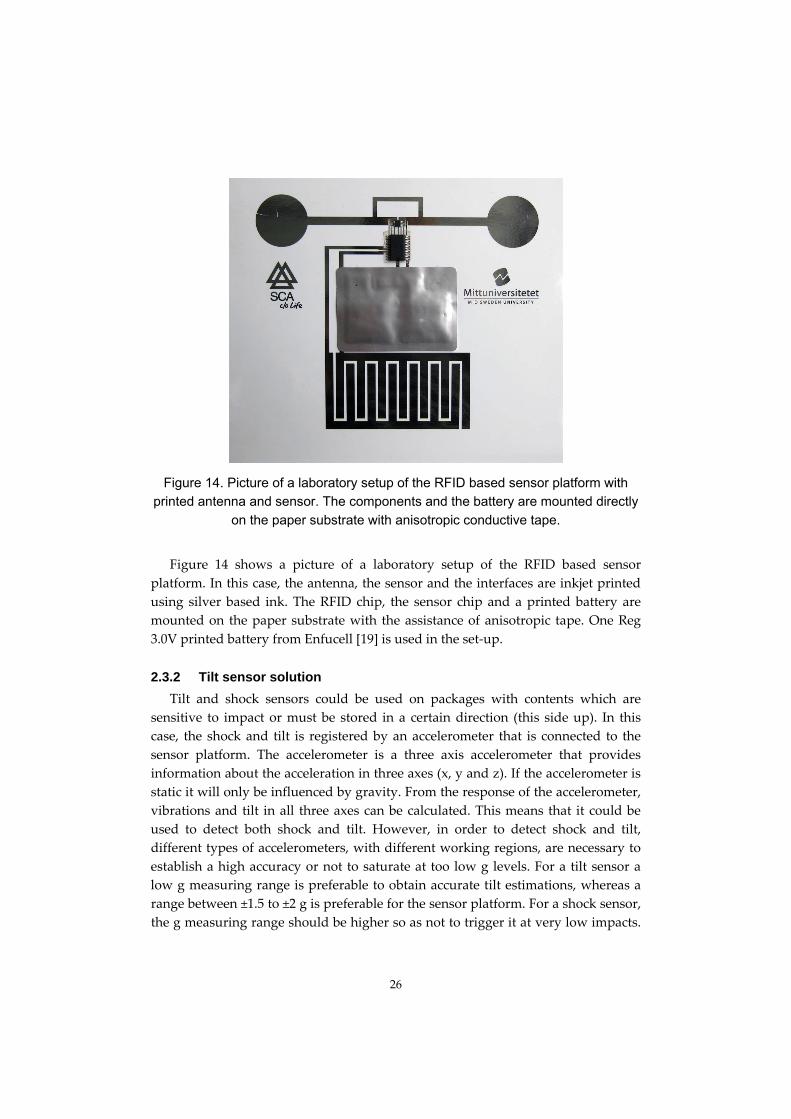
Figure 14. Picture of a laboratory setup of the RFID based sensor platform with printed antenna and sensor. The components and the battery are mounted directly
on the paper substrate with anisotropic conductive tape.
Figure 14 shows a picture of a laboratory setup of the RFID based sensor
platform. In this case, the antenna, the sensor and the interfaces are inkjet printed
using silver based ink. The RFID chip, the sensor chip and a printed battery are
mounted on the paper substrate with the assistance of anisotropic tape. One Reg
3.0V printed battery from Enfucell [19] is used in the set‐up.
2.3.2 Tilt sensor solution
Tilt and shock sensors could be used on packages with contents which are
sensitive to impact or must be stored in a certain direction (this side up). In this
case, the shock and tilt is registered by an accelerometer that is connected to the
sensor platform. The accelerometer is a three axis accelerometer that provides
information about the acceleration in three axes (x, y and z). If the accelerometer is
static it will only be influenced by gravity. From the response of the accelerometer,
vibrations and tilt in all three axes can be calculated. This means that it could be
used to detect both shock and tilt. However, in order to detect shock and tilt,
different types of accelerometers, with different working regions, are necessary to
establish a high accuracy or not to saturate at too low g levels. For a tilt sensor a
low g measuring range is preferable to obtain accurate tilt estimations, whereas a
range between ±1.5 to ±2 g is preferable for the sensor platform. For a shock sensor,
the g measuring range should be higher so as not to trigger it at very low impacts.
26

The commercially available shock indicators, for example from ShockWatch, are
designed to have a triggering level from 10 g to 100 g [65]. Thus, for the shock
sensor application that should work in the same region as the indicators, the
accelerometer should have a measuring range of at least 100 g.
In this case, a low g accelerometer from Freescale is used for the tilt sensor
application. The MMA7260Q [66] is a three axis accelerometer with three analogue
outputs (x, y and z). The accelerometer has a selectable measuring range with the
following ranges, ±1.5, ±2, ±4 and ±6g. In this set‐up the analogue outputs is
connected to three ADC channels on the microcontroller in order to measure the
acceleration in all three axes.
For commercially available tilt indicators, a few different types exists, for
example, TiltWatch XTR [67] that indicates if the tilt has been more than 80° or the
TiltWatch Plus [67] that indicates angles with an increment of 10° from a 30° tilt
and above. The tilt sensor described is intended to be used in, for example, tilt
detection in packages. For a performance test of the tilt sensor set‐up a tilt detector
is proposed that detects tilt angles from 0° to 360° in increments of 45°. For this
specific application set‐up, four bits are used to represent the tilt angle and eight
bits are used for the identification number. Thus, the RFID chip can store a total of
766 sensor values while the entire sensor system can store a total of 196096 sensor
values as seen in Table 4.
10−3
10−2
10−1
100
10−2
100
102
104
106
RFID chipSensor system
Sample rate (Hz)
Tim
e (h
)
Figure 15. The total amount of time to fill the RFID chip memory and the entire RFID sensor system respectively as a function of the sampling rate for the tilt
sensor application
27
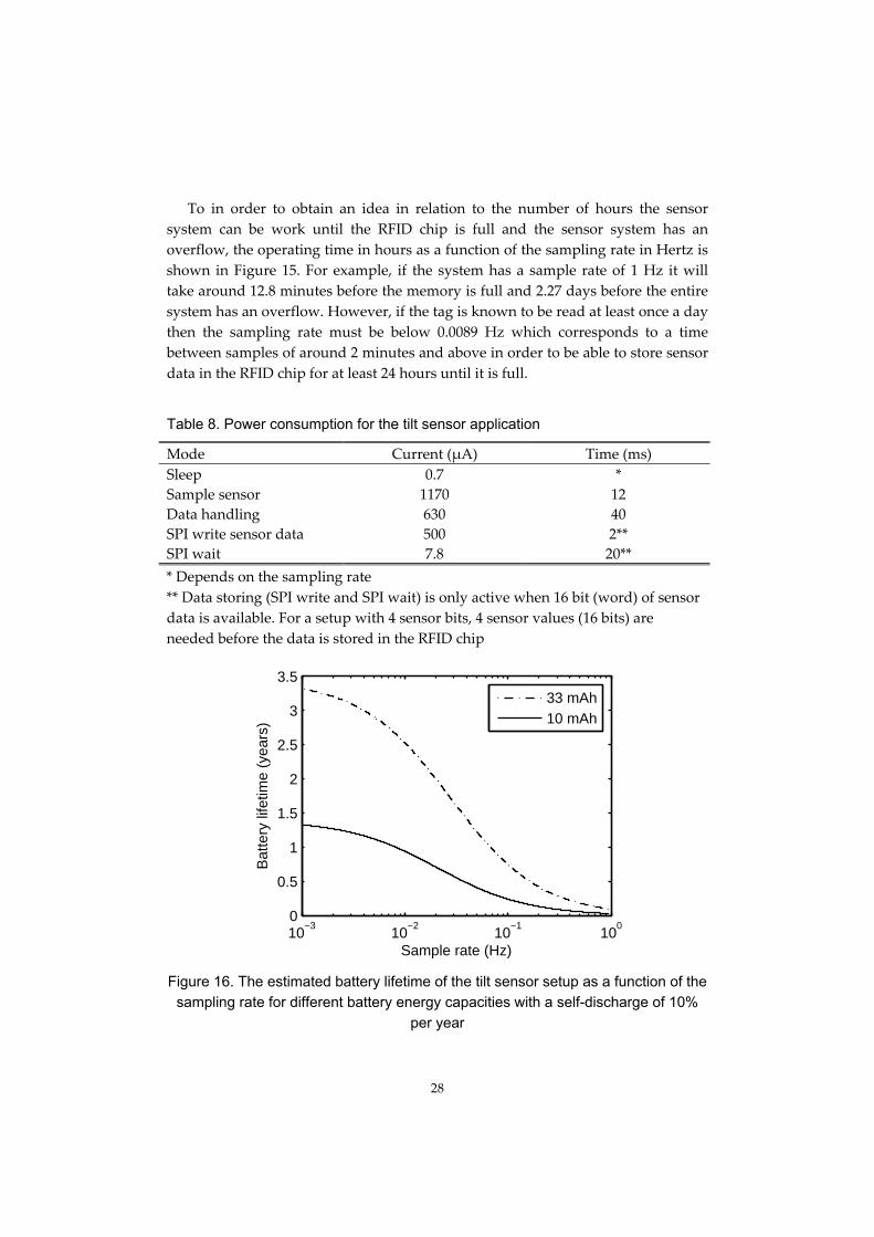
To in order to obtain an idea in relation to the number of hours the sensor
system can be work until the RFID chip is full and the sensor system has an
overflow, the operating time in hours as a function of the sampling rate in Hertz is
shown in Figure 15. For example, if the system has a sample rate of 1 Hz it will
take around 12.8 minutes before the memory is full and 2.27 days before the entire
system has an overflow. However, if the tag is known to be read at least once a day
then the sampling rate must be below 0.0089 Hz which corresponds to a time
between samples of around 2 minutes and above in order to be able to store sensor
data in the RFID chip for at least 24 hours until it is full.
Table 8. Power consumption for the tilt sensor application
Mode Current (μA) Time (ms)
Sleep 0.7 *
Sample sensor 1170 12
Data handling 630 40
SPI write sensor data 500 2**
SPI wait 7.8 20**
* Depends on the sampling rate
** Data storing (SPI write and SPI wait) is only active when 16 bit (word) of sensor
data is available. For a setup with 4 sensor bits, 4 sensor values (16 bits) are
needed before the data is stored in the RFID chip
3.5
10−3
10−2
10−1
100
0
0.5
1
1.5
2
2.5
3
Sample rate (Hz)
Bat
tery
life
time
(yea
rs)
33 mAh10 mAh
Figure 16. The estimated battery lifetime of the tilt sensor setup as a function of the sampling rate for different battery energy capacities with a self-discharge of 10%
per year
28
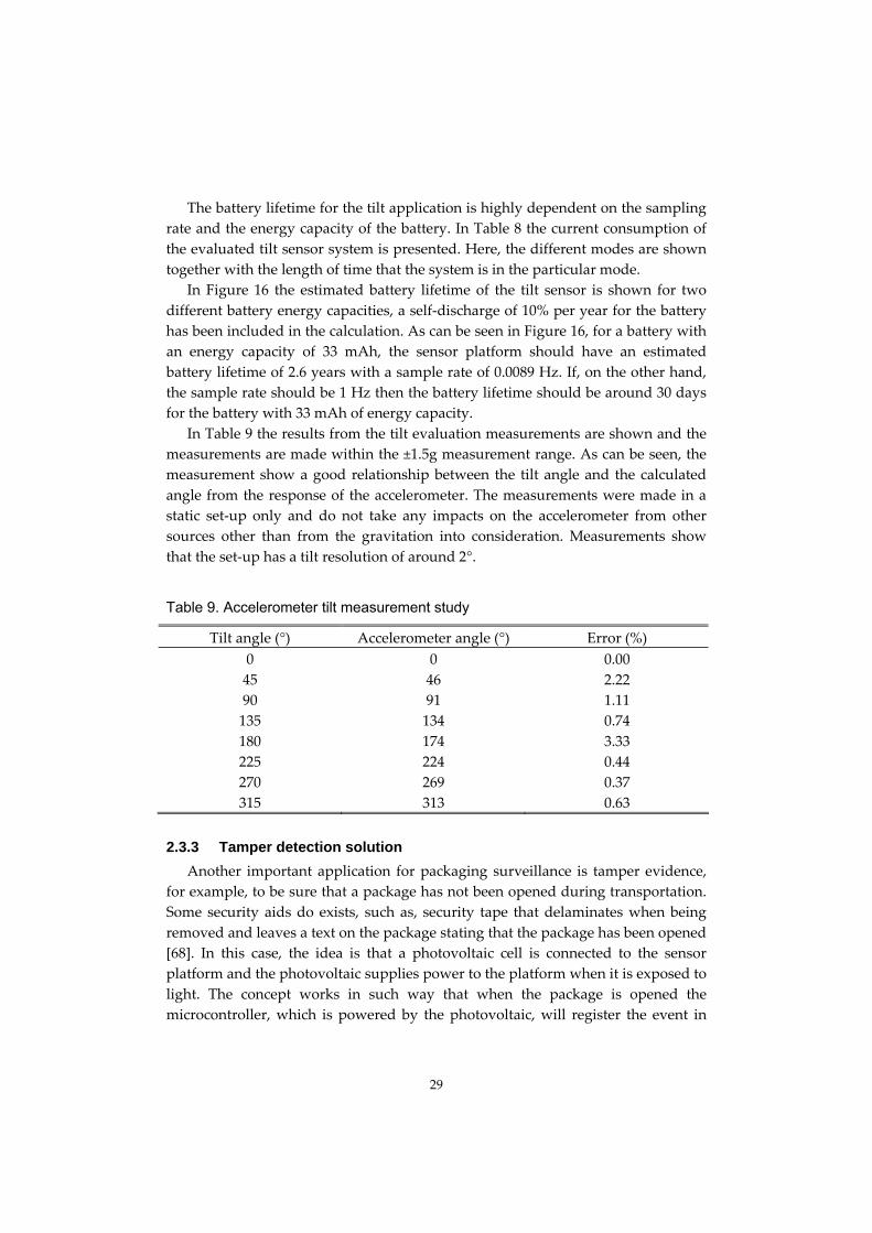
The battery lifetime for the tilt application is highly dependent on the sampling
rate and the energy capacity of the battery. In Table 8 the current consumption of
the evaluated tilt sensor system is presented. Here, the different modes are shown
together with the length of time that the system is in the particular mode.
In Figure 16 the estimated battery lifetime of the tilt sensor is shown for two
different battery energy capacities, a self‐discharge of 10% per year for the battery
has been included in the calculation. As can be seen in Figure 16, for a battery with
an energy capacity of 33 mAh, the sensor platform should have an estimated
battery lifetime of 2.6 years with a sample rate of 0.0089 Hz. If, on the other hand,
the sample rate should be 1 Hz then the battery lifetime should be around 30 days
for the battery with 33 mAh of energy capacity.
In Table 9 the results from the tilt evaluation measurements are shown and the
measurements are made within the ±1.5g measurement range. As can be seen, the
measurement show a good relationship between the tilt angle and the calculated
angle from the response of the accelerometer. The measurements were made in a
static set‐up only and do not take any impacts on the accelerometer from other
sources other than from the gravitation into consideration. Measurements show
that the set‐up has a tilt resolution of around 2°.
Table 9. Accelerometer tilt measurement study
Tilt angle (°) Accelerometer angle (°) Error (%)
0 0 0.00
45 46 2.22
90 91 1.11
135 134 0.74
180 174 3.33
225 224 0.44
270 269 0.37
315 313 0.63
2.3.3 Tamper detection solution
Another important application for packaging surveillance is tamper evidence,
for example, to be sure that a package has not been opened during transportation.
Some security aids do exists, such as, security tape that delaminates when being
removed and leaves a text on the package stating that the package has been opened
[68]. In this case, the idea is that a photovoltaic cell is connected to the sensor
platform and the photovoltaic supplies power to the platform when it is exposed to
light. The concept works in such way that when the package is opened the
microcontroller, which is powered by the photovoltaic, will register the event in
29

the RFID chip. From the registered events it is possible to determine how many
times and for how long time the package has been opened.
In the evaluated set‐up the XOB17‐04x3 XOLAR SolarBITs [69] from IXYS
Corporation [70], which provide a maximum of 1.53 V, have been used. In the
measurements two photovoltaic cells are required in order to provide above 1.8 V
to the platform which is necessary to power up the microcontroller and to store the
event in the RFID chip. The photovoltaic cells have an estimated active area of 1.08
cm2 each.
In Figure 17 the result from the measurements on the photovoltaic cells are
shown for different loads. In the measurements, fluorescent lamps are used, which
are commonly used in warehouses. The measurements show that the incident light
from the fluorescent lamps must have intensity above 500 lux to provide sufficient
voltage to power up the microcontroller and sufficient energy to be able to perform
a write instruction to the RFID chip at the lowest microcontroller oscillator
frequency. This is based on a voltage of 1.86 V and a 50 kΩ resistor which
corresponds to a current consumption of 37 μA. The intensity necessary to power
up the platform could of course be reduced by increasing the active area of the
photovoltaic cells.
0 200 400 600 800 1000 1200 14000
0.5
1
1.5
2
3
2.5
Intensity (lux)
Out
put v
olta
ge (
V)
Figure 17. Output voltage from the photovoltaic cells as a function of incident light
intensity for different loads. Solid line no external resistor, dash-dotted line R = 1130kΩ, dash-dash line R = 560kΩ, dotted line R = 100kΩ, () R = 50kΩ
and (◊) R = 10kΩ
30

Table 10. Photovoltaic cells measured under incandescent light bulb with a light intensity of 610 lux
Load Output voltage (V)
No external resistor 3.070
1 130kΩ 3.063
570kΩ 3.072
100kΩ 3.041
50kΩ 3.017
10kΩ 2.666
As can be seen in Table 10 if an ordinary incandescent light bulb is used instead
of a fluorescent lamp, the output voltage from the photovoltaic cells is much
higher, for example, 610 lux can power a 10 kΩ load to 2.7 V which corresponds to
a current of 0.27 mA. The high increase in energy when using an incandescent light
bulb, instead of a fluorescent light, is highly likely to be because an incandescent
light bulb has a smoother intensity curve with a higher energy over the whole
visible wavelength spectra.
As seen in the results, the sensor platform together with the photovoltaic cells
can be used to create a tamper evidence solution for packages that shows whether
the package has been opened. The technique, naturally, has some disadvantages,
such as an opening event can only be detected if the light intensity is sufficient to
power up the microcontroller from the photovoltaic cells. However, there is the
possibility to use the photovoltaic cells as a trigger for a system powered by a
battery. Then, a much lower light intensity is required in order to detect the event.
2.4 Wireless sensor platform comparison
In this section the proposed RFID based sensor platform is compared to other
wireless sensor platform solutions. The platforms are both based on RFID
technology and on other types of communication technologies.
2.4.1 Wi-Fi technology
Folea et al. [71] have presented an ultra low power Wi‐Fi sensor platform which
is based on the IEEE 802.11b standard operating at 2.4 GHz. The sensor platform
has a reading range of up to 50 m in an indoor environment. The IEEE 802.11b
standard also makes it feasible to work with a very high data rate of up to 11
Mbps. One downside associated with the Wi‐Fi solution is that it is an active tag,
which means that the sensor platform requires power from a battery, or similar, to
be able to transmit the sensor data to the reader (or access point). The sensor
platform consumes 700 mA for 1 – 5 ms while it transmits the sensor data.
31

However a sensor platform is at sleep for the majority of the time and during sleep
it consumes between 4 and 10 μA. The power consumptions above are based on a
3V power supply.
2.4.2 Infrared technology
Mattoli et al. [72] have presented a flexible data logger based on the IrDA
(infrared) communication standard. The sensor platform has a reading range of 10
cm and because it is based on infrared communication the tag must be in line of
sight of the reader. The communication between the tag and the reader occur at a
speed of 19.2 kbps. The infrared sensor platform is, as the Wi‐Fi, based on an active
sensor platform, which means that the transmitter must have energy from an
internal power source, for example a battery. The infrared sensor platform
consumes 1.8 mA (3 V) for 5.5 ms while transmitting the sensor data. As with all
sensor platforms the power consumption during sleep is very important for a long
battery lifetime of the sensor platform. The infrared sensor platform has a sleep
power consumption of 1.3 μA (3 V).
2.4.3 Impulse Ultra Wideband (I-UWB)
The impulse ultra wideband (I‐UWB) technology can be seen as a hybrid
version of the ordinary passive UHF RFID technology. The I‐UWB technique
presented by Baghaei‐Nejad et al. [73] uses an ordinary EPC class 1 protocol for the
downlink communication (reader to tag) and for the remote powering of the tag.
However, in the uplink communication (tag to reader), it uses short pulses for data
transmission which provides a higher data rate. According to Baghaei‐Nejad et al.
[73] the I‐UWB technology can reach an uplink data rate of up to 10 Mbps. Since
the majority of the data in a sensor platform is sent from the tag to the reader, the
technology might be a suitable candidate for a sensor platform. The I‐UWB
technology is, however, not a standard communication protocol, which means that
it will not work with the existing Gen 2 readers and infrastructure. The platform
has an input sensitivity of ‐18.5 dBm which gives an estimated reading range of
13.9 m considering 4W EIRP and 0 dB gain of the antenna. The low input
sensitivity and the long reading range is, according to Baghaei‐Nejad et al. [73],
mainly due to the use of a voltage sensor which reduces the power consumption
during the harvesting time. The voltage sensor activates the tag only when the
storage capacitor reaches a certain voltage (2.75V) and when the voltage drops
below 1.9V the operation is stopped and the storage capacitor is recharged [73].
The tag consumes 51 μA (1.8V) at 10 MHz pulse rate while transmitting data to the
reader. One downside associated with the I‐UWB tag solution is that it is remotely
powered which means that the sensor can only store sensor data when the tag is
within the reading range of the reader.
32
2.4.4 Passive RFID solution
A few sensor enabled passive RFID tags exists [48‐50, 74]. Passive RFID tags use
the energy from the reader to power the tag. This means that the passive RFID
technology has an almost unlimited lifetime. However, it also means that they can
only store sensor data when the tag is powered by the reader. An ordinary passive
RFID tag has a return link (tag to reader) data rate up to 640 kbps and a reading
range up to 4.5 m (4 W EIRP) [50].
2.4.5 Wirelessly-charged RFID
A wirelessly‐charged RFID tag basically means a semi‐passive tag without
batteries. Instead, the tag harvests the energy it acquires from the reader and stores
it in a capacitor to be used when the tag is away from the reader. Yeager et al. [51]
have presented a wirelessly‐charged UHF tag for sensor data collection. The tag
uses the Gen 2 standard for communication. The presented RFID tag has a reading
range of 4.5 m. However, they state that the tag can be charged at a distance of up
to 10 m from the reader. The tag uses the Gen 2 standard and has a return link (tag
to reader) data rate of up to 640 kbps. The tag is a semi‐passive tag which means
that the tag works in a similar manner to a passive tag while communicating with
the reader, and does not consume any (or very little) of the stored energy when
communicating. The sensor platform has a sleep power consumption of 1.8 μA
operating at 1.8V. The tag is designed so that when the tag is within the vicinity of
the reader, it charges the capacitor and when no reader is in the vicinity the tag
uses the stored energy to read out the sensor and store the data in the memory. The
tag presented by Yeager et al. [51] is designed to work for 24 hours when the
capacitor is fully charged. The charge time for the tag is dependent on the distance
to the reader, according to Yeager et al. [51] the predicted charge time for 1 m
distance is about 20 minutes.
2.4.6 Summary of comparison between different wireless sensor platforms
The different wireless sensor solutions presented in this section all have some
advantages and disadvantages. However, it is highly unlikely that some of them
will be used for packaging surveillance in the supply chain. In Table 11 the
different communication technologies are listed with some notes stating how
suitable they are for packaging surveillance applications in the supply chain.
33

Table 11. Comparison between different wireless sensor solutions
Technology Notes
WiFi WiFi is an active radio tag and is not suitable to be used
the supply chain. The technology is not compatible with
the current standard for item level tagging.
IrDA IrDA must have line of sight in order to be read which
make it not suitable to be used in the supply chain.
I‐UWB I‐UWB is an interesting technology which allows high
data rate for a short period of time. However it is not
fully developed for sensing functionality and it is not
compatible with the Gen 2 standard.
Passive RFID Passive RFID is not possible to use as a logger because it
needs energy from the reader in order to gather sensor
data.
Wirelessly‐charged
RFID
Wirelessly‐charged RFID is an interesting solution in
sensor data logging. However the short operation time
and long charging time makes it not suitable to be used
in the supply chain. The technology could, however,
together with other energy harvesting solutions be very
interesting.
Two‐chip semi‐
passive RFID*
The two‐chip solution presented in this study could very
well be used in data logging in the supply chain, with a
long lifetime and the possibility to be tailored to work
with many different types of sensors.
* This work
34

3 LOW COST MOISTURE SENSORS
The introduction of the Gen 2 standard as a replacement for traditional bar‐
codes in packaging has opened up new markets for intelligent packaging. Not only
will it be possible to read many packages simultaneously, it will also be possible to
incorporate different types of sensors into the packages. It is of significant interest
to be able to track the condition of a package during its transportation through the
supply chain. This makes it possible to guarantee that the package has not been
exposed to the wrong conditions or climate, for example, to check that frozen food
has not been exposed to temperatures that are too high.
Today around 40% of all packages used are manufactured of wood fibres [28]
and moisture has a large influence on the board strength of wood fibre materials.
Thus, measuring the moisture could provide vital information with regards to
dimensioning the package in the right way. It is known that the strength of a wood
fibre based package is considerably reduced when exposed to high relative
humidity levels [33]. For example Benson [34] shows that if the relative humidity is
changed from 50% to 90% the strength of the wood fibre based paper is reduced to
half its original value. Since wood fibre based paper is a hygroscopic material it
absorbs and desorbs moisture according to the relative humidity in its
surroundings. However, the moisture content (the amount of water in the paper) is
not only determined by the present relative humidity level but rather depends on
the history of the relative humidity changes in the surroundings [33]. When many
of the paper properties are plotted against the relative humidity they display
hysteresis phenomena [75]. However, these hysteresis phenomena can be removed
if the paper properties are instead plotted against the moisture content of the
paper. One of the most critical moisture situations with reference to wood fibre
based packages involves the relative humidity cycles between dry conditions and
high moisture levels when the package is under a constant load [76]. This situation
is significantly more crucial than for the case in which the package is exposed to a
constant high humidity level. Thus, moisture sensing in packages and moisture
logging is very important in order to determine the condition of the package.
In this section five different types of moisture sensors are presented. The first
involves a moisture content sensor for wood fibre based substrates based on a
capacitive measuring technique, the second is a relative humidity sensor for high
humidity levels based on a resistive measuring technique. The third is an action
activated moisture sensor that is producing a voltage signal when exposed to
moisture. The fourth is a remote moisture sensor utilizing ordinary passive or
semi‐passive RFID tags in order to measure the moisture. Finally there are two
types of moisture sensors that are utilizing silver nano‐particles as a moisture
sensing substance.
35

36
The first three and the fifth sensor solutions, which are printed sensors, are
designed to be easily integrated into the RFID based sensor platform described in
section 2 whereas the fourth, the remote moisture sensor solution, utilizes ordinary
RFID tags for moisture detection. The concept of dual measurements in moisture
sensor could be integrated into the RFID based sensor system for higher accuracy.
3.1 Moisture content sensor for wood fibre based substrates
In this section a moisture content sensor for wood fibre based substrates is
presented, and this is the same sensor as was presented previously in section 2.3.1.
Typical applications are moisture detection in smart packages and in building
materials. The sensor is based on a two‐dimensional conductive structure and
could be shaped for example as seen in Figure 18.
Figure 18. Example of a layout of a sensor structure shaped as a circle
R2
C2 C2
C1
Conductive
Dielectric
Substrate
applying the structure on a wood fibre based substrate with an insulation or
Figure 19. A cross section of the moisture content sensor for wood fibre based substrates
By measuring the capacitance between the two electrodes of the two‐
dimensional structure the moisture level in the surroundings can be detected. By

dielectric layer in between, as seen in Figure 19, the moisture level in the substrate
can be measured.
There are different ways of measuring capacitances. In this case, in packaging
surveillance, the intention is to allow simple integration in an all digital circuit
solution and therefore the capacitance is measured by charging the sensor to a
fixed potential and then measuring the discharged time over a resistor to a
predetermined level. The discharge time is proportional to the capacitance value of
the sensor. In equation (5) the discharge equation of a capacitor in series with a
resistor can be seen. In Figure 20 typical discharge curves from two capacitors, one
of 10 pF and one of 20 pF over a 100kΩ resistor can be seen. The marked values are
the time taken to discharge the capacitors to 37% of the initial value. A discharge
time, which is twice as long, can be observed for the larger capacitor.
tRCEetu1
)(
(5)
here E is the initial voltage, R and C are the resistor and capacitor values
res
w
pectively and t is the time from the start of the discharge.
1
0 0.2 0.4 0.6 0.8 1
x 10−5
0
0.2
0.4
0.6
10pF20pF0.8
Time (s)
Nor
mal
ized
vol
tage
(d.
u.)
Figure 20. Typical discharge curves from two capacitors over a 100kΩ resistor. The
hen the moisture content in the wood fibre based substrates changes, its
con
dashed lines mark the discharge time to 37% of the initial voltage value
W
ductivity will also change, as seen in earlier observations [29‐30]. As the
37
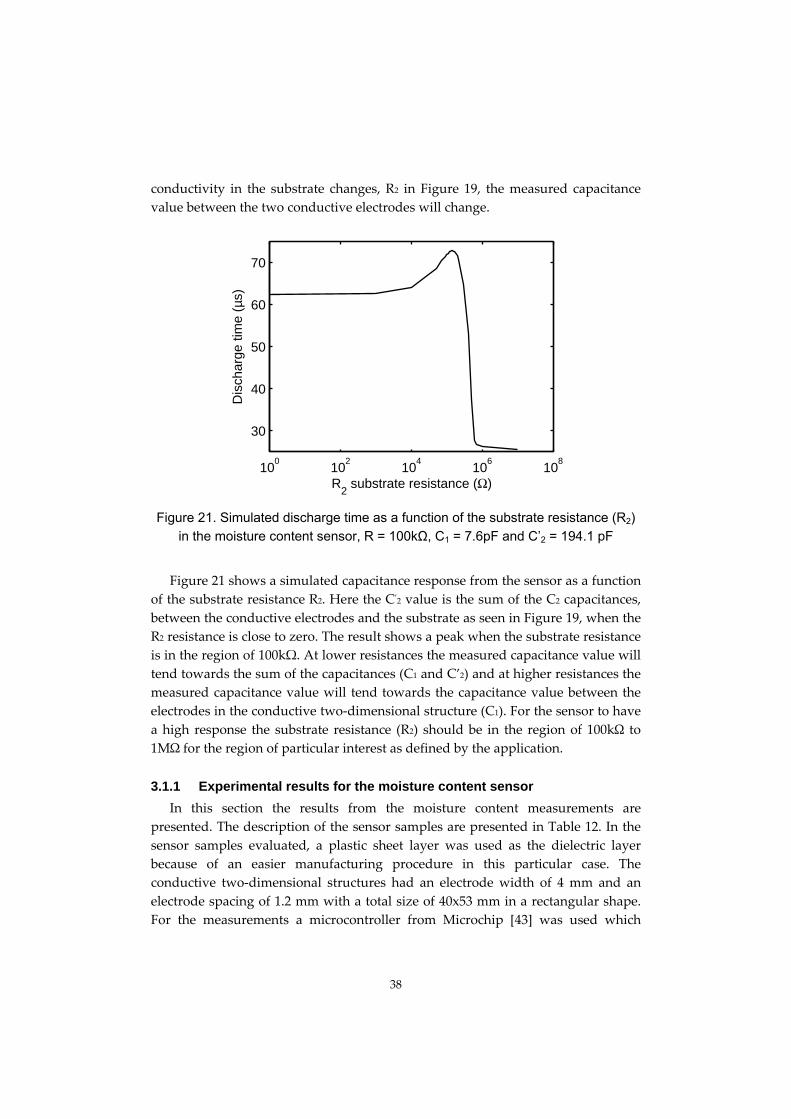
conductivity in the substrate changes, R2 in Figure 19, the measured capacitance
value between the two conductive electrodes will change.
100
102
104
106
108
30
40
50
60
70
Dis
char
ge ti
me
(µs)
R2 substrate resistance (Ω)
Figure 21. Simulated discharge time as a function of the substrate resistance (R2) in the moisture content sensor, R = 100kΩ, C1 = 7.6pF and C’2 = 194.1 pF
Figure 21 shows a simulated capacitance response from the sensor as a function
of the substrate resistance R2. Here the C’2 value is the sum of the C2 capacitances,
between the conductive electrodes and the substrate as seen in Figure 19, when the
R2 resistance is close to zero. The result shows a peak when the substrate resistance
is in the region of 100kΩ. At lower resistances the measured capacitance value will
tend towards the sum of the capacitances (C1 and C’2) and at higher resistances the
measured capacitance value will tend towards the capacitance value between the
electrodes in the conductive two‐dimensional structure (C1). For the sensor to have
a high response the substrate resistance (R2) should be in the region of 100kΩ to 1MΩ for the region of particular interest as defined by the application.
3.1.1 Experimental results for the moisture content sensor
In this section the results from the moisture content measurements are
presented. The description of the sensor samples are presented in Table 12. In the
sensor samples evaluated, a plastic sheet layer was used as the dielectric layer
because of an easier manufacturing procedure in this particular case. The
conductive two‐dimensional structures had an electrode width of 4 mm and an
electrode spacing of 1.2 mm with a total size of 40x53 mm in a rectangular shape.
For the measurements a microcontroller from Microchip [43] was used which
38

charges the sensor to a fixed potential, in this case 5V, and measures the discharge
time to a low TTL level. In the evaluated sensor set‐up, the charge time was set to 1
millisecond. The oscillator frequency of the microcontroller was 16 MHz and the
discharge time was measured with a 16 bit counter which provides a time
resolution of 0.25 μs and a maximum measurable discharge time of 16.4
milliseconds. The measurements were made in a climate chamber where the
humidity and the temperature could be held at a predetermined constant level.
Moisture content measurements are a slow process because it takes a particular
time for the substrate to absorb or desorb the moisture in the surroundings [33]. All
the measurements in this study were made at equilibrium conditions, i.e. the
substrates were exposed to a given relative humidity level for at least 24 hours [33].
Table 12. Description of the moisture content sensor samples evaluated
Sample Substrate Dielectric Conductive
MC1 Single wall C‐flute [77]
corrugated board made
out of kraftliner [61]
100 μm thick
plastic film from
MACtac [60]
Screen printed [58]
conductive silver ink
(26‐8204) from Coates
Screen [59]
MC2 Single wall C‐flute [77]
corrugated board made
out of testliner [61]
100 μm thick
plastic film from
MACtac [60]
Screen printed [58]
conductive silver ink
(26‐8204) from Coates
Screen [59]
In Figure 22 the discharge time of the sensor samples MC1 and MC2, described
in Table 12, are presented as a function of the relative humidity in the range from
50% to 90%. As can be seen the sensor samples show a hysteresis effect, this is
because wood fibre based material is hygroscopic [33]. In Figure 23 the discharge
time for the sensor samples is, instead, plotted as a function of the moisture content
in the wood fibre based substrate. The result shows that there is a good correlation
between the sensor output and the moisture content in the substrate, both in the
absorption and desorption stage.
39
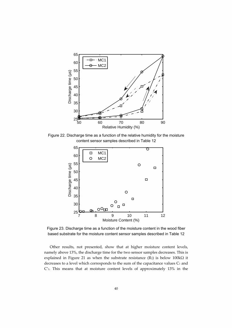
50 60 70 80 9025
30
35
40
45
50
55
65
60
Relative Humidity (%)
Dis
char
ge ti
me
(µs)
MC1MC2
Figure 22. Discharge time as a function of the relative humidity for the moisture content sensor samples described in Table 12
65
7 8 9 10 11 1225
30
35
40
45
50
55
MC1
60MC2
Moisture Content (%)
Dis
char
ge ti
me
(µs)
Figure 23. Discharge time as a function of the moisture content in the wood fiber based substrate for the moisture content sensor samples described in Table 12
Other results, not presented, show that at higher moisture content levels,
namely above 13%, the discharge time for the two sensor samples decreases. This is
explained in Figure 21 as when the substrate resistance (R2) is below 100kΩ it
decreases to a level which corresponds to the sum of the capacitance values C1 and
C’2. This means that at moisture content levels of approximately 13% in the
40

samples evaluated the substrate resistance is around 100kΩ and at even higher
moisture content levels the substrate resistance will decrease further [29‐30] and
thus the measured capacitance value will be reduced as seen in Figure 21. As this
could, unfortunately, give false readings from the sensors, it is preferable to
manufacture the sensor in such way that the substrate resistance (R2) should be in
the region of 100kΩ to 1MΩ for the region of particular interest as defined by the
application.
A study to determine whether the temperature had any influence on the
moisture content sensor samples was conducted. These measurements were made
in a climate chamber where the relative humidity was held at a constant level of
50% and the temperature was altered from 18°C up to 30°C. The results displayed
in Table 13 show that the sensor solution has no significant temperature
dependency. However, a small drop in the moisture content can be observed with
higher temperatures, which corresponds to earlier observations [34]. However,
when the temperature increases the amount of water in the air also increases for a
constant relative humidity level. For example, when the temperature increases
from 18°C to 30°C the vapour density almost doubles [63]. The decrease of the
moisture content is because it is the chemical potential that determines the quantity
of moisture or water vapour. As the temperature of a two phase system is
increased, the concentration in the vapour phase increases at the expense of that in
the condensed/adsorbed phase but the chemical potentials remain the same
between the two phases at equilibrium [64].
Table 13. Temperature measurements on the moisture content sensor samples, described in Table 12, at 50% relative humidity
MC1 MC2
Temperature
(°C)
Moisture
content (%)
Discharge
time (μs)
Moisture
content (%)
Discharge
time (μs)
18 7.45 27.6 7.18 27.4
23 7.45 27.8 7.16 27.6
28 7.43 27.8 7.15 28.0
30 7.38 27.8 7.11 28.0
The result in this section shows that it is feasible to manufacture a sensor
solution that monitors the moisture content in wood fibre based substrates. The
evaluated sensors had a measuring accuracy with a coefficient of variance of 0.22%
and a temperature difference of 0.36%.
41

3.2 Relative humidity sensor for high humidity levels
In this section a relative humidity sensor solution for high relative humidity
levels is presented. There are many ways to manufacture a relative humidity
sensor solution including for example, surface acoustic wave (SAW) sensors [78],
capacitive‐type [79] sensors and resistive‐type [80] sensors. In this study the focus
is on a low cost all printed sensor solution and therefore a resistive‐type relative
humidity sensor solution has been chosen. The relative humidity sensor solution is
an extension of ideas used in earlier work conducted by Norberg [81] and has been
influenced by the Wetcorr instruments developed by the Norwegian Institute for
Air Research [82]. The Wetcorr instruments are used to measure humidity
conditions in the micro‐environments on surfaces and within building materials.
Typical applications for the relative humidity sensor are moisture detection in
packages and in buildings.
Conductive
CS
RS
Substrate
Figure 24. A cross section of the sensor solution for high relative humidity levels
The sensor has the same basic geometrical structure as the moisture content
sensor described in the previous section. However, in this case the sensor is built
up of two active layers, see Figure 24. The conductive two‐dimensional structure is
applied directly to a substrate, for example, a plastic sheet. By measuring the
resistance between the two electrodes in the two‐dimensional conductive structure
the relative humidity in the surroundings can be measured. The measured
resistance depends on the water absorbed on the surface of the substrate. Here, no
cover layer is used which could lead to the sensor being sensitive to external
strains, from different types of contaminations on the sensor or by electro‐
migration in the conductive layer. There are different ways of reducing these
problems, one of which is to hide the sensor in the package so that it is not directly
exposed to the external strains. Another method is to apply a thin dielectric layer
on top of the finger structure which will act as a sensing layer and which will also
encapsulate the printed layers from external strains. Such a concept has been
shown in earlier work by Jachowicz et al. [83]. However an additional layer for the
sensor may drive up the total costs for the sensor solution. The relative humidity
sensor solution is intended to be used to monitor the moisture levels in the supply
chain as an indicator, not as a precision measuring solution. In addition the
42

associated costs are very important, as if the costs can be very low it would be
possible to put these types of sensors on every package. By measuring the moisture
from a pallet with multiple packages and by taking the average of all the sensors, it
will be possible to greatly increase the attainable level of accuracy.
The sensor solution in this section is based on a resistive measuring technique.
The idea is to measure the resistance between the electrodes in the conductive two‐
dimensional structure. The gap between the electrodes can be considered as being
a resistor in parallel with a capacitor, as seen in Figure 24. One method of
measuring the resistance between the electrodes in the sensor (RS in Figure 24) is to
insert a pulse on one side of the sensor and then measure the DC current through
the sensor. This is performed in this sensor solution by measuring the voltage over
a resistor in series with the sensor, see Figure 25. The pulse that is inserted into the
sensor is centred around zero volts, i.e. it has both a positively and a negatively
charged pulse, so that the sensor does not become charged and thus changes its
response over time. The pulse inserted into the sensor, is 1.55 V for 2 s, 0 V for 2 s, ‐
1.55 V for 2 s and then 0 V for 2 s, which is then repeated. The DC current is
measured 2 seconds after the 0 to 1.55 V transition. The fastest frequency response
from the sensor solution will thus be 0.125 Hz. However this is highly dependent
on the sensor design (RS and CS in Figure 24 and Figure 25). In packaging
surveillance applications such a fast response is not necessary, as in this case it is
the power consumption that is required to be as low as possible, thus a time period
of at least one minute may be preferred. This can be achieved by increasing the
length of the zero volt parts of the sensor pulse.
RSCS
RADC
IN
OUT
Figure 25. Schematic picture of the relative humidity sensor for high humidity levels
3.2.1 Experimental results for the sensor for high relative humidity levels
In this section the results from measurements with the resistive‐type relative
humidity sensor solution are presented. The description of the sensor samples are
presented in Table 14. Here, three different substrates have been used. Photo paper
from HP [84] was used for the inkjet printed sensor samples. Transparency sheets
43

from Xerox [85] were used for the flexography printed samples. A sensor with gold
electrodes on alumina substrate was used as a reference sensor.
Table 14. Description of the relative humidity sensor samples for high humidity levels evaluated
Sample Sheet resistivity Substrate Conductive layer
RH1 110 mΩ/ Advanced
Photo Paper
from HP [84]
Inkjet printed [86] conductive silver
ink (CCI‐300) from Cabot [87]. Line
width and line spacing 0.2 mm.
RH2 110 mΩ/ Advanced
Photo Paper
from HP [84]
Inkjet printed [86] conductive silver
ink (CCI‐300) from Cabot [87]. Line
width and line spacing 0.3 mm.
RH3 480 mΩ/ Transparency
sheet from
Xerox [85]
Flexography printed [58]
conductive silver ink (CFW‐105X)
from Jetrion [88]. Line width and
line spacing 0.3 mm.
RH4 13100 mΩ/ Transparency
sheet from
Xerox [85]
Flexography printed [58]
conductive carbon based ink (CFW‐
201L) from Jetrion [88]. Line width
and line spacing 0.3 mm.
RH5 10 mΩ/ Alumina Gold electrodes. Line width 0.15
mm and line spacing 0.1 mm.
In Figure 26 the results from the five sensor samples measured in a climate
chamber are presented. In this case, the relative humidity was altered from 20% up
to 90%. The results show that sensor samples RH1 and RH5 have almost the same
response within the entire range. Sensor samples RH2 and RH3 have a slightly
worse response than RH1 and RH5 at lower relative humidity levels. This is
because sensor samples RH1 and RH5 have smaller line spacing between the
electrodes in the two‐dimensional structure, which gives a higher current through
the sensor. Sensor sample RH4 has almost no response at all within the entire
relative humidity range. This is because of the high resistance in the printed
electrodes. In order to improve the sensitivity of sensor sample RH4 the serial
resistor in the readout electronic device can be increased. However, an increasing
serial resistance will increase the noise in the system and the signal to noise ratio
will be reduced.
44
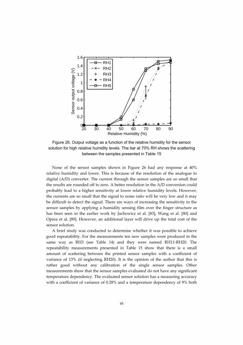
1.6
20 30 40 50 60 70 80 900
0.2
0.4
0.6
0.8
1
1.2
1.4
Relative Humidity (%)
Sen
sor
outp
ut v
olta
ge (
V)
RH1RH2RH3RH4RH5
Figure 26. Output voltage as a function of the relative humidity for the sensor solution for high relative humidity levels. The bar at 70% RH shows the scattering
between the samples presented in Table 15
None of the sensor samples shown in Figure 26 had any response at 40%
relative humidity and lower. This is because of the resolution of the analogue to
digital (A/D) converter. The current through the sensor samples are so small that
the results are rounded off to zero. A better resolution in the A/D conversion could
probably lead to a higher sensitivity at lower relative humidity levels. However,
the currents are so small that the signal to noise ratio will be very low and it may
be difficult to detect the signal. There are ways of increasing the sensitivity in the
sensor samples by applying a humidity sensing film over the finger structure as
has been seen in the earlier work by Jachowicz et al. [83], Wang et al. [80] and
Oprea et al. [89]. However, an additional layer will drive up the total cost of the
sensor solution.
A brief study was conducted to determine whether it was possible to achieve
good repeatability. For the measurements ten new samples were produced in the
same way as RH3 (see Table 14) and they were named RH11‐RH20. The
repeatability measurements presented in Table 15 show that there is a small
amount of scattering between the printed sensor samples with a coefficient of
variance of 13% (if neglecting RH20). It is the opinion of the author that this is
rather good without any calibration of the single sensor samples. Other
measurements show that the sensor samples evaluated do not have any significant
temperature dependency. The evaluated sensor solution has a measuring accuracy
with a coefficient of variance of 0.28% and a temperature dependency of 9% both
45
measured at 70% relative humidity. It has a cyclic stability of 15% at 50% relative
humidity and 0.08% at 85% relative humidity. The better stability at 85% relative
humidity is because of the higher current which gives a higher signal to noise ratio.
Table 15. Repeatability measurements on the relative humidity sensor samples at 70% relative humidity
RH11 RH12 RH13 RH14 RH15
0.75 V 0.63 V 0.78 V 0.60 V 0.85 V
RH16 RH17 RH18 RH19 RH20
0.85 V 0.86 V 0.87 V 0.84 V 1.55 V
The result shows that it is feasible to manufacture a two layer relative humidity
sensor, with a substrate and a conductive layer. It also shows that in order to make
a good sensor with as high sensitivity as possible, the spacing between the
electrodes in the conductive two‐dimensional structure should be as short as
possible and the conductivity in the electrodes should be as high as possible in
order to increase the DC current through the sensor.
3.3 Printed action activated moisture sensor
The action activated moisture sensor concept is based on a dry energy cell that
provides power to the readout electronic when activated by moisture. The concept
is based on the Action Activated Tags (AAT) concept described by Sidén et al. [90].
This means that when the detector is triggered, it powers up an electronic circuit
that initiates communication with an alarm server. Typical applications are
moisture and leakage detection in buildings and water pipes, moisture detection
and control of frozen food in smart packages and moisture and leakage detection
in health care systems.
For the moisture sensor concept to be competitive in the market segments
outlined, there are a number of demands which must be satisfied. Ideally, it should
have a long life time (i). It should be very low cost (ii). It should be possible to hide
or incorporate the device inside objects, for example, inside walls or in diapers (iii).
An active system that logs the moisture [91] and reports back if the moisture
content is too high could satisfy conditions (ii) and (iii), but fails to satisfy
condition (i) because of a built in energy source. Humidity indicators [92‐95] that
visually show whether the sensor has been exposed to harmful conditions easily
satisfies conditions (i) and (ii), but fails on condition (iii), because it is required to
be read visually. The action activated moisture sensor concept utilizing printed
energy cells described in this section meets the three conditions.
46

The concept is based on a printed energy cell that provides power to a readout
device when activated by moisture. There are many energy cell types using
different chemical compounds to store and provide power that could be used in
the outlined applications. For example lithium‐ion energy cells [96‐97], nickel‐
metal hydride energy cells [98‐99], zinc‐carbon energy cells [100‐101] and zinc‐air
energy cells [102]. The energy cells named cover the full range from partially
printable to fully printable. In the proposed concept, one of the most important
aspects is the cost. For a sensor to be placed in, for example, every diaper the
associated cost must be low. For this reason a zinc‐carbon type of energy cell is
used in the sensor concept presented in this section. The zinc‐carbon type is chosen
because it can be fully printed in conventional printing processes, which can drive
down the cost. The energy cell provides sufficient power to drive the readout
electronics and the necessary cost for the chemical components are relatively low,
which, all in all, offers a low cost energy cell.
The energy cell is a multilayer structure with two layers of paper. One paper is
printed using an ink mixture of zinc and carbon and the other by an ink mixture of
carbon and manganese dioxide. An electrolyte is placed between these two paper
layers. Normally printed energy cells have a well controlled electrolyte usually
including salts, such as zinc chloride or sodium chloride. In this case, water is used
as the electrolyte and thus the current driving capability will be much lower for the
dry cells than for normal printed batteries. When the moisture is entering into the
moisture absorbing separator layer of the energy cell structure, an electrochemical
reaction starts and the energy cell provides power to the readout electronics.
Different moisture absorbing substances can be used to tune the humidity
sensitivity of the dry energy cell. For example, in a diaper application, the trigger
level should be very close to 100% humidity while in moisture detection in
buildings the trigger level may be in the relative humidity level of 80 – 85% [35].
The moisture absorbing material can be doped with a mixture of ammonium
chloride and zinc chloride to increase the sensitivity of the sensor at low relative
humidity levels.
3.3.1 Experimental results for the action activated moisture sensor
In this section, the results from measurements on carbon‐zinc energy cell
samples are presented. The description of the sensor samples are presented in
Table 16. The sensor samples are produced by screen printing [58] the said
substrates (as seen in Table 16) with the carbon‐zinc and carbon‐manganese
dioxide ink mixtures. In between the substrates the said electrolyte (as seen in
Table 16) is placed. The active part of the evaluated energy cell samples has a
dimension of 15x30 mm. A picture of an energy cell can be seen in Figure 27. The
energy cell sensor will always be connected to some sort of readout device with a
47
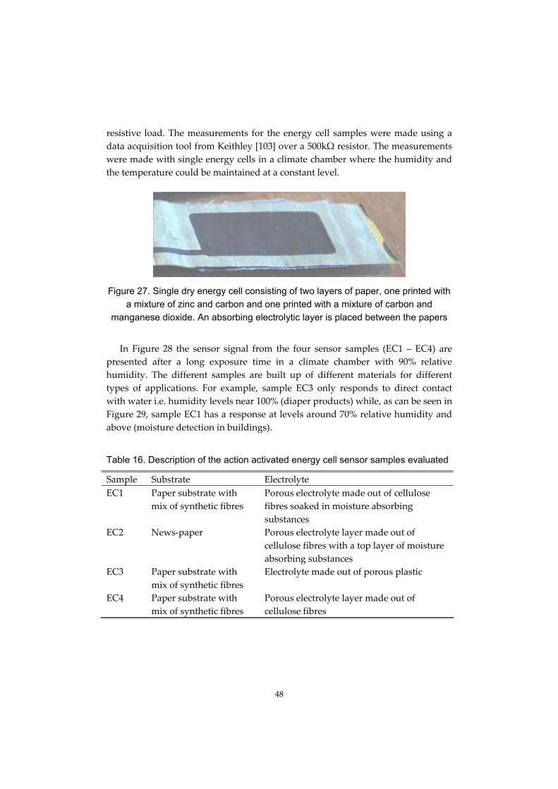
resistive load. The measurements for the energy cell samples were made using a
data acquisition tool from Keithley [103] over a 500kΩ resistor. The measurements
were made with single energy cells in a climate chamber where the humidity and
the temperature could be maintained at a constant level.
Figure 27. Single dry energy cell consisting of two layers of paper, one printed with
a mixture of zinc and carbon and one printed with a mixture of carbon and manganese dioxide. An absorbing electrolytic layer is placed between the papers
In Figure 28 the sensor signal from the four sensor samples (EC1 – EC4) are
presented after a long exposure time in a climate chamber with 90% relative
humidity. The different samples are built up of different materials for different
types of applications. For example, sample EC3 only responds to direct contact
with water i.e. humidity levels near 100% (diaper products) while, as can be seen in
Figure 29, sample EC1 has a response at levels around 70% relative humidity and
above (moisture detection in buildings).
Table 16. Description of the action activated energy cell sensor samples evaluated
Sample Substrate Electrolyte
EC1 Paper substrate with
mix of synthetic fibres
Porous electrolyte made out of cellulose
fibres soaked in moisture absorbing
substances
EC2 News‐paper Porous electrolyte layer made out of
cellulose fibres with a top layer of moisture
absorbing substances
EC3 Paper substrate with
mix of synthetic fibres
Electrolyte made out of porous plastic
EC4 Paper substrate with
mix of synthetic fibres
Porous electrolyte layer made out of
cellulose fibres
48
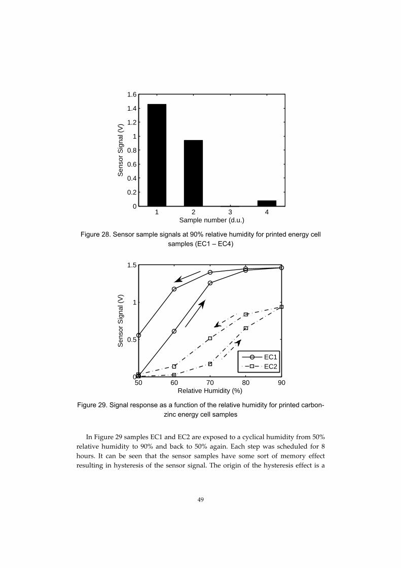
1.6
1 2 3 40
0.2
0.4
0.6
0.8
1
1.2
1.4
Sample number (d.u.)
Sen
sor
Sig
nal (
V)
Figure 28. Sensor sample signals at 90% relative humidity for printed energy cell samples (EC1 – EC4)
1.5
50 60 70 80 900
0.5
1
Relative Humidity (%)
Sen
sor
Sig
nal (
V)
EC1EC2
Figure 29. Signal response as a function of the relative humidity for printed carbon-zinc energy cell samples
In Figure 29 samples EC1 and EC2 are exposed to a cyclical humidity from 50%
relative humidity to 90% and back to 50% again. Each step was scheduled for 8
hours. It can be seen that the sensor samples have some sort of memory effect
resulting in hysteresis of the sensor signal. The origin of the hysteresis effect is a
49

thermodynamic process in the moisture absorption in the wood fibres [104], which
is the same process as for the moisture content sensor previously described. The
strength of the memory effect can be adjusted by selecting different materials in the
porous electrolytic layer. It is desirable to possess the hysteresis effect in an action
activated sensor, since it allows time for the registration to take place when the
sensor is triggered by a peak in the humidity. The memory effect provides energy
for data processing during a longer time than actually provided by the event itself.
The sensor solution can effectively be used as a “defrosting” alarm, for example
in frozen article monitoring systems in the supply chain. In this case the sensor is
preloaded with water and frozen together with the item to be monitored. When the
article is removed from the freezer or the temperature control fails the inner
electrode releases moisture and the sensor is triggered. Even when the sensor is
frozen some sensor signal (voltage) can be registered but the driving capability
(current) is extremely low. As can be seen in Figure 30, if the sensor sample is
maintained at room temperature, the signal increases and sensor becomes a power
generating element within a minute or less. The sensor sample evaluated in Figure
30 has been slightly modified in order to reduce current leakage when frozen and
thus the sensor sample only has a maximum signal level of 1.2 V.
Se
nso
rS
ign
al(V
)
1.4
1.2
1
0.8
0.6
0.4
0.2
0
Time (s)
0 50 100 150 200 250
Signal is unstable and weak infrozen condition
Full signal 1.2V withpower driving capability
Figure 30. Sensor signal from frozen sensor sample (EC4) as a function of time
after exposed to room temperature
The power driving capability from a single carbon‐zinc energy cell sensor
depends on the volume of the sensor. A typical sensor has a driving power of a few
mA and provides between 1.1 V to 1.5 V as a single cell. The difference in the
voltage level depends on the design of the sensor with respect to its chemistry and
layout. In order to reach the levels necessary to power the sensor platform
50

presented in section 2 the energy cells must provide above 1.8V in order to power
up the device. Thus, the dry energy cells are required to be stacked in series in
order to reach the power up level. One way of implementing the stacked dry
energy cells is by printing a top and a bottom substrate layer, which are then
laminated together to form the actual dry energy cell structure. In Figure 31 and
Figure 32 the different layers involved in the bottom and top substrates for a four
cell energy cell are presented. In Figure 33 a 3D picture of the four cells stacked
energy cell is shown. A two cell solution can easily be derived using half as many
cells as the structure shown in Figure 33.
Layer 1, silver paste Layer 2, solventbased carbon paste
2
Layer 3, solventbased carbon ink
doped with Zn
Layer 4, solventbased carbon inkdoped with MnO
(A) (B)
(C) (D)
Figure 31. Description of the bottom substrate layer of a four cell stacked energy
cell
The stack of dry cells will not be completely isolated electrically which means
that this configuration relies on the fact that the charge transport over the separator
is much stronger than the leakage between dry cells. The leakage between cells can
be minimized by the geometrical design of the stack.
51

Layer 1, solventbased carbon paste
Layer 2, solventbased carbon ink
doped with Zn
Layer 3, solventbased carbon inkdoped with MnO2
Layer 4, thinseparator layer
(A) (B)
(C) (D)
Figure 32. Description of the top substrate layer of a four cell stacked energy cell
Figure 33. 3D schematic picture of a four cell stacked energy cell
An initial study of the stacked dry cell structures was conducted using a
lamination technique and hand assembly. The different ink layers were screen
printed and laminated together as seen in Figure 33. As the separator layer, a low
52

cost filter paper with micrometer pores was used. The hand assembled energy cell
had an active area of 14 mm by 30 mm. In Table 17 the results from the initial
measurements using 3 ml of water can be seen.
Table 17. Current and voltage from typical hand assembled four cell stacked dry
cells structure. The open circuit voltage was 3.9V.
Load resistance Voltage Current Power
2.2 k 2.78 V 1.26 mA 3.5 mW
441 1.33 V 3.0 mA 4.0 mW
46 0.17 V 3.7 mA 0.63 mW
The results shown in Table 17 shows that stacked energy cells can be used to
power up the sensor platform to be used as a watch‐dog timer for moisture.
Sensor samples of single energy cells produced in batches show that the sensor
solution is very stable with less than 10% variation in signal for the same humidity
level using simple manual printing techniques. This value can of course be
improved by using better printing techniques. The sensors can be configured in
such a way that they provide substantial levels of electric power. For example, a
thin sensor the size of square decimetre can provide as much as 0.5 W in power
over several minutes.
The result shows that the concept of using carbon‐zinc energy cells as an action
activated moisture sensor is feasible. It also shows that the sensor can be
manufactured with different trigger and signal levels to enable it to be optimized
towards specific applications. The sensor can utilize the hysteresis effect of
hygroscopic materials, such as wood fibre based paper, to provide a stable
triggering signal.
3.4 Remote moisture sensor that utilizes ordinary RFID tags
The moisture sensing concept presented in this section has the ability to be read
remotely. Typical applications are remote moisture sensing and leakage detection
inside a building, for example, inside walls. Some technologies do exist in which it
is possible to remotely monitor the humidity inside walls. There are, for example,
microwave technologies [105‐106] in which a hole in the wall has to be drilled.
There are also surface acoustic wave (SAW) based sensors [78,107] and a resonant
frequency sensor [108], which has a reading range of about one centimetre. Active
wireless humidity loggers [109], require built‐in power supply, which means that
they possess a limited life time.
In this section a remote moisture sensor concept is proposed which utilizes
ordinary RFID tags. Two tags are incorporated into one label in which one of the
53

tags is embedded in a moisture absorbent material and the other is left open. In a
humid environment the moisture concentration is higher in the absorbent material
than in the surrounding environment, which causes degradation to the antenna of
the embedded tag in terms of dielectric losses and a change of input impedance.
The amount of water in the absorbent material is determined for a passive RFID
system by comparing the difference in the output power required to power up the
open and embedded tags respectively. For a semi‐passive RFID system the
difference in the backscattered signal strength is proportional to the moisture in the
absorbent material.
Labelinsidewall
Minimum required
RFIDReader
Wall
Opentag
Embedded
Moistureabsorbingmaterial
signal strength ishigher for embeddedtag than for open tag
tag
Figure 34. Remote moisture sensor label incorporating two RFID tags where one is
embedded in moisture absorbing material and the other is open
The sensors can be constructed at a very low cost because ordinary low cost
passive RFID tags can be used as remote moisture sensors, i.e. sensor signal inputs
are not required on the RFID chip. Figure 34 shows how a remote moisture sensor
label inside a wall could work. The idea is that the sensor label is inserted inside
the wall during the manufacture of the wall. The tag’s location is somehow
registered, for example, on the outside of the wall. The tags can then be read
periodically by means of a hand‐held reader and it is thus possible to prevent
costly damage due to mould or putrefaction in the building. By using passive RFID
tags that, in theory have an unlimited (in practice very long) life‐time (no built‐in
power supply), the remote moisture sensor concept can be used throughout the
entire life‐time of the building.
54

3.4.1 Experimental results for the remote moisture sensor solution
In this section the results from measurements for the remote moisture sensor
concept are presented. The measurements were made using two different RFID
systems. Firstly, a passive system was used, which was operating at a frequency of
865‐868 MHz and secondly, a semi‐passive system, operating at a frequency of 2.45
GHz was used. The passive measurements were made using EPC Gen 2 tags from
Alien Technologies [110] and which measured 95 mm x 8 mm. The embedded tag
was covered with papers whose dimensions were 103 mm x 20 mm. The semi‐
passive measurements were made using tags from TagMaster [111] measuring 85
mm x 54 mm. In this case the embedded tag was covered with papers that had a
dimension of 90 mm x 58 mm. In the passive system the measurements were made
using two tags simultaneously, one open and one embedded according to Table 18.
By comparing the power difference required to power up the two tags
respectively, the moisture content in the absorbing material could be determined.
The measurements for the semi‐passive RFID system were made using only one
tag at a time because the reader set‐up only allowed a direct readout of the
backscattered signal. Since this is the total received strength, the investigation
could only be made for one tag at the time and not for pairs of tags. The concept is,
however, directly applicable for pairs of tags if a reader can be constructed which
is able to extract individual backscattering powers. At present, the difference in
backscattered power is extracted from the same tag when it is open and when it is
embedded in paper and not simultaneously for two backscattered tags.
Table 18. Description of the remote moisture sensor samples evaluated
Sample RFID system Tag 1 (embedded tag) Tag 2
P1 Passive ‐ 868 MHz Open Open
P2 Passive ‐ 868 MHz 5 mm blotting paper in front Open
P3 Passive ‐ 868 MHz 5 mm blotting paper in front
and behind
Open
SP1 Semi‐passive ‐ 2.45 GHz * 2.5 mm blotting paper in front Open
SP2 Semi‐passive ‐ 2.45 GHz * 5 mm blotting paper in front Open
SP3 Semi‐passive ‐ 2.45 GHz * 5 mm of Luna Core [112]
paper in front
Open
* Measurements with one RFID tag at a time
Figure 35 and Figure 36 show the results from measurements on the remote
moisture sensor samples described in Table 18 as a function of the relative
humidity. The measurements were made in a climate room where the relative
humidity and temperature could be maintained at a constant predetermined level.
55

The time intervals between the measurements were 24 hours. The results in Figure
35 show that at 50% relative humidity there is no difference between the open and
the embedded tags. However at 90% relative humidity there is about a 5 dB
difference. The sensor sample that is embedded with blotting paper both in front
and behind (P3) shows a little higher difference than the sensor sample with only
the blotting paper in front (P2).
50 60 70 80 900
1
2
3
4
6
5
Relative Humidity (%)
Tra
nsm
itted
Pow
er D
iffer
ence
(dB
)
P1P2P3
Figure 35. Minimum output power difference required for the RFID reader to read
the open and the embedded passive tags as a function of the relative humidity
The semi‐passive RFID system shown in Figure 36 shows an increased
backscattered power at higher humidity levels. This is the reason for the inclusion
of negative numbers. The phenomenon of increased backscattering is possibly
because the impedance of the tags becomes even closer to a perfect matching than
for the original tag antenna, which leads to an increased reading range. The
introduced ohmic losses would then have a smaller effect than the increase in
impedance match. The result shows a 1.5 dB stronger backscattering power for the
embedded tag at 50% relative humidity and 4 dB at 90% for sensor sample SP2.
This provides a 2.5 dB difference between 50% and 90% relative humidity as
opposed to the passive system which had a 5 dB difference.
56

−0.5
50 60 70 80 90−4.5
−4
−3.5
−3
−2.5
−2
−1.5
−1
Relative Humidity (%)
Bac
ksca
ttere
d P
ower
Diff
eren
ce (
dB
)
SP1SP2SP3
Figure 36. Backscattering power difference between open and embedded semi-passive RFID tags as a function of the relative humidity
14
0 2 4 6 8 10 120
2
4
6
8
10
12
Amount of Added Water (g)
Tra
nsm
itted
Pow
er D
iffer
ence
(dB
)
P2P3
Figure 37. Minimum output power difference required for the RFID reader to read the open and the embedded passive tags as a function of the amount of added
water to the moisture absorbing material
Figure 37 and Figure 38 show the results from measurements on the sensor
samples, presented in Table 18, in situations of real wetness. In this case, water is
applied directly onto the moisture absorbing material. Water drops are added one
57

drop at the time with the aid of a pipette and distributed at about five drops per
gram. The measurements were conducted approximately two minutes after the
application of the water. A real life comparison to this real wetness situation could
be when the labels are placed in locations inside walls or in floors and where there
is a risk of water leakage, for example, from leaking water pipes.
For the measurements with the passive sensor samples shown in Figure 37
there is a 13 dB difference of the transmitted power required to power up the
embedded tag when 12 grams of water is applied to the paper sheets in
comparison to dry paper sheets.
For the measurements on the semi‐passive sensor samples shown in Figure 38
the same behaviour can be seen as in the case for climate room measurements
(Figure 36) where there is an increased backscattering power for a small amount of
added water to the paper sheets. However, when the amount of water exceeds five
grams the system shows a decreased backscattered power. If the initial negative
values are ignored, the difference for the semi‐passive system is slightly smaller
than for the passive system. It should, however, be remembered that the semi‐
passive tag is covered by paper sheets of a larger area than the passive tags, but the
comparison is made using the same amount of water.
0 2 4 6 8 10 12 14−5
0
5
10
Amount of Added Water (g)
Bac
ksca
ttere
d P
ower
Diff
eren
ce (
dB)
SP1SP2
Figure 38. Backscattering power difference between open and embedded semi-
passive RFID tags as a function of the amount of added water to the moisture absorbing material
The results show that the concept for remote moisture sensors using ordinary
RFID tags is feasible. The difference in power level is of the order of approximately
58
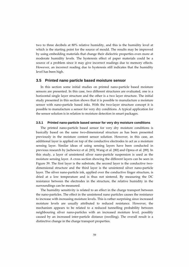
two to three decibels at 80% relative humidity, and this is the humidity level at
which is the starting point for the source of mould. The results may be improved
by using embedding materials that change their dielectric properties even more at
moderate humidity levels. The hysteresis effect of paper materials could be a
source of a problem since it may give incorrect readings due to memory effects.
However, an incorrect reading due to hysteresis still indicates that the humidity
level has been high.
3.5 Printed nano particle based moisture sensor
In this section some initial studies on printed nano‐particle based moisture
sensors are presented. In this case, two different structures are evaluated, one is a
horizontal single layer structure and the other is a two layer structure. The initial
study presented in this section shows that it is possible to manufacture a moisture
sensor with nano‐particle based inks. With the two‐layer structure concept it is
possible to manufacture a sensor for very dry conditions. A typical application for
the sensor solution is in relation to moisture detection in smart packages.
3.5.1 Printed nano-particle based sensor for very dry moisture conditions
The printed nano‐particle based sensor for very dry moisture conditions is
basically based on the same two‐dimensional structure as has been presented
previously in the moisture content sensor solution. However, in this case, an
additional layer is applied on top of the conductive electrodes to act as a moisture
sensing layer. Similar ideas of using sensing layers have been conducted in
previous research by Jachowicz et al. [83], Wang et al. [80] and Oprea et al. [89]. In
this study, a layer of unsintered silver nano‐particle suspension is used as the
moisture sensing layer. A cross section showing the different layers can be seen in
Figure 39. The first layer is the substrate, the second layer is the conductive two‐
dimensional structure and the third layer is the unsintered silver nano‐particle
layer. The silver nano‐particle ink, applied over the conductive finger structure, is
dried at a low temperature and is thus not sintered. By measuring the DC
resistance between the electrodes in the structure, the relative humidity in the
surroundings can be measured.
The humidity sensitivity is related to an effect in the charge transport between
the nano‐particles. The effect in the unsintered nano particles causes the resistance
to increase with increasing moisture levels. This is rather surprising since increased
moisture levels are usually attributed to reduced resistance. However, the
mechanism appears to be related to a reduced tunnelling probability between
neighbouring silver nano‐particles with an increased moisture level, possibly
caused by an increased inter‐particle distance (swelling). The overall result is a
distinctive change in the charge transport properties.
59
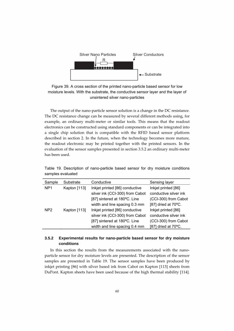
R
Silver Conductors
Substrate
Silver Nano Particles
Figure 39. A cross section of the printed nano-particle based sensor for low moisture levels. With the substrate, the conductive sensor layer and the layer of
unsintered silver nano-particles
The output of the nano‐particle sensor solution is a change in the DC resistance.
The DC resistance change can be measured by several different methods using, for
example, an ordinary multi‐meter or similar tools. This means that the readout
electronics can be constructed using standard components or can be integrated into
a single chip solution that is compatible with the RFID based sensor platform
described in section 2. In the future, when the technology becomes more mature,
the readout electronic may be printed together with the printed sensors. In the
evaluation of the sensor samples presented in section 3.5.2 an ordinary multi‐meter
has been used.
Table 19. Description of nano-particle based sensor for dry moisture conditions samples evaluated
Sample Substrate Conductive Sensing layer
NP1 Kapton [113] Inkjet printed [86] conductive silver ink (CCI-300) from Cabot [87] sintered at 180ºC. Line
width and line spacing 0.3 mm
Inkjet printed [86] conductive silver ink (CCI-300) from Cabot
[87] dried at 70ºC.
NP2 Kapton [113] Inkjet printed [86] conductive
silver ink (CCI-300) from Cabot [87] sintered at 180ºC. Line width and line spacing 0.4 mm
Inkjet printed [86]
conductive silver ink (CCI-300) from Cabot [87] dried at 70ºC.
3.5.2 Experimental results for nano-particle based sensor for dry moisture conditions
In this section the results from the measurements associated with the nano‐
particle sensor for dry moisture levels are presented. The description of the sensor
samples are presented in Table 19. The sensor samples have been produced by
inkjet printing [86] with silver based ink from Cabot on Kapton [113] sheets from
DuPont. Kapton sheets have been used because of the high thermal stability [114].
60
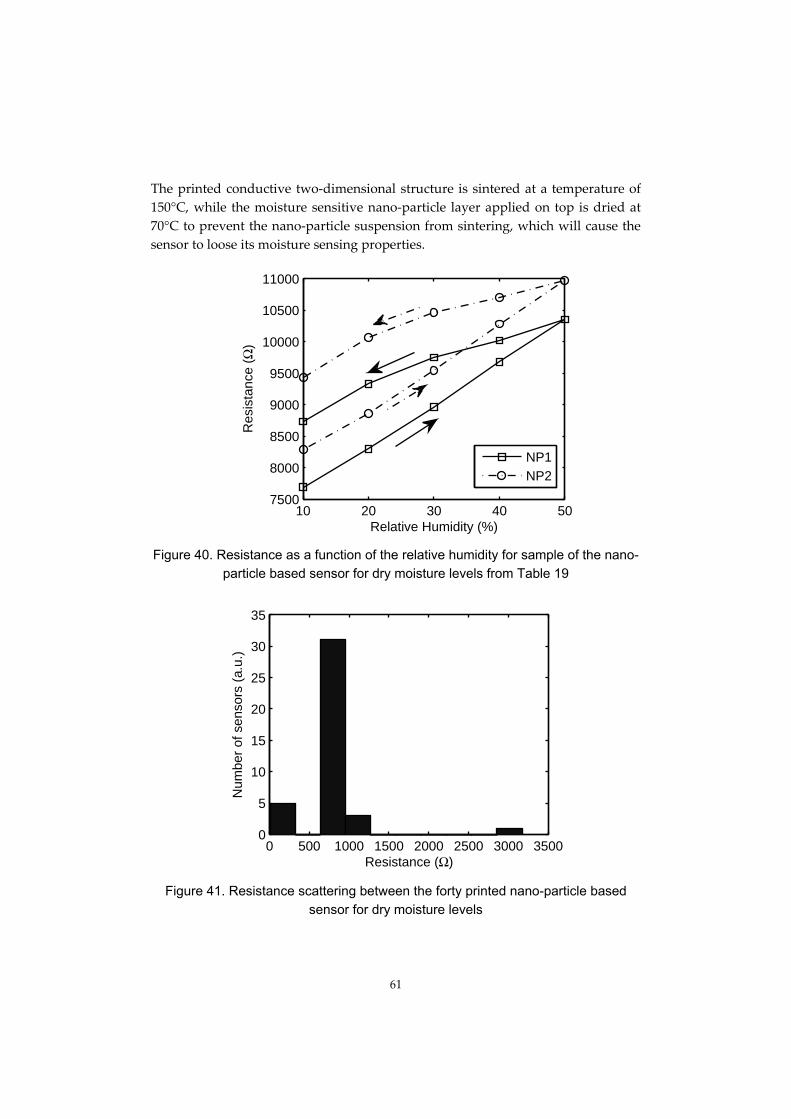
The printed conductive two‐dimensional structure is sintered at a temperature of
150°C, while the moisture sensitive nano‐particle layer applied on top is dried at
70°C to prevent the nano‐particle suspension from sintering, which will cause the
sensor to loose its moisture sensing properties.
10 20 30 40 507500
8000
8500
9000
9500
10000
10500
11000
Relative Humidity (%)
Res
ista
nce
(Ω)
NP1NP2
Figure 40. Resistance as a function of the relative humidity for sample of the nano-particle based sensor for dry moisture levels from Table 19
35
0 500 1000 1500 2000 2500 3000 35000
5
10
15
20
25
30
Resistance (Ω)
Num
ber
of s
enso
rs (
a.u.
)
Figure 41. Resistance scattering between the forty printed nano-particle based sensor for dry moisture levels
61
In Figure 40 the results from the nano‐particle sensor samples measured in a
climate chamber in which the relative humidity was altered from 10% up to 50%
and back to 10% are presented. The sensor samples have a slow response time with
a saturation time of about 12 hours. To ensure that the sensor samples are stable at
the corresponding relative humidity level they were stored in the chamber for 24
hours between each measurement. The results show that the sensor samples are
linear from 10% to 50% relative humidity. However, when the relative humidity
level is reduced down to 10% again the sensor samples shows a hysteresis effect.
The measurements could only be conducted at relative humidity levels up to 50%
because the unsintered nano layer becomes liquefied at higher relative humidity
levels.
A brief study was conducted to determine whether it was possible to achieve
good repeatability. In this study, 40 sensor samples were produced in a batch. As
can be seen in Figure 41, there is some scattering between the sensor samples and,
in fact, between the 40 samples there is a coefficient of variance of 56% which was
not felt to be good. However, between 30 of the samples there is a variance of 8%
which is rather good without calibration of the single sensor samples.
The sensor samples show no significant temperature dependency over the
measured range. However, at very high temperatures namely above 100°C the
unsintered silver nano‐particle layer will be sintered and the moisture sensitivity
will be lost.
The result shows that it is feasible to manufacture a printed relative humidity
sensor for very low humidity levels. 75% of the sensor samples had a variance of
8% without calibration of the single samples. The sensor samples show a linear
response as the relative humidity is increased from 10% to 50%. However, the
sensor shows a hysteresis effect when the relative humidity is reduced down to
10%.
3.5.3 Single layer nano-particle based moisture sensor for high humidity levels
In this section a printed single layer nano‐particle based moisture sensor is
presented. The sensor is based on a short and narrow line of silver nano‐particles,
as seen in Figure 42(a). When the silver nano‐particle is exposed to water or
humidity, the resistance of the sensor is decreased and remains at that level after
drying. The sensor can, for example, be used to monitor humidity in the
transportation of packages or in buildings. The observed reduction of the
resistance in the nano‐particle ink line is related to the sintering of the nano‐
particles. The sintering of nano‐particle inks is usually performed by heating in an
oven or electrically [115‐118], although some results on chemical sintering have
62

been reported [119‐120]. The active sizes for the width and the length of the thin
line in Figure 42(a) are 40 μm and 125 μm respectively between the contact pads. If
the initial or final resistance in the sensor requires to be lower for a particular
application, then multiple lines can be used as shown in Figure 42(b). All the
measurements in this study are based on the single line version of the nano‐
particle based moisture sensor as seen in Figure 42(a).
(a) (b)
Figure 42. Photographs showing single line single layer nano-particle based moisture sensor (a) and multiple line single layer nano-particle based moisture
sensor (b). Both with an active length of 125 µm
The single layer nano‐particle structure described in this section was initially
designed as a printed write once read many times (WORM) resistive memory that
can be programmed using a 1.5 V printed battery and to be used as a wireless
watch‐dog alarm function. However, in this case it is used as a moisture sensitive
sensor.
3.5.4 Experimental results for single layer nano-particle based moisture sensor
In this section the results from moisture measurements on the single layer nano‐
particle based moisture sensor are presented. The sensor evaluated in this study
was inkjet printed [86] with Silverjet DGP 40LT‐15C [121] ink from Advanced
Nano Products (ANP) [122] on HP Advanced photo paper [84]. In Figure 43 the
layout of the printed sensor samples with eight sensor elements can be seen. The
layout is designed to fit into a standard SD [123] memory card reader for easy
characterization and evaluation of the sensor. The samples evaluated were
prepared by printing the silver nano‐particle ink with a Dimatix DMP‐2831 [124]
inkjet printer using 10 picoliter printing heads. After being printed, the resistance
of the print was usually very high (above 15 MΩ) so the samples where dried for a
63

short time in the oven at 80 – 90°C so that the resistance reduced to around 2 MΩ
to 10 MΩ. After the oven treatment, the samples were electrically sintered down to
the desired initial resistance value. The electrical sintering, in comparison to heat
sintering, makes it easier to control the resistance value in the preparation of the
samples.
Figure 43. Layout of the single layer nano-particle moisture sensor with eight sensor elements
106
100
102
104
106
100
102
104
Initial resistance (Ω)
Rel
ativ
e re
sist
ance
cha
nge
(a.u
.)
Figure 44. Measured relative resistance change of single layer nano-particle based sensors with different initial resistance values subjected to 90% RH for 24 hours
It has been observed that the initial resistance value affects how large the
relative resistance change is when the sensors are subjected to humidity. In Figure
44 sensor samples with different initial resistance values were subjected to 90% RH
and 23°C for a period of 24 hours. The resistance was measured before they were
64

placed in the climate chamber and after they have been removed and dried in 30%
RH.
In Figure 45 the final resistance for the sensor samples shown in Figure 44 is
plotted with respect to the initial resistance. It can be seen that the final resistance
is very consistent and varies only from 40Ω to 105Ω although the initial resistance
is within the range from 1kΩ to 10MΩ. For values below 1kΩ the final resistance
slowly decreases until it reaches a value of 2Ω for an initial value of 5Ω.
102
104
106
100
101
102
Fin
al r
esis
tanc
e (Ω
)
Initial resistance (Ω)
Figure 45. Final resistance as a function of the initial resistance for the single layer nano-particle based moisture sensor shown in Figure 44
Measurements performed on single layer nano‐particle based moisture sensor
samples in different humidity levels can be seen in Figure 46. Here, the sensor
samples were electrically sintered down to between 3kΩ and 5kΩ. After the
electrical sintering, the samples were exposed to different relative humidity levels
where the resistance was logged using a Kiethley 2410 sourcemeter [103]. The
measurements were made in a climate chamber where the temperature was held at
a constant level of 23°C. As can be seen, the resistance decreases more rapidly at
higher humidity levels. Thus, by logging the resistance change in the sensor and by
calculating the slope of the resistance change the relative humidity can be
determined. After the moisture measurements in the climate chamber the samples
were exposed to a low relative humidity level of 30% which causes the resistance
decrease to stop and the resistance in the samples remained at the corresponding
resistance level from the end of the measurements.
65

0 5 10 15 20 25 30 3510
−3
10−2
10−1
100
Time (h)
90% RH80% RH
Nor
mal
ised
res
ista
nce
(a.u
.)
70% RH60% RH30% RH
Figure 46. Measurements showing resistance change in different humidity levels for single layer nano-particle sensors printed on HP Advanced photo paper
0 5 10 15 20 25 30 3510
−3
10−2
10−1
100
101
Time (h)
Nor
mal
ised
res
ista
nce
(a.u
.)
90% RH80% RH70% RH60% RH
Figure 47. Measurements showing resistance change in different humidity levels for single layer nano-particle based sensors printed on Canon PT-101 photo paper
It has been observed that when using other photo paper brands, such as the
Canon PT‐101 photo paper [125], the resistance change when exposed to high
humidity levels is completely different as seen in Figure 47. This is felt to be very
likely due to different coating layers in the photo papers.
66

Nano‐particle inks are usually stabilized with one or more capping agents that
create an electrostatic and/or steric barrier that prevents the nano‐particles from
aggregating. Polyvinylpyrrolidone (PVP), which is a well known capping agent,
was established to be present in the ANP ink by pyrolysis GC/MS [126]. In earlier
work in chemical sintering [119, 120] of silver nano‐particles it has been shown that
when neutralizing the charges in the capping agent this leads to particle
coalescence and sintering of the silver nano‐particles. When examining the results
in Figure 46 it can be seen that the humidity threshold at which the resistance starts
to decrease is in the same humidity range as when the PVP is known to soften and
therefore the resistance decrease could be explained by particle coalescence.
However, this does not explain the different results obtained from different photo
paper brands. It could be that that one portion of the PVP is bound to the particle
and the excess can be pulled into the coating by the capillary forces and therefore
the pore structure will determine the amount of polymer retained in the ink layer.
Also, when the moisture content in the PVP is raised, the ability for there to be ion
transport is created within the polymer [127] and ions from the paper coating can
be transported into the ink layer. It is a possibility that the chemistry of the paper is
also of importance for the sintering process. Therefore, the observed variation in
moisture sensitivity on papers of different brands could possibly be explained by
variables in the coatings. More research is required to be able fully understand the
humidity sintering effect on the silver nano‐particle inks and the role of the
substrate in the process.
A short study conducted shows that when using Cabot CCI‐300 [87] on HP
Advanced photo paper the resistance will instantly become very low and that
either none or only a very small moisture sensitivity could be seen when there was
exposure to high moisture levels.
The single layer nano‐particle moisture sensor is an irreversible sensor and can
therefore only be used once. This could be a drawback, but, on the other hand, the
sensor has a memory effect that provides information that the sensor has been
exposed to a high humidity level, which is very crucial information in certain
applications.
The result in this section shows that it is feasible to manufacture printed single
layer and two‐layer nano‐particle based relative humidity sensors. However, more
research is required in order to fully understand the moisture sintering of the silver
nano‐particles and the influence by the substrate. For further understanding of the
moisture sintering the reference is to future work within the “New system
integration tools for printed intelligence in packaging applications” project at Mid
Sweden University [128].
67

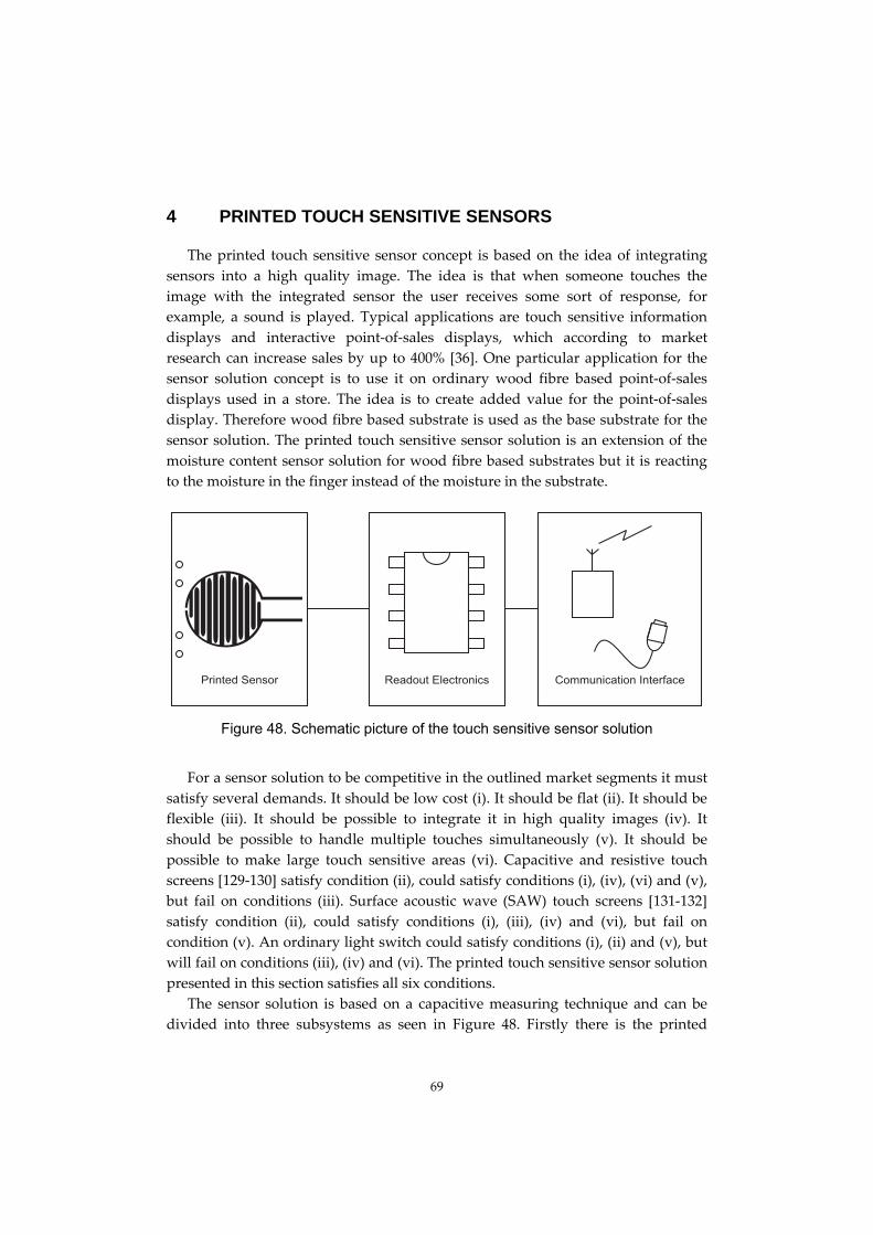
69
4 PRINTED TOUCH SENSITIVE SENSORS
The printed touch sensitive sensor concept is based on the idea of integrating
sensors into a high quality image. The idea is that when someone touches the
image with the integrated sensor the user receives some sort of response, for
example, a sound is played. Typical applications are touch sensitive information
displays and interactive point‐of‐sales displays, which according to market
research can increase sales by up to 400% [36]. One particular application for the
sensor solution concept is to use it on ordinary wood fibre based point‐of‐sales
displays used in a store. The idea is to create added value for the point‐of‐sales
display. Therefore wood fibre based substrate is used as the base substrate for the
sensor solution. The printed touch sensitive sensor solution is an extension of the
moisture content sensor solution for wood fibre based substrates but it is reacting
to the moisture in the finger instead of the moisture in the substrate.
Printed Sensor Readout Electronics Communication Interface
Figure 48. Schematic picture of the touch sensitive sensor solution
For a sensor solution to be competitive in the outlined market segments it must
satisfy several demands. It should be low cost (i). It should be flat (ii). It should be
flexible (iii). It should be possible to integrate it in high quality images (iv). It
should be possible to handle multiple touches simultaneously (v). It should be
possible to make large touch sensitive areas (vi). Capacitive and resistive touch
screens [129‐130] satisfy condition (ii), could satisfy conditions (i), (iv), (vi) and (v),
but fail on conditions (iii). Surface acoustic wave (SAW) touch screens [131‐132]
satisfy condition (ii), could satisfy conditions (i), (iii), (iv) and (vi), but fail on
condition (v). An ordinary light switch could satisfy conditions (i), (ii) and (v), but
will fail on conditions (iii), (iv) and (vi). The printed touch sensitive sensor solution
presented in this section satisfies all six conditions.
The sensor solution is based on a capacitive measuring technique and can be
divided into three subsystems as seen in Figure 48. Firstly there is the printed

sensor structure which is connected to a detection or readout electronic device. The
readout electronic device converts the analogue capacitive sensor signal into a
digital format which is sent to an external device through the communication
interface. The external device can be any type of electric device, for example a
computer, an mp3 player or a light switch.
4.1 Printed sensor structure for the touch sensitive sensor solution
The first part of the touch sensitive sensor solution is the printed sensor
structure. The sensor structure is based on a capacitive measuring technique. There
are many ways of manufacturing capacitive sensor structures from a single layer
[133] to multilayer structures [134]. One aim associated with this sensor solution is
to produce low cost sensor structures and therefore a single layer structure is
preferred in order to reduce the manufacturing cost. When using a single layer
capacitive touch sensor solution the sensor is triggered by the capacitance created
between the human hand and the sensor structure. By using a parallel pair
electrode concept in the sensor the sensitivity can be increased, as the human hand
is touching both of the electrodes. This is the reason why the sensor is based on a
two‐dimensional conductive structure, of which an example can be seen in Figure
18.
The printed sensor structure is fabricated using conductive ink on paper
substrates. The sensor structure is built up of four layers. Firstly there is a wood
fibre based substrate, secondly there is a dielectric or insulating layer, thirdly there
is a conductive layer and finally there is a cover layer, see Figure 49.
R2
C2 C2
C1
Conductive
Dielectric
Substrate
Cover
Figure 49. A cross section of the capacitive touch sensitive sensor solution
The first layer, namely the wood fibre based substrate, is used because it is a
low cost material with good printability. However the disadvantage associated
with wood fibre based substrates is that it changes its conductivity when the
70
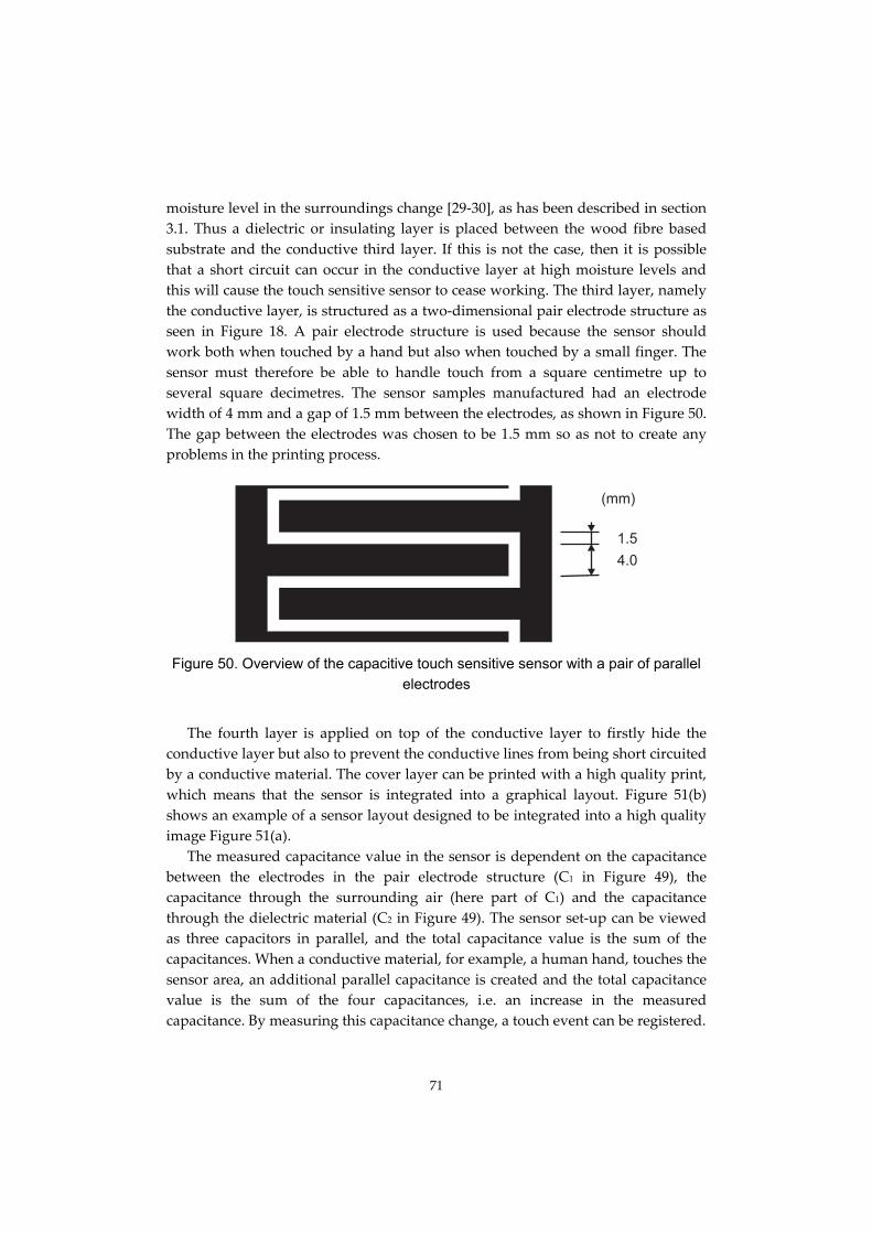
moisture level in the surroundings change [29‐30], as has been described in section
3.1. Thus a dielectric or insulating layer is placed between the wood fibre based
substrate and the conductive third layer. If this is not the case, then it is possible
that a short circuit can occur in the conductive layer at high moisture levels and
this will cause the touch sensitive sensor to cease working. The third layer, namely
the conductive layer, is structured as a two‐dimensional pair electrode structure as
seen in Figure 18. A pair electrode structure is used because the sensor should
work both when touched by a hand but also when touched by a small finger. The
sensor must therefore be able to handle touch from a square centimetre up to
several square decimetres. The sensor samples manufactured had an electrode
width of 4 mm and a gap of 1.5 mm between the electrodes, as shown in Figure 50.
The gap between the electrodes was chosen to be 1.5 mm so as not to create any
problems in the printing process.
1.5
4.0
(mm)
Figure 50. Overview of the capacitive touch sensitive sensor with a pair of parallel electrodes
The fourth layer is applied on top of the conductive layer to firstly hide the
conductive layer but also to prevent the conductive lines from being short circuited
by a conductive material. The cover layer can be printed with a high quality print,
which means that the sensor is integrated into a graphical layout. Figure 51(b)
shows an example of a sensor layout designed to be integrated into a high quality
image Figure 51(a).
The measured capacitance value in the sensor is dependent on the capacitance
between the electrodes in the pair electrode structure (C1 in Figure 49), the
capacitance through the surrounding air (here part of C1) and the capacitance
through the dielectric material (C2 in Figure 49). The sensor set‐up can be viewed
as three capacitors in parallel, and the total capacitance value is the sum of the
capacitances. When a conductive material, for example, a human hand, touches the
sensor area, an additional parallel capacitance is created and the total capacitance
value is the sum of the four capacitances, i.e. an increase in the measured
capacitance. By measuring this capacitance change, a touch event can be registered.
71
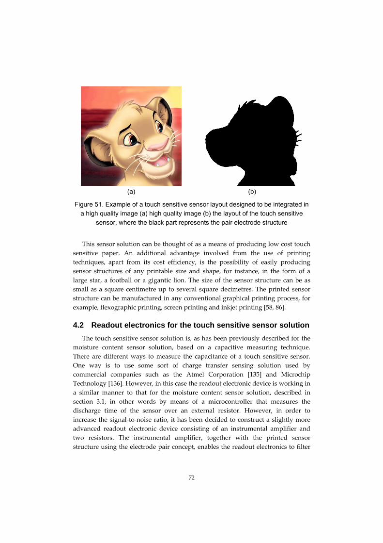
(a) (b)
Figure 51. Example of a touch sensitive sensor layout designed to be integrated in a high quality image (a) high quality image (b) the layout of the touch sensitive
sensor, where the black part represents the pair electrode structure
This sensor solution can be thought of as a means of producing low cost touch
sensitive paper. An additional advantage involved from the use of printing
techniques, apart from its cost efficiency, is the possibility of easily producing
sensor structures of any printable size and shape, for instance, in the form of a
large star, a football or a gigantic lion. The size of the sensor structure can be as
small as a square centimetre up to several square decimetres. The printed sensor
structure can be manufactured in any conventional graphical printing process, for
example, flexographic printing, screen printing and inkjet printing [58, 86].
4.2 Readout electronics for the touch sensitive sensor solution
The touch sensitive sensor solution is, as has been previously described for the
moisture content sensor solution, based on a capacitive measuring technique.
There are different ways to measure the capacitance of a touch sensitive sensor.
One way is to use some sort of charge transfer sensing solution used by
commercial companies such as the Atmel Corporation [135] and Microchip
Technology [136]. However, in this case the readout electronic device is working in
a similar manner to that for the moisture content sensor solution, described in
section 3.1, in other words by means of a microcontroller that measures the
discharge time of the sensor over an external resistor. However, in order to
increase the signal‐to‐noise ratio, it has been decided to construct a slightly more
advanced readout electronic device consisting of an instrumental amplifier and
two resistors. The instrumental amplifier, together with the printed sensor
structure using the electrode pair concept, enables the readout electronics to filter
72

out the noise picked up in the sensor structure, which leads to an increased signal–
to‐noise ratio. The readout electronic device used in the evaluation of the sensor
samples is charging the sensor structures to five volts and is measuring the
discharge time over a 100kΩ resistor. The sensors are discharged to a low TTL
level (0.8 V) and thus an all digital electronic device is used. The readout electronic
device can easily be integrated into standard electronics solutions or into a single
chip solution.
4.3 Communication interface for the touch sensitive sensor solution
When the readout electronic device has detected a touch on the printed sensor,
an event has to be sent to an external device which gives a feedback to the user.
The feedback could, for instance, be to play a sound or switching a light bulb on or
off. To be able to communicate with the external device a communication interface
is required. The communication interface can be divided into two system groups.
Firstly, there is a simpler version with a simple analogue wire solution, which
means that a wire is placed between the readout electronic device and the external
device. This is useful when the distance between the printed sensor and the
external device is short. The whole system can, for example, be integrated into the
same unit. However, for longer distances, it may prove difficult to have a wired
communication and, in this case, it is more beneficial to use a more advanced
sensor concept which is based on a distributed sensor network with wireless
communication links. In a wireless system, the readout electronic device (sensor
node) is working alone and communicates with a central node that triggers the
external device when a touch has been registered. More than one sensor node can
be used in this set‐up. In Table 20 there is a comparison between four possible
wireless standards for use in creating a distributed sensor network.
Table 20. Comparison of different wireless standards [137-139]
Name Wi‐Fi Bluetooth Semi‐active
RFID
Zigbee
Standard IEEE 802.11b IEEE 802.15.1 EPC IEEE 802.15.4
Network Size 30 7 > 100 65536
Data Rate 11 Mbps 1 Mbps 30 kbps 250 kbps
Range 100 m 10 m 5 m 30 m
Power Consumption
‐ Active 100 mW 48 mW 1 mW 40 mW
‐ Sleep 180 μW 1 μW 40 μW
73
In a distributed sensor network the sensor nodes are working by themselves
and therefore the power consumption is very important for a sensor network to
work efficiently. In an interactive point‐of‐sales display system the data rate of the
sensor network is not overly important because a relatively small amount of data
will be sent through the network. However the network size may by very
important if the sensor network is working in, for example, a supermarket with
multiple displays. In the case of a point‐of‐sales display solution with multiple
displays the ZigBee communication interface would be preferred because of its
large network size, long communication range and low power consumption. In
other applications, such as, packaging solutions where the sensor is printed on a
package and when the package is picked up, an event will be activated. A semi‐
active RFID communication system is better for this scenario as it has very low
power consumption.
4.4 Experimental results for the touch sensitive sensor solution
Table 21. Description of the touch sensitive sensor samples evaluated
Sample Substrate Dielectric Conductive Cover layer
TS1 Single wall C-flute
[77] corrugated board made out of kraftliner [61]
100 µm
thick plastic film from MACtac
[60]
Screen printed [58]
conductive silver ink (26-8204) from Coates Screen [59]
100 µm thick
plastic film from MACtac [60]
TS2 Single wall C-flute
[77] corrugated board made out of testliner [61]
100 µm
thick plastic film from MACtac
[60]
Screen printed [58]
conductive silver ink (26-8204) from Coates Screen [59]
100 µm thick
plastic film from MACtac [60]
TS3 Single wall C-flute [77] corrugated
board made out of kraftliner [61]
100 µm thick plastic
film from MACtac [60]
Screen printed [58] conductive carbon
ink (26-8203) from Coates Screen [59]
100 µm thick plastic film
from MACtac [60]
In this section the results from measurements on three touch sensitive sensor
samples are presented. The description of the sensor samples are presented in
Table 21 with the different layers presented in Figure 49. In the evaluated sensor
samples, a plastic film was used as the dielectric layer because of an easier
74
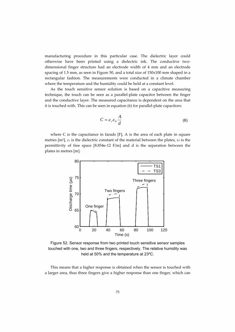
manufacturing procedure in this particular case. The dielectric layer could
otherwise have been printed using a dielectric ink. The conductive two‐
dimensional finger structure had an electrode width of 4 mm and an electrode
spacing of 1.5 mm, as seen in Figure 50, and a total size of 150x100 mm shaped in a
rectangular fashion. The measurements were conducted in a climate chamber
where the temperature and the humidity could be held at a constant level.
As the touch sensitive sensor solution is based on a capacitive measuring
technique, the touch can be seen as a parallel‐plate capacitor between the finger
and the conductive layer. The measured capacitance is dependent on the area that
it is touched with. This can be seen in equation (6) for parallel‐plate capacitors:
d
AC r 0 (6)
where C is the capacitance in farads [F], A is the area of each plate in square
metres [m2], εr is the dielectric constant of the material between the plates, ε0 is the
permittivity of free space [8.854e‐12 F/m] and d is the separation between the
plates in metres [m].
0 20 40 60 80 100 12060
65
70
75
80 TS1TS3
Time (s)
Dis
char
ge ti
me
(µs)
One finger
Two fingers
Three fingers
Figure 52. Sensor response from two printed touch sensitive sensor samples
touched with one, two and three fingers, respectively. The relative humidity was held at 50% and the temperature at 23ºC.
This means that a higher response is obtained when the sensor is touched with
a larger area, thus three fingers give a higher response than one finger, which can
75

be seen in Figure 52. The result also shows that there is no significant influence of
the sheet resistivity of the conductive layer. This is an important fact because the
price of the carbon based ink is approximately 10% of the silver based ink. The
carbon based ink has a sheet resistivity of 18Ω/ and the silver based ink has a
sheet resistivity of 0.02Ω/. Both of these cases involve a layer thickness of 15 μm.
In Figure 53 a change can be seen in the base value (when the sensor sample is
untouched) in comparison to Figure 52. The difference is that the measurement
shown in Figure 53 is made with a relative humidity of 85% in comparison to 50%
in Figure 52. As seen in the moisture content sensors for wood fibre based
substrates (section 3.1.1) and research by Simula et al [59] and Murphy [30] that the
conductivity of wood fibre based substrates is dependent on the moisture content
of the paper. The conductivity change in the evaluated substrate has changed the
base value of the sensor sample. However, the touch sensitivity still remains the
same. There is, however, a small tendency for a higher noise level at 85% relative
humidity in comparison to 50% because of the higher capacitance value. However,
this is possible to take care of in the readout electronic device by means of, for
example, different types of filtering methods.
115
0 10 20 30 4095
100
105
110
Time (s)
Dis
char
ge ti
me
(µs)
One finger
Two fingers
Three fingers
Figure 53. Sensor response from sensor sample TS1 (Table 21) touched with one, two and three fingers, respectively. The relative humidity was held at 85% and the
temperature at 23ºC
As can be seen in Figure 54, the sensor response which depends on the moisture
content in the substrate is a very slow process with a long time constant and
involves approximately 20 hours until saturation, which is in comparison to a
76
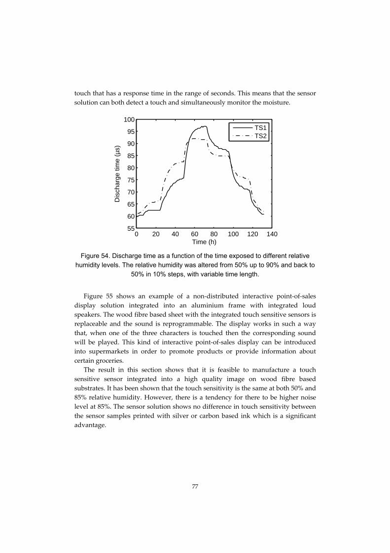
touch that has a response time in the range of seconds. This means that the sensor
solution can both detect a touch and simultaneously monitor the moisture.
0 20 40 60 80 100 120 14055
60
65
70
75
80
85
90
95
100 TS1TS2
Time (h)
Dis
char
ge ti
me
(µs)
Figure 54. Discharge time as a function of the time exposed to different relative humidity levels. The relative humidity was altered from 50% up to 90% and back to
50% in 10% steps, with variable time length.
Figure 55 shows an example of a non‐distributed interactive point‐of‐sales
display solution integrated into an aluminium frame with integrated loud
speakers. The wood fibre based sheet with the integrated touch sensitive sensors is
replaceable and the sound is reprogrammable. The display works in such a way
that, when one of the three characters is touched then the corresponding sound
will be played. This kind of interactive point‐of‐sales display can be introduced
into supermarkets in order to promote products or provide information about
certain groceries.
The result in this section shows that it is feasible to manufacture a touch
sensitive sensor integrated into a high quality image on wood fibre based
substrates. It has been shown that the touch sensitivity is the same at both 50% and
85% relative humidity. However, there is a tendency for there to be higher noise
level at 85%. The sensor solution shows no difference in touch sensitivity between
the sensor samples printed with silver or carbon based ink which is a significant
advantage.
77

Figure 55. Example of a non-distributed interactive point-of-sales display solution with integrated loud speakers
78
5 SUMMARY OF PUBLICATIONS
The nine papers in this thesis deal with low cost sensors, some printable and
others which are applications of low cost commercial tags. System integration of a
hybrid BAP RFID based sensor system.
5.1 Paper I
The performance of a capacitive printed touch sensitive sensor is investigated
and compared to other commercially available touch screens. The advantage
associated with the proposed sensor solution is that it is a low cost sensor that can
be integrated into a high quality print. The targeted applications are large area
touch sensitive commercial stands, flat keyboards at the point of purchase and
touch and manipulation surveillance in logistic chains. The study also compared
different kinds of communication links between the readout electronic circuit and
external devices, from high‐end wireless systems that are utilizing RFID or ZigBee
to simple analogue wire solutions.
5.2 Paper II
This work presents a study related to the performance of printed low cost
moisture sensors fabricated using conductive ink on paper substrates. The sensors
are intended to add value to the surveillance of packages. Two different kinds of
sensors are evaluated and characterized. The two sensors have similar geometrical
shapes, but different measuring principles are employed. The first sensor measures
the moisture content in cellulose based substrates, while the second measures the
high levels of relative humidity in the surroundings. The sensors have been
developed so that they can be integrated into Radio Frequency Identification
(RFID) systems for surveillance in logistic chains. A laboratory set‐up of a RFID tag
with sensor capability based on an ordinary passive RFID tag has been shown.
5.3 Paper III
In this work a two‐chip battery assisted Radio Frequency Identification (RFID)
based sensor platform is presented. The radio frequency communication interface
is based on the EPC Gen 2 standard. A laboratory set‐up of the platform has been
shown and characterized for a moisture content sensor application. The laboratory
set‐up of the sensor platform has a reading range of 3.4 meters which is in
comparison to commercially available Gen 2 tags. The laboratory platform has an
average power consumption of 2.1 μW operating at 3 V, which together with a
printed battery gives an estimated lifetime for data logging of several years.
79
80
The proposed RFID platform provides a trade‐off between, communication
performance, compatibility with international standards and flexibility in on‐
package customization including type and number of sensors. The proposed
architecture separates the high performance communication circuit and the low
frequency sensor interface logic. In the future the sensor interface may be
integrated using printed logics to further enhance the flexibility and low cost
customization features of the architecture.
5.4 Paper IV
In this work the two‐chip battery assisted passive RFID based sensor platform
presented in Paper III is evaluated for two different packaging surveillance
applications. The results show that the sensor platform can easily be tailored to be
used with different types of sensors to achieve the desired solution, such as, shock,
tilt and tamper evidence sensors and detectors. For a tilt sensor solution the sensor
platform can have a battery lifetime above 3 years when being powered by a
battery with an energy capacity of 33 mAh.
5.5 Paper V
In this work the design and manufacturing of an inkjet printed resistive type
humidity sensor on paper is reported. After having been exposed to humidity
above a threshold level the resistance of the sensor decreases substantially and
remains at that level when humidity is reduced. This sensor can be used in various
applications for environmental monitoring where the memory effect means that
the highest humidity exposure is recorded. The humidity level can be deducted by
monitoring the rate of change. A possible cause for this behaviour is the presence
of polyvinylpyrrolidone (PVP) which can enable ionic transport within the
polymer when exposed to humidity. The simple manufacturing procedure makes
it a good and versatile low cost sensor solution that can be integrated with printed
flexible electronics.
5.6 Paper VI
A horizontal printed Write Once Read Many (WORM) resistive memory has
been developed for use in wireless sensor tags targeting single event detection in
smart packaging applications. The WORM memory can be programmed using a
1.5 V printed battery. An alternative programming method is to use chemical
sintering which allows the development of exposure time triggered single event
tags that can be accessed wirelessly. The new WORM memory has very low losses
in the ON‐state which allows direct integration into RF antenna structures. A
sensor tag architecture that utilizes the WORM memory functionality and the well

established Electronic Article Surveillance (EAS) communication standard has
been outlined. Both active (printed battery powered) and fully passive sensor tag
solutions have been proposed. The role of printed electronics in smart packaging
applications has been reviewed and discussed. Important enabling factors for the
future development have been highlighted, such as the need for hierarchical
design and test tools, better printed interconnect technologies as well as better
components that allow communication with existing information and
communication technology (ICT) standards. This is illustrated and underlined by
the presented smart packaging concept demonstrators. Finally, we conclude that
the new horizontal WORM memory technology provides an important additional
tool to reach future fully printed smart packaging wireless communication
platforms. The ongoing research on resistive memory structures with multiple read
and write functionality could further advance such technology platforms.
5.7 Paper VII
A simple printable moisture sensor that is based on a carbon‐zinc type energy
cell is characterized. The energy cell based sensor provides power to a readout
electronic circuit when activated by moisture. Typical applications are moisture
and leakage detection in buildings, water pipe lines, smart packages and health
care systems. In the study some critical parameters are characterized such as
power driving capability and internal memory effects. In addition a specific
application for the surveillance of frozen articles during transport is examined.
5.8 Paper VIII
The paper presents a concept where pairs of ordinary RFID tags are exploited
for use as remotely read moisture sensors. The pair of tags is incorporated into one
label where one of the tags is embedded in a moisture absorbent material and the
other is left open. In a humid environment the moisture concentration is higher in
the absorbent material than in the surrounding environment which causes
degradation to the embedded tag’s antenna in terms of dielectric losses and change
of input impedance. The amount of water in the absorbent material is determined
for a passive RFID system by comparing the difference in the RFID reader output
power required to power up the open and embedded tag, respectively. It is
similarly shown how the backscattered signal strength for a semi‐active RFID
system is proportional to the amount of water in the absorbent material. Typical
applications include moisture detection in buildings, especially from leaking water
pipe connections hidden within walls. The presented solution has a cost that is
comparable to ordinary RFID tags. The passive system also has infinite life‐time
since no internal power supply is needed. The concept is characterized for two
81
commercial RFID systems, one passive operating at 868 MHz and one semi‐active
operating at 2.45 GHz.
5.9 Paper IX
The paper presents a review in relation to existing system integration
technologies relevant for smart packaging applications. The objective is to
summarize and to outline possible future technology directions for system
integration of electronic functionalities in paper based packaging solutions. Recent
advances in printed electronics, RFID tag production and standardization of
communication protocols are factors that increase the design freedom for new
applications. As in all new technology fields the first products are expected to
appear in the high cost segment attracting early adopters in the form of niche
products. A reasonable assumption is that these products will come from
hybridization of different types of technologies. Such a scenario is likely since no
technology solution available can provide all the features that these types of
applications demand.
There is a requirement for standard solutions for the hybridization of silicon
devices and printed (or foil type) components. Conductive ink technology is a
powerful tool for hybridization and customization of large area electronics
providing 3D integration and large area customization. However, high
performance communication and advanced processing demands the use of silicon.
Smart hybridization solutions allow for a combination of the best from both
worlds.
This work provides a technology review and an analysis of the requirements for
a hybridization technology suitable for smart packaging applications. To illustrate
the concepts discussed we also present design examples on intrusion surveillance
solutions for cellulose based packaging applications.
5.10 Author’s contributions
The contribution of the author of this thesis has been essential to all the papers
listed in Table 22.
82
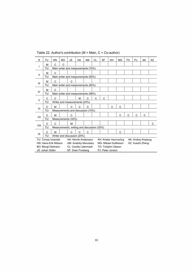
Table 22. Author's contribution (M = Main, C = Co-author)
# TU HN BO JS HA AM CL SF KH MG TO PJ AK XZ
M C C I
TU: Main writer and measurements (70%)
M C II
TU: Main writer and measurements (95%)
M C C III
TU: Main writer and measurements (90%)
M C IV
TU: Main writer and measurements (98%)
C C M C C C V
TU: Writer and measurements (24%)
C M C C C C C VI
TU: Measurements and discussion (10%)
C M C C C C C VII
TU: Measurements (32%)
C C M C VIII
TU: Measurements, writing and discussion (30%)
C M C C C C IX
TU: Writer and discussion (20%)
TU: Tomas Unander HN: Hans-Erik Nilsson BO: Bengt Oelmann JS: Johan Sidén
HA: Henrik Andersson AM: Anatoliy Manuilskiy CL: Cecilia Lidenmark SF: Sven Forsberg
KH: Krister Hammarling MG: Mikael Gulliksson TO: Torbjörn Olsson PJ: Peter Jonson
AK: Andrey Koptyug XZ: Xuezhi Zheng
83


85
6 THESIS SUMMARY AND CONCLUSIONS
The design and characterization of a battery assisted passive RFID sensor
platform together with the fabrication and characterization of printed low cost
sensors have been presented in this thesis. An introduction to the research area has
been provided in section 1. In section 2 the BAP RFID sensor platform is presented
and evaluated for three smart packaging applications. In section 3 six different
moisture sensor solutions are presented. Some of these are printed whilst others
utilize ordinary commercial available systems to give moisture sensing features.
The moisture sensor solutions are targeting applications such as the moisture
monitoring of wood fibre based packages, moisture and leakage detection in
buildings and health care systems.
In section 4 a printed touch sensitive sensor solution has been presented. The
targeted applications for the touch sensitive sensor solution are large area touch
sensitive commercial stands, flat keyboards at the point of purchase and touch and
manipulation surveillance in logistic chains. Section 5 gives a brief summary of the
original papers that this thesis is based on.
The low cost sensor solutions evaluated show a good correlation to the targeted
specification set by the applications. In the following sections a more detailed
summary and conclusion for the different sensor solutions are presented.
6.1 BAP RFID based sensor system
In section 2 a battery assisted passive RFID sensor system is presented. The
proposed RFID platform provides a trade‐off between, communication
performance, compatibility with international standards and flexibility in on‐
package customization including type and number of sensors. The proposed
architecture separates the high performance communication circuit and the low
frequency sensor interface logic. In the future the sensor interface maybe
integrated using printed logics to further enhance the flexibility and low cost
customization features of the architecture.
Smart packing applications demand large volumes, and low cost production as
well as low cost customization for each product. A trade‐off between all these
demands is necessary in order to obtain a competitive technology platform. The
proposed structure has the advantage of providing the required communication
performance and the design flexibility for the specific application. The forecast in
relation to printed electronics indicates that low frequency digital circuits (sensor
interfaces) are ready for large scale commercialization within the foreseeable future
[26, 140]. Such technology could very well replace the sensor chip in our platform
and thus provide low cost customization solutions with high performance
communication by the silicon RFID Gen 2 chip.
The study show that it is possible to manufacture a laboratory RFID based
sensor platform with a reading range within the same range as a commercially
available Gen 2 tag. The laboratory set‐up of the sensor platform has been shown
to be readily tailored to work with different types of sensors.
6.2 Printed moisture content sensor for wood fibre based substrates
In section 3.1 a printed moisture content sensor has been presented. The sensor
solution is based on the same capacitive sensor concept as the touch sensitive
sensor solution presented in section 4, but, in this case, the effect of the moisture
dependency is characterized.
The result shows a good correlation between the sensor response and the
moisture content in cellulose based substrates. The evaluated sensor solution has a
measuring accuracy with a coefficient of variance of 0.22% and a temperature
difference of 0.36%. A laboratory set‐up of a two chip semi‐passive RFID tag with
moisture content sensing features has also been presented.
6.3 Printed relative humidity sensor for high relative humidity levels
In section 3.2 a relative humidity sensor has been presented. The sensor
solution is based on a resistive measuring technique that measures the DC current
through a sensor. The DC current is determined by measuring the voltage over a
resistor in series with the sensor two seconds after a 0 to 1.55 V transition.
The experimental results show that in order to manufacture as good a sensor as
possible the sensor should be manufactured with a highly conductive material and
the line spacing between the electrodes in the two‐dimensional structure (Figure
18) should be as short as possible to increase the DC current through the sensor.
6.4 Printed action activated moisture sensor
In section 3.3 a printed action activated moisture sensor has been presented.
The sensor is based on an energy cell that provides power when activated by
moisture.
The result shows that the concept of using carbon‐zinc energy cells as an action
activated moisture sensor is feasible. It also shows that the sensor can be
manufactured with different trigger and signal levels to be optimized towards
specific applications. The sensor can utilize the hysteresis effect of hygroscopic
materials, such as cellulose based paper, to provide a stable triggering signal. A
defrosting alarm for the monitoring of frozen articles has been presented. The
sensor is triggered after approximately a minute or less after the sensor
86
temperature rises above zero degrees centigrade. By stacking four energy cells in
series it is possible to power up and program the RFID based sensor platform
presented in section 2.
6.5 Remote moisture sensing utilizing ordinary RFID tags
In section 3.4 a remote moisture sensor that utilizes ordinary RFID tags has
been presented. The concept is based on an idea in which a pair of RFID tags is
used, where one is embedded in a moisture absorbing material while the other
remains open. The power difference required to power up the tags is used to
determine the humidity in the moisture absorbing material.
The results show that the concept with remote moisture sensing using ordinary
RFID tags is feasible. The difference in power levels for the different levels of
relative humidity proved to be of the order of approximately two to three decibels
for the 80% relative humidity and it is possible that this humidity level might
prove to be the starting point for the source of mould. The hysteresis effect of
paper materials could be the source of a problem since it may make incorrect
readings due to memory effects. However, an incorrect reading due to hysteresis
still indicates that the humidity level has been high.
6.6 Printed nano-particle based sensor moisture sensors
In section 3.5 an initial study on a printed nano‐particle based relative humidity
sensor has been presented. In the study two different types of sensor structures are
investigated, one being a horizontal single layer structure for high humidity levels
and the other being a two‐layer structure for very dry moisture conditions. The
printed single layer solution utilizes short and narrow lines of silver nano‐particles
for humidity detection. The two‐layer solution utilizes an effect in unsintered silver
nano‐particles to measure the relative humidity in the surroundings. The
measurements in both of the solutions are conducted by measuring of the DC
resistance in the printed nano‐particle based sensors.
The result shows that it is possible to manufacture printed moisture sensors
with silver nano‐particles. For the two‐layer relative humidity sensor for very low
humidity levels 75% of the samples had a variance of 8% without calibration of the
single samples. The sensor solution shows a linear response as the relative
humidity is increased from 10% to 50%. However, the sensor shows a hysteresis
effect when the relative humidity is again reduced down to 10%.
6.7 Printed touch sensitive sensor
In section 4 a printed touch sensitive sensor has been presented. The concept of
the sensor solution is to incorporate a touch sensitive sensor into a high quality
87
image. The sensor solution is based on a capacitive measuring technique. The
building blocks of the sensor solution are presented with the printed sensor
structure, the readout electronics and the communication interface.
The result shows that it is feasible to manufacture a touch sensitive sensor
integrated into a high quality image on cellulose based substrates. It has been
shown that the touch sensitivity is the same at 50% as 85% relative humidity.
However, there is a tendency towards higher noise level at 85%. The sensor
solution shows no difference in touch sensitivity between sensor samples printed
with silver or carbon based ink.
6.8 Conclusions
The work in this thesis has shown the possibility associated with combining
printed large area components, such as, antenna, sensor and interface, with
traditional silicon based electronics in order to achieve a two‐chip BAP RFID based
sensor platform directly on wood fibre based substrates. A theoretically long
battery lifetime of the platform has also been shown by using commercially
available printed batteries. The thesis also show the possibility to, with printed
means, create moisture sensing features on wood fibre based substrates, such as,
moisture content sensor, relative humidity sensor and AAT sensor. Concepts,
using commercially available RFID tags, in order to create moisture sensitive
sensors that can be read remotely, have also been discussed.
88

REFERENCES
[1] N. Wang, N. Zhang, M. Wang, Wireless sensors in agriculture and food
industry ‐ Recent development and future perspective, Computers and
Electronics in Agriculture, vol. 50, No. 1, pp. 1‐14, 2006
[2] Interpack, [Online], Available: http://www.interpack.com
[3] IDTechEx, [Online], Available: http://www.idtechex.com
[4] Denso Wave Inc. – About QR codes, [Online], Available: http://www.denso‐
wave.com/qrcode/index‐e.html
[5] Apple – QR code creation for address exchange, [Online], Available:
http://www.apple.com/webapps/utilities/qrcodecreationforaddressexchange
.html
[6] Upcode Ltd., [Online], Available: http://www.upc.fi/en/upcode
[7] PolyIC, [Online], Available: http://www.polyic.com
[8] Infineon Technologies AG, [Online], Available: http://www.infineon.com
[9] Ntera Inc., [Online], Available: http://www.ntera.com
[10] Electro Luminescence Inc., [Online], Available: http://electroluminescence‐
inc.com
[11] Add‐Vision Inc., [Online], Available: http://www.add‐vision.com
[12] E Ink Corp., [Online], Available: http://www.eink.com
[13] SiPix Imaging, Inc., [Online], Available: http://www.sipix.com
[14] Liquavista, [Online], Available: http://www.liquavista.com
[15] Kovio Inc., [Online], Available: http://www.kovio.com
[16] ThinFilm Electronics, [Online], Available: http://thinfilm.se
[17] Eight19, [Online], Available: http://www.eight19.com
[18] Blue Spark ST Battery Series, [Online], Available:
http://www.bluesparktechnologies.com/pdf/Blue_Spark_ST_Series_Batteries
_09‐10‐1.pdf
[19] Enfucell Technical Specifications for SoftBattery, [Online], Available:
http://www.enfucell.com/softbattery_specifications.pdf
[20] A. Pacquit, J. Frisby, D. Diamond, K. T. Lau, A. Farrell, B. Quilty and D.
Diamond, Development of a smart packaging for the monitoring of fish
spoilage, Food Chemistry, vol. 102, No. 2, pp. 466‐470, 2007
[21] N. P. Mahalik and A. N. Nambiar, Trends in food packaging and
manufacturing systems and technology, Trends in food science &
technology, vol. 21, no. 3, pp. 117‐128, 2010
[22] BRIDGE, EU FP6 Programme, WP13 European Passive RFID Market Sizing
2007‐2022, [Online], Available: http://www.bridge‐
project.eu/data/File/BRIDGE%20WP13%20European%20passive%20RFID%2
0Market%20Sizing%202007‐2022.pdf
89
90
[23] UHF Class 1 Gen 2 Standard v. 1.2.0, [Online], Available:
http://www.gs1.org/sites/default/files/docs/uhfc1g2/uhfc1g2_1_2_0‐
standard‐20080511.pdf
[24] ISO/IEC 18000‐6C air interface protocol, [Online], Available:
http://www.iso.org/iso/iso_catalogue/catalogue_tc/catalogue_detail.htm?csn
umber=34117
[25] Y.‐C. Hsu, A.‐P. Chen, C.‐H. Wang, “A RFID‐Enabled Traceability System
for the Supply Chain of Live Fish”, Proceedings of the IEEE International
Conference on Automation and Logistics, Qingdao, China, September 2008,
pp. 81‐86
[26] M. Jung, J. Kim, J. Noh, N. Lim, C. Lim, G. Lee, J. Kim, H. Kang, K. Jung, A.
D. Leonard, J. M. Tour and G. Cho, “All‐Printed and Roll‐to‐Roll‐Printable
13.56‐MHz‐Operated 1‐bit RF Tag on Plastic Foils”, IEEE Transactions on
Electron Devices, vol. 57, no. 3, pp. 571‐580, March 2010
[27] V. Subramanian, J. B. Chang, A. Vornbrock, D. C. Huang, L. Jagannathan, F.
Liao, B. Mattis, S. Molesa, D. R. Redinger, D. Soltman, S. K. Volkman, Q.
Zhang, Printed electronics for low‐cost electronic systems: Technology status
and application development, Proceedings of the 38th European Solid‐State
Device Research Conference, ESSDERC, 2008, pp. 17‐24
[28] The Confederation of Paper Industries, [Online], Available:
http://www.paper.org.uk
[29] S. Simula, K. Niskanen, “Electrical Properties of viscose‐kraft fibre
mixtures,” in Nordic Pulp and Paper Research Journal, vol. 14, no. 3, pp.
243‐246, 1999
[30] E. J. Murphy, “The Dependence of the Conductivity of Cellulose, Silk and
Wool on Their Water Content”, Journal of Physics and Chemistry Solids, vol.
16, issues 1‐2, Nov 1960, pp 115‐122
[31] A. Rida, L. Yang, R. Vyas and M. M. Tentzeris, “Conductive Inkjet‐Printed
Antennas on Flexible Low‐Cost Paper‐Based Substrates for RFID and WSN
Applications”, IEEE Antennas and propagation magazine Vol. 51, No. 3, pp.
13‐23, 2009
[32] A. C. Siegel, S. T. Phillips, M. D. Dickey, N. Lu, Z. Suo and G. M. Whiteside,
“Foldable Printed Circuit Boards on Paper Substrates”, Advanced
Functional Materials, Vol. 20, No. 1, pp. 28‐35, 2010
[33] T. Uesaka, “Dimensional Stability and Environmental Effects of Paper
Properties,” in Handbook of Physical Testing of Paper, 2nd ed. vol. 1, R.E.
Mark, New York: Marcel Dekker, 2002, pp. 115‐171
[34] R. E. Benson, “Effects of relative humidity and temperature on tensile stress‐
strain properties of kraft linerboard,” Tappi 54(4), 1971, pp 699‐703
[35] A.‐L. Pasanen, J.‐P. Kasanen, S. Rautiala, M. Ikäheimo, J. Rantamäki, H.
Kääriäinen, P. Kalliokoski, “Fungal growth and survival in building
materials under fluctuating moisture and temperature conditions”,
International Biodeterioration & Biodegradation, vol. 46, issue 2, September
2000, pp. 117‐127
[36] T. A. Shimp, “Advertising, Promotion: Supplemental Aspects of Integrated
Marketing Communications,” 5th ed., Fort Worth, USA: Dryden Press, 2000
[37] Presentation of EM4325 RFID chip (under development), [Online],
Available:
http://www.stech.cz/download.php?id_document=401158198&at=1
[38] Product selection table for EM Microelectronic‐Marin SAs RFID ICs,
[Online] , Available:
http://www.emmicroelectronic.com/webfiles/product/RFID/RFIDprodtab.pd
f
[39] EM Microelectronic‐Marin SA, [Online], Available:
http://www.emmicroelectronic.com
[40] SL900A data sheet, [Online], Available: http://www.ids‐
microchip.com/doc/sd/SL900A_SD.pdf
[41] WM72016 data sheet, [Online], Available:
http://www.ramtron.com/files/datasheets/WM72016_ds.pdf
[42] PIC18LF13K22 data sheet, [Online], Available:
http://ww1.microchip.com/downloads/en/DeviceDoc/41365D.pdf
[43] Microchip, Technology Inc., [Online], Available: http://www.microchip.com
[44] D. K. Cheng, “Field and Wave Electromagnetics”, 2nd ed., ISBN 0‐201‐
12819‐5, pp 400, 461, and 489, Addison Wesley, UK, 1989
[45] J. Sidén, H.‐E. Nilsson, “Line Width Limitations of Flexographic‐ Screen‐ and
Inkjet printed RFID Antennas”, Proceedings of IEEE AP‐S, pp 1745‐1748,
2007
[46] W. L. Stutzman, G. A. Thiele, ”Antenna Theory and Design”, 2nd ed., pp
170, ISBN 0‐471‐02590‐9, John Wiley & Sons, 1998
[47] D. M. Dobkin, “The RF in RFID: Passive UHF RFID in Practice”, pp 321‐323,
ISBN 978‐0750682091, Newnes, 2008
[48] N. Cho, S.‐J. Song, J.‐Y. Lee, S. Kim, S. Kim, H.‐J. Yoo, “A 8‐μW, 0.3‐mm2 RF‐
Powered Transponder with Temperature Sensor for Wireless Environmental
Monitoring”, IEEE International Symposium on Circuits and Systems
(ISCAS 2005), 23‐26 May 2005, Kobe, Japan, pp 4763‐4766
[49] N. Cho, S.‐J. Song, J.‐Y. Lee, S. Kim, S. Kim, H.‐J. Yoo, “A 5.1‐μW UHF RFID
Tag Chip integrated with Sensors for Wireless Environmental Monitoring”,
Proceedings of ESSCIRC, Grenoble, France, 2005, pp 279‐282
91

[50] A. P. Sample, D. J. Yeager, P. S. Powledge, J. R. Smith, “Design of a
Passively‐Powered, Programmable Sensing Platform for UHF RFID
Systems”, IEEE International Conference on RFID, 26‐28 March 2007,
Grapevine, TX, USA, pp 149‐156
[51] D. J. Yeager, P. S. Powledge, R. Prasad, D. Wetherall, J. R. Smith,
“Wirelessly‐Charged UHF Tags for Sensor Data Collection”, IEEE
International Conference on RFID, April 16‐17, 2008, Las Vegas, NV, USA,
pp 320‐327
[52] 3V lithium battery technical overview, [Online], Available:
http://www.renata.com/content/3vlithium/overview.php
[53] Food Standards Australia New Zealand, Food Safety: Temperature control
of potentially hazardous foods, [Online], Available:
http://www.foodstandards.gov.au/_srcfiles/FSTemp_control_Edition_for_pri
nting.pdf
[54] EMDB412 fact sheet, [Online] , Available:
http://www.emmicroelectronic.com/webfiles/product/rfid/ds/EMDB412_FS.
[55] SkyeModule M9, [Online], Available:
http://www.skyetek.com/Portals/0/Documents/Products/SkyeModule_M9_D
ataSheet.pdf
[56] SkyeTek, [Online], Available: http://www.skyetek.com
[57] UHF broadband antenna fact sheet, [Online], Available:
http://www.skyetek.com/LinkClick.aspx?link=Documents/Products/SkyeTek
_Broadband_UHF_Antenna_Datasheet.pdf&tabid=417.
[58] P. Oittinen, H. Saarelma, “Mechanical Printing,” in Papermaking Science
and Technology, vol. 13, P. Oittinen, H. Saarelma, Helsinki, Finland: Fapet
Oy, 1998, pp. 133‐170
[59] Coates Screen, [Online], Available: http://www.coates.com
[60] MACtac, [Online], Available: http://www.mactac.com
[61] A. Kiviranta, “Paperboard grades,” in Papermaking Science and
Technology, vol. 18, H. Paulapuro, Helsinki, Finland: Fapet Oy, 2000, pp. 54‐
72
[62] Mettler Toledo, [Online], Available: http://www.mettler‐toledo.com
[63] C. Nordling, J. Österman, “Physics handbook for science and engineering”,
6th ed., ISBN: 91‐44‐00823‐6, Studentlitteratur, Lund
[64] Ramarao V. Bandaru, Professor & Associate Director, Department of Paper
& BioProcess Engineering, Empire State Paper Research Institute, State
University of New York College of Environmental Science & Forestry,
private communication, 2009
92

[65] ShockWatch Impact Indicators, [Online], Available:
http://www.shockwatch.com/pdfs/ds_impact_indicators.pdf.
[66] MMA7260Q three axis low‐g micromachined Accelerometer data sheet,
[Online], Available:
http://www.freescale.com/files/sensors/doc/data_sheet/MMA7260QT.pdf
[67] ShockWatch Tilt Indicators, [Online], Available:
http://www.shockwatch.com/pdfs/ds_tilt_indicators.pdf
[68] Security tape & tamper evident tape from Tamper Evident, [Online],
Available: http://www.tamperevident.com.au/tape_seals_page.php
[69] XOLAR solar bits, [Online], Available:
http://www.farnell.com/datasheets/578090.pdf
[70] IXYS Corporation, [Online], Available: http://www.ixys.com
[71] S. Folea, M. Ghercioiu, ”Ultra‐low power Wi‐Fi tag for wireless sensing”,
Proc. of IEEE Int. Conf. on Automation, Quality and Testing, Robotics, vol.
03, 2008, pp 247‐252
[72] V. Mattoli, B. Mazzolai, A. Mondini, S. Zampolli, P. Dario, “Flexible tag for
datalogger for food logistics”, Sens. Actuators A: Phys. 2010,
doi:10.1016/j.sna.2010.01.028
[73] M. Baghaei‐Nejad, D. S. Mendoza, Z. Zou, S. Radiom, G. Gielen, L.‐R.
Zheng, H. Tenhunen, “A remote‐powered RFID tag with 10Mb/s UWB
uplink and ‐18.5dBm sensitivity UHF downlink in 0.18μm CMOS”, 2009
IEEE Int. Solid‐State Circuits Conference (ISSCC’09), San Francisco, USA,
Feb. 2009, pp 198‐199
[74] Hongwei Shen; Lilan Li; Yumei Zhou, ʺFully integrated passive UHF RFID
tag with temperature sensor for environment monitoring,ʺ, ASICON ʹ07 7th
International Conference on ASIC, Guilin 22‐25 Oct. 2007, pp.360‐363
[75] I. Kajanto, K. Niskanen, “Dimensional Stability,” in Papermaking Science
and Technology, vol. 16, K. Niskanen, Helsinki, Finland: Fapet Oy, 2000, pp.
223‐259
[76] D. E. Gunderson, “A method for compressive creep testing of paperboard,”
Tappi 64(11), 1981, pp 67‐71.
[77] K. Hartikainen, “Corrugated board manufacturing,” in Papermaking Science
and Technology, vol. 12, A. Savolainen, Helsinki, Finland: Fapet Oy, 1998,
pp. 244‐269
[78] P. R. Story, D. W. Galipeau, R. D. Mileham , “A study of low‐cost sensors for
measuring low relative humidity”, Sensors and Actuators B: Chemical, vol.
25, issues 1‐3, April 1995, pp. 681‐685
[79] P. M. Harrey, B. J. Ramsey, P. S. A. Evans, D. J. Harrison, “Capacitive‐type
humidity sensors fabricated using the offset lithographic printing process”,
93
Sensors and Actuators B: Chemical, vol. 87, issue 2, 10 December 2002, pp.
226‐232
[80] J. Wang, X.‐H. Wang, X.‐D. Wang, “Study on dielectric properties of
humidity sensing nanometer materials”, Sensors and Actuators B: Chemical,
vol. 108, issues 1‐2, 22 July 2005, pp. 445‐449
[81] P. Norberg, “Microclimate Measurements in the Built Environment,” KTH,
Centre for Built Environment, ISBN 91‐7170‐341‐1, 1998.
[82] Norwegian Institute for Air Research, [Online], Available:
http://www.nilu.com
[83] R. S. Jachowicz, K. Kulpa, “A Thin‐Film Capacitive Humidity Sensor,”
Sensors and Actuators, no. 2, 1981/1982, pp. 171‐186
[84] Data sheet HP Advanced photo paper Q5456A, [Online], Available:
http://h20195.www2.hp.com/v2/GetPDF.aspx/4AA0‐6819EEE.pdf
[85] Xerox Corporation, [Online], Available: http://www.xerox.com
[86] P. Oittinen, H. Saarelma, “Electronic Printing,” in Papermaking Science and
Technology, vol. 13, P. Oittinen, H. Saarelma, Helsinki, Finland: Fapet Oy,
1998, pp. 173‐191
[87] Cabot Corporation, [Online], Available: http://www.cabot‐corp.com
[88] Jetrion LLC, [Online], Available: http://www.jetrion.com
[89] A. Oprea, N. Bârsan, U. Weimar, M.‐L. Bauersfeld, D. Ebling, J. Völlenstein,
“Capacitive humidity sensors on flexible RFID labels”, Sensors and
Actuators B: Chemical, Vol. 132, issue 2, 16 June 2008, Pages 404‐410
[90] J. Sidén, A. Koptioug, M. Gulliksson, “The “Smart” Diaper Moisture
Detection System”, Microwave Symposium Digest, 2004 IEEE MTT‐S
International, vol. 2, 6‐11 June 2004, pp. 659 – 622
[91] Extech Instruments Corp., [Online], http://www.extech.com
[92] Alfasensor AB, [Online], Available: http://www.alfasensor.com
[93] Multisorb Technologies Inc., [Online], Available: http://www.multisorb.com
[94] Levosil S.p.A., [Online], Available: http://www.levosil.com
[95] Süd‐Chemie AG, [Online], Available: http://www.sud‐chemie.com
[96] M. S. Park, S. H. Hyun, S. C, Nam, ”Characterization of a LiCo02 thick film
by screen‐printing for a lithium ion micro‐battery”, Journal of Power
Sources, vol. 159, issue 2, September 2006, pp. 1416‐1421
[97] J. Huand, J. Yang, W. Li, W. Cai, Z. Jiang, ”Electrochemical properties of
LiCoO2 thin film electrode prepared by ink‐jet printing technique”, Thin
Solid Films, vol. 516, issue 10, March 2008, pp. 3314‐3319
[98] W. G. Tam, J. S. Wainright, “A microfabricated nickel‐hydrogen battery
using thick film printing techniques”, Journal of Power Sources, vol. 165,
issue 1, February 2007, pp. 481‐488
94
[99] J.‐S. Do, S.‐H. Yu, S.‐F. Cheng, “Thick‐film nickel‐metal‐hydride battery
based on porous ceramic substrates”, Journal of Power Sources, vol. 117,
issue 1‐2, May 2003, pp. 203‐211
[100] D. Southee, G. I. Hay, P. S. A. Evans, D. J. Harrison, “Development and
Characterization of Lithographically Printed Voltaic Cells”, Electronics
Systemintegration Technology Conference, 2006, vol. 2, Sept. 2006, pp.1286‐
1291
[101] Power Paper Ltd. [Online], Available: http://www.powerpaper.com
[102] Z. Wei, W. Hauyng, S. Zhang, J. Tan, “Carbon‐based air electrodes carrying
MnO2 in zinc‐air batteries”, Journal of Power Sources, vol. 91, issue 2,
December 2000, pp. 83‐85
[103] Keithley 2410 high voltage sourcemeter data sheet, [Online], Available:
http://www.keithley.com/data?asset=372
[104] W. Brecht, “Beating and hygrostability of paper,” in Fundamentals of
papermaking fibres, vol 1, F. Bolam, London, United Kingdom: Tech. Sect.
British Paper and Board Makers Assoc., 1958, pp. 241
[105] F. Menke, R. Knochel, T. Boltze, C. Hauenschild, W. Leschnik, “Moisture
measurement in walls using microwaves”, Microwave Symposium Digest,
vol. 3, 16‐20 May 1995, pp. 1147‐1150
[106] T. Hauschild, F. Menke, “Moisture measurement in masonry walls using a
non‐invasive reflectometer”, Electronics Letters, vol. 34, issue 25, 10 Dec.
1998, pp. 2413‐2414
[107] L. Reindl, C.C.W. Ruppel, A. Kirmayr, M. Stockhausen, M.A. Hilhorst, J.
Balendonck, “Radio‐requestable passive SAW water‐content sensor”,
Microwave Theory and Techniques, IEEE Transactions on Microwave
Theory and Techniques, vol. 49, issue 4, Part 2, April 2001, pp. 803‐808
[108] T. J. Harpster, B. Stark, K. Najafi, “A passive wireless integrated humidity
sensor”, Sensors and Actuators A: Physical, vol. 95, issues 2‐3, 1 January
2002, pp. 100‐107
[109] MicroDAQ.com Ltd., [Online], Available: http://www.microdaq.com
[110] Alien Technology Corp., [Online], Available:
http://www.alientechnology.com
[111] TagMaster, [Online], Available: http://www.tagmaster.se
[112] SCA Luna core, [Online], Available:
http://www.sca.com/en/pulp/Products1/Luna1/Luna‐Grades/Luna‐Core
[113] Kapton polyimide film, [Online], Available:
http://www2.dupont.com/Kapton/en_US/
[114] Summary of properties for Kapton polyimide films, [Online], Available,
http://www2.dupont.com/Kapton/en_US/assets/downloads/pdf/summaryof
prop.pdf
95

[115] A. Alastalo, T, H. Seppä, J. H. Leppäniemi, M. Aronniemi, J, M. L. Allen, and
T. Mattila, “Modelling of Nanoparticle Sintering under Electrical boundary
Conditions”, J. Phys. D:Appl. Phys., vol. 43, no.48, 2010
[116] M. L. Allen, M. Aronniemi, T. Mattila, A. Alastalo, K. Ojanpera, M. Suhonen,
and H. Seppä, “Electrical Sintering of Nanoparticle structures”,
Nanotechnology, vol. 19, pp. 175201‐1‐4, 2008
[117] J. H. Leppäniemi, M. Aronniemi, T. Mattila, A. Alastalo, M. L. Allen, and H.
Seppä,” Printed WORM Memory on Flexible Substrate Based on Rapid
Electrical Sintering of Nanoparticles”, Trans. Electron Devices, in press,
2010
[118] J. R. Greer and R. A. Street, “Thermal cure effects on electrical performance
of nanoparticle silver inks”, Acta. Mater., vol. 55, pp. 6345‐6349, 2007
[119] S. Magdassi, M. Grouchko, O. Berezin, and A. Kamyshny, “Triggering the
Sintering of Silver Nanoparticles at Room Temperature”, ACS Nano, vol. 4,
pp. 1943‐1948, Apr 2010
[120] W. Zapka, W. Voit, C. Loderer, and P. Lang, “Low temperature chemical
post‐treatment of inkjet printed nano‐particle silver inks”, Proc. NIP 24:
Digital Fabrication, Pittsburgh, USA, Sept. 2008, pp. 906‐11
[121] Information on silverjet DGP 40LT‐15C, [Online, Available:
http://www.anapro.com/english/product/nano_silver.asp
[122] Advanced Nano Products Co.,Ltd., [Online], Available:
http://www.anapro.com/english/
[123] SD Association, [Online], Available: http://www.sdcard.org
[124] Fujifilm Dimatix DMP‐2831 data sheet, [Online], Available:
http://www.dimatix.com/files/DMP‐2831‐Datasheet.pdf
[125] Canon photo paper pro platinum (PT‐101) technology guide, [Online],
Available: http://www.usa.canon.com/app/pdf/printer/PT101_Guide.pdf
[126] H. Wang, X. Qiao, J. Chen, X. Wang, and S. Ding, “Mechanisms of PVP in
the preparation of silver nanoparticles”, Mater. Chem. Phys. vol. 94, pp.449‐
453, 2005
[127] K. Ogura, A. Fujii, H. Shiigi, M. Nakayama, and T. Tonosaki, “Effect of
hygroscopicity of insulating unit of polymer composites on their response to
relative humidity”, J. Electrochem. Soc., vol. 147, pp.1105‐1109, 2000
[128] Mid Sweden University project “New system integration tools for printed
intelligence in packaging applications”, MIUN 2010/1802
[129] 3M touch screen technologies, [Online], Available:
http://solutions.3m.com/wps/portal/3M/en_US/TouchSystems/TouchScreen/
Technologies/Touch
[130] Interelectronix, [Online], Available: http://www.interelectronix.com
96
[131] SecureTouch surface wave datasheet, [Online], Available:
http://media.elotouch.com/pdfs/datasheets/securetouch_ds.pdf
[132] Surface wave touch screens from SoftTouch Technologies, [Online],
Available: http://www.softtouch.co.in/saw.htm
[133] J. Yuji, H. Yamaguchi, K. Shida, “Temperature and humidity sensing
functions of a capacitive touch sensor for material discrimination”, SICE
2004 Annual Conference, vol. 3, 4‐6 Aug. 2004, pp. 2652 ‐ 2655
[134] S. Guo, J. Guo, W. H. Ko, “A monolithically integrated surface
micromachined touch mode capacitive pressure sensor”, Sensors and
Actuators A: Physical, vol. 80, issue 3, 15 March 2000, pp. 224‐232
[135] Atmel touch solutions, [Online], Available:
http://www.atmel.com/products/overview_touch.asp
[136] Microchip mTouch Sensing Solutions, [Online], Available:
http://www.microchip.com/en_us/technology/mtouch/
[137] RF Solutions Ltd., [Online], Available: http://www.rfsolutions.co.uk
[138] Texas Instruments Inc., [Online], Available: http://www.chipcon.com
[139] E. Ferro, F. Potortì, “Bluetooth and Wi‐Fi, Wireless Protocols: A Survey and
a Comparison” IEEE Wireless Communication, February, pp. 12‐26, 2005
[140] D. Zipperer, ʺRoll‐To‐Roll Printed Electronicsʺ, Proc. Digital Fabrication 2010, NIP 2010, Austin, Texas, USA, September 19‐23, 2010, Proc. pp 734‐736
97


99
PAPER I
Printed touch sensor for interactive packaging and display
Paper I


PAPER II
Characterization of printed moisture sensors in packaging surveillance
applications
Paper II
107


117
PAPER III
Design of RFID based sensor solution for packaging surveillance applications
Paper III


131
PAPER IV
Evaluation of RFID based sensor platform for packaging surveillance
applications
Paper IV


139
PAPER V
Inkjet printed silver nanoparticle humidity sensor with memory effect on paper
Paper V


PAPER VI
Printed write once and read many memories in smart packaging applications
Paper VI
145


PAPER VII
Characterization of moisture sensor based on printed Carbon‐Zinc energy cell
Paper VII
159


PAPER VIII
Remote moisture sensing utilizing ordinary RFID tags
Paper VIII
165


PAPER IX
System integration of electronic functions in smart packaging applications
Paper IX
171