embedded power-an integration packaging … power-an integration packaging technology for ipems the...
TRANSCRIPT
Embedded Power-An Integration Packaging Technology for IPEMs
The International Journal of Microcircuits and Electronic Packaging, Volume 23, Number 4, Fourth Quarter, 2000 (ISSN 1063-1674)
© International Microelectronics And Packaging Society 481
Embedded Power-An Integration PackagingTechnology for IPEMsZhenxian Liang, Fred C. Lee, and G-Q. LuCenter for Power Electronics System (CPES)Virginia Polytechnic Institute and State University158 Whittemore Hall (0179)Blacksburg, Virginia 24061Phone: 540-231-9467/8686Fax: 540-231-6390e-mails: [email protected], [email protected], and [email protected]
Abstract
A hybrid MCM-based 3-D integration technology for packaging intelligent power electronics modules has been developed. The barepower chips are buried in the ceramic frame with dispensed and screen printed dielectric encapsulates. This dielectric coating isdesigned to achieve planarization and open up the contacts of the power chips. A metallization layer, deposited and patterned on topof the dielectric layer, provides the interconnection for power devices and drive/protection circuitry. The properties of materialsinvolved have been evaluated and every single processing technology has been optimized. Prototype IPEMs have demonstrated theadvantage features and the feasibility of this power electronics integration approach. The design, processing technology, and experi-mental results are presented in this work.
Key words:
3-D Integration of Power Electronics, Hybrid MCM, High-Den-sity Interconnection, Printed Dielectric Isolation, Deposited Met-allization, and UBM.
1. Introduction and Background
It is believed that the next level of improvement in powerelectronics will come from a system-level approach by develop-ing integrated power electronics modules (IPEMs), which en-able greater integration and standardization within power elec-tronics systems and their end-use applications1. In general, IPEMscomprise of power switching devices, control/drive/protectionelectronics and passive components. The implementation of thisadvanced concept is dependent on the some kinds of integrationpackaging/assembly technologies. The basic requirements for
packaging technology include high-density electrical and me-chanical interconnect of all components and improved electricaland thermal performance of the modules.
The state-of-the-art packaged power modules consist usuallyof two parts, the power stage, and other electronics circuitry in-cluding drive, control, and protection. These two parts are sepa-rately assembled in one case and fabricated using different tech-nology. For electronic circuitry, the high-density interconnect(HDI) technology has been employed. However, for power stage,multiple power chips (for example IGBTs and MOSFETs) aregenerally interconnected with wirebonds. Wirebonds in the powermodule are prone to large size, poor performance, and reliability,as well as incompatible processing. These limitations have mo-tivated the researchers to seek new ways of packaging powerelectronics. So far, several MCM-based packaging technologieseliminating conventional wirebonds are under development2-10.Various high-density interconnect approaches were developedsuch as MCM-D2-4, MCM-L5, MIPPS6, Solder bump7, and press-pack8 by combining with different 3-D integration constructions9-
11. However, some of these technologies have not yet provedtheir manufacturability, reliability, and cost-effectiveness. Someothers are limited to only a few applications.
It has been envisioned that the integration packaging of 3-D
© International Microelectronics And Packaging Society
The International Journal of Microcircuits and Electronic Packaging, Volume 23, Number 4, Fourth Quarter, 2000 (ISSN 1063-1674)
Intl. Journal of Microcircuits and Electronic Packaging
482
high-density multichip modules (MCMs) can meet the require-ment for future power electronics system integration. It will alsobe a higher-level integration of monolithic semiconductor powerelectronics, by assembling all bare semiconductor chips and un-packed components together. Most power semiconductor de-vices such as IGBTs and MOSFETs have an inherent verticalstructure in which the metallization electrode-pads are arrangedon two sides12. Usually, the gate-, source- or emitter-pads are onthe top surface, they are mostly thin film metal Al (ready forwirebond interconnection) and non-solderable. Drain- or collec-tor-metallization (mostly Ag or Au, solderable) is deposited onthe bottom of the chip, which is ready for attachment to basesubstrate by soldering. This structure is greatly different fromlateral one (all electrode pads are arranged on the top surface) inmost IC chips. In microelectronics, most advanced 2-D multichipmodules (MCMs) integration-packaging approach is based onthis kind of lateral structure. However, vertical structure of powerchips offers advantage to build sandwich-type 3-D integratedMCMs constructions. To move toward this design, advancedinterconnect technologies to replace wirebonds must be devel-oped. In this work, the effort has been focused on two candi-dates, solder-based and deposited metallization-based intercon-nect approaches. In solder-based approach metal bumps, stubsor posts are soldered onto the solderable electrode pads of thechips and then connected to other circuitry through these shortmetal leads, incorporating dispensed dielectric isolation. In de-posited metallization approach, a metal pattern layer is fabri-cated which not only to contact directly the non-solderable elec-trode pads of the power chips but also to form a circuit to connectother circuitry. The stacked dielectric isolation layers are used inthis construction.
In this paper, the researchers report an integration technologybased on deposited metallization interconnect for IPEMs pack-aging, named as Embedded Power. The multiple bare powerchips are buried in a ceramic frame and covered with screenprinted dielectric. The designed metallization layout is depos-ited to build high-density interconnect between power devices aswell as electronic circuitry. The feasibility of this packaging ap-proach will be demonstrated by constructing an IPEM modulewith bare power chips and surface mountable components.
2. Embedded Power Description
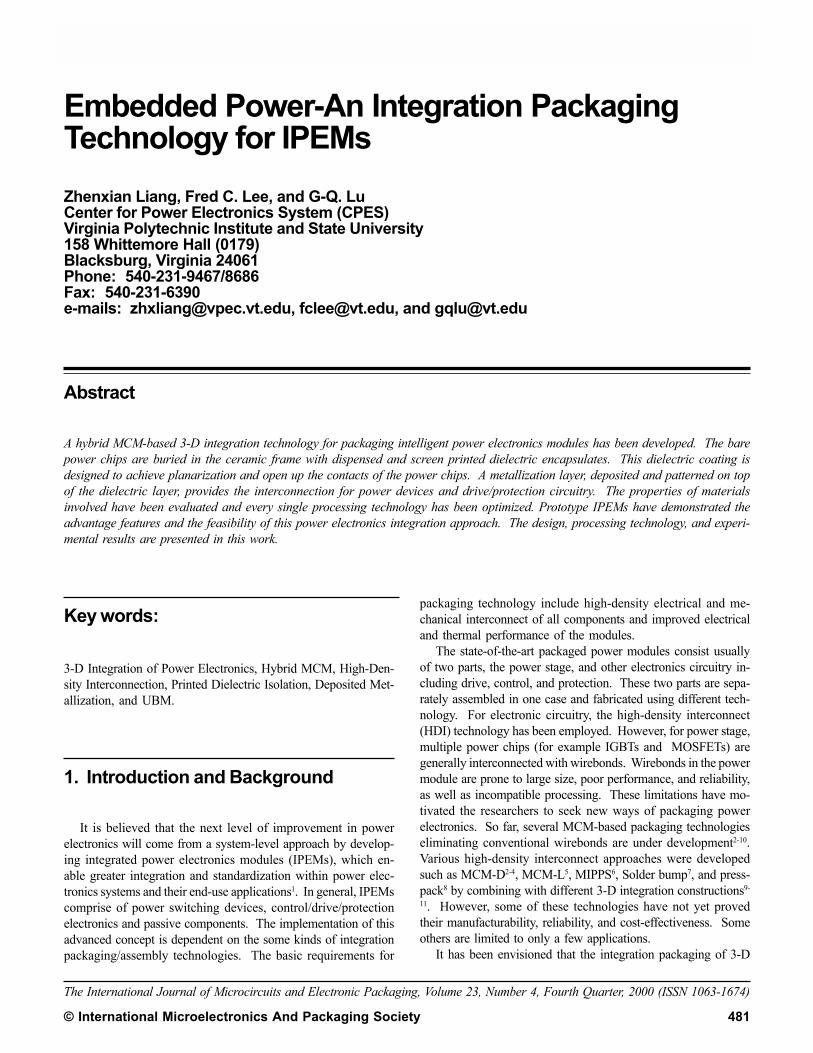
Figure 1 illustrates the conceptual structure of embedded powermodule. It consists of three parts-embedded power stage, basesubstrate, and electronic circuitry, which are soldered together tobuild an IPEM module. The electronic components representdriver, control, and protection circuitry. The base substrate pro-vides electrical interconnection and high thermal-conductivitypath of power chips. The core element in this structure is thepower stage that comprises of ceramic frame, power chips (SI inthe Figure) and isolation dielectric, as well as metallization cir-
cuit. This element provides the high-density 3-D interconnec-tion of IPEM components.
����������������������������������������������������
������������������
����������������������
��������������������������������������������������������
����������������������������������������������������������������������
��������������������������������������������������������������������
SI SI
����������������������
����������������������
Solder
Metallization
����������������������������������������������������
������������������������������������������������������������������������������������������������������
Substrate
Components
Ceramic
Dielectric
Figure 1. Schematic integration structure of embeddedpower IPEM.
The main feature of this integration design, differing fromother 3-dimensional packaging approaches, is that the multiplenon-solderable power semiconductor chips are directly integratedeach other and with other electronic circuitry. The special isola-tion/interconnect construction with embedded chips offers muchhigher integration. Due to the larger contact area, sandwich powerbus layout and short signal distance, much lower parasitic is an-ticipated along with improved heat dissipation through the largearea metallization. In view of process technology, low-tempera-ture hybrid processing techniques can be employed to fabricateall structural layers. In addition, it has the capability of incorpo-rating other power electronic components such as hybrid inter-connection on ceramic substrate and integrated capacitors/ in-ductors in planar form.
However, since a few kinds of materials are tightly stackedtogether, the module contains many interfaces with potential re-sidual stress. The modules are designed to process large currentat high voltage level, as well as working at high temperature.Therefore, there are some challenge such as structure integrity,thermal match, power capability, and feasibility of the technol-ogy. To solve these problems, material selection, process tech-nology development, and implementation are basic issues.
3. Design and TechnologyDevelopment
The implementation of the proposed Embedded Power con-cept needs understand of electrical and thermal characteristicsfor multilayer structure. The novel simulation tools have beenused for analysis and optimization. Materials used in the struc-ture must offer good comprehensive performance including me-chanical, electrical, and thermal, as well as processing proper-

Embedded Power-An Integration Packaging Technology for IPEMs
The International Journal of Microcircuits and Electronic Packaging, Volume 23, Number 4, Fourth Quarter, 2000 (ISSN 1063-1674)
© International Microelectronics And Packaging Society 483
ties. Experimental investigation method is very important totailor and apply these advanced materials.
The main issues addressed include high current and high volt-age capabilities of interconnect system, high thermal dissipation,and structure integrity. Electrical simulation for high perfor-mance and thermal-mechanical analysis for high reliability havebeen performed. The final material combination and contactscheme in the structure are as follows. The power chips areembedded in a ceramic carrier by filling the gap. A selecteddielectric layer is coated on the chip surface with openings up thecontact pads of the power chips. This interlayer provides encap-sulate for electrical isolation of power devices and other circuitry.A deposited metal (Cu) circuit (pattern) is designed to connectthe Al pads (after dielectric coating with via hole on pad) of thepower chips to external driver/control and protection circuitry.To accomplish this metallurgical interconnect, the under bumpmetallization (UBM) schemes used widely in IC packaging areemployed in this approach. The UBM schemes such as Ti-Ni-Cu or Cr-Ni-Cu layers provide low film stress with the goodadhesive and electrical/thermal conduction. For high currentrequirement, an Electro-plated Cu layer is added to the thin sput-tered Cu layer of the UBM scheme. Figure 2 illustrates sche-matically the details of the contact scheme.
Plated CuSputtered CuSputtered NiSputtered Cr/TiAl Pad on Chip
����������������������������������������������������������������
������������������������������������������������������������������SI
��������������������������������������������� ����� ������������ ������������
����������������������������������������������������������������
��������������������������������
���������������������������������
IGBT orMOSFETChip
Drain Contact(Solderable)
Dielectric andPassivation
Figure 2. The contact scheme in embedded power stage.
The key to accomplish Embedded Power concept is to applyselected materials into designed structure. The packaging tech-nologies for power electronics have not kept pace with those oflow power electronics, like the packaging of microelectronics.But existing thin film and thick film processing techniques canbe employed and modified to apply in power packaging. Theseefforts can also results in cost-effectiveness technology for largeamount of production. Table 1 lists the fabrication steps of Em-bedded power stage including issues and specific processing so-lutions. The researchers have experimentally investigated andcompared different alternatives for each processing. Finally, anall-low temperature (<250°C) hybrid technology to fabricate theembedded power stage has been used, which is a set of mask-based processing. The base substrate and the metallizationcircuit are patterned by photolithography technique. Dielectricpolymer is applied with pattern-screen printing method and chip-carrier is fabricated by computer controlled laser cutting.
Table 1. Processing scheme of embedded power.
4. Fabrication of Prototype Module
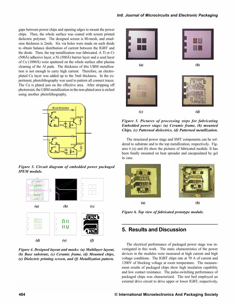
Figure 3 shows the circuit diagram of the prototype IPEMmodule consisting of two IGBTs, two power diodes and gate driv-ers (one leg inverter). Two IGBTs and two diodes are bare chips(size: 7.9×9.1mm2). There are six-emitter Al pads (1.1×1.1 mm2)and one-gate Al pad (1.1×1.1mm2) on the upper side of eachIGBT. A larger Al pad on the upper side of the diode is 7×8.5mm2.The backsides of all device chips are gold metallization as drainor cathode, which is solderable and can directly soldered to sub-strate. All drive/control components are surface-mountable. Fig-ures 4 (a)-(f) present the designed layouts and masks used indifferent processing. A 2”×2”AlN DBC substrate with 10mil-thick-Cu on both sides of 25mil-thick-ceramic is used as basesubstrate, which will be etched on one side (b) and another sideis ready for soldering to heat spreader. A 2”×2”Al2O3 ceramicplate with a thickness of 25 mils will be machined to have fouropenings for mount of two IGBTs and two diode chips. Threeedge windows for output of three power terminals. This ceramicframe will be used as chip carrier (c). The dielectric layer isdesigned to open via holes on the pads of power chips (e). Met-allization layer is patterned to connect all pads and mountablecomponents (f). Figure 5 shows the pictures of the processedpower stage element. The dielectric paste was dispensed in the
© International Microelectronics And Packaging Society
The International Journal of Microcircuits and Electronic Packaging, Volume 23, Number 4, Fourth Quarter, 2000 (ISSN 1063-1674)
Intl. Journal of Microcircuits and Electronic Packaging
484
gaps between power chips and opening edges to mount the powerchips. Then, the whole surface was coated with screen printeddielectric polymer. The designed screen is 80-mesh, and emul-sion thickness is 2mils. Six via holes were made on each diodeto obtain balance distribution of current between the IGBT andthe diode. Then, the top metallization was fabricated. A Ti or Cr(500Å) adhesive layer, a Ni (500Å) barrier layer and a seed layerof Cu (1000Å) were sputtered on the whole surface after plasmacleaning of the Al pads. The thickness of this UBM metalliza-tion is not enough to carry high current. Therefore, an electro-plated Cu layer was added up to the 5mil thickness. In the ex-periment, photolithography was used to pattern all connect traces.The Cu is plated just on the effective area. After stripping offphotoresist, the UBM metallization in the non-plated area is etchedusing another photolithography.
IGBT IGBT DIODE DIODE
IGBT IGBT DIODE DIODE
15V 15V
-5V -5V
15V 15V
-5V -5V
R R g1
R R g2 g2
R R g1
R R g2
R R 1 1 TVS TVS
TVS TVS R R 1 1
De-sat Protection De-sat Protection
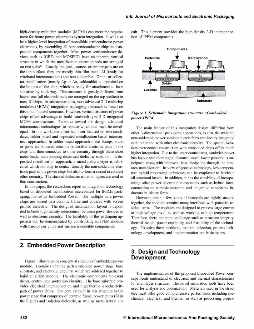
Figure 3. Circuit diagram of embedded power packagedIPEM module.
(a) (b) (c)
(d) (e) (f)
Figure 4. Designed layout and masks: (a) Multilayer layout,(b) Base substrate, (c) Ceramic frame, (d) Mounted chips,(e) Dielectric printing screen, and (f) Metallization pattern.
(a) (b)
(c) (d)
Figure 5. Pictures of processing steps for fabricatingEmbedded power stage: (a) Ceramic frame, (b) mountedChips, (c) Patterned dielectrics, (d) Patterned metallization.
The structured power stage and SMT components can be sol-dered to substrate and to the top metallization, respectively. Fig-ures 6 (a) and (b) show the pictures of fabricated module. It hasbeen finally mounted on heat spreader and encapsulated by gelin case.
(a) (b)
Figure 6. Top view of fabricated prototype module.
5. Results and Discussion
The electrical performance of packaged power stage was in-vestigated in this work. The static characteristics of the powerdevices in the modules were measured at high current and highvoltage conditions. The IGBT chips rate at 70 A of current and1200V of blocking voltage at room temperature. The measure-ment results of packaged chips show high insulation capabilityand low contact resistance. The pulse-switching performance ofpackaged chips was characterized. The test bed employed anexternal drive circuit to drive upper or lower IGBT, respectively,
Embedded Power-An Integration Packaging Technology for IPEMs
The International Journal of Microcircuits and Electronic Packaging, Volume 23, Number 4, Fourth Quarter, 2000 (ISSN 1063-1674)
© International Microelectronics And Packaging Society 485
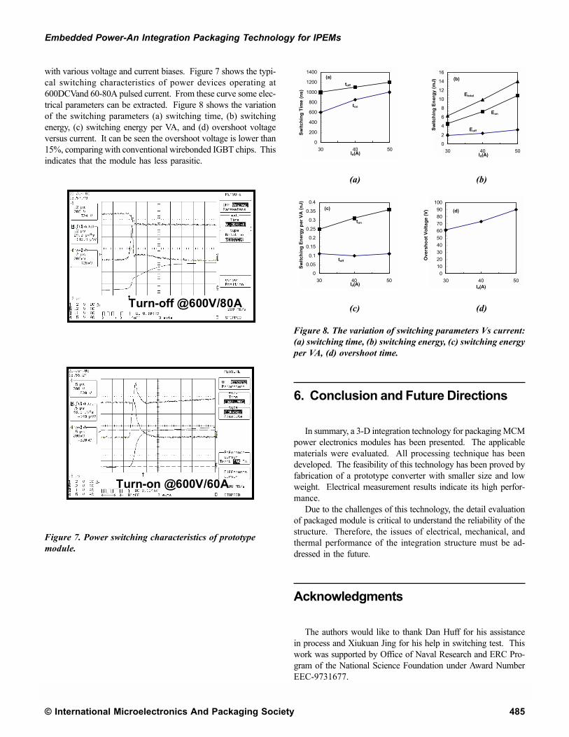
with various voltage and current biases. Figure 7 shows the typi-cal switching characteristics of power devices operating at600DCVand 60-80A pulsed current. From these curve some elec-trical parameters can be extracted. Figure 8 shows the variationof the switching parameters (a) switching time, (b) switchingenergy, (c) switching energy per VA, and (d) overshoot voltageversus current. It can be seen the overshoot voltage is lower than15%, comparing with conventional wirebonded IGBT chips. Thisindicates that the module has less parasitic.
Turn-off @600V/80A
Turn-on @600V/60A
Figure 7. Power switching characteristics of prototypemodule.
0
2
4
6
8
10
12
14
16
30 40 50
Eoff
Eon
Switc
hing
Ene
rgy
(mJ)
Etotal
Id(A)
(b)
0
200
400
600
800
1000
1200
1400
30 40 50
toff
ton
Id(A)
Switc
hing
Tim
e (n
s)
(a)
(a) (b)
0102030405060708090100
30 40 50Id(A)
Ove
rsho
ot V
olta
ge (V
) (d)
0
0.05
0.1
0.15
0.2
0.25
0.3
0.35
0.4
30 40 50
toff
ton
Id(A)
Switc
hing
Ene
rgy
per V
A (n
J)
(c)
(c) (d)
Figure 8. The variation of switching parameters Vs current:(a) switching time, (b) switching energy, (c) switching energyper VA, (d) overshoot time.
6. Conclusion and Future Directions
In summary, a 3-D integration technology for packaging MCMpower electronics modules has been presented. The applicablematerials were evaluated. All processing technique has beendeveloped. The feasibility of this technology has been proved byfabrication of a prototype converter with smaller size and lowweight. Electrical measurement results indicate its high perfor-mance.
Due to the challenges of this technology, the detail evaluationof packaged module is critical to understand the reliability of thestructure. Therefore, the issues of electrical, mechanical, andthermal performance of the integration structure must be ad-dressed in the future.
Acknowledgments
The authors would like to thank Dan Huff for his assistancein process and Xiukuan Jing for his help in switching test. Thiswork was supported by Office of Naval Research and ERC Pro-gram of the National Science Foundation under Award NumberEEC-9731677.
© International Microelectronics And Packaging Society
The International Journal of Microcircuits and Electronic Packaging, Volume 23, Number 4, Fourth Quarter, 2000 (ISSN 1063-1674)
Intl. Journal of Microcircuits and Electronic Packaging
486
References
1. J. D. Van Wyk and F. C. Lee, “Power Electronics Technology(status and Future)”, Proceedings of 17th Annual Power Elec-tronics Seminar at Virginia Tech, VPEC Seminar ‘99,Blacksburg, Virginia, pp. 61-70, September 19-21, 1999.
2. Errol Porter, S. Ang, K. Burgers, M. Glover, and K.Olegjniczak, “Power Electronics Combines with MCM Tech-nology to Create Multichip Power Modules”, Proceedings of30th International Symposium on Microelectronics, IMAPS‘97, Philadelphia, Pennsylvania, pp. 78-83, 1997.
3. R. Fisher, R. Fillion, J. Burgess, and W. Hennessy, “HighFrequency, Low Cost, Power Packaging Using Thin FilmPower Overlay Technology”, Proceedings of 10th AnnualApplied Power Electronics Conference and Exposition,APEC’95, Dallas, Texas, March 5-9, pp. 12-17, 1995.
4. A. Collado, X. Jorda, E.Cabruja, and P. Godignon, “MCM-DPackaging for Power Applications”, Proceedings of Interna-tional workshop on Integrated Power Packaging, July 14-16,Waltham, Massachusetts, pp. 69-73, 2000.
5. R. W. Linden, L. Duncan, and R. Fryhoff, “Low-cost Inte-grated Power Module Technology”, Proceedings of the 37thInternational Power Electronics Conference, PCIM ’98, SantaClara, California, pp. 130-140, 1998.
6. S. Haque, K. Xing, R-L. Lin, C. Suchicital, G-Q. Lu, D. J.Nelson, D. Borojevic, and F. C. Lee, “An Innovative Tech-nique for Packaging Power Electronics Building Blocks Us-ing Metal Posts Interconnected Parallel Plate Structures,”Transactions of Components, Packaging, and ManufacturingTechnology, Part B, Vol. 22, No. 2, pp. 136-144, May 1999.
7. X. Liu, S. Haque, J. Wang, and G-Q, Lu, “Packaging of Inte-grated Power Electronics Modules Using Flip Chip Technol-ogy”, Proceedings of 15th Annual Applied Power Electronicsand Exposition, APEC ‘00, New Orleans, Louisiana, pp. 290-296, February 2000.
8. A. Pirond, G. Nicoletto, P. Cova, M. Pasqualetti, M. Portesine,and P. E. Zani, “Thermo-Mechanical Simulation of a MultichipPress-Packed IGBT”, Solid State Electronics, Vol. 42, No.12, pp. 2303-2307, December 1998.
9. A. B. Lostetter, F. Barlow, and A. Elshabini, “ MultilayerInterconnects for a High Power Packaging Strategy,” Proceed-ings of IMAPS 1998 International Symposium on Microelec-tronics, IMAP ‘98, San Diego, California, pp. 330-334, 1998.
10. J. A. Ferreira, I. W. Hofsajer, and J. D. Van Wyk, “Exploit-ing the Third Dimension in Power Electronics Packaging”,Proceedings of the 12th Annual Applied Power Electronicsand Exposition, APEC’97, Atlanta, Georgia, February 23-27,pp. 419-423, 1997.
11. Z. X. Liang, G-Q. Lu, D. Borojevic, and F. C. Lee, “Mul-tilayer Integration Technology for Packaging of IPEM”, Pro-ceedings of 17th CPES Seminar, Blacksburg, Virginia, pp.181-183, September 1999.
12. Z. X. Liang, F. C. Lee, G-Q. Lu, and D. Borojevic, “Embed-ded Power –a Multilayer Integration Technology for Packag-
ing of IPEMs and PEBBs,” Proceedings of International Work-shop on Integrated Power Packaging, Waltham, Massachu-setts, pp. 41-45, July 14-16, 2000.
About the authors
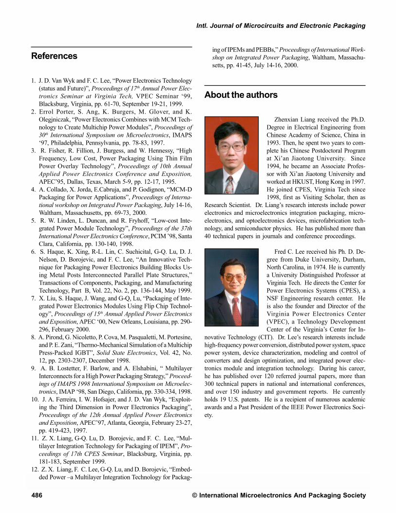
Zhenxian Liang received the Ph.D.Degree in Electrical Engineering fromChinese Academy of Science, China in1993. Then, he spent two years to com-plete his Chinese Postdoctoral Programat Xi’an Jiaotong University. Since1994, he became an Associate Profes-sor with Xi’an Jiaotong University andworked at HKUST, Hong Kong in 1997.He joined CPES, Virginia Tech since1998, first as Visiting Scholar, then as
Research Scientist. Dr. Liang’s research interests include powerelectronics and microelectronics integration packaging, micro-electronics, and optoelectronics devices, microfabrication tech-nology, and semiconductor physics. He has published more than40 technical papers in journals and conference proceedings.
Fred C. Lee received his Ph. D. De-gree from Duke University, Durham,North Carolina, in 1974. He is currentlya University Distinguished Professor atVirginia Tech. He directs the Center forPower Electronics Systems (CPES), aNSF Engineering research center. Heis also the founder and Director of theVirginia Power Electronics Center(VPEC), a Technology DevelopmentCenter of the Virginia’s Center for In-
novative Technology (CIT). Dr. Lee’s research interests includehigh-frequency power conversion, distributed power system, spacepower system, device characterization, modeling and control ofconverters and design optimization, and integrated power elec-tronics module and integration technology. During his career,he has published over 120 referred journal papers, more than300 technical papers in national and international conferences,and over 150 industry and government reports. He currentlyholds 19 U.S. patents. He is a recipient of numerous academicawards and a Past President of the IEEE Power Electronics Soci-ety.

Embedded Power-An Integration Packaging Technology for IPEMs
The International Journal of Microcircuits and Electronic Packaging, Volume 23, Number 4, Fourth Quarter, 2000 (ISSN 1063-1674)
© International Microelectronics And Packaging Society 487
Guo-Quan Lu received his Ph.D.Degree in Applied Physics/MaterialsScience from Harvard University in1990. From 1990 to 1992, Dr. Luworked for Alcoa Electronic Packaging,Inc., at Alcoa Technical Center, Pitts-burgh, Pennsylvania. In 1992, Dr. Lujoined the faculty of the Department ofMaterials Science and Engineering atVirginia Tech. Currently, he is an As-sociate Professor jointly appointed be-
tween the Department of Materials Science and Engineering andthe Bradley Department of Electrical and Computer Engineer-ing. His research interests include processing of electronic andoptoelectronic materials and devices, and integration, packag-ing, and reliability of microelectronic, power electronic, and op-toelectronic modules/systems. Dr. Lu holds two U.S. patents andhas published over 70 papers in journals and conference pro-ceedings.