surface mount manufacturing basics
TRANSCRIPT
May 3, 2023
Surface Mount Manufacturing Basics
Familiarization information for SMT printed circuit board production
May 3, 2023page 2 /
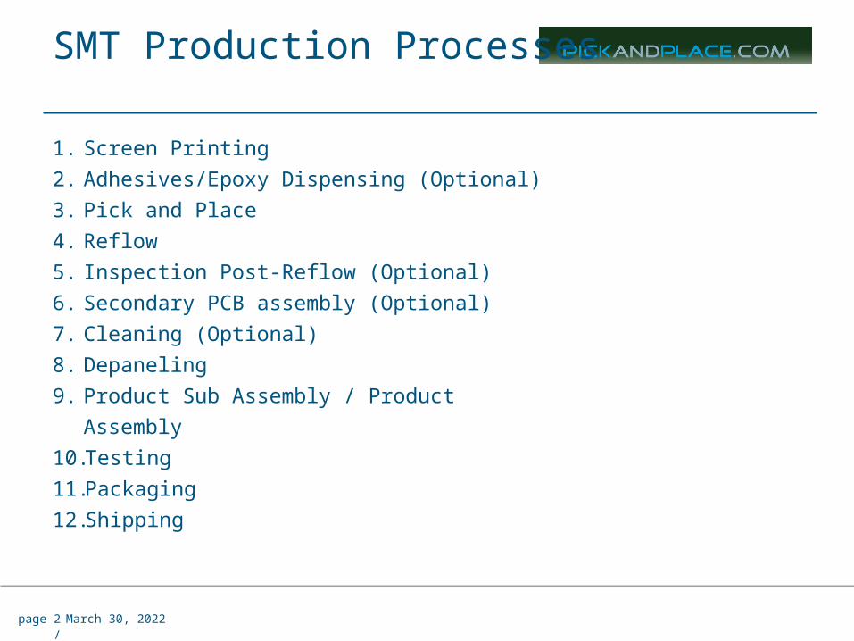
SMT Production Processes
1. Screen Printing2. Adhesives/Epoxy Dispensing (Optional)3. Pick and Place4. Reflow5. Inspection Post-Reflow (Optional)6. Secondary PCB assembly (Optional)7. Cleaning (Optional)8. Depaneling9. Product Sub Assembly / Product Assembly10.Testing11.Packaging12.Shipping
May 3, 2023page 3 /
Processes Defined
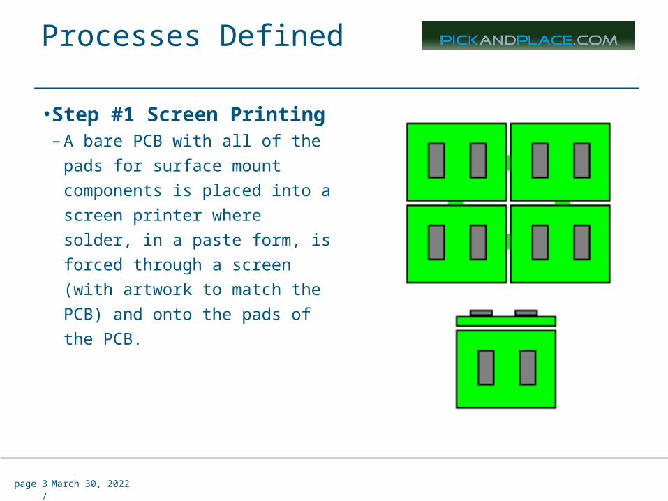
• Step #1 Screen Printing– A bare PCB with all of the pads
for surface mount components is placed into a screen printer where solder, in a paste form, is forced through a screen (with artwork to match the PCB) and onto the pads of the PCB.
May 3, 2023page 4 /
Processes Defined
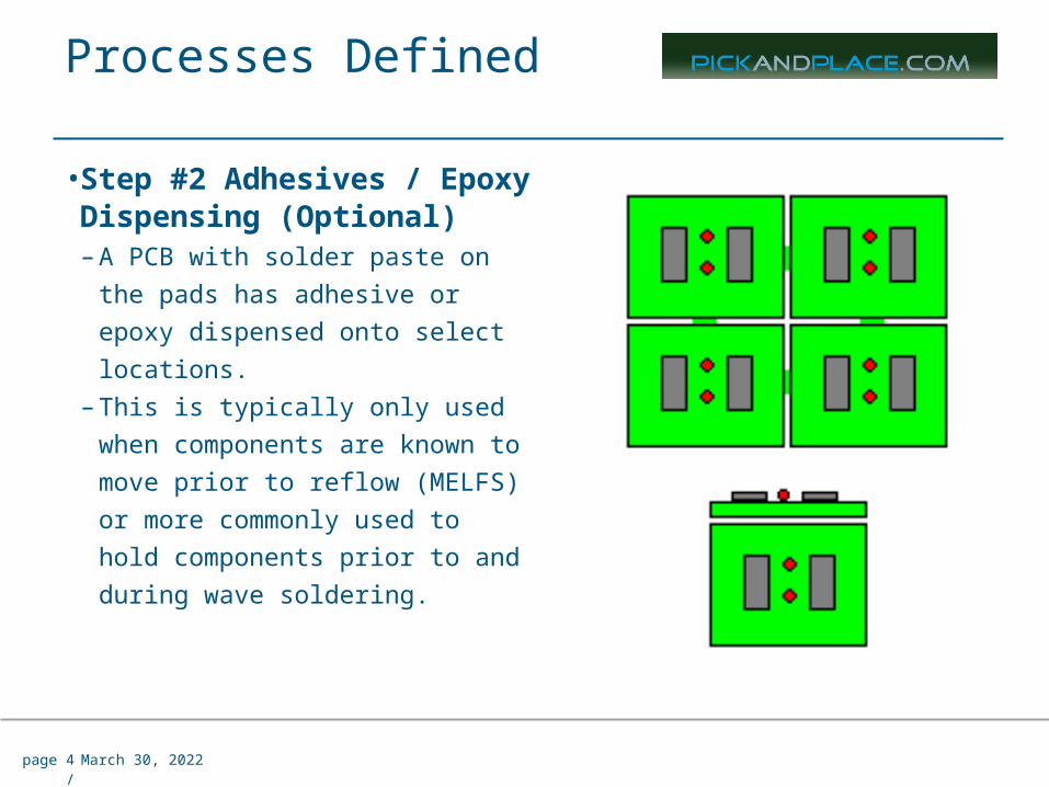
• Step #2 Adhesives / Epoxy Dispensing (Optional)– A PCB with solder paste on the
pads has adhesive or epoxy dispensed onto select locations.
– This is typically only used when components are known to move prior to reflow (MELFS) or more commonly used to hold components prior to and during wave soldering.
May 3, 2023page 5 /
Processes Defined
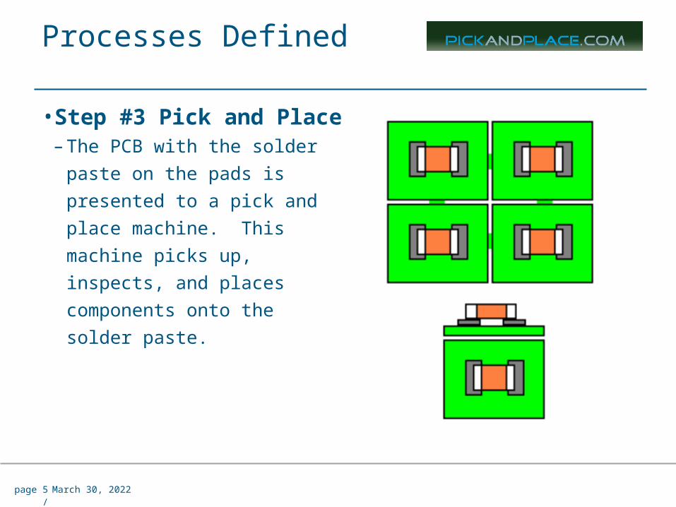
• Step #3 Pick and Place– The PCB with the solder paste
on the pads is presented to a pick and place machine. This machine picks up, inspects, and places components onto the solder paste.
May 3, 2023page 6 /
Processes Defined
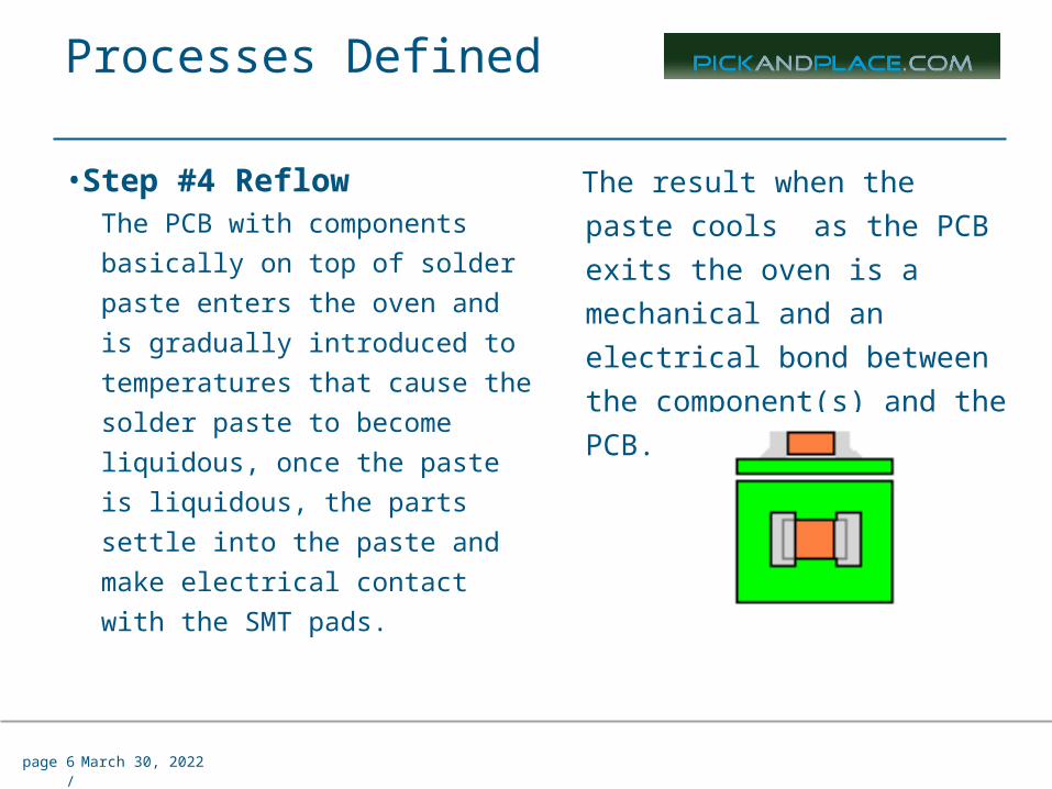
• Step #4 ReflowThe PCB with components basically on top of solder paste enters the oven and is gradually introduced to temperatures that cause the solder paste to become liquidous, once the paste is liquidous, the parts settle into the paste and make electrical contact with the SMT pads.
The result when the paste cools as the PCB exits the oven is a mechanical and an electrical bond between the component(s) and the PCB.
May 3, 2023page 7 /
Processes Defined
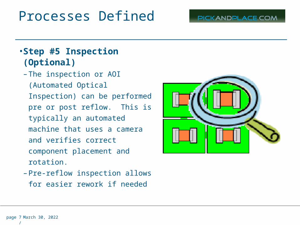
• Step #5 Inspection (Optional)– The inspection or AOI
(Automated Optical Inspection) can be performed pre or post reflow. This is typically an automated machine that uses a camera and verifies correct component placement and rotation.
– Pre-reflow inspection allows for easier rework if needed
May 3, 2023page 8 /
Processes Defined
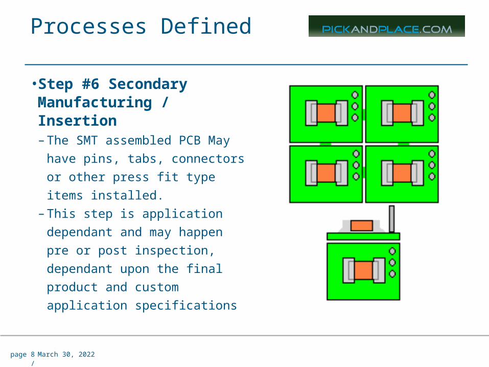
• Step #6 Secondary Manufacturing / Insertion– The SMT assembled PCB May
have pins, tabs, connectors or other press fit type items installed.
– This step is application dependant and may happen pre or post inspection, dependant upon the final product and custom application specifications
May 3, 2023page 9 /
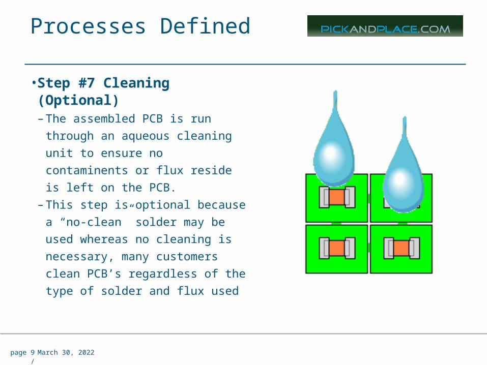
Processes Defined
• Step #7 Cleaning (Optional)– The assembled PCB is run
through an aqueous cleaning unit to ensure no contaminents or flux reside is left on the PCB.
– This step is optional because a “no-clean” solder may be used whereas no cleaning is necessary, many customers clean PCB’s regardless of the type of solder and flux used
May 3, 2023page 10 /
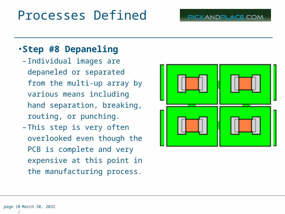
Processes Defined
• Step #8 Depaneling – Individual images are depaneled
or separated from the multi-up array by various means including hand separation, breaking, routing, or punching.
– This step is very often overlooked even though the PCB is complete and very expensive at this point in the manufacturing process.
May 3, 2023page 11 /
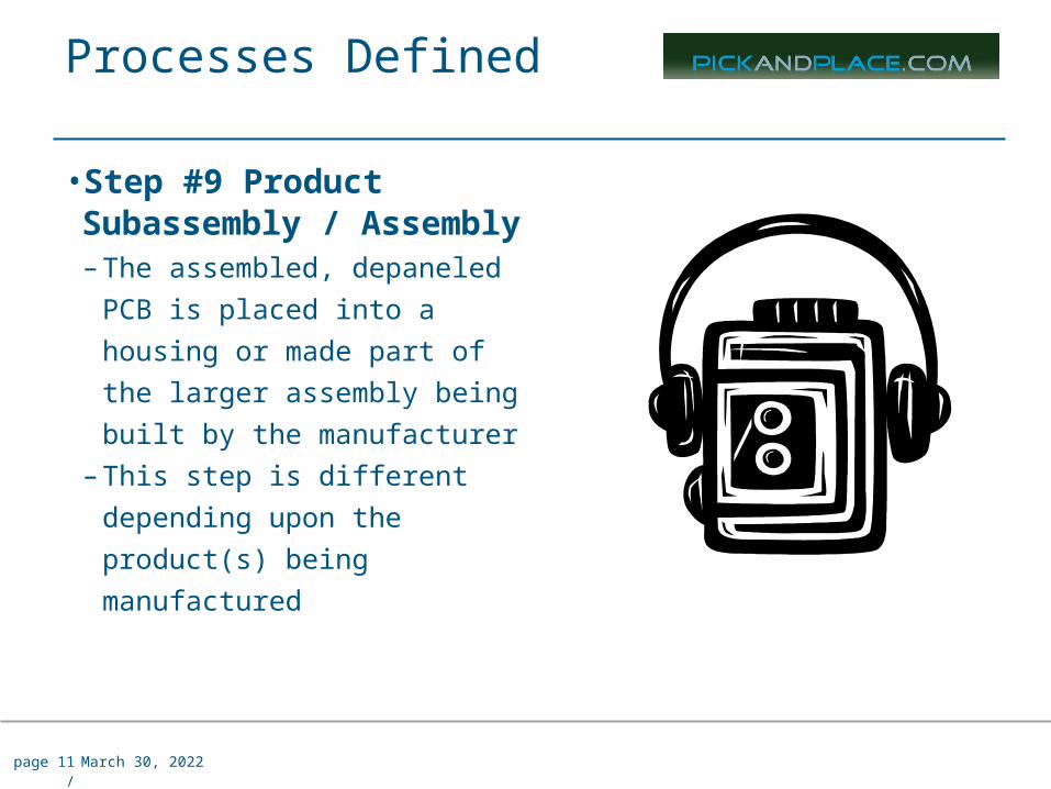
Processes Defined
• Step #9 Product Subassembly / Assembly – The assembled, depaneled
PCB is placed into a housing or made part of the larger assembly being built by the manufacturer
– This step is different depending upon the product(s) being manufactured
May 3, 2023page 12 /
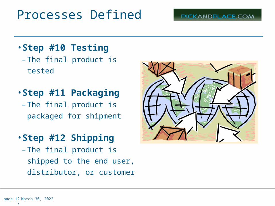
Processes Defined
• Step #10 Testing– The final product is tested
• Step #11 Packaging– The final product is packaged for
shipment
• Step #12 Shipping– The final product is shipped to
the end user, distributor, or customer