fabrication and manufacturing (basics) -...
TRANSCRIPT
EE 261 James Morizio 1
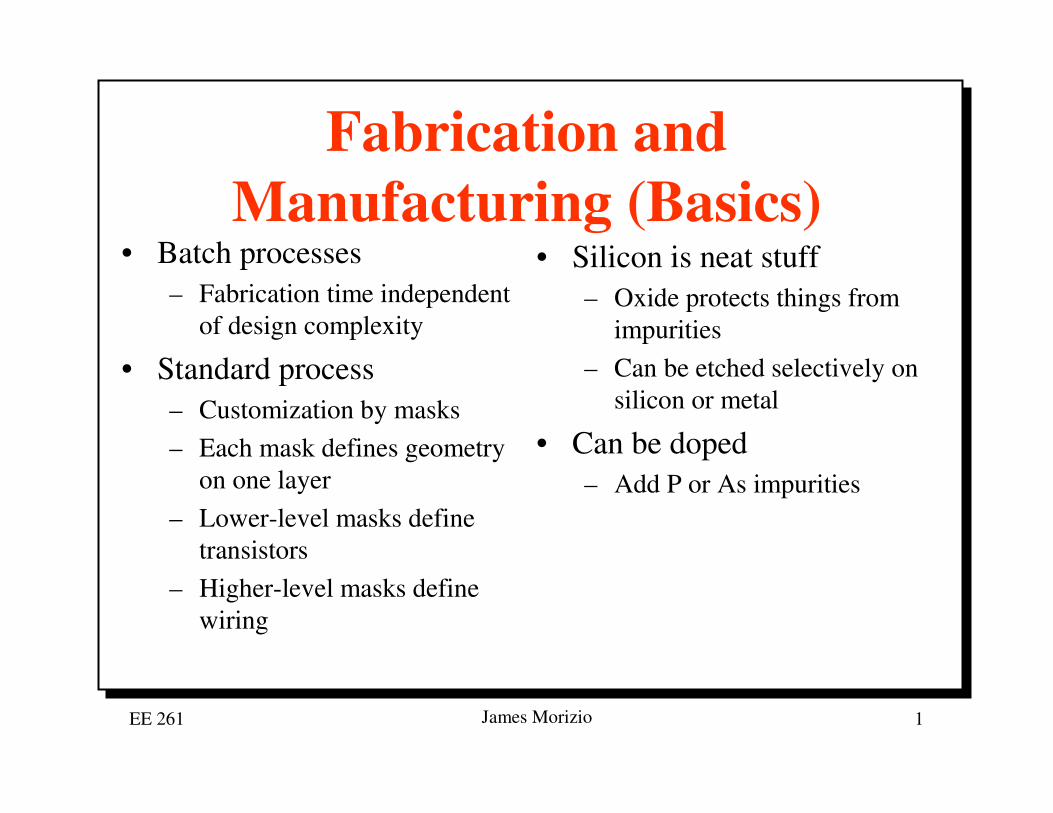
Fabrication and Manufacturing (Basics)
• Batch processes– Fabrication time independent
of design complexity
• Standard process– Customization by masks– Each mask defines geometry
on one layer– Lower-level masks define
transistors– Higher-level masks define
wiring
• Silicon is neat stuff– Oxide protects things from
impurities– Can be etched selectively on
silicon or metal
• Can be doped– Add P or As impurities

EE 261 James Morizio 2
CMOS Fabrication
• CMOS transistors are fabricated on silicon wafer• Lithography process similar to printing press• On each step, different materials are deposited or
etched• Easiest to understand by viewing both top and
cross-section of wafer in a simplified manufacturing process
EE 261 James Morizio 3
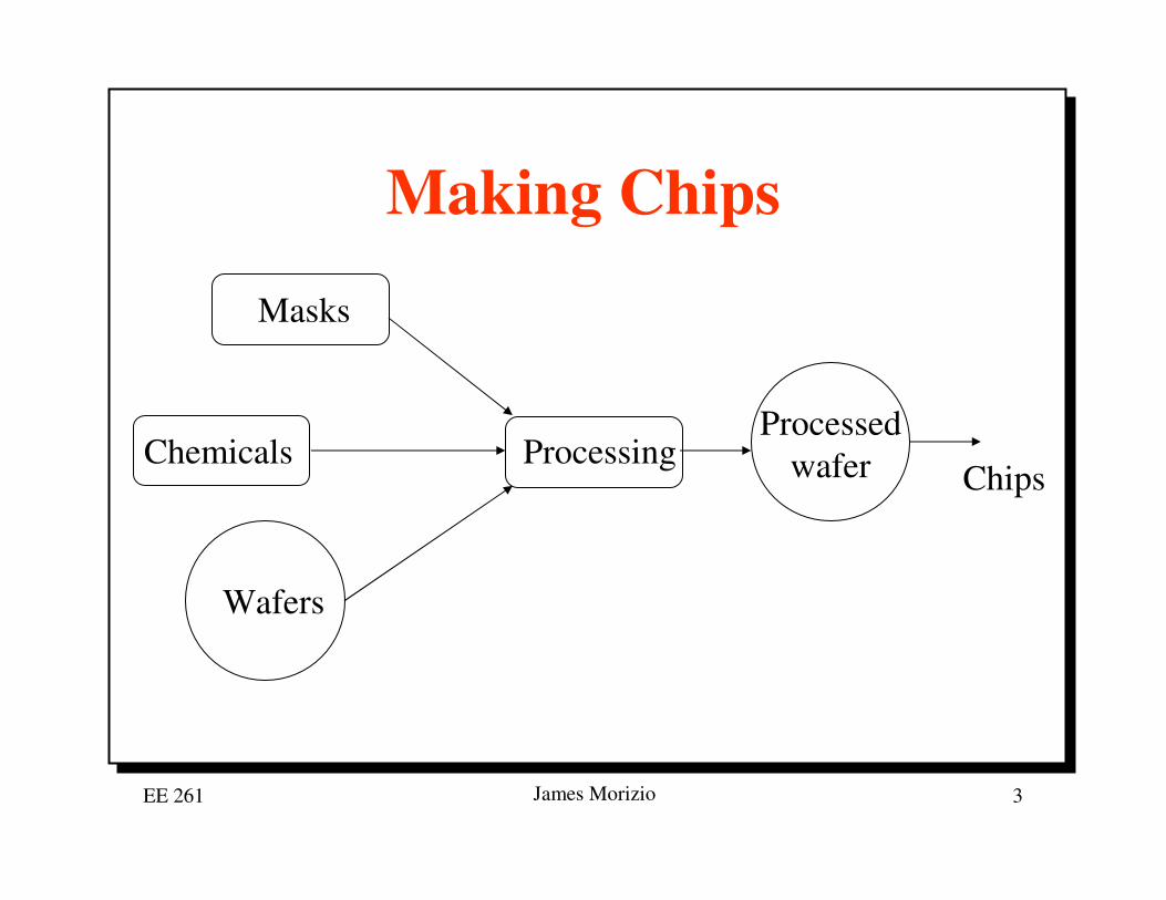
Making Chips
Chemicals
Wafers
Masks
ProcessingProcessed
wafer Chips
EE 261 James Morizio 4
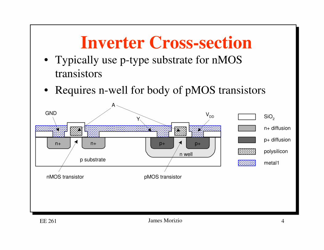
Inverter Cross-section• Typically use p-type substrate for nMOS
transistors• Requires n-well for body of pMOS transistors
n+
p substrate
p+
n well
A
YGND VDD
n+ p+
SiO2
n+ diffusion
p+ diffusion
polysilicon
metal1
nMOS transistor pMOS transistor
EE 261 James Morizio 5
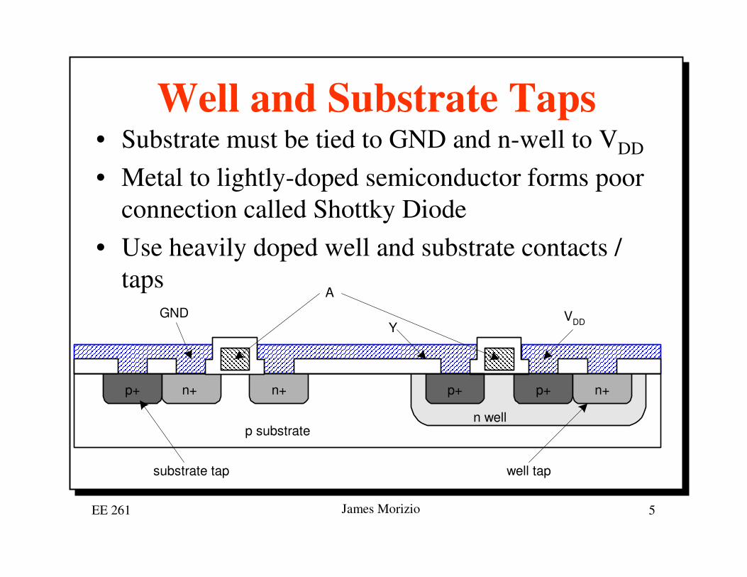
Well and Substrate Taps• Substrate must be tied to GND and n-well to VDD
• Metal to lightly-doped semiconductor forms poor connection called Shottky Diode
• Use heavily doped well and substrate contacts / taps
n+
p substrate
p+
n well
A
YGND VDD
n+p+
substrate tap well tap
n+ p+
EE 261 James Morizio 6
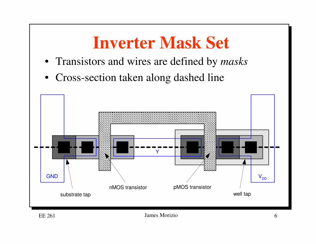
Inverter Mask Set• Transistors and wires are defined by masks• Cross-section taken along dashed line
GND VDD
Y
A
substrate tap well tapnMOS transistor pMOS transistor

EE 261 James Morizio 7
Detailed Mask Views
• Six masks– n-well– Polysilicon– n+ diffusion– p+ diffusion– Contact– Metal
Metal
Polysilicon
Contact
n+ Diffusion
p+ Diffusion
n well
EE 261 James Morizio 8
Basic Processing Steps
• N-diffusion created by doping regions of the substrate
• Poly and metal are laid over the substrate, with oxide to insulate them from substrate and each other
• Wires are added in layers, alternating with oxide• Vias are cut in the oxide
EE 261 James Morizio 9
Fabrication Steps
• Features are patterned on a wafer by a photolithographic process– Photo-light lithography, n. process of printing from a plane surface
on which image to be printed is ink-receptive and the blank area is ink-repellant
• Cover the wafer with a light-sensitive, organic material called photoresist
• Expose to light with the proper pattern (mask)• Patterns left by photoresist can be used to control where
oxide is grown or materials are placed on surface of wafer
EE 261 James Morizio 10
Fabrication Steps• Layout contains information on what patterns have
to made on the wafer• Masks are created using the layout information
provided by the designer• Procedure involves selective removal of the oxide
– Coat the oxide with photoresist, polymerized by UV light (applied through mask)
– Polymerized photoresist dissolves in acid– Photoresist itself is acid-resistant
EE 261 James Morizio 11
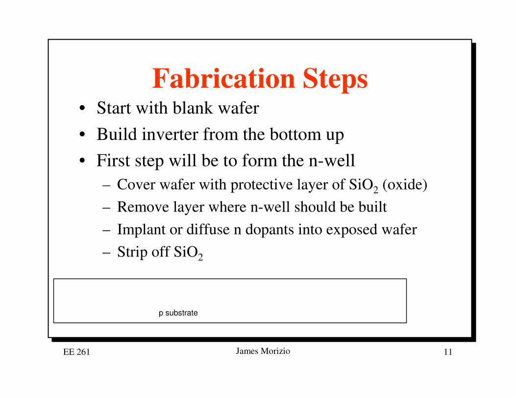
Fabrication Steps• Start with blank wafer• Build inverter from the bottom up• First step will be to form the n-well
– Cover wafer with protective layer of SiO2 (oxide)– Remove layer where n-well should be built– Implant or diffuse n dopants into exposed wafer– Strip off SiO2
p substrate

EE 261 James Morizio 12
Oxidation
• Grow SiO2 on top of Si wafer– 900 – 1200 C with H2O or O2 in oxidation furnace
p substrate
SiO2
EE 261 James Morizio 13
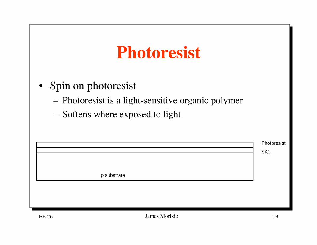
Photoresist
• Spin on photoresist– Photoresist is a light-sensitive organic polymer– Softens where exposed to light
p substrate
SiO2
Photoresist
EE 261 James Morizio 14
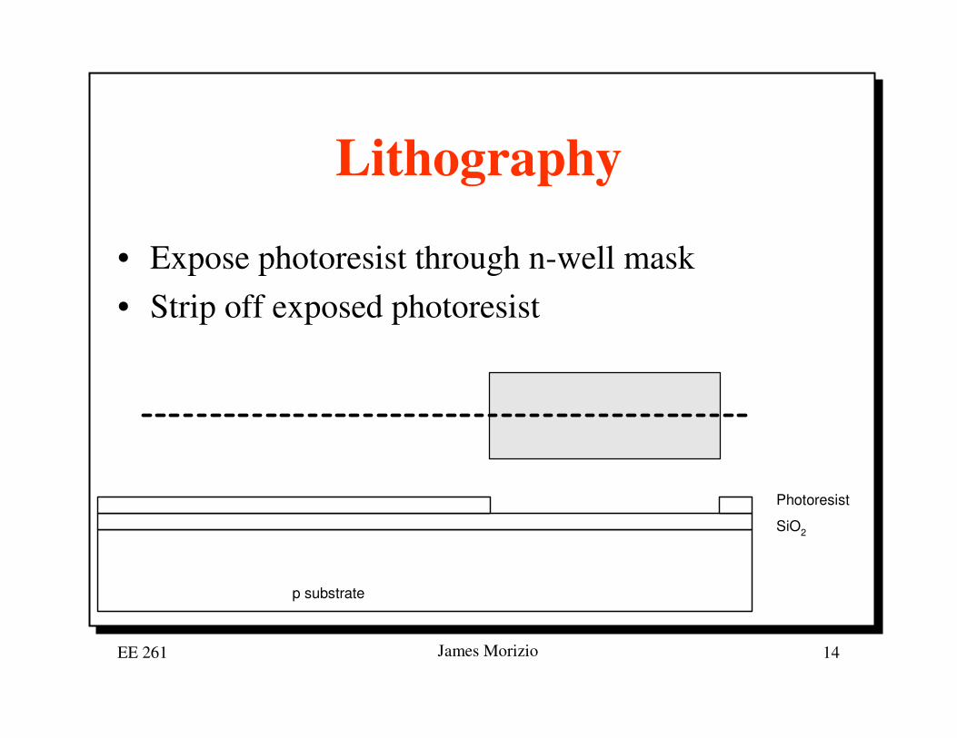
Lithography
• Expose photoresist through n-well mask• Strip off exposed photoresist
p substrate
SiO2
Photoresist

EE 261 James Morizio 15
Etch
• Etch oxide with hydrofluoric acid (HF)– Seeps through skin and eats bone; nasty stuff!!!
• Only attacks oxide where resist has been exposed
p substrate
SiO2
Photoresist

EE 261 James Morizio 16
Strip Photoresist
• Strip off remaining photoresist– Use mixture of acids called piranah etch
• Necessary so resist doesn’t melt in next step
p substrate
SiO2
EE 261 James Morizio 17
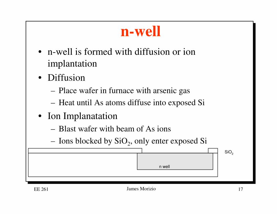
n-well• n-well is formed with diffusion or ion
implantation• Diffusion
– Place wafer in furnace with arsenic gas– Heat until As atoms diffuse into exposed Si
• Ion Implanatation– Blast wafer with beam of As ions– Ions blocked by SiO2, only enter exposed Si
n well
SiO2

EE 261 James Morizio 18
Strip Oxide
• Strip off the remaining oxide using HF• Back to bare wafer with n-well• Subsequent steps involve similar series of steps
p substraten well

EE 261 James Morizio 19
Polysilicon
• Deposit very thin layer of gate oxide– < 20 Å (6-7 atomic layers)
• Chemical Vapor Deposition (CVD) of silicon layer– Place wafer in furnace with Silane gas (SiH4)– Forms many small crystals called polysilicon– Heavily doped to be good conductor
Thin gate oxidePolysilicon
p substraten well
EE 261 James Morizio 20
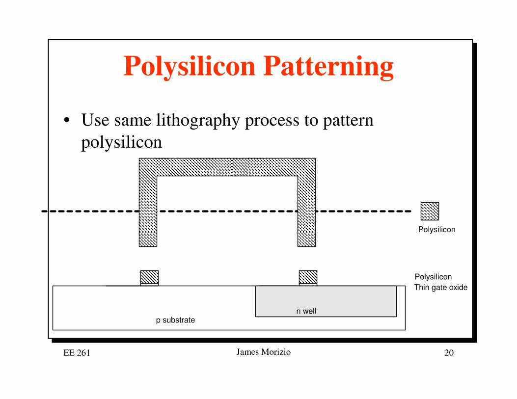
Polysilicon Patterning
• Use same lithography process to pattern polysilicon
Polysilicon
p substrate
Thin gate oxidePolysilicon
n well

EE 261 James Morizio 21
Self-Aligned Process
• Use oxide and masking to expose where n+ dopants should be diffused or implanted
• N-diffusion forms nMOS source, drain, and n-well contact
p substraten well
EE 261 James Morizio 22
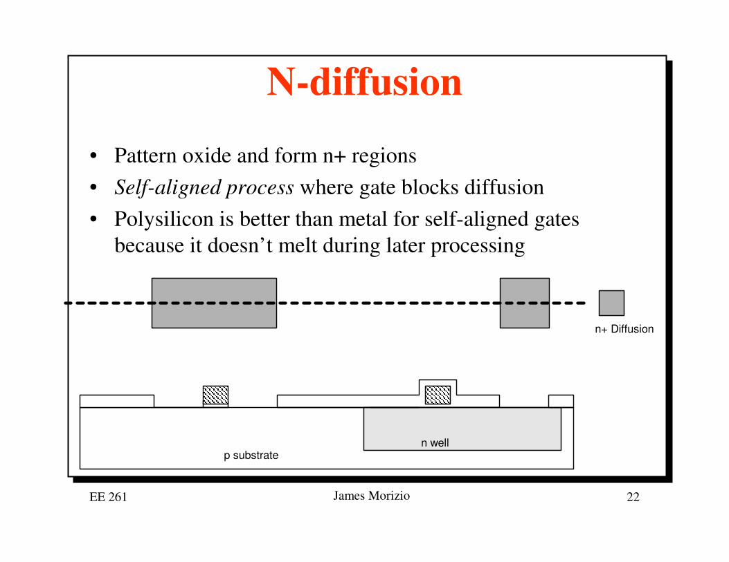
N-diffusion
• Pattern oxide and form n+ regions• Self-aligned process where gate blocks diffusion• Polysilicon is better than metal for self-aligned gates
because it doesn’t melt during later processing
p substraten well
n+ Diffusion
EE 261 James Morizio 23
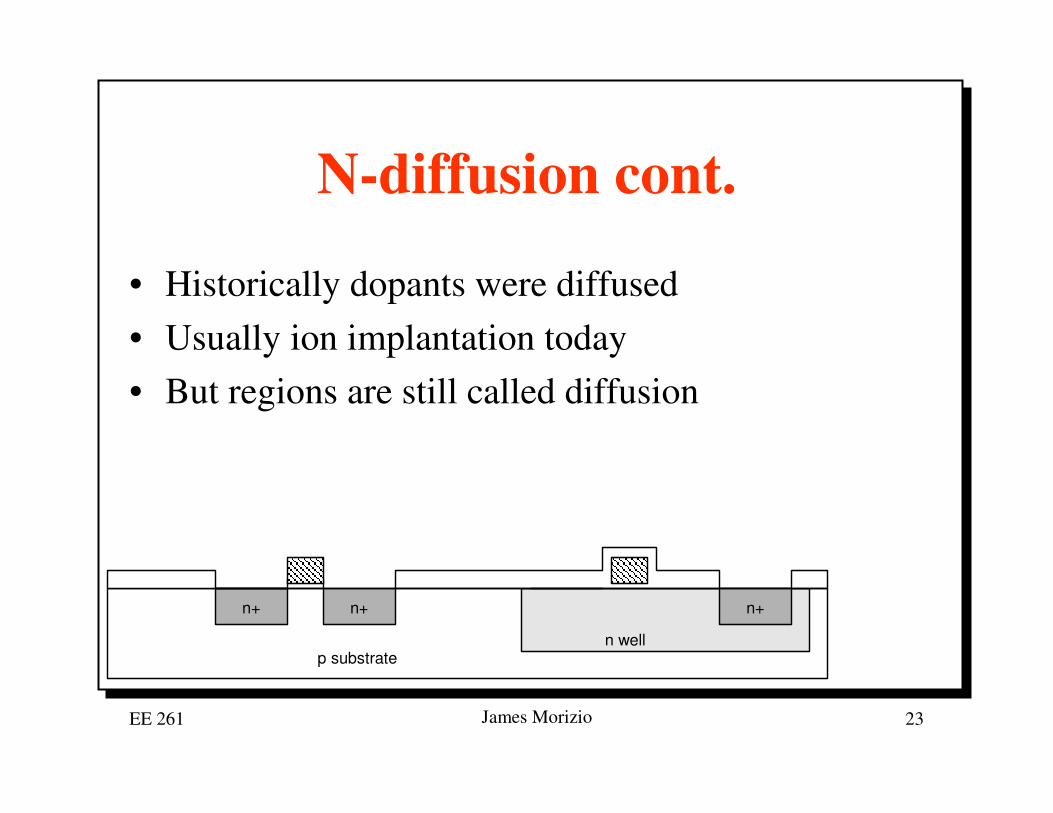
N-diffusion cont.
• Historically dopants were diffused• Usually ion implantation today• But regions are still called diffusion
n wellp substrate
n+n+ n+
EE 261 James Morizio 24
N-diffusion cont.
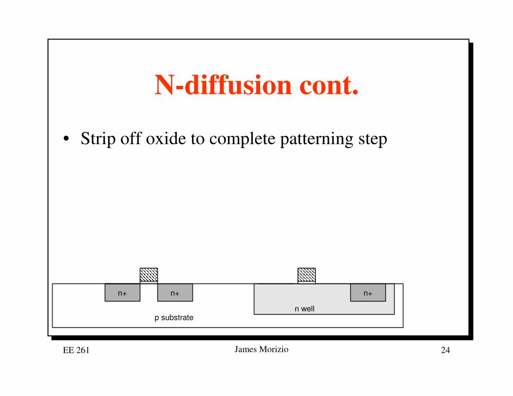
• Strip off oxide to complete patterning step
n wellp substrate
n+n+ n+
EE 261 James Morizio 25
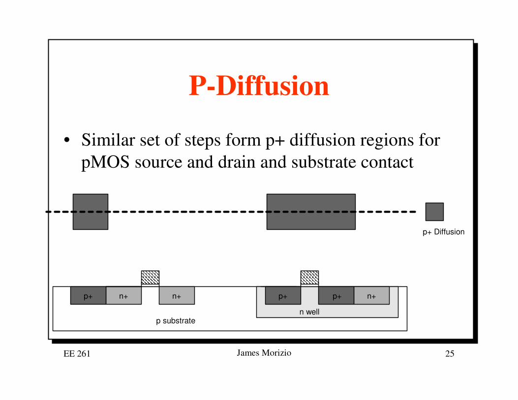
P-Diffusion
• Similar set of steps form p+ diffusion regions for pMOS source and drain and substrate contact
p+ Diffusion
p substraten well
n+n+ n+p+p+p+

EE 261 James Morizio 26
Contacts
• Now we need to wire together the devices• Cover chip with thick field oxide• Etch oxide where contact cuts are needed
p substrate
Thick field oxide
n well
n+n+ n+p+p+p+
Contact
EE 261 James Morizio 27
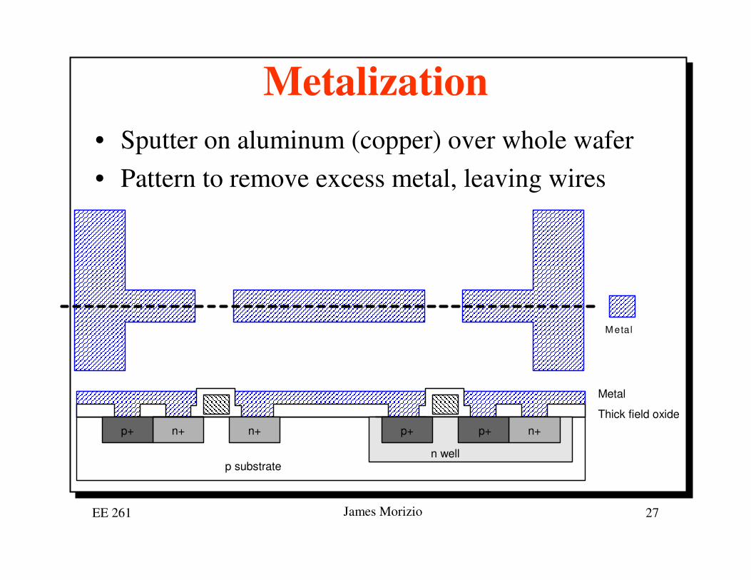
Metalization• Sputter on aluminum (copper) over whole wafer• Pattern to remove excess metal, leaving wires
p substrate
Metal
Thick field oxide
n well
n+n+ n+p+p+p+
M etal
EE 261 James Morizio 28
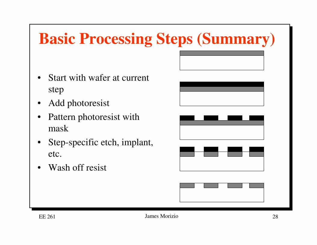
Basic Processing Steps (Summary)
• Start with wafer at current step
• Add photoresist• Pattern photoresist with
mask• Step-specific etch, implant,
etc.• Wash off resist
EE 261 James Morizio 29
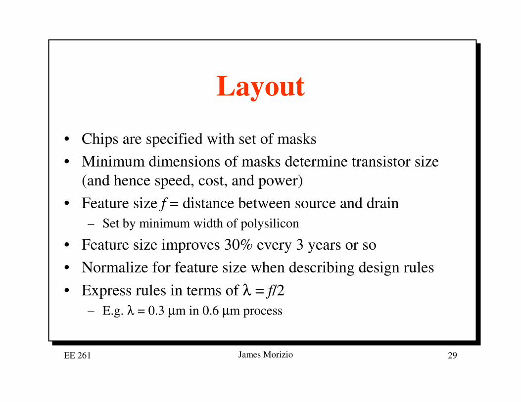
Layout
• Chips are specified with set of masks• Minimum dimensions of masks determine transistor size
(and hence speed, cost, and power)• Feature size f = distance between source and drain
– Set by minimum width of polysilicon
• Feature size improves 30% every 3 years or so• Normalize for feature size when describing design rules• Express rules in terms of λ = f/2
– E.g. λ = 0.3 µm in 0.6 µm process

EE 261 James Morizio 30
Design Rules• Design rules govern the layout of individual
components: transistors, wires, contacts, vias– How small can the gates be, and how small can the
wires be made?
• Conflicting Demands: – component packing: more functionality, higher speed– Chip yield: smaller sizes can reduce yield (fraction of
good chips)
• Conservative vs aggressive design rules
EE 261 James Morizio 31
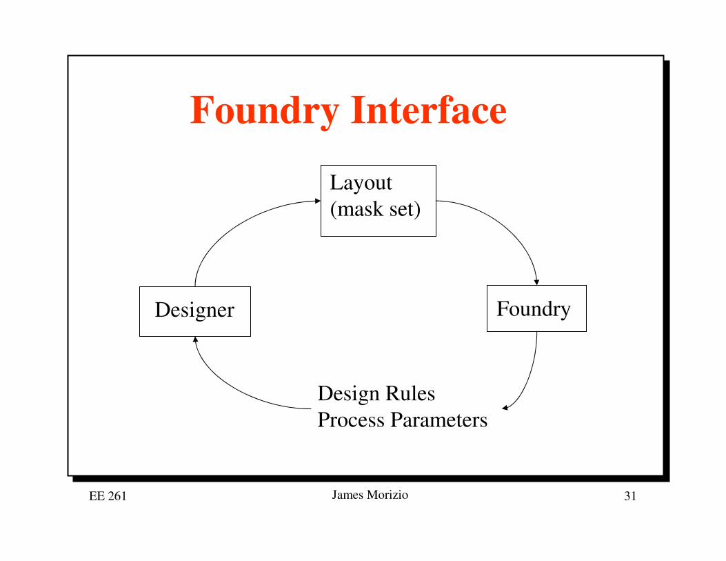
Foundry Interface
Designer
Layout(mask set)
Design RulesProcess Parameters
Foundry

EE 261 James Morizio 32
Geometric Design Rules
• Resolution– Width and spacing of lines on one layer
• Alignment– make sure interacting layers overlap (or don’t)– Contact surround– Poly overlap of diffusion– Well surround of diffusion

EE 261 James Morizio 33
SCMOS Design Rules• Scalable CMOS design rules• Feature size = half the drawn gate length (poly width)
• Mentor Graphics IC tool has built-in design rule checker (DRC)
Layer Minimum Width SeparationMetal 1 3 3Metal 2 3 4Poly 2 poly-poly: 2
poly-diff: 1
λ
λ
λ
λλ
λλ
λ
Example design rules:

EE 261 James Morizio 34
Simplified Design Rules
• Conservative rules to get you started
EE 261 James Morizio 35
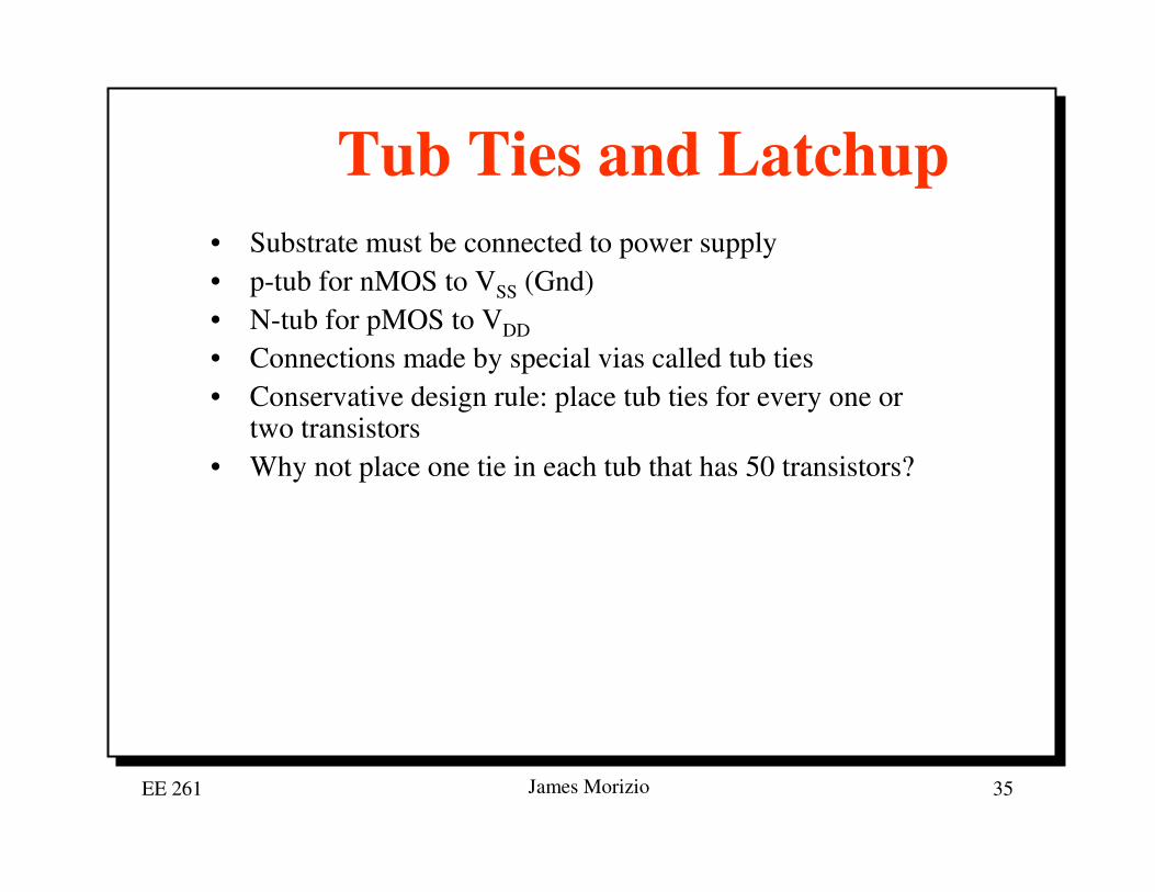
Tub Ties and Latchup• Substrate must be connected to power supply• p-tub for nMOS to VSS (Gnd)• N-tub for pMOS to VDD
• Connections made by special vias called tub ties• Conservative design rule: place tub ties for every one or
two transistors• Why not place one tie in each tub that has 50 transistors?

EE 261 James Morizio 36
Latchup• Too few ties: high resistance between tub and power supply, leads
to parasitic bipolar transistors inhibiting normal chip operation• Parasitic silicon-controlled rectifier (SCR)• When both bipolar transistors are off, SCR conducts no current• SCR turns on: high current short-circuit between VDD and Gnd.
(a) Origin of latchup (b) Equivalent circuit
VDD
Rpsubs
Rnwell p-source
n-source
n+ n+p+ p+ p+ n+
p-substrateRpsubs
Rnwell
VDD
n-well
EE 261 James Morizio 37
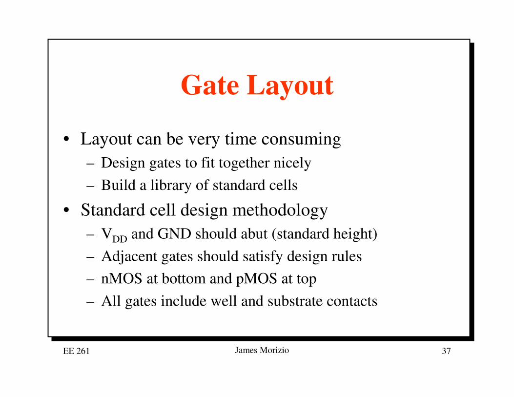
Gate Layout
• Layout can be very time consuming– Design gates to fit together nicely– Build a library of standard cells
• Standard cell design methodology– VDD and GND should abut (standard height)– Adjacent gates should satisfy design rules– nMOS at bottom and pMOS at top– All gates include well and substrate contacts
EE 261 James Morizio 38
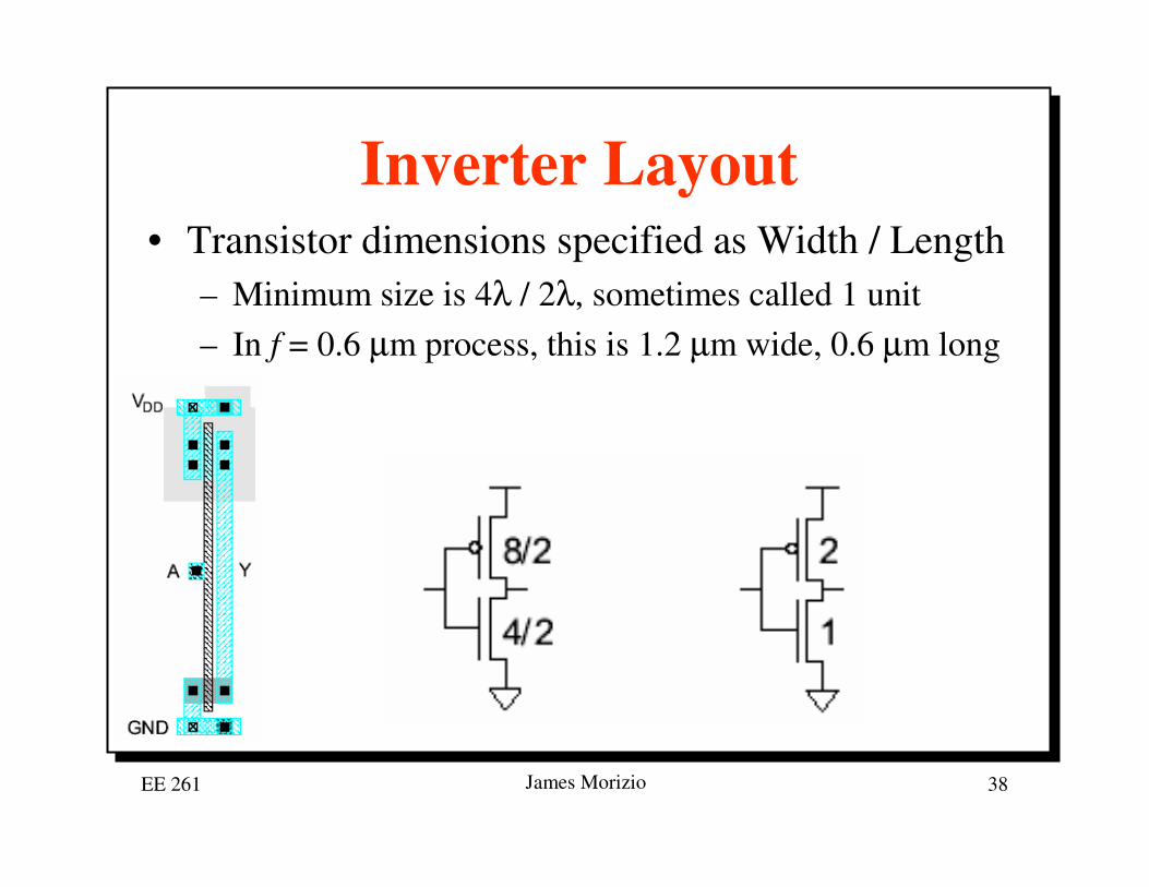
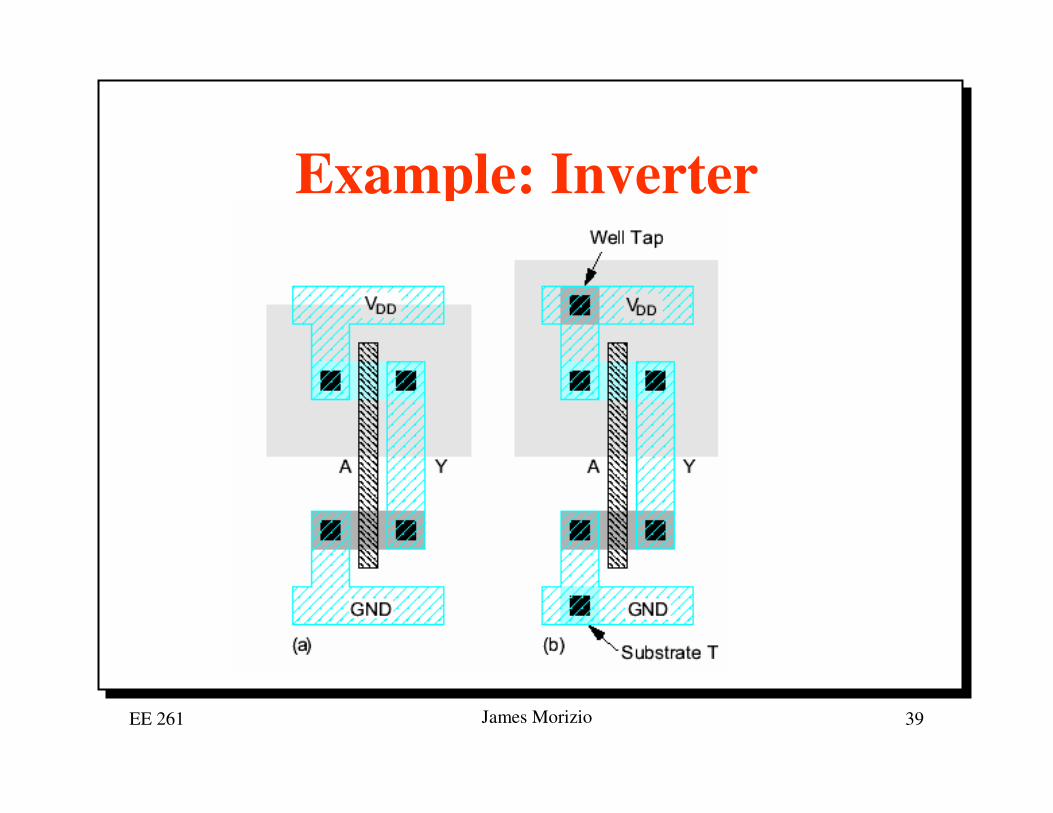
Inverter Layout• Transistor dimensions specified as Width / Length
– Minimum size is 4λ / 2λ, sometimes called 1 unit– In f = 0.6 µm process, this is 1.2 µm wide, 0.6 µm long
EE 261 James Morizio 39
Example: Inverter
EE 261 James Morizio 40
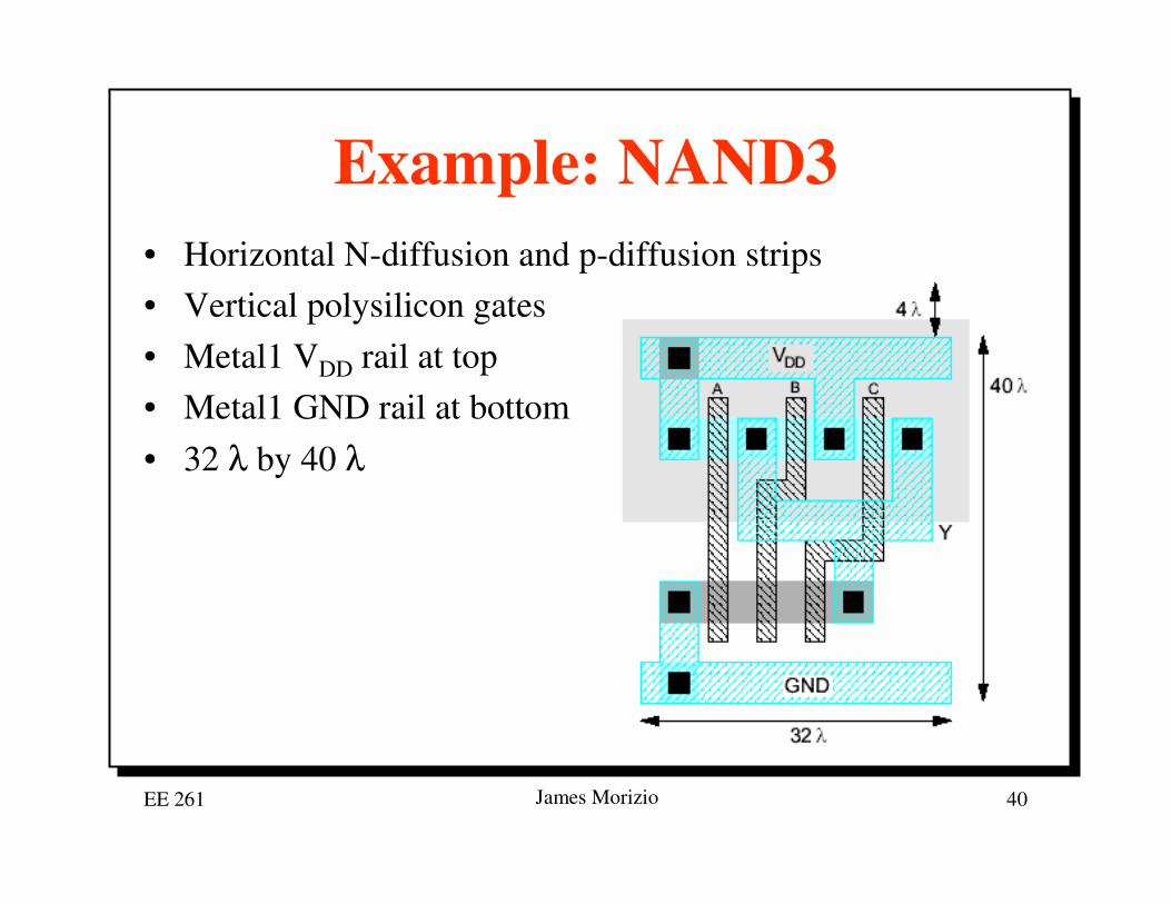
Example: NAND3• Horizontal N-diffusion and p-diffusion strips• Vertical polysilicon gates• Metal1 VDD rail at top• Metal1 GND rail at bottom• 32 λ by 40 λ

EE 261 James Morizio 41
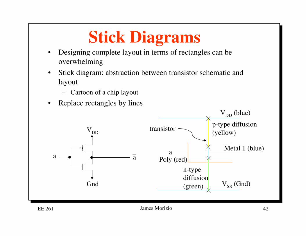
Stick Diagrams
• Stick diagrams help plan layout quickly– Need not be to scale– Draw with color pencils or dry-erase markers
EE 261 James Morizio 42
Stick Diagrams• Designing complete layout in terms of rectangles can be
overwhelming• Stick diagram: abstraction between transistor schematic and
layout– Cartoon of a chip layout
• Replace rectangles by lines
a a
VDD
Gnd
VDD (blue)
VSS (Gnd)
a
transistor
n-typediffusion(green)
Poly (red)
p-type diffusion(yellow)
Metal 1 (blue)
EE 261 James Morizio 43
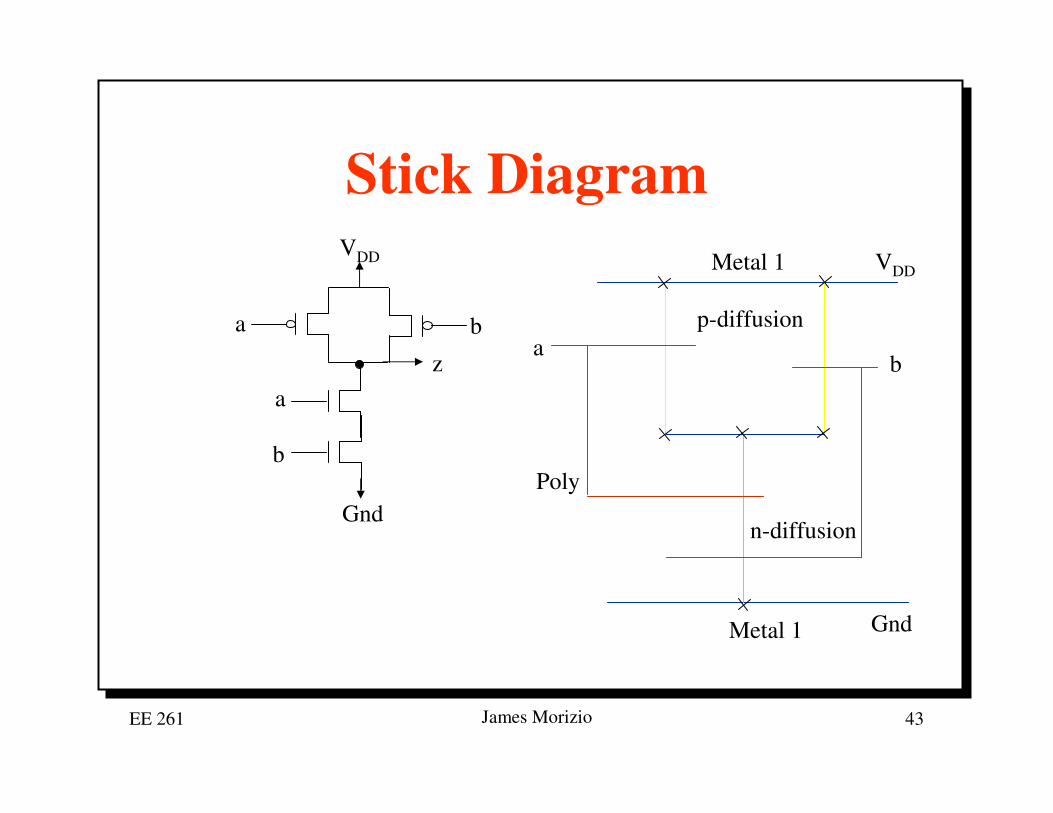
Stick Diagram
Gnd
VDD
a
b
a b
z
n-diffusion
p-diffusion
Metal 1
Metal 1
ab
Poly
VDD
Gnd
EE 261 James Morizio 44
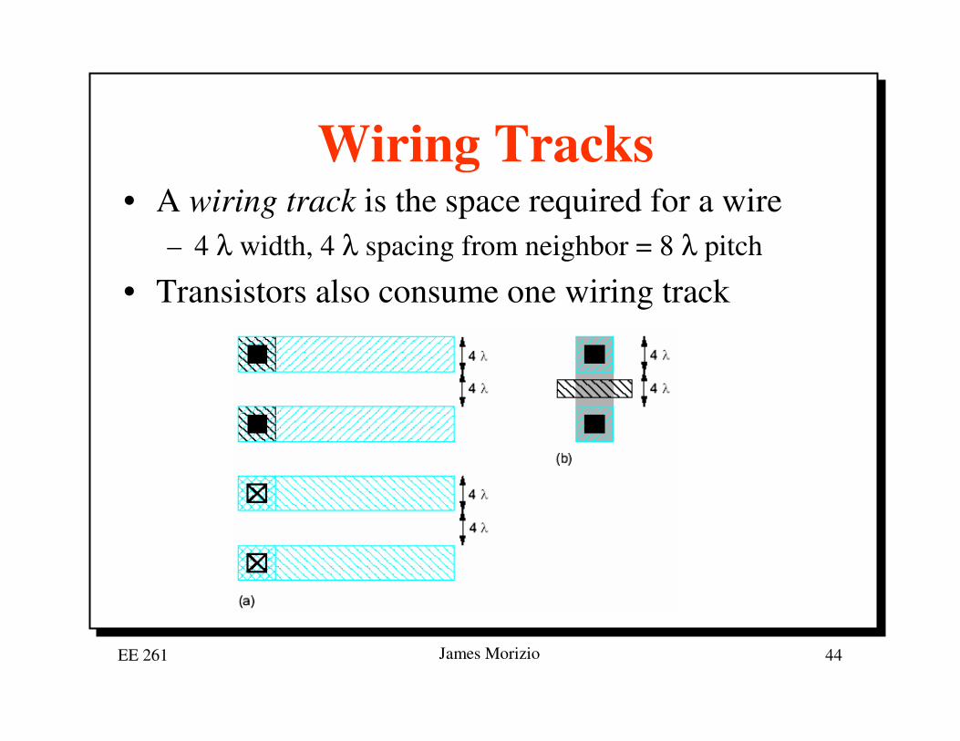
Wiring Tracks• A wiring track is the space required for a wire
– 4 λ width, 4 λ spacing from neighbor = 8 λ pitch
• Transistors also consume one wiring track
EE 261 James Morizio 45
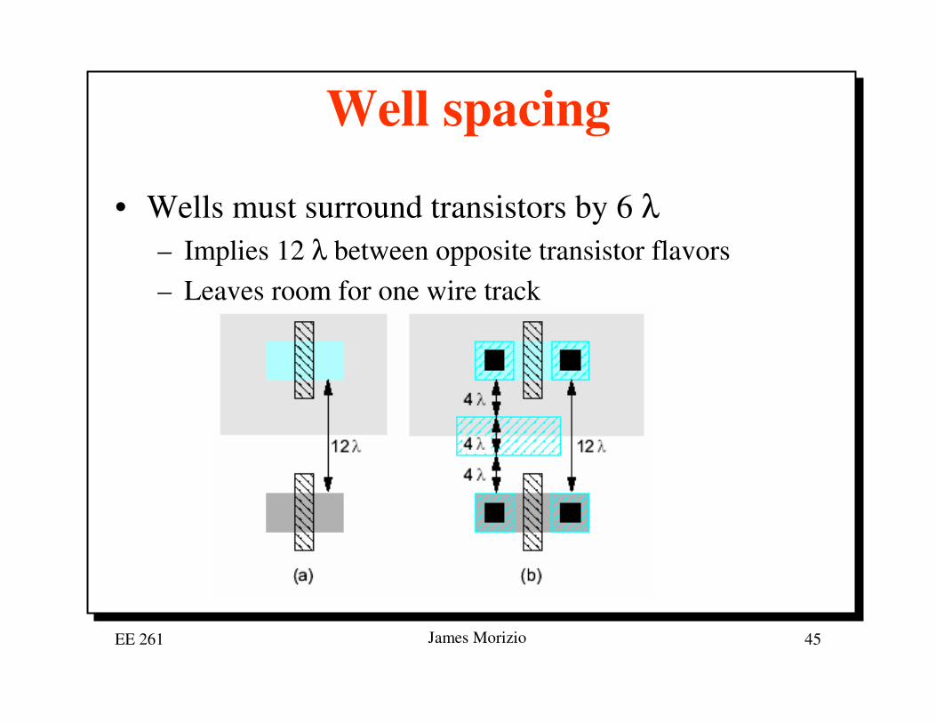
Well spacing
• Wells must surround transistors by 6 λ– Implies 12 λ between opposite transistor flavors– Leaves room for one wire track

EE 261 James Morizio 46
Area Estimation• Estimate area by counting wiring tracks
– Multiply by 8 to express in λ
EE 261 James Morizio 47
Example: O3AI
• Sketch a stick diagram for O3AI and estimate area– ( )Y A B C D= + + �
EE 261 James Morizio 48
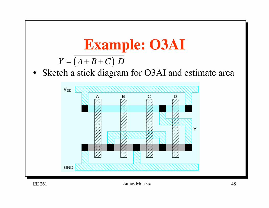
Example: O3AI
• Sketch a stick diagram for O3AI and estimate area( )Y A B C D= + + �
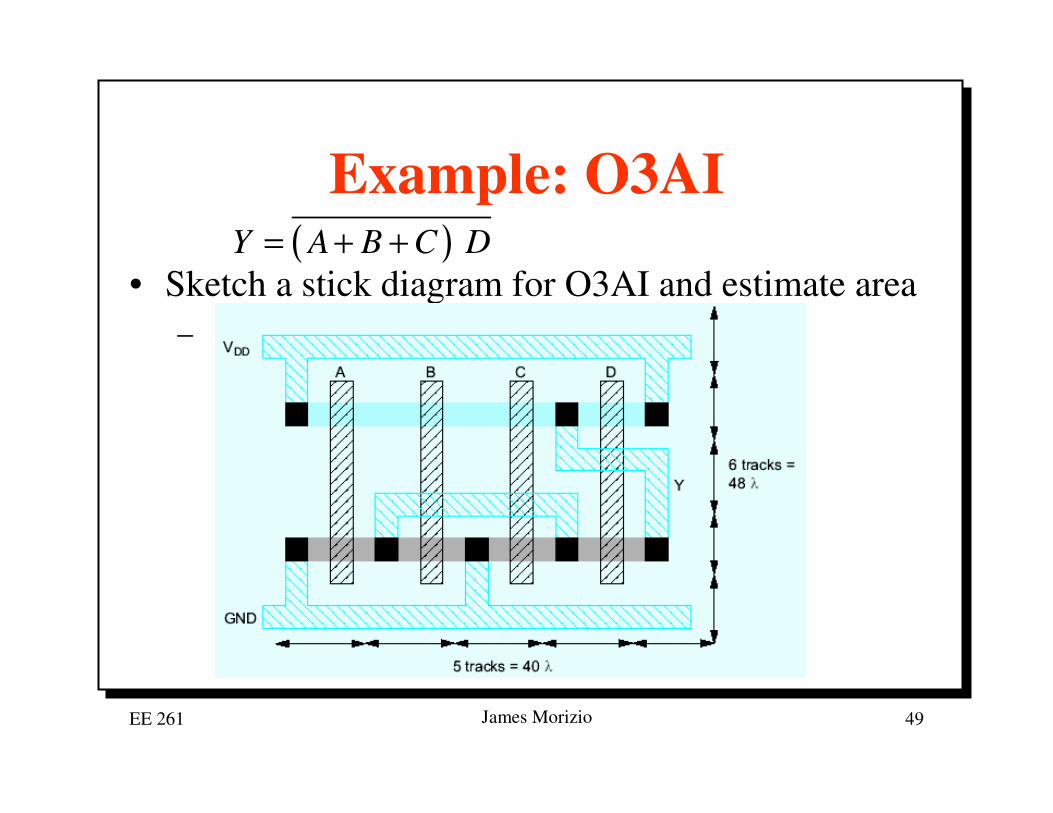
EE 261 James Morizio 49
Example: O3AI
• Sketch a stick diagram for O3AI and estimate area–
( )Y A B C D= + + �

EE 261 James Morizio 50
Some Layout Hints• Plan the global structure
(“big picture”), then design cells– Floorplan– Wiring strategy– Power and ground
distribution– Systematic placement– Keep all pMOS/nMOS
together– Place transistors in rows:
share source/drain diffusion
• Wiring on orthogonal metal layers– Assign preferred
directions to M1 and M2
– Use diffusion only for devices, not for interconnect
– Use poly only for very local interconnect

EE 261 James Morizio 51
Cell Minimization• Chip area (cell size) must be minimized carefully
Impact of die size/chip area on cost (unpackaged dies)
Wafer cost $1,460 $1,460 $1,460Die size 160.2 mm2 161.8 mm2 184.2 mm2
Die cost $84.06 $85.33 $102.55Chipsfabricatedper week 498.1 K 482.9 K 337.5 K Addedannual cost $63.5 M $961 M
NominalPentium die
1% increasein die size
15% increasein die size
1% increase in die size leads to 3%decrease in stock price for Intel!
EE 261 James Morizio 52
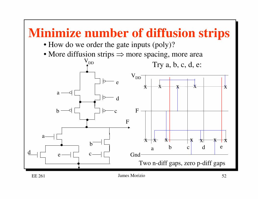
Minimize number of diffusion strips• How do we order the gate inputs (poly)?• More diffusion strips � more spacing, more area
VDD
ab
c
a
F
d e
b c
d
eVDD
Gnd
Try a, b, c, d, e:
a b c d ex xx
F
x x xx
x xx
Two n-diff gaps, zero p-diff gaps
x x

EE 261 James Morizio 53
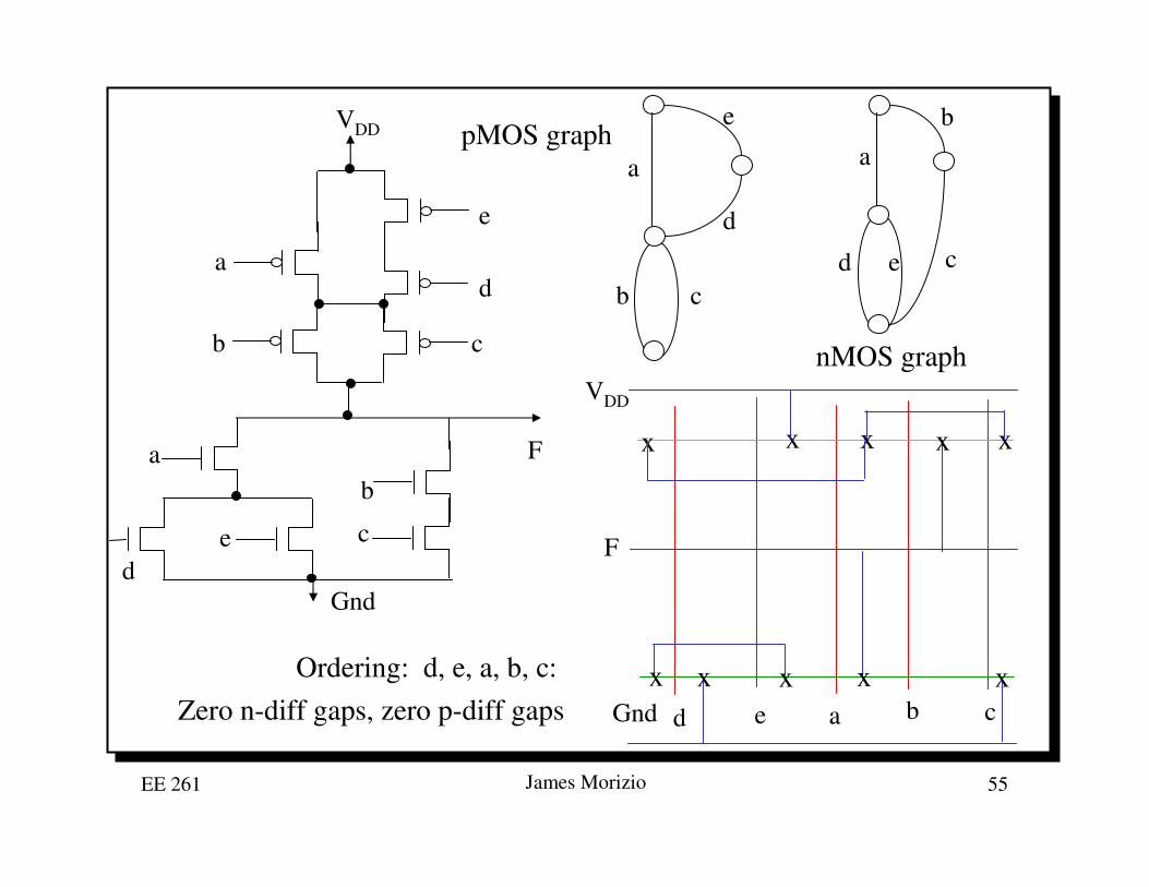
VDD
ab
c
a
Gnd
d e
b c
d
e
pMOS graph
a
b c
d
e
nMOS graph
b
c
a
d e
EE 261 James Morizio 54
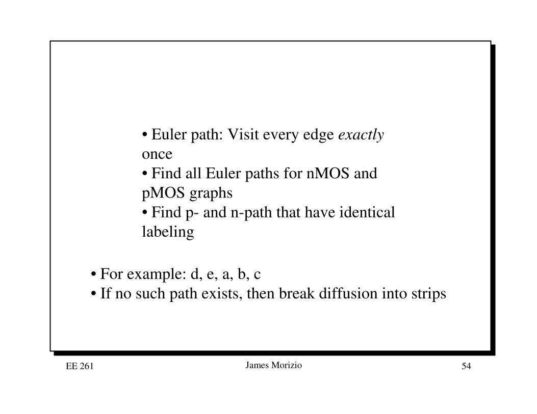
• Euler path: Visit every edge exactlyonce• Find all Euler paths for nMOS and pMOS graphs• Find p- and n-path that have identicallabeling
• For example: d, e, a, b, c • If no such path exists, then break diffusion into strips
EE 261 James Morizio 55
VDD
ab
c
a
Gnd
e
b c
d
e
pMOS grapha
b c
d
e
nMOS graph
b
c
a
d e
F
Ordering: d, e, a, b, c:
a b cd e
F
xx
VDD
GndZero n-diff gaps, zero p-diff gaps
d
x x x x
xx x
x

EE 261 James Morizio 56
Summary
• MOS Transistors are stack of gate, oxide, silicon• Can be viewed as electrically controlled switches• Build logic gates out of switches• Draw masks to specify layout of transistors
• Now you know everything necessary to start designing schematics and layout for a simple chip!