studies on organic solar cells based on small-molecules
TRANSCRIPT

Studies on Organic Solar Cells based on Small-Molecules:
Tetraphenyldibenzoperiflanthene and fullerene C70
Thesis presented to obtain the qualification of Doctor from the Universitat Politècnica de Catalunya Sergi Galindo Lorente Director: Dr. Joaquim Puigdollers González
June 2015


Acta de qualificació de tesi doctoral
Curs acadèmic: 2014-2015
Nom i cognoms
Sergi Galindo Lorente Programa de doctorat
Doctorat d’Enginyeria Electrònica
Unitat estructural responsable del programa Departament d’Enginyeria Electrònica
Resolució del Tribunal Reunit el Tribunal designat a l'efecte, el doctorand / la doctoranda exposa el tema de la seva tesi doctoral titulada
Studies on Organic Solar Cells based on Small-Molecules: Tetraphenyldibenzoperiflanthene and fullerene C70
_________________________________________________________________________________________.
Acabada la lectura i després de donar resposta a les qüestions formulades pels membres titulars del tribunal, aquest
atorga la qualificació:
NO APTE APROVAT NOTABLE EXCEL·LENT
(Nom, cognoms i signatura) President/a
(Nom, cognoms i signatura) Secretari/ària
(Nom, cognoms i signatura) Vocal
(Nom, cognoms i signatura) Vocal
(Nom, cognoms i signatura) Vocal
______________________, _______ d'/de __________________ de _______________
El resultat de l’escrutini dels vots emesos pels membres titulars del tribunal, efectuat per l’Escola de Doctorat, a
instància de la Comissió de Doctorat de la UPC, atorga la MENCIÓ CUM LAUDE:
SÍ NO
(Nom, cognoms i signatura)
President de la Comissió Permanent de l’Escola de Doctorat
(Nom, cognoms i signatura)
Secretari de la Comissió Permanent de l’Escola de Doctorat
Barcelona, _______ d'/de ____________________ de _________


“Serem allò que vulguem ser”
Miquel Martí i Pol


A Estefanía
A la meva família i amics
A la iaia Carmen


ix
Agraïments
És un plaer per mi expressar el meu agraïment a les moltes persones que han fet possible la
realització d’aquesta tesi. Em sento molt afortunat de la gran quantitat de persones que m’han fet
costat durant aquesta etapa.
En primer lloc, vull agrair al meu director de tesi Dr. Joaquim Puigdollers. Es diu que un
professor es fa responsable d’ensenyar-te; d’altra banda un mestre ensenya un camí per aprendre
i desenvolupar un coneixement sobre allò que desconeixes. Les lliçons de mestre que m’has
donat són, sens dubte, el més valuós d’haver fet la tesi. Gràcies també per introduir-me en el
món de la investigació. També per la teva paciència i motivació.
Al Prof. Ramón Alcubilla, responsable de la sala blanca i director del Centre de Nanoenginyeria
(CRnE) de la Universitat Politècnica de Catalunya (UPC), pels teus consells i pel teu suport en
tot moment.
Al Dr. Cristóbal Voz per la teva paciència i les teves explicacions, sobretot sobre les diferents
recombinacions i models de les cèl·lules solars.
A Albert Marsal, per l’ajuda incondicional en tot moment. Les teves idees per solucionar
problemes tècnics i la teva col·laboració en la fabricació i mesura dels transistors orgànics han
estat vitals per aquesta tesi.
A Mehrad Ahmadpour per la teva intensa participació en la fabricació de moltes cèl·lules solars.
Les teves ganes il· lusió, junt amb la resta d’estudiants del grup de cèl·lules solars orgàniques:
Guillermo Gerling, Siti Winny, Mulugeta Ayele, Som Mahato.
A tota la resta de membres del grup de Micro i Nano Tecnologies (MNT) de la UPC,
particularment als meus companys i amics Dr. Alfredo Boronat, Arnau Coll, Dr. David
Hernández, Gema López...
Als tècnics del CRnE de la UPC: Dr. Trifon Trifonov i Dr. Montse Domínguez; així com als
tècnics de la sala blanca de la UPC: Miguel García i Xavier Fermín per la seva col·laboració en
tot moment perquè tot funcioni correctament.
Al Grup d’Energia Solar del Departament de Física Aplicada i Òptica de la Universitat de
Barcelona, particularment a Dr. José Miguel Asensi, Dr. Joan Bertomeu, Dr. Aldrin Antony, Dr.
Paz Carreras i Dr. Rubén Roldán.

x
Al Prof. M.K. Jayaraj i a Vikas L S i a la resta del grup Nanophotonic & Optoelectronic Devices
Laboratory del Department of Physics de la Cochin University of Science and Technology
(CUSAT) per la vostra col·laboració i la seva bona acollida durant la meva estada a la Índia.
A les Dr. Stephanie Cheylan i Dr. Mónica della Pirriera per la vostra bona acollida i els seus
consells durant els meus primers dies al laboratori.
Al Dr. César Moreno per les teves profitoses discussions científiques.
Al Dr. Stamatis Georgakopoulos per les teves explicacions dels transistors i per llegir-te bona
part de la tesi. A Francesc Bejarano per la seva lectura crítica sobre els conceptes de química
orgànica. A la resta del grup NANOMOL del Institut de Ciència de Materials de Barcelona, pel
vostre suport durant l’escriptura de la tesi.
A Dr. Marta Mas pel teu suport i paciència mentre he estat escrivint la tesi.
A la tota la meva família, als meus pares, Màxim i Carme, a la meva germana Marina i el meu
germà Màxim, a la meva tieta Marga pel vostre suport incondicional. Gràcies Màxim per la teva
motivació científica i l’ajuda en l’edició de la tesi.
A Estefanía. M’has acompanyat tota la tesi. Ningú millor que tu sap el que ha costat. Ningú ho
ha patit tant. Gràcies.
Moltes gràcies a tots!

xi
Resum
En aquesta tesi s’investiguen cèl·lules solars orgàniques basades en semiconductors de petita
molècula. En particular, les cèl·lules solars orgàniques d’aquesta tesi han emprat
tetraphenyldibenzoperiflanthene com material donador i ful·lerè C70 com material acceptador.
En la primera part d'aquesta tesi, ens centrem en la influència de la densitat d'estats de la capa
donadora en els paràmetres característics de les cèl·lules solars. Més endavant, es presenten
cèl·lules solars orgàniques amb una estructura p-i-n, on la capa intrínseca s'obté per l'evaporació
conjunta del donador i l’acceptador. S'analitza la influència del gruix de la capa intrínseca de la
cèl·lula solar p-i-n en la característica de la cèl·lula solar.
En la segona part, es presenta un circuit equivalent per a les cèl·lules solars orgàniques. S'afegeix
un nou terme en el model estàndard que representa les pèrdues de recombinació a la capa activa
del dispositiu. L’anàlisi de les característiques de corrent – tensió mesurades a diferents
intensitats de llum permeten l'estimació del terme de recombinació. El model separa clarament
les qüestions tecnològiques (resistències en sèrie i en paral·lel) dels efectes relacionats amb la
física del dispositiu (pèrdues de recombinació). També permet l’obtenció d’un producte de la
mobilitat - temps de vida efectiu a la capa activa del dispositiu a ser determinat, la caracterització
del seu estat de degradació.

xii

xiii
Abstract
This work deals with the research on organic solar cells based on small-molecules
semiconductors. In particular, organic solar cells of this thesis have been used
tetraphenyldibenzoperiflanthene as donor material and fullerene C70 as acceptor material.
In the first part of this thesis, we focus on the influence of the density of states of the donor layer
on the characteristic parameters of solar cells. Further, organic solar cells with p-i-n structure are
presented, where the intrinsic layer is obtained by coevaporation of donor and acceptor. The
influence of the thickness of the intrinsic layer on the p-i-n solar cell characteristic is analysed.
In the second part, an equivalent circuit for organic solar cells is presented. A new term is added
to the standard model representing recombination losses in the active layer of the device. The
analysis of the characteristics of current - voltage measured at different illumination intensities
allows the estimation of the term recombination. The model clearly separates technological
issues (series and parallel resistance) from effects related to the physics of the device
(recombination losses). It also allows obtaining an effective mobility-lifetime product in the
active layer of the device to be determined, characterising its state of degradation.

xiv

xv
Table of contents
1. Introduction ........................................................................................................ 1
1.1 Motivation ........................................................................................................................ 1
1.2 Objective of this Thesis .................................................................................................... 6
1.3 Structure of this Thesis ..................................................................................................... 7
2. Organic Semiconductors ................................................................................. 11
2.1 Introduction .................................................................................................................... 11
2.2 Molecular Orbital Theory ............................................................................................... 13
2.3 Optical properties ........................................................................................................... 16
2.4 Charge Carrier Transport ................................................................................................ 18
2.4.1 Determination of the charge carrier mobility ................................................................ 19
3. Organic Solar Cells .......................................................................................... 27
3.1 Solar Cells Characterisation ........................................................................................... 27
3.1.1 Current - Voltage characteristics .................................................................................. 27
3.1.2 Equivalent circuit for solar cell ..................................................................................... 30
3.1.3 Spectral Response of solar cell ..................................................................................... 32
3.2 Working principle of Photovoltaic Solar Cells............................................................... 33
3.3 Working principle of Organic Solar Cells ...................................................................... 36
3.3.1 Carrier Recombination .................................................................................................. 41
3.3.2 Parameters characteristics of Organic Solar Cells ........................................................ 43
3.4 Device architecture ......................................................................................................... 45

xvi
4. Materials and Experimental Methods ........................................................... 55
4.1 Materials ......................................................................................................................... 55
4.2 Experimental Methods ................................................................................................... 58
4.2.1 Fabrication process for Organic Solar Cells ................................................................. 66
4.2.2 Characterisation of Organic Solar Cells ....................................................................... 70
5. Organic Solar Cells based on DBP and fullerene C70 ................................... 77
5.1 Bilayer Solar Cells based on DBP and C70..................................................................... 77
5.1.1 Introduction ................................................................................................................... 77
5.1.2 Electrical Characterisation ............................................................................................ 80
5.1.3 Morphology analysis .................................................................................................... 83
5.2 Influence of the Density of States in the open circuit voltage ........................................ 85
5.2.1 Introduction ................................................................................................................... 85
5.2.2 Mobility and density of states of donor DBP ............................................................... 87
5.3 p-i-n Organic Solar Cells based on DBP:C70 ................................................................. 91
6. Model for charge carrier collection efficiency in Organic Solar Cells ..... 101
6.1 Model for Organic Solar Cell ....................................................................................... 101
6.2 Introduction to the Variable Illumination Measurement method ................................. 102
6.2.1 Parameters of the model ............................................................................................. 103
6.2.2 Assumptions for the model ......................................................................................... 105
6.2.3 Effective mobility-lifetime product (μτeff) of charge carriers ..................................... 106
6.3 Results for p-i-n small-molecule solar cells based on DBP/C70 ................................... 108
6.4 Degradation of p-i-n Organic Solar Cells..................................................................... 110
7. Conclusions and Outlook ............................................................................... 115
APPENDIX I: Electrical Characterisation of Organic Semiconductors from
OTFT ..................................................................................................................... 117
A_I.1 Introduction ................................................................................................................... 117
A_I.2 Fabrication of OTFT ..................................................................................................... 118
A_I.3 Characterisation of OTFT ............................................................................................. 120
A_I.3.1 Determination of Mobility μ ................................................................................... 120
A_I.3.2 Determination of Density of States (DOS) ............................................................. 122

xvii
List of figures
Figure 1.1 - Evolution of record cell efficiencies of different solar cell technologies .................... 3
Figure 1.2 - Evolution of efficiencies from emerging solar cells .................................................... 5
Figure 2.1 - Chemical structures of polymers most used in organic solar cells. ........................... 12
Figure 2.2 - Chemical structures of small-molecules most used in organic solar cells. ............... 12
Figure 2.3 - Hybridization sp3. ...................................................................................................... 13
Figure 2.4 - Hybridization sp2 ....................................................................................................... 14
Figure 2.5 - Energetic diagram of molecular orbitals of an ethylene molecule ............................ 14
Figure 2.6 - Scheme of electron delocalization in a benzene ring. ............................................... 15
Figure 2.7 - Absorption coefficients in a variety of semiconductor materials at 300K ................ 17
Figure 3.1 - J–V curve of a PV cell under illumination conditions. .............................................. 28
Figure 3.2 - Spectral irradiance of the AM1.5 solar spectrum. ..................................................... 30
Figure 3.3 - Ideal solar cell ............................................................................................................ 31
Figure 3.4 - Equivalent circuit of a solar cell ................................................................................ 31
Figure 3.5 - Ideal structure of a photovoltaic device. .................................................................... 33
Figure 3.6 - Diagram showing the photogeneration in organic solar cell ..................................... 38
Figure 3.7 - Scheme of the creation of exciton and charge-transfer states. .................................. 40
Figure 3.8 - Electron thermalisation length (a) versus coulomb capture radius (rC). ................... 42
Figure 3.9 - The open circuit voltage in organic solar cells .......................................................... 43
Figure 3.10 - Diagram of single layer organic solar cell. .............................................................. 46

xviii
Figure 3.11 - Diagram of bilayer organic solar cell. ..................................................................... 46
Figure 3.12 - Diagram of Bulk Heterojunction organic solar cell. ............................................... 47
Figure 3.13 - Diagram of p-i-n organic solar cell ......................................................................... 48
Figure 3.14 - Diagram of tandem organic solar cell. .................................................................... 49
Figure 4.1 - Structure of Tetraphenyldibenzoperiflanthene (DBP) .............................................. 55
Figure 4.2 - Structure of fullerene C70 .......................................................................................... 56
Figure 4.3 - Schematic energy-level diagrams of several transition metal oxides ...................... 57
Figure 4.4 - Chemical structure of bathocuproine (BCP). ............................................................ 58
Figure 4.5 - Organic Evaporator UNIVEX 300 ............................................................................ 60
Figure 4.6 - Glovebox MB200B from MBraun ............................................................................ 61
Figure 4.7 - Top view of organic evaporation sources ................................................................. 61
Figure 4.8 - Schematic of organic chamber connections .............................................................. 62
Figure 4.9 - Glovebox MB200B from MBraun with our home-made organic evaporator ........... 62
Figure 4.10 - Purification of CuPc molecules. .............................................................................. 63
Figure 4.11 - Cross-beam workstation Zeiss Neon 40 .................................................................. 64
Figure 4.12 - Atomic Force Microscope Dimension 3100 Nanoman from Veeco ....................... 65
Figure 4.13 - UV-visible-NIR Spectrometer. Shimadzu 3600...................................................... 65
Figure 4.14 - Veeco DEKTAK 150 .............................................................................................. 66
Figure 4.15 - Geometry of ITO patterned substrate. ..................................................................... 68
Figure 4.16 - Alumina boat ........................................................................................................... 68
Figure 4.17 - MB-EcoVap ............................................................................................................ 69
Figure 4.18 - Shadow metal mask for evaporation ....................................................................... 69
Figure 4.19 - Cross-section of organic solar cell. ......................................................................... 70
Figure 4.20 - Prototype to measure organic solar cells in nitrogen atmosphere. .......................... 71
Figure 4.21 - Solar simulator Newport Oriel Model 94061A Class ABB. ................................... 71
Figure 4.22 - Spectral output of Solar Simulator with standard AM1.5G filter. .......................... 72
Figure 4.23 - Quantum efficiency integrated system. ................................................................... 72

xix
Figure 4.24 - Image of characterisation setup for Variable Intensity Measurements. .................. 73
Figure 4.25 - Scheme of Variable Intensity Measurement. ........................................................... 73
Figure 5.1 - Energy levels of the different layers comprising the bilayer solar cell. .................... 79
Figure 5.2 - Current – Voltage measurements of bilayer cells ...................................................... 80
Figure 5.3 - Photovoltaic parameters of organic solar cells versus DBP substrate temperature. .. 81
Figure 5.4 - Optical density of the active layers used for the fabrication of bilayer solar cells. ... 82
Figure 5.5 - EQE of bilayer solar cells .......................................................................................... 83
Figure 5.6 - AFM images of DBP thin films deposited at different substrate temperatures ......... 83
Figure 5.7 - Roughness of DBP thin films as function of the substrate temperature. ................... 84
Figure 5.8 - XRD of DBP thin films deposited at different substrate temperature. ...................... 85
Figure 5.9 - Output characteristics of a DBP based OTFT with a SiO2 gate dielectric. ............... 87
Figure 5.10 - Hole mobility of DBP as a function of the substrate temperature. .......................... 88
Figure 5.11 - Transfer characteristics of a DBP based OTFT ....................................................... 89
Figure 5.12 - Density of states of DBP as function of the substrate temperature. ........................ 90
Figure 5.13 - Structure of p-i-n solar cell ...................................................................................... 92
Figure 5.14 - J–V Curves of p-i-n cells for different i-layer thickness. ........................................ 93
Figure 5.15 - Photovoltaic parameters of p-i-n organic solar cells versus i-layer thickness. ........ 94
Figure 5.16 - EQE curves of p-i-n solar cells with different i-layer thicknesses. ......................... 96
Figure 6.1 - Equivalent circuit for standard solar cell. ................................................................ 102
Figure 6.2 - Equivalent circuit for solar cell with recombination term. ...................................... 103
Figure 6.3 - J–V curve of a p-i-n solar cell .................................................................................. 104
Figure 6.4 - Five illumination levels used in the VIM method ................................................... 104
Figure 6.5 - Structure of p-i-n solar cell used for VIM analysis. ................................................ 108
Figure 6.6 - J -V curves for the p-i-n organic solar cells measured with VIM method .............. 109
Figure 6.7 - Evolution of series resistance of p-i-n solar cells based on DBP:C70 (1:1) ............. 111
Figure 6.8 - p-i-n solar cells based on DBP:C70 (1:1) performance parameters across 30 h. ..... 112

xx

xxi
List of abbreviations
AFM Atomic Force Microscopy AM Air Mass a-Si:H Hydrogenated amorphous silicon BCP Bathocuproine Bphen Bathophenanthroline c speed of light CdTe Cadmium Telluride CIGS Copper Indium Gallium Selenide c-Si crystalline silicon CT Charge Transfer CV Cyclic Voltammetry CZTS Copper Zinc Tin Sulphide DOS Density-Of-States DSSC Dye-Sensitized Solar Cells
EEX binding exciton Eg energy band gap
EP energy of a photon EQE External Quantum Efficiency ETL Electron Transport Layer FET Field Effect Transistor FF Fill Factor FIB Focused Ion Beam h Planck’s constant HIT Heterojunction with Intrinsic Thin layer HOMO Highest Occupied Molecular Orbital HTL Hole Transport Layer IP Ionization Potential IPES Inverse Photoemission Spectroscopy IQE Internal Quantum Efficiency
ISD current between source and drain ITO Indium Tin Oxide J current density

xxii
J0 reverse bias saturation current density
JPH photocurrent generated per unit area
JSC Short circuit current density
kB Boltzmann constant
LD exciton diffusion length LUMO Lowest Unoccupied Molecular Orbital
MoO3 Molybdenum Oxide MTR Multiple Trapping and Release model N diode ideality factor OD Optical Density OLED Organic Light Emitting Diode OSC Organic Solar Cell OTFT Organic Thin Film Transistor
P0 incident illumination power Q elementary charge QD Quantum Dot RF–ID Radio Frequency - Identification Tag
RP parallel resistance
RS series resistance SCLC Space Charge Limited Current SEM Scanning Electron Microscope SR spectral response T Transmission TEM Transmission Electron Microscopy TMO Transition Metal Oxide TOF Time of flight UPS Ultraviolet Photoelectron Spectroscopy V applied voltage
VG gate voltage VIM Variable Illumination Measurement
VOC open circuit voltage
VSD Source-drain voltage
VT threshold voltage η power conversion efficiency
ηA photon absorption efficiency
ηCC carrier collection efficiency
ηCT charge transfer efficiency
ηED exciton diffusion efficiency µτ mobility-lifetime
τ0 lifetime of the exciton

1
1. Introduction
1.1 Motivation
Organic electronics is a division of materials science which deals with electrically-conductive
semiconductors based on polymers and small-molecules. It is called organic electronics because
these polymers and small-molecules are carbon-based. Organic electronics devices have attracted
much attention during last decades due to their potential advantages. Devices using organic
semiconductors should be cheaper and easier to manufacture than the corresponding ones based
on inorganic semiconductors. Among them, organic light emitting diodes (OLEDs) [1–2],
organic thin film transistors (OTFTs) [3–6] and organic solar cells (OSCs) [7–9] are rapidly
developing towards commercial applications.
OLEDs are used to create digital displays and lighting applications, in devices such as mobile
phones and portable digital media players, car radios and digital cameras among others. OTFTs
have already been demonstrated in applications like sensors [10–11], memory devices [12–13],
flexible displays [14–16] and radio frequency identification tags (RF–IDs) [17–18]. Another
application of organic semiconductors is in the field of photovoltaic solar cells, emerging as
alternative of traditional photovoltaic technologies. This thesis is focused on the interesting field
of solar cells based on organic semiconductors.
Today, the photovoltaic market is dominated by solar cells based on crystalline silicon.
Photovoltaics modules based on crystalline silicon present efficiencies on the order of 15–20%;
nevertheless it is the price what has pulling up this technology on top. Photovoltaic modules
based on crystalline silicon costs about 0.5–0.7 €/watt peak, making this technology competitive
with other renewable sources.
However, research laboratories are looking for new technologies that could lower down these
prices. The most promising technological alternatives are: thin films for photoactive layers and
solar concentrators. In addition, they are looking for products that could overcome some of the

Chapter 1 Introduction
2
limitations of crystalline silicon in terms of flexibility and weigh. In this sense, during the last
decade, many efforts have been focused on the fabrication of solar cells based on organic
semiconductors. Organic semiconductors can be processed at near ambient temperature over
large area, opening the possibility to fabricate large area devices on flexible substrates.
Light’s ability to generate electric current was first observed in 1839 by A. E. Becquerel when he
discovered the photoelectrochemical process [19]. Thenceforth, different technologies have
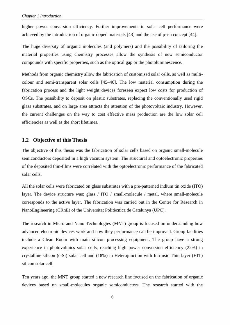
emerged in photovoltaic solar cells. Figure 1.1 shows the evolution of the best power conversion
efficiency for each solar cell technology during last decades.
The best efficiency reported for a monocrystalline silicon solar cell is 25% [20–21] getting quite
close to the “practical” limit of around 26% [22]. Although efficiencies of solar cells based on
monocrystalline silicon are very high, it is very important to keep an eye on solar cells based on
multicrystalline silicon, since today 5 out of 10 sold solar cells are manufactured using this
material. Multicrystalline silicon is cheaper than monocrystalline silicon, but unfortunately has
also a lower optoelectronic quality due to a higher amount of crystal defects and metal
impurities. Currently, the record efficiency in multicrystalline silicon solar cell is 20.4% [23].
Thin film solar cell is the alternative technology to the predominant crystalline silicon and its
market-share has been increasing in recent years to about 9% of worldwide photovoltaic
production in 2013 [24]. Thin-film technologies reduce the amount of active material in a cell,
having a film thickness from a few nanometres to tens of micrometers. Thin-film solar cells are
usually categorised by the photovoltaic material which they are made of. Cadmium Telluride
(CdTe), Copper Indium Gallium Selenide (CIGS) and hydrogenated amorphous silicon (a-Si:H)
are thin-film materials with long research tradition, and modules based on these materials are
well established. Currently, the module market prices of these technologies are quite similar and
slightly lower than c-Si solar modules, 0.46–0.63 €/watt peak. OSC, Dye-Sensitized Solar Cells
(DSSC) (this type of solar cell was invented by Michael Grätzel and Brian O’Regan [25] and are
also known as the Grätzel solar cell), Quantum Dot (QD) solar cells, Copper Zinc Tin Sulphide
(CZTS) solar cells have also emerged in the frame of thin film technology.

Figure 1.1 - Evolution of record cell efficiencies of different solar cell technologies. This graph is provided by the NREL (http://www.nrel.gov/ncpv/images/efficiency_chart.jpg
2-04-2015)

Chapter 1 Introduction
4
The last group of solar cells (OSC, DSSC, QD, and CZTS solar cells) belongs to what has been
called third generation solar cells. The physics behind their working principles are not well
established and some technological issues, mainly regarding its time stability, have limited its
influence to the research labs. Although some companies, such as DyeSol or Heliatek, start to
produce some of these solar cells (DSSC, OSC), their higher prices and poor stability, compared
to the crystalline silicon counterparts, has limited its wide spreading [26–27].
In 2014, researchers at the Zentrum für Sonnenenergie und Wasserstoff Forschung (ZSW) in
Stuttgart achieved a certified 21.7% conversion rate in a CIGS thin-film cell [28]. On the other
hand, the best CdTe solar cell efficiency has reached 21.5% by First Solar [29].
Recently, a new actor has made act of presence in the competitive world of solar cells
technologies: perovskites-based solar cells. A perovskite solar cell is a type of solar cell which
includes a perovskite structured compound, most commonly a hybrid organic-inorganic lead or
tin halide-based material, as the light-harvesting active layer. The properties that make this type
of solar cell very attractive are: controllable energy bandgap by the halide content [30–31] and
long diffusion length, for both holes and electrons, of over one micrometre [32]. Solar cell
efficiencies of devices using these materials have increased from 3.8% in 2009 [33] to 20.1%
achieved by the Korean Research Institute of Chemical Technology (KRICT) in 2014 [34],
making this the fastest advancing solar technology to date.
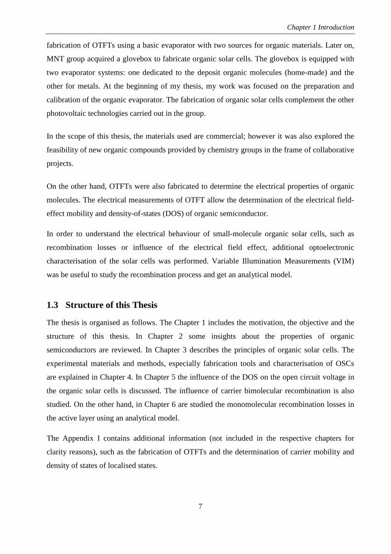
Figure 1.2 compare the evolution during last three decades of record efficiencies for various
promising third generation solar cells with the standard a-Si:H solar cells. Perovskites solar cells
efficiencies are also included. DSSC and a-Si:H solar cells (pink and blue curves) do not shown
significant improvement in power conversion efficiency during last two decades. Actually, the
best efficiency is 12.3% for DSSC obtained in laboratory by École Polytechnique Fédérale de
Lausanne (EPFL) [35] and 13.4% for a-Si:H solar cells reached by LG Electronics [23]. On the
other hand, the record power conversion efficiency of OSCs (red curve, for small area; and green
curve for larger than 1 cm2) have shown exponential increase, mainly since 2005. However, this
tendency seems to have stopped in 2012, when was reported the highest power conversion
efficiency of OSC with 12%, achieved by Heliatek Company and using triple tandem solar cell
geometry [36]. It is worth to mention that most of the research labs working on dye and organic
solar cells have shifted its activities to perovskites technology. This is especially true for dye
solar cells, since technology processes are quite similar for both technologies.

Chapter 1 Introduction
5
Figure 1.2 - Evolution of efficiencies from emerging solar cells (source: http://www.orgworld.de)
Traditionally, the study of semiconducting organic materials focused on small organic molecules
in the crystalline state, such as: anthracene, naphthalene or copper phthalocyanine [37–39].
Research activities were concentrated on phenomena associated with charge transport in
individual molecules; in general they showed poor semiconducting electrical characteristics, and
during many years few papers arise on this topic. However, this situation start to change when in
1977, Alan J. Heeger, Alan MacDiarmid and Hideki Shirakawa reported high electrical
conductivity in oxidized iodine-doped polyacetylene. They claimed that polyacetylene halides
could be the forerunners of a new class of organic polymers with electrical properties which may
be systematically and controllably varied over a wide range by chemical doping [40]. For this
research, they were awarded with the Nobel Prize in Chemistry in 2000 “for the discovery and
development of conductive polymers”. The breakthrough of the thin film organic solar cell was
made in 1986 by Ching Tang, when reported a power conversion efficiency of 1% [41]. Tang’s
cell comprises a bilayer structure of a donor and acceptor materials (copper phthalocyanine and
perylene tetracarboxylic derivative) and demonstrated that the properties in the interface region
are primarily responsible for the photogeneration of charges. The efficiencies of the reported
organic solar cells did not exceed 1% for many years. In 1992 Hiramoto et al. published the bulk
heterojunction solar cell by mixing donor and acceptor materials in a blend layer [42]. The use of
bulk heterojunction in active layer allowed a higher exciton dissociation and as a consequence
Chapter 1 Introduction
6
higher power conversion efficiency. Further improvements in solar cell performance were
achieved by the introduction of organic doped materials [43] and the use of p-i-n concept [44].
The huge diversity of organic molecules (and polymers) and the possibility of tailoring the
material properties using chemistry processes allow the synthesis of new semiconductor
compounds with specific properties, such as the optical gap or the photoluminescence.
Methods from organic chemistry allow the fabrication of customised solar cells, as well as multi-
colour and semi-transparent solar cells [45–46]. The low material consumption during the
fabrication process and the light weight devices foreseen expect low costs for production of
OSCs. The possibility to deposit on plastic substrates, replacing the conventionally used rigid
glass substrates, and on large area attracts the attention of the photovoltaic industry. However,
the current challenges on the way to cost effective mass production are the low solar cell
efficiencies as well as the short lifetimes.
1.2 Objective of this Thesis
The objective of this thesis was the fabrication of solar cells based on organic small-molecule
semiconductors deposited in a high vacuum system. The structural and optoelectronic properties
of the deposited thin-films were correlated with the optoelectronic performance of the fabricated
solar cells.
All the solar cells were fabricated on glass substrates with a pre-patterned indium tin oxide (ITO)
layer. The device structure was: glass / ITO / small-molecule / metal, where small-molecule
corresponds to the active layer. The fabrication was carried out in the Centre for Research in
NanoEngineering (CRnE) of the Universitat Politècnica de Catalunya (UPC).
The research in Micro and Nano Technologies (MNT) group is focused on understanding how
advanced electronic devices work and how they performance can be improved. Group facilities
include a Clean Room with main silicon processing equipment. The group have a strong
experience in photovoltaics solar cells, reaching high power conversion efficiency (22%) in
crystalline silicon (c-Si) solar cell and (18%) in Heterojunction with Intrinsic Thin layer (HIT)
silicon solar cell.
Ten years ago, the MNT group started a new research line focused on the fabrication of organic
devices based on small-molecules organic semiconductors. The research started with the
Chapter 1 Introduction
7
fabrication of OTFTs using a basic evaporator with two sources for organic materials. Later on,
MNT group acquired a glovebox to fabricate organic solar cells. The glovebox is equipped with
two evaporator systems: one dedicated to the deposit organic molecules (home-made) and the
other for metals. At the beginning of my thesis, my work was focused on the preparation and
calibration of the organic evaporator. The fabrication of organic solar cells complement the other
photovoltaic technologies carried out in the group.
In the scope of this thesis, the materials used are commercial; however it was also explored the
feasibility of new organic compounds provided by chemistry groups in the frame of collaborative
projects.
On the other hand, OTFTs were also fabricated to determine the electrical properties of organic
molecules. The electrical measurements of OTFT allow the determination of the electrical field-
effect mobility and density-of-states (DOS) of organic semiconductor.
In order to understand the electrical behaviour of small-molecule organic solar cells, such as
recombination losses or influence of the electrical field effect, additional optoelectronic
characterisation of the solar cells was performed. Variable Illumination Measurements (VIM)
was be useful to study the recombination process and get an analytical model.
1.3 Structure of this Thesis
The thesis is organised as follows. The Chapter 1 includes the motivation, the objective and the
structure of this thesis. In Chapter 2 some insights about the properties of organic
semiconductors are reviewed. In Chapter 3 describes the principles of organic solar cells. The
experimental materials and methods, especially fabrication tools and characterisation of OSCs
are explained in Chapter 4. In Chapter 5 the influence of the DOS on the open circuit voltage in
the organic solar cells is discussed. The influence of carrier bimolecular recombination is also
studied. On the other hand, in Chapter 6 are studied the monomolecular recombination losses in
the active layer using an analytical model.
The Appendix I contains additional information (not included in the respective chapters for
clarity reasons), such as the fabrication of OTFTs and the determination of carrier mobility and
density of states of localised states.

Chapter 1 Introduction
8
References
[1] C. W. Tang, S. A. VanSlyke, “Organic electroluminescent diodes”, Appl. Phys. Lett. 51 (1987) 913.
[2] J. H. Burroughes, D. D. C. Bradley, A. R. Brown, R. N. Marks, K. Mackay, R. H. Friend, P. L. Burns, A. B. Holmes. “Light-emitting diodes based on conjugated polymers”, Nature 347 (1990) 539.
[3] Y. Yamashita, “Organic semiconductors for organic field-effect transistors”, Sci. Technol. Adv. Mater. 10 (2009) 024313.
[4] C. D. Dimitrakopoulos, P. R. L. Malenfant, “Organic Thin Film Transistors for Large Area Electronics”, Adv. Mater. 14 (2002) 99.
[5] H. Klauk, “Organic thin-film transistors”, Chem. Soc. Rev. 39 (2010) 2643.
[6] C. Reese, M. Roberts, M. Ling, Z. Bao, “Organic thin film transistors”, Mater. Today 7 (2004) 20.
[7] P. Peumans, S. Uchida, S. R. Forrest, “Efficient bulk heterojunction photovoltaic cells using small-molecular-weight organic thin films” Nature 425 (2003) 158.
[8] F. C. Krebs, “Fabrication and processing of polymer solar cells: A review of printing and coating techniques”, Sol. Energy Mater. Sol. Cells 93 (2009) 394.
[9] H. Hoppe, N. S. Sariciftci, “Organic solar cells: An overview”, J. Mater. Res. 19 (2004) 1924.
[10] Z.-T. Zhu, J. T. Mason, R. Dieckmann, G. G. Malliaras, “Humidity sensors based on pentacene thin-film transistors”, Appl. Phys. Lett. 81 (2002) 4643.
[11] B. K. Crone, A. Dodabalapur, R. Sarpeshkar, A. Gelperin, H. E. Katz, Z. Bao, “Organic oscillator and adaptive amplifier circuits for chemical vapor sensing”, J. Appl. Phys. 91 (2002) 10140.
[12] S. J. Kim, J. S. Lee, “Flexible organic transistor memory devices”, Nano Lett. 10 (2010) 2884.
[13] M. Chang, P. Lee, S. P. McAlister, A. Chin, “A flexible organic pentacene nonvolatile memory based on high-k dielectric layers” Appl. Phys. Lett. 93 (2008) 233302.
[14] G. H. Gelinck, H. Edzer A. Huitema, E. van Veenendaal, E. Cantatore, L. Schrijnemakers, J. B. P. H. van der Putten, T. C. T. Geuns, M. Beenhakkers, J. B. Giesbers, B. Huisman, E. J. Meijer, E. M. Benito, F. J. Touwslager, A. W. Marsman, B. J. E. van Rens, D. M. de Leeuw, “Flexible active-matrix displays and shift registers based on solution-processed organic transistors”, Nat. Mater. 3 (2004) 106.
[15] L. S. Zhou, S. Park, B. Bai, J. Sun, S. C. Wu, N. J. Thomas, N. Shelby, F. Diane, Y. Hong, “Pentacene TFT driven AM OLED displays” IEEE Electr. Device L. 26 (2005) 640.
[16] M. Mizukami, N. Hirohata, T. Iseki, K. Ohtawara, T. Tada, S. Yagyu, T. Abe, T. Suzuki, Y. Fujisaki, Y. Inoue, S. Tokito, T. Kurita, “Flexible AM OLED panel driven by bottom-contact OTFTs”, IEEE Electr. Device L. 27 (2006) 249.

Chapter 1 Introduction
9
[17] W. Clemens, I. Fix, J. Ficker, A. Knobloch, A. Ullmann, “From polymer transistors toward printed electronics”, J. Mater. Res. 19 (2004) 1963.
[18] P. F. Baude, D. A. Ender, M. A. Haase, T. W. Kelley, D. V. Muyres, S. D. Theiss, “Pentacene-based radio-frequency identification circuitry”, Appl. Phys. Lett. 82 (2003) 3964.
[19] E. Becquerel, “Mémoire sur les effets électriques produits sous l'influence des rayons solaires”, C. R. Acad. Sci. 9 (1839) 561.
[20] M. A. Green, “The path to 25% silicon solar cell efficiency: History of silicon cell evolution”, Prog. Photovolt: Res. Appl. 17 (2009) 183.
[21] J. Zhao, A. Wang, M. A. Green, “24.5% Efficiency silicon PERT cells on MCZ substrates and 24.7% efficiency PERL cells on FZ substrates”, Prog. Photovolt: Res. Appl. 7 (1999) 471.
[22] R. M. Swanson, “Approaching the 29% limit efficiency of silicon solar cells”, Proceedings of the 31st IEEE Photovoltaic Specialists Conference, Orlando, USA (2005) 889.
[23] M. A. Green, K. Emery, Y. Hishikawa, W. Warta, E. D. Dunlop, “Solar cell efficiency tables (version 42)”, Prog. Photovolt: Res. Appl. 21 (2013) 827.
[24] Photovoltaics Report, Fraunhofer ISE, July 28 (2014) 18.
[25] B. O'Regan, M. Grätzel, “A low-cost, high-efficiency solar cell based on dye-sensitized colloidal TiO2 films”, Nature 353 (1991) 737.
[26] http://www.heliatek.com/newscenter/latest_news/heliatek-liefert-heliafilm-fuer-asiens-groesste-biopv-installation-in-singapur/?lang=en (02/05/2015).
[27] http://www.dyesol.com/partners/manufacturing-partners (02/05/2015).
[28] http://www.pv-tech.org/news/zsw_sets_21.7_cigs_cell_record (05/04/2015).
[29] http://investor.firstsolar.com/releasedetail.cfm?releaseid=864426 (05/04/2015).
[30] E. G. Eperon, S. D. Stranks, C. Menelaou, M. B. Johnston, L. M. Herz, H. J. Snaith, “Formamidinium lead trihalide: A broadly tunable perovskite for efficient planar heterojunction solar cells”, Energy Environ. Sci. 7 (2014) 982.
[31] J. H. Noh, S. H. Im, J. H. Heo, T. N. Mandal, S. I. Seok, “Chemical management for colorful, efficient, and stable inorganic-organic hybrid nanostructured solar cells”, Nano Lett. 13 (2013) 1764.
[32] S. D. Stranks, G. E. Eperon, G. Grancini, C. Menelaou, M. J. P. Alcocer, T. Leijtens, L. M. Herz, A. Petrozza, H. J. Snaith, “Electron-hole diffusion lengths exceeding 1 micrometer in an organometal trihalide perovskite absorber”, Science 342 (2013) 341.
[33] A. Kojima, K. Teshima, Y. Shirai, T. Miyasaka, “Organometal halide perovskites as visible-light sensitizers for photovoltaic cells”, J. Am. Chem. Soc. 131 (2009) 6050.
[34] http://www.photon.info/photon_news_detail_en.photon?id=90531 (05/04/2015).
Chapter 1 Introduction
10
[35] A. Yella, H. Lee, H. N. Tsao, C. Yi, A. K. Chandiran, M..K. Nazeeruddin, E. Wei-Guang Diau, C. Yeh, S. M Zakeeruddin, M. Grätzel, “Porphyrin-Sensitized Solar Cells with Cobalt (II/III)-Based Redox Electrolyte Exceed 12 Percent Efficiency”, Science 334 (2011) 629.
[36] “Heliatek consolidates its technology leadership by establishing a new world record for organic solar technology with a cell efficiency of 12%” (http://www.heliatek.com/wp-content/uploads/2013/01/130116_PR_Heliatek_achieves_record_cell_effiency_for_OPV.pdf) (22-02-2013).
[37] F. R. Lipsett, “On the production of single crystals of naphthalene and anthracene”, Can. J. Phys. 35 (1957) 284.
[38] T. Kajiwara, H. Inokuchi, S. Minomura, “Charge mobility of organic semiconductors under high pressure anthracene”, Bull. Chem. Soc. Jpn. 40 (1967) 1055.
[39] G. H. Heilmeier, G. Warfield, S. E. Harrison, “Applicability of the band model to metal-free phthalocyanine single crystals”, Phys. Rev. Letters 8 (1962) 309.
[40] H. Shirakawa, E. J. Louis, A. G. MacDiarmid, C. K. Chiang, A. J. Heeger, “Synthesis of electrically conducting organic polymers: Halogen derivatives of polyacetylene, (CH) x" J.C.S. Chem. Comm. 16 (1977) 578.
[41] C. W. Tang, “Two layer organic photovoltaic cell”, Appl. Phys. Lett. 48 (1986) 183.
[42] M. Hiramoto, H. Fujiwara, M. Yokoyama, “p-i-n like behavior in three-layered organic solar cells having a co-deposited interlayer of pigments”, J. Appl. Phys. 72 (1992) 3781.
[43] M. Pfeiffer, T. Fritz, J. Blochwitz, A. Nollau, B. Plönnigs, A. Beyer, K. Leo, “Controlled doping of molecular organic layers: Physics and device prospects”, Advances in Solid State Physics 39 (1999) 77.
[44] B. Maennig, J. Drechsel, D. Gebeyehu, P. Simon, F. Kozlowski, A. Werner, F. Li, S. Grundmann, S. Sonntag, M. Koch, K. Leo, M. Pfeiffer, H. Hoppe, D. Meissner, N. Sariciftci, I. Riedel, V. Dyakonov, J. Parisi, “Organic p-i-n solar cells”, Applied Physics A: Materials Science & Processing 79 (2004) 1.
[45] L. Wen, Q. Chen, F. Sun, S. Song, L. Jin, Y, Yu, “Theoretical design of multi-colored semi-transparent organic solar cells with both efficient color filtering and light harvesting”, Sci. Rep. 4 (2014) 7036.
[46] R. R. Lunt, V. Bulovic, “Transparent, near-infrared organic photovoltaic solar cells for window and energy-scavenging applications”, Appl. Phys. Lett. 98 (2011) 113305.

11
2. Organic Semiconductors In this chapter the basic chemical and physical properties of organic semiconductors are
introduced, as they are required for understanding the results presented in this thesis. First, the
formation of molecular orbitals theory is discussed. Later, electrical and optical properties of
organic semiconductors materials are described, as well as charge transport mechanism in
organic materials.
2.1 Introduction
Organic semiconductors are promising materials for organic electronics due to their favourable
properties, allowing them to be utilised in high throughput and low-cost fabrication methods.
Organic semiconductors are carbon-based compounds, usually also composed of other element
atoms such as oxygen, nitrogen or sulphur, with semiconducting properties. The commonly used
organic semiconductors can be categorised as oligomers (small-molecules) or conjugated
polymers. Small-molecules have low molecular weight; in contrast, polymers, at least in
principle, consist of a nearly unlimited number of repeatable monomers and have long molecular
chains. Figure 2.1 and Figure 2.2 depicts the most used as absorbers in organic photovoltaics.
An important difference between small-molecules and polymers lies in the way how they are
processed to form thin-films. Whereas small-molecules are usually deposited via thermal
evaporation or sublimation under ultra-high vacuum, conjugated polymer are generally deposited
using solution-processed methods, such as spin-coating, ink-jet printing or doctor blade
techniques.

Chapter 2 Organic Semiconductors
12
ZnPc
Fullerene C60
CuPc Pentacene
Fullerene C70 Tetraphenyldibenzoperiflanthene (DBP)
Figure 2.1 - Chemical structures of polymers most used in organic solar cells.
Figure 2.2 - Chemical structures of small-molecules most used in organic solar cells.

Chapter 2 Organic Semiconductors
13
Small-molecules are very attractive for application in solar cells because they have several
advantages versus polymers such as:
• Short synthesis: less than five steps are usually needed to synthesize the compound. Its
well-defined chemical structures make them synthetically well reproducible.
• Higher purity: small-molecule materials have well-defined molecular weights, allowing
for straightforward separation of the host from the impurities. They are easily purified by
re-crystallization and/or sublimation.
• Better control on the structure and morphology of the deposited film; depending on the
growth parameters (substrate temperature, pressure inside the deposition chamber and
deposition rate) the deposited film can be poly-crystalline or amorphous in nature.
• Solvents (potentially toxic) are not needed.
• Multilayer devices: The preparation of well-defined multilayer structures, such as tandem
solar cells, is comparatively easy because of the control of the layer thickness on the
nanometre scale.
2.2 Molecular Orbital Theory
There are a large number of binding configurations of carbon (several millions of compounds
were reported). A carbon atom has six electrons and its ground state configuration is 1s22s22p2,
where s orbitals are fully occupied and two of three px, py, pz orbitals are occupied by one
electron. When carbon atom makes a bond with another atom, hybridization occurs between s
and p orbitals. The hybridization sp3 occurs when a carbon atom connects via four single bonds
to other atoms by σ-bonds, such saturated compounds are good electrical insulators (Figure 2.3).
Examples of this binding configuration are alkanes, or saturated polymers such us
polyethylene - CH − CH -, polystyrene or polypropylene.
Figure 2.3 - Hybridization sp3.

Chapter 2 Organic Semiconductors
14
On the other hand, molecules containing double or triple bonds are more complex and interesting
from the point of view of the optical and electrical properties, for instance ethylene, H2C=CH2.
In this case carbon atoms exhibit a sp2 hybridization which means that one s orbital and two p
orbitals are combined. Figure 2.4 depicts sp2 hybridization.
Figure 2.4 - sp2-hybridization of the valence electrons of two carbon atoms lead to molecular π- and σ-bondings.
In each carbon atom, three sp2 hybrid orbitals are arranged in a trigonal planar geometry (120º
between them), while the non-hybridized 2pz remain perpendicular to this plane. The
combination of one sp2 orbital from each carbon atom gives two orbitals in the final molecule
known as σ and σ*. The side-by-side overlapping of both 2pz orbitals also results in two orbitals
in the final molecule: π and π*. These orbitals are ordered from lower energy to higher energy as
follows: σ, π, π*, σ*. The orbitals π and σ are filled with electrons and constitute the double bond
(stronger σ bond and weaker π bond). The energetically highest occupied molecular orbital is
called HOMO. On the other hand, the energetically lowest unoccupied molecular orbital is called
LUMO. Comparing to inorganic semiconductors, it should be noted that HOMO is the analogue
of valence band and LUMO is the analogue of conduction band. In the case of ethylene
molecule, the π orbital is the HOMO meanwhile the π* is the LUMO (Figure 2.5).
Figure 2.5 - Energetic diagram of molecular orbitals of an ethylene molecule

Chapter 2 Organic Semiconductors
15
The HOMO–LUMO is the lowest electronic transition. The difference between the π-π*
molecular orbital is called energy band gap (Eg) and confers the optoelectronical properties of a
semiconductor.
If the molecule presents an alternation of simple and double bonds over a planar segment the
system is said to be π-conjugated. This system can be presented in many forms, as well as small-
molecules, conjugated polymers or molecular crystals. For each double bond a new pair of π, π*
orbitals appear in the energetic diagram of orbitals of the final molecule, and the gap between
occupied and empty states in these π systems becomes smaller. In this kind of molecules, the
molecular orbitals, from lower to higher energy, are: σ,…, σn, π, …, πn, πn*, …, σn
*.
If carbon atoms form larger molecules, typically with benzene rings as the basic unit, the
HOMO–LUMO gap becomes so small that the HOMO electrons can overcome this energetic
barrier in such way that they do not belong to a single bond or atom, but rather to a group of
atoms. The π-bonds become delocalised and form a π-system which often has the extensions of
the molecule. Figure 2.6 depicts π-electrons moving along the conjugated chain as a flip-flop
between single and double bonds.
Figure 2.6 - Scheme of electron delocalization in a benzene ring.
The ionization potential (IP) is the minimum amount of energy required to extract an electron
from the molecule. On the other hand, the electron affinity (EA) is defined as the amount of
energy released when an electron is added to a molecule. In this work, we set HOMO equal to
the IP and the LUMO to the EA.
Chapter 2 Organic Semiconductors
16
Due to a small molecular interaction (overlapping of the π-orbitals) in the organic solid, the
charge carrier transport level for holes (HOMO) is only weakly broadened. The LUMO
corresponds to the electron transport level in organic solids.
The value of the HOMO level is often determined by means of cyclic voltammetry and
photoemission yield spectroscopy techniques, while the value of the LUMO level is usually
measured by cyclic voltammetry (CV) or calculated by adding up the measured HOMO level
and the measured optical bandgap. CV allows the estimation of the energetic levels from liquid
solutions; in contrast, the technique used to measure the HOMO level in thin films is ultraviolet
photoelectron spectroscopy (UPS) (or inverse photoemission spectroscopy (IPES) in the case of
the LUMO level).
2.3 Optical properties
Optical density (OD) is the amount of attenuation (or gradual intensity loss) that occurs when
light passes through an optical component. Optical attenuation may result from not only
absorption of light but also from scattering of light. Higher OD values indicate a higher level of
blocking. The OD can be calculated from optical transmission (T) measurements (Eq. 2.1):
The optical density of a material relates to the sluggish tendency of the atoms of a material to
maintain the absorbed energy of an electromagnetic wave in the form of vibrating electrons
before reemitting it as a new electromagnetic disturbance. When the material is more optically
dense a wave will move slowly through the material. The OD depends on the material and its
thickness.
On the other hand, the optical absorption coefficient (α) determines how far into a material light
of a particular wavelength can penetrate before it is absorbed. The absorption coefficient only
depends on the material and on the wavelength of light which is being absorbed. In a material
with a low absorption coefficient, light is only poorly absorbed, and if the material is thin
enough, it will appear transparent to that wavelength. Inorganic semiconductor materials have a
sharp edge in their absorption coefficient, since light which has energy below the band gap does
not have sufficient energy to excite an electron into the conduction band from the valence band.
Consequently this light is not absorbed. The absorption coefficient for hydrogenated amorphous
= − log (2.1)

Chapter 2 Organic Semiconductors
17
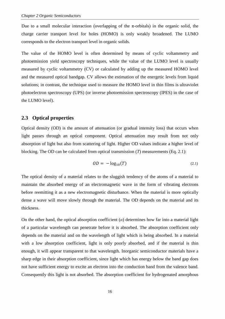
silicon (a-Si:H), crystalline silicon (c-Si) and pentacene semiconductors materials is shown
below (Figure 2.7).
1,0 1,5 2,010-1
100
101
102
103
104
105
a-Si:H c-Si pentacene
Energy (eV)
α (
cm-1 )
Figure 2.7 – Optical absorption coefficients for different thin film semiconductors.
The Figure 2.7 shows that, even for those photons which have energy above the band gap, the
absorption coefficient is not constant, but still depends strongly on wavelength. The probability
of absorbing a photon depends on the likelihood of having a photon and an electron interact in
such a way as to move from one energy band to another. For photons which have energy very
close to that of the band gap, the absorption is relatively low since only those electrons directly
at the valence band edge can interact with the photon to cause absorption. As the photon energy
increases, not just the electrons already having energy close to that of the band gap can interact
with the photon. Therefore, a larger number of electrons can interact with the photon and result
in the photon being absorbed.
The absorption coefficient, α, is related to the extinction coefficient, k, by the following formula:
= 4 (2.2)

Chapter 2 Organic Semiconductors
18
where λ is the wavelength. If λ is in nm, it is necessary to multiply by 107 to get the absorption
coefficient in units of cm-1.
Organic semiconductors are characterised by high absorption coefficients which make it possible
to manufacture thin film devices. The use of such thin layers reduces the amount of active
material required and also makes light-weight. In addition, this allows the production of flexible
devices, and even the realization of semitransparent solar cells which can be integrated into
windows and glass facades.
2.4 Charge Carrier Transport
Due to the weak electronic coupling in organic semiconductors, the charge carriers can be
effectively localised on a single molecule. Disordered molecular solids exhibit generally an
inhomogeneous energy distribution of their localised transport states. Therefore, the charge
carrier transport between adjacent molecules is thermally activated and the mobility increases
with increasing temperature [1]. This kind of thermally activated charge carrier transport is
known as hopping transport. The mobility due to thermally assisted hopping is many orders of
magnitude lower than that due to band transport. The charge transport mechanism via a localised
hopping mechanism is characterized by a radical ion that polarizes the surrounding neutral
molecules. The rate of this hopping process may be expressed with Marcus theory [2–3].
Sometimes the ensemble of localised states within a certain energy range is called band. It is
stated here, that the term band in this context has nothing to do with energy bands in an ideal
crystal.
In contrast, band-like conduction can occur in organic semiconductors if its structure is well
organised like in the case of organic crystals. Similar to inorganic semiconductors, the
conductivity in very pure and highly ordered organic solids is limited by scattering processes
with phonons [4]. In contrast to the hopping transport, the conductivity is increasing with
decreasing temperature due to a reduction of the respective scattering probability.
It can be summarized, that in well-organized organic crystals the charge transport is based on
polaron bands, while the hopping transport prevails in polycrystalline and amorphous materials.
Next, the most used charge transport models in organic semiconductors are briefly exposed.
However, it is important to note that a full comprehensive theory to describe the charge transport
in organic semiconductors is still lacking.

Chapter 2 Organic Semiconductors
19
Hopping Mechanism
A theory involving electron transfer based on oxidation – reduction reactions assuming very little
spatial overlap of the electronic orbitals of two reacting molecules was introduced by Marcus in
1956 [5]. The charge transport can be described as involving a self-exchange electron (hole)
transfer from a charged molecule to a next neutral one by hopping of charges. According to this
theory, two major parameters determine self-exchange rates [2] [6]:
i. the electronic coupling between adjacent molecules, which needs to be maximized.
ii. the reorganization energy, which needs to be small for efficient charge transport.
Here the reorganization energy corresponds basically to the sum of geometry relaxation energies
switching from the neutral state to the charged state and vice versa. All this elucidates the strong
importance of intermolecular interactions on the efficiency of charge carrier hopping and their
related mobility since they are directly related.
Multiple Trapping and Release Model
Introduced originally to description of the low mobility of hydrogenated amorphous silicon
devices [7], in the Multiple Trapping and Release (MTR) model the charge carriers are assumed
to travel in narrow, delocalised bands and interact with a high concentration of localised trap
levels. Further adapted by Horowitz et al. [8–9] the localised trap levels are believed to arise
from defects and impurities in both the molecular and crystal structure. In the decentralised band
the charge carriers have a band mobility µ0, but interact further by trapping and detrapping with
localised states. The trapping and release mechanisms determines the overall mobility and the
thermally activated behaviour. The trap distribution (Density of States (DOS) within the gap) is
believed to be exponentially shaped. Also, the often observed gate voltage, i.e. electric field,
dependence of the charge carrier mobility can be described with this model.
2.4.1 Determination of the charge carrier mobility
The charge carrier mobility characterises how quickly a charge can move through a metal or
semiconductor. The term carrier mobility refers in general to both electron and hole mobility in
semiconductors. The charge carrier mobility of an organic material can be determined from
different approaches. The charge carrier mobilities of organic materials greatly vary depending
on the kind of charge carriers, namely, whether they are holes or electrons, molecular structures,
and materials morphologies. Due to the fact that the mobility depends on several parameters, the

Chapter 2 Organic Semiconductors
20
measuring conditions have a strong impact on the results. In some cases device stacks have to be
made which differ compared to a typical solar cell stack. The morphology which could depend
on the layer device stack influences on the mobility. Common methods are now considered, with
focus on the field effect transistor which is used in this work.
Time of flight method
Time of flight (TOF) is one of the most established experimental techniques for mobility
measurements in organic disordered systems. This method is a rather simple and direct approach,
shown by Warta and Karl [10] for naphthaline and Kitamura et al. [11] for the molecule CuPc.
The TOF method is based on the measurement of the carrier transit time (τ), namely, the time
required for a charge carriers photo-generated near one of the electrodes by a short intense light
pulse to drift across the layer with a well-known thickness to the other electrode under an applied
electric field. Samples used for the measurement are consisting of organic layer sandwiched
between the two electrodes, where one of which is transparent for light pulse.
In the case of measuring a hole drift mobility, the transparent electrode is held at a positive
potential with respect to the ground, while the other one is grounded through a resistance which
has a much smaller resistance than the sample. This leads to an applied potential V in the
material. Hole charges are generated by photo-excitation of the film through irradiation with a
short pulse laser (the wavelength of which depends on the absorption band of materials). One of
the advantages of using TOF technique is that the hole and electron mobility can be studied
separately.
For the mobility calculation the thickness d, the applied voltage V, and the transit time τd
between the optical excitation and the arrival of the charges at the electrode have to be known
(Eq. 2.3):
Space charge limited current
The theory of space charge limited current (SCLC) between plane parallel electrodes was first
given by Mott and Gurney (1940) [12]. Later, in 1969, it was also applied in organic
semiconductors [13].
= (2.3)

Chapter 2 Organic Semiconductors
21
The current flow is limited either by barriers at the electrodes (injection and extraction) or
through transport in the organic layer. To get SCLC ohmic contacts are required. Then, the
current flow is limited by the charge carrier mobility. An additional requirement is that only one
kind of charge carriers is injected and the other one is blocked. This can be realized by choosing
a suitable stack design (e.g. electron- or hole only devices [14–15]).
The carrier drift mobility measured by SCLC method is based on the analysis of current density
(J) – applied voltage (V) characteristics in dark. Generally, the J–V characteristics are linear at
low drive voltages, showing ohmic behaviour. At high applied voltages, the J–V characteristics
become space-charge limited because of the injection of charge carriers from one electrode.
When the contact between the electrode and the organic layer is ohmic, the current is transport
limited instead of injection limited. In the case of SCLC, the current-voltage characteristic does
not satisfy the ohmic law any longer and shows a superlinear behaviour of V2 and is described in
the absence of any trapping effects. The space-charge-limited current J is given by Eq. 2.4,
which is known as the Mott-Gurney law:
where ϵ is the dielectric constant, V the applied voltage, and L the thickness of the semiconductor
material.
The interpretation of J–V curves becomes more complex in the presence of traps. They first
exhibit a linear regime, where transport is injection-limited, followed by a sudden increase for an
intermediate range of applied biases; finally, the V2 dependence of the trap-free SCLC regime is
reached. The extent of the intermediate region is governed by the spatial and energetic
distribution of trap states.
Organic Field Effect Transistor (OFET)
An OFET is a three terminal device in which an organic semiconductor is placed on a dielectric
and connected to the source and drain electrodes. The OFET electrical characterisation is a
common method used to determine the charge carrier mobility of organic materials [16–17],
which can measure the average charge carrier drift velocity per unit electric field. It is a measure
of how easily charge carriers can move in the device. This method has been used in MNT group
since ten years ago, further details about the calculation of charge carrier mobility from OFET
characterisation can be found in Appendix I.
= 98 " " #$ (2.4)

Chapter 2 Organic Semiconductors
22
Expressions derived for inorganic-based transistors in the linear and saturated regimes prove to
be readily applicable to organic transistors (OFETs) [18]. These expressions read in the linear
regime (Eq. 2.5):
and in the saturated regime (Eq. 2.6):
Where, ISD and VSD are the current and voltage bias between source and drain, respectively, VG
denotes the gate voltage, VT is the threshold voltage at which the current starts to rise, C is the
capacitance of the gate dielectric, and W and L are the width and length of the conducting
channel. From these expressions carrier mobility can be estimated.
Transport is affected by structural defects within the organic layer at the interface, the surface
topology and polarity of the dielectric, and/or the presence of traps at the interface (that depends
on the chemical structure of the gate dielectric surface). Also, contact resistance at the source and
drain metal/organic interfaces plays an important role. The contact resistance becomes gradually
more important when the length of the channel is reduced and the transistor operates at low
fields. Its effect can be omitted via four-probe measurements [19–20].
The charge mobilities extracted in the saturated regime are generally higher than those in the
linear regime due to different electric-field distributions. The mobility can sometimes be found
to be gate-voltage dependent [21]. This observation is often related to the presence of traps due
to structural defects and/or impurities (that the charges injected first have to fill prior to
establishment of a current) and/or to dependence of the mobility on charge carrier density (which
is modulated by VG) [22].
Comparisons of mobilities measured by different methods
One of the important differences between the different mobility measurement methods is the
geometry of the sample in which the charge mobility is characterised. The thickness of samples
for the measurement is different depending upon the method. In TOF and SCLC, the sample is
sandwiched between two electrodes and the conduction of the charges is perpendicular to the
substrate plane. By contrast, in a FET the charge mobility is characterised within the plane of the
%&' = (# ) * − + &' (2.5)
%&' = (2# ) * − + (2.6)

Chapter 2 Organic Semiconductors
23
substrate. The analysis of SCLC curves for specifically designed single carrier devices or time-
of-flight experiments are some alternatives. However, these methods very often lead to incorrect
results as analytical expressions are not valid in most of the cases involving organic
semiconductors [23].
Nonetheless, it is important to note that this geometrical difference is irrelevant when one study
the charge transport properties in an amorphous material but becomes fundamental when the
material present some molecular organisation such as liquid crystal materials or crystalline
materials.

Chapter 2 Organic Semiconductors
24
References
[1] P. M. Borsenberger, L. Pautmeier, H. Bässler, “Charge transport in disordered molecular solids” J. Chem. Phys. 94 (1991) 5447.
[2] V. Coropceanu, J. Cornil, D. A. da Silva, Y. Olivier, R. Silbey, J. L. Bredas, “Charge transport in organic semiconductors”, Chem. Rev. 107 (2007) 926.
[3] J. Nelson, J. J. Kwiatkowski, J. Kirkpatrick , J. M. Frost, “Modeling charge transport in organic photovoltaic materials”, Acc. Chem. Res. 42, (2009) 1768.
[4] W. Warta, R. Stehle, N. Karl, “Ultrapure, High Mobility Organic Photoconductors”, Appl. Phys. A 36 (1985) 163.
[5] R. A. Marcus. “On the Theory of Oxidation-Reduction Reactions Involving Electron Transfer”, J. Chem. Phys., 24 (1956) 966.
[6] J.-L. Bredas, D. Beljonne, V. Coropceanu, J. Cornil, “Charge-Transfer and Energy-Transfer Processes in π-Conjugated Oligomers and Polymers: A Molecular Picture". Chem. Rev., 104 (2004) 4971.
[7] P. G. Le Comber, W. E. Spear, “Electronic Transport in Amorphous Silicon Films", Phys. Rev. Lett., 25 (1970) 509.
[8] G. Horowitz, R. Hajlaoui, P. Delannoy. “Temperature Dependence of the Field - Effect Mobility of Sexithiophene. Determination of the Density of Traps". J. Phys. III France, 5 (1995) 355.
[9] G. Horowitz, M. E. Hajlaoui, R. Hajlaoui. “Temperature and gate voltage dependence of hole mobility in polycrystalline oligothiophene thin film transistors”, J. Appl. Phys., 87 (2000) 4456.
[10] W. Warta, N. Karl, “Hot holes in naphthalene: High, electric-field-dependent mobilities”, Phys. Rev. B, 32 (1985) 1172.
[11] M. Kitamura, T. Imada, S. Kako, Y. Arakawa, “Time-of-Flight Measurement of Lateral Carrier Mobility in Organic Thin Films”, Jpn. J. Appl. Phys. 43 (2004) 2326.
[12] N. F. Mott, R. W. Gurney, “Electronic Processes in Ionic Crystals”, Oxford University Press, New York City, 1940.
[13] M. A. Lampert, “Simplified Theory of Space-Charge-Limited Currents in an Insulator with Traps”, Phys. Rev. 103 (1956) 1648.
[14] H. Antoniadis, J. N. Miller, D. B. Roitman, I. H. Cambell, “Effects of hole carrier injection and transport in organic light-emitting diodes”, IEEE Trans. Electron Devices 44 (1997) 1289.
[15] P. M. Blom, M. J. M. d. Jong, C. T. Liedenbaum, “Device physics of polymer light-emitting diodes”, Polym. Adv. Technol. 9 (1998) 390.
[16] H. Katz, “Organic molecular solids as thin film transistor semiconductors”, J. Mater. Chem. 7 (1997) 369.

Chapter 2 Organic Semiconductors
25
[17] C. D. Dimitrakopoulos, D. J. Mascaro, “Organic thin-film transistors: a review of recent advances”, IBM J. Res. Dev. 45 (2001) 11.
[18] G. Horowitz “Organic field-effect transistors”, Adv. Mater. 10 (1998) 365.
[19] P.V. Pesavento, R. J. Chesterfield, C. R. Newman, C. D. Frisbie, “Gated four-probe measurements on pentacene thin-film transistors: contact resistance as a function of gate voltage and temperature”, J. Appl. Phys. 96 (2004) 7312.
[20] C. Goldmann, S. Haas, C. Krellner, K.P. Pernstich, D.J. Gundlach, B. Batlogg, “Hole mobility in organic single crystals measured by a “flip-crystal” field-effect technique”, J. Appl. Phys. 96 (2004) 2080.
[21] C.D. Dimitrakopoulos, S. Purushothaman, J. Kymissis, A. Callegari, J.M. Shaw, “Low-voltage organic transistors on plastic comprising high-dielectric constant gate insulators”, Science 283 (1999) 822.
[22] C. Tanase, E.J. Meijer, P.W.M. Blom, D.M. de Leeuw, “Unification of the hole transport in polymeric field-effect transistors and light-emitting diodes”, Phys. Rev. Lett. 91 (2003) 216601.
[23] T. Kirchartz, “Influence of diffusion on space-charge-limited current measurements in organic semiconductors”, Beilstein J. Nanotechnol. 4 (2013) 180.

Chapter 2 Organic Semiconductors
26

27
3. Organic Solar Cells A brief introduction to organic solar cells is given in this chapter. Firstly, an equivalent
electrical circuit, useful to characterise any type of solar cell, is presented. Following, the
working principle of the organic solar cells is introduced with special attention to its
peculiarities, such as the creation and dissociation of excitons, the origin of the open circuit
voltage as well as the recombination processes. Finally, the most used architectures in organic
solar cells are detailed.
3.1 Solar Cells Characterisation
A solar cell is a device that converts directly the light into electricity. The standard parameters
used to characterise the performance of a solar cell are described briefly in this section. These
parameters will be useful to compare the electrical performance of different solar cells.
Moreover, its analysis allows a deep understanding of the physics governing its electrical
behaviour.
3.1.1 Current - Voltage characteristics
When a solar cell is measured in dark, the current density vs. voltage (J–V) characteristic shows
the typical diode characteristic. Under illumination, the dark J–V curve is shifted towards
negative currents because of the generated photocurrent (Figure 3.1). Photocurrent density is
defined as the photocurrent generated per unit area (JPH). The electrical power generated by a
solar cell can be identified by the area enclosed in the fourth quadrant of the J–V curve under
illumination. Short circuit current density (JSC), open circuit voltage (VOC) and fill factor (FF)
values are the main parameters that characterise a solar cell. These three parameters determine
the power conversion efficiency of a solar cell (η).

Chapter 3 Organic Solar Cells
28
Figure 3.1 - J–V curve of a PV cell under illumination (blue line) conditions. The open circuit voltage (VOC) and the short-circuit current (JSC) are shown. The maximum power output is given by the red square (current density in
maximum power point (JMPP) and voltage in maximum power point VMPP).
Open Circuit Voltage
The voltage between the two terminals of a solar cell under illumination at which no current
flows through the device is called the open circuit voltage (VOC). VOC is the maximum voltage
that the photovoltaic cell can provide to the external circuit. Likewise, VOC can also be thought of
as the point at carrier generation and recombination exactly balance each other and no net current
exists at any point inside the device.
Short Circuit Current Density
When there is not voltage applied only short-circuit current density JSC flows through the solar
cell terminals. JSC is the maximal current density the photovoltaic cells can provide to the
external circuit. In ideal solar cell (without parasitic resistances), the JSC will be the same as the
JPH. Thus, for monochromatic exposure the spectral dependence of the charge carrier generation
can be measured.
Fill Factor
Fill factor is one of the key parameter to evaluate the performance of a solar cell. The maximum
power point (MPP) of a solar cell can be measured in the fourth quadrant of the J–V curve
(Figure 3.1). The fill factor of a device is defined as the ratio between the maximum power
delivered to an external circuit and the product of VOC and JSC (Eq. 3.1). Graphically, the FF is a
measure of the “squareness” of the solar cell and is also the area of the largest rectangle which
will fit in the J–V curve.

Chapter 3 Organic Solar Cells
29
Because of the diode behaviour and the presence of resistances and recombination losses, |JMPP|
and VMPP are always lower than |JSC| and VOC, respectively.
Power Conversion Efficiency
Power conversion efficiency (η) is defined as the percentage of incident illumination power Po
that is converted into electrical output power and is calculated from the maximum power at the
MPP over the incident light power P0 [1].
To certify reliable comparison of different solar cells standard test conditions are used. Thereby,
incident solar power density (Po) standards have been defined. National American Society for
Testing Materials (ASTM) standard E948 and International Electrotechnical Commission (IEC)
standard 60904-1 specifies a set of common test conditions and methods to measure the
electrical performance of photovoltaic cells. They are named the Standard Testing Conditions
(STC) and are defined as follows:
1. Temperature of the device under test (DUT) is to be 25˚ ± 1˚C;
2. Spectral distribution of the light is to be AM1.5 ± 25%;
3. Irradiance measured at the plane of the solar cell is to be 1 sun ± 2%
The spectrum standard is the AM1.5 which can be approached by commercial solar simulators
(Figure 3.2). AM is the air mass coefficient defined by direct optical path length through the
Earth’s atmosphere, expressed as a ratio relative to the path length at the zenith. AM1.5
atmosphere thickness corresponds to a solar zenith angle of z = 48.19°. Therefore, AM1.5 is
useful to represent the overall yearly average for mid-latitudes.
OCSC
MPPMPP
OCSC VJ
VJ
VJ
MPPFF == (3.1)
00 P
VFFJ
P
VJ OCSCMPPMPP ==η (3.2)
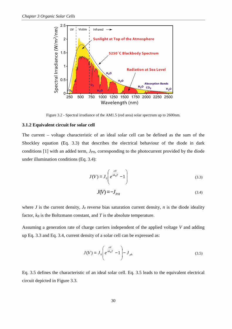
Chapter 3 Organic Solar Cells
30
Figure 3.2 - Spectral irradiance of the AM1.5 (red area) solar spectrum up to 2600nm.
3.1.2 Equivalent circuit for solar cell
The current – voltage characteristic of an ideal solar cell can be defined as the sum of the
Shockley equation (Eq. 3.3) that describes the electrical behaviour of the diode in dark
conditions [1] with an added term, JPH, corresponding to the photocurrent provided by the diode
under illumination conditions (Eq. 3.4):
where J is the current density, J0 reverse bias saturation current density, n is the diode ideality
factor, kB is the Boltzmann constant, and T is the absolute temperature.
Assuming a generation rate of charge carriers independent of the applied voltage V and adding
up Eq. 3.3 and Eq. 3.4, current density of a solar cell can be expressed as:
Eq. 3.5 defines the characteristic of an ideal solar cell. Eq. 3.5 leads to the equivalent electrical
circuit depicted in Figure 3.3.
−= 1)( 0
Tnk
eV
BeJVJ (3.3)
PHJVJ −=)( (3.4)
ph
Tnk
eV
JeJVJ B −
−= 1)( 0 (3.5)

Chapter 3 Organic Solar Cells
31
Figure 3.3 - Ideal solar cell consisting of a current source and an ideal diode in parallel.
As mentioned above, the Shockley equation (Eq. 3.5) can only be used for describing the
electrical behaviour of ideal solar cells. In real devices, additional parallel resistance (RP) and
series resistance (RS) must be taken into account.
• Parallel resistance (RP): also known as shunt resistor RSH. It is due to shunt currents
through shorts or pin-holes in the device.
• Series resistance (RS): represents Ohmic losses in the front and rear electrodes mainly
due to the contact resistances.
Considering the effects of RP and RS the equivalent electrical circuit becomes (Figure 3.4):
Figure 3.4 - Equivalent circuit of a solar cell including an additional shunt resistor RP as well as a series resistor RS.
Solving the equivalent circuit, the electrical characteristics of a non-ideal solar cell can be
described by the following equation [1–3]:
p
sph
Tnk
JRVe
R
JRVJeJVJ B
s −+−
−=
−
1)()(
0 (3.6)

Chapter 3 Organic Solar Cells
32
3.1.3 Spectral Response of solar cell
The spectral response SR (λ) is an important way to characterise the optical response of the solar
cell and, in general, is a powerful tool to optimise their performance. The spectral response
represents the current per irradiated light power in A/W for a certain wavelength. SR (λ) can be
expressed as the JPH per incident power (Eq. 3.7):
Furthermore, the External Quantum Efficiency (EQE) of a device determines the conversion
efficiency of an absorbed photon into a free charge carrier (extracted electron-hole pair) and
depends on wavelength (Eq. 3.8).
The EQE can be derived from the spectral response considering that the energy of a photon EP =
hc / λ with h being Planck’s constant, c the speed of light and q the elementary charge using the
following (Eq. 3.9):
The short-circuit current density expected under a light source can be estimated from the EQE
and the spectral irradiance of the light source by integrating the product of the EQE and the
photon flux density (Eq. 3.10):
where 5.1AMEλ is the spectral irradiance of the AM1.5 spectrum.
The EQE can be converted into the internal quantum efficiency (IQE) if only the fraction of the
actually absorbed photons is considered (Eq. 3.11):
where R(λ) is the reflected light and T(λ) is the transmitted light.
)(
)()(
λλ
λP
JSR ph= (3.7)
photonsincident of
circuit external of electrons of
N
NEQE ≡ (3.8)
λ
λλq
hcSREQE )()( = (3.9)
λλλ λ dEhc
qEQEJ AMSC
5.1
0)(∫
∞= (3.10)
)()(1
)()(
λλλλTR
EQEIQE
−−=
(3.11)

Chapter 3 Organic Solar Cells
33
3.2 Working principle of Photovoltaic Solar Cells
In this section, the physics behind the working principles of organic solar cells will be briefly
described. To understand the physics behaviour of organic solar cell requires a deep knowledge
of the working principle of a photovoltaic solar cell. We review in the following the fundamental
principles for photovoltaic effect. A general approach is introduced to describe solar cells in
terms applicable to all possible device structures including p-n homo- and heterojunction cells
(i.e., Si, CIGS, CdTe), bulk heterojunction devices (i.e., organic solar cells), or nanostructured
photoelectrochemical cells (i.e., DSCs)[4–5].
1. Any photovoltaic device requires a light absorber that converts electrons from thermal
equilibrium into an excited state upon absorption of photons (Figure 3.5). Upon photon
absorption, an electron is excited into an electronic state at higher energy, leaving a
positive charge behind at low energy.
Figure 3.5 - Ideal structure of a photovoltaic device. The currents are driven by the gradient of electrochemical potential. On the left hand side the holes are blocked, while on the right and side electrons are blocked before
reaching the contacts. Figure adapted from [6].
2. Either this excited state is metastable by itself or the electron is transferred into a
metastable, high-energy state while the remaining positive charge gets into a metastable
low-energy state.
3. A transport mechanism is necessary to bring electrons to a high electron energy contact
or (negative potential), while the remaining positive charge needs a driving force to
achieve the low energy contact [4]. Currents of electrons and holes respectively are
driven by gradients of their electrochemical potential.
4. The contacts have to show some selectivity for charge collection such that positive
charges cannot recombine with electrons from the high-energy contact, while electrons
from the high energy-state should not reach the low-energy contact.

Chapter 3 Organic Solar Cells
34
The selectivity of the contacts can be achieved using different approaches. The simple way is to
add a thin layer with a strong selectivity character (for holes or electrons). These layers are
usually called Hole (or Electron) Transport Layer (HTL, ETL). A HTL should be inserted
between the donor and the anode electrode, whereas the ETL should be placed between acceptor
and cathode electrode.
Examples of materials used as HTL in organic devices (including OLEDs and TFTs) are:
• Transition Metal Oxides (TMOs): molybdenum oxide (MoOx) [7], vanadium pentaoxide
(V2O5) [8], tungsten trioxide (WO3) [9–10], rhenium dioxide (ReO2) [11], nickel oxide
(NiO) [12].
• Solution processed organic materials: poly(3,4-ethylenedioxythiophene) polystyrene
sulfonate (PEDOT-PSS) [13], triindoles, triazatruxene (TAT), and N-trimethyltriindole
(TMTI) [14].
• Carbon-based nanostructures: Carbon nanotubes (CNT) [15] and Graphene oxide (GO)
[16–18].
As ETL the following compounds have been reported to have good selectivity for electrons:
• Lithium fluoride (LiF) [19], calcium (Ca) [20], bathocuproine (BCP) [21],
bathophenanthroline (BPhen) [22], 1,3,5-tris(2-N-phenylbenzimidazolyl) benzene (TPBi)
[23], zinc oxide (ZnO) [24], titanium oxide (TiOx) [25], caesium carbonate (Cs2CO3)
[26].
The concept of the selectivity contacts was first introduced some years ago by some authors (see
for example: Peter Würfel [5] and Juan Bisquert [27]). Although for many years this approach
was used to describe the electrical behaviour of organic and dye sensitized solar cells, its
simplicity and powerfulness it has caused that more and more authors use it as the theoretical
framework for explaining the photovoltaic working principle of other types of solar cells; as well
as crystalline silicon solar cells [28–29].
This definition is useful to describe any kind of photovoltaic solar cell, and can be easily applied
to cells with an intrinsic absorber sandwiched between an n- and p- doped layers (n-i-p or p-i-n).
Electrons are excited into some electronic state in the conduction band (CB), directly followed
by phonon emission such that electrons decay to the bottom of the CB, which is the metastable
high-energy state. The electric field across the intrinsic layer provides a driving force for electron

Chapter 3 Organic Solar Cells
35
and hole transport toward the respective contact, while a doped n- and p-type layer close to the
high- and low-energy contact provides the required transport selectivity due to a valence band
(VB) offset that creates a barrier for hole transport toward the cathode, and a anode offset
between the absorber and the p-type layers blocks electrons from recombining at the anode [30].
Organic solar cells operate very similar to p-i-n cells with the difference that the metastable high-
energy state corresponds to the LUMO level of the acceptor while the HOMO level of the donor
defines the low-energy state. Photovoltaic action in p-n homojunction silicon solar cells is often
entirely attributed to the built-in electric field that provides a driving force for holes and
electrons toward the cathode and anode, respectively. However, selective charge collection at the
cathode is at least as important to achieve high conversion efficiencies.
While the above principles are basic requirements for PV action, they do not say much about the
efficiency of the process. For the development of efficient single-junction solar cells, additional
criteria have to be fulfilled:
• The energy bandgap of the absorber (EG) should be in the range between 0.9 and 1.7 eV
(absorption onset between 1380 and 730 nm), for which the detailed balance limit
predicts a theoretical efficiency limit above 30%. This bandgap estimation take into
account that photons with sub-band-gap energy are not absorbed (hν < EG) while only a
fraction of the photon energy (EG / hν) above the band gap is converted into electric
power while the fraction (hν − EG) / hν is mostly converted into heat.
• The inverse absorption coefficient α−1 should be shorter than the minority carrier
diffusion length LD. This criteria is a rather rough statement saying that within a minority
carrier diffusion length, most of the photons should be absorbed in order to provide
diffusion as a transport mechanism to reach the respective contact. This statement is
useful for the development of new absorber materials because α−1 as well as LD are
material properties and can be characterised without the need to produce the whole
device. However, this criteria neglects additional parameters that can cause a gradient of
the minority carrier quasi-Fermi level 1 (which is the driving force minority carrier), such
as the electric fields, gradients of the electron affinity, and band gap or band
1 Quasi Fermi level is a term that describes the population of charges separately in the conduction band or valence band, when their populations are displaced from equilibrium. This displacement could be caused by the application of an external voltage, or by exposure to light.

Chapter 3 Organic Solar Cells
36
discontinuities. In contrast to the diffusion length, these parameters are defined by the
device structure and can only be characterised in a complete solar cell.
• During the transport from the absorber to the high- and low-energy contact, the loss of
energy due to discontinuities of the valence or the conduction band has to be minimised.
As the previous point, this parameter is defined by device structure, which provides a
general guideline for the band structure of a solar cell.
3.3 Working principle of Organic Solar Cells
At this point, it is worthwhile to note that, in contrast to inorganic semiconductors, the term
donor and the term acceptor are used in relation to organic solar cells. Thus, a donor can
describe a molecule (material) which transfers an electron to another molecule. Therefore, an
acceptor can describe a molecule (material) which receives an electron from another molecule.
Another important difference of organic versus inorganic semiconductors is the existence of the
exciton. The exciton is an electron-hole pair, where electron and hole are bound by Coulomb
force (Eq 3.12).
where r is the distance between the two charges q, ɛ0 is the vacuum permittivity and ɛ the
permittivity of the organic medium.
In organic semiconductors the formed excitons are Frenkel type, whereas in inorganic
semiconductors (like crystalline silicon) they usually are Wannier Mott-type. The latter are often
thermally dissociated at room temperature, which is not the case in a Frenkel exciton where the
binding energy is ten times greater. Due to the high dielectric constant the Wannier Mott exciton
has a radius larger than the lattice spacing; in contrast, Frenkel excitons tend to be small, of the
same order as the size of the unit cell because of the low dielectric constant values found in
organic semiconductors. This aspect is of essential importance to describe the operation of
organic solar cells, as discussed below.
Due to the low dielectric constant permittivity in organic materials (∼3) photoexcitation leads to
a strongly bound exciton, which needs (in the case of solar cells) to be dissociated into free
electrons and holes (carriers) [31]. The dissociation takes place at the donor/acceptor (D/A)
2
2
04
1
r
qFC πεε
= (3.12)

Chapter 3 Organic Solar Cells
37
interface. Once the exciton is dissociated, electron and hole, diffuse up to the corresponding
electrodes, where they are collected and giving rise to an electric current.
Exciton dissociation is energetically favourable when the energy of binding exciton (EEX) is
larger than the difference between ionization potential of the donor (IPD) and the electron affinity
of the acceptor (EAA) [32–33].
If the difference is not sufficient the exciton will recombine (geminate recombination) without
contributing to the photocurrent. Exciton dissociation can also occur at the organic
semiconductor/metal interfaces or in presence of impurities (e.g. oxygen) [34].
Organic solar cells are generally fabricated in thin film form of donor (D) and acceptor (A)
materials, with suitable energy levels matching, between two electrodes. One electrode must be
transparent to allow the incident light reaching the photoactive materials.
The conversion of the photon energy into free charge carriers in an organic solar cell could be
explained in the follow simplified steps (Figure 3.6):
1. Light absorption of the photon in one of the respective absorber layers (shown here for a
donor layer and exciton creation.
2. Exciton diffusion to the donor/acceptor interface.
3. Charge transfer state: exciton gets separated due to a favourable energy offset
overcoming the exciton binding energy [35–36].
4. Charge transport: free charge carriers are generated and transported through the
respective layer.
5. Collection of the charges at the electrodes.
EBexc > IPD – EAA (3.13)

Chapter 3 Organic Solar Cells
38
Light absorption
The first step in the photovoltaic process consists in the absorption of the light. In most organic
solar cell only a small percentage of the incident light is absorbed. Principal reasons are:
• Thickness of photoactive materials: the organic layer is too thin. Low charge carrier
mobilities and the low exciton diffusion lengths require layer thickness between 20 and
100 nm. Fortunately, the high optical absorption coefficients (e.g. > 105 cm−1) of organic
semiconductors allow that organic solar cells could work with a layer thickness of a few
tens of nanometres.
• Semiconductor bandgap too high with typically values about 2 eV. Besides the high
absorption coefficient, only a small portion of the incident light is absorbed because of
higher bandgap values.
When the electron is excited by the light absorption an exciton is created. For most organic
semiconductors permittivity values (ɛ) lies between 1 and 6 [37] which is quite low compared to
the permittivity of inorganic semiconductors (as for instance silicon) which exhibits ɛ = 12.
Excitons in inorganic semiconductors are usually of Wannier-Mott type. Their radius is in most
cases larger than the lattice spacing and the charges are quasi-free. In contrast, the attractive
force between electrons and holes in organic solids, where the exciton is initially localised in one
molecule, is much higher and the binding energy is comparably strong. Such strongly bound
excitons are called Frenkel excitons [38].
LUMO
LUMO
HOMO
HOMO Transparent
anode reflective
cathode
1 2
3 4
4
5
5
- -
+ + +
-
DONOR
ACCEPTOR
Figure 3.6 - Diagram showing the photogeneration in organic solar cell: from photon absorption to free carriers.

Chapter 3 Organic Solar Cells
39
Exciton diffusion
After the generation of excitons, they diffuse through the donor or acceptor phase and dissociate
into free charges at the D/A interface or recombine wasting the photons. Ideally, all photoexcited
excitons should reach the D/A interface, but due to the small exciton diffusion length some
excitons recombine before to reach the D/A interface. The exciton diffusion length (LD) can be
estimated by (Eq. 3.14):
where τ0 is the lifetime of the exciton and D is the diffusion coefficient. In literature, exciton
diffusion lengths can vary from 1 nm to more than 50 nm, depending on the material [39–41].
Due to their electrical neutrality, exciton movement is not affected by electric field, and
consequently, they diffuse through the organic semiconductor isotropically. This diffusion is
usually described as a Förster-type incoherent energy transfer process [42] and typically acts to
lower the energy of the exciton. The diffusion process can result in trapping of the exciton in
states originating from aggregates or defects. These states give rise to the tail of the density of
states [43].
Only the excitons which are able to reach the D/A interface can contribute to the photocurrent.
Exciton diffusion lengths have strong influence on the device design, because of the trade-off
between light absorption and recombination. As consequence, the active layer thickness must be
tuned to absorb light and to allow the exciton to reach the D/A interface.
Charge transfer state
At the D/A interface, strongly bound excitons might dissociate, contributing to charge carrier
generation. The dissociation of the exciton happens via an intermediate state, a so-called charge
transfer (CT) state. The electrons will be transferred to the electronegative acceptor, provided
that the exciton binding energy (EBexc) is overcome by this charge transfer process. This
requirement is often satisfied by an energetic offset between the donor and acceptor LUMOs. If
the electron is transferred from the LUMO of the donor to the LUMO of the neighbouring
acceptor the charge transfer (CT) exciton is formed, where the resulting electron-hole pairs still
experience Coulombic attraction because donor and acceptor phases are physically close to each
other at the interfaces. Then, in this intermediate state the two charges are located on separate
neighbouring molecules [44–45] (Figure 3.7). The binding energy of the CT state (EBCT) was
DLD 0τ= (3.14)

Chapter 3 Organic Solar Cells
40
reported to be in the range of 0.1–0.5 eV [46–48], which is significantly larger than the thermal
energy at room temperature (~25 meV).
Figure 3.7 - Scheme of the creation of exciton and charge-transfer states. The energy of this state depends upon the Coulomb attraction of the electron and hole and therefore their separation as illustrated by the dotted ellipsoid. For
simplicity, the binding energies are shown relative to the LUMOs.
Charge Transport
Once the charge carriers are separated, the electrons are in the acceptor phase whereas hole
remains in the donor phase. Free charges must be transported from the D/A interface through the
organic materials towards the respective electrodes to produce photocurrent. The charge
transport in organic materials can be described by a hopping mechanism [49], instead of band
transport. In the case of solar cells, the driving force is mainly the gradient of electrons and holes
concentration. Thus, the free charges (electrons and holes) diffuse to corresponding electrode.
Currents of electrons and holes are driven by gradients of their electrochemical potential. The
only possible loss mechanism in the charge transport is recombination between electrons and
holes during the journey to the electrodes (bimolecular recombination). Nevertheless, this
process is known to be very efficient and fast. A common measure for charge transport
efficiency is the mobility-lifetime (μτ) product, which expresses the average distance a charge
carrier travels at a fixed electric field before it recombines. Further analysis and experiments
have been done about μτ product in Chapter 6.
Collection the charges
An efficient collection of charges at their respective electrodes requires that the charge must
overcome the potential barrier of organic/metal interface [50]. This can be realised by using
doped layers to create selective contacts. The semipermeable contacts let the collection of one

Chapter 3 Organic Solar Cells
41
kind of charge carriers through and block the other one. There is only a direct loss path if
contacts are not selective and a charge carrier reaches the “wrong” contact, where it recombines.
External Quantum Efficiency
Each of these steps of conversion of photon energy into free charge carriers occurs with a certain
efficiency η. The EQE of organic solar cells can be expressed multiplying these efficiencies (Eq.
3.15):
where ηA is related to the photon absorption efficiency, ηED to the exciton diffusion efficiency,
ηCT to the charge transfer efficiency, and ηCC to the carrier collection efficiency. The ηED restricts
the EQE, because of the exciton diffusion length has values in the range of nanometres. The
distance an exciton is able to travel during its lifetime has strong influence on the design and
optimisation of materials and devices (i.e. the thicknesses of active layers).
From the spectra of the EQE, photocurrent contribution of a limited wavelength region can be
studied. Hence, the contribution of each material to the photocurrent can be obtained, since the
different photoactive materials absorb in different spectral regions.
3.3.1 Carrier Recombination
Recombination processes are mechanisms losses that decrease the power conversion efficiency
of the solar cells. There are two types of recombination in organic solar cells: geminate and
nongeminate recombination.
• Geminate recombination takes place when a coulombically bound electron–hole pair
(exciton) generated from the absorption of a single photon recombines before the electron
and hole are separated into free charge carriers. The probability of geminate
recombination is independent of carrier density and geminate losses happen within
nanoseconds of absorption [51–52].
• Nongeminate recombination is the recombination of free charge carriers and
encompasses both trap-assisted (Shockley-Read-Hall) and bimolecular mechanisms
(Langevin). Nongeminate recombination losses are carrier density dependent and
typically occur after micro to milliseconds when illumination conditions are comparable
1 sun [53–54].
EQE = ηA ηED ηCT ηCC (3.15)

Chapter 3 Organic Solar Cells
42
Geminate recombination
Onsager was the first to described quantitatively geminate recombination [55]. His model
calculates the probability that a coulombically bound electron-hole pair will escape its Coulomb
attraction and generate free charges. The competition between dissociation of CT state and its
recombination to the ground state depends upon the magnitude of the coulombic attraction felt
by this CT state (Figure 3.8). In particular, Onsager proposed a definition for a Coulomb capture
radius (alternatively called the Onsager radius), rc, define the distance at which the Coulomb
attraction energy equals the thermal energy kBT. If the thermalisation length a is greater than the
Coulomb capture radius rc, the charge carriers are considered to be fully dissociated. If, however,
the thermalisation length is smaller than rc, then the dissociation of the CT state into free charges
occurs with a certain escape probability, while geminate recombination occurs with a
complementary probability.
Figure 3.8 - Electron thermalisation length (a) versus coulomb capture radius (rC).
Nongeminate recombination
Direct nongeminate recombination refers to the recombination of a free electron with a free hole
in the semiconductor. Most often, nongeminate recombination takes place via defect states in the
gap (Shokley-Read-Hall), where a free electron (or hole) is captured by a trapped hole (or
electron). Nongeminate recombination is usually referred in the literature as bimolecular
recombination, in the sense that the electron and hole that recombina come from different
dissociated excitons.

Chapter 3 Organic Solar Cells
43
3.3.2 Parameters characteristics of Organic Solar Cells
In the next paragraphs the VOC, JSC, parasitic resistances (RP, RS) and FF will be analysed in
detail for the case of organic solar cells.
Open Circuit Voltage
The VOC is related to the splitting of the quasi-Fermi levels of hole and electron in the active
layer under steady-state illumination at the anode and cathode (Figure 3.9) [56]. Under this
condition, carrier generation and recombination exactly balance each other and no net current
exists at any point inside the device.
Figure 3.9 - The open circuit voltage in organic solar cells is related to the difference between HOMO level of the
donor and LUMO level of the acceptor.
Many reports have shown that in organic solar cells, VOC is linearly correlated to the difference
between the HOMO level of the donor and the LUMO level of the acceptor (Eq. 16) [57–58],
and it does not depend on the work functions of the electrodes [59].
where q is the elementary charge, EHOMO,D is the HOMO level energy of the donor and ELUMO,A
is the LUMO level energy of the acceptor. One the most cited work was done by Brabec et al. in
2001 [57]. They synthesized a series of fullerene derivatives with different LUMO levels and
blended them with a common donor poly(2-methoxy-5-(30,70-dimethyloctyloxy)- 1,4-
phenylenevinylene) (MDMO-PPV). In their experiments, VOC was always linearly dependent on
the LUMO level of the acceptor. While the work function of the cathode varied in the wide range
of 2.87 eV (Ca) to 4.28 eV (Au), the variation of VOC was comparatively very small (<0.2 V). In
2006, Scharber [58] carefully studied a series of organic solar cell devices (26 polymer donor
VOC = (1/q) (|EHOMO,D| –|ELUMO,A| – ∆) (3.16)

Chapter 3 Organic Solar Cells
44
materials with different HOMO levels blended with a common acceptor), and proposed an
empirical value of 0.3 for VOC losses. It should be noted that the VOC loss of 0.3 eV is obtained
from experimental data, and it is not based on theoretical background. A similar relation was
reported by Veldman et al. [60] based on a detailed analysis of the charge transfer emission in
polymer/fullerene blends. A number of studies suggested that the physical reasons of this 0.3V
loss factor limiting the maximum achievable VOC in organic solar cells could be related to the
effect of disorder [61–62]. Durrant and co-workers [63–64] analyse the impact of charge carrier
recombination and the donor acceptor microstructure on the VOC of bulk polymer solar cells.
They developed a comprehensive model describing the VOC of bulk heterojunction solar cells
device based on transient optoelectronic analyses. They found for different polymer-fullerene
solar cells VOC losses in the range of 0.225–0.435V.
Although the origin of the losses has been discussed widely no clean conclusions have been
established. Anyhow, there is a consensus the major losses resulting in a decreased VOC are
related to the disorder in organic semiconductors [65] and non-geminate recombination [66].
Materials for organic solar cells are soft materials. During the film preparation, interactions
between molecules, kinks in the polymer chains, and the degrees of crystallinity of organic
semiconductors can all introduce disorder into the system. Furthermore, the regioregularity,
molecular weight, and purity variation are all important causes of disorder. The control of film
deposition is an important subject in the field of organic solar cells. Thus, disorder should also be
taken into consideration when discussing origin of VOC in organic solar cell.
As consequence of disorder and defects localised states appear within the bandgap of the
semiconductor. Similar to the well-studied inorganic hydrogenated amorphous silicon (a-Si:H)
semiconductor, disorder induces band tails states and deep traps in the electronic structure. The
distribution in the gap states downshifts the electron quasi-Fermi level and upshifts the hole
quasi-Fermi level, which obviously reduces VOC. For the same reason, disorder in organic
materials plays a role in bringing the electron quasi-Fermi level down away from the LUMO
level of the acceptor, and lifting up the hole quasi-Fermi level away from the HOMO level of the
donor, and consequently reduce the VOC. The distribution of density of states (DOS) in the tail
can be approximated as a Gaussian or exponential type.
Nongeminate recombination in organic solar cells annihilates carriers and hence causes energy
loss, reducing VOC as a result. At VOC photo-generated carriers remain and accumulate inside the
device, thereby bimolecular mechanism governs the recombination.

Chapter 3 Organic Solar Cells
45
The influence of the DOS on the VOC in small-molecule organic solar cells is discussed in section
3 of Chapter 5.
Short Circuit Current
The JSC in organic solar cell is ideally proportional to the absorbed photons and dependent on the
free charges carriers to reach the electrodes. The number of photons absorbed depends on the
absorption coefficient of the material and the device architecture, as well as the thickness of the
active layer or reflecting back electrodes [1].
The major loss of JSC is leaded by monomolecular recombination, where carriers recombine
through a trap or a recombination centre.
Parasitic Resistances
• Parallel resistance (Rp): In organic solar cells, Rp is mainly attributed to recombination
of charge carriers near the donor-acceptor interface.
• Series resistance (Rs): In organic solar cells, Rs considers conductivity i.e. mobility of
the specific charge carrier in the respective transport medium. For example, mobility of
holes in a p-type material. The mobility can be affected by space charges and traps. Rs is
also increased with a longer travelling distance of the charges in i.e. thicker transport
layers.
Fill Factor
The value of FF depends mainly on parasitic resistances. Typical values for FF are 0.65 to 0.85
for good organic solar cells.
3.4 Device architecture
In the following a brief summary, including the strengths and weak points, of the four most used
architectures of organic solar cells is given:
Single layer cell. Single layer structures consist of only one semiconductor material between two
electrodes (Figure 3.10). Single layer cells and are often referred to as Schottky type devices or
Schottky diodes since charge separation occurs at the rectifying (Schottky) junction with one
electrode. The other electrode interface is supposed to be of ohmic contact [67–70]. The

Chapter 3 Organic Solar Cells
46
structure is simple but the absorption is usually low using a single type of molecule. Since both
positive and negative charges travel through the same material, recombination losses are
generally high.
Figure 3.10 - Diagram of single layer organic solar cell.
Bilayer cell. This kind of solar cell contain two layers sandwiched with the conductive electrodes
(Figure 3.11).This structure benefits from the separated charge transport layers that ensure
connectivity with the correct electrode and give the separated charge carriers only little chance to
recombine with its counterpart. The principal drawback is the small interface area that allows
only excitons to reach it and get dissociated.
This architecture has an important limitation which relates to the exciton diffusion length in the
organic materials. The exciton diffusion length is dependent on the exciton lifetime and is in the
range of 10–40 nm.
Figure 3.11 - Diagram of bilayer organic solar cell.
Bulk Heterojunction cell. A mixture of donor and acceptor materials is sandwiched between
anode and cathode (Figure 3.12). The strong point of this type is the large interface area,
allowing high molecular mixing and, thereforen, most excitons can reach the D/A interface. This
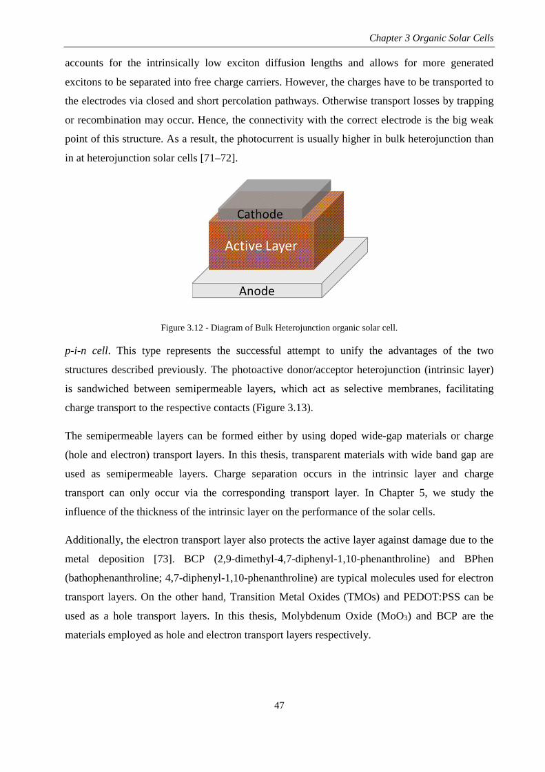
Chapter 3 Organic Solar Cells
47
accounts for the intrinsically low exciton diffusion lengths and allows for more generated
excitons to be separated into free charge carriers. However, the charges have to be transported to
the electrodes via closed and short percolation pathways. Otherwise transport losses by trapping
or recombination may occur. Hence, the connectivity with the correct electrode is the big weak
point of this structure. As a result, the photocurrent is usually higher in bulk heterojunction than
in at heterojunction solar cells [71–72].
Figure 3.12 - Diagram of Bulk Heterojunction organic solar cell.
p-i-n cell. This type represents the successful attempt to unify the advantages of the two
structures described previously. The photoactive donor/acceptor heterojunction (intrinsic layer)
is sandwiched between semipermeable layers, which act as selective membranes, facilitating
charge transport to the respective contacts (Figure 3.13).
The semipermeable layers can be formed either by using doped wide-gap materials or charge
(hole and electron) transport layers. In this thesis, transparent materials with wide band gap are
used as semipermeable layers. Charge separation occurs in the intrinsic layer and charge
transport can only occur via the corresponding transport layer. In Chapter 5, we study the
influence of the thickness of the intrinsic layer on the performance of the solar cells.
Additionally, the electron transport layer also protects the active layer against damage due to the
metal deposition [73]. BCP (2,9-dimethyl-4,7-diphenyl-1,10-phenanthroline) and BPhen
(bathophenanthroline; 4,7-diphenyl-1,10-phenanthroline) are typical molecules used for electron
transport layers. On the other hand, Transition Metal Oxides (TMOs) and PEDOT:PSS can be
used as a hole transport layers. In this thesis, Molybdenum Oxide (MoO3) and BCP are the
materials employed as hole and electron transport layers respectively.

Chapter 3 Organic Solar Cells
48
Figure 3.13 - Diagram of p-i-n organic solar cell
Tandem Cells. Organic tandem solar cells were first introduced by Hiramoto et al. in 1990 [74].
Tandem solar cells with organic semiconductors are solar cells with multiple D/A
heterojunctions made of different semiconductor materials. Ideally, each D/A heterojunction will
produce electric current in response to different wavelengths of light; thereby a broader
harvesting of the solar spectrum is achieved [75]. Thermal evaporation processing allows an easy
stacking of organic layers to form multiple heterojunctions.
The tandem solar cells concept is particularly interesting in the case of small-molecule solar cells
with p-i-n structure. The single p-i-n devices feature good device performance with high FF and
high Internal Quantum Efficiency (IQE). Nevertheless, to achieve high power conversion
efficiencies both IQE and the total absorption need to be high. The single p-i-n cells suffer from
too low absorption in two aspects. Firstly, the absorption spectra of the photoactive layers do not
cover the complete range of the sun spectrum. In addition, the photoactive layers have to be thin
enough to avoid recombination losses and space charge limitation of the current flow. Therefore,
they are optically thin even at the absorption maxima.
An approach to overcome these problems is to stack several junctions with either identical or
complementary absorption spectra on top of each other. The VOC is then given by the sum of the
open circuit voltages of the individual cells. The flow of photocurrent in stacked junction cells
requires easy recombination of charge carriers with low energetic losses at the interface between
the individual cells. For that reason, each D/A heterojunction is separated by a thin layer as
recombination zone, shown in Figure 3.14 [76].
Today, this architecture combined with p-i-n subcells has achieved the world record efficiency in
organic solar cells.

Chapter 3 Organic Solar Cells
49
Figure 3.14 - Diagram of tandem organic solar cell.

Chapter 3 Organic Solar Cells
50
References
[1] H. Hoppe, N. S. Sariciftci, “Organic solar cells: an overview”, J. Mater. Res. 19, (2004) 1924.
[2] N. W. Ashcroft, N. D. Mermin, “Solid state physics”, Saunders College Publishing, Fort Worth, 1976.
[3] A. W. Hains, Z. Liang, M. A. Woodhouse, B. A. Gregg, “Molecular semiconductors in organic photovoltaic cells”, Chem. Rev. 110 (2010) 6689.
[4] M. A. Green, “Photovoltaic Principles”, Physica E 14 (2002) 11.
[5] P. Würfel, “Physics of Solar Cells – From Principles to New Concepts”, Wiley-VCH: New York, 2005.
[6] S. Rühleet, A. Y. Anderson, H-N. Barad, B. Kupfer, Y. Bouhadana, E. Rosh-Hodesh, A. Zaban, “All-Oxide Photovoltaics”, J. Phys. Chem. Lett. 3 (2012) 3755.
[7] D. W. Zhao, P. Liu, X. W. Sun, S. T. Tan, L. Ke, A. K. K. Kyaw, “An inverted organic solar cell with an ultrathin Ca electron-transporting layer and MoO3 hole-transporting layer”, Appl. Phys. Lett. 95 (2009) 153304.
[8] J Meyer, K Zilberberg, T Riedl, A Kahn, “Electronic structure of Vanadium pentoxide: An efficient hole injector for organic electronic materials”, J. Appl. Phys. 110 (2011) 033710.
[9] S. Han, W. S. Shin, M. Seo, D. Gupta, S. J. Moon, S. Yoo, “Improving performance of organic solar cells using amorphous tungsten oxides as an interfacial buffer layer on transparent anodes”, Org. Electron. 10 (2009) 791
[10] C. Tao, S. Ruan, G. Xie, X. Kong, L. Shen, F. Meng, C. Liu, X. Zhang, W. Dong, W. Chen, “Role of tungsten oxide in inverted polymer solar cells” Appl. Phys. Lett. 94 (2009) 043311.
[11] Z. Tan, L. Li, F. Wang, Q. Xu, S. Li, G. Sun, X. Tu, X. Hou, J. Hou, Y. Li, “Solution-Processed Rhenium Oxide: A Versatile Anode Buffer Layer for High Performance Polymer Solar Cells with Enhanced Light Harvest”, Adv. Energy Mater. 4 (2014) 1300884.
[12] M. D. Irwin, D. B. Buchholz, A. W. Hains, R. P. H. Chang, T. J. Marks, “p-Type semiconducting nickel oxide as an efficiency-enhancing anode interfacial layer in polymer bulk-heterojunction solar cells” Proc. Natl. Acad. Sci. USA 105 (2007) 2783.
[13] J. Ouyang, C.-W. Chu, F.-C. Chen, Q. Xu, Y. Yang, “High-Conductivity Poly(3,4-ethylenedioxythiophene):Poly(styrene sulfonate) Film and Its Application in Polymer Optoelectronic Devices”, Adv. Funct. Mater. 15 (2005) 203.
[14] S. W. Shelton, T. L. Chen, D. E. Barclay, B. Ma, “Solution-Processable Triindoles as Hole Selective Materials in Organic Solar Cells”, ACS Appl. Mater. Interfaces 4 (2012) 2534.
[15] E. Kymakis, M. M. Stylianakis, G. D. Spyropoulos, E. Stratakis, E. Koudoumas, C. Fotakis, “Spin coated carbon nanotubes as the hole transport layer in organic photovoltaics” Sol. Energ. Mat. Sol. Cells 96 (2012) 298.

Chapter 3 Organic Solar Cells
51
[16] S. -S. Li, K. -H. Tu, C. -C. Lin, C. -W. Chen, M. Chhowalla, “Solution-Processable Graphene Oxide as an Efficient Hole Transport Layer in Polymer Solar Cells”, ACS Nano 4 (2010) 3169.
[17] J.-M. Yun, J.-S. Yeo, J. Kim, H.-G. Jeong, D.-Y. Kim, Y.-J. Noh, S.-S. Kim, B.-C. Ku, S.-I. Na, “Solution-Processable Reduced Graphene Oxide as a Novel Alternative to PEDOT: PSS Hole Transport Layers for Highly Efficient and Stable Polymer Solar Cells”, Adv. Mater. 23 (2011) 4923.
[18] F. Bonaccorso, Z. Sun, T. Hasan, A. C. Ferrari, “Graphene photonics and optoelectronics”, Nature Photon. 4 (2010) 611.
[19] K. Kawano, C. Adachi, “Reduced initial degradation of bulk heterojunction organic solar cells by incorporation of stacked fullerene and lithium fluoride interlayers”, Appl. Phys. Lett. 96 (2010) 053307.
[20] B. Paci, A. Generosi, V. Rossi Albertini, P. Perfetti, R. de Bettignies, C. Sentein, “Time-resolved morphological study of organic thin film solar cells based on calcium/aluminium cathode material”, Chem. Phys. Lett. 461 (2008) 77.
[21] J. Huang, J. Yu, H. Lin, Y. Jiang, “Detailed analysis of bathocuproine layer for organic solar cells based on copper phthalocyanine and C60” J. Appl. Phys. 105 (2009) 073105.
[22] N -N. Wang, J. -S. Yu, H. Lin, Y. -D. Jiang “Organic Photovoltaic Cells with Improved Performance Using Bathophenanthroline as a Buffer Layer” Chin. J. Chem. Phys. 23 (2010) 84.
[23] J. Yu, N. Wang, Y. Zang, Y. Jiang, “Organic photovoltaic cells based on TPBi as a cathode buffer layer”, Sol. Energ. Mat. Sol. Cells 95 (2011) 664.
[24] Y. Sun, J. H. Seo, C. J. Takacs, J. Seifter, A. J. Heeger, “Inverted Polymer Solar Cells Integrated with a Low-Temperature-Annealed Sol-Gel-Derived ZnO Film as an Electron Transport Layer” Adv. Mater. 23 (2011) 1679.
[25] C. Waldauf, M. Morana, P. Denk, P. Schilinsky, K. Coakley, S. A. Choulis, C. J. Brabec, “Highly efficient inverted organic photovoltaics using solution based titanium oxide as electron selective contact”, Appl. Phys. Lett. 89 (2006) 233517.
[26] F. C. Chen, J. L. Wu, S. S. Yang, K. H. Hsieh, W. C. Chen, “Cesium carbonate as a functional interlayer for polymer photovoltaic devices” J. Appl. Phys.103 (2008) 103721.
[27] J. Bisquert, “Nanostructured Energy Devices: Equilibrium Concepts and Kinetics” CRC Press, 2014.
[28] A. Cuevas, D. Yan, “Misconceptions and misnomers in solar cells”, IEEE J. Photovoltaics, 3 (2013) 916.
[29] U. Würfel, A. Cuevas, P. Würfel, “Charge Carrier Separation in Solar Cells”, IEEE J. Photovoltaics 5 (2015) 461.
[30] W. Jaegermann, A. Klein, T. Mayer, “Interface Engineering of Inorganic Thin-Film Solar Cells - Materials-Science Challenges for Advanced Physical Concepts. Adv. Mater. 21 (2009) 4196.

Chapter 3 Organic Solar Cells
52
[31] G. P. Nicholson, A. F. Castro, “Organic photovoltaics: principles and techniques for nanometre scale characterization”, Nanotechnology 21 (2010) 492001.
[32] N. S. Sariciftci, L. Smilowitz, A. J. Heeger, F. Wudl, “Semiconducting polymers (as donors) and buckminsterfullerene (as acceptor): photoinduced electron transfer and heterojunction devices”, Synt. Met. 59 (1993) 333.
[33] J. J. M. Halls, J. Cornil, D. A. dos Santos, R. Sibley, D. H. Wang, A. B. Holmes, J. L. Bredas, R. H. Friend, “Charge-and energy-transfer processes at polymer/polymer interfaces: A joint experimental and theoretical study” Phys. Rev. B 60 (1999) 5721.
[34] J.-M. Nunzi, “Organic photovoltaic materials and devices”, C. R. Physique 3 (2002) 523.
[35] J. J. M. Halls, K. Pichler, R.H. Friend, S.C. Moratti, A.B. Holmes, “Exciton diffusion and dissociation in a poly(p-phenylenevinylene)/C60 heterojunction photovoltaic cell”, Appl. Phys. Lett. 68 (1996) 3120.
[36] J.J.M. Halls, R. H. Friend, “The photovoltaic effect in a poly(p-phenylenevinylene)/perylene heterojunction”, Synth. Met. 85 (1997) 1307.
[37] O. D. Gordan, M. Friedrich, D. R. T. Zahn, “The anisotropic dielectric function for copper phthalocyanine thin films”, Org. Electron. 5 (2004) 291.
[38] J. Frenkel, “Some remarks on the theory of the photoelectric effect”, Phys. Rev. 38 (1931) 309.
[39] S. Yoo, B. Domercq, B. Kippelen, “Efficient thin-film organic solar cells based on pentacene/C60 heterojunctions”, Appl. Phys. Lett. 85 (2004) 5427.
[40] D. E. Markov, E. Amsterdam, P. W. M. Blom, A. B. Sieval, J. C. Hummelen, “Accurate measurement of the exciton diffusion length in a conjugated polymer using a heterostructure with a side-chain cross-linked fullerene layer”, J. Phys. Chem. A 109 (2005) 5266.
[41] Y. Terao, H. Sasabe, C. Adachi, “Correlation of hole mobility, exciton diffusion length, and solar cell characteristics in phthalocyanine/fullerene organic solar cells”, Appl. Phys. Lett. 90 (2007) 103515.
[42] T. Förster, “Energiewanderung und Fluoreszenz”, Naturwissenschaften 33 (1946) 66.
[43] P. Peumans, A. Yakimov, S. R. Forrest, “Small molecular weight organic thin-film photodetectors and solar cells” J. Appl. Phys. 93 (2003) 3693.
[44] A. Petersen, A. Ojala, T. Kirchartz, T. A. Wagner, F. Wurthner, U. Rau, “Field-dependent exciton dissociation in organic heterojunction solar cells” Phys. Rev. B 85 (2012) 245208.
[45] B. A. Gregg, J. van de Lagemaat, “Solar cells: Folding photons” Nature Photon. 6 (2012) 278.
[46] X.-Y. Zhu, Q. Yang, M. Muntwiler, “Charge-transfer excitons at organic semiconductor surfaces and interfaces”, Acc. Chem. Res. 42 (2009) 1779.
[47] T. Drori, C.-X. Sheng, A. Ndobe, S. Singh, J. Holt, Z. V. Vardeny, “Below-gap excitation of π-conjugated polymer-fullerene blends: Implications for bulk organic heterojunction solar cells”, Phys. Rev. Lett. 101 (2008) 037401.

Chapter 3 Organic Solar Cells
53
[48] M. Hallermann, S. Haneder, E. Da Como, “Charge-transfer states in conjugated polymer/fullerene blends: Below-gap weakly bound excitons for polymer photovoltaics”, Appl. Phys. Lett. 93 (2008) 053307.
[49] H. Bässler, “Charge Transport in Disordered Organic Photoconductors a Monte Carlo Simulation Study”, Phys. Stat. Sol. (b) 175 (1993) 15.
[50] L- M. Chen, Z. Xu, Z. Hong, Y. Yang, “Interface investigation and engineering – achieving high performance polymer photovoltaic devices”, J. Mater. Chem. 20 (2010) 2575.
[51] D. Credgington, F. C. Jamieson, B. Walker, T. -Q. Nguyen, J. R. Durran, “Quantification of geminate and non-geminate recombination losses of a solution-processed diketopyrrolopyrrole-based bulk heterojunction solar cell”, Adv. Mater. 24 (2012) 2135.
[52] J. Kniepert, M. Schubert, J. C. Blakesley, D. Neher, “Photogeneration and recombination in P3HT/PCBM solar cells probed by time-delayed collection field experiments”, J. Phys. Chem. Lett. 2 (2011) 700.
[53] C. G. Shuttle, B. O’Regan, A. M. Ballantyne, J. Nelson, D. D. C. Bradley, J. R. Durrant, “Bimolecular recombination losses in polythiophene:fullerene solar cells” Phys. Rev. B 78 (2008) 113201.
[54] S. R. Cowan, W. L. Leong, N. Banerji, G. Dennler, A. J. Hegger, “Identifying a threshold impurity level for organic solar cells: enhanced first-order recombination via well-defined PC84BM traps in organic bulk heterojunction solar cells”, Adv. Funct. Mater. 21 (2011) 3083.
[55] L. Onsager, “Initial Recombination of Ions”, Phys. Rev., 54 (1938) 554.
[56] J. Bisquert, D. Cahen, G. Hodes, S. Rühle, A. Zaban, “Physical chemical principles of photovoltaic conversion with nanoparticulate, mesoporous dye-sensitized solar cells”, J. Phys. Chem. B 108 (2004) 8106.
[57] C. J. Brabec, A. Cravino, D. Meissner, N. S. Sariciftci, T. Fromherz, M. T. Rispens, L. Sanchez, J. C. Hummelen, “Origin of the open circuit voltage of plastic solar cells”, Adv. Funct. Mater. 11 (2001) 374.
[58] M. C. Scharber, D. Mühlbacher, M. Koppe, P. Denk, C. Waldauf, A. J. Heeger, C. J. Brabec, “Design rules for donors in bulk-heterojunction solar cells-towards 10% energy-conversion efficiency”, Adv. Mater. 18 (2006) 789.
[59] C. Uhrich, D. Wynands, S. Olthof, M. K. Riede, K. Leo, S. Sonntag, B. Maennig, M. Pfeiffer, “Origin of open circuit voltage in planar and bulk heterojunction organic thin-film photovoltaics depending on doped transport layers”, J. Appl. Phys. 104 (2008) 043107.
[60] A. Veldman, S.C.J. Meskers, R.A.J. Janssen, “The energy of charge-transfer states in electron donor-acceptor blends: insight into the energy losses in organic solar cells” Adv. Funct. Mater. 19 (2009)1939.
[61] P.K. Nayak, G. Garcia-Belmonte, A. Kahn, J. Bisquert, D. Cahen, “Photovoltaic efficiency limits and material disorder”, Energy Environ. Sci. 5 (2012) 6022.

Chapter 3 Organic Solar Cells
54
[62] A. Manor, E.A. Katz, “Open-circuit voltage of organic photovoltaics: Implications of the generalized Einstein relation for disordered semiconductors”, Sol. Energ. Mat. Sol. Cells 97 (2012) 132.
[63] D. Credgington, J. R. Durrant, “Insights from Transient Optoelectronic Analyses on the Open-Circuit Voltage of Organic Solar Cells” J Phys. Chem. Lett. 3 (2012) 1465.
[64] C. G. Shuttle, B. O’Regan, A. M. Ballantyne, J. Nelson, D. D. C. Bradley, J. de Mello, J. R. Durrant, “Experimental determination of the rate law for charge carrier decay in a polythiophene:fullerene solar cell” Appl. Phys. Lett. 92 (2008) 1.
[65] G. García-Belmonte, J. Bisquert, “Open-circuit voltage limit caused by recombination through tail states in bulk heterojunction polymer-fullerene solar cells” Appl. Phys. Lett. 96 (2010) 113301.
[66] D. Credgington, R. Hamilton, P. Atienzar, J. Nelson, J. R. Durrant, “Non-Geminate Recombination as the Primary Determinant of Open-Circuit Voltage in Polythiophene:Fullerene Blend Solar Cells: an Analysis of the Influence of Device Processing Conditions” Adv. Funct. Mater. 21 (2011) 2744.
[67] C. W. Tang, A. C. Albrecht, “Photovoltaic effects of metal–chlorophyll-a–metal sandwich cells”, J. Chem. Phys. 62 (1975) 2139.
[68] Y. Y. Merritt, H. J. Hovel, “Organic solar cells of hydroxy squarylium”, Appl. Phys. Lett. 29 (1976) 414.
[69] F. J. Karnpas, M. Gouterman, “Merocyanine organic solar cells”, J. Phys. Chem. 81 (1977) 690.
[70] D. L. Morel. A. K. Ghosh. T. Feng. E. L. Stogryn. P. E. Purwin, R. F. Shaw, C. Fishman, “High-efficiency organic solar cells”, Appl. Phys. Lett. 32 (1978) 495.
[71] A. W. Hains, Z. Liang, M. A. Woodhouse, B. A. Gregg, “Molecular semiconductors in organic photovoltaic cells”, Chem. Rev. 110 (2010) 6689.
[72] F. Padinger, R. Rittberger, N. Sariciftci, “Effects of Postproduction Treatment on Plastic Solar Cells”, Adv. Funct. Mater. 13 (2003) 85.
[73] P. Peumans, A. Yakimov, S. Forrest, “Small molecular weight organic thin-film photodetectors and solar cells”, J. Appl. Phys. 93 (2003) 3693.
[74] M. Hiramoto, M. Suezaki, M. Yokoyama, “Effect of thin gold interstitial-layer on the photovoltaic properties of tandem organic solar cell”, Chem. Lett. 19 (1990) 327.
[75] M. Riede, C. Uhrich, J. Widmer, R. Timmreck, D. Wynands, G. Schwartz, W.-M. Gnehr, D. Hildebrandt, A. Weiss, J. Hwang, S. Sundarraj, P. Erk, M. Pfeiffer, K. Leo, “Efficient organic tandem solar cells based on small molecules”, Adv. Funct. Mater. 21 (2011) 3019.
[76] J. Xue, B. Rand, S. Uchida, S. Forrest, “A hybrid planar-mixed molecular heterojunction photovoltaic cell”, Adv. Mater. 17 (2005) 66.

55
4. Materials and Experimental Methods This Chapter presents the materials used in this thesis to fabricate the solar cells. Additionally,
the thin film deposition techniques and the experimental set-up used for solar cell deposition and
characterisation are explained in detail.
4.1 Materials
The chemical structure and the main optoelectronic properties of the organic semiconductors
used in this work are presented in this section.
Tetraphenyldibenzoperiflanthene
Tetraphenyldibenzoperiflanthene (DBP) is a p-type semiconductor (donor electron material).
DBP molecule has a symmetrical structure (Figure 4.1). DBP molecule is only composed of
carbon and hydrogen atoms.
Figure 4.1 - Structure of Tetraphenyldibenzoperiflanthene (DBP)
Numerous donor materials have been developed in last decades. DBP is a promising electron
donor material for photovoltaic applications and has been used in many laboratories around the
world since 2009 [1–6].
The principal advantages of DBP in application to solar cells are the high optical absorption and
the high HOMO level. High optical absorption values allow a reduction in the thickness of the
active layer, which is a favourable condition for the exciton to reach the donor – acceptor (D/A)
interface. The HOMO energy level of DBP is estimated to be around -5.5eV [1], which makes

Chapter 4 Materials and Experimental Methods
56
DBP suitable for employment with fullerene acceptors. The high HOMO energy leads to a high
open circuit voltage (VOC) because the difference between the HOMO energy of the donor and
the lowest unoccupied molecular orbital (LUMO) energy of the acceptor is proportional to VOC
[7].
Fullerene C70
A fullerene is any molecule composed of only carbon atoms in the form of a hollow sphere,
ellipsoid, tube, and many other shapes. C70 is the fullerene molecule consisting of 70 carbon
atoms. It is a cage-like structure which resembles a rugby ball, made of 25 hexagons and 12
pentagons, with a carbon atom at the vertices of each polygon and a bond along each polygon
edge (Figure 4.2).
Figure 4.2 - Structure of fullerene C70
C70 was discovered in 1985 by Robert Curl, Harold Kroto and Richard Smalley [8]. They found
Cn clusters (for even n with n > 20) using laser evaporation of graphite of which the most
common were C60 and C70. They were awarded the 1996 Nobel Prize in Chemistry for their
discovery of fullerenes.
C70 is used as electron acceptor and electron transporting molecule. The energy levels of C70 are
-6.1eV for the IP and -4.0eV for EA. C70 can forms brownish crystals with a bandgap of 1.77 eV
[9].
Molybdenum oxide MoO3
Molybdenum oxide is a transition metal oxide (TMO). Previous works presented transition metal
oxides such as V2O5, WO3, and MoO3 as conducting p-type materials, with the electron affinity
and ionization energy of MoO3 in the order of 2.3 and 5.3–5.4 eV, respectively [10–11].
However, it has been recently demonstrated with direct and inverse photoemission spectroscopy
measurements that MoO3 exhibits a high electron affinity (EA) of 6.7 eV and may consequently
be used as p-type dopant for materials with deep HOMO levels. MoO3 as well as other similar
transition metal oxides are n-type materials exhibiting very deep lying electronic states and more

Chapter 4 Materials and Experimental Methods
57
commonly used as hole transport layer [12–15]. In Figure 4.3, a schematic energy-level diagram
of several TMOs and organic semiconductors. The lower shaded regions represent the valence
bands and the upper shaded regions represent the conduction bands. The dashed lines indicate
the position of the Fermi level for each oxide. Oxides with their Fermi levels close to the valence
band are p-type semiconductors, and oxides with their Fermi levels close to the conduction band
are n-type semiconductors [16].
Figure 4.3 - Schematic energy-level diagrams of (a) several transition metal oxides and (b) several organic
semiconductors. Figure obtained from [16].
MoO3 is one of the most commonly used transition metal oxide in organic electronics
applications, because it is evaporated at relatively low temperature (~ 400 °C). Hence, it can be
easily deposited in vacuum from a crucible. In contrast, the evaporation temperatures of V2O5
and WO3 are significantly higher.
MoO3 layer has been used in OLEDs to improve hole injection from the anode to the organic
emitters. Moreover, it has been reported that devices containing MoO3 are more stable in the air
than those fabricated using alternative hole transport layer (like PEDOT:PSS) [17]. Metal oxides
interlayer has also been used in organic photovoltaic cells. Enhancement in power conversion
efficiencies was observed. In particular, the use of MoO3 interlayer between the ITO anode and
the donor layer in small-molecule solar cells enhance the fill factor due to the reduction in series
resistance, which improves the power conversion efficiency [14].

Chapter 4 Materials and Experimental Methods
58
Bathocuproine BCP
Bathocuproine, 2,9-dimethy-4,7-diphenyl -1,10-phenathroline (Figure 4.4), also called BCP, is a
well known material used as electron transport layer in applications such as organic light-
emitting diodes [18] and organic solar cells [19–21]. The appearance of BCP is white or yellow
crystalline powder. BCP is soluble in organic solvents such as nitrobenzene and insoluble in
water.
Figure 4.4 - Chemical structure of bathocuproine (BCP).
BCP is a wide-gap electron transport material. The role of BCP layer inserted between active
layer and aluminium contact in organic solar cells was investigated by Vogel et al. [20]. In that
work, BCP dramatically improves electron transport out of the C60 film into the aluminium
electrode. Consequently, BCP buffer layer reduces geminate recombination of excitons at the
C60–Al interface. For that reason, the BCP layer is used to make a selective cathode. In addition,
it prevents damage to the active organic layer by the metal deposition. The optimal BCP
thickness for application in organic solar cells is between 8 and 10 nm [21].
4.2 Experimental Methods
The fabrication process of organic solar cells is detailed in this section. Substrate preparation,
organic and metal depositions are described. At the end of the chapter, specifications of electrical
set up used for devices characterisation are exposed.
The fabrication and characterisation of the devices of this thesis has been carried out the Centre
for Research in Nanoengineering (CRnE) and in the clean room facilities of the Departament
d’Enginyeria Electrònica (DEE) from Universitat Politècnica de Catalunya. MNT group has a
long experience on the fabrication of solar cells based on inorganic semiconductors (silicon).
Clean room facilities (located in the basement of the DEE, Campus Nord) used for fabrication
and characterisation of solar cells are detailed below.

Chapter 4 Materials and Experimental Methods
59
Facilities at the Clean Room of the DEE
There are several deposition systems in the clean room of UPC: one evaporation system based on
electron beam and Joule effect, another evaporation system based on magnetron sputtering and a
Plasma Enhanced Chemical Vapour Deposition (PECVD) system devoted to the deposition of
hydrogenated amorphous silicon and alloys. In addition, thermal ovens are utilised to perform
annealing, doping diffusion processes and to growth silicon dioxide on crystalline silicon wafers.
Moreover, two photolithographic systems with resolution around one micrometre are used. In
order to measure the film thickness there are a profilometer and an ellipsometer. The last is used
to measure the thickness and index of refraction for thin dielectric films.
At the moment, MNT the research activities based on inorganic solar cells include: crystalline
silicon solar cells with interdigitated back contact electrodes (maximum efficiency 22%),
Heterojunction with Intrinsic Thin-Film (HIT solar cells, with 18% efficiency). Besides, MNT
group is also fabricating porous silicon for thermo-photovoltaic applications.
As it mentioned in the Chapter 1, the MNT group from DEE proposed to fabricate organic solar
cells about ten years ago. In 2002, the MNT group started a new research line focused on the
fabrication of organic devices based on small-molecules semiconductors. The objective was to
widen up the technology know-how of the group. For this purpose, the group acquired a new
deposition systems based on two Joule-effect evaporators (Oerlikon). The MNT group acquired
the organic evaporator UNIVEX 300 from Leybold Systems (Figure 4.5). The group began the
research in organic electronics with manufacturing organic field effect transistors (OFETs) to
study the electronic properties of organic semiconductors. Metal contacts were deposited using
the evaporator from Edwards. The need to avoid oxygen incorporation during the device
fabrication pushed the group to be equipped with a new evaporation system integrated in a
glovebox.
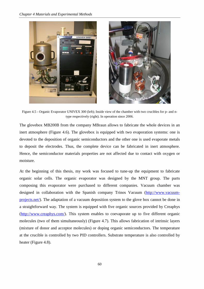
Chapter 4 Materials and Experimental Methods
60
Figure 4.5 - Organic Evaporator UNIVEX 300 (left); Inside view of the chamber with two crucibles for p- and n-
type respectively (right). In operation since 2006.
The glovebox MB200B from the company MBraun allows to fabricate the whole devices in an
inert atmosphere (Figure 4.6). The glovebox is equipped with two evaporation systems: one is
devoted to the deposition of organic semiconductors and the other one is used evaporate metals
to deposit the electrodes. Thus, the complete device can be fabricated in inert atmosphere.
Hence, the semiconductor materials properties are not affected due to contact with oxygen or
moisture.
At the beginning of this thesis, my work was focused to tune-up the equipment to fabricate
organic solar cells. The organic evaporator was designed by the MNT group. The parts
composing this evaporator were purchased to different companies. Vacuum chamber was
designed in collaboration with the Spanish company Trinos Vacuum (http://www.vacuum-
projects.net/). The adaptation of a vacuum deposition system to the glove box cannot be done in
a straightforward way. The system is equipped with five organic sources provided by Creaphys
(http://www.creaphys.com/). This system enables to coevaporate up to five different organic
molecules (two of them simultaneously) (Figure 4.7). This allows fabrication of intrinsic layers
(mixture of donor and acceptor molecules) or doping organic semiconductors. The temperature
at the crucible is controlled by two PID controllers. Substrate temperature is also controlled by
heater (Figure 4.8).

Chapter 4 Materials and Experimental Methods
61
Figure 4.6 - Glovebox MB200B from MBraun with metal evaporator in 2010, before the installation of organic
evaporator.
Figure 4.7 - Top view of organic evaporation sources. Each organic source is equipped with a shutter (controlled
externally). Moreover an additional shutter is located behind the holder substrate.
Acceptors
Dopants
Donors

Chapter 4 Materials and Experimental Methods
62
Figure 4.8 - Schematic of organic chamber with the connections between the three temperature controllers with five
evaporation sources and substrate holder.
The metal evaporator uses Joule-effect to evaporate thin films onto a given substrate. It can
deposit materials with a specified thickness of up to 1500 nanometers. Deposition rate is
controlled by the use of a quartz crystal monitor. It was programmed to evaporate with a suitable
rate in order to not damage the organic layers. Finally, the glovebox was ready to fabricate
organic solar cells in 2012 (Figure 4.9).
Figure 4.9 - Glovebox MB200B from MBraun with our home-made organic evaporator in 2012.
In the following paragraphs, the facilities distributed between CRnE and DEE used for the
characterisation of films and devices are exposed.

Chapter 4 Materials and Experimental Methods
63
CRnE facilities
Purification System
High material purity is one critical aspect to the functioning of organic electronic devices. It is
possible to aim for purities > 99.9%, typically even >> 99.99% independently of the initial purity
of the raw material. A purification organic semiconductor leads to higher power efficiency and
longer lifetime of the devices. The optimised process can get a material yield of about 20%. The
Tube-based Vacuum Sublimation System (CreaPhys GmbH) provides the means to purify
organic volatile compounds by gradient thermal sublimation in vacuum. The DSU-05 has a
nominal capacity of 5 g, which are, however, strongly dependent on the material properties like
density, sublimation and melting behaviour. The system features a three zone gradient oven.
Figure 4.10 shows the result of sublimation CuPc. Initially, the aim of DSU-05 system was to
purify organic compounds provided by chemist laboratories specialized in synthesis.
Nevertheless, the system has not been used very often due to the low yielding.
Figure 4.10 - Purification of CuPc molecules.
Focused Ion Beam
The Zeiss Neon 40 combines the imaging and analytical capabilities of a high resolution
Scanning Electron Microscope (SEM) with a Focused Ion Beam (FIB) column (Figure 4.11). In
addition, this cross-beam system has a multi-channel gas injection system (GIS) for deposition of
metal and insulating layers, and can also perform enhanced and selective etching. This cross-
beam workstation is used for sample observation, selective milling and deposition, 3D

Chapter 4 Materials and Experimental Methods
64
tomography, Transmission Electron Microscopy (TEM) lamella preparation, microfabrication
and elemental analysis.
Figure 4.11 - Cross-beam workstation Zeiss Neon 40
Atomic Force Microscope
In this thesis, the Atomic Force Microscopy (AFM) has been used to measure the topography of
the organic thin-films in tapping mode. In fact, the basic technique of AFM, which is contact
AFM, is not well adapted to examine such surfaces due to problems of friction and adhesion.
Therefore, the tapping mode of operation was developed to overcome drawbacks of contact
mode [22]. This mode uses oscillation of the cantilever tip at or near its natural resonant
frequency while allowing the cantilever tip to impact the target sample for a minimal amount of
time. This intermittent contact lessens the damage done to the soft surface and to the tip,
compared to the amount done in contact. Hence the dragging forces during scanning are greatly
reduced [23]. Moreover, during oscillation, the tip goes through both the attractive and the
repulsive regions of the tip-sample force field.
The Dimension 3100 Nanoman AFM from Veeco (Figure 4.12) provides a variety of high
resolution surface imaging techniques, such as: atomic force microscopy, in tapping and contact
mode or Kelvin probe or surface potential microscopy (KPM) among others.

Chapter 4 Materials and Experimental Methods
65
Figure 4.12 - Atomic Force Microscope Dimension 3100 Nanoman from Veeco
Spectrophotometer
This equipment allows complete characterisation of the optical properties of thin-film layers; in
particular allows the measure of optical density. UV-visible-NIR Spectrophotometer (Shimadzu
3600) has UV-probe software for photometric analysis of solid and liquid materials in the 185 to
3300 nm range (Figure 4.13). It is equipped with ISR 3100 integrating sphere and transmission
liquid sample holder.
Figure 4.13 - UV-visible-NIR Spectrometer. Shimadzu 3600.
Profilometer
Thicknesses of thin film layers were determined ex-situ by Veeco DEKTAK 150 profilometer
(Figure 4.14). The profilometer measures the vertical depth of a material across a specified
horizontal length. The profile is displayed on a graphical interface. Uses for this equipment
include measuring etch depth, deposited film thickness, and surface roughness. The resolution of
a step to determine the film thickness is about tens of nanometres.

Chapter 4 Materials and Experimental Methods
66
Figure 4.14 - Veeco DEKTAK 150 (right) with DEKTAT Stylus (left)
4.2.1 Fabrication process for Organic Solar Cells
Organic solar cells fabricated in MNT-UPC are processed by thermal evaporation in high
vacuum conditions, which is the most generally used method for depositing low weight organic
compounds [24]. The use of this technique has some advantages over solution – processable thin
films in the application of organic optoelectronic devices. Higher control of the structure and
morphology of the films is possible because solvents are not required, leading to a high
reproducibility of device fabrication. The flexibility in device design (i.e. layer thicknesses,
multilayer structure, materials selection) is an intrinsic attribute of dry processing techniques
such as thermal evaporation. In this work, the structure of the fabricated organic solar cells
consist of a glass substrate with a transparent electrode acting as the anode, the organic films and
the top metal contact acting as the cathode.
Vacuum deposition Systems
Vacuum deposition is a family of processes used to deposit layers of material atom-by-atom or
molecule-by-molecule on a solid surface. The deposited layers can range from a thickness of one
atom up to millimetres. When the vapour source is a liquid or solid the process is called physical
vapour deposition (PVD), on the other hand if the source is a chemical vapour precursor the
process is called chemical vapour deposition (CVD). The vacuum environment in thermal
evaporation reduce the particle density, hence the mean free path for collision is long and
reducing the particle density of undesirable molecules or atoms (contaminants).
Three types of flow are mostly encountered in vacuum technology: viscous or continuous flow,
molecular flow and Knudsen flow at the transition between these two. A backing pump, working
in viscous flow, is needed in a high vacuum system to start turbomolecular pump, since
turbomolecular pumps usually work in the pressure region below 10-3 mbar. In this thesis, the

Chapter 4 Materials and Experimental Methods
67
high vacuum systems used to evacuate the evaporator chambers are comprised by a
turbomolecular pump and an oil-sealed rotary pump.
Thermal evaporation process consists on the sublimation of a compound from a resistively
heated crucible or boat (source) in vacuum from 10−6 mbar to 10−10 mbar onto a substrate [25].
Hence, a molecular beam is created from the boat to the substrate. This molecular beam is
defined by the elongated shape of the boat. The mean free path of the molecules evaporated in
the vacuum chamber is usually longer than the size of the chamber. Consequently, the molecules
can travel from the source to the substrate without collide with other molecules in the chamber.
The limitation in the deposition rate is fixed by the escape rate of the molecules from the solid or
melt phase into vacuum, since molecular transport through vacuum is almost immediate. The
deposition rate is controlled by the source temperature. Using shutters for substrate and sources,
which can interrupt the molecular beam, allow nanometre control of film thickness.
The quartz crystal microbalance (QCM) coating thickness gauge (thin film controller) utilizes
the piezoelectric sensitivity of a quartz oscillator (monitor crystal) to measure the supplied mass
on the gauge. This property is utilised to monitor the deposition rate and film thickness during
vacuum coating. A very sharp electromechanical resonance occurs at different discrete
frequencies of the voltage applied. Resonance frequency is reduced when a quantity of mass is
added to the surface of the quartz crystal oscillating in resonance. This frequency shift is very
reproducible.
Fabrication process
Preparation of the substrates is very important in order to obtain reproducible results. All the
solar cells presented in this thesis are fabricated on glass coated with the transparent conductor
indium tin oxide (In2O3:SnO2, ITO) (Luminescence Technology Corporation). Glass substrates
with pre-patterned ITO have a sheet resistance of 12Ω/sq and a thickness of 120 nm (Figure
4.15).

Chapter 4 Materials and Experimental Methods
68
The ITO surface is cleaned in an ultrasonic bath with acetone (15 min) and isopropyl alcohol (15
min) and dried with nitrogen flux. Finally, the substrates are treated in ultraviolet/ozone for 30
min. This treatment increases the work function [26] and removes any remaining carbon
residues.
Once substrates are cleaned, they are transferred into the vacuum system for film deposition.
Organic layers were deposited by thermal evaporation under a base pressure of approximately
10-7 mbar at a rate in the range of 0.1–0.2 Å/s. The substrate temperature is a crucial parameter
for the morphology of the film. For that reason, substrate temperature was controlled during the
organic deposition molecules. In Chapter 5, a detailed work about the influence of the deposition
substrate temperature on the optoelectronic properties of the donor material is presented.
The crucible or boat, holding the evaporation material, is at the core of the evaporation process.
A conical alumina (Al2O3) boat is used in this work (Figure 4.16). The alumina boat can achieve
high temperatures, above 500ºC. The maximum temperature reached in this thesis was 350ºC, to
evaporate fullerene C70.
Glove box MBraun200B has integrated the vacuum deposition system MB-EcoVap which
allows evaporating metals (Figure 4.17). The equipment includes several recipes programmable
1,5cm
1,5cm
0,4cm 0,4cm 0,7cm
ITO
Figure 4.15 - Geometry of ITO patterned substrate.
Figure 4.16 - Alumina boat (left). Alumina boat inside the heater system equipped with shutter (right).

Chapter 4 Materials and Experimental Methods
69
PLC control to evaporate different metals. There are two evaporation sources controlled
independently. This double source setup allows the evaporation and co-evaporation of different
metal layers without break the vacuum with nitrogen. A structure to hold the mask with 9 solar
cells substrates were designed and adapted in MB-EcoVap system. Moreover, there is an
automatic mechanism with electro-pneumatic valves to lift the chamber.
Figure 4.17 - MB-EcoVap (left); inside view with holder for mask (right).
The metal used as the cathode in the organic solar cells was aluminium. Aluminium was
presented in form of pellet. The metal was deposited by thermal evaporation on organic layers
through metallic shadow mask to give an active are of 0.075 cm2 (Figure 4.18). Deposit rate was
below than 0.2 Å/s during first 20nm and 1 Å/s up to required thickness. Since the evaporated
material reaches the substrate mostly from a single direction, during the evaporation process the
samples rotated at 30 rpm to obtain a uniform layer.
Figure 4.18 - Shadow metal mask for evaporation (left); substrate with four organic solar cells, its active area is
0.075 cm2 (right).

Chapter 4 Materials and Experimental Methods
70
Metal deposition is an extremely critical point in organic small-molecules solar cells. Metal
atoms may diffuse though organic layers; this effect can short the device.
Figure 4.19 shows a typical SEM image of the cross-section of an organic solar cell based on
CuPc and C60. In this case, the structure of the solar cell was glass/ITO/CuPc/C60/Ag. The cross-
section was obtained by using a FIB process. The observed layer thicknesses are in agreement
with profilometry measurements. In addition, the layers are uniform and no shortcircuits are
visible.
Figure 4.19 - Cross-section of organic solar cell.
4.2.2 Characterisation of Organic Solar Cells
Electrical characterisations of all devices were carried out in nitrogen ambient using a plastic
prototype (Figure 4.20), specifically designed to minimise oxygen and humidity degradation.
This prototype allows the measurement of 4 different substrates with 4 cells in each substrate in
nitrogen atmosphere. Metallic tips contact all anodes and cathodes of solar cells. There are two
selectors that allow selecting one solar cell from a specific substrate. The prototype has been
fabricated by the company microLIQUID.

Chapter 4 Materials and Experimental Methods
71
Figure 4.20 - Prototype to measure organic solar cells in nitrogen atmosphere.
Current – Voltage Measurement
The most important characterisation is the measurement of the current-voltage characteristics (I-
V curve), delivering the power conversion efficiency. The basic parameters of I-V characteristics
are discussed in Chapter 3. Devices were measured at room temperature in the dark and under
AM 1.5G conditions using a solar simulator (Newport Oriel Instruments Model: 94061A Class
ABB (Figure 4.21).
Figure 4.21 - Solar simulator Newport Oriel Model 94061A Class ABB.
Illumination source uses a Xenon lamp and a proprietary filter to meet Class A performance
parameters without compromising the one sun output power in 6 x 6 inch area (Figure 4.22). The
overall illumination intensity is calibrated with a pyranometer prior to each measurement run.

Chapter 4 Materials and Experimental Methods
72
Figure 4.22 - Spectral output of Solar Simulator with standard AM1.5G filter (Newport).
The measurements were carried out applying bias and recording the current using a HP 4142B
DC Source measurement unit. A Matlab interface was used to control the source meter and
record the I-V curves.
External Quantum Efficiency Measurement
The External Quantum Efficiency (EQE) of a solar cell is given by the extracted electron hole
pairs per incident photons. EQE measurements of photovoltaic cells were performed with a
quantum efficiency integrated system, model QEX10 (PV Measurements, Inc.), under standard
measurement conditions using a 150 W xenon lamp coupled with a slit monochromator (Figure
4.23). The intensity of incident monochromatic light was calibrated with a Si photodiode. The
QEX10 spectral response system uses an adjustable mechanical chopper to modulate the light at
rates between 4 Hz and 200 Hz, chopping frequency was fixed at 66 Hz to avoid any
perturbation from light ambient. The measurements were carried out in the wavelength range of
300 nm to 800 nm at resolution of 5 nm.
Figure 4.23 - Quantum efficiency integrated system, model QEX10 (PV Measurements, Inc.).

Chapter 4 Materials and Experimental Methods
73
Variable Intensity Measurement
The solar cell performance is dependent on light intensity. Measuring the J–V curve over a wide
range of illumination levels, rather than at a fixed illumination level of 100 mW/cm2, can be
obtained additional information about the device performance. We call this method the Variable
Illumination Measurement (VIM) method. From the J–V measurements at different illumination
levels, a model of an organic solar cell can be obtained. In this thesis, a study about the
recombination of organic solar cells is detailed in Chapter 6.
The VIM measurements were carried out in Departament de Física Aplicada i Òptica of the
Universitat de Barcelona (UB) (Figure 4.24). The illumination level can vary from 10 mW/cm2
(0.1 suns) to 200 mW/cm2 (2 suns) by means of neutral grey filters to preserve the spectral
distribution of the incident light (Figure 4.25).
Figure 4.24 - Image of characterisation setup for Variable Intensity Measurements.
PC Conditioning electronics
Light source
Filter No. 1 Filter No. 2
Fiber optic
PV device
Figure 4.25 - Scheme of Variable Intensity Measurement.

Chapter 4 Materials and Experimental Methods
74
References
[1] D. Fujishima, H. Kanno, T. Kinoshita, E. Maruyama, M. Tanaka, M. Shirakawa, K. Shibata, “Organic thin-film solar cell employing a novel electron-donor material”, Sol. Energy Mater. Sol. Cells, 93 (2009) 1029.
[2] M. Hirade, C. Adachi, “Small molecular organic photovoltaic cells with exciton blocking layer at anode interface for improved device performance”, Appl. Phys. Lett. 99 (2011) 153302.
[3] D. Yokoyama, Z. Qiang Wang, Y.-J. Pu, K. Kobayashi, J. Kido, Z. Hong, “High-efficiency simple planar heterojunction organic thin-film photovoltaics with horizontally oriented amorphous donors”. Sol. Energy Mater. Sol. Cells 98 (2012) 472.
[4] Y. Zheng, W. J. Potscavage, T. Komino, M. Hirade, J. Adachi, C. Adachi, “Highly efficient bulk heterojunction photovoltaic cells based on C70 and tetraphenyldibenzoperiflanthene”, Appl. Phys. Lett. 102 (2013) 143304.
[5] X. Xiao, J. D. Zimmerman, B. E. Lassiter, K. J. Bergemann, S. R. Forrest, “A hybrid planar-mixed tetraphenyldibenzoperiflanthene/C70 photovoltaic cell”, Appl. Phys. Lett. 102 (2013) 073302.
[6] Z. Wang, D. Yokoyama, X. Wang, “Highly efficient organic p-i-n photovoltaic cells based on tetraphenyldibenzoperiflanthene and fullerene C70”, Energy Environ. Sci. 6 (2013) 249.
[7] B. Rand, D. Burk, S. Forrest, “Offset energies at organic semiconductor heterojunctions and their influence on the open-circuit voltage of thin-film solar cells”, Phys. Rev. B 75 (2007) 115327.
[8] H.W. Kroto, J. R. Heath, S. C. O'Brien, R. F. Curl, R. E. Smalley, “C60: buckminsterfullerene”, Nature 318 (1985) 162.
[9] K. Thirunavukkuarasu, V. C. Long, J. L. Musfeldt, F. Borondics, G. Klupp, K. Kamarás, C. A. Kuntscher, “Rotational dynamics in C70: temperature- and pressure-dependent infrared studies". J. Phys. Chem. C 115 (2011) 3646.
[10] H. You , Y. F. Dai , Z. Q. Zhang , D. G. Ma, “Improved performances of organic light-emitting diodes with metal oxide as anode buffer” J. Appl. Phys. 101 (2007) 026105.
[11] C. W. Chu, S. H. Li, C. W. Chen, V. Shrotriya, Y. Yang, “High-performance organic thin-film transistors with metal oxide/metal bilayer electrode”, Appl. Phys. Lett. 87 (2005) 193508.
[12] M. Kröger, Sami Hamwi, Jens Meyer, T. Riedl, W. Kowalsky, A. Kahn, “P-type doping of organic wide band gap materials by transition metal oxides: A case-study on Molybdenum trioxide”, Org. Electron. 10 (2009) 932.
[13] J. Meyer, K. Zilberberg, T. Riedl, A. Kahn, “Electronic structure of Vanadium pentoxide: An efficient hole injector for organic electronic materials”, J. Appl. Phys., 110 (2011) 033710.
[14] D. Y. Kim, J. Subbiah, G. Sarasqueta, F. So, H. Ding, Irfan, Y. Gao, “The effect of molybdenum oxide interlayer on organic photovoltaic cells”, Appl. Phys. Lett., 95 (2009) 093304.

Chapter 4 Materials and Experimental Methods
75
[15] M. T. Greiner, M. G. Helander, W.-M. Tang, Z.-B. Wang, J. Qiu, Z.-H. Lu, “Universal energy-level alignment of molecules on metal oxides”, Nat. Mater., 11 (2012) 76.
[16] M. T Greiner, Z-H. Lu, “Thin-film metal oxides in organic semiconductor devices: their electronic structures, work functions and interfaces”, NPG Asia Mater. 5 (2013) e55.
[17] F. Wang, X. Qiao, T. Xiong, D. Ma, “The role of molybdenum oxide as anode interfacial modification in the improvement of efficiency and stability in organic light-emitting diodes”, Org. Electron. 9 (2008) 985.
[18] Y. Masumoto, T. Mori, “Application of organic bathocuproine-based alloy film to organic light-emitting diodes”, Thin Solid Films 516 (2008) 3350.
[19] P. Peumans, S. Uchida, S. R. Forrest, “Efficient bulk heterojunction photovoltaic cells using small-molecular-weight organic thin films”, Nature 425 (2003) 158.
[20] M. Vogel, S. Doka, Ch. Breyer, M. Ch. Lux-Steiner, K. Fostiropoulos, “On the function of a bathocuproine buffer layer in organic photovoltaic cells”, Appl. Phys. Lett. 89 (2006) 163501.
[21] J. Huang, J. Yu, H. Lin, Y. Jiang, “Detailed analysis of bathocuproine layer for organic solar cells based on copper phthalocyanine and C60”, J. Appl. Phys. 105 (2009) 073105.
[22] G. Binnig, C.F. Quate, C. Gerber, “Atomic Force Microscope”, Phys. Rev. Lett. 56 (1986) 930.
[23] J. Tamayo, R. Garcia, “Deformation, contact time, and phase-contrast in tapping mode scanning force microscopy”, Langmuir, 2 (1996) 4430.
[24] S.R. Forrest, “Ultrathin organic films grown by organic molecular beam deposition and related techniques”, Chem. Rev. 97 (1997) 1793.
[25] M. Knudsen, “The law of the molecular flow and viscosity of gases moving through tubes”, Ann. Phys 28 (1909) 75.
[26] J. Xue, S. R. Forrest, “Carrier transport in multilayer organic photodetectors: II. Effects of anode preparation”, J. Appl. Phys. 95 (2004) 1869.

Chapter 4 Materials and Experimental Methods
76

77
5. Organic Solar Cells based on DBP and fullerene C70
The main results obtained on the characterisation of organic solar cells based on small-
molecules tetraphenyldibenzoperiflanthene (DBP) and fullerene C70 are presented and discussed
in this chapter.
In the first section, the electrical performance of bilayer solar cells is analysed. In particular we
will focus on the influence of the deposition substrate temperature of the donor material on the
performance of the solar cells.
In the second section, the influence of the density of localised states in the band gap of the donor
layer on the open circuit voltage (VOC) of the solar cells will be discussed.
Finally, using the optimised deposition parameters solar cells with p-i-n structure will be
fabricated, where the intrinsic layer is obtained by the coevaporation of donor and acceptor. The
influence of the thickness of the intrinsic layer of p-i-n solar cell will be studied.
5.1 Bilayer Solar Cells based on DBP and C70
5.1.1 Introduction
Solar cells based on bilayer structure (donor/acceptor) were presented in Chapter 3, section 3.3.
This structure allows higher control of the film morphology of the donor and the acceptor
material during the deposition process. As we also mentioned, the optimum geometry for high
efficiency organic solar cells would be the p-i-n structure, where the intrinsic layer is composed
of donor and acceptor material (bulk heterojunction approach). Contrary to the situation of
solution processed bulk heterojunction solar cells, this approach is not easy to optimise when
cells are based on thermal evaporated small-molecule. The coevaporation of two compounds in a
controlled manner is not easy. Since the sublimation temperatures usually are different for each
compound, the deposition rates should be stabilized separately, making the fabrication of the
solar cell a complex process. Moreover, deposition rates depend on the amount of material

Chapter 5 Organic Solar Cells based on DBP and fullerene C70
78
present in the crucible, adding more uncertainty on the control de deposition rates when both
compounds are sublimated simultaneously.
For all these reasons, our approach started with the optimisation of the optoelectronic properties
of a solar cell with bilayer structure. The fabrication of organic solar cells involves the
optimisation of different layers, each of them with very low thickness (tens of nm). In the case of
a multilayer structure composed of individual single compounds allows us to optimise separately
each of the layers of the solar cell having a good control of the thicknesses (usually in the range
of tens nanometres) of each layer. Moreover, this approach allows us to be more confident with
the measured experimental data and extract conclusive conclusions.
Our experimental deposition set-up allows the deposition of thin-film layers with good thickness
control over an area of around diameter of 5 inches (variation of 5% between the maximum
(central part) and minimum thickness (external part)). Considering this, our holder 10 cm x 10
cm allows to deposit simultaneously over 9 substrates (1 cm x 1 cm). As mentioned before
(Chapter 4) each substrate allocates 4 solar cells. This allows us to fabricate 36 organic solar
cells in a single run process. The reproducibility of the optoelectronic performance of the
fabricated solar cells is not very high, including solar cells measured on the same substrate.
Therefore, obtaining conclusive results is based on the trend observed on the evolution of the
solar cell performance with its structure/geometry and the deposition parameters used when
processing.
The basic structure of our solar cell consists on a bilayer structure of the donor and acceptor
materials sandwiched between a Hole Transport Layer (HTL) in contact with the anode electrode
and an Electron Transport Layer (ETL) in contact with the cathode electrode. In our case, we
have used molybdenum trioxide (MoO3) as HTL and BCP as ETL. The structure of the solar
cells studied in this Chapter is glass/ITO/MoO3/DBP(10nm)/C70(40nm)/BCP(8nm)/Al(150nm).
Glass substrates with prepatterned ITO were supplied by Luminiscence Technology Corporation
(Lumtec Taiwan). ITO thickness was 1200~1600Å, with a sheet resistance of 9~15 Ω/sq and a
maximum of optical transmission of 84% at 550nm. The DBP, C70, MoO3 and BCP compounds
were purchased from Sigma Aldrich. The absorbing part of the solar cell is formed by DBP
acting as a donor and C70 as an acceptor.
The substrate temperature is one of the deposition parameters that have strong influence on the
performance of thin-film solar cells. Previous works have reported the influence of substrate
temperature on the morphology of amorphous silicon thin films and its influence on the

Chapter 5 Organic Solar Cells based on DBP and fullerene C70
79
optoelectronic properties [1–3]. In this section, we study the variation in performance of bilayer
organic solar cells where the donor material was deposited at different substrate temperatures.
Fullerenes and its derivatives are the most common used electron acceptor materials to fabricate
organic solar cells due to its excellent electronic properties. Although different electron acceptor
materials have been used in solar cell technology, like perylene derivatives, its performance was
clearly lower when compared with fullerenes derivatives. Main advantages of fullerene
derivatives are its deep-lying LUMO energy level (~3.8–4.2 eV) for effective charge separation
at D/A interface and its high electron mobility.
Contrary, there are a vast number of electron donor materials. Among them, DBP has recently
emerged as a promising donor material for photovoltaic applications [4–9]. The most important
advantages of DBP in application to solar cells are its high optical light absorption and its deep
HOMO level position. High optical absorption values allow a reduction in the thickness of the
layer, which is a favourable condition for the exciton to reach the donor – acceptor (D/A)
interface. The HOMO energy level of DBP is estimated to be 5.5eV [4], which makes it
appropriate to combine with fullerene acceptors. The relatively deep HOMO level of DBP can
help to obtain a high VOC. It has been reported that VOC is related to the difference between the
HOMO level of the donor and the LUMO level of the acceptor [10].
3nm 10nm 40nm 8nm
BCP Al
5.5
3.5 3.5
6.1
4.0 4.2
8.5
5.4
5.0
ITO
6.5
MoO3 DBP C70
Figure 5.1 - Energy levels (eV) of the different layers comprising the bilayer solar cell.

Chapter 5 Organic Solar Cells based on DBP and fullerene C70
80
The electrical properties of MoO3 have been presented in Chapter 4. This material is an n-type
semiconductor exhibiting very deep lying electronic states [11–14]. Recent investigations have
led to a reinterpretation of the electronic structure of MoO3/semiconductor interfaces. The hole
injection mechanism is considered via electron extraction from the HOMO through the MoO3
conduction band [15].
5.1.2 Electrical Characterisation
The photovoltaic performances of bilayer solar cells where the DBP was deposited at different
substrate temperatures are presented in this section. First, the main photovoltaic parameters from
J–V characteristic are exposed. Following, spectral analyses of bilayer solar cells are discussed.
0,0 0,2 0,4 0,6 0,8 1,0-6
-5
-4
-3
-2
-1
0
DBP Substrate temperature
Cu
rre
nt
De
nsi
ty (
mA
/cm
2)
Voltage (V)
30
60
90
120
Figure 5.2 - Current – Voltage measurements of bilayer cells under one sun illumination with DBP layer deposited
at different temperatures.

Chapter 5 Organic Solar Cells based on DBP and fullerene C70
81
The J–V characteristics of bilayer solar cells are shown in Figure 5.2. From J–V characteristics
have been estimated the main photovoltaic parameters as a function of the DBP deposition
temperature. Results are summarised in Figure 5.3. The device with a DBP layer deposited at a
substrate temperature of 30 ºC showed a JSC = 5.29 mA/cm2, VOC = 0.79 V and FF = 46% for a
PCE = 1.9%. The best VOC and FF values were obtained for a substrate temperature of 60 ºC
during DBP deposition, leading to a maximum PCE of 2.5%. Particularly, this device achieved a
VOC = 0.89 V, FF = 58% and only the JSC = 4.79 mA/cm2 was slightly reduced with respect to
the reference device fabricated at 30 ºC. Substrate temperatures higher than 60 ºC resulted in
lower solar cell performance, basically due to the reduction of JSC.
-4,40
-4,80
-5,20
-5,60
30 60 90 120
0,80
0,84
0,88
0,92
0,45
0,50
0,55
0,60
30 60 90 120
1,75
2,00
2,25
2,50
DBP Substate Temperature (oC)
Jsc
(mA
/cm
2)
Vo
c (V
)
FF
PC
E (
%)
Figure 5.3 - Photovoltaic parameters of organic solar cells versus DBP substrate temperature.
The Optical Density (OD) of the photoactive materials DBP and C70 single layers and in a bilayer
structure are shown in Figure 5.4. Thicknesses of the DBP and C70 were 10 nm and 40 nm
respectively. The donor DBP presents different absorption bands in the visible region around

Chapter 5 Organic Solar Cells based on DBP and fullerene C70
82
330, 550 and 600 nm. The acceptor C70 shows a strong absorption band at 350 nm and a broader
band in the region of 450 nm. The OD of the DBP/C70 bilayer structure is significant from 300
nm to 700 nm. The higher OD of the device with DBP deposited at 30 ºC agrees with the highest
JSC value obtained for this device. As the deposition temperature increases, the actual thickness
of the DBP layers could be slightly reduced because of a lower sticking coefficient of the organic
molecule on the substrate. This effect could explain the reduction in the OD at higher substrate
temperatures and the decrease of the JSC values observed in Figure 5.3.
300 400 500 600 700 8000,0
0,2
0,4
0,6
0,8 30oC
60oC
90oC
120oC
DBP
C70
Op
tica
l D
en
sity
Wavelength (nm)
DBP Substrate temperature
Figure 5.4 - Optical density of the active layers used for the fabrication of bilayer solar cells.
The spectral dependence of photocurrent generation and collection was analysed by measuring
the EQE curves (Figure 5.5). The EQE curves were quite similar for all the solar cells with a
slight reduction on devices incorporating DBP deposited at higher temperatures. This behaviour
reproduces the trend observed in the measurements of the OD (Figure 5.4). The EQE curves also
evidence a good correlation with the JSC values measured for these devices.

Chapter 5 Organic Solar Cells based on DBP and fullerene C70
83
300 400 500 600 700 8000
10
20
30
40
Ext
ern
al
Qu
an
tum
Eff
icie
ncy
(%
)
Wavelength (nm)
30oC
60oC
90oC
120oC
DBPSubstrate temperature
Figure 5.5 - EQE of bilayer solar cells in which the DBP layer was deposited at different substrate temperature.
5.1.3 Morphology analysis
The effect of the substrate temperature on the topography of the DBP films was studied by
Atomic Force Microscopy (AFM). For that purpose, a series of DBP films with a thickness of 20
nm were deposited on crystalline silicon substrates. Figure 5.6 shows the top view AFM images
(1 x 1 μm2 scanning square) for four samples deposited at the different substrate temperatures. It
can be observed that pillar-like grain structures were created as the substrate temperature
increase. The density and size of these pillars also seem to increase with the substrate
temperature during the deposition of the DBP.
Figure 5.6 - AFM images of DBP thin films deposited at different substrate temperatures:
a) 30 ºC b) 60 ºC c) 90 ºC d) 120 ºC

Chapter 5 Organic Solar Cells based on DBP and fullerene C70
84
The roughness values were estimated by using software techniques and its dependence with
substrate temperature is shown in Figure 5.7. The surface of the films prepared at 30 ºC and 60
ºC was relatively smooth with roughness values around 0.35 nm. A sharp increase of the surface
roughness is observed for the films deposited at 90 ºC and 120 ºC. This modification of the
surface morphology with substrate temperature is rather similar to that reported by other groups
(Zhou et al. [16]).
30 60 90 1200,3
0,4
0,5
0,6
0,7
RM
S R
ou
gh
ne
ss (
nm
)
DBP Substrate Temperature (oC)
Figure 5.7 - Root-mean-square roughness of DBP thin films as function of the substrate temperature.
The nanostructure of the 20nm DBP layers on SiO2 substrates were also analysed by X-Ray
Diffraction (XRD) spectroscopy. The absence of diffraction peaks indicates the amorphous
nature of the samples (Figure 5.8). Therefore, we could expect that transport properties, and
particularly carrier mobility, are rather isotropic in these films.
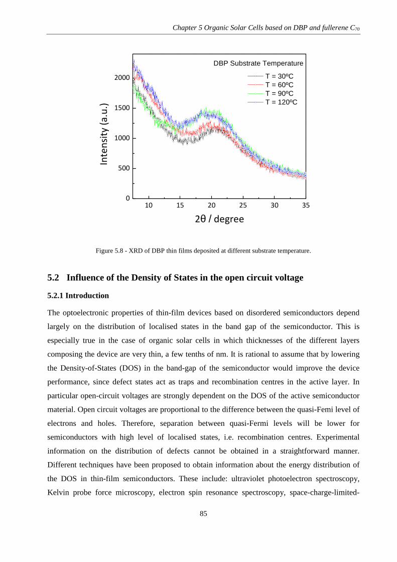
Chapter 5 Organic Solar Cells based on DBP and fullerene C70
85
10 15 20 25 30 350
500
1000
1500
2000
DBP Substrate Temperature
Inte
nsi
ty (
a.u
.)
2θ / degree
T = 30ºC T = 60ºC T = 90ºC T = 120ºC
Figure 5.8 - XRD of DBP thin films deposited at different substrate temperature.
5.2 Influence of the Density of States in the open circuit voltage
5.2.1 Introduction
The optoelectronic properties of thin-film devices based on disordered semiconductors depend
largely on the distribution of localised states in the band gap of the semiconductor. This is
especially true in the case of organic solar cells in which thicknesses of the different layers
composing the device are very thin, a few tenths of nm. It is rational to assume that by lowering
the Density-of-States (DOS) in the band-gap of the semiconductor would improve the device
performance, since defect states act as traps and recombination centres in the active layer. In
particular open-circuit voltages are strongly dependent on the DOS of the active semiconductor
material. Open circuit voltages are proportional to the difference between the quasi-Femi level of
electrons and holes. Therefore, separation between quasi-Fermi levels will be lower for
semiconductors with high level of localised states, i.e. recombination centres. Experimental
information on the distribution of defects cannot be obtained in a straightforward manner.
Different techniques have been proposed to obtain information about the energy distribution of
the DOS in thin-film semiconductors. These include: ultraviolet photoelectron spectroscopy,
Kelvin probe force microscopy, electron spin resonance spectroscopy, space-charge-limited-

Chapter 5 Organic Solar Cells based on DBP and fullerene C70
86
current spectroscopy, deep-level transient spectroscopy, photoconductivity measurements and
impedance spectroscopy [17–23]. Alternatively, field-effect structures such as thin-film
transistors (TFTs) can be also used to obtain information regarding the energy distribution of
trapped charges. Thin film transistors (TFTs) have been extensively used to determine the
density of localised states in the band gap of inorganic semiconductors, such as polycrystalline
silicon or hydrogenated amorphous silicon [24], and more recently in the study of organic
semiconductors [25].
The presence of carrier traps in organic semiconductors necessarily affects the performance of
electronic devices, and particularly solar cells. A higher DOS distribution causes more charge
trapping and a reduced carrier mobility, which has a detrimental effect in the charge carrier
collection that degrades the JSC and FF values [26]. On the other hand, the influence of the DOS
distribution on the VOC has been also widely discussed in relation to the disorder of organic
semiconductors [27]. Under some assumptions analytical expressions have been proposed to
quantify the loss in VOC depending on the particular DOS distribution [28–29]. These models are
based on the calculation of the VOC values from the separation of the electron and hole under
illumination. Then, a higher density of localised states reduces the separation of the quasi-Fermi
levels of electrons and holes and results in lower VOC values.
The effect of the carrier mobility in relation to the VOC value is more complex, since in open-
circuit conditions there is no direct current extraction. The carrier mobility can have influence in
the recombination mechanism, which in open-circuit and steady-state conditions must equal the
generation rate. This recombination is typically assumed to be dominated by bimolecular
mechanisms around open-circuit conditions [28], where for instance the Langevin model
considers a mobility-dependent prefactor [29]. However, many reported studies using a variety
of different techniques have found bimolecular recombination rates far below the Langevin
formulation [30–34]. Hence, the influence that carrier mobility has in the VOC is still unclear and
needs further investigation as there can be different mobility-dependent recombination
mechanisms [33–34]. Nonetheless, in many practical cases disorder induces a broader DOS
distribution that causes a decrease of carrier mobility owing to charge trapping. Then, the VOC
drops because of a higher DOS along with the JSC and FF values due to the decreased carrier
mobility. In this section, the performance of DBP/C70 organic solar cells is correlated with the
DOS distribution of the donor material.

Chapter 5 Organic Solar Cells based on DBP and fullerene C70
87
5.2.2 Mobility and density of states of donor DBP
To study the influence of substrate temperature on the electronic properties of DBP, a series of
OTFTs were fabricated at different substrate temperature. As mentioned before, OTFTs are a
good tool to get information about the electrical properties of the charge carrier. In particular,
field-effect mobility can be easily estimated from the analysis of the transistor electrical
characteristics. However, as shown in Appendix I, detailed analysis of the electrical
characteristics of TFT measured at different temperature allows to get more basic information of
the electronic structure of thin-film semiconductors. In particular, from the transfer electrical
characteristics measured at differed temperature and estimation of the density of localised states
within the band gap of the semiconductor can be obtained. A detailed description of the
methodology used to determine the mobility and the density of localised states can be found in
Appendix I.
Figure 5.9 shows the output characteristics of OTFT based on DBP (20 nm thick) deposited at
substrate temperature of 60 ºC. The thickness of the SiO2 dielectric was 100 nm. The transistor
exhibits the expected behaviour for a p-channel field effect transistor. A linear dependence
between IDS and VDS is observed for low VDS voltages. At higher VDS voltages IDS saturates.
-20 -15 -10 -5 0
-8,0x10⁻⁹
-6,0x10⁻⁹
-4,0x10⁻⁹
-2,0x10⁻⁹
0,0
VGS
=0V
VGS
=-8V
VGS
=-16V
VGS
=-24V
VGS
=-32V
VGS
=-40V
Dra
in C
urr
en
t (A
)
Drain - Source Voltage(V)
Figure 5.9 - Output characteristics of a DBP based OTFT with a SiO2 gate dielectric.
Figure 5.10 shows the hole mobility as a function of the substrate temperature for two series of
DBP transistors with different active layer thicknesses (20 and 50 nm). The field-effect mobility
values are of the order of 10-5 cm2/V·s and show a similar dependence with the substrate
temperature. The highest field-effect mobility values were obtained for devices deposited at 60

Chapter 5 Organic Solar Cells based on DBP and fullerene C70
88
ºC, which agrees with similar experiments reported in [5]. The highest VOC and FF values were
routinely obtained when substrate temperature was fixed at 60 ºC during the deposition of the
DBPlayer (Figure 5.3). This correlation between the solar cell performance (in particular VOC
and FF values) with the field-effect mobility has already been reported for thermally evaporated
small-molecule organic solar cells [35].
30 60 90 1200
2
4
6
8
Mo
bil
ity (
10
-5 ·
cm
2/V
·s)
Substrate Temperature (oC)
20nm
50nm
Channel layer DBP thickness
Figure 5.10 - Hole mobility of DBP as a function of the substrate temperature.
In order to determine the DOS, transfer characteristics were measured under vacuum conditions
at different temperatures. Detailed information about the procedure to determine DOS can be
found in Appendix I. Figure 5.11 shows an example of the transfer curves measured in the
temperature range from 300 to 360 K in steps of 10 K. In this example, DBP active layer was 20
nm thick and deposited at substrate temperature of 30ºC. We observe that for negative VGS (ON
region), IDS increase with temperature. Whereas for positive VGS (OFF region), IDS shows no
dependence with the temperature.

Chapter 5 Organic Solar Cells based on DBP and fullerene C70
89
-30 -20 -10 0
10-10
10-9
10-8
10-7
Dra
in C
urr
en
t (A
)
Gate-Source Voltage (V)
300 - 370 K
VDS
= - 20 V
Figure 5.11 - Transfer characteristics of a DBP based OTFT measured at various temperatures (for a fixed VDS = -
20V). DBP thickness was 20 nm and was deposited at substrate temperature of 30ºC.
Figure 5.12 shows the DOS of localised states as a function of Fermi level position for DBP
transistors, 20 nm-thick, deposited at different substrate temperatures (30, 60, 90, 120 ºC).
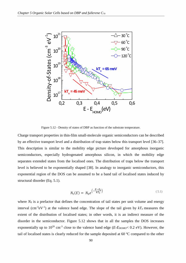
Chapter 5 Organic Solar Cells based on DBP and fullerene C70
90
0,2 0,3 0,4 0,5 0,6
1017
1018
1019
1020
1021
kTo = 45 meV
30 oC
60 oC
90 oC
120 oC
De
nsi
ty-o
f-S
tate
s (c
m-3
eV
-1)
E - EHOMO
(eV)
kTo = 65 meV
Figure 5.12 - Density of states of DBP as function of the substrate temperature.
Charge transport properties in thin-film small-molecule organic semiconductors can be described
by an effective transport level and a distribution of trap states below this transport level [36–37].
This description is similar to the mobility edge picture developed for amorphous inorganic
semiconductors, especially hydrogenated amorphous silicon, in which the mobility edge
separates extended states from the localised ones. The distribution of traps below the transport
level is believed to be exponentially shaped [38]. In analogy to inorganic semiconductors, this
exponential region of the DOS can be assumed to be a band tail of localised states induced by
structural disorder (Eq. 5.1).
where N0 is a prefactor that defines the concentration of tail states per unit volume and energy
interval (cm-3eV-1) at the valence band edge. The slope of the tail given by kTo measures the
extent of the distribution of localised states; in other words, it is an indirect measure of the
disorder in the semiconductor. Figure 5.12 shows that in all the samples the DOS increases
exponentially up to 1020 cm-3 close to the valence band edge (E-EHOMO< 0.2 eV). However, the
tail of localised states is clearly reduced for the sample deposited at 60 ºC compared to the other
./0 = .12343456+7 8 ( 5.1)

Chapter 5 Organic Solar Cells based on DBP and fullerene C70
91
substrate temperatures. The presence of these trap states in the band gap of the semiconductor
could act as traps and recombination centres and therefore could affect the position of the quasi
Fermi level position for holes in illumination [39]. The origin of these electronic trap states is
diverse and is still the subject of many investigations and discussions [36], [40], [41]. Some traps
(extrinsic) are related to contaminants and chemical defects with composition different than the
organic semiconductor and are associated with chemical impurities in the source material.
Another source of defects is related to the chemical instability inherent in many organic
compounds. It is well reported that organic molecules are reactive with oxygen and water [42].
Finally, some defects are associated with structural disorder (intrinsic traps) and are primary
introduced by the growing conditions [41], [43].
As has been mentioned before, in organic solar cells, it has been shown that the maximum
achievable value of VOC is determined by the energy offset between the LUMO of the acceptor
and the HOMO of the donor [44]. Experimentally, it has been found for a wide range of
materials the relationship qVOC = HOMODONOR –LUMOACCEPTOR – Δ [45]. The loss term (Δ) has
been related to the exciton binding energy of radiative or non-radiative recombination of polaron
pairs [47–48]. Despite the physical mechanisms contributing to the loss term Δ are still under
discussion, there is also a consensus that the distribution of localised states plays an important
role when determining VOC values [48]. The presence of tail states (broader DOS) causes a lower
effective energy gap and therefore a reduction of the VOC. In the particular case of a DBP donor,
photogenerated holes will prefer to occupy tail states rather than energy states in the HOMO
level, leading to a higher hole quasi-Fermi level position and, as a consequence, bringing the
average energy of electrons and holes closer together.
This phenomenon has already been studied in organic solar cells, both from the viewpoint of
numerical device simulation and experimental measurements. Blakesley et al. studied the
influence of energetic disorder on the VOC using numerical simulation [49]. They found that a
large increase of energetic disorder, or in other words broader DOS, causes a significant
reduction in VOC. Meanwhile, both JSC and FF also drop along with VOC.
5.3 p-i-n Organic Solar Cells based on DBP:C70
The p-i-n organic solar cell structure is presented in Chapter 3, section 3.3. In this section, the
results obtained from the characterisation of p-i-n solar cells are presented. The intrinsic layer (i-
layer) is composed by the coevaporation of donor and acceptor (at ratio 1:1). The i-layer

Chapter 5 Organic Solar Cells based on DBP and fullerene C70
92
thickness in p-i-n solar cells has strong influence in the performance. Increasing the thickness of
intrinsic layer can increase the efficiency caused by higher absorption; however, excess of
thickness reduce the efficiency due to recombination losses of free charge carriers. The
optimisation of active layer thickness taking into account the trade-off between absorption and
recombination is the objective of this section. Figure 5.13 shows the structure of the solar cells.
Figure 5.13 - Structure of p-i-n solar cell where i-layer is coevaporated at ratio donor – acceptor (1:1).
As previous section, the donor is DBP and the acceptor C70. In order to facilitate holes and
electrons collection, MoO3 has been used as hole transport layer and BCP as electron transport
layer inserted between the active layers and electrodes. The detailed configuration was
ITO/MoO3(3nm)/DBP:C70(1:1)(x nm)/BCP(8nm)/Al(150nm). The thickness of i-layer (x) varies
from 30 nm up to 70 nm. Figure 5.14 shows J-V curves of p-i-n cells with different i-layer
thickness. The substrate temperature during coevaporation of donor and acceptor were fixed at
60 ºC due to it is the optimum temperature for lower tail of DOS of DBP as demonstrated in
section 5.2.

Chapter 5 Organic Solar Cells based on DBP and fullerene C70
93
0,0 0,2 0,4 0,6 0,8-20
-18
-16
-14
-12
-10
-8
-6
-4
-2
0
Cu
rre
nt
De
nsi
ty (
mA
/cm
2)
Voltage (V)
30nm
40nm
60nm
70nm
90nm
100nm
Figure 5.14 - J–V Curves of p-i-n cells for different i-layer thickness.
The main photovoltaic parameters as a function of i-layer thickness are summarized in Table 5.1
and shown in Figure 5.15. Following, the influence of i-layer thickness in each parameter is
discussed.
Table 5.1 – Measurement results of the devices with various DBP:C70 thicknesses
Thickness (nm) PCE (%) FF (%) JSC (mA/cm2) VOC (V) 30 1.76 39 -6.2 0.73 40 2.82 36 -11.2 0.71 60 3.12 33 -14.1 0.65 70 2.90 27 -17.8 0.61 90 1.90 37 -8.4 0.61 100 1.01 27 -6.6 0.57

Chapter 5 Organic Solar Cells based on DBP and fullerene C70
94
-5
-10
-15
-2020 40 60 80 100
25
30
35
40
45
20 40 60 80 100
1
2
3
4
0,6
0,7
0,8Js
c (m
A/c
m2)
FF
(%
)
Thickness (nm)
PC
E (
%)
Vo
c (V
)
Figure 5.15 - Photovoltaic parameters of p-i-n organic solar cells versus i-layer thickness.
Short Circuit Current (JSC)
It was found that the JSC of p-i-n solar cells was increasing while the thickness of i-layer is
increasing up to 70 nm, indicating an efficient charge generation for this thickness. The
enhancing of JSC could be explained due to the increment of the absorption and the higher donor-
acceptor interface. On the other hand, the JSC starts to decrease when the thickness is higher than
70 nm. The JSC reduction could be attributed to geminate recombination of the excitions due to
the short exciton diffusion length. As a result, JSC has the highest value at 70 nm (17.84 mA/cm2)
and the lowest value was reached with thickness about 30 nm (6.19 mA/cm2).
Open Circuit Voltage (VOC)
The VOC value is falling whereas i-layer thickness is higher than 40nm, when VOC reaches the
highest value. As explained above, VOC value is related to the separation of the electron and hole

Chapter 5 Organic Solar Cells based on DBP and fullerene C70
95
quasi-Fermi levels under illumination. The recombination in open-circuit is typically assumed to
be dominated by bimolecular recombination. The higher i-layer thickness also implies higher
bimolecular recombination since the free charge carriers (electrons and holes) must to travel
longer distances up to the electrodes. Consequently, VOC decrease because of the higher
bimolecular recombination.
Fill Factor (FF)
The FF of p-i-n cells seems to decrease when i-layer thickness increase. However, no clear trend
is observed. This phenomena could be explained because of FF is affected by both
recombination mechanisms of organic solar cells. The maximum FF value is 39%, achieved by
i-layer thickness of 30 nm, and the lowest FF value is 27%, reached by i-layer thickness of 70
nm.
Power Conversion Efficiency (PCE)
The PCE of solar cells is influenced by FF, VOC and JSC. The optimum p-i-n solar cell based on
DBP:C70 (1:1) has been obtained for i-layer thickness. For higher values of i-layer thickness the
PCE decreases, mainly leaded by the diminution of VOC. The performance of p-i-n solar cell with
i-layer thickness of 40 nm is JSC = 11.20 mA/cm2, VOC = 0.81 V, FF = 0.43 and PCE of
3.93%.The PCE could be improved by optimising the volume ratio between the donor and
acceptor, most likely with higher a concentration of the acceptor C70, since the exciton lifetime in
fullerene domains is higher than in DBP domains [8].
External Quantum Efficiency (EQE)
The spectral analysis of p-i-n cells from wavelength of 300 to 850 nm was examined by
measuring the EQE curves (Figure 5.16). The EQE curves keep a good correspondence with the
JSC values measured (Figure 5.15). The highest area of EQE belongs to p-i-n cell with i-layer
thickness of 70 nm, which has also the highest JSC. Conversely, the lowest area belongs to p-i-n
cells with 30 nm and 100 nm of i-layer thickness. The JSC of both cells are similar which are
about 6.19 mA/cm2 and 6.57 mA/cm2.

Chapter 5 Organic Solar Cells based on DBP and fullerene C70
96
300 350 400 450 500 550 600 650 700 750 800 8500
10
20
30
40
50
60
70
80
90
100
Ext
ern
al
Qu
an
tum
Eff
icie
ncy
(%
)
Wavelength (nm)
Thickness (nm)
30nm
40nm
60nm
70nm
90nm
100nm
Figure 5.16 - EQE curves of p-i-n solar cells with different i-layer thicknesses.
Furthermore, the peak around 350–400 nm can be related to the C70 absorption; on the other
hand, the peaks around 550–650 nm belong to DBP absorption. The curve of p-i-n cell with 60
nm of i-layer thickness has tendency almost flat comparing with other cells.

Chapter 5 Organic Solar Cells based on DBP and fullerene C70
97
References
[1] W. M. Wang, H. D. Yang, J. S. Zhang, S. Li, X. R. Luo, S. L. Feng, “Influence of Substrate Temperature on Properties of Transition Materials from Amorphous to Microcrystalline Silicon Prepared by VHF-PECVD”, Adv. Mat. Res. 750 (2013) 1906.
[2] A. de Calheiros Velozo, G. Lavareda, C. Nunes de Carvalho, A. Amaral, “Thermal dehydrogenation of amorphous silicon deposited on c-Si: Effect of the substrate temperature during deposition”, Phys. Status Solidi C 9 (2012) 2198.
[3] J. Shirafuji, M. Kuwagaki, T. Sato, Y. Inuishi, “Effect of Substrate Temperature on Properties of Glow-Discharged Hydrogenated Amorphous Silicon” Jpn. J. Appl. Phys. 23 (1984) 1278.
[4] D. Fujishima, H. Kanno, T. Kinoshita, E. Maruyama, M. Tanaka, M. Shirakawa, K. Shibata, “Organic thin-film solar cell employing a novel electron-donor material” Sol. Energ. Mat. Sol. 93 (2009) 1029.
[5] M. Hirade, C. Adachi, “Small molecular organic photovoltaic cells with exciton blocking layer at anode interface for improved device performance”, Appl. Phys. Lett. 99 (2011) 153302.
[6] D. Yokoyama, Z. Qiang Wang, Y.-J. Pu, K. Kobayashi, J. Kido, Z. Hong, “High-efficiency simple planar heterojunction organic thin-film photovoltaics with horizontally oriented amorphous donors”, Sol. Energy Mater. Sol. Cells, 98 (2012) 472.
[7] Y. Zheng, W. J. Potscavage, T. Komino, M. Hirade, J. Adachi, C. Adachi, “Highly efficient bulk heterojunction photovoltaic cells based on C70 and tetraphenyldibenzoperiflanthene”, Appl. Phys. Lett. 102 (2013) 143304.
[8] X. Xiao, J. D. Zimmerman, B. E. Lassiter, K. J. Bergemann, S. R. Forrest, “A hybrid planar-mixed tetraphenyldibenzoperiflanthene/C70 photovoltaic cell”, Appl. Phys. Lett. 102 (2013) 073302.
[9] Z. Wang, D. Yokoyama, X. Wang, “Highly efficient organic p-i-n photovoltaic cells based on tetraphenyldibenzoperiflanthene and fullerene C70”, Energy Environ. Sci. 6 (2013) 249.
[10] B. Rand, D. Burk, S. Forrest, “Offset energies at organic semiconductor heterojunctions and their influence on the open-circuit voltage of thin-film solar cells”, Phys. Rev. B, 75 (2007) 115327.
[11] M. Kröger, S. Hamwi, J. Meyer, T. Riedl, W. Kowalsky, A. Kahn, “P-type doping of organic wide band gap materials by transition metal oxides: A case-study on Molybdenum trioxide”, Org. Electron. 10 (2009) 932.
[12] J. Meyer, K. Zilberberg, T. Riedl, A. Kahn, “Electronic structure of Vanadium pentoxide: An efficient hole injector for organic electronic materials”, J. Appl. Phys. 110 (2011) 033710.
[13] D. Y. Kim, J. Subbiah, G. Sarasqueta, F. So, H. Ding, Irfan, Y. Gao, “The effect of molybdenum oxide interlayer on organic photovoltaic cells”, Appl. Phys. Lett. 95 (2009) 093304.

Chapter 5 Organic Solar Cells based on DBP and fullerene C70
98
[14] M. T. Greiner, M. G. Helander, W.-M. Tang, Z.-B. Wang, J. Qiu, Z.-H. Lu, “Universal energy-level alignment of molecules on metal oxides”, Nat. Mater., 11 (2012) 76.
[15] M. Kroger, S. Hamwi, J. Meyer, T. Riedl, W. Kowalsky, A. Kahn, “Role of the deep-lying electronic states of MoO3 in the enhancement of hole-injection in organic thin films”, Appl. Phys. Lett. 95 (2009) 123301.
[16] Y. Zhou, T. Taima, Y. Shibata, T. Miyadera, T. Yamanari, Y. Yoshida, “Controlled growth of dibenzotetraphenylperiflanthene thin films by varying substrate temperature for photovoltaic applications”, Sol. Energy Mater. Sol. Cells 95 (2011) 2861.
[17] T. Sueyoshi, H. Fukagawa, M. Ono, S. Kera, N. Ueno, “Low-density band-gap states in pentacene thin films probed with ultrahigh-sensitivity ultraviolet photoelectron spectroscopy”, Appl. Phys. Lett. 95 (2009) 183303.
[18] O. Tal, Y. Rosenwaks, Y. Preezant, N. Tessler, C. Chan, A. Kahn, “Direct determination of the hole density of states in undoped and doped amorphous organic films with high lateral resolution”, Phys. Rev. Lett. 95 (2005) 256405.
[19] H. Matsui, A. S. Mishchenko, T. Hasegawa, “Distribution of localized states from fine analysis of electron spin resonance spectra in organic transistors”, Phys. Rev. Lett., 104 (2010) 056602.
[20] C. Krellner, S. Haas, C. Goldmann, K. P. Pernstich, D. J. Gundlach, B. Batlogg, “Density of bulk trap states in organic semiconductor crystals: Discrete levels induced by oxygen in rubrene”, Phys. Rev. B, 75 (2007) 245115.
[21] V. Nádaždy, R. Durný, J. Puigdollers, C. Voz, S. Cheylan, K. Gmucová, “Experimental observation of oxygen-related defect state in pentacene thin films”, Appl. Phys. Lett. 90 (2007) 092112.
[22] D. V. Lang, X. Chi, T. Siegrist, A. M. Sergent, A. P. Ramirez, “Amorphouslike density of gap states in single-crystal pentacene”, Phys. Rev. Lett. 93 (2004) 086802.
[23] G. Garcia-Belmonte, P. P. Boix, J. Bisquert, M. Lenes, H. J. Bolink, A. La Rosa, S. Filippone, N. Martín, “Influence of the intermediate density-of-states occupancy on open-circuit voltage of bulk heterojunction solar cells with different fullerene acceptors”, J. Phys. Chem. Lett., 1 (2010) 2566.
[24] T. Globus, H. C. Slade, M. Shur, M. Hack, “Density of deep bandgap states in amorphous silicon from the temperature dependence of thin film transistor current”, MRS Proceedings 336 (1994) 823.
[25] J. Puigdollers, A. Marsal, S. Cheylan, C. Voz, R. Alcubilla, “Density-of-states in pentacene from the electrical characteristics of thin-film transistors”, Org. Electron. 11 (2010) 1333.
[26] J. C. Blakesley, D. Neher, “Relationship between energetic disorder and open-circuit voltage in bulk heterojunction organic solar cells”, Phys. Rev. B 84 (2011) 075210.
[27] G. Garcia-Belmonte, “Temperature dependence of open-circuit voltage in organic solar cells from generation–recombination kinetic balance”, Sol. Energy Mater. Sol. Cells, 94 (2010) 2166.

Chapter 5 Organic Solar Cells based on DBP and fullerene C70
99
[28] S. R. Cowan, A. Roy, A. J. Heeger, “Recombination in polymer-fullerene bulk heterojunction solar cells”, Phys. Rev. B, 82 (2010) 245207.
[29] M. Pope, C. E. Swenberg, “Electronic Processes in Organic Crystals and Polymers”, Oxford University Press. 1999.
[30] C. Deibel, A. Wagenpfahl, V. Dyakonov, “Origin of reduced polaron recombination in organic semiconductor devices”, Phys. Rev. B, 80 (2009) 075203.
[31] C. Shuttle, B. O’Regan, A. Ballantyne, J. Nelson, D. Bradley, J. Durrant, “Bimolecular recombination losses in polythiophene: Fullerene solar cells”, Phys. Rev. B 78 (2008) 113201.
[32] G. Juška, G. Sliaužys, K. Genevičius, K. Arlauskas, A. Pivrikas, M. Scharber, G. Dennler, N. Sariciftci, R. Österbacka, “Charge-carrier transport and recombination in thin insulating films studied via extraction of injected plasma”, Phys. Rev. B, 74 (2006) 115314.
[33] J.-T. Shieh, C.-H. Liu, H.-F. Meng, S.-R. Tseng, Y.-C. Chao, S.-F. Horng, “The effect of carrier mobility in organic solar cells”, J. Appl. Phys. 107 (2010) 084503.
[34] W. Tress, K. Leo, M. Riede, “Optimum mobility, contact properties, and open-circuit voltage of organic solar cells: A drift-diffusion simulation study”, Phys. Rev. B 85 (2012) 155201.
[35] Y. Terao, H. Sasabe, C. Adachi, “Correlation of hole mobility, exciton diffusion length, and solar cell characteristics in phthalocyanine/fullerene organic solar cells”, Appl. Phys. Lett. 90 (2007) 103515.
[36] W. L. Kalb, S. Haas, C. Krellner, T. Mathis, B. Batlogg, “Trap density of states in small-molecule organic semiconductors: A quantitative comparison of thin-film transistors with single crystals”, Phys. Rev. B 81 (2010) 155315.
[37] V. I. Arkhipov, P. Heremans, E. V. Emelianova, G. J. Adriaenssens, H. Bässler, “Charge carrier mobility in doped semiconducting polymers”, Appl. Phys. Lett. 82 (2003) 3245.
[38] K. Celebi, P. J. Jadhav, K. M. Milaninia, M. Bora, M. A. Baldo, “The density of states in thin film copper phthalocyanine measured by Kelvin probe force microscopy”, Appl. Phys. Lett. 93 (2008) 083308.
[39] G. Horowitz, R. Hajlaoui, P. Delannoy, “Temperature dependence of the field-effect mobility of sexithiophene. Determination of the density of traps”, Journal de Physique III, 5 (1995) 355.
[40] J. A. Carr, S. Chaudhary, “The identification, characterization and mitigation of defect states in organic photovoltaic devices: a review and outlook”, Energy Environ. Sci. 6 (2013) 3414.
[41] L. G. Kaake, P. F. Barbara, X.-Y. Zhu, “Intrinsic charge trapping in organic and polymeric semiconductors: a physical chemistry perspective”, J. Phys. Chem. Lett. 1 (2010) 628.
[42] D. Knipp, J. E. Northrup, “Electric-Field-Induced Gap States in Pentacene”, Adv. Mater. 21 (2009) 2511.

Chapter 5 Organic Solar Cells based on DBP and fullerene C70
100
[43] T. S. Ripolles, A. Guerrero, G. Garcia-Belmonte, “Polymer defect states modulate open-circuit voltage in bulk-heterojunction solar cells”, Appl. Phys. Lett., 103 (2013) 243306.
[44] C. J. Brabec, A. Cravino, D. Meissner, N. S. Sariciftci, T. Fromherz, M. T. Rispens, L. Sanchez, J. C. Hummelen, “Origin of the open circuit voltage of plastic solar cells”, Adv. Funct. Mater. 11 (2001) 374.
[45] M. C. Scharber, D. Mühlbacher, M. Koppe, P. Denk, C. Waldauf, A. J. Heeger, C. J. Brabec, “Design rules for donors in bulk-heterojunction solar cells-towards 10% energy-conversion efficiency”, Adv. Mater. 18 (2006) 789.
[46] K. Vandewal, K. Tvingstedt, A. Gadisa, O. Inganäs, J. V. Manca, “Relating the open-circuit voltage to interface molecular properties of donor: acceptor bulk heterojunction solar cells”, Phys. Rev. B 81 (2010) 125204.
[47] N. C. Giebink, B. E. Lassiter, G. P. Wiederrecht, M. R. Wasielewski, S. R. Forrest, “Ideal diode equation for organic heterojunctions. II. The role of polaron pair recombination”, Phys. Rev. B, 82 (2010) 155306.
[48] G. Garcia-Belmonte, “Carrier recombination flux in bulk heterojunction polymer: fullerene solar cells: Effect of energy disorder on ideality factor”, Solid. State. Electron., 79 (2013) 201.
[49] J. C. Blakesley, N. C. Greenham, “Charge transfer at polymer-electrode interfaces: The effect of energetic disorder and thermal injection on band bending and open-circuit voltage”, J. Appl. Phys. 106 (2009) 034507.

101
6. Model for charge carrier collection efficiency in Organic Solar Cells
In this Chapter, an equivalent circuit for organic solar cells is presented. It is based on the
classic combination of a diode with an exponential current–voltage characteristic, parasitic
series and parallel resistances, a photogenerated current source, plus a new term representing
recombination losses in the active layer of the device. The model clearly separates technological
issues (series and parallel resistance) from effects related to the physics of the device
(recombination losses). It also allows an effective μτ product in the active layer of the device to
be determined, characterising its state of degradation.
6.1 Model for Organic Solar Cell
The use of equivalent circuits is a convenient way to describe the electrical behaviour of
electronic devices. Therefore, an equivalent circuit model is helpful in the understanding and
optimisation of solar cells by providing a quantitative estimate for losses in the device. The
conventional circuit model developed in the context of photovoltaic solar cells is presented in
Chapter 3 and shown in Figure 6.1[1]. According to this equivalent circuit, the J–V characteristic
can be expressed by an implicit equation (Eq. 6.1). This model essentially consists of a current
source shunted by a diode. These two elements correspond to generation and loss of photocurrent
in the device. The resistances RS and RP can be considered to be “parasitic” circuit elements,
introduced to describe the behaviour of real solar cells with their technological limitations. This
model has been used to interpret results obtained with organic solar cells as well [2–4]. In view
of the fact that photovoltaic response in organic solar cells is considerably different from that in
inorganic solar cells, the modification of conventional solar cell circuit model is discussed in this
Chapter.

Chapter 6 Model for charge carrier collection efficiency in Organic Solar Cells
102
Figure 6.1 - Equivalent circuit for standard solar cell.
6.2 Introduction to the Variable Illumination Measurement method
The standard equivalent circuit superposes a photocurrent source on the electrical characteristic
of the dark diode. Nonetheless, it is important to note that the photogeneration of electrons and
holes within the solar cell will change the carrier concentration at every point. Thus, in principle,
a new solution for the drift-diffusion differential equations throughout the whole device would
be required. However, such a simple superposition of a dark diode and a photocurrent source is
indeed valid and can be theoretically justified for crystalline solar cells, consisting of pn-diodes.
The theoretical justification [5] is based on the linear form of the drift-diffusion differential
equations for minority carriers, within the p- or n-type bulk regions of the pn-diode.
However, it is well known that the main part of the photovoltaic generation in solar cells with a
p-i-n structure occurs in the active i-layer, as in the case of amorphous silicon solar cells. As a
striking example, the curves for different illumination levels usually all meet at a single point in
the first quadrant [6], which has been called collection voltage (VC). This fact can only be
reconciled with the simple equivalent circuit of Fig. 6.2 by including an additional loss term,
which increases strongly with the forward voltage. Such a loss term takes into account the
recombination losses in the active layer of the device. Then, this term has to be considered in the
implicit equation (Eq. 6.2). In this section, we propose a method to gain valuable information
about the device operation and, in particular, the recombination term. The basic idea is to
measure the J(V) curve over a wide range of illumination levels, rather than at a fixed level of
1exp
p
s
T
soph R
JRV
nV
JRVJJJ
−+
−
−+−= (6.1)

Chapter 6 Model for charge carrier collection efficiency in Organic Solar Cells
103
one sun. For that reason, we have called it the Variable Illumination Measurement (VIM)
method.
Figure 6.2 - Equivalent circuit for solar cell with recombination term.
6.2.1 Parameters of the model
We have used the standard characterisation procedure for solar cells that consists of measuring
the curve at a given illumination level as it shown in Figure 6.3. The resulting data may be
condensed into the six characteristic parameters which are:
1) the short circuit current ISC;
2) the open circuit voltage VOC;
3) the fill factor FF;
4) the efficiency η;
5) the “open circuit resistance” ROC, which at a high illumination level may be related to the
series resistance ;
6) and the “short circuit resistance” RSC, which at a low illumination level may be related to
the parallel resistance
The latter two parameters are key parameters for the present treatment; they are defined as the
reciprocal slopes of the J-V curve.
+
_
V Rp
Rs J
Jdio
Jph Jrec
Jleak
1exp rec
p
s
T
soph J
R
JRV
nV
JRVJJJ +−+
−
−+−= (6.2)

Chapter 6 Model for charge carrier collection efficiency in Organic Solar Cells
104
Dynamic resistances:
Open circuit resistance
Short circuit resistance
Figure 6.3 - J–V curve of a p-i-n solar cell. Apart from the standard photovoltaic parameters (JSC, VOC and FF), we also consider the dynamic resistance of the device evaluated at short-circuit and open-circuit conditions (RSC and
ROC).
The logarithmic variation on the illumination intensity can be classified in five distinct levels,
each one of them with a characteristic J(V) curve (Figure 6.3):
Figure 6.4 - Five illumination levels used in the VIM method, where Level C ≈1 sun. Figure adapted from [7].
Level A) At very low illumination levels, the J(V) curve is completely shaped by the
parallel resistance RP, which determines the values of both RSC and ROC. The value of RP
limits the VOC the FF is equal to a minimum 0.25.
Level B) By increasing the illumination, the RP still determines the RSC value, which
shapes the short circuit region of the measurement. The J(V) curve at forward voltage is
0=∂∂=
VSC J
VR
0=∂∂=
JOC J
VR
A B C D E
RSC = ROC = RP RSC = RP J(V) ≠ f(RSC,ROC) ROC = RS ROC = RSC =RS
(6.3)
(6.4)

Chapter 6 Model for charge carrier collection efficiency in Organic Solar Cells
105
already shaped by the physics of the device. Both the VOC and the FF progressively
increase.
Level C) In this regime, the J(V) curve is not affected by neither RS nor RP but by the
physics of the device. The FF reaches a maximum and the device is at its optimum
operating point (≈1 sun).
Level D) Further increasing the illumination level, the ROC vale equals the series
resistance RS, which begins to shape the open circuit region of the J(V) curve, while the
rest remains shaped by the physics of the device. While the VOC still increases, the FF
starts to decrease.
Level E) At very high illumination levels the J(V) is completely shaped by the RS value,
which determines both RSC and ROC. At this level, VOC reaches a maximum while the FF
is again at a minimum 0.25.
6.2.2 Assumptions for the model
A few assumptions and modelling simplifications were done, many of them based upon the
experience in amorphous silicon solar cells, but also extendable to organic solar cells with p-i-n
structure:
a) Charge collection in p-i-n solar cells is mainly a drift-driven process, while diffusion
plays a minor role [8]. This assumption is particularly true around the short circuit
condition, as it has been justified in the literature [9–10].
b) Several works also support that the J–V curve is affected by a first-order recombination
process from the short-circuit condition to around the maximum power point [11–12].
Recently, this behaviour has been explained considering a monomolecular recombination
process through localised states near the interface between donor and acceptor domains
[13–14].
c) The electric field 0 is constant through the intrinsic layer. This approximation has been
widely used to describe the behaviour of inorganic thin film solar cells based on
amorphous silicon due to the low fixed charge density in their intrinsic active layers [8,
15–16]. Although the relevance of fixed charge densities in organic semiconductors is
still subject of discussion [17–18], a constant electric field approximation is often
assumed in the literature considering the rather thin active layer of these devices (<100

Chapter 6 Model for charge carrier collection efficiency in Organic Solar Cells
106
nm) [9, 19]. The electrostatic potential on the active layer is given by the difference
between the built-in voltage across the electrodes (Vbi) and the applied voltage V. Thus,
the intensity of the electric field within the active layer of thickness L can be calculated
as:
6.2.3 Effective mobility-lifetime product (μτeff) of charge carriers
Under the previous assumptions (drift-driven collection, monomolecular recombination and
constant electric field), a compact analytical expression for the current density near the short-
circuit condition can be used [8] (Eq. 6.6):
where q is the elementary charge and G the effective generation rate of charge carriers per unit
volume, which considers only those excitons which are effectively dissociated. A constant
generation rate is a good approximation for the typically thin active layers of p-i-n solar cells
illuminated under the AM1.5 spectra. The collection length lc in Eq. 6.6 is defined as the sum of
the corresponding drift lengths for electrons (ln = μnτn E) and holes (lp = μpτp E), that is, lc = le +
lh. The collection length is interpreted as the maximum distance these charges separate apart
driven by the electric field before recombining.
Then, by introducing an effective μτeff product and taking into account Eq. (6.5), the collection
length lc can be written as:
where μτeff = μnτn + μpτp.
The validity of Eq. 6.6 is limited to small applied voltages, since it does not consider charge
carrier injection by the electrodes. This means that the contribution of the diode term and shunt
resistance to the current density must be much lower than the total photogenerated current
density reduced by the recombination term:
0 = 9: − # ( 6.5)
= ;<=> ?1 − 1AB C− #=>DE ( 6.6)
=> = FF + HH0 = FII 9: − # (6.7)
≈ KH − LF> (6.8)

Chapter 6 Model for charge carrier collection efficiency in Organic Solar Cells
107
Anyhow, Eq. 6.6 indeed describes the J–V curve under illumination at moderate applied
voltages. For long collection lengths compared to the active layer thickness, it can be
approximated by:
where we can identify the photogenerated current density KH = ;<#, that we would obtain if all
the charge carriers were collected in the external circuit. Eq. 6.9 can be particularised at the
short-circuit condition to obtain an expression for JSC:
where we have introduced the short-circuit collection length lco = μτeff Vbi / L, that is the
collection length given by Eq. 6.7 evaluated at zero applied voltage. According to Eq. 6.9, the
collection efficiency at moderate applied voltages can be calculated as:
Eq. 6.11 states that the fraction of the photogenerated current that recombines into the active
layer is given by the ratio of L/2 to lc. This result can be physically interpreted considering that
the mean distance that charge carriers have to move in order to reach its corresponding electrode
is actually half of the thickness of the active layer. Then, we finally obtain an analytical
expression for the recombination term valid for moderate applied voltages:
Finally, according to definition of RSC, by evaluating the derivative MLF> M⁄ |P> we obtain the
following expression for RSC:
This last equation gives a direct relation between the collection voltage VC and the physical
mechanisms governing charge carrier collection [20]:
≈ ;<# Q1 − # 2R=> S (6.9)
&T = KH Q1 − # 2R=>US (6.10)
η> = 1 − # 2R=> (6.11)
LF> = KH Q# 2R=> S = KH # 2⁄FII9: − (6.12)
VP> = C2FII9:# − 1D 9:P> = TP> (6.13)

Chapter 6 Model for charge carrier collection efficiency in Organic Solar Cells
108
6.3 Results for p-i-n small-molecule solar cells based on DBP/C70
The VIM method has been used to study the quality of the intrinsic layer of organic solar cells
with pin structure. The solar cells used in this study have the following structure:
glass/ITO/MoO3/DBP:C70(X nm)/BCP(8 nm)/Al(150 nm). The i-layer (DBP:C70) thickness was
30nm and 40 nm for two different devices.
Figure 6.5 - Structure of p-i-n solar cell used for VIM analysis.
A simple graphical interpretation for the collection voltage is obtained when analysing the J(V)
curves for the different illumination levels applied to the solar cells under study (Figure 6.6). The
VC value can then be obtained as that single point where all 1/RSC slopes meet when extrapolated
into the x axis. This fact also implies that, under reverse bias conditions, the short-circuit current
approaches the total photogenerated current (JSC ≲ Jph) [21].
T = Q =>U# 2R 1S 9: (6.14)

Chapter 6 Model for charge carrier collection efficiency in Organic Solar Cells
109
-10
-8
-6
-4
-2
00,0 0,5 1,0 1,5 2,0 2,5 3,0 3,5
Voltage (V)
Cu
rre
nt
De
nsi
ty (
mA
/cm
2)
Vc = 3,07 V
-40
-30
-20
-10
00,0 0,2 0,4 0,6 0,8 1,0 1,2 1,4
Voltage (V)
Cu
rre
nt
De
nsi
ty (
mA
/cm
2)
Vc = 1.42 V
Figure 6.6 - J -V curves for the p-i-n organic solar cells measured with VIM method. The collection voltage VC is
obtained by the x-axis intersection of the 1/RSC slopes. i-layer thickness of 40nm (left) and 30nm (right)
After extracting the VC value from experimental VIM data (Figure 6.6) and considering that Vbi ≈
Wanode − Wcathode = 0.7 V, the μτeff of each solar cell can be calculated (Table 6.1). These values
are comparable to those reported in the literature for similar devices [13][22–23].
Table 6.1 Values for the carrier collection process obtained from the VIM analysis.
i-layer thickness (nm)
VC (V)
μτeff (cm2/V)
lC (nm) ηC
Jrec (mA/cm2)
40 3.07 3.07x10⁻¹⁰ 173.5 88% 1.46 30 1.42 3.56x10⁻¹¹ 50.6 70% 2.60
These results give us an insight on the carrier transport process in the active layer, which can be
related to its quality. For the device with a 40 nm thick i-layer, the higher μτeff value indicates
lower recombination losses and a better current extraction into the electrodes. Namely, the
collection length (at short circuit conditions) is almost 4 times larger than the active layer. This
leads to a carrier collection efficiency of 88%, meaning that only 12% of the photogenerated
current is lost because of recombination (Jrec). On the other hand, for the 30 nm thick i-layer, the
lower μτeff value indicates a poorer carrier transport quality of the device. Consequently, the
collection efficiency is limited to a value of 70% because of the higher recombination term. Note
that the collection efficiency depends on the active layer quality but also on its thickness, which
influences the strength of the electric field. By contrast, the μτeff value is only characteristic of the
active layer quality. The differences observed between these two devices, fabricated under very
similar deposition conditions, could be related to the fast degradation of non- encapsulated
devices in ambient.

Chapter 6 Model for charge carrier collection efficiency in Organic Solar Cells
110
6.4 Degradation of p-i-n Organic Solar Cells
One of the main drawbacks of organic solar cells is that they are prone to degradation in the
presence of oxygen and humidity, making necessary the encapsulation under transparent
polymer membranes or glass to maintain their electronic properties.
An insight on the causes of solar cell degradation can be obtained by applying the VIM method
for a long time after the fabrication. Since RS, RP and μτeff are related to specific quality aspects
of the cell, a distinction can be made between degradation of the i-layer and other parts of the
cell, such as the metal contacts.
For an organic p-i-n solar cell with the following structure:
glass/ITO/MoO3/DBP:C70(30nm)/BCP(8nm)/Al(150nm), VIM measurements were done after
cell fabrication and every 5 hours. The cell remained under nitrogen atmosphere, in a fixed
position and under dark conditions between these measurements. Table 6.2 shows the
performance parameters for one measure of the VIM data.
Table 6.2 Main performance parameters of p-i-n organic solar cell based on DBP:C70(1:1) with i-layer thickness of
30 nm at t=0 h and t=30 h.
Time PCE
(%)
FF
(%)
PMAX
(mW/cm2)
JSC
(mA/cm2)
VOC
(V)
Diode n
0 h 1.60 38 2.1 7.77 0.71 1.41
30 h 0.66 35 0.86 3.60 0.68 1.40
Even though the cell was kept under N2 atmosphere and it was only illuminated every 5 hours
during data acquisition, the decrease in the conversion efficiency is substantial (59%). The
largest degradation comes from a JSC drop of 54%, while FF drops only by 7% and there is also
a very slight decrease in the VOC. This is consistent with experimental results reported by [24],
where similar losses in JSC and PCE occurred when measuring the cell under ambient conditions.
Almost no change was observed in the ideality factor n, although reported degradation tests have
signalled an increase as a possible reason for loss of efficiency [25].
Analysis of the series resistance RS shows an important increment, somewhat explaining the
decrease in FF (Figure 6.7). This is attributed to degradation outside i-layer, such as corrosion or

Chapter 6 Model for charge carrier collection efficiency in Organic Solar Cells
111
delamination of the contacts, leading to a drop in conductivity and a change in the work function.
This effect has also been reported in previous studies [26].
0 5 10 15 20 25 30
10
15
20
25
30
35
Rs
(Ω c
m2)
time (h)
Figure 6.7 - Evolution of series resistance of p-i-n solar cells based on DBP:C70 (1:1)
Figure 6.8 shows how μτeff also decreases with time, clearly representative of a loss in carrier
mobility and/or lifetime. Following the same explanation as in [13], the larger than expected
drop in JSC and FF cannot attribute to the decrease of μτeff (Figure 6.8), indicating that some
other factor (different from ηC) contributes to the drop of the power conversion efficiency. This
major degradation could be due to a loss of optical absorbance in the active layer (ηA), a loss in
the exciton diffusion capability (ηED), or a loss in the exciton transfer into carriers (ηCT).
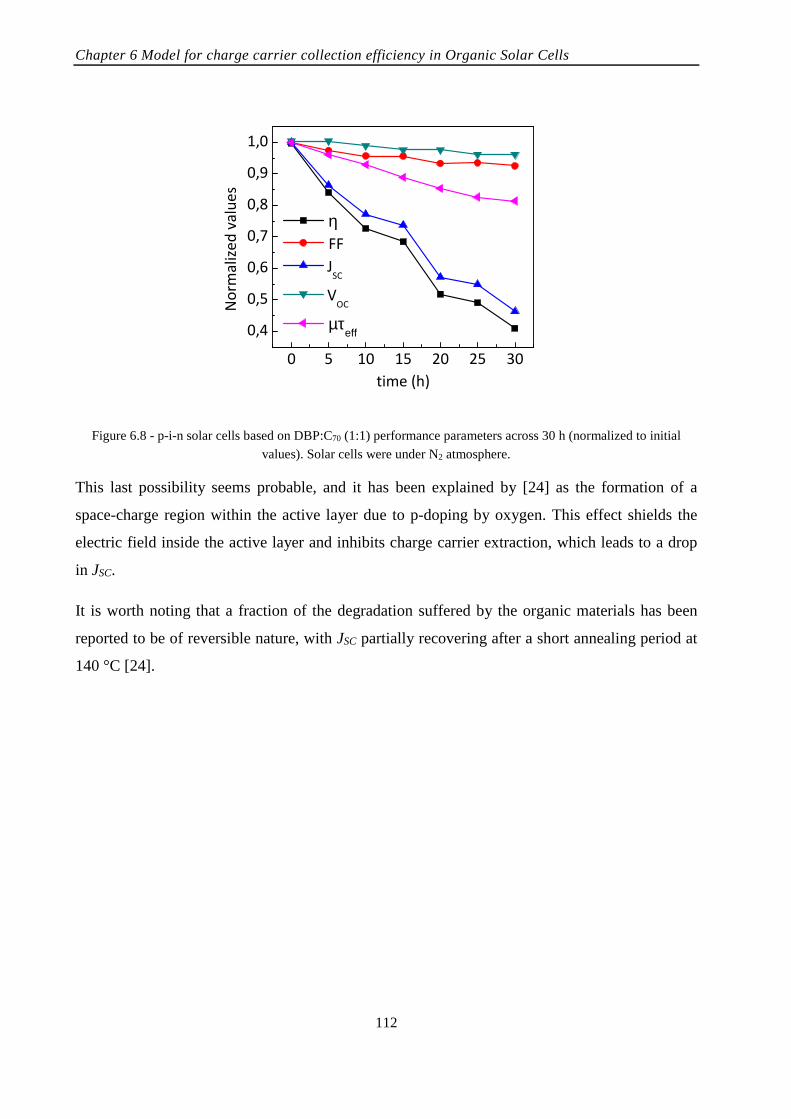
Chapter 6 Model for charge carrier collection efficiency in Organic Solar Cells
112
0 5 10 15 20 25 30
0,4
0,5
0,6
0,7
0,8
0,9
1,0
No
rma
lize
d v
alu
es
time (h)
η FF
JSC
VOC
µτeff
Figure 6.8 - p-i-n solar cells based on DBP:C70 (1:1) performance parameters across 30 h (normalized to initial
values). Solar cells were under N2 atmosphere.
This last possibility seems probable, and it has been explained by [24] as the formation of a
space-charge region within the active layer due to p-doping by oxygen. This effect shields the
electric field inside the active layer and inhibits charge carrier extraction, which leads to a drop
in JSC.
It is worth noting that a fraction of the degradation suffered by the organic materials has been
reported to be of reversible nature, with JSC partially recovering after a short annealing period at
140 °C [24].

Chapter 6 Model for charge carrier collection efficiency in Organic Solar Cells
113
References
[1] S. M. Sze, “Physics of Semiconductor Devices”, second ed., Wiley, New York.
[2] H. Hoppe, N. S. Sariciftci “Organic solar cells: An overview”, J. Mater. Res. 19 (2004) 1924.
[3] S. Yoo, B. Domercq, B. Kippelen, “Efficient thin-film organic solar cells based on pentacene/C60 heterojunctions”, Appl. Phys. Lett. 85 (2004) 5427.
[4] J. M. Nunzi, “Organic photovoltaic materials and devices”, C. R. Physique 3 (2002) 523.
[5] H. G. Wagemann, H. Estrich, Grundlagen der photovoltaischen Energiewandlung. Stuttgart, Germany: Teubner, (1994).
[6] W. Kusian, H. Pfleiderer, W. Jürgens, “Buffer layer and light degradation of a-Si pin solar cells,” Proc. 9th E.C. Photovoltaic Solar Energy Conf. (1989) 52.
[7] J. Merten, C. Voz, A. Muñoz, J. Asensi, J. Andreu, “The role of the buffer layer in the light of a new equivalent circuit for amorphous silicon solar cells”, Sol. Energy Mater. Sol. Cells 57 (1999) 153.
[8] R. Crandall, “Modeling of thin film solar cells: Uniform field approximation”, J. Appl. Phys. 54 (1983) 7176.
[9] P. Schilinsky, C. Waldauf, J. Hauch, C.J. Brabec, “Simulation of light intensity dependent current characteristics of polymer solar cells”, J. Appl. Phys. 95 (2004) 2816.
[10] S. R. Cowan, R. A. Street, S. Cho, A. J. Heeger, “Transient photoconductivity in polymer bulk heterojunction solar cells: Competition between sweep-out and recombination”, Phys. Rev. B 83 (2011) 035205.
[11] L. Liu, G. Li, “Investigation of Recombination Loss in Organic Solar Cells by Simulating Intensity-Dependent Current-Voltage Measurements”, Sol. Energy Mater. Sol. Cells 95 (2011) 2557.
[12] S. R. Cowan, A. Roy, A. J. Heeger, “Recombination in polymer-fullerene bulk heterojunction solar cells”, Phys. Rev. B 82 (2010) 245207.
[13] R. A. Street, M. Schoendorf, A. Roy, J. H. Lee, “Interface state recombination in organic solar cells”, Phys. Rev. B 81 (2010) 205307.
[14] R. A. Street, A. Krakaris, S.R. Cowan, “Recombination Through Different Types of Localized States in Organic Solar Cells”, Adv. Funct. Mater. 22 (2012) 4608.
[15] J. Hubin, A. V. Shah, “Effect of the recombination function on the collection in a p-i-n solar cell” Philos. Mag. Part B 72 (1995) 589.
[16] J. Merten, J. M. Asensi, C. Voz, A. V. Shah, R. Platz, J. Andreu, “Improved Equivalent Circuit and Analytical Model for Amorphous Silicon Solar Cells and Modules”, IEEE Trans. Electron. Devices 45 (1998) 423.
[17] J. Bisquert, G. Garcia-Belmonte, “On Voltage, Photovoltage, and Photocurrent in Bulk Heterojunction Organic Solar Cells”, J. Phys. Chem. Lett. 2 (2011) 1950.

Chapter 6 Model for charge carrier collection efficiency in Organic Solar Cells
114
[18] Z. Liang, B. A. Gregg, “Compensating poly(3-hexylthiophene) reveals its doping density and its strong exciton quenching by free carriers”, Adv. Mater. 24 (2012) 3258.
[19] P. Kumar, S. C. Jain, V. Kumar, S. Chand, R. P. Tandon, “A model for the current–voltage characteristics of organic bulk heterojunction solar cells”, J. Phys. D Appl. Phys. 42 (2009) 055102.
[20] C. Voz, J. Puigdollers, J. Asensi, S. Galindo, S. Cheylan, R. Pacios, P. Ortega, R. Alcubilla, “Analysis of the dynamic short-circuit resistance in organic bulk-heterojunction solar cells: relation to the charge carrier collection efficiency”, Org. Electron. 14 (2013)1643.
[21] C. Hof, N. Wyrsch, A. Shah, “Influence of electric Field distortion and i-layer quality on the collection function of drift-driven a-Si:H solar cells”, J. Non-Cryst. Solids 266 (2000) 1114.
[22] C. Deibel, “Charge carrier dissociation and recombination in polymer solar cells”, Phys. Status Solidi A 206 (2009) 2731.
[23] A. Pivrikas, N. Sariciftci, G. Juska, R. Osterbacka, “A Review of Charge Transport and Recombination in Polymer/Fullerene Organic Solar Cells” Prog. Photovolt: Res. Appl, 15 (2007) 677.
[24] A. Seemann, T. Sauermann, C. Lungenschmied, O. Armbruster, H. Egelhaaf, J. Hauch, “Reversible and irreversible degradation of organic solar cell performance by oxygen”, Sol. Energy 85 (2011) 1238.
[25] P. Schilinsky, “Loss Analysis of the Power Conversion Efficiency of Organic Bulk Heterojunction Solar Cells”, PhD Thesis, Oldenburg University, 2005.
[26] R. A. Street, P. P. Khlyabich, B. C. Thompson, “Electrical characterization of organic solar cell contact degradation resulting from ambient exposure”, Org. Electron., 14 (2013) 2932.

115
7. Conclusions and Outlook Organic solar cells have gathered much attention last decades, mainly since 2005 when its record
efficiencies have increased exponentially. However, their interest seems to have diminished
since 2012, when was reported the highest power conversion efficiency of OSC with 12%. It is
worth to mention that most of the research labs working on dye and organic solar cells have
shifted its activities to perovskites solar cells.
This thesis deals with the research on organic solar cells based on small-molecules
semiconductors. Organic solar cells were fabricated by thermal evaporation on glass substrates.
All the fabrication process were done in inert conditions. The materials used in this thesis were
tetraphenyldibenzoperiflanthene as donor material and fullerene C70 as acceptor material.
In the first results of this thesis, we focus on the influence of the density of states of the donor
layer on the characteristic parameters of organic solar cells. For that reason, a study of the
variation in performance of solar cells where the donor material was deposited at different
substrate temperatures were done. This work demonstrated that the optimum substrate
temperature for this kind of solar cells was 60 ºC, since the tail of localised states is clearly
reduced for the sample deposited at 60 ºC compared to the other substrate temperatures. This
effect leads to an enhancement of the open circuit voltage in the solar cell. Further, organic solar
cells with p-i-n structure, where the intrinsic layer is obtained by coevaporation of donor and
acceptor, were analysed. This work demonstrated that the optimum thickness of the intrinsic
layer of the p-i-n solar cell based on DBP and fullerene C70 is 40 nm.
In the second part, an equivalent circuit for organic solar cells with a new term representing
recombination losses in the active layer of the organic solar cell is considered. The model allows
obtaining of an effective mobility-lifetime product in the active layer of the device to be
determined, characterising its state of degradation. The degradation of p-i-n organic solar cells
based on DBP and C70 were analysed. The main factor of the degradation of solar cells was not
its intrinsic layer, indicating that some other factor contributes strongly to the decrease of the

Conclusions and Outlook
116
power conversion efficiency. Due to the increment of series resistance, the degradation of this
kind of solar cells could be attributed to the contacts.
117
APPENDIX I: Electrical Characterisation of Organic Semiconductors from OTFT In this appendix detailed information about fabrication and characterisation of organic Thin-
Film Transistors (OTFTs) can be found. In the framework of this thesis, OTFTs have been used
to characterise the electrical properties of the organic semiconductors used in the fabrication of
the organic solar cells. In particular, we focused on the determination of the field-effect mobility
and on the estimation of the density of states (DOS) of localised states in the band-gap of the
semiconductor.
A_I.1 Introduction
First OTFTs were based on polymers like polyacetylene [1–2] and polythiophene [3], these
transistors had very low mobilities, below than 10-5cm2/Vs. First OTFT based on polymers with
high mobility (μ = 0.2 cm2/Vs) was reported by Fuchigami et al. in 1993 [4], but with low ON-
OFF current ratio. On the other hand, the first small-molecule OTFT based on sexithiophene was
reported in 1989 and had a mobility in order of 10-3–10-2 cm2/Vs [5]. Further improvement in
performance was achieved in 1997 with first vacuum sublimed pentacene molecule OTFT, with
mobility of 0.7 cm2/Vs [6]. Alternatively, the first OTFT based on solution-processed conjugated
polymer (P3HT) was reported in 1998, having with high mobility (0.1 cm2/Vs) and high ON-
OFF current ratio [7].
Tuning of molecular structure it is possible to optimise a determinate function and achieve a
performance enhancement. In addition, OTFTs are based on naturally abundant and sustainable
elements. On the other hand, the fabrication process by solution-processing is compatible with
large area and flexible devices. These advantages of OTFTs lead an increasing interest to use it
for applications such as smart cards, identification (ID) tags and flexible displays [8]. However,
the goal of use OTFT in this thesis is to characterise electrically organic semiconductor
molecules for its use in small-molecule solar cells. Following, the fabrication process and
characterisation details are exposed.

APPENDIX I: Electrical Characterisation of Organic Semiconductors from OTFT
118
A_I.2 Fabrication of OTFT
OTFTs were fabricated using the same experimental set-up used to fabricate the solar cells.
Since we want to correlate the properties of TFTs with OSC, the parameters to deposit organic
semiconductor were the same than the used for solar cells fabrication. Electrical properties
obtained when measuring TFT corresponds to longitudinal (planar) conductivity between two
electrodes (drain and source). Of course, this is not the ideal situation to compare with solar
cells, in which conductivity of the carriers between electrodes (anode and cathode) is essentially
transversal.
The structure of the fabricated TFT is shown in Figure A 1. An inverted-staggered (top contact,
bottom gate) geometry was choose. Crystalline silicon was used as a substrate. Thermally-grown
silicon dioxide (SiO2) 100-nm thick was used as a dielectric.
Top contact geometry is preferred to the bottom contact geometry, due to the easiness when
contact electrodes. Moreover, it has been reported that in top contact geometry devices perform
better due to lower contact resistance between electrodes and conductance channel.
Figure A 1 - Inverted-staggered (top contact) OTFT
Crystalline silicon is commonly used as a substrate and a gate electrode for OTFTs and leads the
great advantage of easily growth of silicon oxide (SiO2) as insulator (Figure A 2), which has well
known dielectric properties in the field of microelectronics and its flat surface ideal to deposit
organic layers. The thermal oxidation of silicon consists in a chemical reaction of surface of the
silicon wafer and an oxidant. The oxidant could be oxygen (dry oxidation) or water vapour (wet
oxidation). To facilitate the reaction should work with furnaces at high temperatures in the order
of 800–1100ºC, depending on the speed and thickness desired. Thermal oxidation was carried
out in clean room facilities of Universitat Politècnica de Catalunya inside a furnace at 1000ºC
with oxygen as the oxidant.
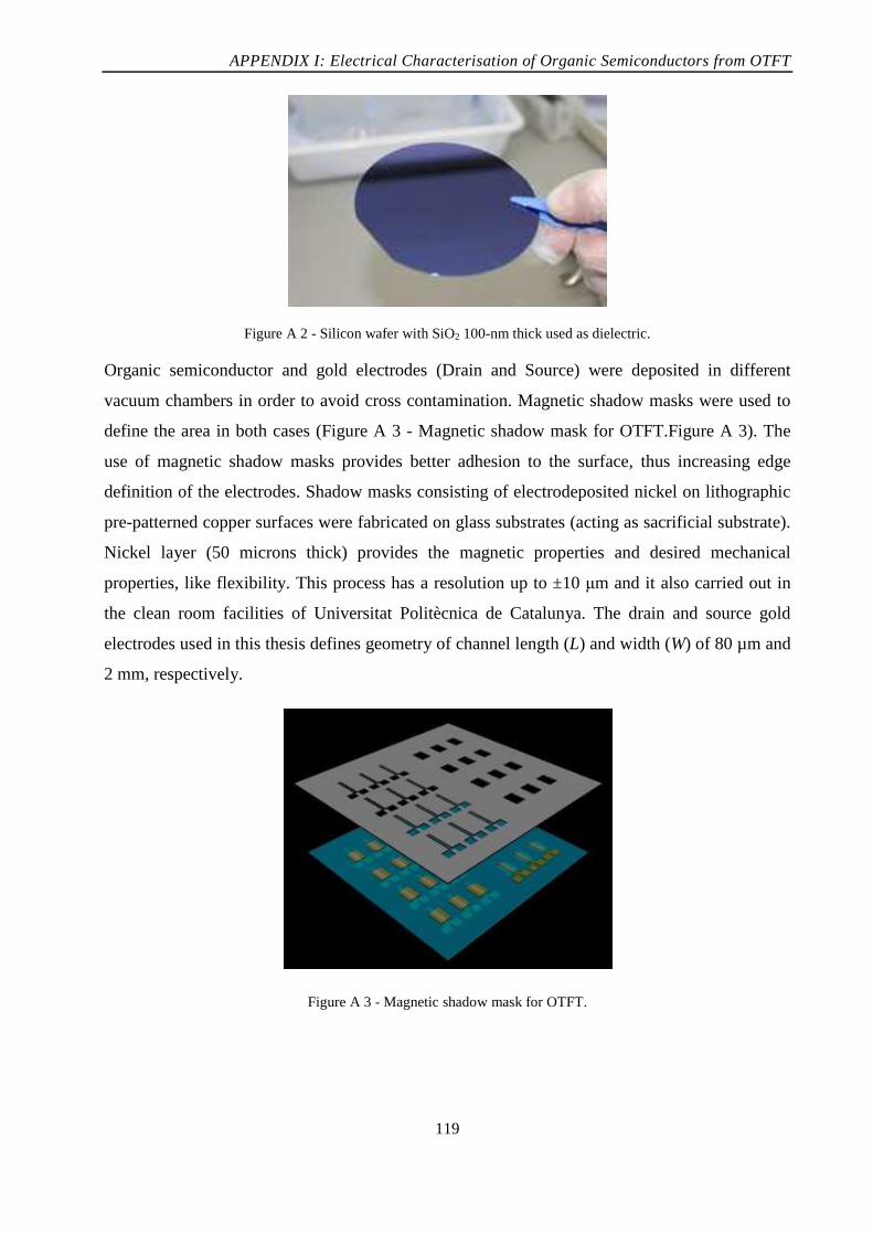
APPENDIX I: Electrical Characterisation of Organic Semiconductors from OTFT
119
Figure A 2 - Silicon wafer with SiO2 100-nm thick used as dielectric.
Organic semiconductor and gold electrodes (Drain and Source) were deposited in different
vacuum chambers in order to avoid cross contamination. Magnetic shadow masks were used to
define the area in both cases (Figure A 3 - Magnetic shadow mask for OTFT.Figure A 3). The
use of magnetic shadow masks provides better adhesion to the surface, thus increasing edge
definition of the electrodes. Shadow masks consisting of electrodeposited nickel on lithographic
pre-patterned copper surfaces were fabricated on glass substrates (acting as sacrificial substrate).
Nickel layer (50 microns thick) provides the magnetic properties and desired mechanical
properties, like flexibility. This process has a resolution up to ±10 μm and it also carried out in
the clean room facilities of Universitat Politècnica de Catalunya. The drain and source gold
electrodes used in this thesis defines geometry of channel length (L) and width (W) of 80 µm and
2 mm, respectively.
Figure A 3 - Magnetic shadow mask for OTFT.

APPENDIX I: Electrical Characterisation of Organic Semiconductors from OTFT
120
A_I.3 Characterisation of OTFT
The fabricated OTFTs were characterised in the dark and under moderate vacuum conditions
(10-1 mbar) to minimise oxidation effects during the electrical characterisation process. The
electrical characteristics were measured using an Agilent 4156C parameter analyser. The device
temperature was varied from 300 to 390 K by means of an MMR Technologies controller (model
K–20).
A_I.3.1 Determination of Mobility μ
A brief review of different methods to determine the charge carrier mobility of organic
semiconductors can be found in Chapter 2, section 2.4. Here, it is detailed the methodology
followed in order to determine the mobility from electrical characterisation of OTFT.
The current between source and drain ISD depends on the mobility of the charge carriers μ,
geometry of device: channel length L and width W, capacitance of the oxide per unit area Cox,
gate voltage VG, source-drain voltage VSD, and the threshold voltage VTH which is required to
create the channel.
The following Eq. A.1 defines the drain-source current in the linear region for a Thin-Film
Transistor:
In saturation regime (VGS – VTH < VDS), the induced charge carriers limit the current between
source and drain, therefore IDS is constant independently of the increasing voltage between the
electrodes. The current flow depends only on VG and the parameters of the transistor. Applying
the condition (VGS – VTH = VDS) to Eq. A1, the ISD for this regime can be expressed as Eq. A2,
which depends quadratically on the gate voltage:
The mobility can be determined from equation Eq. A2 by plotting the square root of ISD versus
VG. Fitting a straight line to the square root of the measured drain current yields the field-effect
charge carrier mobility µ and the threshold voltage VT. Eq. A3 shows the steps to determine the
equation for the linear fit.
%'& ()XY# C*& +Z '&2 D '& (A.1)
%'& 12
(# )XY *& +Z (A.2)

APPENDIX I: Electrical Characterisation of Organic Semiconductors from OTFT
121
Using the expression of linear fit ([ \A ]) (Eq. A4):
Finally, the expressions to determinate the µ and VT are:
It is important to note that, as mentioned above, the mobility is not a constant parameter as it
depends on the VGS. Hence, the Eq. A5 is estimation and the obtained values must be treated as
such.
If VGS is equal to VDS we ensure that the device is in saturation regime. To carry out the
saturation characteristic, ISD is measured by a sweep of voltages (VGS = VDS) from very low
conduction to high conduction (|VGS | >> | VTH |). This measurement shows an exponential
characteristic as depicted in Figure A4.
-50 -40 -30 -20 -10 00,0
5,0x10⁻⁴
1,0x10⁻³
1,5x10⁻³
2,0x10⁻³
2,5x10⁻³
Gate Voltage (V)
y = Ax - B
sqr
t (Id
s (A
))
VTH
Figure A 4 - Linear fit in saturation measurement for p-type OTFT.
^%'& _12 ( # )XY *& − +Z = _ ( )XY2# *& − _ ( )XY2# +Z
(A.3)
\ = _ ( )XY2# ] = _ ( )XY2# +Z A = *& (A.4)
= \ ( )XY2# +Z = ]\ (A.5)

APPENDIX I: Electrical Characterisation of Organic Semiconductors from OTFT
122
A_I.3.2 Determination of Density of States (DOS)
The optoelectronic properties of the devices depend largely on the density of states (DOS) in the
band gap of the active semiconductor layers. DOS distribution in semiconductors determines the
electrical transport, photosensitivity, doping efficiency and, at the end, impairs the device
performance (traps and recombination centres). Figure A5 illustrates how the energy spectrum of
amorphous semiconductors differs from that of crystal semiconductors in the presence of density
“tails” of electronic states that penetrate the energy gap.
Figure A 5 - (left) Ideal semiconductor (Crystalline materials (silicon). Well defined valence & conduction bands.
No states in the middle of the gap. (right) Amorphous and polycrystalline semiconductors. States inside the gap.
Experimental information on the distribution of defects cannot be obtained in a straightforward
way. Different techniques for extracting information about the energy distribution of the DOS in
thin-film semiconductors: ultraviolet photoelectron spectroscopy, Kelvin probe force
microscopy, electron spin resonance spectroscopy, space-charge-limited-current spectroscopy,
deep-level spectroscopy, photoconductivity measurements [9–14].
In this thesis, we estimate the DOS distribution in organic semiconductor thin-films from
electrical measurements performed at different temperatures on OTFTs. This measurements will
provide information about the thermal emission energy distribution of trapped charges.
The multiple trapping and thermal release model (MTR) should describe charge transport in
disordered small-molecule organic semiconductors [15]. The trapping and release mechanisms
determines the overall mobility and the thermally activated behaviour. The trap distribution DOS
within the gap is believed to be exponentially shaped. Therefore, a crucial feature for the MTR
model is the determination of the DOS in the gap of the semiconductor.

APPENDIX I: Electrical Characterisation of Organic Semiconductors from OTFT
123
The position of the Fermi level provides extensive information about the electrical characteristics
of the semiconductor material, such as the density of trap states in the bandgap or the distribution
of states in the band tails.
It has been observed that the behaviour conductivity (σ) in thin-film organic semiconductors is
thermally activated, following the Arrhenius model (Eq A6):
where Ea is the activation energy, kB the Boltzmann constant, T the temperature in K and σ0 a
constant of the material. Ea can be considered a measure of the distance from the Fermi level
(EF) position to the transport band edge. In consequence, Ea is Ea = Ec - EF for n-type
semiconductors and Ea = EF - Ev for p-type.
On the other hand, from the experimental data obtained from the characterisation of OTFTs, the
conductivity can also be calculated from the IDS-VDS curve, as expressed in the following
expression (Eq A7):
Applying Eq A6 in Eq A7 can be obtained (Eq. A8):
Thus, if ISD is measured at two different temperatures with a fixed VGS = VDS, we obtain (Eq. A9):
From Eq A9, it can be easily extracted the value of Ea of the conductivity.
On the other hand, Fermi level position in the semiconductor can be varied with the VGS voltage.
When applying a VGS voltage, more charge is accumulated in the conductive channel of the Thin-
Film Transistor. For a n-type semiconductor applying a positive voltage in the gate will induce
more negative charge (electrons) to be accumulated in the channel, whereas the application of
positive VGS will empty the channel from electrons. Since the amount of charge accumulated in
the channel depends on the position of the Fermi level, changing VGS shifts the Fermi level
position inside the band-gap of the semiconductor. In the case of n-type semiconductor, a
` 1234a6b+8
(A. 6)
` ( # c %'&'& (A. 7)
%'& # c( '& 1234a6b +8 % 1234a6b +8 (A. 8)
ln%'&e ln%'&f C 0gh D C 0gh D 0gh C 1 − 1D (A. 9)

APPENDIX I: Electrical Characterisation of Organic Semiconductors from OTFT
124
positive VGS will shift the EF to the LUMO level (conduction band in the case of inorganic
semiconductors), whereas a negative EF will shift EF towards the middle of the gap (in an n-type
semiconductor EF lies close to LUMO level). A similar description can be made in the case of p-
type semiconductor. In this case, EF lies close to the HOMO level, and the application of a VGS
voltage will shift EF to the HOMO level for a negative VGS and to the middle of the band-gap for
a positive VGS.
The transfer characteristic of the device is necessary to be measured at different temperatures to
achieve Ea.
The transfer curve was measured several times by applying heating and cooling cycles until the
results were stable. Since the transfer characteristics are measured at a fixed VDS voltage, the
drain current is proportional to the channel conductance for each VGS voltage. An Arrhenius plot
of the channel conductance gives evidence of a thermally activated behaviour.
-30 -25 -20 -15 -10 -5 0 510
-12
10-11
10-10
10-9
10-8
300 K
310 K
320 K
330 K
340 K
350 K
360 K
370 K
I DS
(A)
VGS
(V)
Figure A 6 - Transfer characteristic of TFT measured from 300 K to 370 K with step of 10 K.

APPENDIX I: Electrical Characterisation of Organic Semiconductors from OTFT
125
2,7 2,8 2,9 3,0 3,1 3,2 3,3 3,410
-10
10-9
10-8
10-7
Vgs=-12.5V
Vgs=-16V
Vgs=-19.5V
Vgs=-23V
Vgs=-26.5V
Vgs=-30V
I DS
(A)
1000/T (1/K)
Figure A 7 - Arrhenius plot of drain-source current in function of temperature.
-30 -25 -20 -15 -100,2
0,4
0,6
0,8 R.T.
60ºC
90ºC
120ºC
Ea
(eV
)
VGS
Figure A 8 - Activation energy of TFTs, where the semiconductor layer were deposited at different substrate
temperature, in function of gate-source voltage.
The rate at which Ea varies with VGS indicates how easily the Fermi level can shift through the
DOS distribution in the gap of the organic semiconductor. A fast variation of Ea with VGS takes
place if a low density of localised states has to be filled by trapped carriers. In contrast, a high
DOS in the gap results in slower variations of Ea with VGS.
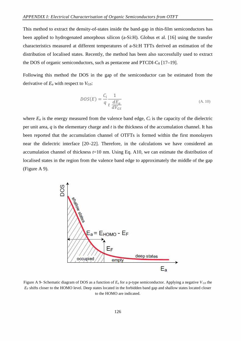
APPENDIX I: Electrical Characterisation of Organic Semiconductors from OTFT
126
This method to extract the density-of-states inside the band-gap in thin-film semiconductors has
been applied to hydrogenated amorphous silicon (a-Si:H). Globus et al. [16] using the transfer
characteristics measured at different temperatures of a-Si:H TFTs derived an estimation of the
distribution of localised states. Recently, the method has been also successfully used to extract
the DOS of organic semiconductors, such as pentacene and PTCDI-C8 [17–19].
Following this method the DOS in the gap of the semiconductor can be estimated from the
derivative of Ea with respect to VGS:
where Ea is the energy measured from the valence band edge, Ci is the capacity of the dielectric
per unit area, q is the elementary charge and t is the thickness of the accumulation channel. It has
been reported that the accumulation channel of OTFTs is formed within the first monolayers
near the dielectric interface [20–22]. Therefore, in the calculations we have considered an
accumulation channel of thickness t=10 nm. Using Eq. A10, we can estimate the distribution of
localised states in the region from the valence band edge to approximately the middle of the gap
(Figure A 9).
Figure A 9- Schematic diagram of DOS as a function of Ea for a p-type semiconductor. Applying a negative V GS the EF shifts closer to the HOMO level. Deep states located in the forbidden band gap and shallow states located closer
to the HOMO are indicated.
i0 ):; 1j 0g*&
(A. 10)

APPENDIX I: Electrical Characterisation of Organic Semiconductors from OTFT
127
References
[1] F. Ebisawa, T. Kurokawa, S. Nara, “Electrical properties of polyacetylene/polysiloxane interface”, J. Appl. Phys. 54 (1983) 3255.
[2] J. H. Burroughes, C. A. Jones, R. H. Friend, “New semiconductor device physics in polymer diodes and transistors”, Nature 335 (1988) 137.
[3] A. Tsumura, H. Fuchigami, H. Koezuka, “Field-effect transistor with a conducting polymer film” Synth. Met. 18 (1987) 699.
[4] H. Fuchigami, A. Tsumura, H. Koezuka, “Polythienylenevinylene thin-film transistor with high carrier mobility” Appl. Phys. Lett. 63 (1993) 1372.
[5] G. Horowitz, D. Fichou, X. Peng, Z. Xu, F. Garnier, “A field-effect transistor based on conjugated alpha-sexithienyl” Solid State Commun.72 (1989) 381.
[6] Y -Y. Lin, D. I. Gundlach, S. F. Nelson, T. N. Jackson, “Pentacene-based organic thin-film transistors” IEEE Trans. Electron Dev. 444 (1997) 1325.
[7] H. Sirringhaus, N. Tessler, R. H. Friend, “Integrated Optoelectronic Devices Based on Conjugated Polymers” Science 280 (1998) 1741.
[8] C.D. Dimitrakopoulos, P.R.L. Malenfantols “Organic thin film transistors for large area electronics”, Adv. Mater., 14 (2002) 99.
[9] T. Sueyoshi, H. Fukagawa, M. Ono, S. Kera, N. Ueno, “Low-density band-gap states in pentacene thin films probed with ultrahigh-sensitivity ultraviolet photoelectron spectroscopy” Appl. Phys. Lett. 95 (2009)183303.
[10] O. Tal, Y. Rosenwaks, Y. Preezant, N. Tessler, C. K. Chan, A. Kahn, “Direct Determination of the Hole Density of States in Undoped and Doped Amorphous Organic Films with High Lateral Resolution”, Phys. Rev. Lett. 95 (2005) 256405.
[11] H. Matsui, A. S. Mishchenko, T. Hasegawa, “Distribution of Localized States from Fine Analysis of Electron Spin Resonance Spectra in Organic Transistors”, Phys. Rev. Lett. 104 (2010) 056602.
[12] C. Krellner, S. Haas, C. Goldmann, K. P. Pernstich, D. J. Gundlach, B. Batlogg, “Density of bulk trap states in organic semiconductor crystals: Discrete levels induced by oxygen in rubrene”, Phys. Rev. B 75 (2007) 245115.
[13] V. Nádaždy, R. Durný, J. Puigdollers, C. Voz, S. Cheylan, K. Gmucová, “Experimental observation of oxygen-related defect state in pentacene thin films”, App. Phys. Lett. 90 (2007) 092112.
[14] D. V. Lang, X. Chi, T. Siegrist, A. M. Sergent, A. P. Ramirez, “Amorphouslike Density of Gap States in Single-Crystal Pentacene”, Phys. Rev. Lett. 93 (2004) 086802.
[15] G. Horowitz, M. E. Hajlaoui, R. Hajlaoui, “Temperature and gate voltage dependence of hole mobility in polycrystalline oligothiophene thin film transistors”, J. Appl. Phys. 87 (2000) 4456.

APPENDIX I: Electrical Characterisation of Organic Semiconductors from OTFT
128
[16] T. Globus, H. C. Slade, M. Shur, M. Hack, “Density of deep bandgap states in amorphous silicon from the temperature dependence of thin film transistor current”, MRS Proceedings 336 (1994) 823.
[17] S. Scheinert, K. P. Pernstich, B. Batlogg, G. Paasch, “Determination of trap distributions from current characteristics of pentacene field-effect transistors with surface modified gate oxide”, J. Appl. Phys. 102 (2007) 104503.
[18] J. Puigdollers, A. Marsal, S. Cheylan, C. Voz, R. Alcubilla, “Density-of-states in pentacene from the electrical characteristics of thin-film transistors”, Org. Electron., 11 (2010) 1333.
[19] M. R. Shijeesh, L. S. Vikas, M. K. Jayaraj, J. Puigdollers, “Degradation study and calculation of density-of-states in PTCDI–C8 channel layer from the electrical characteristics of thin-film transistors”, J. Appl. Phys., 116 (2014) 024507.
[20] A. R. Völkel, R. A. Street, D. Knipp, “Carrier transport and density of state distributions in pentacene transistors”, Phys. Rev. B, 66 (2002) 195336.
[21] A. Dodabalapur, L. Torsi, H. E. Katz, “Organic transistors: two-dimensional transport and improved electrical characteristics” Science 268 (1995) 270.
[22] G. Horowitz, “Organic thin film transistors: from theory to real devices” J. Mater. Res. 19 (2004) 1946.