silicon oxidation ece/che 4752: microelectronics processing laboratory gary s. may january 15, 2004
TRANSCRIPT

Silicon Oxidation
ECE/ChE 4752: Microelectronics ECE/ChE 4752: Microelectronics Processing LaboratoryProcessing Laboratory
Gary S. May
January 15, 2004

Outline
IntroductionIntroduction Deal/Grove (Kinetic) ModelDeal/Grove (Kinetic) Model Impurity RedistributionImpurity Redistribution Masking Properties of SiOMasking Properties of SiO22
Oxide QualityOxide Quality Oxide Thickness MeasurementOxide Thickness Measurement

Definition Process by which a layer of silicon dioxide (SiO2) is grown on a
silicon substrate Applied exclusively to Si, since GaAs, Ge, and other
semiconductors don’t form native oxides Uses:
1) implant/diffusion mask
2) surface passivation
3) isolation
4) key component of MOS structures
5) dielectric for multilevel interconnect

Reactions
Dry oxidation:
Si + O2 → SiO2 (better quality)
Wet oxidation:
Si + 2H2O → SiO2 + 2H2 (faster growth rate)

Silicon Consumption
During growth, 1 mole of SiO2 takes up more volume than 1 mole of Si
To grow an oxide layer of thickness d, a layer of Si of thickness 0.44d is consumed
Outline
IntroductionIntroduction Deal/Grove (Kinetic) ModelDeal/Grove (Kinetic) Model Impurity RedistributionImpurity Redistribution Masking Properties of SiOMasking Properties of SiO22
Oxide QualityOxide Quality Oxide Thickness MeasurementOxide Thickness Measurement

Model Assumptions
Temperature: 700 - 1300 oC
Pressure: 0.2 - 1.0 atm
SiO2 thickness: 0.03 - 2 m

Basic Diagram
Co = concentration of oxidizing species at oxide surface (cm-3)
Cs = concentration of oxidizing species at Si surface (cm-3)
d = oxide thickness
F’s = fluxes (cm-2s-1)
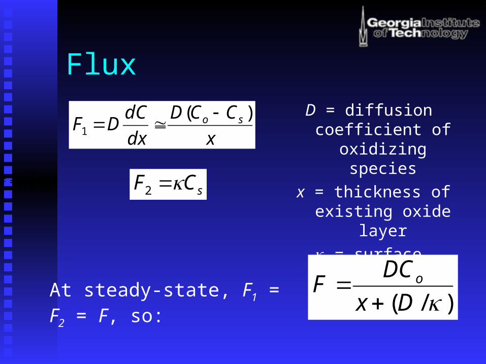
Flux
D = diffusion coefficient of oxidizing species
x = thickness of existing oxide layer
= surface reaction rate constant
x
CCD
dx
dCDF so )(
1
sCF 2)/(0
Dx
DCF
)/(0
Dx
DCF
)/(0
Dx
DCF
)/( Dx
DCF o
At steady-state, F1 = F2 = F, so:

Growth Rate
where:where:
CC11 = # molecules of oxidizing species/unit volume = # molecules of oxidizing species/unit volume
= 2.2 = 2.2 × 10× 102222 cm cm-3-3 for O for O22
= 4.4 = 4.4 × 10× 102222 cm cm-3-3 for H for H22OO
)/(
/ 1
1 Dx
CDC
C
F
dt
dx o
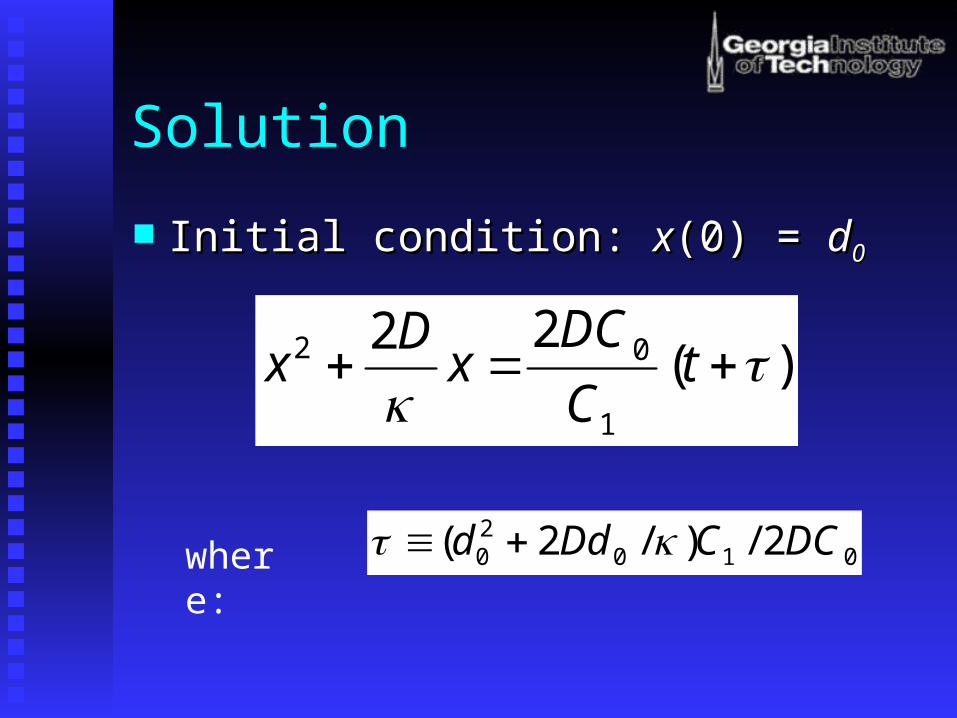
Solution
Initial condition: Initial condition: xx(0) = (0) = dd00
)(22
1
02
tC
DCx
Dx
where: 01020 2/)/2( DCCDdd
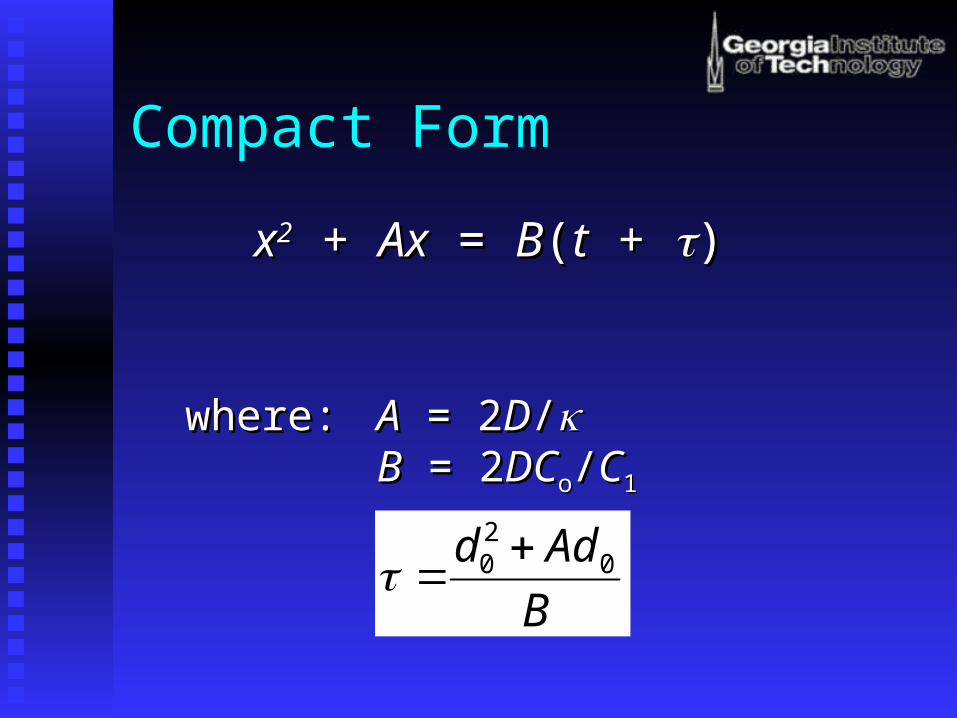
Compact Form
xx22 + + AxAx = = BB((tt + + ))
B
Add 020
where: where: AA = 2 = 2DD//BB = 2 = 2DCDCoo//CC11

Limiting Cases
Short times (reaction rate-limited):Short times (reaction rate-limited):
)( tA
Bx “Linear Regime”
Longer times (diffusion-limited):Longer times (diffusion-limited):
xx22 = = BB((tt + + ) ) “Parabolic Regime”“Parabolic Regime”

Thin, Dry Oxides
For wet oxidation, initial oxide thickness For wet oxidation, initial oxide thickness dd00
is very small (or is very small (or ≈≈ 0). 0). For dry oxidation, extrapolated value of For dry oxidation, extrapolated value of dd00
at at tt = 0 is about 25 nm. = 0 is about 25 nm. Thus, dry oxidation on bare silicon requires Thus, dry oxidation on bare silicon requires
a value for a value for that can be generated using that can be generated using this initial thickness. this initial thickness.

ExampleA silicon sample is oxidized in dry OA silicon sample is oxidized in dry O22 at 1200 at 1200 ooC for C for one hour. (a) What is the thickness of the oxide grown? one hour. (a) What is the thickness of the oxide grown?
SOLUTIONSOLUTION:: From Table 3-2, for dry O From Table 3-2, for dry O22 @ 1200 @ 1200 ooCC
AA = 0.04 = 0.04 m, m, BB = 0.045 = 0.045 mm22/h, /h, = 0.027 h = 0.027 h
Using these parameters, we obtain an oxide thickness Using these parameters, we obtain an oxide thickness of of
xx = 0.196 = 0.196 mm

Example (cont.)(b) How much additional time is required to grow 0.1 (b) How much additional time is required to grow 0.1 m m more oxide in wet Omore oxide in wet O22 at 1200 at 1200 ooC? C?
SOLUTIONSOLUTION:: From Table 3-1, for wet O From Table 3-1, for wet O22 at 1200 at 1200 ooC areC are
AA = 0.05 = 0.05 m, m, BB = 0.72 = 0.72 mm22/H/H
Since Since dd00 = 0.196 = 0.196 m from the first step, m from the first step,
= 0.067 h= 0.067 h
The final desired thickness is The final desired thickness is xx = = dd00 + 0.1 + 0.1 m = 0.296 m = 0.296 m. m. Using these parameters, we obtain an additional time of Using these parameters, we obtain an additional time of
tt = 0.76 h = 4.53 min = 0.76 h = 4.53 min
B
Add 020

Temperature Variation

Outline
IntroductionIntroduction Deal/Grove (Kinetic) ModelDeal/Grove (Kinetic) Model Impurity RedistributionImpurity Redistribution Masking Properties of SiOMasking Properties of SiO22
Oxide QualityOxide Quality Oxide Thickness MeasurementOxide Thickness Measurement

Segregation Coefficient
When two solids come together, an impurity in one will redistribute until it reaches equilibrium.
The ratio of equilibrium concentration of the The ratio of equilibrium concentration of the impurity in Si to that in SiOimpurity in Si to that in SiO22 is: is:
2SiOin impurity ofion concentrat mequilibriu
siliconin impurity ofion concentrat mequilibriuk

4 Cases of Redistribution

Outline
IntroductionIntroduction Deal/Grove (Kinetic) ModelDeal/Grove (Kinetic) Model Impurity RedistributionImpurity Redistribution Masking Properties of SiOMasking Properties of SiO22
Oxide QualityOxide Quality Oxide Thickness MeasurementOxide Thickness Measurement

Oxides as Dopant Masks SiO2 can provide a selective mask against
diffusion at high temperatures. Oxides used for masking are ~ 0.5-1 m thick.
DopantsDopants Diffusion Constants at 1100 Diffusion Constants at 1100 ooC (cmC (cm22/s)/s)
BB 3.4 3.4 × 10× 10-17-17 – 2.0 × 10 – 2.0 × 10⁻¹⁴-14
GaGa 5.3 5.3 × 10× 10-11-11
PP 2.9 2.9 × 10× 10-16-16 – 2.0 × 10 – 2.0 × 10⁻¹³-13
AsAs 1.2 1.2 × 10× 10-16-16 – 3.5 × 10 – 3.5 × 10⁻¹⁵-15
SbSb 9.9 9.9 × 10× 10-17-17

SiO2 Masks for B and P

Outline
IntroductionIntroduction Deal/Grove (Kinetic) ModelDeal/Grove (Kinetic) Model Impurity RedistributionImpurity Redistribution Masking Properties of SiOMasking Properties of SiO22
Oxide QualityOxide Quality Oxide Thickness MeasurementOxide Thickness Measurement

Dry vs. Wet Oxides
Wet oxides are usually used for masking SiO2 growth rate is much higher when water is
the oxidant. Dry oxidation results in a higher quality oxide
that is denser and has a higher breakdown voltage (5 – 10 MV/cm).
Thin gate oxides in MOS devices are usually formed using dry oxidation.

Oxide Charge Definitions
1. Interface trapped charge (Qit): located at Si/SiO2 interface
2. Fixed oxide charge (Qf): positive charge located within 3nm of Si/SiO2 interface
3. Oxide trapped charges (Qot): associated with defects in the SiO2
4. Mobile ionic charges (Qm): result from contamination from Na or other alkali ions

Oxide Charge Locations

Outline
IntroductionIntroduction Deal/Grove (Kinetic) ModelDeal/Grove (Kinetic) Model Impurity RedistributionImpurity Redistribution Masking Properties of SiOMasking Properties of SiO22
Oxide QualityOxide Quality Oxide Thickness MeasurementOxide Thickness Measurement

Color Chart
Thickness (Thickness (m)m) ColorColor
0.070.07 BrownBrown
0.310.31 BlueBlue
0.390.39 YellowYellow
0.410.41 Light orangeLight orange
0.470.47 VioletViolet
Not very accurate
Colors repeat periodically at higher thicknesses

Profilometry
Requires a step feature
Accurate for thicknesses in 100 nm – 0.5 m range

Ellipsometry
Polarization changes are a function of optical properties, thickness, and wavelength and angle of incidence of the light beam.
Differences in polarization measured by an ellipsometer, and oxide thickness can be calculated.
Polarization changes occur when light is reflected from or transmitted through a medium.