reviews - tinhoahoc.com · and no major effort is needed to develop new resist materi-als. as a...
TRANSCRIPT
Nanolithography
Recent Developments in Nanofabrication Using IonProjection LithographyAmpere A. Tseng*
From the Contents
1. Introduction.............595
2. Ions and Interactions................................596
3. IPL Systems.............599
4. Projection Masks andResists.....................601
5. Nanostructures Printedby IPL.......................604
6. Conclusions andOutlook.................... 606
Keywords:· ion sources· nanofabrication· nanolithography· nanostructures· resists
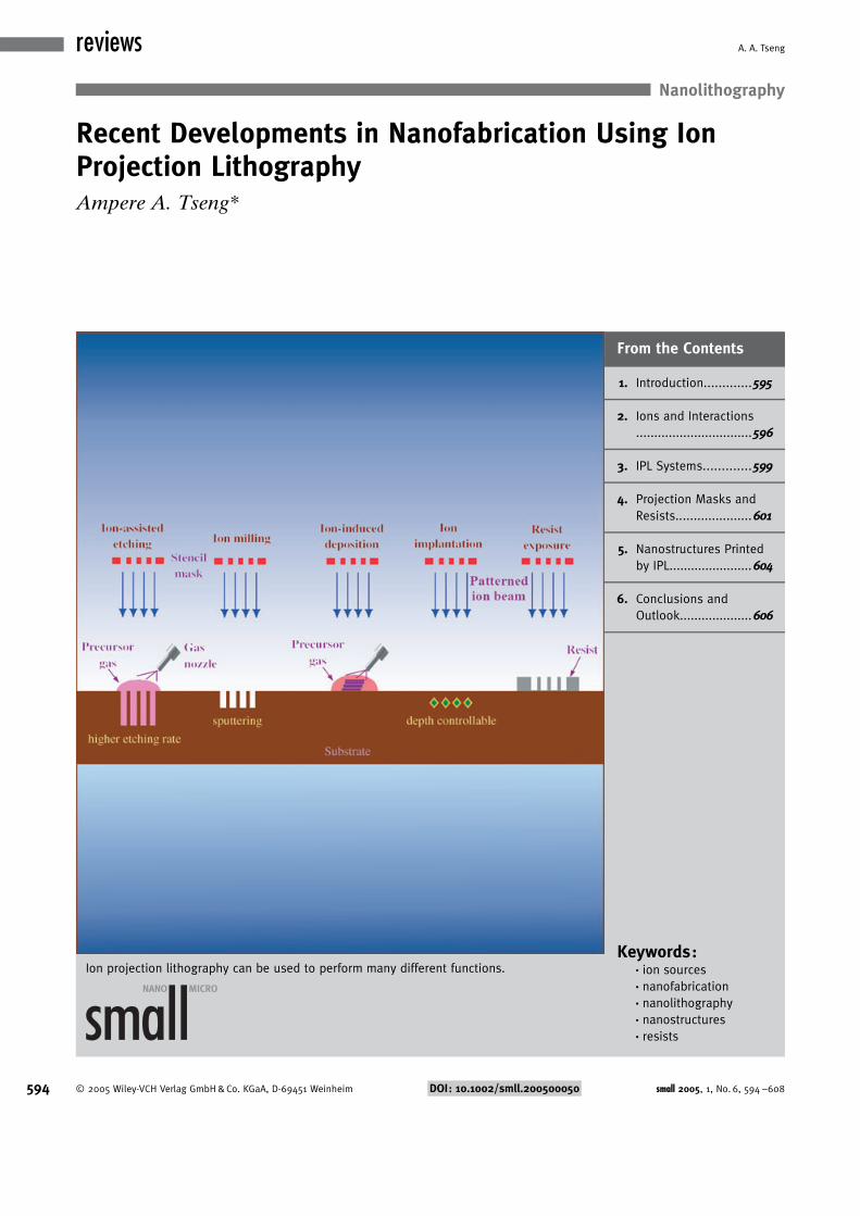
Ion projection lithography can be used to perform many different functions.
594 � 2005 Wiley-VCH Verlag GmbH & Co. KGaA, D-69451 Weinheim DOI: 10.1002/smll.200500050 small 2005, 1, No. 6, 594 –608
reviews A. A. Tseng

Ion projection lithography (IPL) is an emerging technology and a majorcandidate for the next-generation lithography (NGL) designed to comple-ment and supplement current optical lithographic techniques for future chipmanufacturing. In this Review, the recent developments of IPL technologyare examined with an emphasis on its ability to fabricate a wide variety ofnanostructures for the semiconductor industry. Following an introduction ofthe uniqueness and strength of the technology, the basics of ion-sourcedevelopment and ion–target interactions with and without chemicalenhancement are presented. The developments in equipment systems, masks,and resists are subsequently studied. The resolution of printed nanostructuresand the corresponding throughput of the current system are assessed forNGL. Finally, concluding remarks are presented to summarize the strengthsand weaknesses of the current technology and to suggest the scope for futureimprovement.
1. Introduction
In ion projection lithography (IPL), ions that are ex-tracted from a source and collimated through a mask withthe imaging pattern are accelerated through a series of elec-trostatic lenses that project the ions onto a wafer substrate,where the ions penetrate and modify the substrate materials.While passing through the lens system, the ions are acceler-ated from between tens of keV to hundreds of keV andthus, IPL can perform many different functions includingresist exposure, direct material sputtering, and the initiationof chemical reactions for etching or deposition (as indicatedin the frontispiece). In performing its major task, resist ex-posure, IPL is very similar to optical lithography (OL).Both use reduction optics to project an image onto thewafer, and stepping and repeating exposures are similarlyperformed with the use of a precisely controlled laser inter-ferometer stage.
Basically, IPL has the capability to realize printed fea-tures at 50 nm resolution by using lightweight ions toexpose a resist. A wide range of projection energy and ionspecies can be tailored to meet proper exposure or modifi-cation conditions of the material while at the same timecausing no damage to the underlying materials or circui-tries.[1, 2] IPL also has a large depth of focus (up to�500 mm) and very short exposure times (less than 0.5 s). Avariety of materials have been shown to work well with IPLand no major effort is needed to develop new resist materi-als. As a result, IPL has been selected as a major candidatefor next-generation lithography (NGL). NGL refers to thepost-optical lithography era and is designed to complementand supplement OL for future semiconductor manufactur-ing.
In addition to IPL, the candidates for NGL include ex-treme ultraviolet (EUV) lithography, electron projectionlithography (EPL), direct-write e-beam lithography (EBL),and X-ray lithography (XRL). Also, imprinting lithography(IL) was added as an NGL candidate in the 2003 edition of
the International Technology Roadmap for Semiconductors(ITRS) by SEMATECH.[3] Based on the current trend toproduce ever-shrinking device sizes and increased processorspeeds, it is expected that OL will become inadequate formaking some critical elements by the end of this decade.This is when NGL technologies should take over productionof these critical elements for state-of-the-art semiconductordevices. It is also expected that even after NGL becomesmature, OL will still be around and perform noncritical fea-tures. As such, NGL would coexist with OL for many moreyears and should be seamlessly implemented into the manu-facturing lines built for OL.
Since the worldwide market for semiconductor productsis huge (US$ 166 billion in 2003 according to the Semicon-ductor Industry Association), NGL technologies are allcompeting for a share of the next paradigm shift in lithogra-phy techniques. All of these technologies also have theirown particular weaknesses. IPL certainly is not perfect, butit offers several advantages for semiconductor manufactur-ers. For example, XRL is too expensive and has a shorterlifetime than IPL. The e-beam technology is too slow andhas far more potential for pitfalls than IPL. The optics forEUV are still problematic and have a relatively shorter life-time than IPL. It is inevitable that all these NGL technolo-gies have to make room for an alternative and complemen-tary technology such as IPL.[4]
A shift by the semiconductor industry to any NGL tech-nology would require the introduction of a new infrastruc-ture of tools, materials, and processing techniques, the re-
[*] A. A. TsengDepartment of Mechanical and Aerospace EngineeringArizona State University, Tempe, AZ 85287-6106 (USA)Fax: (+1) 480-965-1384E-mail: [email protected]
small 2005, 1, No. 6, 594 –608 DOI: 10.1002/smll.200500050 � 2005 Wiley-VCH Verlag GmbH & Co. KGaA, D-69451 Weinheim 595
Ion Projection Lithography

search and development costs of which would be enormous.A review article on IPL should provide the necessary infor-mation for making a good judgment in the selection of aNGL technique. As a result, the purpose of this Review isto assess the technical capabilities of IPL through an over-view of its recent technical advances, especially the strengthand weakness of the lithographic equipment already devel-oped, as well as the resolution of the nanostructures madeby the equipment. The ability to make a high-resolutionstructure is the most important and basic criteria in judgingthe suitability of NGL. At the present stage, to be competi-tive, any vital NGL candidate should have the ability tomake nanoscale structures. Here, a nanoscale structure ornanostructure can act as a component, device, or system,having a feature size in the range from 0.1 to 100 nm.
In this Review, the current developments in the litho-graphic capabilities of IPL, including ion sources, equip-ment, masks, and resists are first assessed. To illustrate theversatility and advancement of these lithographic capabili-ties, a wide variety of nanostructures made by different ex-posures and trial conditions are subsequently examined withan emphasis on the resulted resolution and equipmentthroughput. Finally, a summary of the current progress andthe scope recommended for future developments are pro-vided to conclude the present study.
2. Ions and Interactions
Ions are particles with net electrical charges, which usu-ally are atoms lacking one or more orbiting electrons.Therefore, they can be steered by electric or magneticfields. In IPL, ions are collimated into a beam that passesthrough a stencil mask and is projected onto the substrateusing electromagnetic lens systems. In this section, the char-acteristics and sources of ions as well as their interactionswith other materials and chemicals are discussed and ana-lyzed.
2.1. Characteristics of Ions
One of the most important features of IPL is that itsions have extremely small particle wavelengths (for in-stance, the de Broglie wavelength of 100 keV He+ ions isjust 5� 10�5 nm), whereas photon-based OL or EUV lithog-raphy is operated at the diffraction-limited resolution atwhich the shortest wavelength currently considered is onthe order of 10 nm in the EUV region. Certainly, charged-particle- (including ion-) based optical resolution is limitedby lens aberrations. In general, for particle-based optics, onerequires that the diffraction-limited resolution should beone tenth of the minimum feature size to be printed.
Moreover, ions possess advantages over other high-energy particles used in nanofabrication. For example, whencompared to electrons, ions are much heavier and can strikewith greater energy at relatively shorter wavelengths to di-rectly transfer patterns onto hard materials (such as semi-conductors, metals, or ceramics) without major forward- andback-scattering. Thus the feature size of the patterns islargely dictated by the beam size and the interaction of thebeam with the target material. On the other hand, electronsor photons can mainly be applied for writing on soft materi-als (such as polymers or resists) and the corresponding fea-ture sizes are determined by the proximity of the back-scat-tered electrons or wave diffraction limits. Moreover, the lat-eral exposure in an ion beam is very low, thereby exposingonly the correct areas and writing very narrow lines in thesubstrate, which makes it more capable to directly fabricatenanostructures.[5–7]
2.2. Ion Sources and Beam Quality
The ion source is important because its properties affectmany parameters involved in forming an ion beam as wellas the interaction between the beam and substrates in fabri-cation. Two major types of ion sources, point and volume-plasma sources, have been developed to produce nanome-ter-resolution patterns. Normally, point sources are used toform a focused ion beam (FIB), in which a sharp dot imageis focused directly on the substrate for direct writing. Onthe contrary, volume-plasma sources are used for IPL, inwhich a parallel ion beam is printed onto a substrate orresist through a mask with or without demagnification.
In general, the axial energy spread of the ion beamwhen coupled with the chromatic aberration in the ion opti-cal column can lead to blurring in the printed pattern on thetarget. Recently, the multicusp volume-plasma source hasreplaced the duoplasmatron volume source for ion-projec-tion printing because of its ability to provide a lower axial-energy spread of ions, which results in minimizing the chro-matic aberration of the projected image. Also, the multicuspsource can be used to produce large volumes of uniform,quiescent, and high-density plasmas with high gas and elec-trical efficiencies. The multicusp source is based on elec-tron-impact ionization, in which the energy transferred to agas molecule from an energetic electron exceeds the ioniza-tion energy by means of ionizing collisions. The electrons
Ampere A. Tseng is a Professor at Arizo-na State University. He received his PhDin mechanical engineering from the Geor-gia Institute of Technology in 1978, andhas published more than 200 peer-reviewed articles, edited more than tentechnical books, and is the holder of tenUS patents. He was a recipient of the Su-perior Performance Award and ASU Fac-ulty Award (1999–2000). He chaired theASME Materials Division in 1991–92 andwas elected as an ASME Fellow in 1995.He also chaired the NSF Workshop on
Manufacturing MEMS (2000) and co-chaired the International Confer-ence of Transport Phenomena in Processing (1992) and the USA–China Workshop on Advanced Machine Tool Research (1999).
596 � 2005 Wiley-VCH Verlag GmbH & Co. KGaA, D-69451 Weinheim www.small-journal.com small 2005, 1, No. 6, 594 –608
reviews A. A. Tseng

are energized through a gaseous discharge. Both the elec-trons and excited ions are accelerated by a dc field or rfpower at a frequency of a few MHz (up to 13.56 MHz) andare confined by an imposed magnetic field. The multicuspsource is generally used to produce hydrogen and heliumion beams. Other ion beams of Ne, Ar, and Xe can also begenerated.
Figure 1 shows a schematic of a filament-discharge mul-ticusp ion source. The external surface of the source cham-ber is surrounded by columns of permanent magnets (suchas samarium–cobalt alloy magnets), which generate longitu-dinal line-cusp magnetic fields that can confine the primaryionizing electrons (plasma) efficiently. The magnets areplaced around the cylindrical chamber and on the flangeend, since an extraction system is frequently placed on theopposite (open) end. Such magnet placements result in anasymmetric distribution of the plasma potential inside thesource that is crucial in controlling the axial or longitudinalenergy spread.[8] The low-axial-energy ions are extractedfrom the open end of the chamber. Magnetic filters are usedto reflect the high-energy electrons so that ion productionoccurs mainly in the region between the tungsten filamentand the filter where there is high-density plasma and uni-form plasma potential. The extracted ion beam, therefore,exhibits a low axial-energy spread that can be lower than2 eV. On the other hand, the corresponding axial energyspread of a duoplasmatron ion source for a typical IPLsystem is in the range of 6 to 8 eV.[4]
Two current IPL systems are equipped with coaxial mul-ticusp ion sources: one is known as ALG-1000 built by aconsortium of industrial and research institutes in the USand Europe, the Advanced Lithography Group (ALG),while the other is the process development tool (PDT) sup-ported by an international IPL development program calledMEDEA. Using a specially designed extraction system, the
PDT, for example, can extract a 5 keV He+ beam to yieldan axial-energy spread of as low as 0.6 eV. Consequently,this ion source can be expected to produce sharp featuresand achieve the 50 nm resolution target.[9] The light ions(H+, H2
+ , H3+, He+) are particularly suitable for projection
printing because they have very little forward scattering andgive off very small energy to the secondary electrons in thepolymeric resist. More details of these two IPL tools will beelaborated later in Section 3.
Liquid-metal ion sources (LMISs) usually produceheavy and high-brightness ions that can be focused ontofine FIBs on the order of 10 nm with adequate current den-sities for direct writing. Normally, LMISs are not used forIPL and thus, are not elaborated here further. A good intro-duction on this subject can be found in other review arti-cles.[7, 10]
2.3. The Ion–Target Interaction
When an energetic ion collides with a target solid, it en-counters numerous elastic and inelastic collisions with theatoms and electrons in the solid, which leads to differentelectronic and atomic interactions. Depending on theamount of ion energy, many interaction events, such asbackscattering, sputtering, implantation, and nuclear reac-tion occur (as shown schematically in Figure 2). Some of theinteractions are not completely separable and may lead tounwanted side effects that need to be understood and avoid-ed for a specific application.
2.3.1. Elastic Interactions
If the incident ion is at a relatively low energy, it can bebackscattered by an atom or a group of atoms in the targetsolid through an energy or momentum exchange betweenthe ion and the atom (or atoms). The energy exchange orbackscattering can result in a deflection of the ion from theincident path to a new trajectory. Also, if the associated ion
Figure 1. Multicusp ion source for dc discharge using a hot tungstenfilament cathode with magnetic filters (courtesy of K. N. Leung ofLawrence Berkeley National Laboratory).
Figure 2. A schematic that shows the interactions that occur betweenions and a target solid.
small 2005, 1, No. 6, 594 –608 www.small-journal.com � 2005 Wiley-VCH Verlag GmbH & Co. KGaA, D-69451 Weinheim 597
Ion Projection Lithography

momentum is sufficiently large, an atomic dislocation canoccur, in which a surface atom in the solid lattice can be dis-lodged from a weakly bonded position to a more stronglybonded one. Ions with greater energies can cause internaldislocations in the bulk of the target solid.
If the energy (or momentum) of the incoming ion iseven higher, the collision can transfer enough momentum toentirely free one or more atoms, which are ejected from thesolid as a result. This interaction is called sputtering and isthe governing effect in an ion-milling process. The numberof atoms that are ejected is called the sputter yield and is ameasure of the efficiency of material removal. A small por-tion of these ejected atoms can leave as either positively ornegatively charged ions, which are also known as secondaryions, and can be used for material analysis as discussedlater. The yield is normally in the range of 1 to 50 atoms perion and is a function of many variables, including the massof the ion and target atom, ion energy, ion incident angle,target temperature, and ion flux. There is a threshold forsputtering to occur. At a point above the threshold, thesputtering yield rises to a maximum and eventually decreas-es at a relatively high energy as the ion penetrates into thesolid and cannot reach the surface (ion implantationoccurs). As a result, the proper energy for sputtering is be-tween 10 to 100 keV for most ion species used. Because thesputtering depends solely on momentum transfer to removethe atoms, it is a purely physical process and, therefore, isalso called physical ion etching.
As mentioned earlier, as the ion energy increases fur-ther, the ion penetrates into the solid and ion implantationoccurs. The ion loses energy to the atoms and electrons inthe solid and becomes trapped inside the lattice. The lostenergy can also cause the atoms or nuclei in the solid to bedisplaced from their normal lattice sites. The trapped ionsor replaced atoms can alter the properties of the solid. Thesemiconductor property change by doping is one of themost common examples of ion implantation. Normally, thedepth of penetration decreases as the ion mass or the soliddensity increases.
Most of the above-discussed interactions, including scat-tering, sputtering, and implantation, involve momentum (orenergy) exchange between the ion and the atom, and can bedescribed by two-body elastic collisions. This type of inter-action is often called an elastic interaction and can lead tothe displacement of lattice atoms, sputtering, and the forma-tion of defects.[11]
2.3.2. Inelastic Interactions
The incident ions also interact with the target�s elec-trons, which can lead to useful signals for material analyses.In general, the interactions of the ion with the electrons donot cause any appreciable scattering of the incident ion be-cause the momentum transfer is relatively small. However,the interactions create excitation and ionization of electronshells of both the incident and target atoms. If this excita-tion occurs near the surface, it results in the emission of sec-ondary particles (electrons and ions), optical photons, andcharacteristic X-rays. This type of interaction involves differ-
ent forms of energy or particles and is termed as an inelasticinteraction (as opposed to the elastic interactions describedearlier). The emission can be strong enough to be detectedwithout excessive noise and thus is used as a signal to createhigh-magnification images of the target solid.
The technique of detecting the low-energy secondaryelectrons and/or secondary ions to determine the morpholo-gy or chemical composition of the target solid is called scan-ning ion microscopy (SIM). SIM is very similar to scanningelectron microscopy (SEM). In both cases, charged particlesare focused onto the surface of the target and rasteredacross it. SIM does not enjoy the popularity of SEM be-cause the spot characteristics of ion beams are poorer thanthose of high-quality SEM. On the other hand, by supplyinga broad low-energy electron beam to neutralize the targetsor to eliminate the charge build-up, an SIM can be used forimaging a highly insulating target without a conducting sur-face coating, as would be required in an SEM.[10]
Furthermore, if the direction of the ion beam is alignedwith a plane or axis of a crystal, ions travel through the crys-tal with less energy loss (lower collision loss) and result in alower sputtering yield. This phenomenon is called channel-ing and has a profound effect on the secondary ion and elec-tron yields. It has also been used in the development ofmasks for IPL. By differentiating the secondary particleyields with and without channeling, SIM can provide strongcontrast images of crystallography for studying the local dif-ferences in a crystal. Also, SIM can supply more informa-tion about the chemical nature of the target surface, sincelow-energy electrons are sensitive to the work function ofthe surface. Similarly, SIM is also used for high-resolutionsurface analysis by detecting the secondary ions. Since themechanisms to create the secondary electrons and secon-dary ions are different, the contrast obtained from eachtechnique can provide much more information on the sur-face and amorphous characterizations.
The secondary ions can also be created by the incidentions through elastic nuclear collisions. The technique of de-tecting these secondary particles to provide different aspectsof the examined target solid is called secondary ion massspectroscopy (SIMS). Since the energy of a sputtered ion isrelatively low and its range is very short, SIMS is extremelysurface sensitive and provides real-time high-resolutionimages of the target material. Secondary ions originatingfrom elastic nuclear collisions are somewhat difficult to dis-tinguish from those created by inelastic atomic excitationand ionization. In fact, a typical SIMS probe uses the secon-dary ions generated by both elastic and inelastic interactionsto perform the analysis. Typically, the ion energy used forSIMS and SIM is in the range of tens of keV, where theemitted secondary electrons have an energy distributionpeak of a few eV and the secondary ions may have manykeV of energy. Since SIMS or SIM works by analyzing ma-terial removed from the target by sputtering, it can be con-veniently used in parallel with the FIB sputtering or millingprocesses. On the other hand, the fact that sputtering is adestructive process has also limited the applications ofSIMS and SIM. The resolution for a modern SIMS or SIMapparatus can be as small as 20 nm.[12]
598 � 2005 Wiley-VCH Verlag GmbH & Co. KGaA, D-69451 Weinheim www.small-journal.com small 2005, 1, No. 6, 594 –608
reviews A. A. Tseng

In higher-energy collisions between the ion and the elec-trons, an electron can be ejected from an inner shell. Subse-quently, the electrons in other shells rearrange themselveswith the emission of a quantum of energy (X-ray), which ischaracteristic of the target atom. This X-ray signal can beused to quantify the chemical composition of the targetsolid with high accuracy and sensitivity. Detection of theseX-rays can be accomplished by an energy- or a wavelength-dispersive spectrometer. For an ion energy increasing toMeV levels, interactions with a target solid can permit moreanalytical and imaging abilities. For example, techniquessuch as proton-induced X-ray emission (PIXE), proton-in-duced gamma-ray emission (PIGE), nuclear reaction analy-sis (NRA), and ionoluminescence have been developed touse the excited X-rays, excited g-rays, outgoing nuclear reac-tion particles, and visible and infrared emissions, from thetarget materials, respectively. Many of these techniques canbe combined with channeling to study the lattice location ofspecies (channeling contrast microscopy). The use of ionbeams for imaging or analyses is helpful, but is not directlyrelated to IPL. Consequently, this subject will not be dis-cussed any further.
At ultrahigh energies, normally much higher than1 MeV, nuclear reactions may occur and the ion can inflictlarge-scale damage to the target solid. Practically, this levelof ion energy is beyond the useful range for nanofabricationand will not be discussed here. Some recent developmentsin this subject, especially in heavy-ion reactions, may befound in the publication by Choudhury and Kicinska-Habior et al.[13, 14]
2.4. Chemical Reactions
In addition to elastic and inelastic interactions with thetarget substrate, the energy of incident ions in the presenceof a reactive gas can also lead to chemical reactions in theform of either ion-assisted etching (IAE) or ion-induceddeposition (IID).
In IAE, the ion beam causes the precursor gas to reactwith the substrate material to form volatile products thatcan be easily removed by the pump system at rates muchhigher than sputtering alone. To have a better control of theetched dimension, the precursor gas should not react withthe target substrate without the ion beam energy. The fre-quently used gases include halides (Br2, Cl2, I2, XeF2) foretching certain metals and insulators, and H2O for carbon-based materials.
In IID, the ion beam causes the molecules of the precur-sor gas to dissociate and leave the desired reaction productson the target surface or the outermost layer of the depositedstructure, while the volatile reaction products desorbedfrom the surface are removed through a vacuum pumpingsystem. The precursor gases for metal deposition are nor-mally organometallic. Insulators or polymeric materials canalso be deposited by different gas mixtures. Although IID isbased on a similar principle to that of chemical vapor depo-sition (CVD) used in the semiconductor industry, it has abetter resolution with a lower deposition rate, which is espe-
cially appropriate for nanofabrication. Since the incidentions simultaneously sputter the target, the ion energyis normally controlled at less than 30 keV; otherwise, thesputtering rate can significantly diminish the depositionrate.
Within the focus of this Review, ions with moderateenergy levels, typically in the range of 20 eV to 200 keV, arethe main interest because at this range, the ions can be ef-fectively used for IPL. The associated interactions, especial-ly sputtering, implantation, and ion-aided chemical reac-tions, will be discussed separately with a focus on their spe-cific fabrication techniques and nanoscale applications.
3. IPL Systems
In an IPL system, a collimated beam of ions passesthrough a mask and the ion beam is accelerated by an elec-trostatic lens to create a demagnified image of the mask onthe wafer. The wafer is stepped chip by chip. It is not diffi-cult for IPL to achieve the desired ion energy (�100 keV).In fact, most of the ion implanters currently used by thesemiconductor industry can deliver a small-scale collimatedbeam of ions at this energy level. However, in IPL, it is achallenge to deliver a big enough exposure area, especiallylarger than 1 cm2, at desirable energy levels with minimumenergy spreads (less than a few eV). Many efforts that havebeen devoted to the enhancement of the exposure or pro-jection area and other IPL-related technologies are dis-cussed below.
3.1. IPLM and ALPHA
The first practical IPL tool, called the ion projectionlithography machine (IPLM), was developed and hasevolved through the efforts of a group of scientists and engi-neers at Ionen Mikrofabrikations Systeme GmbH (IMS), inVienna, Austria. The IPLM-01 was the first prototypewhich, after being tuned up, became the IPLM-02 in 1988.This tool is still in use for performing research and proto-type testing; some results from this tool are described inSection 4. IPLM uses 5� or 10 � demagnifying ion-opticsfor the reduction printing of open stencil masks having asub-100 nm resolution, as reported by Stengl et al.[15]
Figure 3 shows the trajectories of ions through the IPLMsystem. Ions are extracted from a source resulting in a diver-gent ion beam, which illuminates the mask with an energyof about 5 keV. The extracted ions are H, He, N, Ne, Ar, orXe. The immersion lens accelerates the ions passing throughthe mask opening to a final energy of 60–90 keV or higher.The tool is equipped with a stable duoplasmatron ionsource enabling a current density of 10 mAcm�2. A prepro-jective lens octupole permits an electrostatic shift of the ionimage in the x and y directions, and a solenoid at this siteenables a rotation of the ion image through the action ofthe axial magnetic field. Furthermore, the scale of the pro-jected ion image can be adjusted electronically within plusor minus 3%. The IPL technique combines lithography with
small 2005, 1, No. 6, 594 –608 www.small-journal.com � 2005 Wiley-VCH Verlag GmbH & Co. KGaA, D-69451 Weinheim 599
Ion Projection Lithography

a direct sub-100 nm technique for ion-beam modification ofmaterials.[16]
The next tool developed by IMS was the ALPHA-10Xin 1990. This was an improvement over the IPLM-02 andwas horizontally built. In order to increase the useable fieldsize, the ALPHA machine reduction was changed from 10�to 5� , thereby increasing the field to 8� 8 mm2 in 1991.With the ALPHA-5X, a total distortion of 150 nm was real-ized. This was in perfect agreement with the IMS ion-opticalsimulations and calculations.[1] Efforts to develop these twoIPL tools by IMS demonstrated that IPL is a viable technol-ogy for future chip manufacture.
3.2. ALG
In 1992, the Advanced Lithography Group (ALG), aconsortium of industry and university institutes in the USand Europe, was formed with a goal to produce an IPL tool,ALG-1000, for projecting patterns in a stencil mask onto awafer substrate with a resolution less than 180 nm.[17–18] Toreach this goal, special low-distortion ion optics were devel-oped by IMS for exposing 20 � 20 mm2 fields at a 3� reduc-tion. The ion source adopted by ALG-1000, designed by theLawrence Berkeley National Laboratory (LBNL), is a 10-cm-diameter multicusp source, similar to that shown inFigure 1. The source can deliver a H+ or He+ beam with auseful beam current of 20 mA and an energy spread of lessthan 3 eV in order to limit the effect of chromatic aberra-tion to below 25 nm. The ALG system utilizes off-axis wafer
alignment, and a precision x–y stage controlled by a laser in-terferometer. The Einzel lens can project an ion image ofthe stencil mask onto the wafer substrate with better than2 mrad telecentricity. Demonstrated IPL performance hasshown less than 15 nm distortions over a 20 � 20 mm2 fieldand has indicated even larger fields being possible. Experi-ments have demonstrated that 100-nm-wide lines can be ob-tained in a Ray PN resist over an 8 �8 mm2 field by usingH+ ions at 55 keV. On the other hand, the same experimentwith a duoplasmatron source could only resolve 180-nm-wide lines.[16] At the end of the last century, through a con-tract with the US Defense Advanced Research ProjectsAgency (DARPA), the ALG-1000 was upgraded to ALG-1001 with all the necessary hardware and software as well asthe ancillaries to make the ALG a production-ready tooland was specifically used to demonstrate overlay registra-tion. Further refinement of the tool has been consideredsince.
3.3. PDT/MEDEA
In 1997, a new international consortium led by Infineonand Sematech, called MEDEA, was formed to build an IPLsystem known as the process development tool (PDT) fortesting the virtual source size, energy spread, homogeneity,total extract current, and lifetime of the source. Major ef-forts have been dedicated to build on the previous ALGwork and to implement a new multielectrode configurationto achieve a 50 nm resolution with an enhanced field sizeand a reduced column length.[19] A 4� reduction ion opticssystem has been developed for PDT, in which a printingarea of 12.5 �12.5 mm2 is designed to be patterned on to thewafer. To obtain a full image of the whole wafer area, eachprinting area is stitched one-by-one via synchronization ofthe beam and wafer moments.[20] The coaxial multicusp ionsource used in PDT is also developed by LBNL, and has avery low energy spread at 1 eV FWHM (full-width at half-maximum) level. Multielectrode electrostatic-ion-optics hasbeen used as the diverging electrostatic lens while an onlinediagnostic system and field-composable lens are used tocompensate for mechanical manufacturing inaccuracies.
The PDT is the most recent tool developed by IMS.Both the PDT and ALG technologies can be categorized assecond-generation IPL systems. As shown in Figure 4, themulticusp ion source of the PDT is equipped with a coaxialWien (ExB) mass filter and passes through a multielectrodeelectrostatic ion-optics stage to condense the ions into anearly telecentric ion beam of 115 mm in diameter (currentsize in PDT technology) to illuminate the stencil mask.[43]
After passing through the stencil mask, the ion beamlets arefurther accelerated to energies in the 70–150 keV range, andthen demagnified into a parallel beam whose image is fo-cused at the wafer. Meanwhile, a pattern lock system moni-tors the positions of 12 reference beamlets as they travelthrough the ion-optical system. Diagnostic elements are pro-vided to measure the energy spread, beam uniformity, anddistortion. The uniformity of the current density can be con-trolled within 3% of the current PDT system. By system op-
Figure 3. A schematic representation of the IPLM-2 lithographicsystem.
600 � 2005 Wiley-VCH Verlag GmbH & Co. KGaA, D-69451 Weinheim www.small-journal.com small 2005, 1, No. 6, 594 –608
reviews A. A. Tseng

timization, it is expected that the uniformity can be ach-ieved within 1%.
3.4. MMRL
Maskless or multibeam designs have also been consid-ered for IPL. Ando and Muray[21] did a preliminary study ofa multibeam IPL system, in which the multiple beams arecreated by a screen lens. The screen lens consists of an arrayof holes in a planar metal electrode and is used in conjunc-tion with a single-object aperture, which is illuminated by asingle ion beam. This object aperture is then demagnifiedby every hole in the screen lens, simultaneously formingmultiple images of the object. However, all beamlets haveto be deflected and blanked in synchronism and only onepattern can be written by a single beamlet. Later, Berryet al.[22] proposed a maskless system that uses an ion beamto illuminate a “blanking aperture array” and 200 � reduc-tion optics to expose the wafer in a scanning mode. Thisconcept offers the advantage of using a single source and ofrealizing a 25 nm spot size at the wafer with 5� 5 mm2 aper-ture dimensions. There are no mobile parts in the optics,that is, the only moving part in the system is a high-speedwafer stage.
By implementing the above multibeam and masklessconcepts with some modifications, LBNL has developed amaskless IPL system, which is known as maskless microion-beam reduction lithography (MMRL), as shown in Figure 5.As reported by Ngo et al.,[23] MMRL consists of a coaxialmulticusp ion source, a multibeamlet pattern generator, andan all-electrostatic accelerator column. The pattern genera-tor is used to create a lithographic pattern to eliminate theneed for masks. During processing, each individual ion
beamlet can be switched on or off to form the lithographicpattern by biasing the extraction electrode with respect tothe plasma electrode. Removing the use of stencil masksand the first stage, which is normally required by the otherIPL systems (such as ALG and PDT), can eliminate thecosts and efforts for mask development and fabrication, aswell as providing great potential for reducing the equipmentand operation costs. Jiang et al.[24] and Ngo et al.[23] haveused nine 50 mm switchable apertures to generate beamletswith 10� reduction ion optics to demonstrate the proof-of-concept of MMRL, and concluded that the maskless systemis a vital candidate for NGL.
However, the resolution of the pattern generated shouldbe dictated by the number of beamlets. The ability to havea large number of beamlets is a major challenge for MMRLand a high-resolution image on the substrate is essential forthe success of MMRL. No nano- or microscale structureshave been directly printed by the pattern using the multiplebeamlets. It is expected that a technology similar to the vari-able-shaped beam used in EBL will be developed forMMRL. In the variable-shaped beam technique, a reasona-ble number (initially, 36 to 64) of parallel ion beamlets havethe ability to form several types of primitive shapes (mainlyrectangles), and in every shot, only one of the shapes will beprojected on the substrate with a certain level (8 to 10times) of demagnification.[25] These primitive shapes aremuch smaller than the field sizes achieved in IPL. Thus, afew dozens of projected primitive shapes can then be stitch-ed into the final pattern, equivalent to the field size (1 to2 cm2) in IPL. More complex shapes can also be achievedby splitting the rectangles before the exposure. MMRL in-corporated with a variable-shaped beam system should be amore reasonable goal than developing a universal generatorfor the whole pattern in one shot. In this way, the shaped-beam system can increase the resolution by compromisingthe throughput achieved by the IPL system.
4. Projection Masks and Resists
The main challenge in IPL has been the projection maskbecause the absorption or transmission of ions is not similarto that of photons, in which the absorption or transmission
Figure 5. A schematic representation of the MMRL system, whichuses a universal pattern generator to form a lithographic pattern(courtesy of K. N. Leung of Lawrence Berkeley National Laboratory).
Figure 4. A schematic representation of the PDT/MEDEA lithographicsystem.
small 2005, 1, No. 6, 594 –608 www.small-journal.com � 2005 Wiley-VCH Verlag GmbH & Co. KGaA, D-69451 Weinheim 601
Ion Projection Lithography

is determined by the band structure of the mask materials.Most materials, including the least dense resists, can highlyabsorb ions and cause scattering of an incident ion beam, asdiscussed earlier in Section 2.3. In fact, a collimated ionbeam passing through a thin film or mask can emerge bothdiminished in number and in energy, and to some extent un-collimated. However, the difference in the energy loss ratein various materials is on the order of two, much smallerthan that of the particles in X-ray or UV technologies.Therefore, the concept of using material difference for alter-nate areas of absorbing and transmitting is difficult for ap-plications with IPL masks.
4.1. Stencil Masks
Most of the IPL systems use open stencil masks for pat-tern transformation as indicated by many investigators.[5, 6,20]
In the stencil mask, patterns are etched on the metal foils.This type of mask has excellent contrast because the ionsare not affected by passing through the open hole beforestriking on the resist. However, not all of the features canbe designed on a single stencil mask. A circle with middlefallout is a good example. Since there is no sublayer to holdthe etched middle fallout, every feature in the etched pat-tern has to be connected to each other and no island or de-tached sections can be included in the pattern. This is alsoknown as the “doughnut problem”.
To cope with the geometric restriction in stencil masks,the detached features can be patterned on as split or com-plementary features, and it is the sum of these that producesthe final intended features. In such an approach, the use ofa “split” mass (two parts of the same device located on thesame mask: an “A/B mask”) or a complimentary mask (twoor more separate masks, each containing a part of thedevice to be fabricated: “A + B masks”) is required. Eachof these techniques may also be used for layers that haveextremely long runs of lines from one side of the device tothe other. These layers can be split into what may look likedashed or segmented lines on one or each mask. Whenprinted, these lines are joined together to reform the wholeline pattern. A pattern lock system is then required to stitchor match these masks to print on the whole wafer.[1, 20]
Furthermore, in order to avoid the use of complementa-ry masks in disconnected geometries, continuous-membrane,single-crystal, channeling masks have been considered. Thechanneling mask benefits from the crystallographic channel-ing effect, that is, an increased range of ions incident alonga crystal symmetry axis, as discussed in Section 2.3.2. Parmaet al.[26] have studied a channeling mask that consists of asingle-crystal silicon membrane about 10 mm thick that hasbeen thinned to 0.6 mm, where transmission is desired. Theyfound that ions with an incident energy of 180 keV can dis-sipate more than 50 keV of energy passing through the 0.61-mm-thick Si and also create some scattering. Their findingslimit the resolution and the ultimate usefulness of the chan-neling mask, because the incident energy for most IPL sys-tems is relatively low (�10 kV) and the likely increase inangular spread and energy spread due to scattering is not
acceptable. Thus, further discussions will be limited to sten-cil masks.
4.2. Mask Fabrication
Single-crystal Si stencils appear to be popular because oftheir compatibility with the existing semiconductor process-es and good control of mask stress. Typically, the fabricationprocess consists of three major steps: membrane etching,membrane implanting and framing, and stencil pattern-ing.[27, 28] The membrane is fabricated by anisotropic wetetching from the back side of a wafer (normally 500 mmthick), typically using KOH as the etchant and SiO2 as theetching mask. A predefined p–n junction of 2 to 3 mm belowthe front surface is served as the etching stop. To preventwarping, the membrane is then prestressed by ion implanta-tion (or doping) to certain tensile stresses, typically 10MPa,which is somewhat lower than that of X-ray mask mem-branes. The membrane, with the perimeter of the originalwafer serving as a frame, is bonded to a thicker, machinedSi ring to ensure electrical conduction and thermal expan-sion compatibility. The oxide is then deposited on the frontside of the membrane and patterned by standard EBL andreactive-ion etching (RIE). The 2 to 3 mm-thick Si mem-brane is then etched in a Br2 RIE process with the oxideacting as an etching mask. This process yields reasonablygood vertical sidewalls. Frequently, the back of the mem-brane is coated with carbon to protect it from ion bombard-ment and to increase the emissivity. The above process issimilar to that of making piezoresistive pressure microsen-sors, except that the stencil mask can be as large as 200 mmand uses EBL for patterning.[29] A bonded stencil mask of150 mm in diameter is shown in Figure 6a. The stencil pat-
tern for structuring magnetic media is shown in Figure 6b,where the rectangular stencil openings are approximately320 nm wide and 2000 nm long. The corresponding struc-tures will be discussed in Section 5.2.
Recently, Letzkus et al.[30] developed a stencil mask witha thickness and diameter of 3 mm and 126 mm, respectively,for a PDT demonstration. They fabricated the mask on a sil-icon-on-insulator (SOI) wafer, in which the insulator layer isused as the etching stop, so that a predefined p–n junction isno longer required. Also, a deep RIE technique is adopted
Figure 6. Silicon stencil mask fabricated by EBL for the PDT system:a) The whole mask (150 mm in diameter); b) stencil pattern for aresolution test (after Loeschner et al.[33]).
602 � 2005 Wiley-VCH Verlag GmbH & Co. KGaA, D-69451 Weinheim www.small-journal.com small 2005, 1, No. 6, 594 –608
reviews A. A. Tseng
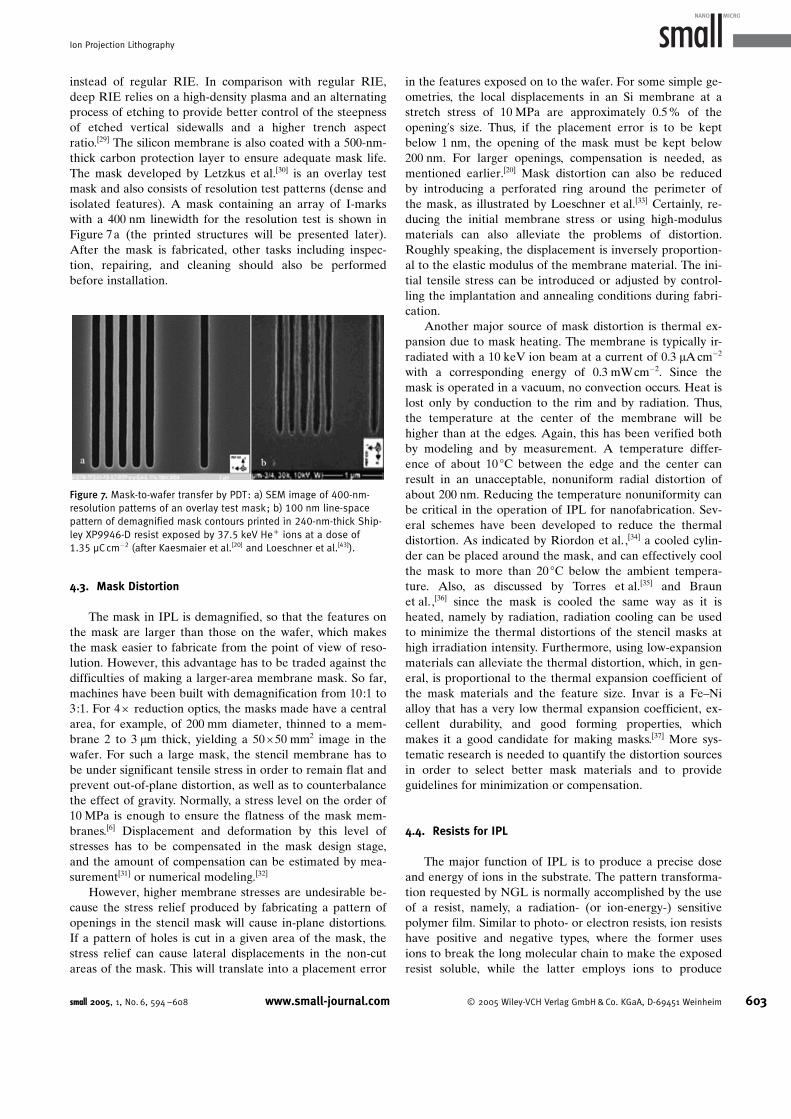
instead of regular RIE. In comparison with regular RIE,deep RIE relies on a high-density plasma and an alternatingprocess of etching to provide better control of the steepnessof etched vertical sidewalls and a higher trench aspectratio.[29] The silicon membrane is also coated with a 500-nm-thick carbon protection layer to ensure adequate mask life.The mask developed by Letzkus et al.[30] is an overlay testmask and also consists of resolution test patterns (dense andisolated features). A mask containing an array of I-markswith a 400 nm linewidth for the resolution test is shown inFigure 7a (the printed structures will be presented later).After the mask is fabricated, other tasks including inspec-tion, repairing, and cleaning should also be performedbefore installation.
4.3. Mask Distortion
The mask in IPL is demagnified, so that the features onthe mask are larger than those on the wafer, which makesthe mask easier to fabricate from the point of view of reso-lution. However, this advantage has to be traded against thedifficulties of making a larger-area membrane mask. So far,machines have been built with demagnification from 10:1 to3:1. For 4� reduction optics, the masks made have a centralarea, for example, of 200 mm diameter, thinned to a mem-brane 2 to 3 mm thick, yielding a 50 �50 mm2 image in thewafer. For such a large mask, the stencil membrane has tobe under significant tensile stress in order to remain flat andprevent out-of-plane distortion, as well as to counterbalancethe effect of gravity. Normally, a stress level on the order of10 MPa is enough to ensure the flatness of the mask mem-branes.[6] Displacement and deformation by this level ofstresses has to be compensated in the mask design stage,and the amount of compensation can be estimated by mea-surement[31] or numerical modeling.[32]
However, higher membrane stresses are undesirable be-cause the stress relief produced by fabricating a pattern ofopenings in the stencil mask will cause in-plane distortions.If a pattern of holes is cut in a given area of the mask, thestress relief can cause lateral displacements in the non-cutareas of the mask. This will translate into a placement error
in the features exposed on to the wafer. For some simple ge-ometries, the local displacements in an Si membrane at astretch stress of 10 MPa are approximately 0.5% of theopening’s size. Thus, if the placement error is to be keptbelow 1 nm, the opening of the mask must be kept below200 nm. For larger openings, compensation is needed, asmentioned earlier.[20] Mask distortion can also be reducedby introducing a perforated ring around the perimeter ofthe mask, as illustrated by Loeschner et al.[33] Certainly, re-ducing the initial membrane stress or using high-modulusmaterials can also alleviate the problems of distortion.Roughly speaking, the displacement is inversely proportion-al to the elastic modulus of the membrane material. The ini-tial tensile stress can be introduced or adjusted by control-ling the implantation and annealing conditions during fabri-cation.
Another major source of mask distortion is thermal ex-pansion due to mask heating. The membrane is typically ir-radiated with a 10 keV ion beam at a current of 0.3 mAcm�2
with a corresponding energy of 0.3 mW cm�2. Since themask is operated in a vacuum, no convection occurs. Heat islost only by conduction to the rim and by radiation. Thus,the temperature at the center of the membrane will behigher than at the edges. Again, this has been verified bothby modeling and by measurement. A temperature differ-ence of about 10 8C between the edge and the center canresult in an unacceptable, nonuniform radial distortion ofabout 200 nm. Reducing the temperature nonuniformity canbe critical in the operation of IPL for nanofabrication. Sev-eral schemes have been developed to reduce the thermaldistortion. As indicated by Riordon et al.,[34] a cooled cylin-der can be placed around the mask, and can effectively coolthe mask to more than 20 8C below the ambient tempera-ture. Also, as discussed by Torres et al.[35] and Braunet al.,[36] since the mask is cooled the same way as it isheated, namely by radiation, radiation cooling can be usedto minimize the thermal distortions of the stencil masks athigh irradiation intensity. Furthermore, using low-expansionmaterials can alleviate the thermal distortion, which, in gen-eral, is proportional to the thermal expansion coefficient ofthe mask materials and the feature size. Invar is a Fe–Nialloy that has a very low thermal expansion coefficient, ex-cellent durability, and good forming properties, whichmakes it a good candidate for making masks.[37] More sys-tematic research is needed to quantify the distortion sourcesin order to select better mask materials and to provideguidelines for minimization or compensation.
4.4. Resists for IPL
The major function of IPL is to produce a precise doseand energy of ions in the substrate. The pattern transforma-tion requested by NGL is normally accomplished by the useof a resist, namely, a radiation- (or ion-energy-) sensitivepolymer film. Similar to photo- or electron resists, ion resistshave positive and negative types, where the former usesions to break the long molecular chain to make the exposedresist soluble, while the latter employs ions to produce
Figure 7. Mask-to-wafer transfer by PDT: a) SEM image of 400-nm-resolution patterns of an overlay test mask; b) 100 nm line-spacepattern of demagnified mask contours printed in 240-nm-thick Ship-ley XP9946-D resist exposed by 37.5 keV He+ ions at a dose of1.35 mC cm�2 (after Kaesmaier et al.[20] and Loeschner et al.[43]).
small 2005, 1, No. 6, 594 –608 www.small-journal.com � 2005 Wiley-VCH Verlag GmbH & Co. KGaA, D-69451 Weinheim 603
Ion Projection Lithography

cross-linking between molecules to strengthen the exposedresist, thus making it more insoluble. The resist sensitivity isa measure of the minimum dose (in units of mC cm�2)needed to achieve these changes (e.g., a positive resist be-coming complete dissolved). The resist sensitivity using ionsis normally two orders of magnitude lower than that withelectrons. The main reason for this is that ions in the rangeof 1–200 keV lose most their energy in the resist (more pre-cisely, energy loss due to collisions with other particles, seeSection 2), while electrons in this range can penetratethrough the thin resist and lose a small fraction of theirenergy in the resist (because of their size, the collision fre-quency of electrons with other particles is much lower thanthat of ions). As a result, high-sensitivity resists are not re-quired, since the dose requirement to expose most organicresists is in the range from 5� 1011 to 3� 1013 ions cm�2 andthis range of ion energy can be relatively easy to obtain inIPL. In addition, by adjusting the ion energy, the penetra-tion depth can be conveniently matched to the desirable ex-posure depth of the resist. Thus, high-aspect-ratio structurescan be relatively easily fabricated.
Since a variety of resists are appropriate for IPL, nomajor efforts have been dedicated to develop new resist ma-terials. Poly(methyl methacrylate) (PMMA), G-line, I-Line,and deep-ultraviolet (DUV) resists with both positive andnegative tones work well with IPL.[20, 23] DUV chemical-am-plified resists (CARs) and PMMA are the two most populartypes of IPL resists and have the best combination of reso-lution, minor sensitivity, and etch resistivity. Other DUV re-sists appropriate for IPL include Hoechst�s AZ series, Olin�sHPR 506, and OCG�s HPR and ARCH.[6, 38] By applying thetop surface imaging (TSI) principle and using Ga ion-beamexposure associated with silylation and oxygen dry etching,a diazonaphthoquinone (DNQ)/novolak-based resist patterncan be obtained at a size as small as 30 nm while maintain-ing a high aspect ratio of up to 15, as indicated by Arshaket al.[39] It should be noted that the vacuum system used inIPL may cause outgassing of resists. More discussions onion resists can be found elsewhere.[38, 40, 41]
5. Nanostructures Printed by IPL
Two types of nanostructures can be printed by IPL. Thefirst type are polymeric resists used as the masks for thesubsequent etching or deposition for transferring patterns tothe underneath substrate, similar to the photoresist used inOL. The other uses IPL to directly sputter features in or de-posit features on to the substrate. Very often, the resist ma-terials can also be adopted as functional components and nosubsequent etching or deposition for pattern transferring isneeded. In this section, both the polymeric resists anddirect-printed structures are discussed.
5.1. Resist Patterning
For a resolution test, the stencil mask shown in Fig-ure 6b was used to expose a 50-nm-thick CARL resist using
a PDT with 45 keV He+ ions at a dose of 2.0 mC cm�2. TheCARL resist, developed by Infineon Technologies (Ger-many) for thin-film imaging, requires an exposure time of afew seconds.[40] As expected, through the 4� reduction ion-optics of PDT, the 320-nm-wide slots in the mask printedabout 80-nm-wide slot patterns in the resist, as shown inFigure 8a. In addition to this slot pattern, a pattern for aDRAM device test is also included in the same mask. Theprinted DRAM device image is shown in Figure 8b, and in-dicates that 60-nm-wide ribs and spaces can be obtained.Since both patterns are projected through a single mask,they can only be printed in the same resist at the same ex-posure conditions.[33]
The stencil mask fabricated on a SOI wafer shown inFigure 7a contains an array of overlay measurement marksand has been used for overlay tests. By a 4� reductionusing PDT, one of the overlay I-marks with a 400 nm line-width (Figure 7a) has been successfully used to print a 100-nm-wide I-mark pattern in a 240-nm-thick Shipley XP9946-D resist, as shown in Figure 7b.[20] A 37.5 keV He+ ionbeam at an exposure dose of 1.35 mC cm�2 is used to projectthe I-mark pattern onto this Shipley DUV chemical-ampli-fied resist, which exhibits a sensitivity of 0.8 mC cm�2 for37.5 keV He+ ions.[42] This result and the resolution testsshown in Figure 8a and b have demonstrated that mask-to-wafer transfer for isolated and arrayed lines/spaces can beperformed within the required accuracy. Also, as reportedby Loeschner et al. ,[43] some pattern collapse for 60 nmresist lines may be the limiting factor for determining the ul-timate resolution of IPL.
Moreover, exposures have been performed using theIPLM-02 ion projector on a Shipley UVII HS resist.[41] A3.5 keV He+-ion beam is used and accelerated behind themask to 75 keV. The resist used has been diluted so that athinner resist of 180-nm thickness can be obtained. For anH+-ion exposure of 75 keV, the resist sensitivity is1012 ions cm�2, which corresponds to 0.15 mC cm�2. An openstencil mask with arrayed patterns fabricated on a SOIwafer was used for a resolution study. Figure 9 a shows the
Figure 8. Exposure resolution test using 4 � PDT with 45 keV He+
ions at a dose of 2.0 mC cm�2: a) SEM image of a 80-nm-wide slotarray at a 150 nm period in 50-nm-thick Infineon CARL resist, usingthe stencil mask shown in Figure 6 b; b) SEM image of a DRAMdevice test pattern with 60 nm ribs in 230-nm-thick Infineon CARLresist (after Loeschner et al.[33]).
604 � 2005 Wiley-VCH Verlag GmbH & Co. KGaA, D-69451 Weinheim www.small-journal.com small 2005, 1, No. 6, 594 –608
reviews A. A. Tseng

stencil mask with a 650 nm linewidth, while through an 8.7demagnification by ion optics, a pattern of 75-nm-wide linesand spaces is printed on the DUV resist without a patterncollapse, as shown in Figure 9b. As indicated in Figure 9,
the mask shows good edge quality, while in the exposedresist, no proximity effect is visible at the line ends in theexposed resist pattern, even though the resist has been re-moved by a second exposure of equal dose to allow the sideview to be imaged by SEM. It is noteworthy that the higherdose used in the test can effectively reduce the edge rough-ness of the resist.
The IPLM-2 has also been used to assess the effect ofthe ion axial energy spread or beam quality on the printedstructures. The multicusp ion source shown in Figure 1 canbe equipped with a removable magnetic filter system, whichcan be used to provide a limited region of a transverse mag-netic field that prevents the energetic electrons in the dis-charge chamber from crossing over into the extractionregion. The plasma potential distribution in this case ismore uniform, and results in a narrowed axial energyspread of approximately 2 eV for a 10-cm-diameter by 10-cm-long filament discharge source.[8] Without the planarmagnetic filter system, the source in IPLM-2 is known tohave an energy spread of approximately 12 eV, which ismeasured using a retarding-field energy analyzer. Figure 10
shows the exposure results for a 390-nm-thick DUV resist(Shipley UVII HS) using 74 keV H+ ions with an exposuredose of 0.3 mC cm�2. At an 8.4 ion-optical reduction with anormal energy spread of 12 eV, the printed structure with a300 ms exposure time has a line space of 80 nm, as shown inFigure 10 a, while by using the planar magnetic filter (havingan energy spread of 2 eV), the corresponding line space orresolution improves to 50 nm with an exposure time of800 ms, as shown in Figure 10 b. The aspect ratio of theprinted line trench also increases from less than 3:1 to great-er than 4:1 with the magnetic filter. The study of Lee et al.[8]
demonstrates that the lower the energy spread, the betterthe resolution and higher the aspect ratio of the printedstructures.
5.2. Direct (Resistless) Printed Nanostructures
Ions have the unique feature of directly modifying awide range of materials without the need of a resist. In IPL,a whole surface area can be treated in parallel and can bepatterned into a substrate in a single-step process thatshould be much faster than the series process or direct writ-ing using FIB. IPL has been used for the resistless pattern-ing of semiconductors (Si, GaAs, poly-Si), insulating layers(SiO2, Si3N4), and metals (Al, Ni, Mo, Au) in addition topatterning organic thin films and resists. Under many condi-tions, it is desirable to avoid the use of a resist. For instance,while making high-temperature superconductor nanostruc-tures, undesirable chemical reactions can occur within theresist.
Brunger et al.[44] have used the IPLM-02 ion projector toperform direct milling on a 35-nm-thick Au film using anopen stencil mask with 8.7-demagnification ion optics. To in-crease the milling rate, the light ions normally provided bythe multicusp ion source used in IPLM-02 are replaced bythe heavier Xe+ species without any change in emission sta-bility or uniformity. Figure 11 a shows an array of line pat-terns milled with a dose of 2� 1015 Xe+ ions cm�2 at 75 keVhaving the smallest linewidth of 130 nm, while based on theprofile measurement by white light interferometry shown inFigure 11 b, the milling depth is 8 nm. The apparent rough-ness of the gold film is believed to be due to its grain struc-ture.
IPL milling should be especially attractive for fabricat-ing magnetic nanodots since other techniques, including OL,
Figure 10. Resist nanostructures printed by IPML-2 (for assessing theeffect of ion axial energy spread) using an ion source with a 12 eVaxial energy spread (left), and a 2 eV axial energy spread (right; afterLee et al.[8]).
Figure 11. IPL milling with 2 � 1015 Xe+ ions cm�2 at 75 keV in a poly-crystalline Au film: a) SEM image of a milled line pattern with a mini-mum width of 130 nm; b) surface-depth profile of the milled pattern(courtesy of W. H. Bruenger, Fraunhofer Institute, Berlin).
Figure 9. IPL resolution evaluation: a) SEM image of a stencil maskwith 650-nm-wide lines and spaces; b) SEM image of a 75 nm linepattern printed by 8.7 � reduction in 180-nm-thick Shipley DUVresist, exposed by 75 keV He+ ions at a dose of 0.46 mC cm�2
(courtesy of W. H. Bruenger, Fraunhofer Institute, Berlin).
small 2005, 1, No. 6, 594 –608 www.small-journal.com � 2005 Wiley-VCH Verlag GmbH & Co. KGaA, D-69451 Weinheim 605
Ion Projection Lithography

EBL, and IL, have to use resist-based processes that are notpreferable to keep the topography of a surface unchanged.This is extremely important for magnetic disks with a sur-face roughness of a few nanometers. Through a stencilmask, Dietzel et al.[45,46] used the IPLM-02 projector with a3 � 1014 Xe+ ionscm�2 dose at 73 keV to mill magnetic Co–Pt multilayers. Based on the magnetically altered areas mea-sured by magnetic force microscopy (MFM), Dietzelet al.[45] reported that magnetic islands with an average di-ameter of less than 100 nm are formed. Also, atomic forcemicroscopy (AFM) measurements indicated that the surfaceroughness of the topography after the IPL process is 1.1 nm(rms), which confirms that the topography change by IPL isnegligible. Thus, IPL is acceptable for magnetic media appli-cations. Earlier, Brunger et al.[44] also used the IPLM-02 pro-jector to mill a magnetic FePt film using a 1016 He+
ions cm�2 dose at 75 keV and reported that the averagedmagnetic island size is 340 nm. By experimental evidenceand numerical simulation, Dietzel et al.[45] and Brungeret al.[44, 47] noticed that Xe+ or Ar+ are more effective bytwo orders of magnitude compared to He+ . Since the sizelimit of the magnetic dot is mainly controlled by the size ofthe open stencil mask holes, they also believe that based onthe results obtained by Lee et al.[8] and with an appropriatemask design, IPLM-02 can make magnetic dots as small as50 nm in diameter, which would result in a storage densitybetter than 10 Gbitcm�2.
Spiegel et al.[48] have used the IPLM-02 with Ar+ ions tocreate desirable surface damage that can be used to initiateselective electroplating. The surface damage can significant-ly lower the Schottky barrier breakdown potential of semi-conductors, and can be used to selectively porosify differentsemiconductors, as well as to deposit metals and semicon-ductors. The study also indicates that electroplating reac-tions can be selectively triggered on the surface previouslydamaged by ions. No mask is needed for electroplating. Forcopper electroplating, an electrolyte with the following com-position was used: 0.05 m CuSO4 +0.5m H2SO4 +0.1 m ben-zotriazole (BTA). A potential of �1500 mV was applied for
18 s. Figure 12 shows the copper structures electroplated onthe surface of a p-type Si(100) wafer with the damagecaused by Ar+ ions at an energy of 75 keV. A dose of1013 ions cm�2 is delivered in 1 s. The structures resolved areon the order of 200 nm in diameter, however, both selectivi-ty and sharpness still leave room for improvement. In orderto prevent the formation of photogenerated charge carriers,the study was carried out in a black box, which also acted asa Faraday cage. Other metals, including Au and Ni, havealso been electroplated using a similar process.
The currently developed IPL techniques are not appro-priate for ion implantation. PDT, ALG, and IPLM-02 alluse light ions such as H+ and He+ for lithography, whereasfor ion implantation or doping, the ability to handle othertypes of ions, especially, boron, phosphorus, and silicon, isessential. Also, with the current IPL systems, the stencilmask is placed on the low-energy side and the ions are ac-celerated behind the mask. Due to ion-optical reasons, ion-projection implantation requires the mask to be placeddownstream from the accelerator. Consequently, no effortshave yet been reported to use PDT, ALG, or IPLM-02 forion implantation.
Currently, for most industrial applications of ion implan-tation, ion beams equipped with either contact- or proximi-ty-printing masks are used and have the capability to makeimplanted features near or within nanoscale arenas.[49, 50] Infact, almost all modern CMOS devices are made by one ormore implantation steps, but their masks are still patternedby the normal OL processes.[51] It should also be noted thatboth proximity and contact exposures have their limitations,especially as the exposure areas are limited to 1 cm2. Theangular dispersion makes it difficult to replicate patterns bymeans of proximity exposure. On the other hand, contactexposure can cause a decreased yield and reliability. As aresult, ion implantation for making special nanodevices ismainly performed by non-projection processes.
6. Conclusions and Outlook
The recent progress of ion projection lithography (IPL)for nanofabrication has been examined with an emphasis onits ability to be a leading candidate for next-generation lith-ography (NGL). The key to IPL is the ability to operate ahigh-quality ion beam with an optimal beam size, current,and energy to make nanoscale patterns at low costs in largequantity. In general, IPL technology has been developingrapidly and advancements have been made in their resolu-tion and precision. The critical feature sizes of the printedpatterns can reach the level of 50 nm (e.g., the grooves orlines in Figure 10b), thus making IPL highly promising anda supplement to the current optical lithography (OL) tech-niques for future semiconductor manufacturing.
IPL has many advantages as compared to other NGLcandidates. IPL is very similar to OL as both use reductionoptics to project an image to the wafer. Step and repeat ex-posures are similarly performed with the use of a preciselycontrolled laser interferometer stage. It is expected that IPLhas the advantages to be conveniently implemented into
Figure 12. SEM image of Cu structures electroplated on a p-Si(100)wafer with exposure to 1013 Ar+ ions cm�2 at 75 keV (after Spiegelet al.[48]).
606 � 2005 Wiley-VCH Verlag GmbH & Co. KGaA, D-69451 Weinheim www.small-journal.com small 2005, 1, No. 6, 594 –608
reviews A. A. Tseng
current OL lines at minimal cost. Also, the particles or ionsused in IPL have extremely small particle wavelengths (e.g.,the wavelength of 150 keV He+ ions is about 10�4 nm). Onthe other hand, photon-based OL or EUV lithography isoperated at the diffraction-limited resolution, where theshortest wavelength currently considered is on the order of10 nm in the EUV region. Consequently, ion-based or IPLresolution is limited by lens aberrations. In general, for ion-based optics, one requires that the diffraction limited resolu-tion should be one tenth of the minimum feature size to beprinted. As a result, IPL has the capability to realize printedfeatures well below the current state of the art, that is,50 nm, by using lightweight ions.
The ability to use IPL for resistless or direct printing hasbeen demonstrated. If this unique IPL capability is imple-mented, a number of steps in IPL can be eliminated and theentire lithographic process can be greatly simplified. How-ever, one concern would be mask erosion. Although H+
mask erosion is negligible, the erosion with heavier ionsneeded for semiconductor doping can be serious and candeteriorate the integrity of the mask. Other advantages in-clude a large depth of focus (DOF) and small scattering inthe resist (negligible diffraction or proximity effects). Withnegligible diffraction, the DOF can be as high as 1 mm formost light ions. The large DOF allows IPL to tolerate largefield curvature and to produce high-aspect-ratio structures.A variety of existing resists are appropriate for IPL andthere is no necessity to develop new resist materials forIPL. The associated exposure times for most ions are lessthan a fraction of one second. A wide range of ion speciesand energies can be selected for exact penetration depthinto the resist.
Nevertheless, the superiority of any technology is oftengoverned by many factors, which may be interplayed withone another; technical ability is only one of them. In IPL,the factors of competing technologies, resource allocations,and perceived or envisioned abilities could play a criticalrole in determining its future. As a result, despite impressiveprogress being achieved in IPL, there are heavily fundedcompeting efforts and good advancement in other technolo-gies. At this moment, the winner for NGL is still difficult topredict. Furthermore, since the disadvantages of using sten-cil masks, especially the complexity and precision require-ment in applying the complementary masks, are rather over-whelming, it is believed that without major improvement ofits mask system, IPL will have difficulties in being the soleor major lithographic technology for the future semiconduc-tor industry. Consequently, research on new IPL-mask con-cepts and development for the channeling or complimentarymasks should be encouraged. On the other hand, because ofits low cost-of-ownership (that is, low anticipated totalsystem cost and high throughput) and superiority in pattern-ing the geometries without the need for complimentarymasks, it is expected that IPL will at least play a major com-plementary role to supplement other mainstream processesand facilities.
Acknowledgements
The author gratefully acknowledges the support for this studyby the US National Science Foundation under Grant Nos. DMI-0002466, CMS-0115828, and DMI-0423457.
[1] R. Mohondro, Semiconductor Fabtech, Issue No. 3, Henley Pub-lishing, London, 1995, pp. 177 – 183.
[2] L. L. Berry, J. Vac. Sci. Technol. B 1998, 16, 2444 – 2448.[3] SEMATECH 2004, “International Technology Roadmap for Semi-
conductors” in http://public.itrs.net/Files/2003ITRS/Home2003.htm.
[4] A. Heuberger, W. Brunger, Microelectron. Eng. 1996, 34, 39 –50.
[5] U. S. Tandon, Vacuum 1992, 43, 241 – 251.[6] J. Melngailis, A. A. Mondelli, I. L. Berry, R. Mohondro, J. Vac. Sci.
Technol. B 1998, 16, 927 – 957.[7] A. A. Tseng, J. Micromech. Microeng. 2004, 14, R15 – R34.[8] Y. Lee, K. N. Leung, M. D. Williams, W. H. Brunger, W. Fallmann,
H. Loeschner, G. Stengl, Proc. IEEE 1999 Particle AcceleratorConference, IEEE, 1999, pp. 2575–2577.
[9] H. Loeschner, E. J. Fantner, R. Korntner, E. Platzgummer, G.Stengl, M. Zeininger, R. Berger, W. H. Brunger, A. Dietzel, M.-I.Baraton, L. Merhari, J. E. E. Baglin, Mater. Res. Soc. Symp. Proc.2002, 739, 3 – 12.
[10] J. Orloff, Rev. Sci. Instrum. 1993, 64, 1105 – 1130.[11] I. Brodie, J. J. Muray, The Physics of Micro/Nano-Fabrication,
Plenum, New York, 1992.[12] K. Kimura, K. Nakajima, H. Kobayashi, S. Miwa, K. Satori, Appl.
Surf. Sci. 2003, 203/204, 418 – 422.[13] R. K. Choudhury, J. Phys. 2001, 57, 585 – 600.[14] M. Kicinska-Habior, Z. Trznadel, O, Kijewska, E. Wojcik, Acta
Phys. Pol. B 2002, 33, 949 – 956.[15] G. Stengl, H. Loeschner, M. Maurer, P. Wolf, J. Vac. Sci. Technol.
B 1986, 4, 194 – 200.[16] W. H. Brunger, H. Loeschner, G. Stengl, W. Fallmann, W. Finkel-
stein, J. Melngailis, Microelectron. Eng. 1995, 27, 323 – 326.[17] W. Finkelstein, A. A. Mondelli, Semicond. Int. 1995, 18, 107 –
110.[18] Y. Lee, R. A. Gough, W. B. Kunkel, K. N. Leung, L. T. Perkins, D. S.
Pickard, L. Sun, J. Vujic, M. D. Williams, D. Wutte, A. A. Mondelli,G. Stengl, Nucl. Instrum. Methods Phys. Res. Sect. A 1997, 385,204 – 208.
[19] G. Gross, R. Kaesmaier, J. Vac. Sci. Technol. B 1998, 16, 3150 –3153.
[20] R. Kaesmaier, A. Ehrmann, H. Loschner, Microelectron. Eng.2001, 57–58, 145 – 153.
[21] M. Ando, J. J. Muray, J. Vac. Sci. Technol. B 1988, 6, 2120 –2123.
[22] L. L. Berry, A. A. Mondelli, J. Nichols, J. Melngailis, J. Vac. Sci.Technol. B 1997, 15, 2382 – 2386.
[23] V. V. Ngo, B. Akker, K. N. Leung, I. Noh, K. L. Scott, S. Wilde, J.Vac. Sci. Technol. B 2003, 21, 2297 – 2303.
[24] X. Jiang, Q. Ji, L. Ji, A. Chang, K. N. Leung, J. Vac. Sci. Technol. B2003, 21, 2724 – 2727.
[25] A. A. Tseng, K. Chen, C. D. Chen, K. J. Ma, IEEE Trans. Electron.Packag. Manuf. 2003, 26, 141 – 149.
[26] E. J. Parma, R. R. Hart, J. L. Bartelt, J. Vac. Sci. Technol. B 1987,5, 228 – 231.
[27] S. V. Pendharkar, J. C. Wolfe, H. R. Rampersad, Y. L. Chau, D. L.Licon, M. D. Morgan, W. E. Horne, R. C. Tiberio, J. N. Randall, J.Vac. Sci. Technol. B 1995, 13, 2588 – 2592.
[28] B. Volland, F. Shi, H. Heerlein, I. W. Rangelow, P. Hudek, I.Kostic, E. Cekan, H. Vonach, H. Loeschner, C. Horner, G. Stengl,
small 2005, 1, No. 6, 594 –608 www.small-journal.com � 2005 Wiley-VCH Verlag GmbH & Co. KGaA, D-69451 Weinheim 607
Ion Projection Lithography
H. Buschbeck, M. Zeininger, A. Bleeker, J. Benschop, J. Vac. Sci.Technol. B 2000, 18, 3202 – 3206.
[29] G. T. A. Kovacs, Micromachined Transducers Sourcebook,McGraw-Hill, Boston, 1998, pp. 252 – 254.
[30] F. Letzkus, J. Butschke, B. Hçfflinger, M. Irmscher, C. Reuter, R.Springer, A. Ehrmann, J. Mathuni, Microelectron. Eng. 2000, 53,609 – 612.
[31] J. L. Torres, J. C. Wolfe, P. Ruchhoeft, T. F. Kennedy, J. Podolski, K.Kragler, A. Ehrmann, R. Kaesmaier, H. Loeschner, J. Vac. Sci.Technol. B 2002, 20, 3095 – 3098.
[32] R. Tejeda, G. Frisque, R. Engelstad, E. Lovell, E. Haugeneder, H.Loeschner, Microelectron. Eng. 1999, 46, 485 – 488.
[33] H. Loeschner, G. Stengl, H. Buschbeck, A. Chalupka, G. Lammer,E. Platzgummer, H. Vonach, P. W. H. de Jager, R. Kaesmaier, A.Ehrmann, S. Hirscher, A. Wolter, A. Dietzel, R. Berger, H. Grimm,B. D. Terris, W. H. Bruenger, G. Gross, O. Fortagne, D. Adam, M.Bçhm, H. Eichhorn, R. Springer, J. Butschke, F. Letzkus, P. Ruch-hoeft, J. C. Wolfe, J. Microlithogr. Microfabr. Microsyst. 2003, 2,34 – 48.
[34] J. Riordon, L. Didenko, J. Melngailis, J. Vac. Sci. Technol. B 1996,14, 3900 – 3901.
[35] J. L. Torres, H. N. Nounu, J. R. Wasson, J. C. Wolfe, J. Lutz, E. Hau-geneder, H. Loeschner, G. Stengl, R. Kaesmaier, J. Vac. Sci. Tech-nol. B 2000, 18, 3207 – 3209.
[36] D. Braun, R. Gajic, F. Kuchar, R. Korntner, E. Haugeneder, H.Loeschner, J. Butschke, F. Letzkus, R. Springer, J. Vac. Sci. Tech-nol. B 2003, 21, 123 – 126.
[37] A. A. Tseng, J. Muller, Y. H. Hahn, Mater. Des. 1996, 17, 89 – 96.[38] W. H. Brunger, M. Torkler, M. Weiss, H. Loeschner, K. Leung, Y.
Lee, P. Hudek, I. W. Rangelow, G. Stangl, W. Fallmann, J. Vac. Sci.Technol. B 1999, 17, 3119 – 3121.
[39] K. Arshak, M. Mihov, A. Arshak, D. McDonagh, D. Sutton, Micro-electron. Eng., 2004, 73–74, 144 – 151.
[40] E. Richter, M. Sebald, L. Chen, G. Schmid, G. Zech, Semiconduc-tor Fabtech, Issue No. 14, ICG Publishing, London, 2002,pp. 137 – 142.
[41] W. H. Brunger, M. Torkler, L. M. Buchmann, J. Vac. Sci. Technol. B1997, 15, 2355 – 2357.
[42] S. Hirscher, R. Kaesmaier, W. D. Domke, A. Wolter, H. Loeschner,E. Cekan, C. Horner, M. Zeininger, J. Ochsenhirt, Microelectron.Eng. 2001, 57–58, 517 – 524.
[43] H. Loeschner, G. Stengl, R. Kaesmaier, A. Wolter, J. Vac. Sci.Technol. B 2001, 19, 2520 – 2524.
[44] W. H. Brunger, M. Torkler, C. Dzionk, B. D. Terris, L. Folks, D.Weller, H. Rothuizen, P. Vettiger, G. Stangl, W. Fallmann, Micro-electron. Eng. 2000, 53, 605 – 608.
[45] A. Dietzel, R. Berger, H. Grimm, W. H. Brunger, C. Dzionk, F. Letz-kus, R. Springer, H. Loeschner, E. Platzgummer, G. Stengl, Z. Z.Bandic, B. D. Terris, IEEE Trans. Magn. 2002, 38, 1952 – 1954.
[46] A. Dietzel, R. Berger, H. Loeschner, G. Stengl, W. H. Brunger, F.Leizkus, Adv. Mater. 2003, 15, 1152 – 1155.
[47] W. H. Brunger, C. Dzionk, R. Berger, H. Grimm, A. Dietzel, F. Letz-kus, R. Springer, Microelectron. Eng. 2002, 61–62, 295 – 300.
[48] A. Spiegel, W. H. Brunger, C. Dzionk, P. Schmuki, J. Vac. Sci.Technol. B 2002, 20, 2713 – 2716.
[49] T. Shibata, K. Suguro, K. Sugihara, T. Nishihashi, J. Fujiyama, Y.Sakurada, IEEE Trans. Semicond. Manuf. 2002, 15, 183 – 188.
[50] W. He, D. B. Poker, K. E. Gonsalves, N. Batina, Microelectron.Eng. 2002, 65, 153 – 161.
[51] H. Ryssel, I. Ruge, Ion Implantation, Wiley, New York, 1986.
Received: February 12, 2005Published online on April 11, 2005
608 � 2005 Wiley-VCH Verlag GmbH & Co. KGaA, D-69451 Weinheim www.small-journal.com small 2005, 1, No. 6, 594 –608
reviews A. A. Tseng