1.1 lithography
TRANSCRIPT

Lithography 1
MP4004 Advanced Manufacturing and
Nanotechnology
A/P Yeo Swee Hock
Content
1. Lithography; Etching; Additive TechniquesS.
H.
r Techniques2. Micromachining3. Advanced Metrology
4. Nanotechnology
Yeo
S24
hr
ture
r
5. Nanometrology
Co-le
c15
hr
2The link: EdveNTUre for all course content, announcement and CA
Reference Books Madou M.J., Fundamentals of microfabrication:
the science of miniaturization, CRC Press, 2002M G h J Mi hi i f E i i McGeough J., Micromachining of Engineering Materials, Marcel Dekker, 2002
Dotson C.L., Fundamentals of Dimensional Metrology, Thomson Delmar Learning, 2006
Poole C. P. and Owens F. J., Introduction to N t h l WILEY I t i 2003Nanotechnology, WILEY-Interscience, 2003.
Wolf E. L., Nanophysics and Nanotechnology, WILEY-VCH Verlag GmbH, 2004.
3
MP4004 LT 2A (Full-time)WEEK MON 1.30 MON 2.30 WED 12.30
1 (8/8/11) Yeo SH Yeo SH Yeo SH2 Yeo SH Yeo SH Yeo SH3 Yeo SH Yeo SH Yeo SH4 Yeo SH Yeo SH Yeo SH4 Yeo SH Yeo SH Yeo SH5 Yeo SH Yeo SH Yeo SH6 Yeo SH Yeo SH Yeo SH7 Yeo SH Yeo SH Yeo SH8 R e c e s s9 YeoSH YeoSH YeoSH10 Liu EJ Liu EJ Liu EJ11 Liu EJ Liu EJ Liu EJ
4
12 Liu EJ Liu EJ Liu EJ13 Liu EJ Liu EJ Liu EJ14 Liu EJ Liu EJ Liu EJ

Lithography 2
Continuous Assessment 1 Using on-line access (thru Edventure) Scope: Front end silicon processing (litho,
& )etch & additive)
When? Week 5: Wed 23 Sep 11 (TBC) Time? 12.30pm (TBC) Location? (TBC)
5
In Module 1:
LithographyEtching: subtractiveEtching: subtractive
techniquesAdditive techniques
6
Wafer Fabrication High capital investment 300 mm wafers; 90 nm
technologytechnologyWafer cycle time: 30 – 80
days A few hundreds of
processes; process sequencessequences
Full material automation Cleanroom: Class 10 or
1007
Front End Silicon Processing
A multi-trillion US$ electronics industry with wide ranging applications (aerospace, automotive, consumer electronics, etc)
Basic knowledge of semiconductor materials, devices, and processes is essential
Here, we will deal with the basic processes involved in IC fabrication.
B k E d
8

Lithography 3
“Chef at work”
Processing Concept: involve many stepsDeposition – Oxidation,
PVD, CVDEtchEtch
LithographyChemicals
Lithography
Doping
CMP9
Transistor in 3D……..0.13m
0.15 to 10m
+ + + +
1.2 V
+ + + + 0 V1.2 V
STI
P well
Source Drain
P- well
MOS (metal-oxide semiconductor) transistor 10
Outline: LithographyUnit 1: Photolithography ProcessUnit 2: ResistsUnit 2: ResistsUnit 3: Photolithography Systems
Reading: Chapter 1 of Madou 11
What is Photolithography? litho-graphy: latin word for “stone-
writing” A key semiconductor manufacturing
light source A key semiconductor manufacturing
function condenser lens
Reticle / mask
Projection lens
entrance pupil
A process to transfer the circuitry pattern from a mask (a quartz plate, master copy) to a coated wafer.
Exit pupil
wafer
Mask patterns of windows that are first transferred to a light-sensitive material called photoresist
[Wafer is a silicon material on which chips are made.] 12

Lithography 4
Photolithography Overview1. Masks2. Wafer Priming3. Spinning Resist and Soft Baking4. Exposure and Postexposure Treatment5. Development 6. Postbaking7. Resist Stripping7. Resist Stripping 8. Wafer Cleaning and Contaminants: The
Clean Room9. Resists
13
Photolithography Process Ultilized mask, resist and UV light exposure Basic process steps from A to F Note: not all below is related to photolithography Note: not all below is related to photolithography
process
A Oxidation
B Coat with Photoresist
SiO2 (~ 1μm)n-type Silicon
Negative photoresist coat (± 1μm)
SiO2Si
Unexposed PhotoresistRemoved by Developer
D
UV light
C Exposure by shining light through mask
Glass PlateOpaque PatternHardened Resist
B Coat with Photoresist
SiO2 Etched with NH4F + HF
E
Exposed Photoresistremoved with H2SO4
F14
Masks A stencil used to
repeatedly form a pattern on resist-coated
UV lightGlass MaskOpaque PatternHardened Resist
pattern on resist coated surface – called mask
Quartz – transparent to UV radiation
Chromium – opaque to UV radiation
C Exposure
UV radiation Complete IC needs
more than 20 masks, cost about US$800,000
15
Wafer Priming
Low adhesion for high humidityWafer may be vapor primed with reactiveWafer may be vapor primed with reactive
silicone primers before resist coating Adhesion promoter: hexamethyldisilazane
(HMDS), for oxide and resist interface HMDS: dipping or exposing the wafer to
HMDS vapor
16

Lithography 5
Spin Coating (of resist) Resist is dispensed from a
viscous polymer solution to the center of wafer.
W f t hi h d
photoresist dispenser
Wafer spun at high speed, between 1500 and 8000 rpm to achieve uniform film thickness.
Film thickness,
T = 1 to 2 m
α
γβ
ωηKCT
vacuum chuckspindle
to vacuum pump T 1 to 2 m
Uniformity of film thickness, 5 nm to ensure reproducible line widths and development times in subsequent steps
(rpm)min per rotations y viscositintrinsic
solution mL g/100in ion concentratpolymer Cconstantn calibratio overall
K
pump
17
Soft Baking
To remove solvents and stress built-up after spin coating
Soft bake promote adhesion of resist to the substrate; uniformity; etch resistance; linewidth control; light adsorbent characteristicscharacteristics
Typical 75 to 100C for 10 min
18
Exposure
Alignment of features on the mask
Exposure using near ultra UV light Exposure using near ultra-
violet (UV) or deep ultra-violet (DUV) radiation
Near UV – 350 to 500 nm wavelength; e.g. “g-line” or 436 nm, and “i-line” or 365 nm
Opaque PatternHardened Resist
C Exposure
Glass Mask
Printing of the masknm DUV – 150 to 300 nm
wavelength
Printing of the mask pattern onto the resist to form the latent image
19
Development Transform latent resist image into relief image;
Soluble areas of photoresist are dissolved by developerdeveloper
Wet & Spray DevelopmentPositive resists use aqueous alkaline
solutionsNegative resists use organic solutions
D d l t Dry developmentPlasma-based: Oxygen- Reactive Ion Etching (O2-RIE) with differential etch rate rather than differential solubility to a solvent (i.e. wet)
20

Lithography 6
Postbaking
Also called hard baking Postbaking – Before etching the Postbaking Before etching the
substrate or adding a material, this is to remove residual solvents, promote interfacial adhesion of the resist, increase hardness of the film; 120C for 20 min is t picalfor 20 min is typical
21
At which step does Postbaking being deployed?
Deployed after
DA Oxidation
SiO2 (~ 1μm)n-type Silicon
step D
UV lightGlass PlateOpaque PatternHardened Resist
A Oxidation
B Coat with Photoresist
Negative photoresist coat (± 1μm)
SiO2Si
Unexposed Photoresist Removed by Developer
D
SiO2 Etched with NH4F + HF
E
C Exposure by shining light through maskExposed Photoresist removed with H2SO4
F
22
Resist Stripping To remove the resist after etching, without
damaging the device under construction. Wet Stripping (Removal by causing resist to Wet Stripping (Removal by causing resist to
swell and lose adhesion to substrate)Strong acid e.g. H2SO4 or acid-oxidant
combination e.g. H2SO4-Cr2O3Commercial strippers are RCA Clean
(Radio Corp of America) and Piranha with(Radio Corp of America) and Piranha with mixture of H2SO4:H2O2 = 5:1
Dry stripping – oxidizing (burning) it an oxygen plasma system, a.k.a. resist ashing
23
Contaminants include Solvent stains (methyl alcohol acetone etc)
Wafer Cleaning
Solvent stains (methyl alcohol, acetone, etc)Dust from operators, equipment, etc
Significance of particle sizeFeature size of a 4 MB DRAM is 0.5 mCan only tolerate 0.05 m particle sizeCan only tolerate 0.05 m particle size
Methods: wet and dry
26

Lithography 7
Wafer CleaningWet CleaningE.g. RCA Clean: The most common clean
solution for ICsolution for ICSC-1 (Standard Clean): NH4OH : H2O2 : H2O
= 1:1:5 to 1:2:7 at 70-80Co To remove organic dirt
QDR (quick dry rinse) in DI water SC-2: HCL : H2O2 : H2O = 1:1:6 to 1:2:8 at
C70-80Co To remove metal ions
1x or 2x QDR Spin or IPA Dry (IPA = isopropyl-alcohol)
27
Clean Room Enclosed area:
airborne particulates, temperature,
Class 1 10 100 1000 10000No of particles 1 10 100 1000 10000
Fed. Std. airborne particle cleanliness classes (particles/ft3)
pressure, humidity, vibration and lighting
Class 10: Less than 10 particles with size of 0.5 m and larger, per cubic foot
p0.5 m
No. of particles 0.1 m
35 350 3500 35000 350000
p ISO standard cleanliness class N with
particle concentration, Cn (particles/m3) is calculated as:
Cn = 10N x (0.1 m / D)2.08
Where D is particle size in m 30
Three ways in which dust particles interfere with mask patterns
Particle 1 – cause formation offormation of pinhole
Particle 2 – cause constriction of current flow
Features on mask
Dust particles
1 2
3
Particle 3 – cause short circuit
31
Is this Class 100 or Class 10,000 ?
Most IC fab areas: Class 100 (i.e. dust count is 4 orders of magnitude lower than that of ordinary room air)
Class 10: lithography area
Gown with “bunny suits”
32

Lithography 8
Characteristics of Clean Rooms1. Air is recirculated through
HEPA filters with about 20% make up. Vapors are entrained, so
t i ti t ti l icontamination potential is very high
2. Temperature is controlled to 20 - 22 °C
3. Humidity is controlled to 40 - 46 % RH.
4. Room is held at positive pressurepressure Positive pressure constantly blows dust OUT Doors open inward, so room pressure (creates a force) closes them shut
33
Practice Problems: Identify the major steps in the figure
n - Si(1)
SiO2
ResistSiO2n - Si
1.Surface Preparation2.Oxidation
n - Si2
(2)
n - Si
Resist
(3)
SiO2
(6)
ResistSiO
3.Photoresist Coating4.Soft Bake5.Align & Expose6.Develop7 H d B k
ResistSiO2
ResistSiO2n - Si
(7)
(5)
ResistSiO2
Maskhv
n - Si
SiO2n - Si(8)
SiO2n - Si(9)
7.Hard Bake 8.Etch9.Resist Strip
n - Si(4)
2
34
Practice Problems1. A certain silicon-gate NMOS transistor occupies an area
of 25 2, where is the minimum lithographic feature size. How many MOS transistors can fit on a 5x5 mm die if = 1 µm? Ans: 1 milliondie, if = 1 µm? Ans: 1 million
2. A 200-mm wafer is exposed for 1 minute to an air stream under a laminar-flow condition at 30 m/min. Estimate the amount of dust particles that will land on the wafer in a Class 10 clean room. Note that for Class 10 has 350 particles per m3. Ans: 330
3. Is RCA Clean the only method used in wafer cleaning?4. What is the main aim of wafer cleaning? Suggest a
method which can enhance the cleaning baths for removal of particles (in wafer cleaning).
5. Oxygen plasma can be used for stripping of resist. True or false
35
Blank page
36
Lithography 9
LithographyUnit 1: Photolithography Processg p yUnit 2:ResistsUnit 3: Photolithography Systems
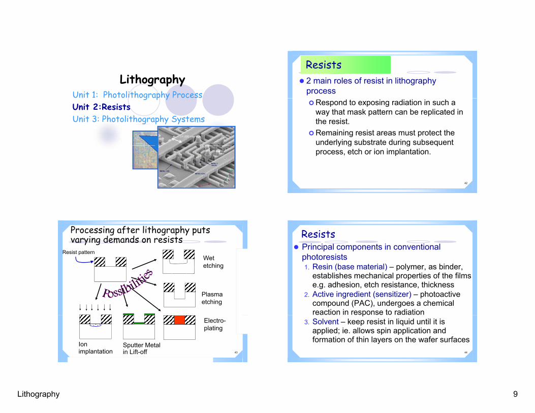
Resists 2 main roles of resist in lithography
processRespond to exposing radiation in such a
way that mask pattern can be replicated in the resist.
Remaining resist areas must protect the underlying substrate during subsequent
42
y g g qprocess, etch or ion implantation.
Processing after lithography puts varying demands on resists
Wet etching
Resist pattern
Plasma etching
etching
43
Ion implantation
Sputter Metal in Lift-off
Electro-plating
Resists Principal components in conventional
photoresists1 Resin (base material) – polymer as binder1. Resin (base material) polymer, as binder,
establishes mechanical properties of the films e.g. adhesion, etch resistance, thickness
2. Active ingredient (sensitizer) – photoactive compound (PAC), undergoes a chemical reaction in response to radiation
44
p3. Solvent – keep resist in liquid until it is
applied; ie. allows spin application and formation of thin layers on the wafer surfaces

Lithography 10
Positive Vs Negative ResistLight
Mask
Exposed PhotoresistSili Di id
Iluminated A
Positive resistdeveloped in the exposed region
Negative resistremain in the exposed
Silicon DioxideSilicon Substrate
Areas
Negative Resist :Rendered Insoluble
Positive Resist :Rendered Soluble
45
remain in the exposed region
Etched Film Patterns
Positive Resist
During exposure, photochemical
Positive Resist :Rendered Soluble
reaction weakens the polymer chains. Exposed resists becomes more soluble
in developing solutions. Development rate for the exposed resist
is faster than the unexposed resist.
46
is faster than the unexposed resist. Example of PAC: diazonaphthoquinone
(DNQ)
Negative Resist During exposures, polymer is
strengthen by random cross-linkage of main chains or
Negative Resist :Rendered Insoluble
linkage of main chains or pendant side chains.
Becoming less soluble, slower dissolving in organic and water-based developersE l f ti ti
47
Example of negative-acting, two-component resists: bis(aryl)azide rubber resists
Positive resist vs Negative resistCharacteristic Positive Negative
Adhesion to Si Fair ExcellentAvailable compositions
Many VastcompositionsContrast, Higher, e.g., 2.2 Lower, e.g., 1.5Cost More expensive Less expensiveDeveloper Aqueous based
(ecologically sound)Organic solvent
Influence of oxygen No YesLift off Yes Yes
48
Lift-off Yes Yes
Minimum feature 0.5 m and below 2 mPhotospeed Slower Faster

Lithography 11
Characteristic Positive NegativePinhole count Higher LowerPinholes in mask Prints mask pinholes Not so sensitive to
mask pinholesR id ft d l t M tl t 1 d Oft bl
… cont’d
Residue after development Mostly at < 1m and high aspect ratio
Often a problem
Sensitizer quantum yield, 0.2 to 0.3 0.5 to 1Step coverage Better LowerStrippers of resist over Oxide stepsMetal steps
AcidSimple solvent
AcidChlorinated solvent
d
49
compoundsSwelling in developer No YesThermal stability Good FairWet chemical resistance Fair Excellent
Most useful metrics1. Sensitivity Amount of dose or light energy
(mJ/cm2) to create the chemical change2. Resolution How fine a line the resist can reproduce
from an aerial image
50
Resolution is determined by contrast, thickness, swelling and contraction after development
Resist Sensitivity Input energy (mJ/cm2) required to cause
chemical response in resist, which results (after development) in the desired resist (a te de e op e t) t e des ed es stpattern
Higher sensitivity allows shorter exposure time but too high resist undergo thermal reaction at room temperature
Positive system = 0 2 to 0 3
51
Positive system = 0.2 to 0.3 Negative system = 0.5 to 1, making it
more sensitive than positive resists
= Quantum yield
Resist Profiles Photons strike resist at different angle Scattering at the reflective interface results in
overexposed of resist Negative resist: broadening of the remaining
resist features Positive resist: quenching of top resist leading to
better resolution
A. Negative
DEVELOPMENT STEP Exterior Scatter Zone
52
B. Positive resist image
A. Negative resist image
Exterior Scatter Zone

Lithography 12
Resist Profiles• Undercut difficult to form in positive resist, easy to
UsesProfile Dose Developer Influence R/ Ro γ
Ion Implant, lift-off. Not good for plasma etching. Often only obtained through image reversal
High (often with back scatter radiation)
Low >10 >6
A: Positive resists Undercut
95-110°
a)
form in negative resist• R = Develop’t rate of exposed region • Ro = Develop’t rate of unexposed
image reversal
Lift-off, Reactive ion etch wet etch Ion Beam etch Perfect fidelity
Typically for positive resists, wet etch,
Normal Dose
Low Dominant
Moderate <4
<3
5-10
<5
Vertical
Normal or overcut
75-95°
b)
°
c)
53
rate of unexposed region• = Resist contrast
metallization <20% resist loss
Permanent resists, larger devices, MEMS
Dominant Little Influence
<3<0.1
B: Negative resists Undercut
45-75°
Pattern Transfer (by additive metal lift off)
Liftoff process sequence
Identify the resist
Starting Si substrate
Apply Resist Identify the resist type used – positive
A discontinuity or gap in the metal deposit is necessary for solvent to get at
Apply Resist
Mask alignment and Exposure
After Chlorobenzene Soak and Development
54
gthe uncoated resist wall; Identify the resist profile type –undercut
Sputter Metal
Metallized patternLiftoff to remove resist
Resist Contrast, Critical in determining the smallest line width to
be patterned (ie. resolution) and profile A measure of the resist’s ability to distinguish A measure of the resist s ability to distinguish
light from dark areas in the aerial image the exposure system produces
Exposure Response Curve: Normalized resist thickness Vs Dose
is determined by the slope of the curve; it is
55
y pnot constant for a particular resist composition; it depends on bake times, temperatures before and after exposure, wavelength of light, etc.
Contrast curves
st re
mai
ningD0
rem
aini
ng
0.8
1.0 1.0
0.8
D100
Frac
tion
of re
si
(A)Fr
actio
n of
resi
st
0
0.2
0.4
0.6
10 100 1000Exposure dose (mJ/cm2)
D100
0.6
0.4
0.2
010 100 1000
Exposure dose (mJ/cm2) (B)
D0
Approx slope portion of curve by a straight line Line extends from lower energy dose for which all of the
resist is removed, i.e. at energy density called D100
Lowest energy to drive the photochemistry, is D0
(A)Exposure dose (mJ/cm ) Exposure dose (mJ/cm ) (B)

Lithography 13
Contrast, Higher gives sharper line edges
)/(log1
010010 DD
g g p g Typical is 2 to 4 How many times is D100 larger that D0, if is 2?
57
Critical Modulation Transfer Function CMTF is the min optical modulation
function necessary to obtain a pattern D fi iti CMTF Definition – CMTFresist
= If the MTF of an aerial image is less than
the CMTF, the image will not be resolved
110110
/1
/1
0100
0100
DDDD
the CMTF, the image will not be resolved 1.0 -
0.75 -
0.5 -
0.25 -
0
Comparison of Aerial Images
D100
Do
Position
Rel
ativ
e Ex
posu
re D
ose
Quality of aerial image and resist contrast combine to produce resist edge profile
Practice Problems1. Suggest another method of Pattern Transfer in
lieu of the additive lift off process.2. If you want to create metal features on wafers y
via lithography, only negative photoresist is used to pattern metal by additive lift-off. True or false.
3. A 0.6-m thick layer of a particular photoresisthas D0 = 40 mJ/cm2 and D100 = 85 mJ/cm2. (a) Calculate the resist contrast, . (b) Calculate
59
Calculate the resist contrast, . (b) Calculate the CMTF. Ans: 3.05 & 0.36
4. Show that: 110110
/1
/1
0100
0100
DDDDCMTFresist
Blank page
65

Lithography 14
Lithography
Unit 1: Photolithography ProcessUnit 2: ResistsUnit 3: Photolithography SystemsUnit 3 Photolithography Systems
(5)
ResistSiO2
Maskhv
n - Si
Photolithography Systems Corner stone of
wafer processingE t Exposure systems –3 types
Performance parameters –projection systemprojection system
Technology Scaling 0.18-micron & 0.13-micron technology are used
to make IC; latest is the 90 nanometer technology – what does it mean? gy
Technology node to describe the minimum feature size
Critical Dimension (CD) – Minimum feature size in IC or miniature device and it is a measure of the resolution of a lithographic process (e.g. line width spacing contact dimension)line width, spacing, contact dimension)
Overall Resolution of a process – Ability to print a minimum size image, a critical dimension, under conditions of reasonable manufacturing variation
Energy Sources – waves or particles Energy sources are required to modify the resist The energy source is aerial imaged on the resist Bright sources are usually required for high Bright sources are usually required for high
throughputWavelength Energy
Light UV 400 nm 3.1 eV
Deep UV 250 nm 4 96 eVDeep UV 250 nm 4.96 eVX-Ray 0.5 nm 2480 eV
Particles Electrons 0.62 Å 20 keVIons 0.12 Å 100 keV

Lithography 15
Photolithography – printing methods Optical-based - three exposure systems
1. Contact Printing2 Proximity Printing2. Proximity Printing3. Projection Printing
Comparison of three exposure systemsLight intensity profile forthree exposure systems
OpticalSystem
LightSource
(1) Contact (2) Proximity (3) Projection
1.2 II
Mask
SiliconWafer
Photoresist
Mask
System
Gap0
0.2 I
0.4 I
0.6 I
0.8 I
I (1) Contact(2) Proximity
(3) Projection
1. Contact Printing Photo-resist covered
wafer, put in intimate contact with photomask, exposed with
Ilumination lightexposed with broadband-visible and near UV light
Defects on mask, due to repeated mask-to-wafer contacting steps
Mask image: Resist
Condensor lensCondensor lens
Mask patternPhotoresistWafer
Contact
Mask image: Resist image is 1:1, not limited by diffraction
Not applicable to VLSI and ULSI
2. Proximity Printing
Mask is placed in closed proximity, gap Ilumination light
Gap
about 2-20 µm to wafer Avoid mask damage Limited by near field
(Fresnel) diffraction of transmitted light;
Condensor lens
Mask pattern
PhotoresistWafer transmitted light;
reduces resolutionMinimum feature size
about 3 µm
Wafer
Resolution: min resolvable feature size
Generally, resolution in shadow printing
3 zsbR (1)
Incident UV light on mask
Mask plate
bmin = half the grating periods = gap between mask & resist = incident wavelengthz = resist thickness
Contact Printing
22min sbR
3
(1)
b b bs
p
Mask pattern
Resist
Wafer
Ideal transferA t l
Proximity Printing, s >> z22
3min
zbR
sbR 23
min (3)
(2)
0 1 2 3
Actual transfer
Sb 32 min
POSITION ON WAFER
4
b b bMinimum period transferable

Lithography 16
Example on Proximity PrintingGap,s = 10 m; = 400 nm From Eq.(3) R = bmin = 3 m sbR
23
min
Limitation: Practical UV proximity printing is about 2 to 3 m
In contact printing: If thickness resist, z = 1 m, from Eq.(2) R = bmin = 0.67 m(for extremely flat wafers) 3 z(for extremely flat wafers)
223
minzbR
3. Projection PrintingUse of imaging (projection)
optics in between the mask and the wafer
Ilumination light
Condensor lens
k1 = empirical constant NA
k 1min
bR
Limited by far field (Fraunhofer) diffraction Modified Rayleigh criterion
Condensor lens
Mask pattern
Diffracted lightProjection lens
(resists, process and mask aligner optics)
NA = numerical aperture of projection lens system
PhotoresistWafer
Projection printers: Performance Parameters
1. Resolution Determined by optical system, resist, etch
process2. Alignment accuracy Alignment of pattern to previous layer is to
ensure overlay is within the specification Determined by the optical system and Determined by the optical system and
aligner3. Throughput How many wafers/hour Determined by optical system, resist
Rayleigh Resolution (Fraunhofer diffraction pattern) - 1 Rayleigh criterion defines that two images are
just resolved when the maximum intensity of the first Airy disk falls on the first zero intensity offirst Airy disk falls on the first zero intensity of the second disk
Where n = refraction index
sin 0.61
) sin 2( f 1.22
Df 22.1
nfnR
Where n refraction index of material (usually air with n = 1 for the system); = max half-angle of diffracted light = wavelength

Lithography 17
Numerical Aperture NA characterizes the ability
of lens to transmit light, θsin nNA
Mask
2D
2D θ and
air)(for 1 Since
2D
fNA
ff
n
f
D
Projector
Wafer 2 fEffective F-number = Focal Length (f)
Clear Aperture (D)= 1/ (2 NA)
Wafer
NA DNA = 0, Lens collects no lightNA = 1, Lens collects all light
Rayleigh Resolution (Fraunhofer diffraction pattern) - 2
610
:gives
0.61 into sin n ngSubstituti
sinnRNA
0.61 factor is based on Fraunhofer diffraction pattern for an Airy disk using point
NANAR k 61.0
1
sources k1 is used in actual system; 0.6 to 0.8
Resolution – three ways to improve
NAR k ,Resolution 1
Lower k1
Smaller Light source
Ability of resist to distinguish between small changes in intensity; Improved optical
Higher NA
intensity; Improved optical schemesLens design improvements;Limited by lens aberrations
Problems Calculate the resolution by a 0.65 NA lens when
i-line wavelength is used. Assume k1 = 0.6.R = k / NAR = k1 / NAAns: R = 0.34 µm
Repeat the calculations for 0.75 NA lens when (c) DUV 248 nm (d) DUV 193 nm wavelength is used. Assume k1 = 0.4.
ANS: (c) 0.13 µm (d) 0.10 µm

Lithography 18
Depth of Focus To obtain good line width control, the image must
remain in focus through the depth of the resist layer If DOF, is the on-axis path length difference at the limit
of focus, then the path length difference for a ray from , p g ythe edge of the entrance aperture (mask window) is simply cos.
Rayleigh criteria for DOF: difference of these two lengths is not more than /4
(MASK) Object plane Lens
lm
Best focusing plane
(Wafer) Image plane
Lens axisDOF,
Simple image system
D
f
Depth of Focus (DOF)22
0
2
2 - 1 - 1 cos -
4
DOF becomes an issue
2
5.0 ,DOF f 2
D sin ,SinceNA
NA
22 DOFNA
k
Decreases as Decreases as k2 Decreases as NA
Example: Estimate the resolution and depth of focus of an excimer stepper using KrF light source (=248 nm) with a NA=0.6. Assume k1=0.75 and k2=0.5.
μm 0.34
0.60.248 0.5 k
μm 0.31 0.6
0.248 0.75 k
222
1
NADOF
NAR
What is maximum possible resist layer thickness?What is maximum possible resist layer thickness? Note that very flat topography is requiredMax resist layer thickness isSuggest other methods to improve R other than
improving the light source. Ans: optical methods
0.34 m
Modulation Transfer Function (MTF) Diffraction effects, interference, dark regions in
the image never reach complete darkness, i.e. intensity = 0intensity = 0
Quality of image, modulation index, M is defined as
Use to characterize the capability of projection system to reproduce mask feature on wafer
minmax
minmax
IIIIMTFim
surface Ideal case, MTFim=1 Practical case, MTFim<1

Lithography 19
Modulation Transfer Function (MTF)Incident UV light on mask
b b b
Mask plate
Mask patternb b b
Resist
Wafer
Ideal transfer, Mmask= 1
LensIncident UV light on Resist
Res
ist
0 1 2 3
Actual transfer, Mim
POSITION ON WAFER (Arbitrary Units)
4
b b bminmax
minmaxim
IIIIMTF
Inci
dent
Inte
nsity
on
R
Imax
Imin
MTF What is MTF? A measure of the contrast in
the aerial image produced by the exposure systemsystem
Generally MTF 0.5 for resist to resolve features
Value is dependent on (a) feature size in the image (b) spatial coherence of the light source
5
Spatial coherence – a measure of degree to which light emitted from the light source stays in phase at all points along the emitted wave fronts.
MTF MTF
L S ll0
1
1
Light Source (point source)
CondensorLens
Light Source (area)
CondensorLens
sMTF versus feature size in the image.
LargerFeatures
SmallerFeatures SizeFeature
Waves are in phase
Examples of spatially coherent (left) and partially coherent (right) light sources.
Lens
Mask
Lens
Mask
D
Manufacturing Methods and Equipment: Projection Methods
1. Scannero 1:1 scanning projection aligners first use in
1970s; capability of 1-m features and1970s; capability of 1 m features and throughput of 110 wafers/hr (WPH)
2. Step-and-repeat (stepper) Projection ratio of 4:1 reduction lens; capable
of 0.13 m production and 30 WPH throughput; alignment of each chip individually;
St d ( i t h b id)3. Step-and-scan (scanning stepper or hybrid) Reduction lenses makes mask-making much
easier and gives tighter line-width tolerance on wafer
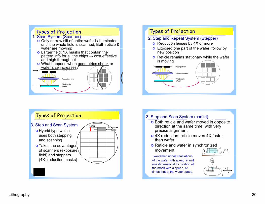
Lithography 20
Types of Projection1. Scan System (Scanner) Only narrow slit of entire wafer is illuminated
until the whole field is scanned; Both reticle & wafer are moving;wafer are moving;
Larger field; 1X masks that contain the pattern info for all the chips cost effective and high throughput
What happens when geometries shrink or wafer size increases?
Mask pattern
Projection lens
PhotoresistWafer
Types of Projection2. Step and Repeat System (Stepper) Reduction lenses by 4X or more Exposed one part of the wafer follow by Exposed one part of the wafer, follow by
new position Reticle remains stationary while the wafer
is movingMask pattern
Projection lens
PhotoresistWafer
3. Step and Scan SystemHybrid type which
Types of Projection
Exposure Field
Scan
y ypuses both stepping and scanning
Takes the advantages of scanners (exposure field) and steppersfield) and steppers (4X- reduction masks)
3. Step and Scan System (con’td) Both reticle and wafer moved in opposite
direction at the same time, with very precise alignment p g
4X reduction: reticle moves 4X faster than wafer
Reticle and wafer in synchronized movement
Two dimensional translations
M υR
Two-dimensional translations of the wafer with speed, v and one dimensional translation of the mask with a speed, Mtimes that of the wafer speed.
υ
R

Lithography 21
Step and Scan System: ASML PAS 5500/950B
Reticle (Mask)
193 nm Excimer Laser Source Computer
Console
Exposure Column(Lens)
Wafer
Alignment in Photolithography
RECAP
Alignment and Overlay Overlay – general pattern placement; each level
must be aligned to the previous levels; Alignment – specific spots on the wafer; it is g p p ;
limited to specific structures (chip edge) and it not a full guarantee of overlay elsewhere
Overlay is the outcome of alignment Overlay tolerance requirement is 1/3 of the min
feature size E g overlay tolerance to print x m min linewidth E.g. overlay tolerance to print x m min linewidth
structure is capable of x/3 m registration between levels
Global Alignment & Local Alignment
o
a
A 5X projection stepper with 0.5 m min lines is capable of 0.16 m registration between levels

Lithography 22
Summary: Resolution Limit
Maskbbs
2z
23
min bR1) Contact
2) Proximity sbR 23
min
ResistFilm
bbsz
2) Proximity
3) Projection2min
NAbR 1k
min 22
)(kNA
DOF
Photolithograph Resolution Enhancement Technology (RET)
Present: Current lithography techniques g p y quse deep ultraviolet range 248 nm wavelengths to print 150 to 120 nm size features
Future: New techniques to create smaller featuresfeatures
Cost of lithography in IC production: 35% of total chip cost
Moore’s Law in IC Fabrication Gordon Moore, former chairman of Intel
states that the number of transistors per square cm doubles every two years without q y yincrease in cost.
http://news.bbc.co.uk/2/hi/technology/7080646.stm
Resolution Enhancement Technique (RET) Improve the resolution by Mask
engineering1 Optical Proximity Correction (OPC)1. Optical Proximity Correction (OPC)2. Phase-Shifting Mask (PSM)3. Off-Axis Illumination (OAI) 4. Immersion

Lithography 23
Improvement of R (Extension of Photolithography)
Wavelength 365nm 248nm 193nm 157nm Deep UV Excimer Laser Sources
gi-line KrF ArF F2
NA Method
k1 0.65 0.70 0.80 0.70 0.85 0.70 0.85
Conventional 0.6 335nm 213 185nm
Off axis ill i i
0.5 280nm 177 155nm 138 115nm 110 90nm illumination
Strong OAI + OPC and/or PSM
0.4 142 125nm 110 90nm 90 75nm
1. Optical Proximity Correction (OPC)
Feature distortion (edges of printed or etched features do not conform to those of the designed patterns) incurred in thethe designed patterns) incurred in the pattern transfer process
- Example: corner rounding, line shortening
OPC is used to pre-compensate the reticle/mask pattern to account for expectedreticle/mask pattern to account for expected pattern distortion due to diffraction effect
Adding serifs enhance the amount of light transmitted through the corner
Cont’d OPC
Mask with OPC
PatternPattern (without OPC) Pattern
2. Phase Shifting Mask (PSM) Improved mask technology: most dramatic
improvement in resolution that can be contributed by reticlecontributed by reticle
Without PSM: NA=0.6, =0.248 nm, CD=0.3 µmWith PSM: CD can be improved to 0.18 µm
Concept of improving resolution by modifying the optical phase of the mask transmission was first suggested in 1982 by Levensonfirst suggested in 1982 by Levenson

Lithography 24
Alternating Phase Shifting Mask (AltPSM)
Adding an extra layer of transmissive material to the optical path
Basically involves the Amplitude at Mask
180° Phase Shift
PSMChrome
ydestructive interference of light occurring along the transition edge between the 0 and 180 phase-shifted areas.
Better resolution and
at Mask
Amplitude at Wafer
contrast can be achieved due to destructive interference between the two adjacent diffracted wavefronts. (After Levenson)
Intensity at Wafer
Conventional Phase-shift mask
3. Off-Axis Illumination (OAI)
Incorporated into steppers in 1992 OAI = Illumination light strike the projectionOAI Illumination light strike the projection
lens at the edge of entrance pupil Conventional illumination, light strike the
center of lens Imaging ≤ 0th order + one additional
diffracted order
Cont’d - OAI R is improved by letting light impinging at an
angle to the mask to capture higher-order diffracted light
ApertureProjection
Lens ApertureProjection
Lens
“Capture” Diffracted
Light
“Lost” Diffracted
Light Wafer“Capture” Diffracted
Light
“Lost” Diffracted
Light Wafer
On-axis illumination (left) and off-axis illumination (right) (Plummer p.237)
Limits of Optical Lithography CD of optical lithography With RETs, CD 30% smaller than exposure wavelength, i.e.
0.18 µm for 248 nm wavelength Rate of shrinkage of CD faster than reduction of exposure
NAb 1
mink
g p Current DUV generation: 193 nm with combinations of PSM
and OAI can be extended to beyond 100 nm
0.8
0.9
0.7
G-linel-line
248nm193nm
1.0
0.8
0 6Ape
rture
Physical limit for air
l-line248nm
0.6
0.5
0.4
0.3
k1
1982 1985 1990 1995 2000
193nm
Year of system introduction
0.6
0.4
0.2
0.0
Num
eric
al A
1980 1985 1990 1995 2000
G-linel line

Lithography 25
4. Immersion Lithography (IL)
Recap:DθsinnNA
Liquid recovery
Projection optics Liquid
supply 2
θsin f
nNA
Where n is the refractive index of the medium surrounding the lens and is the acceptance
l f th l
Wafer stage
(Scanning motion)Immersion liquid
Wafer
angle of the lens. Sine of any angle is always ≤ 1 and n =1 for air What if a medium with a higher index of
refraction is substituted with air?
IL – refractive index Refractive index, n > 1 Ultrapure water, n 1.47 (it has low optical
b ti tibl ith i t dabsorption, compatible with resist and non-contaminating
sin k k
11
min nNAb
Increase n improves resolutionIncrease n improves resolution
Issues – presence of bubbles; cause light scattering
Next Generation Lithography (NGL)
Energy Source1. Extreme
UltravioletUltraviolet (EUV); 20 nm
2. X-Ray Lithography; 1 nm
3. Charged-P ti lParticle Beam (E-beam and Ion beam); 0.1 nmOthers: Nanoimprint for lithography and Soft lithography
Summary of Lithography Components of
Lithography Energy – modify resist gy y
dissolution rate; UV, DUV, X-ray, E-beam
Mask – pattern energy to resist; transparent + opaque
Exposure systems/ aligner – contact, proximity, projection, optics; resolution
Resist

Lithography 26
Practice Problems1. It has been determined that there are no clear
choices for lithography systems beyond optical projection tools based on 193-nm ArF excimerlasers One possibility is an optical projectionlasers. One possibility is an optical projection system using 157-nm F2 excimer laser.
a. Assuming a numerical aperture of 0.8 and k1=0.75, what is the expected resolution of such a system using a first order estimate of resolution? Ans: 147 nm
b. Actual projections for such systems suggest that they might be capable of resolving features suitable for the 2009 70 nm generation Suggest three approaches to2009 70 nm generation. Suggest three approaches to actually achieving this resolution with these systems? Hint: refer to the resolution equation and section on RET
2. In a 4X reduction scanner lithography system, the wafer must move 4 times faster than the
ti l T f l ?reticle. True or false?3. Once the _______ image has been formed in
the polymer film after exposure, it must be developed to produced the final 3-D ______ image.