resonant modes of single silicon nanocavities excited by ... · resonant modes of single silicon...
TRANSCRIPT
COENEN ET AL. VOL. XXX ’ NO. XX ’ 000–000 ’ XXXX
www.acsnano.org
A
CXXXX American Chemical Society
Resonant Modes of SingleSilicon Nanocavities Excitedby Electron IrradiationToon Coenen,† Jorik van de Groep,†,* and Albert Polman
Center for Nanophotonics, FOM Institute AMOLF, Science Park 104, 1098 XG Amsterdam, The Netherlands, †These authors contributed equally to this work.
Nanoparticles and nanowires madefrom high-index semiconductor ordielectric materials have the ability
to strongly confine and scatter light.1�4 Theseproperties make them interesting for a largerange of applications including solar cells,5�14
lasers,15 and nanoscale photodetectors orsensors.16�20 Unlike their metallic counter-parts, where light is confined to the surfacein the form of surface plasmons, in semi-conductor/dielectric nanostructures, light ismostly confined within the nanostructure.The resonant eigenmodes of these cavitiesare often referred to as Mie resonances,after the Lorentz�Mie�Debye solution toMaxwell's equations, which can be used todescribe scattering by wavelength-scalespherical nanoparticles in a uniform dielec-tric environment.1 They can also be referredto as geometrical resonances because oftheir similarity towhisperinggallerymodes.7,21
Silicon is an ideal base material for reso-nant Mie cavities. Due to its high refrac-tive index, it can strongly confine light,while its indirect electronic band gap leadsto relatively low absorption losses. Due to the
compatibilitywithCMOS fabricationprocesses,resonant Si Mie scatterers can be readilyintegrated into optoelectronic devicesbased on silicon. The first applications ofsilicon Mie scatterers in metamaterials,22�24
optical antennas,2,22,25�27 and anti-reflectioncoatings2 are appearing just recently andshow the great potential of Mie scatterersas optical building blocks in nanophotonicnanostructures and devices. To fully unleashthe potential of these nanoscale Si light scat-terers, detailed understanding of their funda-mental scattering properties is essential.However, standard optical techniques havebeen unable to fully resolve the Mie resonantmodes due to lack of spatial resolution.In this article, we study the resonant
optical properties of individual silicon cylin-ders using angle-resolved cathodolumi-nescence (CL) imaging spectroscopy.28�30
With this technique, a 30 keV electronbeam acts as a broad-band point sourceof light that can be employed to probethe optical properties of nanostructureswith deep-subwavelength spatial resolu-tion.31,32 We determine the spectral and
* Address correspondence [email protected].
Received for review December 10, 2012and accepted January 11, 2013.
Published online10.1021/nn3056862
ABSTRACT High-index dielectric or semiconductor nanoparticles support strong Mie-like geome-
trical resonances in the visible spectral range. We use 30 keV angle-resolved cathodoluminescence
imaging spectroscopy to excite and detect these resonant modes in single silicon nanocylinders with
diameters ranging from 60 to 350 nm. Resonances are observed with wavelengths in the range of
400�700 nm, with quality factors in the range Q = 9�77, and show a strong red shift with increasing
cylinder diameter. The photonic wave function of all modes is determined at deep-subwavelength
resolution and shows good correspondence with numerical simulations. An analytical model is
developed that describes the resonant Mie-like optical eigenmodes in the silicon cylinders using an
effective index of a slab waveguide mode. It shows good overall agreement with the experimental
results and enables qualification of all resonances with azimuthal (m = 0�4) and radial (q = 1�4)
quantum numbers. The single resonant Si nanocylinders show characteristic angular radiation
distributions in agreement with the modal symmetry.
KEYWORDS: cavity . nanoantennas . dielectric . cathodoluminescence spectroscopy . Mie resonance . point dipole emitter .electron beam . silicon photonics . Fourier microscopy
ARTIC
LE
COENEN ET AL. VOL. XXX ’ NO. XX ’ 000–000 ’ XXXX
www.acsnano.org
B
spatial characteristics of the resonant optical eigen-modes for single silicon nanocylinders with differentdiameters. We compare our results with finite-differencetime-domain (FDTD) simulations andananalyticalmodel,and we identify the fundamental and higher-orderradial and azimuthal modes of the cavities. In addition,we present experimental data on the angular distribu-tion and polarization of light emission from singleresonant Mie cavities.
RESULTS AND DISCUSSION
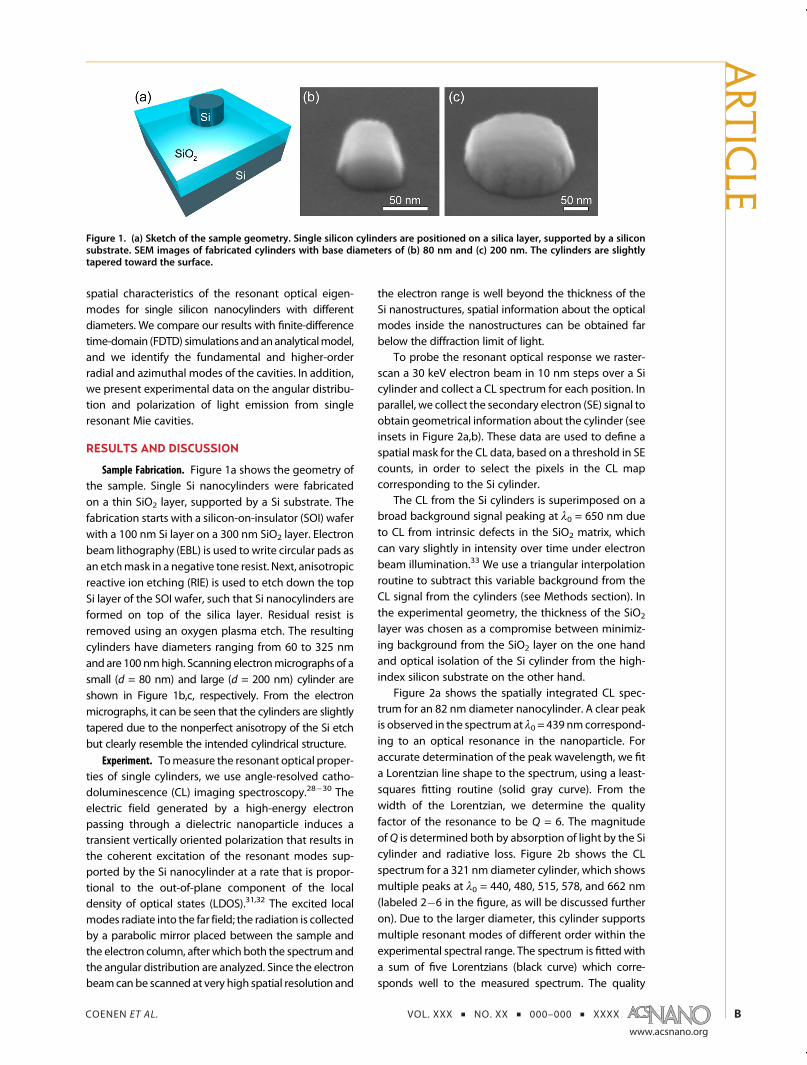
Sample Fabrication. Figure 1a shows the geometry ofthe sample. Single Si nanocylinders were fabricatedon a thin SiO2 layer, supported by a Si substrate. Thefabrication starts with a silicon-on-insulator (SOI) waferwith a 100 nm Si layer on a 300 nm SiO2 layer. Electronbeam lithography (EBL) is used to write circular pads asan etchmask in a negative tone resist. Next, anisotropicreactive ion etching (RIE) is used to etch down the topSi layer of the SOI wafer, such that Si nanocylinders areformed on top of the silica layer. Residual resist isremoved using an oxygen plasma etch. The resultingcylinders have diameters ranging from 60 to 325 nmand are 100 nmhigh. Scanning electronmicrographs of asmall (d = 80 nm) and large (d = 200 nm) cylinder areshown in Figure 1b,c, respectively. From the electronmicrographs, it can be seen that the cylinders are slightlytapered due to the nonperfect anisotropy of the Si etchbut clearly resemble the intended cylindrical structure.
Experiment. Tomeasure the resonant optical proper-ties of single cylinders, we use angle-resolved catho-doluminescence (CL) imaging spectroscopy.28�30 Theelectric field generated by a high-energy electronpassing through a dielectric nanoparticle induces atransient vertically oriented polarization that results inthe coherent excitation of the resonant modes sup-ported by the Si nanocylinder at a rate that is propor-tional to the out-of-plane component of the localdensity of optical states (LDOS).31,32 The excited localmodes radiate into the far field; the radiation is collectedby a parabolic mirror placed between the sample andthe electron column, after which both the spectrum andthe angular distribution are analyzed. Since the electronbeamcanbe scanned at very high spatial resolution and
the electron range is well beyond the thickness of theSi nanostructures, spatial information about the opticalmodes inside the nanostructures can be obtained farbelow the diffraction limit of light.
To probe the resonant optical response we raster-scan a 30 keV electron beam in 10 nm steps over a Sicylinder and collect a CL spectrum for each position. Inparallel, we collect the secondary electron (SE) signal toobtain geometrical information about the cylinder (seeinsets in Figure 2a,b). These data are used to define aspatial mask for the CL data, based on a threshold in SEcounts, in order to select the pixels in the CL mapcorresponding to the Si cylinder.
The CL from the Si cylinders is superimposed on abroad background signal peaking at λ0 = 650 nm dueto CL from intrinsic defects in the SiO2 matrix, whichcan vary slightly in intensity over time under electronbeam illumination.33 We use a triangular interpolationroutine to subtract this variable background from theCL signal from the cylinders (see Methods section). Inthe experimental geometry, the thickness of the SiO2
layer was chosen as a compromise between minimiz-ing background from the SiO2 layer on the one handand optical isolation of the Si cylinder from the high-index silicon substrate on the other hand.
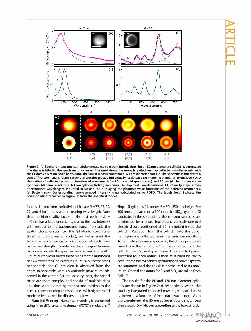
Figure 2a shows the spatially integrated CL spec-trum for an 82 nm diameter nanocylinder. A clear peakis observed in the spectrum at λ0 = 439 nmcorrespond-ing to an optical resonance in the nanoparticle. Foraccurate determination of the peak wavelength, we fita Lorentzian line shape to the spectrum, using a least-squares fitting routine (solid gray curve). From thewidth of the Lorentzian, we determine the qualityfactor of the resonance to be Q = 6. The magnitudeofQ is determined both by absorption of light by the Sicylinder and radiative loss. Figure 2b shows the CLspectrum for a 321 nm diameter cylinder, which showsmultiple peaks at λ0 = 440, 480, 515, 578, and 662 nm(labeled 2�6 in the figure, as will be discussed furtheron). Due to the larger diameter, this cylinder supportsmultiple resonant modes of different order within theexperimental spectral range. The spectrum is fitted witha sum of five Lorentzians (black curve) which corre-sponds well to the measured spectrum. The quality
Figure 1. (a) Sketch of the sample geometry. Single silicon cylinders are positioned on a silica layer, supported by a siliconsubstrate. SEM images of fabricated cylinders with base diameters of (b) 80 nm and (c) 200 nm. The cylinders are slightlytapered toward the surface.
ARTIC
LE
COENEN ET AL. VOL. XXX ’ NO. XX ’ 000–000 ’ XXXX
www.acsnano.org
C
factors derived from the individual fits areQ= 77, 27, 29,22, and 9 for modes with increasing wavelength. Notethat the high quality factor of the first peak at λ0 =440 nm has a large uncertainty due to the low intensitywith respect to the background signal. To study thespatial characteristics (i.e., the “photonic wave func-tions” of the resonant modes), we determined thetwo-dimensional excitation distribution at each reso-nance wavelength. To obtain sufficient signal-to-noiseratio, we integrate the spectra over a 20 nm bandwidth.Figure 2e (top row) shows thesemaps for the numberedpeakwavelengths indicated in Figure 2a,b. For the smallnanoparticle, the CL emission is observed from theentire nanoparticle, with an antinode (maximum) ob-served in the center. For the large cylinder, the spatialmaps are more complex and consist of multiple ringsand dots with alternating minima and maxima in thecenter, corresponding to resonances with higher radialmode orders, as will be discussed below.
Numerical Modeling. Numerical modeling is performedusing finite-difference time-domain (FDTD) simulations.34
Single Si cylinders (diameter d = 50�350 nm, height h =100 nm) are placed on a 300 nm thick SiO2 layer on a Sisubstrate. In the simulations, the electron source is ap-proximated by a single broad-band vertically orientedelectric dipole positioned at 50 nm height inside thecylinder. Radiation from the cylinder into the upperhemisphere is collected using transmission monitors.To simulate a resonant spectrum, the dipole position isvaried from the center (r = 0) to the outer radius of thecylinder (r = d/2), in steps of 5 nm. The collected powerspectrum for each radius is then multiplied by 2πr toaccount for the cylindrical geometry; all power spectraare summed, and the result is normalized to its max-imum. Optical constants for Si and SiO2 are taken fromPalik.35
The results for the 80 and 320 nm diameter cylin-ders are shown in Figure 2c,d, respectively, where thespatially integrated collected power (green solid lines)is shown as a function of free space wavelength. As inthe experiment, the 80 nm cylinder clearly shows onesingle peak (Q= 16), corresponding to the lowest-order
Figure 2. (a) Spatially integrated cathodoluminescence spectrum (purple dots) for an 82 nm diameter cylinder. A Lorentzianline shape is fitted to the spectrum (gray curve). The inset shows the secondary electron map collected simultaneously withthe CL data collection (scale bar: 50 nm). (b) Similarmeasurement for a 321 nmdiameter particle. The spectrum is fittedwith asum of five Lorentzians (black curve) that are also plotted individually (scale bar SEM image: 150 nm). (c) Normalized FDTDsimulation of collected power as function of wavelength for 80 nm (solid green curve) and 70 nm (dashed green curve)cylinders. (d) Same as (c) for a 321 nm cylinder (solid green curve). (e, Top row) Two-dimensional CL intensity maps shownat resonance wavelengths indicated in (a) and (b), displaying the photonic wave functions of the different resonances.(e, Bottom row) Corresponding time-averaged intensity maps calculated using FDTD. The labels [m,q] indicate thecorresponding branches in Figure 3b from the analytical model.
ARTIC
LE
COENEN ET AL. VOL. XXX ’ NO. XX ’ 000–000 ’ XXXX
www.acsnano.org
D
resonance, whereas the 320 nm cylinder shows manypeaks due to higher-order resonances. Compared withthe experiment for the 80 nm cylinder, the simulatedpeak wavelength is off by 18 nm. We attribute thisto the small tapering of the cylinders, resulting in aslightly reduced diameter at the surface, as can beobserved in Figure 1b,c. Indeed, the simulated spec-trum for a 70 nm diameter (dashed line) matches themeasured spectrum quite well. This indicates that theeffective diameter of a particle with an 80 nm diameterbase is 70 nm, in good correspondence with the SEMimage in Figure 2a. The simulated spectrum for the320 nm diameter particle in Figure 2d shows goodagreement with the different resonances with theexperiment. In agreement with the experiment, thesimulated peak at λ0 = 575 nm has the highestintensity. The simulated quality factor for the fivemodes is Q = 21, 19, 24, 30, and 15, which is in thesame range as the experimental values, except for thesmall lowest-wavelength peak. The observed Q isdetermined by both absorption in the particle andthe radiative coupling to the far field. Absorption lossesare larger in the blue spectral range due the higherabsorption of silicon in that wavelength range.
Figure 2e, bottom row, shows the simulated time-averaged photonic wave functions. Analogous to theexperiment, the peak intensity is integrated over a20 nm bandwidth around the peak wavelength for
each dipole position, giving the peak intensity as afunction of radial position. The data set is then rotatedto obtain the two-dimensional photonic wave functionmaps. Simulations are shown for the 80 and 320 nmdiameter cylinders for each resonance. The simulatedphotonic wave function of the lowest-order mode forthe 82 nm cylinder (peak 1) shows a bright ring, whilethe measurement shows a more uniform distributionpeaking in the center. For the 320 nm cylinder, thesimulations show good agreement with the measuredtrends. For lower resonance wavelengths (going frompeak 2 to peak 6), more nodes and antinodes areobserved in the radial direction, corresponding tohigher-order radial modes. For the highest-ordermode(peak 6), a bright dot is observed in the center,surrounded by two bright rings. The alternating darkand bright center of the cylinder observed for subse-quent resonances is also reproduced in the simulations.
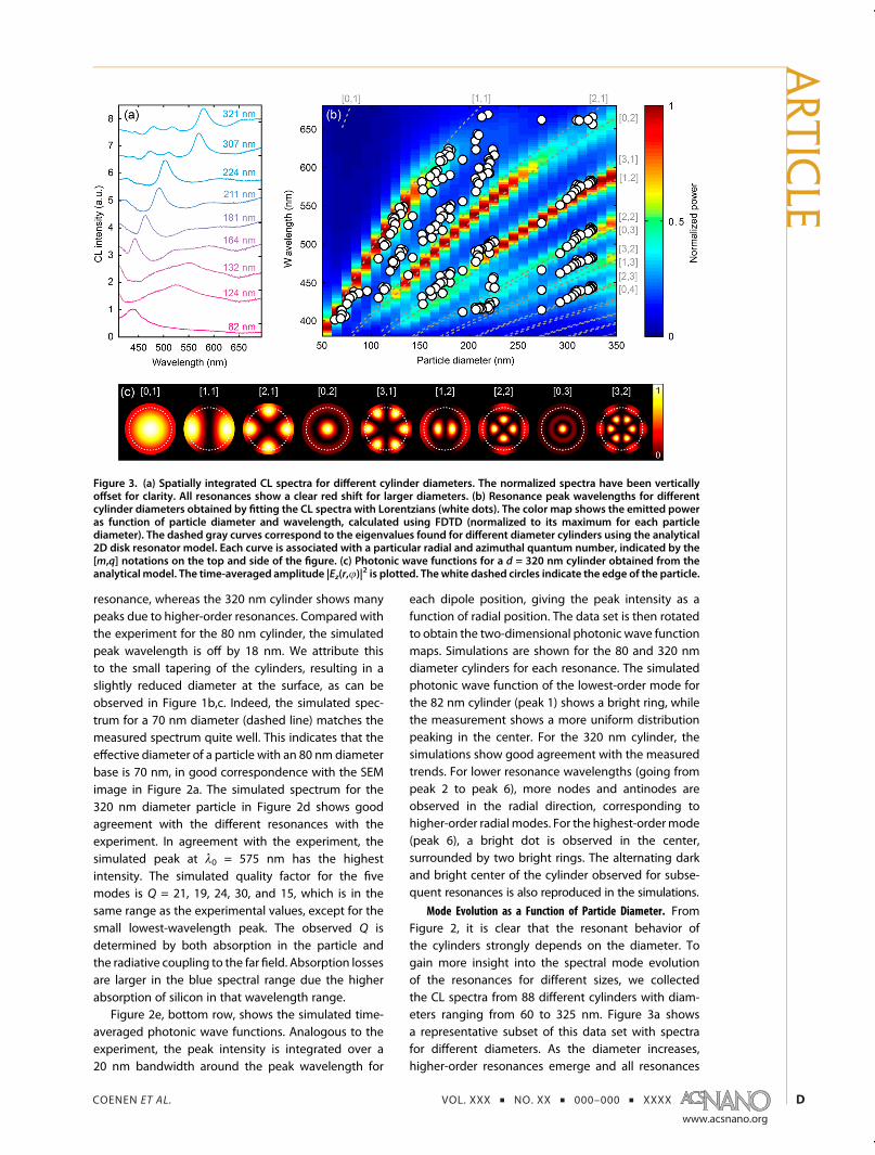
Mode Evolution as a Function of Particle Diameter. FromFigure 2, it is clear that the resonant behavior ofthe cylinders strongly depends on the diameter. Togain more insight into the spectral mode evolutionof the resonances for different sizes, we collectedthe CL spectra from 88 different cylinders with diam-eters ranging from 60 to 325 nm. Figure 3a showsa representative subset of this data set with spectrafor different diameters. As the diameter increases,higher-order resonances emerge and all resonances
Figure 3. (a) Spatially integrated CL spectra for different cylinder diameters. The normalized spectra have been verticallyoffset for clarity. All resonances show a clear red shift for larger diameters. (b) Resonance peak wavelengths for differentcylinder diameters obtained by fitting the CL spectra with Lorentzians (white dots). The color map shows the emitted poweras function of particle diameter and wavelength, calculated using FDTD (normalized to its maximum for each particlediameter). The dashed gray curves correspond to the eigenvalues found for different diameter cylinders using the analytical2D disk resonator model. Each curve is associated with a particular radial and azimuthal quantum number, indicated by the[m,q] notations on the top and side of the figure. (c) Photonic wave functions for a d = 320 nm cylinder obtained from theanalytical model. The time-averaged amplitude |Ez(r,j)|
2 is plotted. The white dashed circles indicate the edge of the particle.
ARTIC
LE
COENEN ET AL. VOL. XXX ’ NO. XX ’ 000–000 ’ XXXX
www.acsnano.org
E
progressively red shift as is expected for geometricalresonances.1
By using the Lorentzian fitting shown in Figure 2a,b,we determined the resonance peak wavelength for allmeasured cylinders. In Figure 3b, these peak wave-lengths are shown as a function of diameter. This figureclearly shows how each resonance mode gradually redshifts for increasing diameter. To compare the experi-mental resonances with the results from numericalmodeling, we also plot the collected power as afunction of diameter and wavelength in a 2D colorplot (Figure 3b). Here, every vertical slice in the colorplot corresponds to a normalized spectrum, as shownin Figure 2c,d. The FDTD simulations show multiplebranches, each of which corresponds to a particularresonant mode in the cylinders. Both the number ofpeaks as well as their peak wavelength show goodagreement with themeasurements, except the secondbranch from the top, for which the simulation is blue-shifted with respect to the measurements.
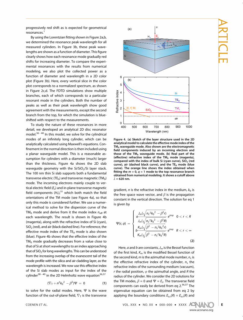
To study the nature of these resonances in moredetail, we developed an analytical 2D disc resonatormodel.36�40 In this model, we solve for the cylindricalmodes of an infinitely long cylinder, which can beanalytically calculated using Maxwell's equations. Con-finement in the normal direction is then included usinga planar waveguide model. This is a reasonable as-sumption for cylinders with a diameter (much) largerthan the thickness. Figure 4a shows the 2D slabwaveguide geometry with the Si/SiO2/Si layer stack.The 100 nm thin Si slab supports both a fundamentaltransverse electric (TE0) and transverse magnetic (TM0)mode. The incoming electrons mainly couple to ver-tical electric field (Ez) and in-plane transverse magneticfield components (HT),
31 which both match the fieldorientations of the TM mode (see Figure 4a), so thatonly this mode is considered further. We use a numer-ical method to solve for the dispersion curve of theTM0 mode and derive from it the mode index neff ateach wavelength. The result is shown in Figure 4b(magenta), along with the refractive index of Si (cyan),SiO2 (red), and air (black dashed line). For reference, theeffective mode index of the TE0 mode is also shown(blue). Figure 4b shows that the effective index of theTM0 mode gradually decreases from a value close tothat of Si at short wavelengths to an index approachingthat of SiO2 for longwavelengths. This canbeunderstoodfrom the increasing overlap of the evanescent tail of themode profile with the silica and air cladding layer, as thewavelength is increased. We now use this effective indexof the Si slab modes as input for the index of thecylinder38�40 in the 2D Helmholtz wave equation36,37
(rT þ n2k02 � β2)Ψ ¼ 0 (1)
to solve for the radial modes. Here, Ψ is the wavefunction of the out-of-plane field, rT is the transverse
gradient, n is the refractive index in the medium, k0 isthe free space wave vector, and β is the propagationconstant in the vertical direction. The solution for eq 1is given by
Ψ(r,φ) ¼aJm(
ffiffiffiffiffiffiffiffiffiffiffiffiffiffiffiffiffiffiffiffiffiffiffiffiffiffinc2k0
2 � β2rq
)
Jm(ffiffiffiffiffiffiffiffiffiffiffiffiffiffiffiffiffiffiffiffiffiffiffiffiffiffiffinc2k0
2 � β2Rq
)eimφ 0 < r < R
bKm(
ffiffiffiffiffiffiffiffiffiffiffiffiffiffiffiffiffiffiffiffiffiffiffiffiffiffiβ2 � ns2k0
2r
q)
Km(ffiffiffiffiffiffiffiffiffiffiffiffiffiffiffiffiffiffiffiffiffiffiffiffiffiffiβ2 � ns2k0
2R
q)eimφ R < r < ¥
8>>>>>>><>>>>>>>:
(2)
Here, a and b are constants, Jm is the Bessel functionof the first kind, Km is the modified Bessel function ofthe second kind,m is the azimuthalmode number, nc isthe effective refractive index of the cylinder, ns therefractive index of the surrounding medium (vacuum),r the radial position, j the azimuthal angle, and R theradius of the cylinder. We consider the 2D solutions forthe TM modes, β = 0 and Ψ = Ez. The transverse fieldcomponents can easily be derived from eq 2.36,37 Theeigenvalue equation can be obtained from eq 2 byapplying the boundary conditions Ez,c(R) = Ez,s(R) and
Figure 4. (a) Sketch of the layer structure used in the 2Danalyticalmodel to calculate the effectivemode indexof theTM0 waveguide mode. Also shown are the electromagneticfield components induced by an incoming electron andthose of the TM0 waveguide mode. (b) Real part of the(effective) refractive index of the TM0 mode (magenta),compared with the index of bulk Si (cyan curve), SiO2 (redcurve), air (dashed black curve), and the TE0 mode (bluecurve). The orange line shows the index obtained whenfitting the m = 0, q = 1 mode to the top resonance branchobtained from numerical modeling. It shows a cutoff aboveλ = 620 nm.
ARTIC
LE

COENEN ET AL. VOL. XXX ’ NO. XX ’ 000–000 ’ XXXX
www.acsnano.org
F
Hj,c(R) = Hj,s(R) (c = cylinder, s = surrounding), whichcan thenbe solved for different particle radii to give theeigenvalues, corresponding to the resonance wave-lengths. For a given azimuthal mode numberm (wherem = 0,(1,(2, ... andm =(i are degenerate), multiplesolutions are found. These correspond to higher-orderresonances in the radial direction, with radial modenumbers q = 1, 2, ....
Resonant modes calculated using the abovemodel are shown in Figure 3 as gray dashed lines.The quantum numbers [m,q] of each branch are in-dicated on the top and side of the graph, with thelowest-order mode [0,1] occurring for the longestwavelengths. The corresponding mode profiles |Ez(r,j)|
2
are shown in Figure 3c for the first nine branches,where the dashedwhite circle indicates the edge of thecylinders. These mode maps also show the azimuthalvariations in the photonic wave functions that remainunobserved in the experiment, due to the cylindricalsymmetry of the nanoparticle. The model shows goodqualitative agreement with the measured data (whitedots) and the numerical modeling (colormap); that is,experimental and numerical modal branches each lieclose to one or two calculated branches. By comparingthe model with the experimental and numerical data,we gain several insights.
First, the increasing number of peaks with increas-ing diameter observed in Figure 3a,b reflects theexcitation of higher-order resonances. When increas-ing the particle diameter at a fixed wavelength, boththe azimuthal (m) and the radial (q) mode ordersincrease stepwise. In particular, for the higher-orderresonances, the analytically calculated resonancesmatch well with the numerically calculated ones. Forexample, the [2,1] and [0,2] branches that could not beresolved experimentally show a close match betweenthe analytical model and numerical simulations.
Second, we can now label the complex photonicwave function maps observed in Figure 2e as a super-position of the two photonic wave functions corre-sponding to the resonances that match the FDTDbranches in Figure 3b. For example, the [3,1] and[1,2] modes in Figure 3c together correspond to themap of peak 3 in Figure 2e, with a dark center and twobright rings. The eigenmodes assigned to the simu-lated profiles in Figure 2e are indicated at the bottomof that figure. The good correspondence betweenexperiment, numerical model, and analytical model isalso reflected by the fact that for the 320 nm diameterdisc only those with an azimuthal orderm = 0 show anantinode in the center (peaks 2, 4, and 6).
Third, the analytically calculated modes show strongdispersion (curved resonance branches), in agreementwith both the measurements and the FDTD data. Thisoriginates from thedispersive effective refractive indexncof the cylinder due to the strong modal confinement inthe vertical dimension. Indeed, the strongly decreasing
index as a function of wavelength, as observed inFigure 4b for the TM0 mode proves to be essential topredict the shape of themeasured and FDTD simulatedresonance branches. In fact, if the cylinder would bedescribed using the (dispersive) index of bulk Si orusing the TE0 mode, the analytically calculated modalbranches in Figure 3b would increase superlinearlyrather than sublinearly for longer wavelengths as isobserved in the experiment and FDTD simulations. Thisdirectly proves that the modal dispersion due to thevertical confinement strongly influences the resonantbehavior.
While the analytical model thus predicts many ofthe key features and trends in both the experimentsand FDTD simulations, one discrepancy is observed:the calculated lowest-order resonance [0,1], which isvisible in the top left corner of Figure 3b, does notmatch with any branch observed in the experiment orsimulations. This implies that either the lowest-orderresonance is not excited in the experiment or that theassumptions of the simple 2D analytical model breakdown in the range where the wavelength is largecompared to the particle diameter. Indeed, the wave-guide model assumes an infinitely wide disk.
To resolve this issue, we measured the angularemission profiles of individual Si cylinders in the CLsystem.28 Here, the light radiated by the cylinders iscollected by the parabolic mirror and projected onto aCCD imaging camera; each pixel corresponds to aunique azimuthal/zenithal angle. Using this technique,it is possible to determine the angular emission proper-ties for such a 3D structure on a layered substrate,which is difficult if not impossible to predict eitheranalytically or with numerical methods such as theboundary elementmethod (BEM), FDTD, or finite-elementmethods (FEM).
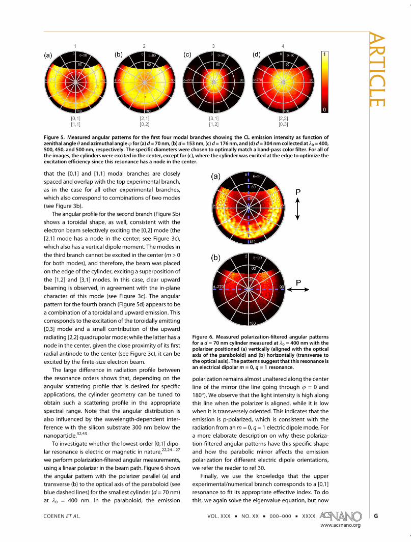
Figure 5 shows the measured radiation patterns forfour different cylinders measured on different reso-nance branches in Figure 3b. The pattern stronglydepends on the resonance mode order. For the smallestcylinder (Figure 5a), which has a resonance lying on thetop experimental branch in Figure 3b, we observea toroidal “doughnut-like” emission pattern at λ0 =400 nm, which has no light emission along thenormal.29,41�43 This pattern corresponds to that of avertically oriented dipole [0,1] mode, which directlyproves that the top measured branch corresponds tothe [0,1] branch. Note that the [1,1] mode is not excitedin the angular CL experiment as the cylinders areexcited in the center, where the [1,1] mode has a node(see Figure 3c). We explain the large discrepancybetween the experimentally observed top branchand the analytically calculated [0,1] mode by the factthat the analytical waveguide model breaks downwhen the diameter is small compared to the wave-length. With the experimental data for the top branchin Figure 3b, identified as the [0,1] mode, we conclude
ARTIC
LE
COENEN ET AL. VOL. XXX ’ NO. XX ’ 000–000 ’ XXXX
www.acsnano.org
G
that the [0,1] and [1,1] modal branches are closelyspaced and overlap with the top experimental branch,as in the case for all other experimental branches,which also correspond to combinations of two modes(see Figure 3b).
The angular profile for the second branch (Figure 5b)shows a toroidal shape, as well, consistent with theelectron beam selectively exciting the [0,2] mode (the[2,1] mode has a node in the center; see Figure 3c),which also has a vertical dipole moment. Themodes inthe third branch cannot be excited in the center (m > 0for both modes), and therefore, the beam was placedon the edge of the cylinder, exciting a superposition ofthe [1,2] and [3,1] modes. In this case, clear upwardbeaming is observed, in agreement with the in-planecharacter of this mode (see Figure 3c). The angularpattern for the fourth branch (Figure 5d) appears to bea combination of a toroidal and upward emission. Thiscorresponds to the excitation of the toroidally emitting[0,3] mode and a small contribution of the upwardradiating [2,2] quadrupolar mode; while the latter has anode in the center, given the close proximity of its firstradial antinode to the center (see Figure 3c), it can beexcited by the finite-size electron beam.
The large difference in radiation profile betweenthe resonance orders shows that, depending on theangular scattering profile that is desired for specificapplications, the cylinder geometry can be tuned toobtain such a scattering profile in the appropriatespectral range. Note that the angular distribution isalso influenced by the wavelength-dependent inter-ference with the silicon substrate 300 nm below thenanoparticle.32,43
To investigate whether the lowest-order [0,1] dipo-lar resonance is electric or magnetic in nature,22,24�27
we perform polarization-filtered angular measurements,using a linear polarizer in the beam path. Figure 6 showsthe angular pattern with the polarizer parallel (a) andtransverse (b) to the optical axis of the paraboloid (seeblue dashed lines) for the smallest cylinder (d = 70 nm)at λ0 = 400 nm. In the paraboloid, the emission
polarization remains almost unaltered along the centerline of the mirror (the line going through j = 0 and180�). We observe that the light intensity is high alongthis line when the polarizer is aligned, while it is lowwhen it is transversely oriented. This indicates that theemission is p-polarized, which is consistent with theradiation from anm = 0, q = 1 electric dipole mode. Fora more elaborate description on why these polariza-tion-filtered angular patterns have this specific shapeand how the parabolic mirror affects the emissionpolarization for different electric dipole orientations,we refer the reader to ref 30.
Finally, we use the knowledge that the upperexperimental/numerical branch corresponds to a [0,1]resonance to fit its appropriate effective index. To dothis, we again solve the eigenvalue equation, but now
Figure 6. Measured polarization-filtered angular patternsfor a d = 70 nm cylinder measured at λ0 = 400 nm with thepolarizer positioned (a) vertically (aligned with the opticalaxis of the paraboloid) and (b) horizontally (transverse tothe optical axis). The patterns suggest that this resonance isan electrical dipolar m = 0, q = 1 resonance.
Figure 5. Measured angular patterns for the first four modal branches showing the CL emission intensity as function ofzenithal angleθ and azimuthal anglej for (a) d=70 nm, (b)d=153nm, (c) d=176nm, and (d) d=304nmcollected at λ0 = 400,500, 450, and 500 nm, respectively. The specific diameters were chosen to optimally match a band-pass color filter. For all ofthe images, the cylinders were excited in the center, except for (c), where the cylinder was excited at the edge to optimize theexcitation efficiency since this resonance has a node in the center.
ARTIC
LE

COENEN ET AL. VOL. XXX ’ NO. XX ’ 000–000 ’ XXXX
www.acsnano.org
H
we fix the resonance wavelength to the resonancewavelengths obtained for the top branch from numer-ical modeling and solve for nc, given that m = 0 andq= 1. In this way, we force the [0,1] branch of themodelto match the experimental data and use this to obtainthe effective index of the cylinder. The resulting indexis shown as an orange line in Figure 4b and is indeedsignificantly lower than the TM0 index that was origin-ally used and gives rise to a significant blue shift ofthe resonance wavelength. The fitted index steadilydecreases with increasing wavelength from n = 2.0 atλ0 = 400 nm to n < 1 for λ0 > 620 nm. This implies thatthe lowest-order resonance approaches cutoff andbecomes a leaky mode that no longer strongly con-fines light inside the cavity. Close observation ofFigure 3b shows that both the experimental andsimulation data of the top resonance branch fade awayaround this wavelength, in agreement with this cutoffargument.We note that the decrease in effectivemodeindex for the cutoff mode with increasing wavelengthis due to both the reduced confinement and the lowerindex of bulk silicon at larger wavelengths. The strongreduction in Q for the [0,1] mode with increasingdiameter is also clearly visible in Figure 3a.
CONCLUSION
In conclusion, the resonant optical modes of siliconnanocylinders with diameters between 60 and 325 nmcan be excited and studied using a 30 keV electronbeam. Well-defined fundamental and higher-orderazimuthal (m = 0�4) and radial (q = 1�4) modes areobserved with relatively narrow (Q = 9�77) emission
peaks and complex photonic wave functions. The dataagree with finite-difference time-domain simulationsand analytical calculations, in which we solve theHelmholtz wave equation using an effective modalindex for the corresponding TM0 waveguide mode tofind the in-plane eigenmodes. Characteristic angularemission patterns are observed for each resonantmode, ranging from an upward dipole-like patternfor the lowest-order modes to distributions that showclear beaming in the upward direction for higher-ordermodes. Using polarization spectroscopy, we identifythe lowest-order resonance as an (m = 0, q = 1)electrical dipole mode; it becomes leaky for longwavelengths.Our measurements demonstrate that the optical
properties of silicon nanocylinders are highly tunablethrough the visible spectral range. Further tunabilitymay be achieved by varying the nanoparticle shape.With the fundamental resonant optical properties ofsingle Si Mie resonators now determined, the door isopen to studies of more complex geometries of arraysof coupled resonators, in which the directionality andspectra of emitted light can be tuned further. This workalso shows that cathodoluminescence spectroscopy,which so far has been usedmostly on resonantmetallicnanostructures, can be used to study the fundamentalresonant properties of single dielectric or semiconduc-tor nanostructures in great detail. In the future, thisenables rapid prototyping of semiconductor or dielec-tric nanostructures, where the spectral and angularemission properties can be fine-tuned for specificapplications.
METHODSFabrication. Small chips (12� 12mm) of SOI wafer (100 nm Si
device layer, 300 nmSiO2 buried oxide layer) are baked for 5minat 180 �C before spin coating the sample with a thin HMDSadhesion layer (4000 rpm, 30 s). The HMDS layer is baked for1 min at 180 �C to evaporate the solvents. Next, the sample isspin coated with approximately 65 nm of negative tone resist(ma-N 2401, 2000 rpm, 30 s) and baked for 60 s at 90 �C. Aucolloids with a diameter of 50 nm are deposited in the corner ofthe sample to allow accurate focusing of the electron beam.
Electron beam lithography is performed in a Raith e-LINEsystem, using a 30 kV acceleration voltage and 7.5 μm aperture,resulting in a beam current of 14 pA. Single dot exposure is usedfor the smallest cylinders (d< 240 nm), whereas area exposure isused for the larger cylinders (d > 270 nm). The resist is devel-oped by rinsing in ma-D 332 S for 15 s, followed by rinsing indeionized H2O to stop the development.
The resulting disks of resist function as an etch mask in thereactive ion etching (RIE) step. A gas mixture of CHF3 (35 sccm)and SF6 (5 sccm) is used to anisotropically etch down the Si layerof the SOI wafer (100 nm) in 3.5 min (forward power = 125 W).Subsequently, the residual resist is removed using a 10 minoxygen plasma etch (20 sccm O2, 50 W forward power).
CL Experiment. The CL experiment was performed in a FEIXL-30 SFEG scanning electron microscope with an aluminumparabolic mirror inside. The mirror alignment is performedusing a specially designed piezoelectric positioning system.29
For spectral imaging, the CLwas focused onto a fiber connected
to a spectrometer with a liquid-nitrogen-cooled CCD array.For the angular measurements, the CL beam was projectedonto a 1024� 1024 pixel imaging CCD array. Emission patternswere obtained by mapping the 2D CCD image of the CL beamonto emission angle θ (zenithal angle) and j (azimuthal angle)and correcting for the collected solid angle per CCD pixel.28 Forthe spectral images, 0.3 s integration time per pixel was used ata current of 10 nA. We use a spatial drift correction algorithm tocorrect for the effects of beam and sample drift. The data arecorrected for system response using a measured transitionradiation spectrum fromgold and comparing that to theory,31,44
so that the absolute excitation efficiency is determined perelectron per unit bandwidth. For the angle-resolved measure-ments, we used dwell times between 15 and 30 s depending onwavelength. For the polarization-filtered angular measure-ments, we used an integration time of 60 s. Spectral sensitivitywas achieved by filtering the CL beam with 40 nm band-passcolor filters. In all cases, the background CL signal from thesubstrate was subtracted from the measured data, which in-cludes the transition radiation of the SiO2 layer and Si substrate.To correctly subtract the variable background from the CLsignal, we use a triangular interpolation routine, which inter-polates the background intensity between the four corners(averaged over nine pixels in each corner) of the scan.
FDTD Simulations. The finite-difference time-domain simula-tions are performed using the commercial software packageLumerical FDTD Solutions.34 An 800 nm cubed simulation box isused, with perfectly matching layer (PML) boundary conditions
ARTIC
LE

COENEN ET AL. VOL. XXX ’ NO. XX ’ 000–000 ’ XXXX
www.acsnano.org
I
on all sides. The simulation box ranges from 150 nm into the Sisubstrate to 250 nm above the top of the cylinders. A constant-current broad band (λ0 = 300�900 nm) vertically orientedelectric dipole, positioned at half the height of the cylinder(50 nm), is used as a source. To simulate the spectrum for a givencylinder diameter, the dipole position is varied from the centerto the edge of the cylinder in steps of 5 nm, such that thenumber of simulations N per cylinder is given by N = R/5 þ 1,with R being the particle radius in nanometers. Two-dimen-sional flux box transmission monitors, the top one positioned100 nm above the top interface of the cylinder, the side ones360 nm from the center of the cylinder, monitor the power ofthe light emitted into the upper hemisphere. Note that inter-ference with the Si substrate is taken into account, but thatlight reflected from the SiO2�Si interface under large anglesmay be radiated into the upper hemisphere without beingdetected. Automatic non-uniform meshing is used, resultingin mesh sizes ranging from 4 to 7 nm in the Si cylinder or air,respectively.
Conflict of Interest: The authors declare no competingfinancial interest.
Acknowledgment. We would like to acknowledge FemiusKoenderink for useful discussions, and Sander Mann, ErikGarnett, and Benjamin Brenny for careful reading of the manu-script. This work is part of the research program of the “Stichtingvoor Fundamenteel Onderzoek der Materie (FOM)”, which isfinancially supported by the “Nederlandse Organisatie voorWetenschappelijk Onderzoek (NWO)”. This work was fundedby an ERC Advanced Investigator Grant and is also part ofNanoNextNL, a nanotechnology program funded by the Dutchministry of economic affairs.
REFERENCES AND NOTES1. Bohren, C. F.; Huffman, D. R. Absorption and Scattering of
Light by Small Particles; JohnWiley & Sons: NewYork, 1983.2. Schuller, A. J.; Brongersma, M. L. General Properties of
Dielectric Optical Antennas. Opt. Express 2009, 17, 24084–24095.
3. Sainidou, R.; Renger, J.; Teperik, T. V.; González, M. U.;Quidant, R.; García de Abajo, F. J. Extraordinary All-Di-electric Light Enhancement over Large Volumes. NanoLett. 2010, 10, 4450–4455.
4. Grzela, G.; Hourlier, D.; Gómez Rivas, J. Polarization-Dependent Light Extinction in Ensembles of PolydisperseVertical Semiconductor Nanowires: A Mie Scattering Ef-fective Medium. Phys. Rev. B 2012, 86, 045305.
5. Spinelli, P.; Verschuuren, M. A.; Polman, A. BroadbandOmnidirectional Antireflection Coating Based on Sub-wavelength Surface Mie Resonators. Nat. Commun. 2012,3, 692.
6. Kelzenberg, M. D.; Boettcher, S. W.; Petykiewicz, J. A.; Turner-Evans, D. B.; Putnam, M. C.; Warren, E. L.; Spurgeon, J. M.;Briggs, R. M.; Lewis, N. S.; Atwater, H. A. Enhanced absorptionand carrier collection in Si wire arrays for photovoltaicapplications. Nat. Mat. 2010, 9, 239�244.
7. Grandidier, J.; Callahan, D. M.; Munday, J. N.; Atwater, H. A.Light Absorption Enhancement in Thin-Film Solar CellsUsing Whispering Gallery Modes in Dielectric Nano-spheres. Adv. Mater. 2011, 23, 1272–1276.
8. Raman, A.; Yu, Z.; Fan, S. Dielectric Nanostructures forBroadband Light Trapping in Organic Solar Cells. Opt.Express 2011, 19, 19015–19026.
9. Mann, S.; Grote, R. R.; Osgood, R. M.; Schuller, J. A. DielectricParticle and Void Resonators for Thin Film Solar CellTextures. Opt. Express 2011, 19, 25729–25740.
10. Kim, S.; Day, R. W.; Cahoon, J. F.; Kempa, T. J.; Song, K.; Park,H.; Lieber, C. M. Tuning Light Absorption in Core/ShellSilicon Nanowire Photovoltaic Devices through Morpho-logical Design. Nano Lett. 2012, 12, 4971–4976.
11. Yu, Y.; Ferry, V. E.; Alivisatos, A. P.; Cao, L. Dielectric Core�Shell Optical Antennas for Strong Solar Absorption En-hancement. Nano Lett. 2012, 12, 3674–3681.
12. Yao, Y.; Yao, J.; Narasimhan, V. K.; Ruan, Z.; Xie, C.; Fan, S.;Cui, Y. Broadband Light Management Using Low-Q Whis-pering Gallery Modes in Spherical Nanoshells. Nat. Com-mun. 2012, 3, 664.
13. Vasudev, A. P.; Schuller, A. J.; Brongersma, M. L. Nano-photonic Light Trapping with Patterned Transparent Con-ductive Oxides. Opt. Express 2012, 20, A385–A394.
14. Tang, J.; Huo, Z.; Brittman, S.; Gao, H.; Yang, P. Solution-Processed Core�Shell Nanowires for Efficient Photovol-taic Cells. Nat. Nanotechnol. 2011, 6, 568–572.
15. van de Molen, K. L.; Zijlstra, P.; Lagendijk, A.; Mosk, A. P.Laser Threshold of Mie Resonances. Opt. Lett. 2006, 31,1432–1434.
16. Cao, L.; White, J. S.; Park, J. S.; Schuller, J. A.; Clemens, B. M.;Brongersma, M. L. Engineering Light Absorption in Semi-conductor Nanowire Devices. Nat. Mater. 2009, 8, 643–647.
17. Cao, L.; Park, J.; Fan, P.; Clemens, B.; Brongersma, M. L.Resonant Germanium Nanoantenna Photodetectors.Nano Lett. 2010, 10, 1229–1233.
18. Alù, A.; Engheta, N. Cloaking a Sensor. Phys. Rev. Lett. 2009,102, 233901.
19. Fan, P.; Chettiar, U. K.; Cao, L.; Afshinmanesh, F.; Engheta,N.; Brongersma, M. L. An Invisible Metal-SemiconductorPhotodetector. Nat. Photonics 2012, 6, 380–385.
20. Yan, R.; Park, J.; Choi, Y.; Heo, C.; Yang, S.; Lee, L. P.; Yang, P.Nanowire-Based Single-Cell Endoscopy.Nat. Nanotechnol.2011, 7, 191–196.
21. Kippenberg, T. J.; Vahala, K. J. Cavity Opto-Mechanics. InPractical Applications of Microresonators in Optics andPhotonics; CRC Press: Boca Raton, FL, 2009.
22. García-Etxarri, A.; Gómez-Medina, R.; Froufe-Pérez, L. S.;López, C.; Chantada, L.; Scheffold, F.; Aizpurua, J.; Nieto-Vesperinas, M.; Sáenz, J. J. Strong Magnetic Response ofSubmicron Silicon Particles in the Infrared. Opt. Express2011, 6, 4815–4826.
23. Zhao, Q.; Kang, L.; Du, B.; Zhao, H.; Xie, Q.; Huang, X.; Li, B.;Zhou, J.; Li, L. Experimental Demonstration of IsotropicNegative Permeability in a Three-Dimensional DielectricComposite. Phys. Rev. Lett. 2008, 101, 027402.
24. Zhao, Q.; Zhou, J.; Zhang, F.; Lippens, D. Mie Resonance-Based Dielectric Metamaterials. Mater. Today 2009, 12,60–69.
25. Evlyukhin, A. B.; Novikov, S. M.; Zywietz, U.; Eriksen, R. L.;Reinhardt, C.; Bozhevolnyi, S. I.; Chichkov, B. N. Demonstra-tion of Magnetic Dipole Resonances of Dielectric Nano-spheres in the Visible Region. Nano Lett. 2012, 12, 3749–3755.
26. Schmidt, M. K.; Esteban, R.; Sáenz, J. J.; Suárez-Lacalle, I.;Mackowski, S.; Aizpurua, J. Dielectric Antennas;A Suita-ble Platform for Controlling Magnetic Dipolar Emission.Opt. Express 2012, 20, 13636–13650.
27. Kuznetsov, A. I.; Miroshnichenko, A. E.; Fu, Y. H.; Zhang, J. B.;Luk'yanchuk, B. Magnetic Light. Sci. Rep. 2012, 2, 492.
28. Coenen, T.; Vesseur, E. J. R.; Polman, A. Angle-ResolvedCathodoluminescence Spectroscopy. Appl. Phys. Lett. 2011,99, 143103.
29. Coenen, T.; Vesseur, E. J. R.; Polman, A.; Koenderink, A. F.Directional Emission from Plasmonic Yagi-Uda AntennasProbed by Angle-Resolved Cathodoluminescence Spec-troscopy. Nano Lett. 2011, 11, 3779–3784.
30. Coenen, T.; Polman, A. Polarization-Sensitive Cathodolu-minescence Fourier Microscopy. Opt. Express 2012, 20,18679–19691.
31. García de Abajo, F. J. Optical Excitations in ElectronMicroscopy. Rev. Mod. Phys. 2010, 82, 209–275.
32. Sapienza, R.; Coenen, T.; Renger, J.; Kuttge, M.; van Hulst,N. F.; Polman, A. Deep-Subwavelength Imaging of theModal Dispersion of Light. Nat. Mater. 2012, 11, 781–787.
33. Stevens-Kalceff, M. A. Cathodoluminescence Microchar-acterization of the Defect Structure of Irradiated Hydratedand Anhydrous Fused Silicon Dioxide. Phys. Rev. B 1998,57, 5674–5683.
34. FDTD Solutions; Lumerical Solutions, Inc.: Vancouver, BC,Canada; www.lumerical.com.
ARTIC
LE

COENEN ET AL. VOL. XXX ’ NO. XX ’ 000–000 ’ XXXX
www.acsnano.org
J
35. Palik, E. D. Handbook of Optical Constants of Solids; Aca-demic: New York, 1985.
36. Jackson, J. D. Classical Electrodynamics; JohnWiley & Sons:Hoboken, NJ, 1999.
37. Snyder, A. W.; Love, J. D. Optical Waveguide Theory; Chap-man & Hall: London, 1996.
38. Slusher, R. E.; Levi, A. F. J.; Mohideen, U.; McCall, S. L.;Pearton, S. J.; Logan, R. A. Threshold Characteristics ofSemiconductor Microdisk Lasers. Appl. Phys. Lett. 1993, 63,1310–1312.
39. Kuttge, M.; García de Abajo, F. J.; Polman, A. UltrasmallMode Volume Plasmonic Nanodisk Resonators. Nano Lett.2010, 10, 1537–1541.
40. Yu, Y.; Cao, L. Coupled Leaky Mode Theory for LightAbsorption in 2D, 1D and 0D Semiconductor Nano-structures. Opt. Express 2012, 20, 13847–13856.
41. Yamamoto, N.; Ohtani, S.; García de Abajo, F. J. Gap andMie Plasmons in Individual Silver Nanospheres near aSilver Surface. Nano Lett. 2011, 11, 91–95.
42. Vesseur, E. J. R.; Polman, A. Plasmonic Whispering GalleryCavities as Optical Nanoantennas. Nano Lett. 2011, 11,5524–5530.
43. Novotny, L.; Hecht, B. Principles of Nano-Optics; CambridgeUniversity Press: New York, 2006.
44. Kuttge, M.; Vesseur, E. J. R.; Koenderink, A. F.; Lezec, H. J.;Atwater, H. A.; García de Abajo, F. J.; Polman, A. LocalDensity of States, Spectrum, and Far-Field Interference ofSurface Plasmon Polaritons Probed by Cathodolumines-cence. Phys. Rev. B 2009, 79, 113405.
ARTIC
LE