quick start guide to vhdl - unisel
TRANSCRIPT
Quick StartGuide to VHDL
Brock J. LaMeres

QUICK START GUIDE TO VHDL
QUICK START GUIDE TO VHDL1ST EDITION
Brock J. LaMeres

Brock J. LaMeresDepartment of Electrical & Computer EngineeringMontana State UniversityBozeman, MT, USA
ISBN 978-3-030-04515-9 ISBN 978-3-030-04516-6 (eBook)https://doi.org/10.1007/978-3-030-04516-6
Library of Congress Control Number: 2018963722
# Springer Nature Switzerland AG 2019This work is subject to copyright. All rights are reserved by the Publisher, whether the whole or part of the material isconcerned, specifically the rights of translation, reprinting, reuse of illustrations, recitation, broadcasting, reproductionon microfilms or in any other physical way, and transmission or information storage and retrieval, electronicadaptation, computer software, or by similar or dissimilar methodology now known or hereafter developed.The use of general descriptive names, registered names, trademarks, service marks, etc. in this publication does notimply, even in the absence of a specific statement, that such names are exempt from the relevant protective laws andregulations and therefore free for general use.The publisher, the authors, and the editors are safe to assume that the advice and information in this book are believedto be true and accurate at the date of publication. Neither the publisher nor the authors or the editors give a warranty,express or implied, with respect to the material contained herein or for any errors or omissions that may have beenmade. The publisher remains neutral with regard to jurisdictional claims in published maps and institutional affiliations.
Cover illustration:# Carloscastilla j Dreamstime.com - Binary Code Photo
This Springer imprint is published by the registered company Springer Nature Switzerland AGThe registered company address is: Gewerbestrasse 11, 6330 Cham, Switzerland
PrefaceThe classical digital design approach (i.e., manual synthesis and minimization of logic) quickly
becomes impractical as systems become more complex. This is the motivation for the modern digital
design flow, which uses hardware description languages (HDL) and computer-aided synthesis/minimi-
zation to create the final circuitry. The purpose of this book is to provide a quick start guide to the VHDL
language, which is one of the two most common languages used to describe logic in the modern digital
design flow. This book is intended for anyone that has already learned the classical digital design
approach and is ready to begin learning HDL-based design. This book is also suitable for practicing
engineers that already know VHDL and need quick reference for syntax and examples of common
circuits. This book assumes that the reader already understands digital logic (i.e., binary numbers,
combinational and sequential logic design, finite state machines, memory, and binary arithmetic basics).
Since this book is designed to accommodate a designer that is new to VHDL, the language is
presented in a manner that builds foundational knowledge first before moving into more complex topics.
As such, Chaps. 1–5 only present functionality built into the VHDL standard package. Only after a
comprehensive explanation of the most commonly used packages from the IEEE library is presented in
Chap. 7, are examples presented that use data types from the widely adopted STD_LOGIC_1164
package. For a reader that is using the book as a reference guide, it may be more practical to pull
examples from Chaps. 7–12 as they use the types std_logic and std_logic_vector. For a VHDL novice,
understanding the history and fundamentals of the VHDL base release will help form a comprehensive
understanding of the language; thus it is recommended that the early chapters are covered in the
sequence they are written.
Bozeman, MT, USA Brock J. LaMeres
v

Acknowledgments
For Alexis. The world is a better place because you are in it.
vii
Contents1: THE MODERN DIGITAL DESIGN FLOW ............................................................. 1
1.1 HISTORY OF HARDWARE DESCRIPTION LANGUAGES ..................................................... 1
1.2 HDL ABSTRACTION ................................................................................................ 4
1.3 THE MODERN DIGITAL DESIGN FLOW ........................................................................ 8
2: VHDL CONSTRUCTS .......................................................................................... 13
2.1 DATA TYPES .......................................................................................................... 13
2.1.1 Enumerated Types ...................................................................................... 13
2.1.2 Range Types ............................................................................................... 14
2.1.3 Physical Types ............................................................................................ 14
2.1.4 Vector Types ................................................................................................ 14
2.1.5 User-Defined Enumerated Types ................................................................ 15
2.1.6 Array Type ................................................................................................... 15
2.1.7 Subtypes ..................................................................................................... 15
2.2 VHDL MODEL CONSTRUCTION ................................................................................ 16
2.2.1 Libraries and Packages .............................................................................. 16
2.2.2 The Entity .................................................................................................... 17
2.2.3 The Architecture .......................................................................................... 17
3: MODELING CONCURRENT FUNCTIONALITY .................................................. 21
3.1 VHDL OPERATORS ................................................................................................ 21
3.1.1 Assignment Operator .................................................................................. 21
3.1.2 Logical Operators ........................................................................................ 22
3.1.3 Numerical Operators ................................................................................... 23
3.1.4 Relational Operators ................................................................................... 23
3.1.5 Shift Operators ............................................................................................ 23
3.1.6 Concatenation Operator .............................................................................. 24
3.2 CONCURRENT SIGNAL ASSIGNMENTS WITH LOGICAL OPERATORS ................................... 24
3.2.1 Logical Operator Example: SOP Circuit ..................................................... 25
3.2.2 Logical Operator Example: One-Hot Decoder ............................................ 26
3.2.3 Logical Operator Example: 7-Segment Display Decoder ........................... 27
3.2.4 Logical Operator Example: One-Hot Encoder ............................................ 29
3.2.5 Logical Operator Example: Multiplexer ....................................................... 31
3.2.6 Logical Operator Example: Demultiplexer .................................................. 32
3.3 CONDITIONAL SIGNAL ASSIGNMENTS .......................................................................... 34
3.3.1 Conditional Signal Assignment Example: SOP Circuit ............................... 34
3.3.2 Conditional Signal Assignment Example: One-Hot Decoder ..................... 35
3.3.3 Conditional Signal Assignment Example: 7-Segment Display Decoder .... 36
3.3.4 Conditional Signal Assignment Example: One-Hot Encoder ..................... 37
3.3.5 Conditional Signal Assignment Example: Multiplexer ................................ 38
3.3.6 Conditional Signal Assignment Example: Demultiplexer ........................... 39
ix
3.4 SELECTED SIGNAL ASSIGNMENTS ............................................................................. 41
3.4.1 Selected Signal Assignment Example: SOP Circuit ................................... 41
3.4.2 Selected Signal Assignment Example: One-Hot Decoder ......................... 42
3.4.3 Selected Signal Assignment Example: 7-Segment Display Decoder ........ 43
3.4.4 Selected Signal Assignment Example: One-Hot Encoder ......................... 44
3.4.5 Selected Signal Assignment Example: Multiplexer .................................... 45
3.4.6 Selected Signal Assignment Example: Demultiplexer ............................... 46
3.5 DELAYED SIGNAL ASSIGNMENTS ............................................................................... 48
3.5.1 Inertial Delay ............................................................................................... 48
3.5.2 Transport Delay ........................................................................................... 48
4: STRUCTURAL DESIGN AND HIERARCHY ........................................................ 53
4.1 COMPONENTS ........................................................................................................ 53
4.1.1 Component Instantiation ............................................................................. 53
4.1.2 Port Mapping ............................................................................................... 53
4.2 STRUCTURAL DESIGN EXAMPLES: RIPPLE CARRY ADDER ............................................. 56
4.2.1 Half Adders .................................................................................................. 56
4.2.2 Full Adders .................................................................................................. 56
4.2.3 Ripple Carry Adder (RCA) .......................................................................... 58
4.2.4 Structural Model of a Ripple Carry Adder in VHDL .................................... 59
5: MODELING SEQUENTIAL FUNCTIONALITY ..................................................... 65
5.1 THE PROCESS ....................................................................................................... 65
5.1.1 Sensitivity Lists ............................................................................................ 65
5.1.2 Wait Statements .......................................................................................... 66
5.1.3 Sequential Signal Assignments .................................................................. 67
5.1.4 Variables ...................................................................................................... 68
5.2 CONDITIONAL PROGRAMMING CONSTRUCTS ................................................................ 70
5.2.1 If/Then Statements ...................................................................................... 70
5.2.2 Case Statements ......................................................................................... 71
5.2.3 Infinite Loops ............................................................................................... 73
5.2.4 While Loops ................................................................................................. 75
5.2.5 For Loops .................................................................................................... 75
5.3 SIGNAL ATTRIBUTES ................................................................................................ 76
6: PACKAGES .......................................................................................................... 81
6.1 STD_LOGIC_1164 ............................................................................................. 81
6.1.1 STD_LOGIC_1164 Resolution Function ..................................................... 82
6.1.2 STD_LOGIC_1164 Logical Operators ........................................................ 83
6.1.3 STD_LOGIC_1164 Edge Detection Functions ........................................... 83
6.1.4 STD_LOGIC_1164 Type Converstion Functions ........................................ 84
6.2 NUMERIC_STD ................................................................................................. 85
6.2.1 NUMERIC_STD Arithmetic Functions ........................................................ 85
6.2.2 NUMERIC_STD Logical Functions ............................................................. 87
6.2.3 NUMERIC_STD Comparison Functions ..................................................... 87
6.2.4 NUMERIC_STD Edge Detection Functions ............................................... 87
x • Contents
6.2.5 NUMERIC_STD Conversion Functions ...................................................... 88
6.2.6 NUMERIC_STD Type Casting .................................................................... 88
6.3 TEXTIO AND STD_LOGIC_TEXTIO ................................................................... 89
6.4 OTHER COMMON PACKAGES .................................................................................... 92
6.4.1 NUMERIC_STD_UNSIGNED ..................................................................... 92
6.4.2 NUMERIC_BIT ............................................................................................ 92
6.4.3 NUMERIC_BIT_UNSIGNED ...................................................................... 93
6.4.4 MATH_REAL ............................................................................................... 93
6.4.5 MATH_COMPLEX ....................................................................................... 95
6.4.6 Legacy Packages (STD_LOGIC_ARITH/UNSIGNED/SIGNED) ............... 95
7: TEST BENCHES .................................................................................................. 99
7.1 TEST BENCH OVERVIEW .......................................................................................... 99
7.2 GENERATING STIMULUS VECTORS USING FOR LOOPS ................................................. 101
7.3 AUTOMATED CHECKING USING REPORT AND ASSERT STATEMENTS ................................ 102
7.3.1 Report Statement ........................................................................................ 102
7.3.2 Assert Statement ......................................................................................... 103
7.4 USING EXTERNAL I/O IN TEST BENCHES ................................................................... 104
7.4.1 Writing to an External File from a Test Bench ............................................ 104
7.4.2 Writing to STD_OUTPUT from a Test Bench ............................................. 107
7.4.3 Reading from an External File in a Test Bench .......................................... 109
7.4.4 Reading Space-Delimited Data from an External File in a Test Bench ..... 111
8: MODELING SEQUENTIAL STORAGE AND REGISTERS ................................. 117
8.1 MODELING SCALAR STORAGE DEVICES ..................................................................... 117
8.1.1 D-Latch ........................................................................................................ 117
8.1.2 D-Flip-Flop ................................................................................................... 118
8.1.3 D-Flip-Flop with Asynchronous Resets ...................................................... 118
8.1.4 D-Flip-Flop with Asynchronous Reset and Preset ...................................... 119
8.1.5 D-Flip-Flop with Synchronous Enable ........................................................ 120
8.2 MODELING REGISTERS ............................................................................................ 121
8.2.1 Registers with Enables ............................................................................... 121
8.2.2 Shift Registers ............................................................................................. 122
8.2.3 Registers as Agents on a Data Bus ............................................................ 123
9: MODELING FINITE STATE MACHINES .............................................................. 127
9.1 THE FSM DESIGN PROCESS AND A PUSH-BUTTON WINDOW CONTROLLER EXAMPLE ...... 127
9.1.1 Modeling the States with User-Defined, Enumerated Data Types ............. 128
9.1.2 The State Memory Process ........................................................................ 129
9.1.3 The Next State Logic Process .................................................................... 129
9.1.4 The Output Logic Process .......................................................................... 130
9.1.5 Explicitly Defining State Codes with Subtypes ........................................... 132
9.2 FSM DESIGN EXAMPLES ........................................................................................ 133
9.2.1 Serial Bit Sequence Detector in VHDL ....................................................... 133
9.2.2 Vending Machine Controller in VHDL ......................................................... 135
9.2.3 2-Bit, Binary Up/Down Counter in VHDL .................................................... 137
Contents • xi
10: MODELING COUNTERS .................................................................................... 143
10.1 MODELING COUNTERS WITH A SINGLE PROCESS ......................................................... 143
10.1.1 Counters in VHDL Using the Type UNSIGNED ......................................... 143
10.1.2 Counters in VHDL Using the Type INTEGER ............................................ 144
10.1.3 Counters in VHDL Using the Type STD_LOGIC_VECTOR ...................... 145
10.2 COUNTERS WITH ENABLES AND LOADS ...................................................................... 148
10.2.1 Modeling Counters with Enables ................................................................ 148
10.2.2 Modeling Counters with Loads ................................................................... 149
11: MODELING MEMORY ........................................................................................ 153
11.1 MEMORY ARCHITECTURE AND TERMINOLOGY .............................................................. 153
11.1.1 Memory Map Model ..................................................................................... 153
11.1.2 Volatile vs. Nonvolatile Memory .................................................................. 154
11.1.3 Read-Only vs. Read/Write Memory ............................................................ 154
11.1.4 Random Access vs. Sequential Access ..................................................... 154
11.2 MODELING READ-ONLY MEMORY .............................................................................. 155
11.3 MODELING READ/WRITE MEMORY ............................................................................ 158
12: COMPUTER SYSTEM DESIGN ......................................................................... 163
12.1 COMPUTER HARDWARE ........................................................................................... 163
12.1.1 Program Memory ........................................................................................ 164
12.1.2 Data Memory ............................................................................................... 164
12.1.3 Input/Output Ports ....................................................................................... 164
12.1.4 Central Processing Unit .............................................................................. 164
12.1.5 A Memory-Mapped System ........................................................................ 166
12.2 COMPUTER SOFTWARE ............................................................................................ 168
12.2.1 Opcodes and Operands .............................................................................. 169
12.2.2 Addressing Modes ...................................................................................... 169
12.2.3 Classes of Instructions ................................................................................ 170
12.3 COMPUTER IMPLEMENTATION: AN 8-BIT COMPUTER EXAMPLE ...................................... 177
12.3.1 Top-Level Block Diagram ............................................................................ 177
12.3.2 Instruction Set Design ................................................................................. 178
12.3.3 Memory System Implementation ................................................................ 179
12.3.4 CPU Implementation ................................................................................... 184
APPENDIX A: LIST OF WORKED EXAMPLES ...................................................... 207
INDEX ....................................................................................................................... 211
xii • Contents
Chapter 1: The Modern Digital
Design FlowThe purpose of a hardware description languages is to describe digital circuitry using a text-based
language. HDLs provide a means to describe large digital systems without the need for schematics,
which can become impractical in very large designs. HDLs have evolved to support logic simulation at
different levels of abstraction. This provides designers the ability to begin designing and verifying
functionality of large systems at a high level of abstraction and postpone the details of the circuit
implementation until later in the design cycle. This enables a top-down design approach that is scalable
across different logic families. HDLs have also evolved to support automated synthesis, which allows the
CAD tools to take a functional description of a system (e.g., a truth table) and automatically create the
gate-level circuitry to be implemented in real hardware. This allows designers to focus their attention on
designing the behavior of a system and not spend as much time performing the formal logic synthesis
steps as in the classical digital design approach. The goal of this chapter is to provide the background
and context of the modern digital design flow using an HDL-based approach.
There are two dominant hardware description languages in use today. They are VHDL and Verilog.
VHDL stands for very high speed integrated circuit hardware description language. Verilog is not an
acronym but rather a trade name. The use of these two HDLs is split nearly equally within the digital
design industry. Once one language is learned, it is simple to learn the other language, so the choice of
the HDL to learn first is somewhat arbitrary. In this text, we will use VHDL to learn the concepts of an
HDL. VHDL is stricter in its syntax and typecasting than Verilog, so it is a good platform for beginners as it
provides more of a scaffold for the description of circuits. This helps avoid some of the common pitfalls
that beginners typically encounter. The goal of this chapter is to provide the background and context of
the modern digital design flow using an HDL-based approach.
Learning Outcomes—After completing this chapter, you will be able to:
1.1 Describe the role of hardware description languages in modern digital design.1.2 Describe the fundamentals of design abstraction in modern digital design.1.3 Describe the modern digital design flow based on hardware description languages.
1.1 History of Hardware Description Languages
The invention of the integrated circuit is most commonly credited to two individuals who filed patents
on different variations of the same basic concept within 6 months of each other in 1959. Jack Kilby filed
the first patent on the integrated circuit in February of 1959 titled “Miniaturized Electronic Circuits” while
working for Texas Instruments. Robert Noyce was the second to file a patent on the integrated circuit in
July of 1959 titled “Semiconductor Device and Lead Structure” while at a company he cofounded called
Fairchild Semiconductor. Kilby went on to win the Nobel Prize in Physics in 2000 for his invention, while
Noyce went on to cofound Intel Corporation in 1968 with Gordon Moore. In 1971, Intel introduced the first
single-chip microprocessor using integrated circuit technology, the Intel 4004. This microprocessor IC
contained 2300 transistors. This series of inventions launched the semiconductor industry, which was
the driving force behind the growth of Silicon Valley, and led to 40 years of unprecedented advancement
in technology that has impacted every aspect of the modern world.
Gordon Moore, cofounder of Intel, predicted in 1965 that the number of transistors on an integrated
circuit would double every 2 years. This prediction, now known as Moore’s Law, has held true since the
# Springer Nature Switzerland AG 2019
B. J. LaMeres, Quick Start Guide to VHDL, https://doi.org/10.1007/978-3-030-04516-6_1
1
invention of the integrated circuit. As the number of transistors on an integrated circuit grew, so did the
size of the design and the functionality that could be implemented. Once the first microprocessor was
invented in 1971, the capability of CAD tools increased rapidly enabling larger designs to be accom-
plished. These larger designs, including newer microprocessors, enabled the CAD tools to become even
more sophisticated and, in turn, yield even larger designs. The rapid expansion of electronic systems
based on digital integrated circuits required that different manufacturers needed to produce designs that
were compatible with each other. The adoption of logic family standards helped manufacturers ensure
their parts would be compatible with other manufacturers at the physical layer (e.g., voltage and current);
however, one challenge that was encountered by the industry was a way to document the complex
behavior of larger systems. The use of schematics to document large digital designs became too
cumbersome and difficult to understand by anyone besides the designer. Word descriptions of the
behavior were easier to understand, but even this form of documentation became too voluminous to
be effective for the size of designs that were emerging.
In 1983, the US Department of Defense (DoD) sponsored a program to create a means to document
the behavior of digital systems that could be used across all of its suppliers. This program was motivated
by a lack of adequate documentation for the functionality of application specific integrated circuits
(ASICs) that were being supplied to the DoD. This lack of documentation was becoming a critical
issue as ASICs would come to the end of their life cycle and need to be replaced. With the lack of a
standardized documentation approach, suppliers had difficulty reproducing equivalent parts to those that
had become obsolete. The DoD contracted three companies (Texas Instruments, IBM, and Intermetrics)
to develop a standardized documentation tool that provided detailed information about both the interface
(i.e., inputs and outputs) and the behavior of digital systems. The new tool was to be implemented in a
format similar to a programming language. Due to the nature of this type of language-based tool, it was a
natural extension of the original project scope to include the ability to simulate the behavior of a digital
system. The simulation capability was desired to span multiple levels of abstraction to provide maximum
flexibility. In 1985, the first version of this tool, called VHDL, was released. In order to gain widespread
adoption and ensure consistency of use across the industry, VHDL was turned over to the Institute of
Electrical and Electronic Engineers (IEEE) for standardization. IEEE is a professional association that
defines a broad range of open technology standards. In 1987, IEEE released the first industry standard
version of VHDL. The release was titled IEEE 1076-1987. Feedback from the initial version resulted in a
major revision of the standard in 1993 titled IEEE 1076-1993. While many minor revisions have been
made to the 1993 release, the 1076-1993 standard contains the vast majority of VHDL functionality in
use today. The most recent VHDL standard is IEEE 1076-2008.
Also in 1983, the Verilog HDL was developed by Automated Integrated Design Systems as a logic
simulation language. The development of Verilog took place completely independent from the VHDL
project. Automated Integrated Design Systems (renamed Gateway Design Automation in 1985) was
acquired by CAD tool vendor Cadence Design Systems in 1990. In response to the rapid adoption of the
open VHDL standard, Cadence made the Verilog HDL open to the public in order to stay competitive.
IEEE once again developed the open standard for this HDL and in 1995 released the Verilog standard
titled IEEE 1364.
The development of CAD tools to accomplish automated logic synthesis can be dated back to the
1970s when IBM began developing a series of practical synthesis engines that were used in the design
of their mainframe computers; however, the main advancement in logic synthesis came with the founding
of a company called Synopsis in 1986. Synopsis was the first company to focus on logic synthesis
directly from HDLs. This was a major contribution because designers were already using HDLs to
describe and simulate their digital systems, and now logic synthesis became integrated in the same
design flow. Due to the complexity of synthesizing highly abstract functional descriptions, only lower
levels of abstraction that were thoroughly elaborated were initially able to be synthesized. As CAD tool
2 • Chapter 1: The Modern Digital Design Flow
capability evolved, synthesis of higher levels of abstraction became possible, but even today not all
functionality that can be described in an HDL can be synthesized.
The history of HDLs, their standardization, and the creation of the associated logic synthesis tools
are key to understanding the use and limitations of HDLs. HDLs were originally designed for documen-
tation and behavioral simulation. Logic synthesis tools were developed independently and modified later
to work with HDLs. This history provides some background into the most common pitfalls that beginning
digital designers encounter, that being that most any type of behavior can be described and simulated in
an HDL, but only a subset of well-described functionality can be synthesized. Beginning digital designers
are often plagued by issues related to designs that simulate perfectly but that will not synthesize
correctly. In this book, an effort is made to introduce VHDL at a level that provides a reasonable amount
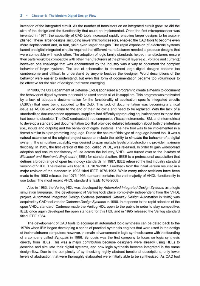
of abstraction while preserving the ability to be synthesized. Figure 1.1 shows a timeline of some of the
major technology milestones that have occurred in the past 150 years in the field of digital logic and
HDLs.
Fig. 1.1Major milestones in the advancement of digital logic and HDLs
1.1 History of Hardware Description Languages • 3
CONCEPT CHECK
CC1.1 Why does VHDL support modeling techniques that aren’t synthesizable?
(A) Since synthesis wasn’t within the original scope of the VHDL project, therewasn’t sufficient time to make everything synthesizable.
(B) At the time VHDL was created, synthesis was deemed too difficult toimplement.
(C) To allow VHDL to be used as a generic programming language.
(D) VHDL needs to support all steps in the modern digital design flow, some ofwhich are unsynthesizable such as test pattern generation and timingverification.
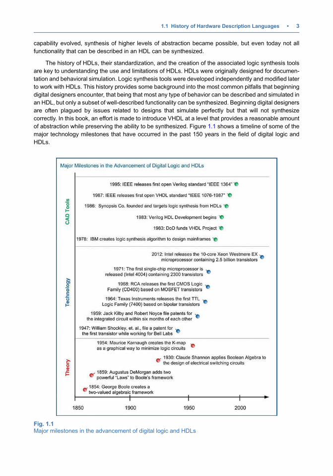
1.2 HDL Abstraction
HDLs were originally defined to be able to model behavior at multiple levels of abstraction.
Abstraction is an important concept in engineering design because it allows us to specify how systems
will operate without getting consumed prematurely with implementation details. Also, by removing the
details of the lower-level implementation, simulations can be conducted in reasonable amounts of time to
model the higher-level functionality. If a full computer system was simulated using detailed models for
every MOSFET, it would take an impracticable amount of time to complete. Figure 1.2 shows a graphical
depiction of the different layers of abstraction in digital system design.
Fig. 1.2Levels of design abstraction
4 • Chapter 1: The Modern Digital Design Flow
The highest level of abstraction is the system level. At this level, behavior of a system is
described by stating a set of broad specifications. An example of a design at this level is a specifica-
tion such as “the computer system will perform 10 Tera Floating Point Operations per Second
(10 TFLOPS) on double precision data and consume no more than 100 W of power.” Notice that
these specifications do not dictate the lower-level details such as the type of logic family or the type of
computer architecture to use. One level down from the system level is the algorithmic level. At this
level, the specifications begin to be broken down into sub-systems, each with an associated behavior
that will accomplish a part of the primary task. At this level, the example computer specifications might
be broken down into sub-systems such as a central processing unit (CPU) to perform the computation
and random access memory (RAM) to hold the inputs and outputs of the computation. One level down
from the algorithmic level is the register-transfer level (RTL). At this level, the details of how data is
moved between and within sub-systems are described in addition to how the data is manipulated
based on system inputs. One level down from the RTL level is the gate level. At this level, the design
is described using basic gates and registers (or storage elements). The gate level is essentially a
schematic (either graphically or text-based) that contains the components and connections that will
implement the functionality from the above levels of abstraction. One level down from the gate level is
the circuit level. The circuit level describes the operation of the basic gates and registers using
transistors, wires, and other electrical components such as resistors and capacitors. Finally, the
lowest level of design abstraction is the material level. This level describes how different materials
are combined and shaped in order to implement the transistors, devices, and wires from the circuit
level.
HDLs are designed to model behavior at all of these levels with the exception of the material level.
While there is some capability to model circuit-level behavior such as MOSFETs as ideal switches and
pull-up/pull-down resistors, HDLs are not typically used at the circuit level. Another graphical depiction of
design abstraction is known as Gajski and Kuhn’s Y-chart. A Y-chart depicts abstraction across three
different design domains: behavioral, structural, and physical. Each of these design domains contains
levels of abstraction (i.e., system, algorithm, RTL, gate, and circuit). An example Y-chart is shown in
Fig. 1.3.
1.2 HDL Abstraction • 5
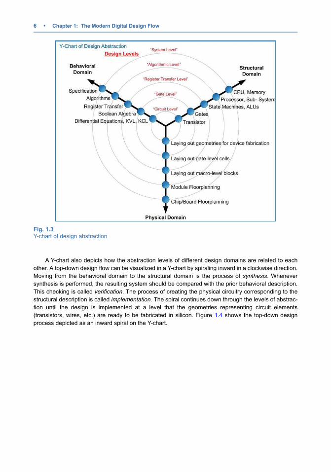
A Y-chart also depicts how the abstraction levels of different design domains are related to each
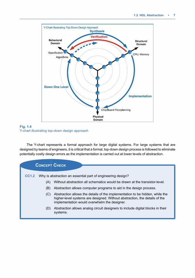
other. A top-down design flow can be visualized in a Y-chart by spiraling inward in a clockwise direction.
Moving from the behavioral domain to the structural domain is the process of synthesis. Whenever
synthesis is performed, the resulting system should be compared with the prior behavioral description.
This checking is called verification. The process of creating the physical circuitry corresponding to the
structural description is called implementation. The spiral continues down through the levels of abstrac-
tion until the design is implemented at a level that the geometries representing circuit elements
(transistors, wires, etc.) are ready to be fabricated in silicon. Figure 1.4 shows the top-down design
process depicted as an inward spiral on the Y-chart.
Fig. 1.3Y-chart of design abstraction
6 • Chapter 1: The Modern Digital Design Flow
The Y-chart represents a formal approach for large digital systems. For large systems that are
designed by teams of engineers, it is critical that a formal, top-down design process is followed to eliminate
potentially costly design errors as the implementation is carried out at lower levels of abstraction.
CONCEPT CHECK
CC1.2 Why is abstraction an essential part of engineering design?
(A) Without abstraction all schematics would be drawn at the transistor-level.
(B) Abstraction allows computer programs to aid in the design process.
(C) Abstraction allows the details of the implementation to be hidden, while thehigher-level systems are designed. Without abstraction, the details of theimplementation would overwhelm the designer.
(D) Abstraction allows analog circuit designers to include digital blocks in theirsystems.
Fig. 1.4Y-chart illustrating top-down design approach
1.2 HDL Abstraction • 7
1.3 The Modern Digital Design Flow
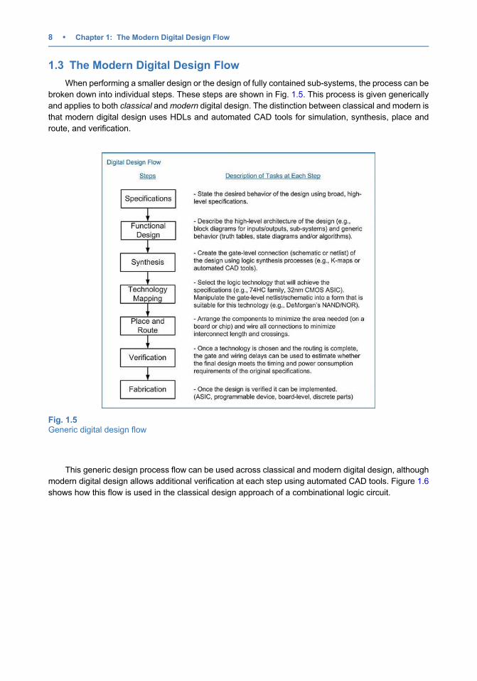
When performing a smaller design or the design of fully contained sub-systems, the process can be
broken down into individual steps. These steps are shown in Fig. 1.5. This process is given generically
and applies to both classical andmodern digital design. The distinction between classical and modern is
that modern digital design uses HDLs and automated CAD tools for simulation, synthesis, place and
route, and verification.
This generic design process flow can be used across classical and modern digital design, although
modern digital design allows additional verification at each step using automated CAD tools. Figure 1.6
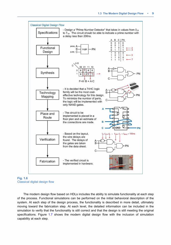
shows how this flow is used in the classical design approach of a combinational logic circuit.
Fig. 1.5Generic digital design flow
8 • Chapter 1: The Modern Digital Design Flow
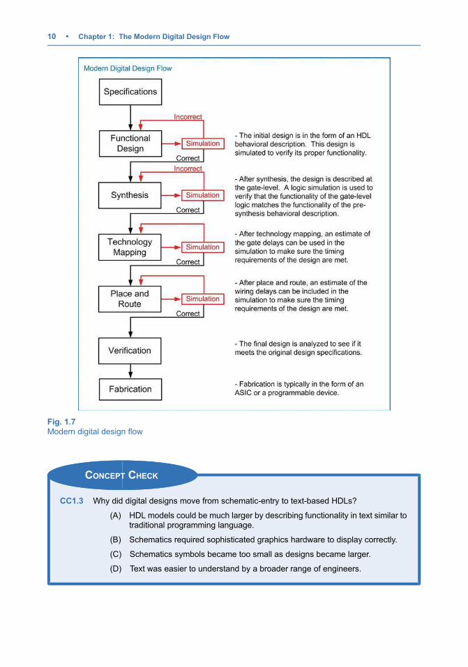
The modern design flow based on HDLs includes the ability to simulate functionality at each step
of the process. Functional simulations can be performed on the initial behavioral description of the
system. At each step of the design process, the functionality is described in more detail, ultimately
moving toward the fabrication step. At each level, the detailed information can be included in the
simulation to verify that the functionality is still correct and that the design is still meeting the original
specifications. Figure 1.7 shows the modern digital design flow with the inclusion of simulation
capability at each step.
Fig. 1.6Classical digital design flow
1.3 The Modern Digital Design Flow • 9
CONCEPT CHECK
CC1.3 Why did digital designs move from schematic-entry to text-based HDLs?
(A) HDL models could be much larger by describing functionality in text similar totraditional programming language.
(B) Schematics required sophisticated graphics hardware to display correctly.
(C) Schematics symbols became too small as designs became larger.
(D) Text was easier to understand by a broader range of engineers.
Fig. 1.7Modern digital design flow
10 • Chapter 1: The Modern Digital Design Flow
Summary
v The modern digital design flow relies oncomputer-aided engineering (CAE) andcomputer-aided design (CAD) tools to man-age the size and complexity of today’s digitaldesigns.
v Hardware description languages (HDLs)allow the functionality of digital systems tobe entered using text. VHDL and Verilog arethe two most common HDLs in use today.
v VHDL was originally created to document thebehavior of large digital systems and supportfunctional simulations.
v The ability to automatically synthesize a logiccircuit from a VHDL behavioral description
became possible approximately 10 yearsafter the original definition of VHDL. Assuch, only a subset of the behavioralmodeling techniques in VHDL can be auto-matically synthesized.
v HDLs can model digital systems at differentlevels of design abstraction. These includethe system, algorithmic, RTL, gate, and cir-cuit levels. Designing at a higher level ofabstraction allows more complex systems tobe modeled without worrying about thedetails of the implementation.
Exercise Problems
Section 1.1: History of HDLs
1.1.1 What was the original purpose of VHDL?
1.1.2 Can all of the functionality that can bedescribed in VHDL be simulated?
1.1.3 Can all of the functionality that can bedescribed in VHDL be synthesized?
Section 1.2: HDL Abstraction
1.2.1 Give the level of design abstraction that thefollowing statement relates to: if there is everan error in the system, it should return to thereset state.
1.2.2 Give the level of design abstraction that thefollowing statement relates to: once the designis implemented in a sum of products form,DeMorgan’s Theorem will be used to convertit to a NAND-gate only implementation.
1.2.3 Give the level of design abstraction that thefollowing statement relates to: the design willbe broken down into two sub-systems, one thatwill handle data collection and the other thatwill control data flow.
1.2.4 Give the level of design abstraction that thefollowing statement relates to: the interconnecton the IC should be changed from aluminum tocopper to achieve the performance needed inthis design.
1.2.5 Give the level of design abstraction that thefollowing statement relates to: the MOSFETsneed to be able to drive at least eight otherloads in this design.
1.2.6 Give the level of design abstraction that thefollowing statement relates to: this system willcontain 1 host computer and support up to1000 client computers.
1.2.7 Give the design domain that the following activ-ity relates to: drawing the physical layout of theCPU will require 6 months of engineering time.
1.2.8 Give the design domain that the following activ-ity relates to: the CPU will be connected to fourbanks of memory.
1.2.9 Give the design domain that the following activ-ity relates to: the fan-in specifications for thislogic family require excessive logic circuitry tobe used.
1.2.10 Give the design domain that the following activ-ity relates to: the performance specificationsfor this system require 1 TFLOP at <5 W.
Section 1.3: The Modern Digital Design
Flow
1.3.1 Which step in the modern digital design flowdoes the following statement relate to: a CADtool will convert the behavioral model into agate-level description of functionality.
1.3.2 Which step in the modern digital design flowdoes the following statement relate to: afterrealistic gate and wiring delays are determined,one last simulation should be performed tomake sure the design meets the original timingrequirements.
1.3.3 Which step in the modern digital designflow does the following statement relate to: ifthe memory is distributed around the perimeterof the CPU, the wiring density will beminimized.
1.3.4 Which step in the modern digital design flowdoes the following statement relate to: thedesign meets all requirements so now I’mbuilding the hardware that will be shipped.
Exercise Problems • 11
1.3.5 Which step in the modern digital design flowdoes the following statement relate to: thesystem will be broken down into threesub-systems with the following behaviors.
1.3.6 Which step in the modern digital design flowdoes the following statement relate to: thissystem needs to have 10 GB of memory.
1.3.7 Which step in the modern digital design flowdoes the following statement relate to: to meetthe power requirements, the gates will beimplemented in the 74HC logic family.
12 • Chapter 1: The Modern Digital Design Flow
Chapter 2: VHDL ConstructsThis chapter begins looking at the basic construction of a VHDL model. This chapter begins by
covering the built-in features of a VHDL model including the file structure, data types, operators, and
declarations. This chapter provides a foundation of VHDL that will lead to modeling examples provided in
Chap. 3. VHDL is not case sensitive. Each VHDL assignment, definition, or declaration is terminated with
a semicolon (;). As such, line wraps are allowed and do not signify the end of an assignment, definition, or
declaration. Line wraps can be used to make the VHDL more readable. Comments in VHDL are
preceded with two dashes (i.e., --) and continue until the end of the line. All user-defined names in
VHDL must start with an alphabetic letter, not a number. User-defined names are not allowed to be the
same as any VHDL keyword. This chapter contains many definitions of syntax in VHDL. The following
notations will be used throughout the chapter when introducing new constructs:
bold ¼ VHDL keyword, use as is
italics ¼ User-defined name
<> ¼ A required characteristic such as a data type, input/output, etc.
Learning Outcomes—After completing this chapter, you will be able to:
2.1 Describe the data types provided in the standard VHDL package.2.2 Describe the basic construction of a VHDL model.
2.1 Data Types
In VHDL, every signal, constant, variable, and function must be assigned a data type. The IEEE
standard package provides a variety of pre-defined data types. Some data types are synthesizable,
while others are only for modeling abstract behavior. The following are the most commonly used data
types in the VHDL standard package.
2.1.1 Enumerated Types
An enumerated type is one in which the exact values that the type can take on are defined.
Type Values that the type can take on
bit {0, 1}
boolean {false, true}
character {“any of the 256 ASCII characters defined in ISO 8859-1”}
The type bit is synthesizable, while Boolean and character are not. The individual scalar values are
indicated by putting them inside single quotes (e.g., ‘0,’ ‘a,’ ‘true’).
# Springer Nature Switzerland AG 2019
B. J. LaMeres, Quick Start Guide to VHDL, https://doi.org/10.1007/978-3-030-04516-6_2
13
2.1.2 Range Types
A range type is one that can take on any value within a range.
Type Values that the type can take on
integer Whole numbers between �2,147,483,648 and +2,147,483,647
real Fractional numbers between �1.7e38 and +1.7e38
The integer type is a 32-bit, signed, two’s complement number and is synthesizable. If the full range
of integer values is not desired, this type can be bounded by including range <min> to <max>. The real
type is a 32-bit, floating point value and is not directly synthesizable unless an additional package is
included that defines the floating point format. The values of these types are indicated by simply using
the number without quotes (e.g., 33, 3.14).
2.1.3 Physical Types
A physical type is one that contains both a value and units. In VHDL, time is the primary supported
physical type.
Type Values that the type can take on
time Whole numbers between �2,147,483,648
and +2,147,483,647
(unit relationships) fs (femtosecond, 10�15),
base unit
ps ¼ 1000 fs (picosecond, 10�12)
ns ¼ 1000 ps (nanosecond, 10�9)
μs ¼ 1000 ns (microsecond, 10�6)
ms ¼ 1000 μs (millisecond, 10�3)
s ¼ 1000 ms (second)
min ¼ 60 s (minute)
h ¼ 60 min (hour)
The base unit for time is fs, meaning that, if no units are provided, the value is assumed to be in
femtoseconds. The value of time is held as a 32-bit, signed number and is not synthesizable.
2.1.4 Vector Types
A vector type is one that consists of a linear array of scalar types.
Type Construction
bit_vector A linear array of type bit
string A linear array of type character
The size of a vector type is defined by including the maximum index, the keyword downto, and the
minimum index. For example, if a signal called BUS_A was given the type bit_vector(7 downto 0), it
would create a vector of 8 scalars, each of type bit. The leftmost scalar would have an index of 7 and the
rightmost scalar would have an index of 0. Each of the individual scalars within the vector can be
accessed by providing the index number in parentheses. For example, BUS_A(0) would access the
14 • Chapter 2: VHDL Constructs
scalar in the rightmost position. The indices do not always need to have a minimum value of 0, but this is
the most common indexing approach in logic design. The type bit_vector is synthesizable, while string is
not. The values of these types are indicated by enclosing them inside double quotes (e.g., “0011,” “abcd”).
2.1.5 User-Defined Enumerated Types
A user-defined enumerated type is one in which the name of the type is specified by the user in
addition to all of the possible values that the type can assume. The creation of a user-defined
enumerated type is shown below.
type name is (value1, value2, . . .);
Example:
type traffic_light is (red, yellow, green);
In this example, a new type is created called traffic_light. If we declared a new signal called Sig1 and
assigned it the type traffic_light, the signal could only take on values of red, yellow, and green. User-
defined enumerated types are synthesizable in specific applications.
2.1.6 Array Type
An array contains multiple elements of the same type. Elements within an array can be scalar or
vectors. In order to use an array, a new type must be declared that defines the configuration of the array.
Once the new type is created, signals may be declared of that type. The range of the array must be
defined in the array-type declaration. The range is specified with integers (min and max) and either the
keywords downto or to. The creation of an array type is shown below.
type name is array (<range>) of <element_type>;
Example:
type block_8x16 is array (0 to 7) bit_vector(15 downto 0);
signal my_array : block_8x16;
In this example, the new array type is declared with eight elements. The beginning index of the array
is 0 and the ending index is 7. Each element in the array is a 16-bit vector of type bit_vector.
2.1.7 Subtypes
A subtype is a constrained version or subset of another type. Subtypes are user-defined, although a
few commonly used subtypes are pre-defined in the standard package. The following is the syntax for
declaring a subtype and two examples of commonly used subtypes (NATURAL and POSTIVE) that are
defined in the standard package.
subtype name is <type> range <min> to <max>;
Example:
subtype NATURAL is integer range 0 to 255;
subtype POSTIVE is integer range 1 to 256;
2.1 Data Types • 15
CONCEPT CHECK
CC2.1 What is the difference between types Boolean {TRUE, FALSE} and bit{0, 1}?
(A) They are the same.
(B) Boolean is used for decision-making constructs (when, else), whilebit is used to model real digital signals.
(C) Logical operators work with type Boolean but not for type bit.
(D) Only type bit is synthesizable.
2.2 VHDL Model Construction
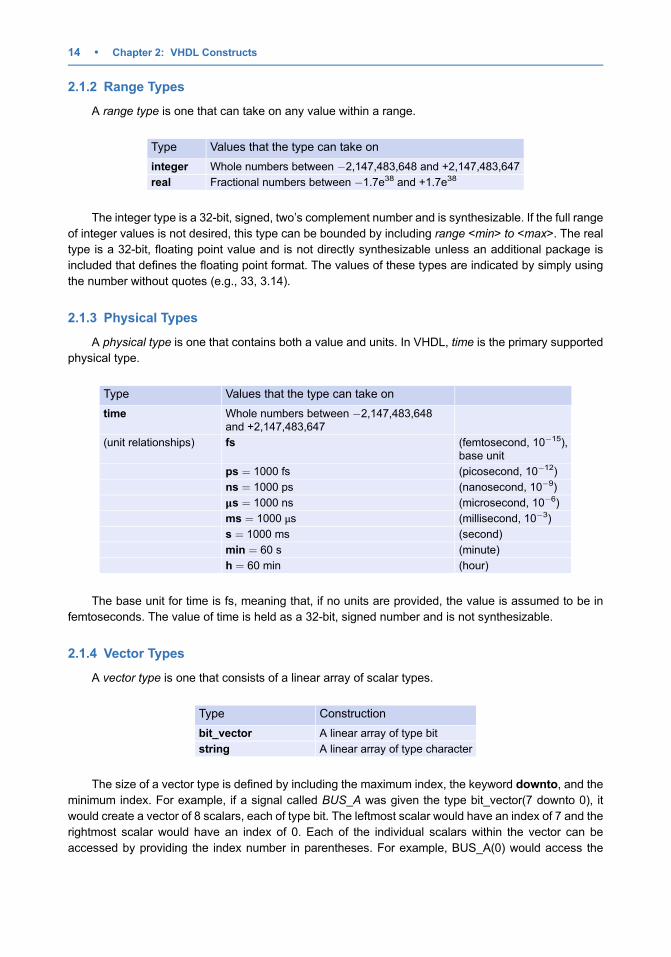
AVHDL design describes a single system in a single file. The file has the suffix *.vhd. Within the file,
there are two parts that describe the system: the entity and the architecture. The entity describes the
interface to the system (i.e., the inputs and outputs) and the architecture describes the behavior. The
functionality of VHDL (e.g., operators, signal types, functions, etc.) is defined in the package. Packages
are grouped within a library. IEEE defines the base set of functionality for VHDL in the standard
package. This package is contained within a library called IEEE. The library and package inclusion is
stated at the beginning of a VHDL file before the entity and architecture. Additional functionality can be
added to VHDL by including other packages, but all packages are based on the core functionality defined
in the standard package. As a result, it is not necessary to explicitly state that a design is using the IEEE
standard package because it is inherent in the use of VHDL. All functionality described in this chapter is
for the IEEE standard package, while other common packages are covered in subsequent chapters.
Figure 2.1 shows a graphical depiction of a VHDL file.
2.2.1 Libraries and Packages
As mentioned earlier, the IEEE standard package is implied when using VHDL; however, we can
use it as an example of how to include packages in VHDL. The keyword library is used to signify that
packages are going to be added to the VHDL design from the specified library. The name of the library
Fig. 2.1The anatomy of a VHDL file
16 • Chapter 2: VHDL Constructs
follows this keyword. To include a specific package from the library, a new line is used with the keyword
use followed by the package details. The package syntax has three fields separated with a period. The
first field is the library name. The second field is the package name. The third field is the specific
functionality of the package to be included. If all functionality of a package is to be used, then the
keyword all is used in the third field. Examples of how to include some of the commonly used packages
from the IEEE library are shown below.
library IEEE;
use IEEE.std_logic_1164.all;
use IEEE.numeric_std.all;
use IEEE.std_logic_textio.all;
2.2.2 The Entity
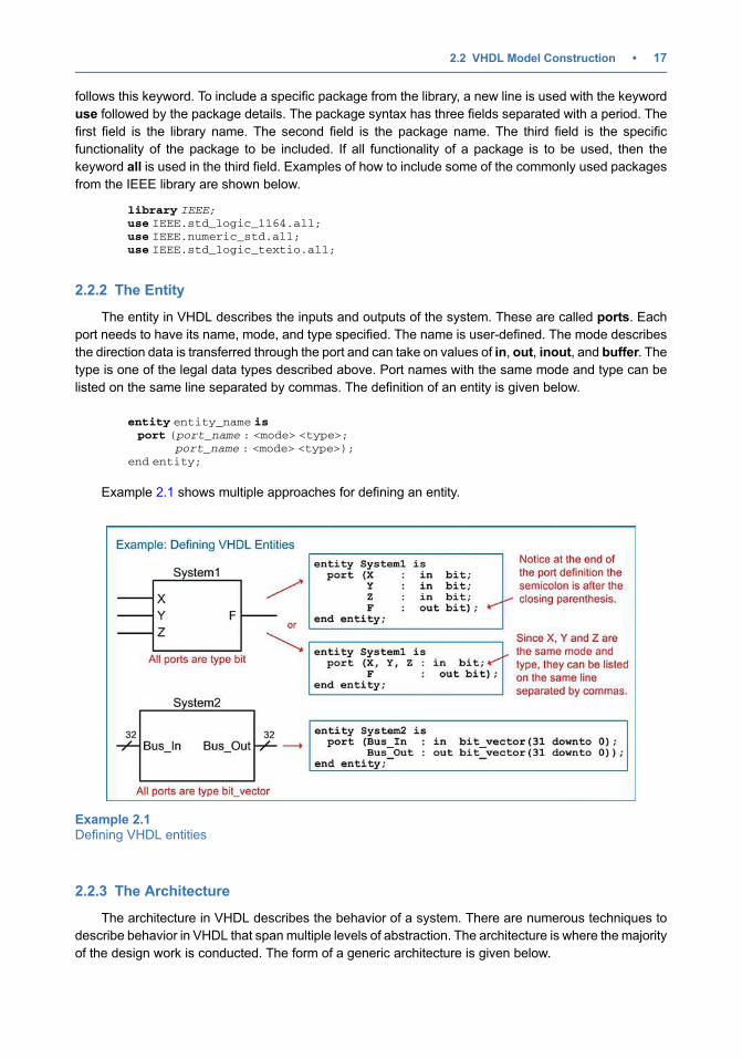
The entity in VHDL describes the inputs and outputs of the system. These are called ports. Each
port needs to have its name, mode, and type specified. The name is user-defined. The mode describes
the direction data is transferred through the port and can take on values of in, out, inout, and buffer. The
type is one of the legal data types described above. Port names with the same mode and type can be
listed on the same line separated by commas. The definition of an entity is given below.
entity entity_name is
port (port_name : <mode> <type>;
port_name : <mode> <type>);
end entity;
Example 2.1 shows multiple approaches for defining an entity.
2.2.3 The Architecture
The architecture in VHDL describes the behavior of a system. There are numerous techniques to
describe behavior in VHDL that span multiple levels of abstraction. The architecture is where the majority
of the design work is conducted. The form of a generic architecture is given below.
Example 2.1Defining VHDL entities
2.2 VHDL Model Construction • 17
architecture architecture_name of <entity associated with> is
-- user-defined enumerated type declarations (optional)
-- signal declarations (optional)
-- constant declarations (optional)
-- component declarations (optional)
begin
-- behavioral description of the system goes here
end architecture;
2.2.3.1 Signal Declarations
A signal that is used for internal connections within a system is declared in the architecture. Each
signal must be declared with a type. The signal can only be used to make connections of like types. A
signal is declared with the keyword signal followed by a user-defined name, colon, and the type. Signals
of like type can be declared on the same line separated with a comma. All of the legal data types
described above can be used for signals. Signals represent wires within the system so they do not have
a direction or mode. Signals cannot have the same name as a port in the system in which they reside.
The syntax for a signal declaration is as follows:
signal name : <type>;
Example:
signal node1 : bit;
signal a1, b1 : integer;
signal Bus3 : bit_vector (15 downto 0);
signal C_int : integer range 0 to 255;
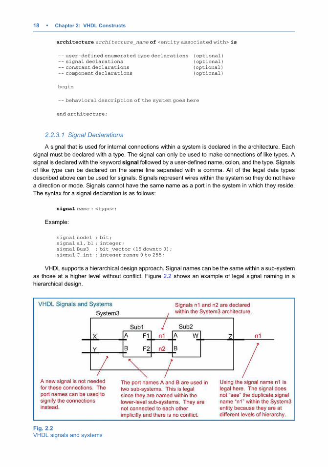
VHDL supports a hierarchical design approach. Signal names can be the same within a sub-system
as those at a higher level without conflict. Figure 2.2 shows an example of legal signal naming in a
hierarchical design.
Fig. 2.2VHDL signals and systems
18 • Chapter 2: VHDL Constructs
2.2.3.2 Constant Declarations
A constant is useful for representing a quantity that will be used multiple times in the architecture.
The syntax for declaring a constant is as follows:
constant constant_name : <type> :¼ <value>;
Example:
constant BUS_WIDTH : integer :¼ 32;
Once declared, the constant name can now be used throughout the architecture. The following
example illustrates how we can use a constant to define the size of a vector. Notice that since we defined
the constant to be the actual width of the vector (i.e., 32-bits), we need to subtract one from its value
when defining the indices (i.e., 31 down to 0).
Example:
signal BUS_A : bit_vector (BUS_WIDTH-1 downto 0);
2.2.3.3 Component Declarations
A component is the term used for a VHDL sub-system that is instantiated within a higher-level
system. If a component is going to be used within a system, it must be declared in the architecture before
the begin statement. The syntax for a component declaration is as follows:
component component_name
port (port_name : <mode> <type>;
port_name : <mode> <type>);
end component;
The port definitions of the component must match the port definitions of the sub-system’s entity
exactly. As such, these lines are typically copied directly from the lower-level systems VHDL entity
description. Once declared, a component can be instantiated after the begin statement in the architec-
ture as many times as needed.
CONCEPT CHECK
CC2.2 Why don’t we need to explicitly include the STANDARD package when creating a VHDLdesign?
(A) It defines the base functionality of VHDL so its use is implied.
(B) The simulator will automatically add it to the .vhd file upon compile.
(C) It isn’t recognized by synthesizers so it shouldn’t be included.
(D) It is a historical artifact that that isn’t used anymore.
2.2 VHDL Model Construction • 19
Summary
v Every signal and port in VHDL needs to beassociated with a data type.
v A data type defines the values that can betaken on by a signal or port.
v In a VHDL source file, there are three mainsections. These are the package, the entity,and the architecture. Including a packageallows additional functionality to be includedin VHDL. The entity is where the inputs andoutputs of the system are declared. Thearchitecture is where the behavior of the sys-tem is described.
v A port is an input or output to a system that isdeclared in the entity. A signal is an internalconnection within the system that is declaredin the architecture. A signal is not visibleoutside of the system.
v A component is how a VHDL system usesanother sub-system. A component is firstdeclared, which defines the name and entityof the sub-system to be used. The compo-nent can then be instantiated one or moretimes.
Exercise Problems
Section 2.1: Data Types
2.1.1 What are all the possible values that the typebit can take on in VHDL?
2.1.2 What are all the possible values that the typeBoolean can take on in VHDL?
2.1.3 What is the range of decimal numbers that canbe represented using the type integer inVHDL?
2.1.4 What is the width of the vector defined usingthe type bit_vector(63 downto 0)?
2.1.5 What is the syntax for indexing the most signif-icant bit in the type bit_vector(31 downto 0)?Assume the vector is named example.
2.1.6 What is the syntax for indexing the least signif-icant bit in the type bit_vector(31 downto 0)?Assume the vector is named example.
2.1.7 What is the difference between an enumeratedtype and a range type?
2.1.8 What scalar type does a bit_vector consist.
Section 2.2: VHDL Model Construction
2.2.1 In which construct of VHDL are the inputs andoutputs of the system defined?
2.2.2 In which construct of VHDL is the behavior ofthe system described?
2.2.3 Which construct is used to add additional func-tionality such as data types to VHDL?
20 • Chapter 2: VHDL Constructs
Chapter 3: Modeling Concurrent
FunctionalityThis chapter presents a set of built-in operators that will allow logic to be modeled within the VHDL
architecture. This chapter then presents a series of combinational logic model examples.
Learning Outcomes—After completing this chapter, you will be able to:
3.1 Describe the various built-in operators within VHDL.3.2 Design a VHDL model for a combinational logic circuit using concurrent signal
assignments and logical operators.3.3 Design a VHDL model for a combinational logic circuit using conditional signal
assignments.3.4 Design a VHDL model for a combinational logic circuit using selected signal assignments.3.5 Design a VHDL model for a combinational logic circuit that contains delay.
3.1 VHDL Operators
There are a variety of pre-defined operators in the IEEE standard package. It is important to note
that operators are defined to work on specific data types and that not all operators are synthesizable. It is
also important to remember that VHDL is a hardware description language, not a programming lan-
guage. In a programming language, the lines of code are executed sequentially as they appear in the
source file. In VHDL, the lines of code represent the behavior of real hardware. As a result, all signal
assignments are by default executed concurrently unless specifically noted otherwise. All operations in
VHDL must be on like types, and the result must be assigned to the same type as the operation inputs.
3.1.1 Assignment Operator
VHDL uses <¼ for all signal assignments and :¼ for all variable and initialization assignments.
These assignment operators work on all data types. The target of the assignment goes on the left of
these operators and the input arguments go on the right.
Example:
F1 <¼ A; -- F1 and A must be the same size and typeF2 <¼ ‘0’; -- F2 is type bit in this exampleF3 <¼ “0000”; -- F3 is type bit_vector(3 downto 0) in this exampleF4 <¼ “hello”; -- F4 is type string in this exampleF5 <¼ 3.14; -- F5 is type real in this exampleF6 <¼ x”1A”; -- F6 is type bit_vector(7 downto 0), x”1A” is in HEX
# Springer Nature Switzerland AG 2019
B. J. LaMeres, Quick Start Guide to VHDL, https://doi.org/10.1007/978-3-030-04516-6_3
21
3.1.2 Logical Operators
VHDL contains the following logical operators:
Operator Operation
not Logical negation
and Logical AND
nand Logical NAND
or Logical OR
nor Logical NOR
xor Logical Exclusive-OR
xnor Logical Exclusive-NOR
These operators work on types bit, bit_vector, and boolean. For operations on the type bit_vector,
the input vectors must be the same size and will take place in a bit-wise fashion. For example, if two 8-bit
buses called BusA and BusB were AND’d together, BusA(0) would be individually AND’d with BusB(0),
BusA(1) would be individually AND’d with BusB(1), etc. The not operator is a unary operation (i.e., it
operates on a single input), and the keyword is put before the signal being operated on. All other
operators have two or more inputs and are placed in-between the input names.
Example:
F1 <¼ not A;F2 <¼ B and C;
The order of precedence in VHDL is different from in Boolean algebra. The NOToperator is a higher
priority than all other operators. All other logical operators have the same priority and have no inherent
precedence. This means that in VHDL, the AND operator will not precede the OR operation as it does in
Boolean algebra. Parentheses are used to explicitly describe precedence. If operators are used that
have the same priority and parentheses are not provided, then the operations will take place on the
signals listed first moving left to right in the signal assignment. The following are examples on how to use
these operators:
Example:
F3 <¼ not D nand E; -- D will be complemented first, the result-- will then be NAND’d with E, then the-- result will be assigned to F3
F4 <¼ not (F or G); -- the parentheses take precedence so-- F will be OR’d with G first, then-- complemented, and then assigned to F4.
F5 <¼ H nor I nor J; -- logic operations can have any number of-- inputs.
F6 <¼ K xor L xnor M; -- XOR and XNOR have the same priority so with-- no parentheses given, the logic operations-- will take place on the signals from-- left to right. K will be XOR’d with L first,-- then the result will be XNOR’d with M.
22 • Chapter 3: Modeling Concurrent Functionality
3.1.3 Numerical Operators
VHDL contains the following numerical operators:
Operator Operation
+ Addition
- Subtraction
* Multiplication
/ Division
mod Modulus
rem Remainder
abs Absolute value
** Exponential
These operators work on types integer and real. Note that the default VHDL standard does not
support numerical operators on types bit and bit_vector.
3.1.4 Relational Operators
VHDL contains the following relational operators. These operators compare two inputs of the same
type and return the type Boolean (i.e., true or false).
Operator Returns true if the comparison is:
¼ Equal
/¼ Not equal
< Less than
<¼ Less than or equal
> Greater than
>¼ Greater than or equal
3.1.5 Shift Operators
VHDL contains the following shift operators. These operators work on vector types bit_vector and
string.
Operator Operation
sll Shift left logical
srl Shift right logical
sla Shift left arithmetic
sra Shift right arithmetic
rol Rotate left
ror Rotate right
The syntax for using a shift operation is to provide the name of the vector followed by the desired
shift operator, followed by an integer indicating how many shift operations to perform. The target of the
assignment must be the same type and size as the input.
Example:
A <¼ B srl 3; -- A is assigned the result of a logical shift-- right 3 times on B.
3.1 VHDL Operators • 23
3.1.6 Concatenation Operator
In VHDL the& is used to concatenate multiple signals. The target of this operation must be the same
size of the sum of the sizes of the input arguments.
Example:
Bus1 <¼ “11” & “00”; -- Bus1 must be 4-bits and will be assigned-- the value “1100”
Bus2 <¼ BusA & BusB; -- If BusA and BusB are 4-bits, then Bus2-- must be 8-bits.
Bus3 <¼ ‘0’ & BusA; -- This attaches a leading ‘0’ to BusA. Bus3-- must be 5-bits
CONCEPT CHECK
CC3.1 Do all of the operators provided in the standard package work for all data types providedin the same package?
(A) Yes. Since both the operators and data types are in the same package, theyall work together.
(B) No. Each operator only works on specific data types. It is up to the designer toknow what types the operator work with.
3.2 Concurrent Signal Assignments with Logical Operators
Concurrent signal assignments are accomplished by simply using the <¼ operator after the begin
statement in the architecture. Each individual assignment will be executed concurrently and synthesized
as separate logic circuits. Consider the following example:
Example:
X <¼ A;Y <¼ B;Z <¼ C;
When simulated, these three lines of VHDL will make three separate signal assignments at the
exact same time. This is different from a programming language that will first assign A to X, then B to Y,
and finally C to Z. In VHDL this functionality is identical to three separate wires. This description will be
directly synthesized into three separate wires.
Below is another example of how concurrent signal assignments in VHDL differ from a sequentially
executed programming language:
Example:
A <¼ B;B <¼ C;
In a VHDL simulation, the signal assignments of C to B and B to A will take place at the same time;
however, during synthesis, the signal B will be eliminated from the design since this functionality
24 • Chapter 3: Modeling Concurrent Functionality
describes two wires in series. Automated synthesis tools will eliminate this unnecessary signal name.
This is not the same functionality that would result if this example was implemented as a sequentially
executed computer program. A computer program would execute the assignment of B to A first and then
assign the value of C to B second. In this way, B represents a storage element that is passed to A before
it is updated with C.
Each of the logical operators described in Sect. 3.1.2 can be used in conjunction with concurrent
signal assignments to create individual combinational logic circuits.
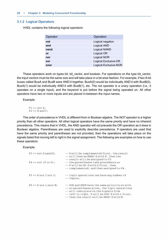
3.2.1 Logical Operator Example: SOP Circuit
Example 3.1 shows how to design a VHDLmodel of a standard sum of products’ combinational logic
circuit using concurrent signal assignments with logical operators.
Example 3.1SOP logic circuit: VHDL modeling using logical operators
3.2 Concurrent Signal Assignments with Logical Operators • 25
3.2.2 Logical Operator Example: One-Hot Decoder
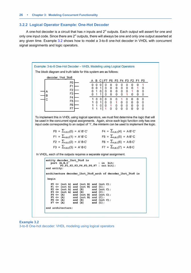
A one-hot decoder is a circuit that has n inputs and 2n outputs. Each output will assert for one and
only one input code. Since there are 2n outputs, there will always be one and only one output asserted at
any given time. Example 3.2 shows how to model a 3-to-8 one-hot decoder in VHDL with concurrent
signal assignments and logic operators.
Example 3.23-to-8 One-hot decoder: VHDL modeling using logical operators
26 • Chapter 3: Modeling Concurrent Functionality
3.2.3 Logical Operator Example: 7-Segment Display Decoder
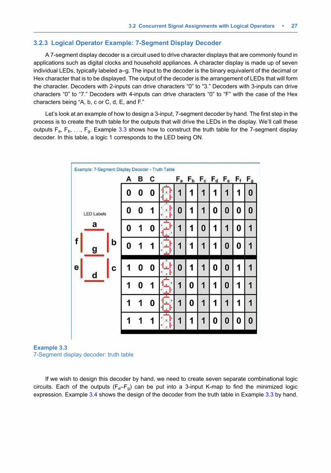
A 7-segment display decoder is a circuit used to drive character displays that are commonly found in
applications such as digital clocks and household appliances. A character display is made up of seven
individual LEDs, typically labeled a–g. The input to the decoder is the binary equivalent of the decimal or
Hex character that is to be displayed. The output of the decoder is the arrangement of LEDs that will form
the character. Decoders with 2-inputs can drive characters “0” to “3.” Decoders with 3-inputs can drive
characters “0” to “7.” Decoders with 4-inputs can drive characters “0” to “F” with the case of the Hex
characters being “A, b, c or C, d, E, and F.”
Let’s look at an example of how to design a 3-input, 7-segment decoder by hand. The first step in the
process is to create the truth table for the outputs that will drive the LEDs in the display. We’ll call these
outputs Fa, Fb, . . ., Fg. Example 3.3 shows how to construct the truth table for the 7-segment display
decoder. In this table, a logic 1 corresponds to the LED being ON.
If we wish to design this decoder by hand, we need to create seven separate combinational logic
circuits. Each of the outputs (Fa–Fg) can be put into a 3-input K-map to find the minimized logic
expression. Example 3.4 shows the design of the decoder from the truth table in Example 3.3 by hand.
Example 3.37-Segment display decoder: truth table
3.2 Concurrent Signal Assignments with Logical Operators • 27
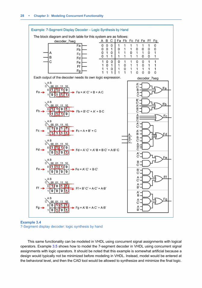
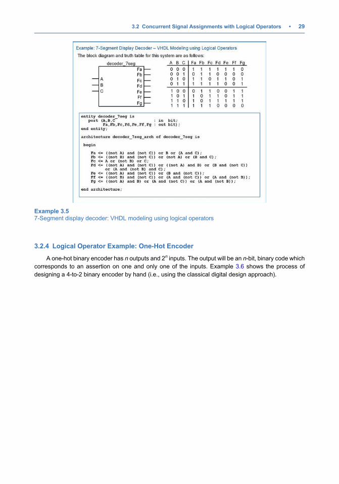
This same functionality can be modeled in VHDL using concurrent signal assignments with logical
operators. Example 3.5 shows how to model the 7-segment decoder in VHDL using concurrent signal
assignments with logic operators. It should be noted that this example is somewhat artificial because a
design would typically not be minimized before modeling in VHDL. Instead, model would be entered at
the behavioral level, and then the CAD tool would be allowed to synthesize and minimize the final logic.
Example 3.47-Segment display decoder: logic synthesis by hand
28 • Chapter 3: Modeling Concurrent Functionality
3.2.4 Logical Operator Example: One-Hot Encoder
A one-hot binary encoder has n outputs and 2n inputs. The output will be an n-bit, binary code which
corresponds to an assertion on one and only one of the inputs. Example 3.6 shows the process of
designing a 4-to-2 binary encoder by hand (i.e., using the classical digital design approach).
Example 3.57-Segment display decoder: VHDL modeling using logical operators
3.2 Concurrent Signal Assignments with Logical Operators • 29
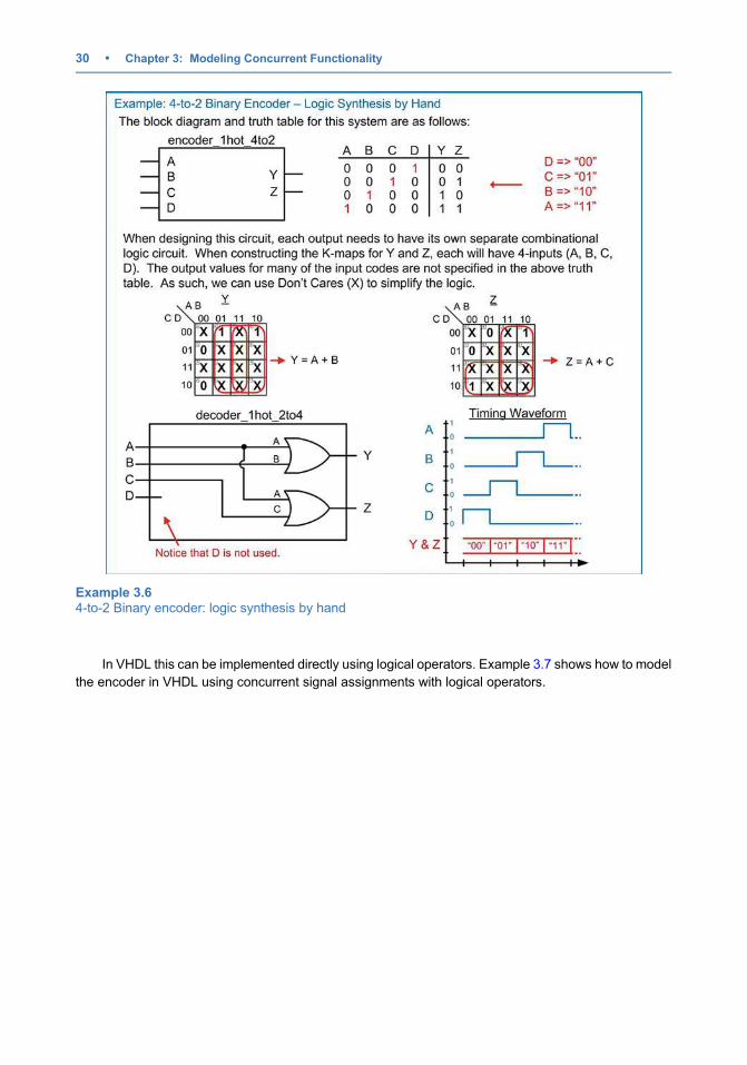
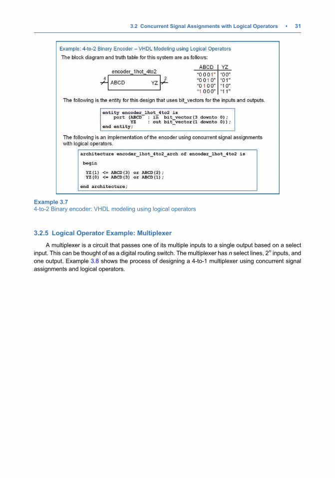
In VHDL this can be implemented directly using logical operators. Example 3.7 shows how to model
the encoder in VHDL using concurrent signal assignments with logical operators.
Example 3.64-to-2 Binary encoder: logic synthesis by hand
30 • Chapter 3: Modeling Concurrent Functionality
3.2.5 Logical Operator Example: Multiplexer
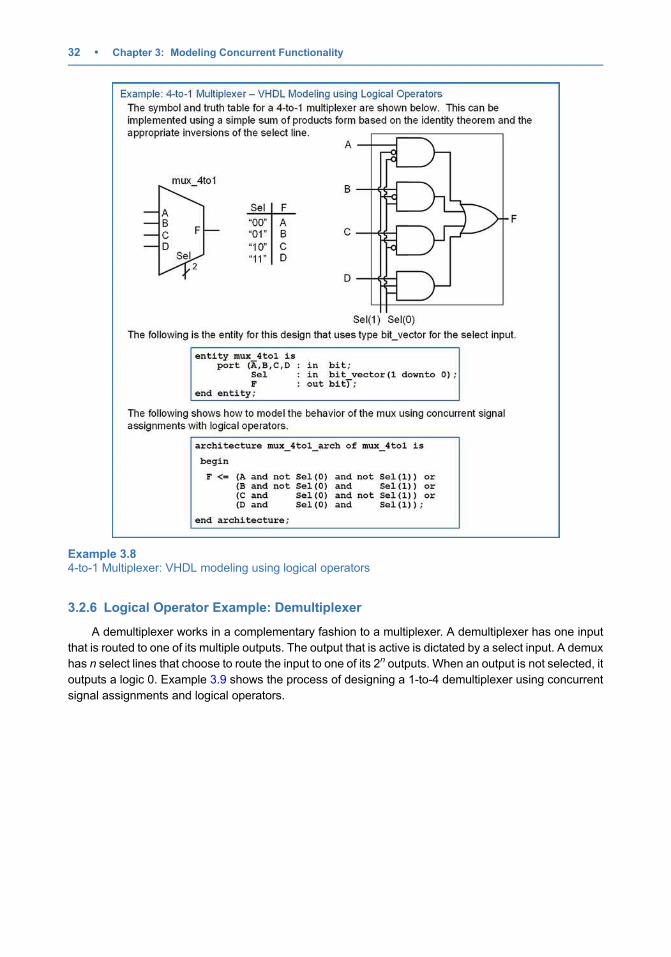
A multiplexer is a circuit that passes one of its multiple inputs to a single output based on a select
input. This can be thought of as a digital routing switch. The multiplexer has n select lines, 2n inputs, and
one output. Example 3.8 shows the process of designing a 4-to-1 multiplexer using concurrent signal
assignments and logical operators.
Example 3.74-to-2 Binary encoder: VHDL modeling using logical operators
3.2 Concurrent Signal Assignments with Logical Operators • 31
3.2.6 Logical Operator Example: Demultiplexer
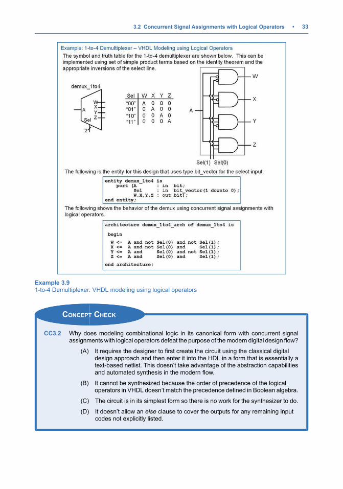
A demultiplexer works in a complementary fashion to a multiplexer. A demultiplexer has one input
that is routed to one of its multiple outputs. The output that is active is dictated by a select input. A demux
has n select lines that choose to route the input to one of its 2n outputs. When an output is not selected, it
outputs a logic 0. Example 3.9 shows the process of designing a 1-to-4 demultiplexer using concurrent
signal assignments and logical operators.
Example 3.84-to-1 Multiplexer: VHDL modeling using logical operators
32 • Chapter 3: Modeling Concurrent Functionality
CONCEPT CHECK
CC3.2 Why does modeling combinational logic in its canonical form with concurrent signalassignments with logical operators defeat the purpose of themodern digital design flow?
(A) It requires the designer to first create the circuit using the classical digitaldesign approach and then enter it into the HDL in a form that is essentially atext-based netlist. This doesn’t take advantage of the abstraction capabilitiesand automated synthesis in the modern flow.
(B) It cannot be synthesized because the order of precedence of the logicaloperators in VHDL doesn’t match the precedence defined in Boolean algebra.
(C) The circuit is in its simplest form so there is no work for the synthesizer to do.
(D) It doesn’t allow an else clause to cover the outputs for any remaining inputcodes not explicitly listed.
Example 3.91-to-4 Demultiplexer: VHDL modeling using logical operators
3.2 Concurrent Signal Assignments with Logical Operators • 33
3.3 Conditional Signal Assignments
Logical operators are good for describing the behavior of small circuits; however, in the prior
example, we still needed to create the canonical or minimal sum of products logic expression by hand
before describing the functionality in VHDL. The true power of an HDL is when the behavior of the system
can be described fully without requiring any hand design. A conditional signal assignment allows us to
describe a concurrent signal assignment using Boolean conditions that effect the values of the result. In a
conditional signal assignment, the keyword when is used to describe the signal assignment for a
particular Boolean condition. The keyword else is used to describe the signal assignments for any
other conditions. Multiple Boolean conditions can be used to fully describe the output of the circuit under
all input conditions. Logical operators can also be used in the Boolean conditions to create more
sophisticated conditions. The Boolean conditions can be encompassed within parentheses for readabil-
ity. The syntax for a conditional signal assignment is shown below.
signal_name <¼ expression_1 when condition_1 else
expression_2 when condition_2 else
:expression_n;
Example:
F1 <¼ ‘0’ when A¼‘0’ else ‘1’;F2 <¼ ‘1’ when (A¼’0’ and B¼’1’) else ‘0’;F3 <¼ A when (C ¼ D) else B;
An important consideration of conditional signal assignments is that they are still executed concur-
rently. Each assignment represents a separate, combinational logic circuit. In the above example, F1,
F2, and F3 will be implemented as three separate, parallel circuits.
3.3.1 Conditional Signal Assignment Example: SOP Circuit
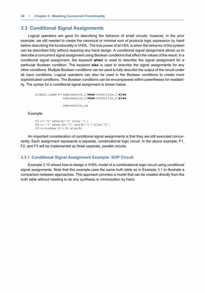
Example 3.10 shows how to design a VHDL model of a combinational logic circuit using conditional
signal assignments. Note that this example uses the same truth table as in Example 3.1 to illustrate a
comparison between approaches. This approach provides a model that can be created directly from the
truth table without needing to do any synthesis or minimization by hand.
34 • Chapter 3: Modeling Concurrent Functionality
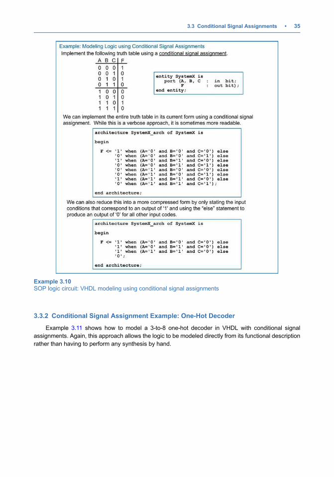
3.3.2 Conditional Signal Assignment Example: One-Hot Decoder
Example 3.11 shows how to model a 3-to-8 one-hot decoder in VHDL with conditional signal
assignments. Again, this approach allows the logic to be modeled directly from its functional description
rather than having to perform any synthesis by hand.
Example 3.10SOP logic circuit: VHDL modeling using conditional signal assignments
3.3 Conditional Signal Assignments • 35
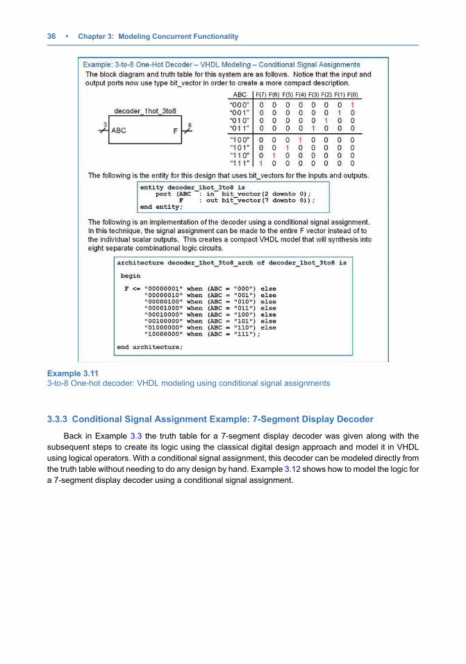
3.3.3 Conditional Signal Assignment Example: 7-Segment Display Decoder
Back in Example 3.3 the truth table for a 7-segment display decoder was given along with the
subsequent steps to create its logic using the classical digital design approach and model it in VHDL
using logical operators. With a conditional signal assignment, this decoder can be modeled directly from
the truth table without needing to do any design by hand. Example 3.12 shows how to model the logic for
a 7-segment display decoder using a conditional signal assignment.
Example 3.113-to-8 One-hot decoder: VHDL modeling using conditional signal assignments
36 • Chapter 3: Modeling Concurrent Functionality
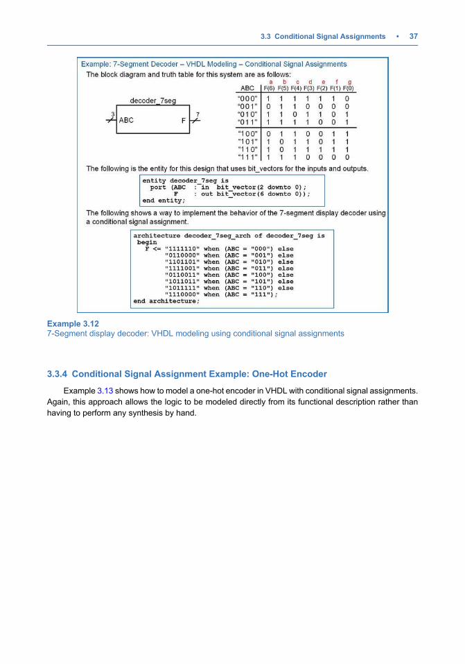
3.3.4 Conditional Signal Assignment Example: One-Hot Encoder
Example 3.13 shows how to model a one-hot encoder in VHDL with conditional signal assignments.
Again, this approach allows the logic to be modeled directly from its functional description rather than
having to perform any synthesis by hand.
Example 3.127-Segment display decoder: VHDL modeling using conditional signal assignments
3.3 Conditional Signal Assignments • 37
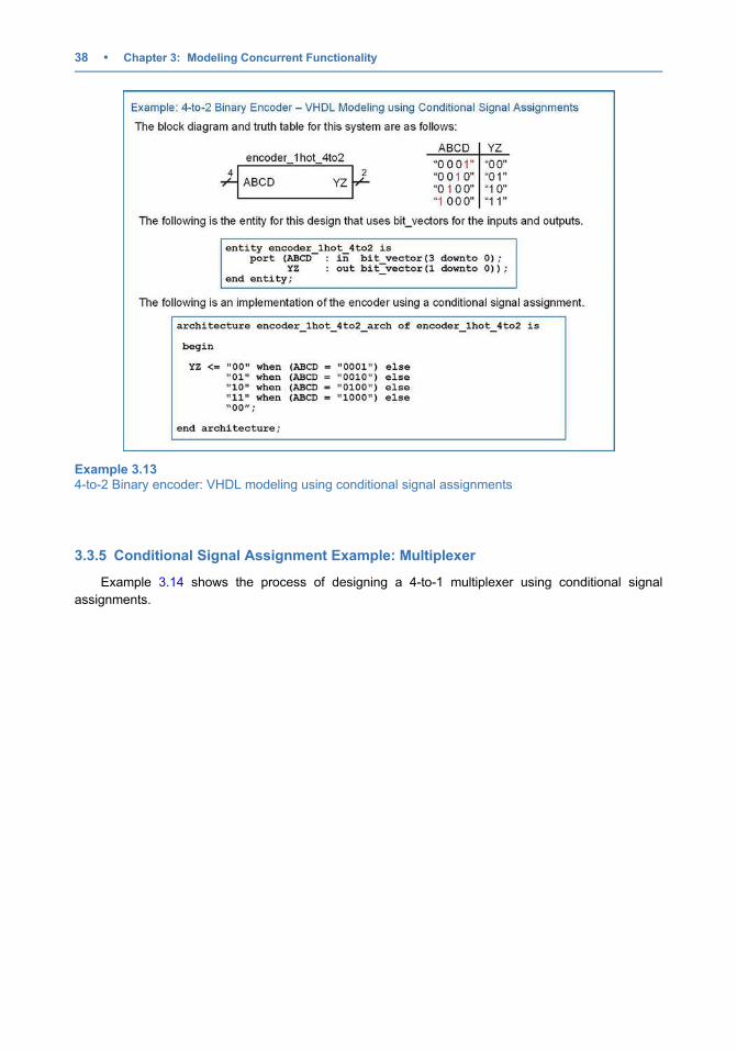
3.3.5 Conditional Signal Assignment Example: Multiplexer
Example 3.14 shows the process of designing a 4-to-1 multiplexer using conditional signal
assignments.
Example 3.134-to-2 Binary encoder: VHDL modeling using conditional signal assignments
38 • Chapter 3: Modeling Concurrent Functionality
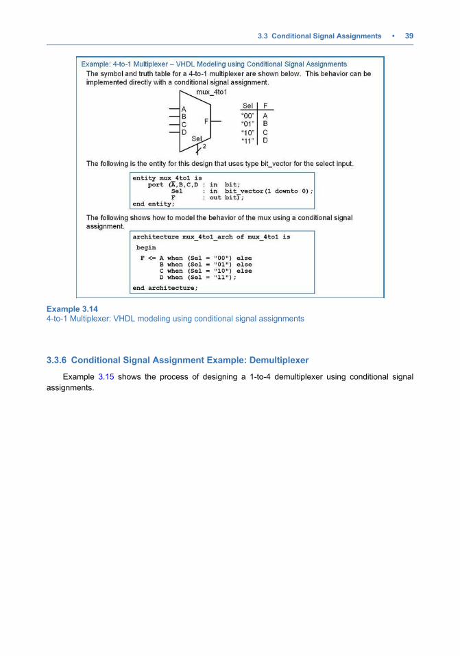
3.3.6 Conditional Signal Assignment Example: Demultiplexer
Example 3.15 shows the process of designing a 1-to-4 demultiplexer using conditional signal
assignments.
Example 3.144-to-1 Multiplexer: VHDL modeling using conditional signal assignments
3.3 Conditional Signal Assignments • 39
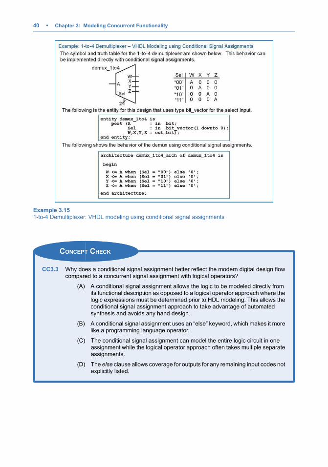
CONCEPT CHECK
CC3.3 Why does a conditional signal assignment better reflect the modern digital design flowcompared to a concurrent signal assignment with logical operators?
(A) A conditional signal assignment allows the logic to be modeled directly fromits functional description as opposed to a logical operator approach where thelogic expressions must be determined prior to HDL modeling. This allows theconditional signal assignment approach to take advantage of automatedsynthesis and avoids any hand design.
(B) A conditional signal assignment uses an “else” keyword, which makes it morelike a programming language operator.
(C) The conditional signal assignment can model the entire logic circuit in oneassignment while the logical operator approach often takes multiple separateassignments.
(D) The else clause allows coverage for outputs for any remaining input codes notexplicitly listed.
Example 3.151-to-4 Demultiplexer: VHDL modeling using conditional signal assignments
40 • Chapter 3: Modeling Concurrent Functionality
3.4 Selected Signal Assignments
A selected signal assignment provides another technique to implement concurrent signal
assignments. In this approach, the signal assignment is based on a specific value on the input signal.
The keyword with is used to begin the selected signal assignment. It is then followed by the name of the
input that will be used to dictate the value of the output. Only a single variable name can be listed as the
input. This means that if the assignment is going to be based on multiple variables, they must first be
concatenated into a single vector name before starting the selected signal assignment. After the input is
listed, the keyword select signifies the beginning of the signal assignments. An assignment is made to a
signal based on a list of possible input values that follow the keyword when. Multiple values of the input
codes can be used and are separated by commas. The keyword others is used to cover any input values
that are not explicitly stated. The syntax for a selected signal assignment is as follows:
with input_name selectsignal_name <¼ expression_1 when condition_1,
expression_2 when condition_2,:
expression_n when others;
Example:
with A selectF1 <¼ ‘1’ when ‘0’, -- F1 will be assigned ‘1’ when A¼’0’
‘0’ when ‘1’; -- F1 will be assigned ‘0’ when A¼’1’
AB <¼ A&B; -- concatenate A and B so that they can be used as a vectorwith AB selectF2 <¼ ‘0’ when “00”, -- F2 will be assigned ‘0’ when AB¼”00”
‘1’ when “01”,‘1’ when “10”,‘0’ when “11”;
with AB selectF3 <¼ ‘1’ when “01”,
‘1’ when “10”,‘0’ when others;
One feature of selected signal assignments that makes its form even more compact than other
techniques is that multiple input codes that correspond to the same output assignment can be listed on
the same line pipe (|)-delimited. The example for F3 can be equivalently described as:
with AB selectF3 <¼ ‘1’ when “01” | “10”,
‘0’ when others;
3.4.1 Selected Signal Assignment Example: SOP Circuit
Example 3.16 shows how to design a VHDL model of a combinational logic circuit using selected
signal assignments. Note that this example uses the same truth table as in Example 3.1 to illustrate a
comparison between approaches. This approach provides a model that can be created directly from the
truth table without needing to do any synthesis or minimization by hand.
3.4 Selected Signal Assignments • 41
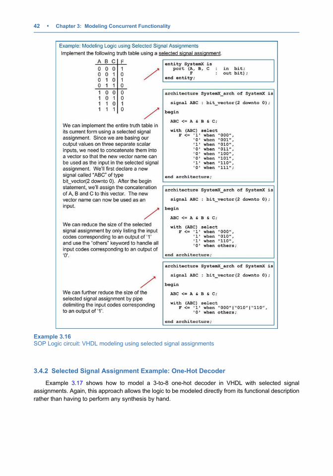
3.4.2 Selected Signal Assignment Example: One-Hot Decoder
Example 3.17 shows how to model a 3-to-8 one-hot decoder in VHDL with selected signal
assignments. Again, this approach allows the logic to be modeled directly from its functional description
rather than having to perform any synthesis by hand.
Example 3.16SOP Logic circuit: VHDL modeling using selected signal assignments
42 • Chapter 3: Modeling Concurrent Functionality
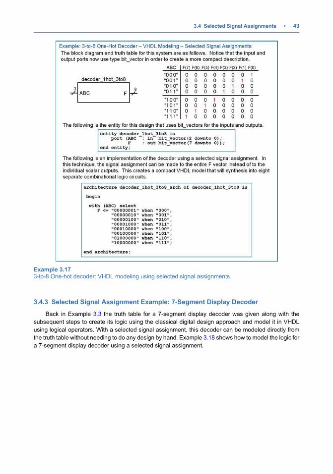
3.4.3 Selected Signal Assignment Example: 7-Segment Display Decoder
Back in Example 3.3 the truth table for a 7-segment display decoder was given along with the
subsequent steps to create its logic using the classical digital design approach and model it in VHDL
using logical operators. With a selected signal assignment, this decoder can be modeled directly from
the truth table without needing to do any design by hand. Example 3.18 shows how to model the logic for
a 7-segment display decoder using a selected signal assignment.
Example 3.173-to-8 One-hot decoder: VHDL modeling using selected signal assignments
3.4 Selected Signal Assignments • 43
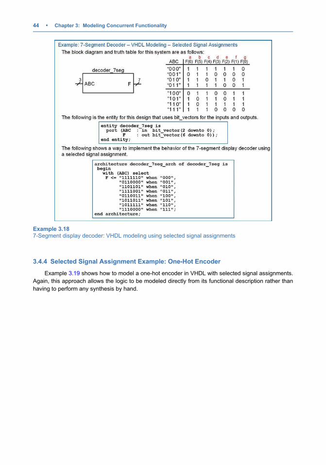
3.4.4 Selected Signal Assignment Example: One-Hot Encoder
Example 3.19 shows how to model a one-hot encoder in VHDL with selected signal assignments.
Again, this approach allows the logic to be modeled directly from its functional description rather than
having to perform any synthesis by hand.
Example 3.187-Segment display decoder: VHDL modeling using selected signal assignments
44 • Chapter 3: Modeling Concurrent Functionality
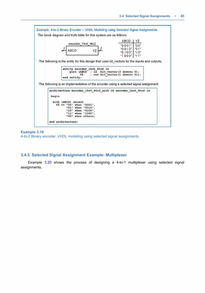
3.4.5 Selected Signal Assignment Example: Multiplexer
Example 3.20 shows the process of designing a 4-to-1 multiplexer using selected signal
assignments.
Example 3.194-to-2 Binary encoder: VHDL modeling using selected signal assignments
3.4 Selected Signal Assignments • 45
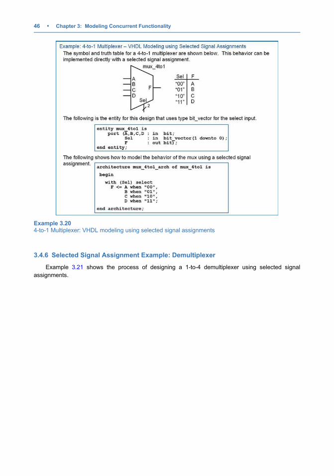
3.4.6 Selected Signal Assignment Example: Demultiplexer
Example 3.21 shows the process of designing a 1-to-4 demultiplexer using selected signal
assignments.
Example 3.204-to-1 Multiplexer: VHDL modeling using selected signal assignments
46 • Chapter 3: Modeling Concurrent Functionality
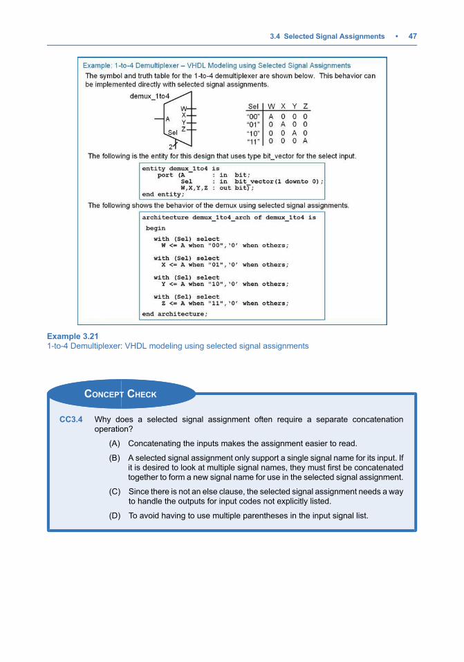
CONCEPT CHECK
CC3.4 Why does a selected signal assignment often require a separate concatenationoperation?
(A) Concatenating the inputs makes the assignment easier to read.
(B) A selected signal assignment only support a single signal name for its input. Ifit is desired to look at multiple signal names, they must first be concatenatedtogether to form a new signal name for use in the selected signal assignment.
(C) Since there is not an else clause, the selected signal assignment needs a wayto handle the outputs for input codes not explicitly listed.
(D) To avoid having to use multiple parentheses in the input signal list.
Example 3.211-to-4 Demultiplexer: VHDL modeling using selected signal assignments
3.4 Selected Signal Assignments • 47
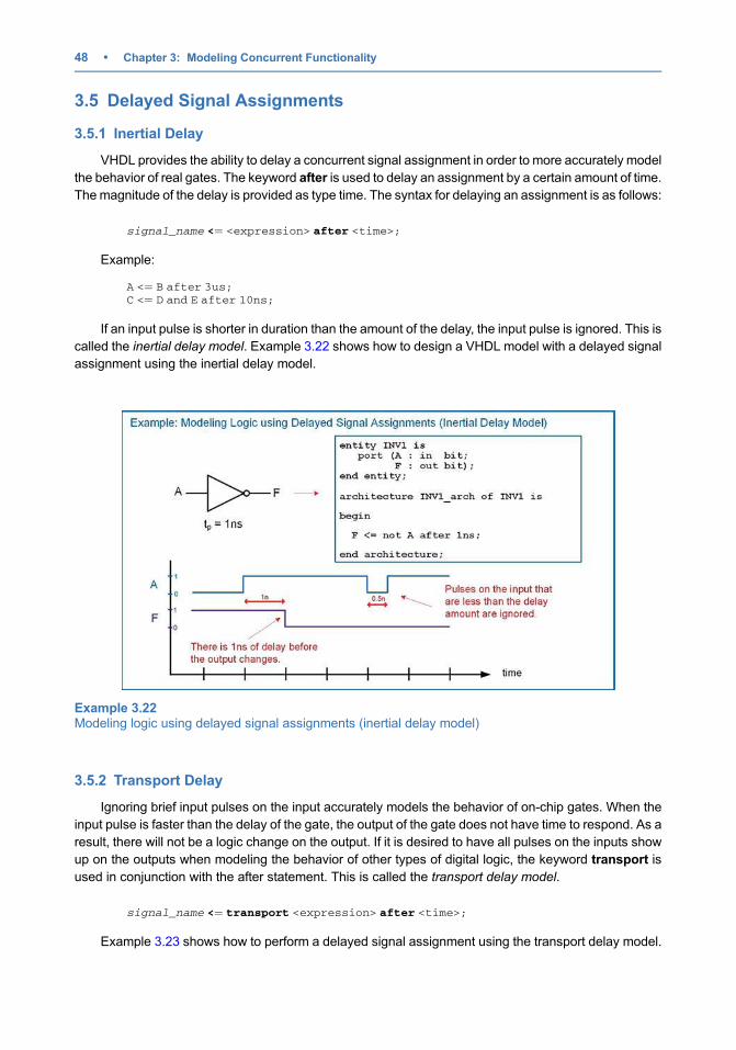
3.5 Delayed Signal Assignments
3.5.1 Inertial Delay
VHDL provides the ability to delay a concurrent signal assignment in order to more accurately model
the behavior of real gates. The keyword after is used to delay an assignment by a certain amount of time.
The magnitude of the delay is provided as type time. The syntax for delaying an assignment is as follows:
signal_name <¼ <expression> after <time>;
Example:
A <¼ B after 3us;C <¼ D and E after 10ns;
If an input pulse is shorter in duration than the amount of the delay, the input pulse is ignored. This is
called the inertial delay model. Example 3.22 shows how to design a VHDL model with a delayed signal
assignment using the inertial delay model.
3.5.2 Transport Delay
Ignoring brief input pulses on the input accurately models the behavior of on-chip gates. When the
input pulse is faster than the delay of the gate, the output of the gate does not have time to respond. As a
result, there will not be a logic change on the output. If it is desired to have all pulses on the inputs show
up on the outputs when modeling the behavior of other types of digital logic, the keyword transport is
used in conjunction with the after statement. This is called the transport delay model.
signal_name <¼ transport <expression> after <time>;
Example 3.23 shows how to perform a delayed signal assignment using the transport delay model.
Example 3.22Modeling logic using delayed signal assignments (inertial delay model)
48 • Chapter 3: Modeling Concurrent Functionality
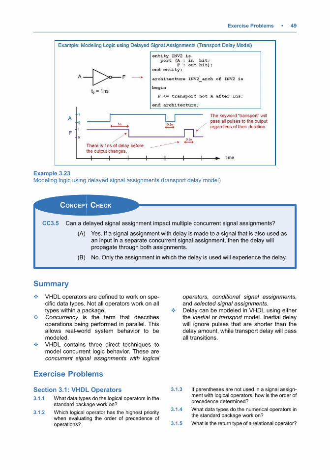
CONCEPT CHECK
CC3.5 Can a delayed signal assignment impact multiple concurrent signal assignments?
(A) Yes. If a signal assignment with delay is made to a signal that is also used asan input in a separate concurrent signal assignment, then the delay willpropagate through both assignments.
(B) No. Only the assignment in which the delay is used will experience the delay.
Summary
v VHDL operators are defined to work on spe-cific data types. Not all operators work on alltypes within a package.
v Concurrency is the term that describesoperations being performed in parallel. Thisallows real-world system behavior to bemodeled.
v VHDL contains three direct techniques tomodel concurrent logic behavior. These areconcurrent signal assignments with logical
operators, conditional signal assignments,and selected signal assignments.
v Delay can be modeled in VHDL using eitherthe inertial or transport model. Inertial delaywill ignore pulses that are shorter than thedelay amount, while transport delay will passall transitions.
Exercise Problems
Section 3.1: VHDL Operators
3.1.1 What data types do the logical operators in thestandard package work on?
3.1.2 Which logical operator has the highest prioritywhen evaluating the order of precedence ofoperations?
3.1.3 If parentheses are not used in a signal assign-ment with logical operators, how is the order ofprecedence determined?
3.1.4 What data types do the numerical operators inthe standard package work on?
3.1.5 What is the return type of a relational operator?
Example 3.23Modeling logic using delayed signal assignments (transport delay model)
Exercise Problems • 49
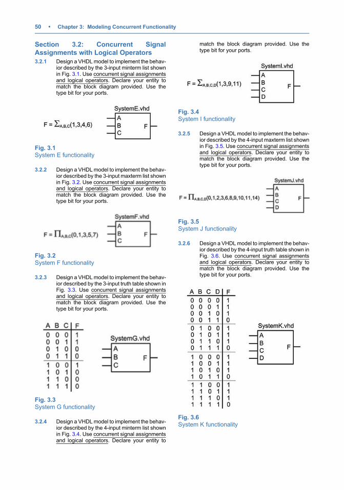
Section 3.2: Concurrent Signal
Assignments with Logical Operators
3.2.1 Design a VHDLmodel to implement the behav-ior described by the 3-input minterm list shownin Fig. 3.1. Use concurrent signal assignmentsand logical operators. Declare your entity tomatch the block diagram provided. Use thetype bit for your ports.
Fig. 3.1System E functionality
3.2.2 Design a VHDLmodel to implement the behav-ior described by the 3-input maxterm list shownin Fig. 3.2. Use concurrent signal assignmentsand logical operators. Declare your entity tomatch the block diagram provided. Use thetype bit for your ports.
Fig. 3.2System F functionality
3.2.3 Design a VHDLmodel to implement the behav-ior described by the 3-input truth table shown inFig. 3.3. Use concurrent signal assignmentsand logical operators. Declare your entity tomatch the block diagram provided. Use thetype bit for your ports.
Fig. 3.3System G functionality
3.2.4 Design a VHDLmodel to implement the behav-ior described by the 4-input minterm list shownin Fig. 3.4. Use concurrent signal assignmentsand logical operators. Declare your entity to
match the block diagram provided. Use thetype bit for your ports.
Fig. 3.4System I functionality
3.2.5 Design a VHDLmodel to implement the behav-ior described by the 4-input maxterm list shownin Fig. 3.5. Use concurrent signal assignmentsand logical operators. Declare your entity tomatch the block diagram provided. Use thetype bit for your ports.
Fig. 3.5System J functionality
3.2.6 Design a VHDLmodel to implement the behav-ior described by the 4-input truth table shown inFig. 3.6. Use concurrent signal assignmentsand logical operators. Declare your entity tomatch the block diagram provided. Use thetype bit for your ports.
Fig. 3.6System K functionality
50 • Chapter 3: Modeling Concurrent Functionality
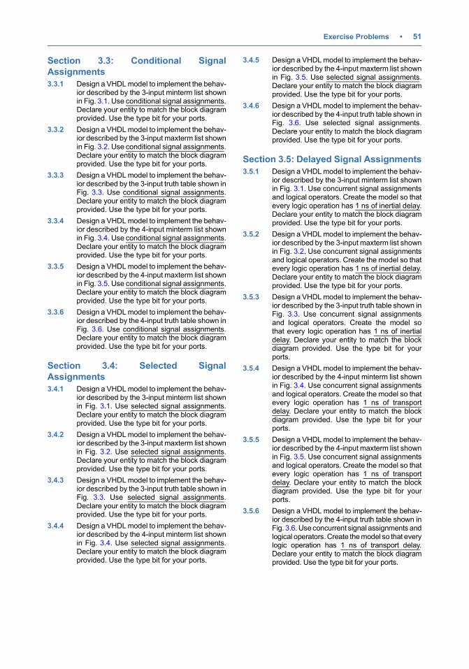
Section 3.3: Conditional Signal
Assignments
3.3.1 Design a VHDLmodel to implement the behav-ior described by the 3-input minterm list shownin Fig. 3.1. Use conditional signal assignments.Declare your entity to match the block diagramprovided. Use the type bit for your ports.
3.3.2 Design a VHDLmodel to implement the behav-ior described by the 3-input maxterm list shownin Fig. 3.2. Use conditional signal assignments.Declare your entity to match the block diagramprovided. Use the type bit for your ports.
3.3.3 Design a VHDLmodel to implement the behav-ior described by the 3-input truth table shown inFig. 3.3. Use conditional signal assignments.Declare your entity to match the block diagramprovided. Use the type bit for your ports.
3.3.4 Design a VHDLmodel to implement the behav-ior described by the 4-input minterm list shownin Fig. 3.4. Use conditional signal assignments.Declare your entity to match the block diagramprovided. Use the type bit for your ports.
3.3.5 Design a VHDLmodel to implement the behav-ior described by the 4-input maxterm list shownin Fig. 3.5. Use conditional signal assignments.Declare your entity to match the block diagramprovided. Use the type bit for your ports.
3.3.6 Design a VHDLmodel to implement the behav-ior described by the 4-input truth table shown inFig. 3.6. Use conditional signal assignments.Declare your entity to match the block diagramprovided. Use the type bit for your ports.
Section 3.4: Selected Signal
Assignments
3.4.1 Design a VHDLmodel to implement the behav-ior described by the 3-input minterm list shownin Fig. 3.1. Use selected signal assignments.Declare your entity to match the block diagramprovided. Use the type bit for your ports.
3.4.2 Design a VHDLmodel to implement the behav-ior described by the 3-input maxterm list shownin Fig. 3.2. Use selected signal assignments.Declare your entity to match the block diagramprovided. Use the type bit for your ports.
3.4.3 Design a VHDLmodel to implement the behav-ior described by the 3-input truth table shown inFig. 3.3. Use selected signal assignments.Declare your entity to match the block diagramprovided. Use the type bit for your ports.
3.4.4 Design a VHDLmodel to implement the behav-ior described by the 4-input minterm list shownin Fig. 3.4. Use selected signal assignments.Declare your entity to match the block diagramprovided. Use the type bit for your ports.
3.4.5 Design a VHDLmodel to implement the behav-ior described by the 4-input maxterm list shownin Fig. 3.5. Use selected signal assignments.Declare your entity to match the block diagramprovided. Use the type bit for your ports.
3.4.6 Design a VHDLmodel to implement the behav-ior described by the 4-input truth table shown inFig. 3.6. Use selected signal assignments.Declare your entity to match the block diagramprovided. Use the type bit for your ports.
Section 3.5: Delayed Signal Assignments
3.5.1 Design a VHDLmodel to implement the behav-ior described by the 3-input minterm list shownin Fig. 3.1. Use concurrent signal assignmentsand logical operators. Create the model so thatevery logic operation has 1 ns of inertial delay.Declare your entity to match the block diagramprovided. Use the type bit for your ports.
3.5.2 Design a VHDLmodel to implement the behav-ior described by the 3-input maxterm list shownin Fig. 3.2. Use concurrent signal assignmentsand logical operators. Create the model so thatevery logic operation has 1 ns of inertial delay.Declare your entity to match the block diagramprovided. Use the type bit for your ports.
3.5.3 Design a VHDLmodel to implement the behav-ior described by the 3-input truth table shown inFig. 3.3. Use concurrent signal assignmentsand logical operators. Create the model sothat every logic operation has 1 ns of inertialdelay. Declare your entity to match the blockdiagram provided. Use the type bit for yourports.
3.5.4 Design a VHDLmodel to implement the behav-ior described by the 4-input minterm list shownin Fig. 3.4. Use concurrent signal assignmentsand logical operators. Create the model so thatevery logic operation has 1 ns of transportdelay. Declare your entity to match the blockdiagram provided. Use the type bit for yourports.
3.5.5 Design a VHDLmodel to implement the behav-ior described by the 4-input maxterm list shownin Fig. 3.5. Use concurrent signal assignmentsand logical operators. Create the model so thatevery logic operation has 1 ns of transportdelay. Declare your entity to match the blockdiagram provided. Use the type bit for yourports.
3.5.6 Design a VHDL model to implement the behav-ior described by the 4-input truth table shown inFig. 3.6. Use concurrent signal assignments andlogical operators.Create themodel so that everylogic operation has 1 ns of transport delay.Declare your entity to match the block diagramprovided. Use the type bit for your ports.
Exercise Problems • 51
Chapter 4: Structural Design
and HierarchyThis chapter describes how to accomplish hierarchy within VHDL using lower-level sub-systems.
Structural design in VHDL refers to including lower-level sub-systems within a higher-level system in
order to produce the desired functionality. A purely structural VHDL design would not contain any
behavioral modeling in the architecture such as signal assignments but instead just contain the instanti-
ation and interconnections of other sub-systems.
Learning Outcomes—After completing this chapter, you will be able to:
4.1 Instantiate and map the ports of a lower-level component in VHDL.4.2 Design a VHDL model for a system that uses hierarchy.
4.1 Components
4.1.1 Component Instantiation
A sub-system is called a component in VHDL. For any component that is going to be used in an
architecture, it must be declared before the begin statement. Refer to Sect. 2.2.3.3 for the syntax of
declaring a component. A specific component only needs to be declared once. After the begin statement,
it can be used as many times as necessary. Each component is executed concurrently.
The term instantiation refers to the use or inclusion of the component in the VHDL system. When a
component is instantiated, it needs to be given a unique identifying name. This is called the instance
name. To instantiate a component, the instance name is given first, followed by a colon and then the
component name. The last part of instantiating a component is connecting signals to its ports. The way in
which signals are connected to the ports of the component is called the port map. The syntax for
instantiating a component is as follows:
instance_name : <component name>
port map (<port connections>);
4.1.2 Port Mapping
There are two techniques to connect signals to the ports of the component, explicit port mapping
and positional port mapping.
4.1.2.1 Explicit Port Mapping
In explicit port mapping, the name of each port of the component is given, followed by the connection
indicator ¼>, followed by the signal it is connected to. The port connections can be listed in any order
since the details of the connection (i.e., port name to signal name) are explicit. Each connection name is
separated by a comma. The syntax for explicit port mapping is as follows:
instance_name : <component name>
port map (port1 ¼> signal1, port2 ¼> signal2, ...);
# Springer Nature Switzerland AG 2019
B. J. LaMeres, Quick Start Guide to VHDL, https://doi.org/10.1007/978-3-030-04516-6_4
53
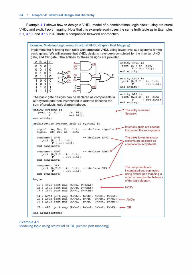
Example 4.1 shows how to design a VHDL model of a combinational logic circuit using structural
VHDL and explicit port mapping. Note that this example again uses the same truth table as in Examples
3.1, 3.10, and 3.16 to illustrate a comparison between approaches.
Example 4.1Modeling logic using structural VHDL (explicit port mapping)
54 • Chapter 4: Structural Design and Hierarchy
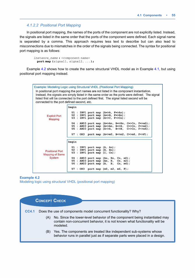
4.1.2.2 Positional Port Mapping
In positional port mapping, the names of the ports of the component are not explicitly listed. Instead,
the signals are listed in the same order that the ports of the component were defined. Each signal name
is separated by a comma. This approach requires less text to describe but can also lead to
misconnections due to mismatches in the order of the signals being connected. The syntax for positional
port mapping is as follows:
instance_name : <component name>
port map (signal1, signal2, ...);
Example 4.2 shows how to create the same structural VHDL model as in Example 4.1, but using
positional port mapping instead.
CONCEPT CHECK
CC4.1 Does the use of components model concurrent functionality? Why?
(A) No. Since the lower-level behavior of the component being instantiated maycontain non-concurrent behavior, it is not known what functionality will bemodeled.
(B) Yes. The components are treated like independent sub-systems whosebehavior runs in parallel just as if separate parts were placed in a design.
Example 4.2Modeling logic using structural VHDL (positional port mapping)
4.1 Components • 55
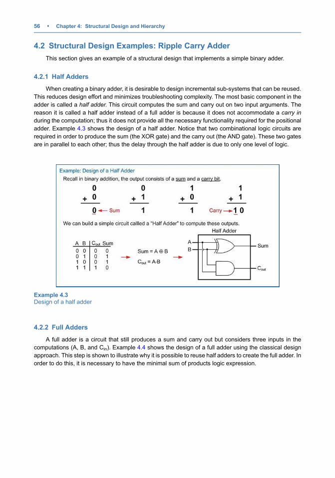
4.2 Structural Design Examples: Ripple Carry Adder
This section gives an example of a structural design that implements a simple binary adder.
4.2.1 Half Adders
When creating a binary adder, it is desirable to design incremental sub-systems that can be reused.
This reduces design effort and minimizes troubleshooting complexity. The most basic component in the
adder is called a half adder. This circuit computes the sum and carry out on two input arguments. The
reason it is called a half adder instead of a full adder is because it does not accommodate a carry in
during the computation; thus it does not provide all the necessary functionality required for the positional
adder. Example 4.3 shows the design of a half adder. Notice that two combinational logic circuits are
required in order to produce the sum (the XOR gate) and the carry out (the AND gate). These two gates
are in parallel to each other; thus the delay through the half adder is due to only one level of logic.
4.2.2 Full Adders
A full adder is a circuit that still produces a sum and carry out but considers three inputs in the
computations (A, B, and Cin). Example 4.4 shows the design of a full adder using the classical design
approach. This step is shown to illustrate why it is possible to reuse half adders to create the full adder. In
order to do this, it is necessary to have the minimal sum of products logic expression.
Example 4.3Design of a half adder
56 • Chapter 4: Structural Design and Hierarchy
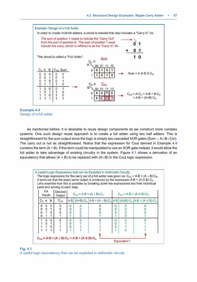
As mentioned before, it is desirable to reuse design components as we construct more complex
systems. One such design reuse approach is to create a full adder using two half adders. This is
straightforward for the sum output since the logic is simply two cascaded XOR gates (Sum¼ A�B�Cin).
The carry out is not as straightforward. Notice that the expression for Cout derived in Example 4.4
contains the term (A + B). If this term could be manipulated to use an XOR gate instead, it would allow the
full adder to take advantage of existing circuitry in the system. Figure 4.1 shows a derivation of an
equivalency that allows (A + B) to be replaced with (A�B) in the Cout logic expression.
Example 4.4Design of a full adder
Fig. 4.1A useful logic equivalency that can be exploited in arithmetic circuits
4.2 Structural Design Examples: Ripple Carry Adder • 57
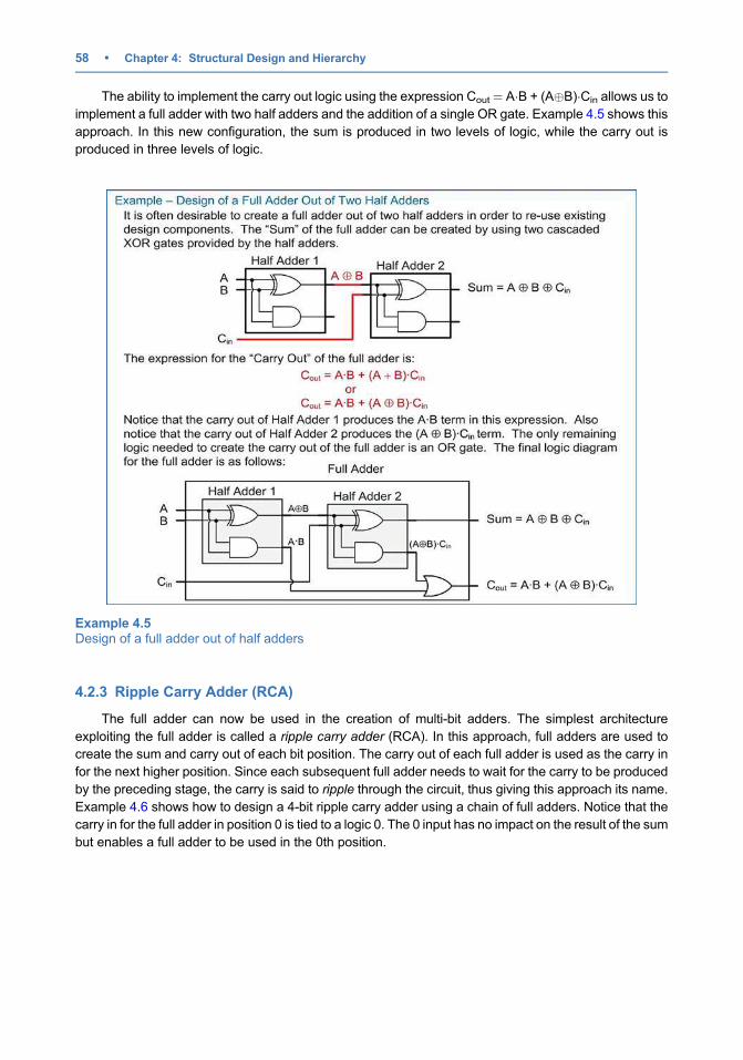
The ability to implement the carry out logic using the expression Cout ¼ A�B + (A�B)�Cin allows us to
implement a full adder with two half adders and the addition of a single OR gate. Example 4.5 shows this
approach. In this new configuration, the sum is produced in two levels of logic, while the carry out is
produced in three levels of logic.
4.2.3 Ripple Carry Adder (RCA)
The full adder can now be used in the creation of multi-bit adders. The simplest architecture
exploiting the full adder is called a ripple carry adder (RCA). In this approach, full adders are used to
create the sum and carry out of each bit position. The carry out of each full adder is used as the carry in
for the next higher position. Since each subsequent full adder needs to wait for the carry to be produced
by the preceding stage, the carry is said to ripple through the circuit, thus giving this approach its name.
Example 4.6 shows how to design a 4-bit ripple carry adder using a chain of full adders. Notice that the
carry in for the full adder in position 0 is tied to a logic 0. The 0 input has no impact on the result of the sum
but enables a full adder to be used in the 0th position.
Example 4.5Design of a full adder out of half adders
58 • Chapter 4: Structural Design and Hierarchy
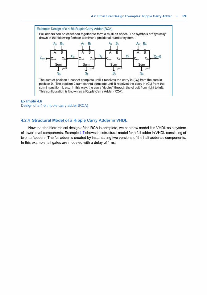
4.2.4 Structural Model of a Ripple Carry Adder in VHDL
Now that the hierarchical design of the RCA is complete, we can now model it in VHDL as a system
of lower-level components. Example 4.7 shows the structural model for a full adder in VHDL consisting of
two half adders. The full adder is created by instantiating two versions of the half adder as components.
In this example, all gates are modeled with a delay of 1 ns.
Example 4.6Design of a 4-bit ripple carry adder (RCA)
4.2 Structural Design Examples: Ripple Carry Adder • 59
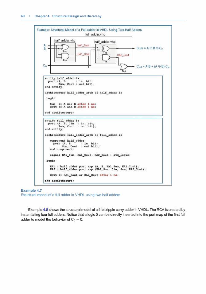
Example 4.8 shows the structural model of a 4-bit ripple carry adder in VHDL. The RCA is created by
instantiating four full adders. Notice that a logic 0 can be directly inserted into the port map of the first full
adder to model the behavior of C0 ¼ 0.
Example 4.7Structural model of a full adder in VHDL using two half adders
60 • Chapter 4: Structural Design and Hierarchy
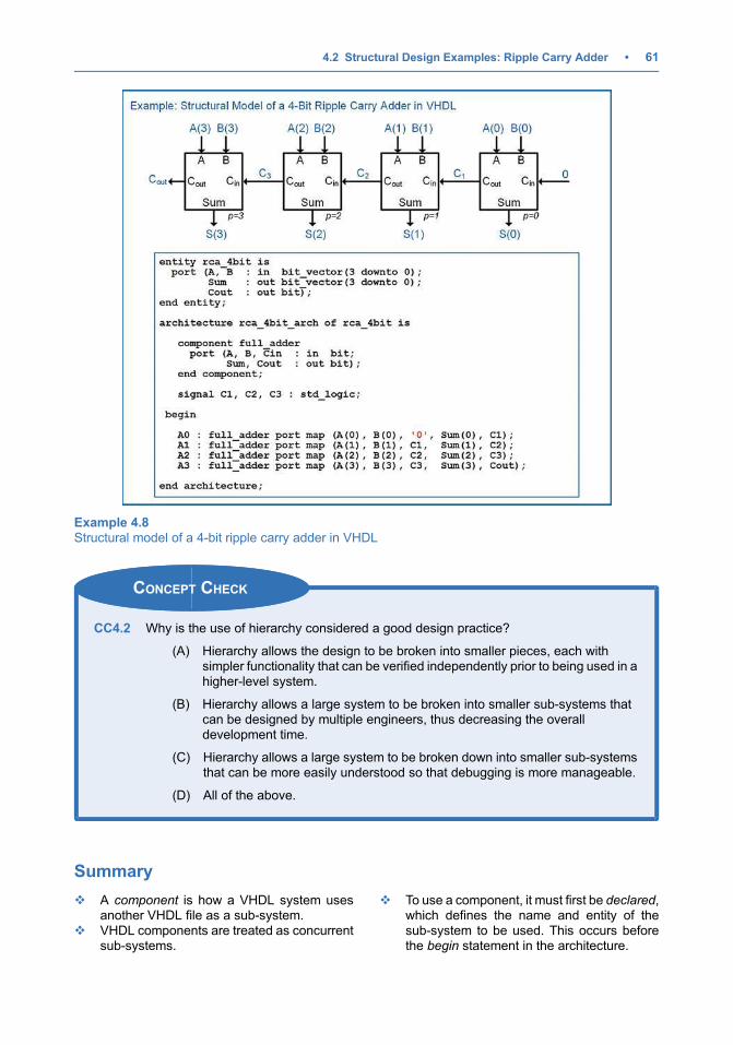
CONCEPT CHECK
CC4.2 Why is the use of hierarchy considered a good design practice?
(A) Hierarchy allows the design to be broken into smaller pieces, each withsimpler functionality that can be verified independently prior to being used in ahigher-level system.
(B) Hierarchy allows a large system to be broken into smaller sub-systems thatcan be designed by multiple engineers, thus decreasing the overalldevelopment time.
(C) Hierarchy allows a large system to be broken down into smaller sub-systemsthat can be more easily understood so that debugging is more manageable.
(D) All of the above.
Summary
v A component is how a VHDL system usesanother VHDL file as a sub-system.
v VHDL components are treated as concurrentsub-systems.
v To use a component, it must first be declared,which defines the name and entity of thesub-system to be used. This occurs beforethe begin statement in the architecture.
Example 4.8Structural model of a 4-bit ripple carry adder in VHDL
4.2 Structural Design Examples: Ripple Carry Adder • 61
v A component can be instantiated one ormore times, which includes one or more cop-ies of the sub-system in the higher-level sys-tem. This occurs after the begin statement inthe architecture.
v The ports of the component can beconnected using either explicit or positionalport mapping.
v Explicit port mapping involves listing both thenames of the lower-level component’s portsalong with the higher-level signals that formthe connection. The connections in explicitport mapping can be listed in any order.Explicit port mapping is less prone to mis-taken connections.
v Positional port mapping involves listing onlythe names of the higher-level signals duringinstantiation. The order in which the signalsare listed will be connected to the ports of thelower-level sub-system in the order that theports were declared. Positional port mappingprovides a more compact approach to portmapping. Positional port mapping is moreprone to mistaken connections due to poten-tially listing the signals in the wrong orderduring mapping.
Exercise Problems
Section 4.1: Components
4.1.1 Howmany times does a component need to bedeclared within an architecture?
4.1.2 How many times can a component beinstantiated?
4.1.3 Does declaring a component occur before orafter the begin statement in the architecture?
4.1.4 Does instantiating a component occur beforeor after the begin statement in thearchitecture?
4.1.5 Which port mapping technique is more com-pact, explicit or positional?
4.1.6 Which port mapping technique is less prone toconnection errors because the names of thelower-level ports are listed within the mapping?
Section 4.2: Structural Design Examples
4.2.1 Design a VHDLmodel to implement the behav-ior described by the 3-input minterm list shownin Fig. 3.1. Use a structural design approachand basic gates. You will need to create what-ever basic gates are needed for your design(e.g., INV1, AND2, OR4, etc.) and then instan-tiate them in your upper-level architecture tocreate the desired functionality. The lower-level gates can be implemented with concur-rent signal assignments and logical operators(e.g., F <¼ not A). Declare your entity to matchthe block diagram provided. Use the type bit foryour ports.
4.2.2 Design a VHDLmodel to implement the behav-ior described by the 3-input maxterm list shownin Fig. 3.2. Use a structural design approachand basic gates. You will need to create what-ever basic gates are needed for your design(e.g., INV1, AND2, OR4, etc.) and then instan-tiate them in your upper-level architecture tocreate the desired functionality. The lower-level gates can be implemented with concur-rent signal assignments and logical operators
(e.g., F <¼ not A). Declare your entity to matchthe block diagram provided. Use the type bit foryour ports.
4.2.3 Design a VHDLmodel to implement the behav-ior described by the 3-input truth table shown inFig. 3.3. Use a structural design approach andbasic gates. You will need to create whateverbasic gates are needed for your design (e.g.,INV1, AND2, OR4, etc.) and then instantiatethem in your upper-level architecture to createthe desired functionality. The lower-level gatescan be implemented with concurrent signalassignments and logical operators (e.g.,F <¼ not A). Declare your entity to match theblock diagram provided. Use the type bit foryour ports.
4.2.4 Design a VHDLmodel to implement the behav-ior described by the 4-input minterm list shownin Fig. 3.4. Use a structural design approachand basic gates. You will need to create what-ever basic gates are needed for your design(e.g., INV1, AND2, OR4, etc.) and then instan-tiate them in your upper-level architecture tocreate the desired functionality. The lower-level gates can be implemented with concur-rent signal assignments and logical operators(e.g., F <¼ not A). Declare your entity to matchthe block diagram provided. Use the type bit foryour ports.
4.2.5 Design a VHDLmodel to implement the behav-ior described by the 4-input maxterm list shownin Fig. 3.5. Use a structural design approachand basic gates. You will need to create what-ever basic gates are needed for your design(e.g., INV1, AND2, OR4, etc.) and then instan-tiate them in your upper-level architecture tocreate the desired functionality. The lower-level gates can be implemented with concur-rent signal assignments and logical operators(e.g., F <¼ not A). Declare your entity to matchthe block diagram provided. Use the type bit foryour ports.
62 • Chapter 4: Structural Design and Hierarchy
4.2.6 Design a VHDLmodel to implement the behav-ior described by the 4-input truth table shown inFig. 3.6. Use a structural design approach andbasic gates. You will need to create whateverbasic gates are needed for your design (e.g.,INV1, AND2, OR4, etc.) and then instantiatethem in your upper-level architecture to create
the desired functionality. The lower-level gatescan be implemented with concurrent signalassignments and logical operators (e.g.,F <¼ not A). Declare your entity to match theblock diagram provided. Use the type bit foryour ports.
Exercise Problems • 63
Chapter 5: Modeling Sequential
FunctionalityIn Chap. 3 techniques were presented to describe the behavior of concurrent systems. The
modeling techniques presented were appropriate for combinational logic because these types of circuits
have outputs dependent only on the current values of their inputs. This means a model that continuously
performs signal assignments provides an accurate model of this circuit behavior. When we start looking
at sequential circuits (i.e., D-flip-flops, registers, finite state machine, and counters), these devices only
update their outputs based upon an event, most often the edge of a clock signal. The modeling
techniques presented in Chap. 3 are unable to accurately describe this type of behavior. In this chapter
we describe the VHDL constructs to model signal assignments that are triggered by an event to
accurately model sequential logic. We can then use these techniques to describe more complex
sequential logic circuits such as finite state machines and register transfer level systems.
Learning Outcomes—After completing this chapter, you will be able to:
5.1 Describe the behavior of a VHDL process and how it is used to model sequential logiccircuits.
5.2 Model combinational logic circuits using a process and conditional programmingconstructs.
5.3 Describe how and why signal attributes are used in VHDL models.
5.1 The Process
VHDL uses a process to model signal assignments that are based on an event. A process is a
technique to model behavior of a system; thus, a process is placed in the VHDL architecture after the
begin statement. The signal assignments within a process have unique characteristics that allow
them to accurately model sequential logic. First, the signal assignments do not take place until the
process ends or is suspended. Second, the signal assignments will be made only once each time the
process is triggered. Finally, the signal assignments will be executed in the order that they appear
within the process. This assignment behavior is called a sequential signal assignment. Sequential
signal assignments allow a process to model register transfer level behavior where a signal can be
used as both the operand of an assignment and the destination of a different assignment within the
same process. VHDL provides two techniques to trigger a process, the sensitivity list and the wait
statement.
5.1.1 Sensitivity Lists
A sensitivity list is a mechanism to control when a process is triggered (or started). A sensitivity list
contains a list of signals that the process is sensitive to. If there is a transition on any of the signals in the
list, the process will be triggered, and the signal assignments in the process will be made. The following
is the syntax for a process that uses a sensitivity list.
# Springer Nature Switzerland AG 2019
B. J. LaMeres, Quick Start Guide to VHDL, https://doi.org/10.1007/978-3-030-04516-6_5
65
process_name : process (<signal_name1>, <signal_name2>, ...)
-- variable declarations
begin
sequential_signal_assignment_1sequential_signal_assignment_2
:end process;
Let’s look at a simple model for a flip-flop.
Example:
FlipFlop : process (Clock)begin
Q <¼ D;end process;
In this example, a transition on the signal Clock (LOW to HIGH or HIGH to LOW) will trigger the
process. The signal assignment of D to Q will be executed once the process ends. When the signal Clock
is not transitioning, the process will not trigger, and no assignments will be made to Q, thus modeling the
behavior of Q holding its last value. This behavior is close to modeling the behavior of a real D-flip-flop,
but more constructs are needed to model behavior that is sensitive to only a particular type of transition
(i.e., rising or falling edge). These constructs will be covered later.
5.1.2 Wait Statements
Await statement is a mechanism to suspend (or stop) a process and allow signal assignments to be
executed without the need for the process to end. When using a wait statement, a sensitivity list is not
used. Without a sensitivity list, the process will immediately trigger. Within the process, the wait
statement is used to stop and start the process. There are three ways in which wait statements can be
used. The first is an indefinite wait. In the following example, the process does not contain a sensitivity
list, so it will trigger immediately. The keyword wait is used to suspend the process. Once this statement
is reached, the signal assignments to Y1 and Y2 will be executed, and the process will suspend
indefinitely.
Example:
Proc_Ex1 : processbegin
Y1 <¼ ’0’;Y2 <¼ ’1’;wait;
end process;
The second technique to use a wait statement to suspend a process is to use it in conjunction with
the keyword for and a time expression. In the following example, the process will trigger immediately
since it does not contain a sensitivity list. Once the process reaches the wait statement, it will suspend
and execute the first signal assignment to CLK (CLK <¼ ‘0’). After 5 ns, the process will start again. Once
it reaches the second wait statement, it will suspend and execute the second signal assignment to CLK
(CLK <¼ ‘1’). After another 5 ns, the process will start again and immediately end due to the end process
statement. After the process ends, it will immediately trigger again due to the lack of a sensitivity list and
repeat the behavior just described. This behavior will continue indefinitely. This example creates a
square wave called CLK with a period of 10 ns.
66 • Chapter 5: Modeling Sequential Functionality
Example:
Proc_Ex2 : processbegin
CLK <¼ ’0’; wait for 5 ns;CLK <¼ ’1’; wait for 5 ns;
end process;
The third technique to use a wait statement to suspend a process is to use it in conjunction with the
keyword until and a Boolean condition. In the following example, the process will again trigger immedi-
ately because there is not a sensitivity list present. The process will then immediately suspend and only
resume once a Boolean condition becomes true (i.e., Counter > 15). Once this condition is true, the
process will start again. Once it reaches the second wait statement, it will execute the first signal
assignment to RollOver (RollOver <¼ ‘1’). After 1 ns, the process will resume. Once the process ends,
it will execute the second signal assignment to RollOver (RollOver <¼ ‘0’).
Example:
Proc_Ex3 : processbegin
wait until (Counter > 15); -- first wait statementRollOver <¼ ’1’; wait for 1 ns; -- second wait statementRollOver <¼ ’0’;
end process;
Wait statements are typically not synthesizable and are most often used for creating stimulus
patterns in test benches.
5.1.3 Sequential Signal Assignments
One of the more confusing concepts of a process is how sequential signal assignments behave. The
rules of signal assignments within a process are as follows:
• Signals cannot be declared within a process.
• Signal assignments do not take place until the process ends or suspends.
• Signal assignments are executed in the sequence they appear in the process (once theprocess ends or process suspends).
Let’s look at an example of how signals behave in a process. Example 5.1 shows the behavior of
sequential signal assignments when executed within a process. Intuitively, we would assume that F will
be the complement of A; however, due to the way that sequential signal assignments are performed
within a process, this is not the case. In order to understand this behavior, let’s look at the situation where
A transitions from a 0 to a 1 with B ¼ 0 and F ¼ 0 initially. This transition triggers the process since A is
listed in the sensitivity list. When the process triggers, A¼ 1 since this is where the input resides after the
triggering transition. The first signal assignment (B <¼ A) will cause B ¼ 1, but this assignment occurs
only after the process ends. This means that when the second signal assignment is evaluated (F <¼ not
B), it uses the initial value of B from when the process triggered (B¼ 0) since B is not updated to a 1 until
the process ends. The second assignment yields F¼ 1. When the process ends, A¼ 1, B¼ 1, and F¼ 1.
The behavior of this process will always result in A ¼ B ¼ F. This is counterintuitive because the
statement F <¼ not B leads us to believe that F will always be the complement of A and B; however,
this is not the case due to the way that signal assignments are only updated in a process upon
suspension or when the process ends.
5.1 The Process • 67
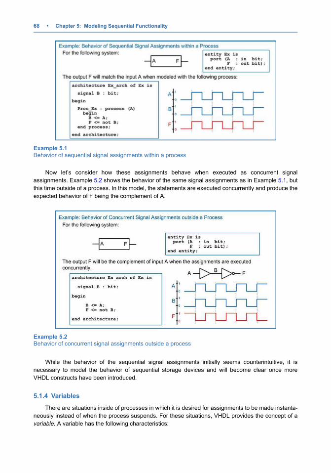
Now let’s consider how these assignments behave when executed as concurrent signal
assignments. Example 5.2 shows the behavior of the same signal assignments as in Example 5.1, but
this time outside of a process. In this model, the statements are executed concurrently and produce the
expected behavior of F being the complement of A.
While the behavior of the sequential signal assignments initially seems counterintuitive, it is
necessary to model the behavior of sequential storage devices and will become clear once more
VHDL constructs have been introduced.
5.1.4 Variables
There are situations inside of processes in which it is desired for assignments to be made instanta-
neously instead of when the process suspends. For these situations, VHDL provides the concept of a
variable. A variable has the following characteristics:
Example 5.1Behavior of sequential signal assignments within a process
Example 5.2Behavior of concurrent signal assignments outside a process
68 • Chapter 5: Modeling Sequential Functionality
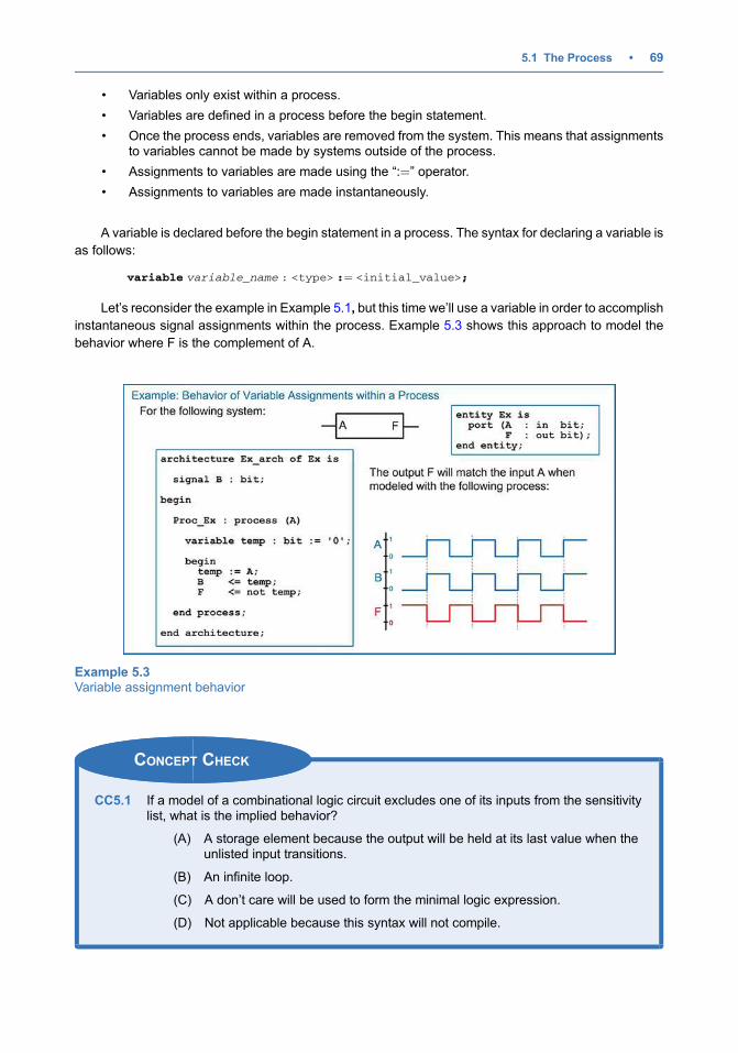
• Variables only exist within a process.
• Variables are defined in a process before the begin statement.
• Once the process ends, variables are removed from the system. This means that assignmentsto variables cannot be made by systems outside of the process.
• Assignments to variables are made using the “:¼” operator.
• Assignments to variables are made instantaneously.
A variable is declared before the begin statement in a process. The syntax for declaring a variable is
as follows:
variable variable_name : <type> :¼ <initial_value>;
Let’s reconsider the example in Example 5.1, but this time we’ll use a variable in order to accomplish
instantaneous signal assignments within the process. Example 5.3 shows this approach to model the
behavior where F is the complement of A.
CONCEPT CHECK
CC5.1 If a model of a combinational logic circuit excludes one of its inputs from the sensitivitylist, what is the implied behavior?
(A) A storage element because the output will be held at its last value when theunlisted input transitions.
(B) An infinite loop.
(C) A don’t care will be used to form the minimal logic expression.
(D) Not applicable because this syntax will not compile.
Example 5.3Variable assignment behavior
5.1 The Process • 69
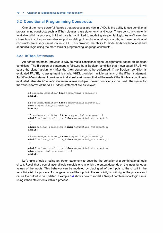
5.2 Conditional Programming Constructs
One of the more powerful features that processes provide in VHDL is the ability to use conditional
programming constructs such as if/then clauses, case statements, and loops. These constructs are only
available within a process, but their use is not limited to modeling sequential logic. As we’ll see, the
characteristics of a process also support modeling of combinational logic circuits, so these conditional
constructs are a very useful tool in VHDL. This provides the ability to model both combinational and
sequential logic using the more familiar programming language constructs.
5.2.1 If/Then Statements
An if/then statement provides a way to make conditional signal assignments based on Boolean
conditions. The if portion of statement is followed by a Boolean condition that if evaluated TRUE will
cause the signal assignment after the then statement to be performed. If the Boolean condition is
evaluated FALSE, no assignment is made. VHDL provides multiple variants of the if/then statement.
An if/then/else statement provides a final signal assignment that will be made if the Boolean condition is
evaluated false. An if/then/elsif statement allows multiple Boolean conditions to be used. The syntax for
the various forms of the VHDL if/then statement are as follows:
if boolean_condition then sequential_statementend if;
if boolean_condition then sequential_statement_1else sequential_statement_2end if;
if boolean_condition_1 then sequential_statement_1elsif boolean_condition_2 then sequential_statement_2::
elsif boolean_condition_n then sequential_statement_nend if;
if boolean_condition_1 then sequential_statement_1elsif boolean_condition_2 then sequential_statement_2::
elsif boolean_condition_n then sequential_statement_nelse sequential_statement_n+1end if;
Let’s take a look at using an if/then statement to describe the behavior of a combinational logic
circuit. Recall that a combinational logic circuit is one in which the output depends on the instantaneous
values of the inputs. This behavior can be modeled by placing all of the inputs to the circuit in the
sensitivity list of a process. A change on any of the inputs in the sensitivity list will trigger the process and
cause the output to be updated. Example 5.4 shows how to model a 3-input combinational logic circuit
using if/then statements within a process.
70 • Chapter 5: Modeling Sequential Functionality
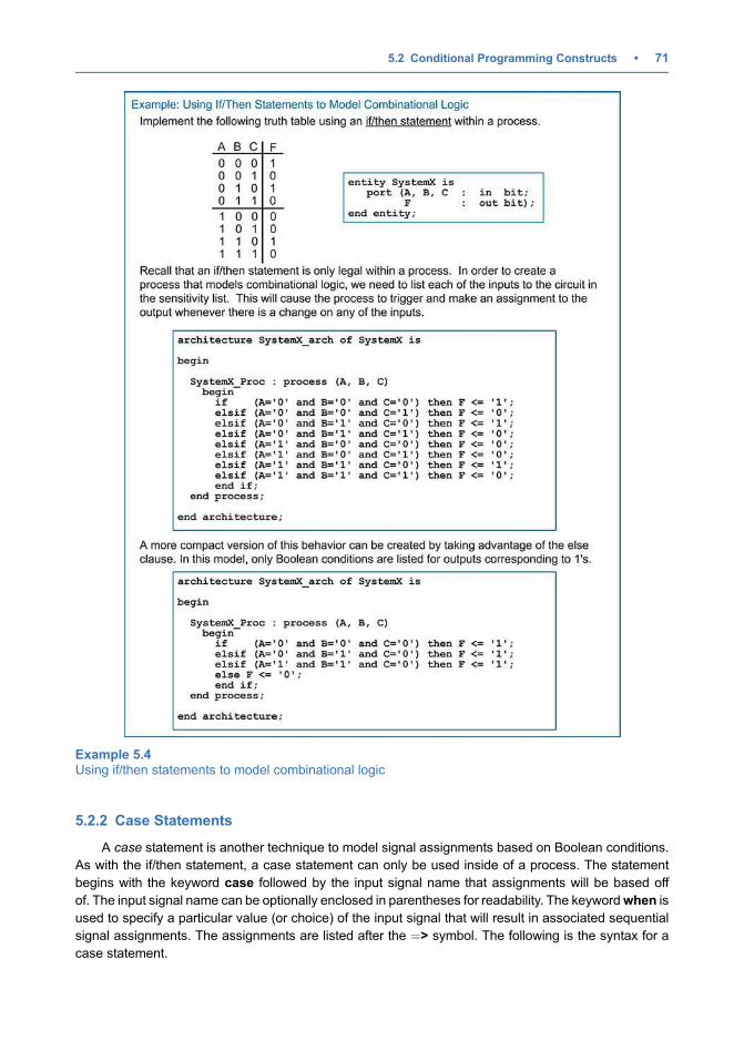
5.2.2 Case Statements
A case statement is another technique to model signal assignments based on Boolean conditions.
As with the if/then statement, a case statement can only be used inside of a process. The statement
begins with the keyword case followed by the input signal name that assignments will be based off
of. The input signal name can be optionally enclosed in parentheses for readability. The keywordwhen is
used to specify a particular value (or choice) of the input signal that will result in associated sequential
signal assignments. The assignments are listed after the ¼> symbol. The following is the syntax for a
case statement.
Example 5.4Using if/then statements to model combinational logic
5.2 Conditional Programming Constructs • 71
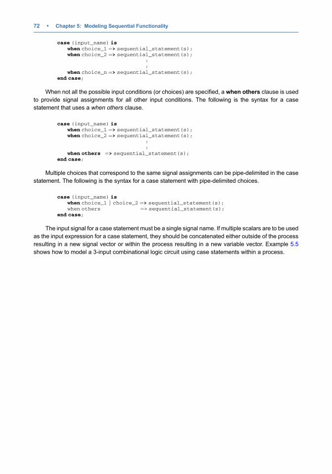
case (input_name) is
when choice_1 ¼> sequential_statement(s);when choice_2 ¼> sequential_statement(s);
::
when choice_n ¼> sequential_statement(s);end case;
When not all the possible input conditions (or choices) are specified, a when others clause is used
to provide signal assignments for all other input conditions. The following is the syntax for a case
statement that uses a when others clause.
case (input_name) is
when choice_1 ¼> sequential_statement(s);when choice_2 ¼> sequential_statement(s);
::
when others ¼> sequential_statement(s);end case;
Multiple choices that correspond to the same signal assignments can be pipe-delimited in the case
statement. The following is the syntax for a case statement with pipe-delimited choices.
case (input_name) is
when choice_1 | choice_2 ¼> sequential_statement(s);when others ¼> sequential_statement(s);
end case;
The input signal for a case statement must be a single signal name. If multiple scalars are to be used
as the input expression for a case statement, they should be concatenated either outside of the process
resulting in a new signal vector or within the process resulting in a new variable vector. Example 5.5
shows how to model a 3-input combinational logic circuit using case statements within a process.
72 • Chapter 5: Modeling Sequential Functionality
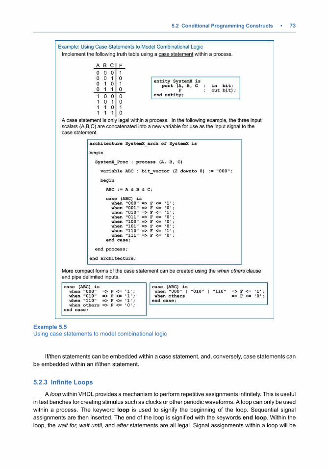
If/then statements can be embedded within a case statement, and, conversely, case statements can
be embedded within an if/then statement.
5.2.3 Infinite Loops
A loopwithin VHDL provides a mechanism to perform repetitive assignments infinitely. This is useful
in test benches for creating stimulus such as clocks or other periodic waveforms. A loop can only be used
within a process. The keyword loop is used to signify the beginning of the loop. Sequential signal
assignments are then inserted. The end of the loop is signified with the keywords end loop. Within the
loop, the wait for, wait until, and after statements are all legal. Signal assignments within a loop will be
Example 5.5Using case statements to model combinational logic
5.2 Conditional Programming Constructs • 73
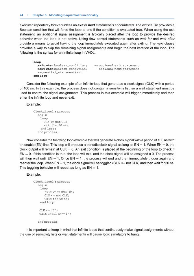
executed repeatedly forever unless an exit or next statement is encountered. The exit clause provides a
Boolean condition that will force the loop to end if the condition is evaluated true. When using the exit
statement, an additional signal assignment is typically placed after the loop to provide the desired
behavior when the loop is not active. Using flow control statements such as wait for and wait after
provide a means to avoid having the loop immediately executed again after exiting. The next clause
provides a way to skip the remaining signal assignments and begin the next iteration of the loop. The
following is the syntax for an infinite loop in VHDL.
loop
exit when boolean_condition; -- optional exit statementnext when boolean_condition; -- optional next statementsequential_statement(s);
end loop;
Consider the following example of an infinite loop that generates a clock signal (CLK) with a period
of 100 ns. In this example, the process does not contain a sensitivity list, so a wait statement must be
used to control the signal assignments. This process in this example will trigger immediately and then
enter the infinite loop and never exit.
Example:
Clock_Proc1 : processbeginloop
CLK <¼ not CLK;wait for 50 ns;
end loop;end process;
Now consider the following loop example that will generate a clock signal with a period of 100 ns with
an enable (EN) line. This loop will produce a periodic clock signal as long as EN ¼ 1. When EN ¼ 0, the
clock output will remain at CLK ¼ 0. An exit condition is placed at the beginning of the loop to check if
EN ¼ 0. If this condition is true, the loop will exit, and the clock signal will be assigned a 0. The process
will then wait until EN ¼ 1. Once EN ¼ 1, the process will end and then immediately trigger again and
reenter the loop. When EN¼ 1, the clock signal will be toggled (CLK <¼ not CLK) and then wait for 50 ns.
This toggling behavior will repeat as long as EN ¼ 1.
Example:
Clock_Proc2 : processbeginloop
exit when EN¼’0’;CLK <¼ not CLK;wait for 50 ns;
end loop;
CLK <¼ ’0’;wait until EN¼’1’;
end process;
It is important to keep in mind that infinite loops that continuously make signal assignments without
the use of sensitivity lists or wait statements will cause logic simulators to hang.
74 • Chapter 5: Modeling Sequential Functionality
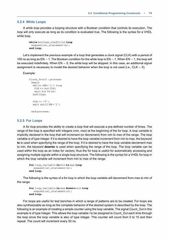
5.2.4 While Loops
A while loop provides a looping structure with a Boolean condition that controls its execution. The
loop will only execute as long as its condition is evaluated true. The following is the syntax for a VHDL
while loop.
while boolean_condition loop
sequential_statement(s);end loop;
Let’s implement the previous example of a loop that generates a clock signal (CLK) with a period of
100 ns as long as EN¼ 1. The Boolean condition for the while loop is EN¼ 1. When EN¼ 1, the loop will
be executed indefinitely. When EN ¼ 0, the while loop will be skipped. In this case, an additional signal
assignment is necessary to model the desired behavior when the loop is not used (i.e., CLK ¼ 0).
Example:
Clock_Proc3 : processbeginwhile (EN¼’1’) loopCLK <¼ not CLK;wait for 50 ns;
end loop;
CLK <¼ ’0’;wait until EN¼’1’;
end process;
5.2.5 For Loops
A for loop provides the ability to create a loop that will execute a pre-defined number of times. The
range of the loop is specified with integers (min, max) at the beginning of the for loop. A loop variable is
implicitly declared in the loop that will increment (or decrement) from min to max of the range. The loop
variable is of type integer. If it is desired to have the loop variable increment frommin to max, the keyword
to is used when specifying the range of the loop. If it is desired to have the loop variable decrement max
to min, the keyword downto is used when specifying the range of the loop. The loop variable can be
used within the loop as an index for vectors; thus the for loop is useful for automatically accessing and
assigning multiple signals within a single loop structure. The following is the syntax for a VHDL for loop in
which the loop variable will increment from min to max of the range:
for loop_variable in min to max loop
sequential_statement(s);end loop;
The following is the syntax of a for loop in which the loop variable will decrement from max to min of
the range:
for loop_variable in max downto min loop
sequential_statement(s);end loop;
For loops are useful for test benches in which a range of patterns are to be created. For loops are
also synthesizable as long as the complete behavior of the desired system is described by the loop. The
following is an example of creating a simple counter using the loop variable. The signal Count_Out in this
example is of type integer. This allows the loop variable i to be assigned to Count_Out each time through
the loop since the loop variable is also of type integer. This counter will count from 0 to 15 and then
repeat. The count will increment every 50 ns.
5.2 Conditional Programming Constructs • 75
Example:
Counter_Proc : processbegin
for i in 0 to 15 loopCount_Out <¼ i;wait for 50 ns;
end loop;end process;
CONCEPT CHECK
CC5.2 When using an if/then statement to model a combinational logic circuit, isusing the else clause the same as using don’t cares when minimizing alogic expression with a K-map?
(A) Yes. The else clause allows the synthesizer to assign whateveroutput values are necessary in order to create the most minimalcircuit.
(B) No. The else clause explicitly states the output values for all inputcodes not listed in the if/elsif portion of the if/then construct. This isthe same as filling in the truth table with specific values for all inputcodes covered by the else clause and the synthesizer will create thelogic expression accordingly.
5.3 Signal Attributes
There are situations where we want to describe behavior that is based on more than just the current
value of a signal. For example, a real D-flip-flop will only update its outputs on a particular type of
transition (i.e., rising or falling). In order to model this behavior, we need to specify more information
about the signal. This is accomplished by using attributes. Attributes provide additional information about
a signal other than just its present value. An attribute can provide information such as past values,
whether an assignment was made to a signal or when the last time an assignment resulted in a value
change. A signal attribute is implemented by placing an apostrophe (‘) after the signal name and then
listing the VHDL attribute keyword. Different attributes will result in different output types. Attributes that
yield Boolean output types can be used as inputs to Boolean decision conditions for other VHDL
constructs. Other attributes can be used to define the range of new vectors by referencing the size of
existing vectors or automatically defining the number of iterations in a loop. Finally, some attributes can
be used to create self-checking test benches that monitor the impact of circuit delays on the functionality
of a system. The following is a list of the commonly used, pre-defined VHDL signal attributes. The
example signal name A is used to illustrate how scalar attributes operate. The example signal B is used
to illustrate how vector attributes operate with type bit_vector (7 downto 0).
Attribute Information returned Type returned
A‘event True when signal A changes, false otherwise boolean
A‘active True when an assignment is made to A, false otherwise boolean
A‘last_event Time when signal A last changed time
A‘last_active Time when signal A was last assigned to time
A‘last_value The previous value of A same type as A
76 • Chapter 5: Modeling Sequential Functionality
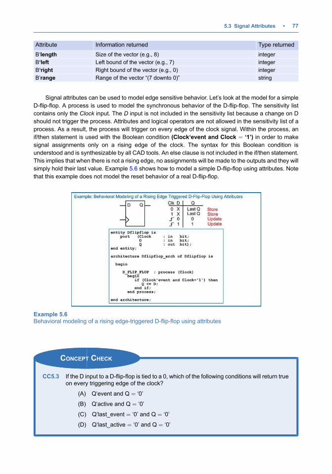
Attribute Information returned Type returned
B‘length Size of the vector (e.g., 8) integer
B‘left Left bound of the vector (e.g., 7) integer
B‘right Right bound of the vector (e.g., 0) integer
B‘range Range of the vector “(7 downto 0)” string
Signal attributes can be used to model edge sensitive behavior. Let’s look at the model for a simple
D-flip-flop. A process is used to model the synchronous behavior of the D-flip-flop. The sensitivity list
contains only the Clock input. The D input is not included in the sensitivity list because a change on D
should not trigger the process. Attributes and logical operators are not allowed in the sensitivity list of a
process. As a result, the process will trigger on every edge of the clock signal. Within the process, an
if/then statement is used with the Boolean condition (Clock‘event and Clock ¼ ‘1’) in order to make
signal assignments only on a rising edge of the clock. The syntax for this Boolean condition is
understood and is synthesizable by all CAD tools. An else clause is not included in the if/then statement.
This implies that when there is not a rising edge, no assignments will be made to the outputs and they will
simply hold their last value. Example 5.6 shows how to model a simple D-flip-flop using attributes. Note
that this example does not model the reset behavior of a real D-flip-flop.
CONCEPT CHECK
CC5.3 If the D input to a D-flip-flop is tied to a 0, which of the following conditions will return trueon every triggering edge of the clock?
(A) Q‘event and Q ¼ ‘0’
(B) Q‘active and Q ¼ ‘0’
(C) Q‘last_event ¼ ‘0’ and Q ¼ ‘0’
(D) Q‘last_active ¼ ‘0’ and Q ¼ ‘0’
Example 5.6Behavioral modeling of a rising edge-triggered D-flip-flop using attributes
5.3 Signal Attributes • 77
Summary
v To model sequential logic, an HDL needs tobe able to trigger signal assignments basedon a triggering event. This is accomplished inVHDL using a process.
v A sensitivity list is a way to control when aVHDL process is triggered. A sensitivity listcontains a list of signals. If any of the signalsin the sensitivity list transition, it will cause theprocess to trigger. If a sensitivity list is omit-ted, the process will trigger immediately.
v Signal assignments are made when a pro-cess suspends. There are two techniques tosuspend a process. The first is using the waitstatement. The second is simply ending theprocess.
v Sensitivity lists and wait statements are neverused at the same time. Sensitivity lists areused to model synthesizable logic, while waitstatements are used for test benches.
v When signal assignments are made in a pro-cess, they are made in the order they arelisted in the process. If assignments aremade to the same signal within a process,only the last assignment will take place whenthe process suspends.
v If assignments are needed to occur prior tothe process suspending, a variable is used.In VHDL, variables only exist within a pro-cess. Variables are defined when a processtriggers and deleted when the process ends.
v Processes also allow more advancedmodeling constructs in VHDL. These includeif/then statements, case statements, infiniteloops, while loops, and for loops.
v Signal attributes allow additional informationto be observed about a signal other than itsvalue.
Exercise Problems
Section 5.1: The Process
5.1.1 When using a sensitivity list in a process, whatwill cause the process to trigger?
5.1.2 When using a sensitivity list in a process, whatwill cause the process to suspend?
5.1.3 When a sensitivity list is not used in a process,when will the process trigger?
5.1.4 Can a sensitivity list and a wait statement beused in the same process at the same time?
5.1.5 Does a wait statement trigger or suspend aprocess?
5.1.6 When are signal assignments officially made ina process?
5.1.7 Why are assignments in a process calledsequential signal assignments?
5.1.8 Can signals be declared in a process?
5.1.9 Are variables declared within a process visibleto the rest of the VHDL model (e.g., are theyvisible outside of the process)?
5.1.10 What happens to a variable when a processends?
5.1.11 What is the assignment operator for variables?
Section 5.2: Conditional Programming
Constructs
5.2.1 Design a VHDLmodel to implement the behav-ior described by the 4-input truth table inFig. 5.1. Use a process and an if/then state-ment. Use std_logic and std_logic_vectortypes for your signals. Declare the entity tomatch the block diagram provided. Hint: Notice
that there are far more input codes producingF¼ 0 than producing F¼ 1. Can you use this toyour advantage to make your VHDL modelsimpler?
Fig. 5.1System I functionality
5.2.2 Design a VHDLmodel to implement the behav-ior described by the 4-input truth table inFig. 5.1. Use a process and a case statement.Use std_logic and std_logic_vector types foryour signals. Declare the entity to match theblock diagram provided.
78 • Chapter 5: Modeling Sequential Functionality
5.2.3 Design a VHDLmodel to implement the behav-ior described by the 4-input minterm list inFig. 5.2. Use a process and an if/then state-ment. Use std_logic and std_logic_vectortypes for your signals. Declare the entity tomatch the block diagram provided.
Fig. 5.2System J functionality
5.2.4 Design a VHDLmodel to implement the behav-ior described by the 4-input minterm list inFig. 5.2. Use a process and a case statement.Use std_logic and std_logic_vector types foryour signals. Declare the entity to match theblock diagram provided.
5.2.5 Design a VHDLmodel to implement the behav-ior described by the 4-input maxterm list inFig. 5.3. Use a process and an if/then state-ment. Use std_logic and std_logic_vectortypes for your signals. Declare the entity tomatch the block diagram provided.
Fig. 5.3System K functionality
5.2.6 Design a VHDLmodel to implement the behav-ior described by the 4-input maxterm list inFig. 5.3. Use a process and a case statement.Use std_logic and std_logic_vector types foryour signals. Declare the entity to match theblock diagram provided.
5.2.7 Design a VHDLmodel to implement the behav-ior described by the 4-input truth table inFig. 5.4. Use a process and an if/then state-ment. Use std_logic and std_logic_vectortypes for your signals. Declare the entity to
match the block diagram provided. Hint: Noticethat there are far more input codes producingF¼ 1 than producing F¼ 0. Can you use this toyour advantage to make your VHDL modelsimpler?
Fig. 5.4System L functionality
5.2.8 Design a VHDLmodel to implement the behav-ior described by the 4-input truth table inFig. 5.4. Use a process and a case statement.Use std_logic and std_logic_vector types foryour signals. Declare the entity to match theblock diagram provided.
Section 5.3: Signal Attributes
5.3.1 What is the purpose of a signal attribute?
5.3.2 What is the data type returned when using thesignal attribute ‘event?
5.3.3 What is the data type returned when using thesignal attribute ‘last_event?
5.3.4 What is the data type returned when using thesignal attribute ‘length?
Exercise Problems • 79
Chapter 6: PackagesOne of the drawbacks of the VHDL standard package is that it provides limited functionality in its
synthesizable data types. The bit and bit_vector, while synthesizable, lack the ability to accurately model
many of the topologies implemented in modern digital systems. Of primary interest are topologies that
involve multiple drivers connected to a single wire. The standard package will not permit this type of
connection; however, this type of topology is a common way to interface multiple nodes on a shared
interconnection. Furthermore, the standard package does not provide many useful features for these
types, such as don’t cares, arithmetic using the + and � operators, type conversion functions, or the
ability to read/write external files. To increase the functionality of VHDL, packages are included in the
design. This chapter introduces the most common packages used in modern VHDL models.
Learning Outcomes—After completing this chapter, you will be able to:
6.1 Describe the capabilities of the STD_LOGIC_1164 package that allow more accuratemodels of modern digital systems to be described.
6.2 Describe the capabilities of the NUMERIC_STD package that allow behavioral models ofarithmetic circuits to be described including operations using data types from theSTD_LOGIC_1164 package.
6.3 Describe how text reporting using external I/O can is handled by the TEXTIO andSTD_LOGIC_TEXTIO packages.
6.4 Describe the capabilities of someof the other common packages provided in the IEEE library.
6.1 STD_LOGIC_1164
In the late 1980s, the IEEE 1164 standard was released that added functionality to VHDL to allow a
multivalued logic system (i.e., a signal can take on more values than just 0 and 1). This standard also
provided a mechanism for multiple drivers to be connected to the same signal. An updated release in
1993 called IEEE 1164-1993 was the most significant update to this standard and contains the majority
of functionality used in VHDL today. Nearly all systems described in VHDL include the 1164 standard as
a package. This package is included by adding the following syntax at the beginning of the VHDL file.
library IEEE;
use IEEE.std_logic_1164.all;
This package defines four new data types: std_ulogic, std_ulogic_vector, std_logic, and
std_logic_vector. The std_ulogic and std_logic are enumerated, scalar types that can provide a
multivalued logic system. The types std_ulogic_vector and std_logic_vector are vector types containing
a linear array of scalar types std_ulogic and std_logic, respectively. The scalar types can take on nine
different values as described below.
Value Description Notes
U Uninitialized Default initial value
X Forcing unknown
0 Forcing 0
1 Forcing 1
Z High impedance
W Weak unknown
L Weak 0 Pull-down
H Weak 1 Pull-up
- Don’t care Used for synthesis only
# Springer Nature Switzerland AG 2019
B. J. LaMeres, Quick Start Guide to VHDL, https://doi.org/10.1007/978-3-030-04516-6_6
81
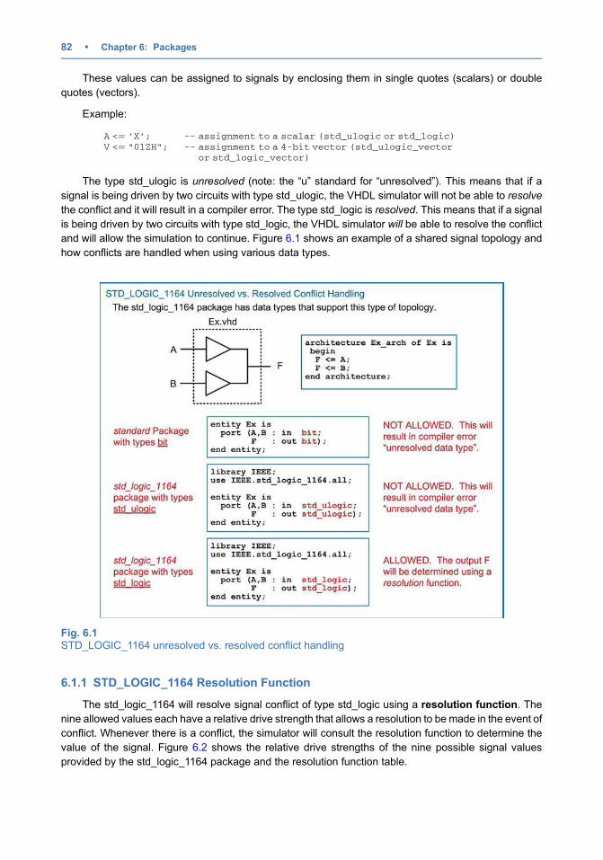
These values can be assigned to signals by enclosing them in single quotes (scalars) or double
quotes (vectors).
Example:
A <¼ ’X’; -- assignment to a scalar (std_ulogic or std_logic)
V <¼ "01ZH"; -- assignment to a 4-bit vector (std_ulogic_vector
or std_logic_vector)
The type std_ulogic is unresolved (note: the “u” standard for “unresolved”). This means that if a
signal is being driven by two circuits with type std_ulogic, the VHDL simulator will not be able to resolve
the conflict and it will result in a compiler error. The type std_logic is resolved. This means that if a signal
is being driven by two circuits with type std_logic, the VHDL simulator will be able to resolve the conflict
and will allow the simulation to continue. Figure 6.1 shows an example of a shared signal topology and
how conflicts are handled when using various data types.
6.1.1 STD_LOGIC_1164 Resolution Function
The std_logic_1164 will resolve signal conflict of type std_logic using a resolution function. The
nine allowed values each have a relative drive strength that allows a resolution to be made in the event of
conflict. Whenever there is a conflict, the simulator will consult the resolution function to determine the
value of the signal. Figure 6.2 shows the relative drive strengths of the nine possible signal values
provided by the std_logic_1164 package and the resolution function table.
Fig. 6.1STD_LOGIC_1164 unresolved vs. resolved conflict handling
82 • Chapter 6: Packages
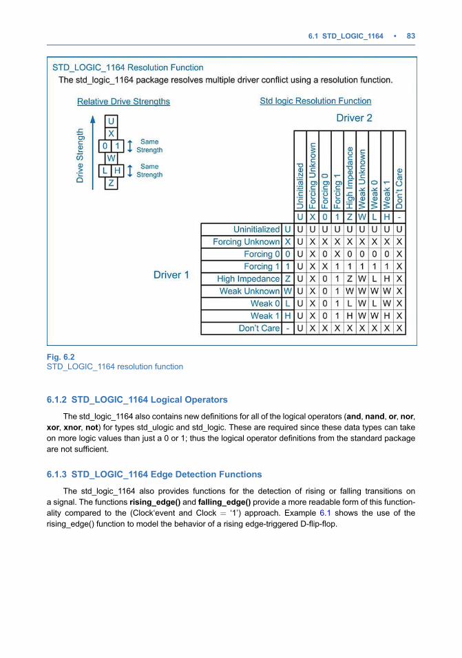
6.1.2 STD_LOGIC_1164 Logical Operators
The std_logic_1164 also contains new definitions for all of the logical operators (and, nand, or, nor,
xor, xnor, not) for types std_ulogic and std_logic. These are required since these data types can take
on more logic values than just a 0 or 1; thus the logical operator definitions from the standard package
are not sufficient.
6.1.3 STD_LOGIC_1164 Edge Detection Functions
The std_logic_1164 also provides functions for the detection of rising or falling transitions on
a signal. The functions rising_edge() and falling_edge() provide a more readable form of this function-
ality compared to the (Clock‘event and Clock ¼ ‘1’) approach. Example 6.1 shows the use of the
rising_edge() function to model the behavior of a rising edge-triggered D-flip-flop.
Fig. 6.2STD_LOGIC_1164 resolution function
6.1 STD_LOGIC_1164 • 83
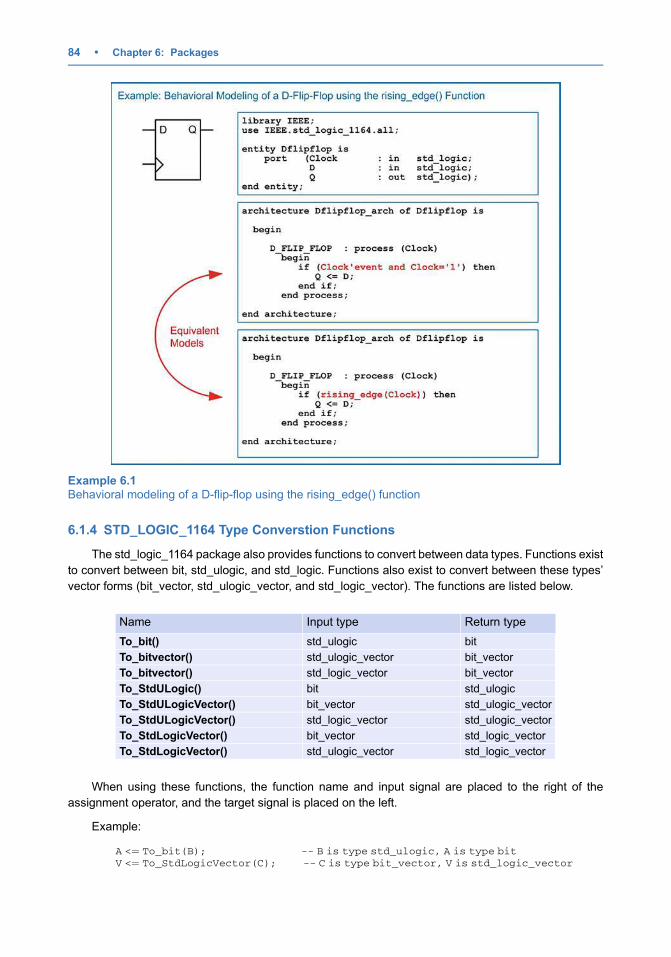
6.1.4 STD_LOGIC_1164 Type Converstion Functions
The std_logic_1164 package also provides functions to convert between data types. Functions exist
to convert between bit, std_ulogic, and std_logic. Functions also exist to convert between these types’
vector forms (bit_vector, std_ulogic_vector, and std_logic_vector). The functions are listed below.
Name Input type Return type
To_bit() std_ulogic bit
To_bitvector() std_ulogic_vector bit_vector
To_bitvector() std_logic_vector bit_vector
To_StdULogic() bit std_ulogic
To_StdULogicVector() bit_vector std_ulogic_vector
To_StdULogicVector() std_logic_vector std_ulogic_vector
To_StdLogicVector() bit_vector std_logic_vector
To_StdLogicVector() std_ulogic_vector std_logic_vector
When using these functions, the function name and input signal are placed to the right of the
assignment operator, and the target signal is placed on the left.
Example:
A <¼ To_bit(B); -- B is type std_ulogic, A is type bit
V <¼ To_StdLogicVector(C); -- C is type bit_vector, V is std_logic_vector
Example 6.1Behavioral modeling of a D-flip-flop using the rising_edge() function
84 • Chapter 6: Packages
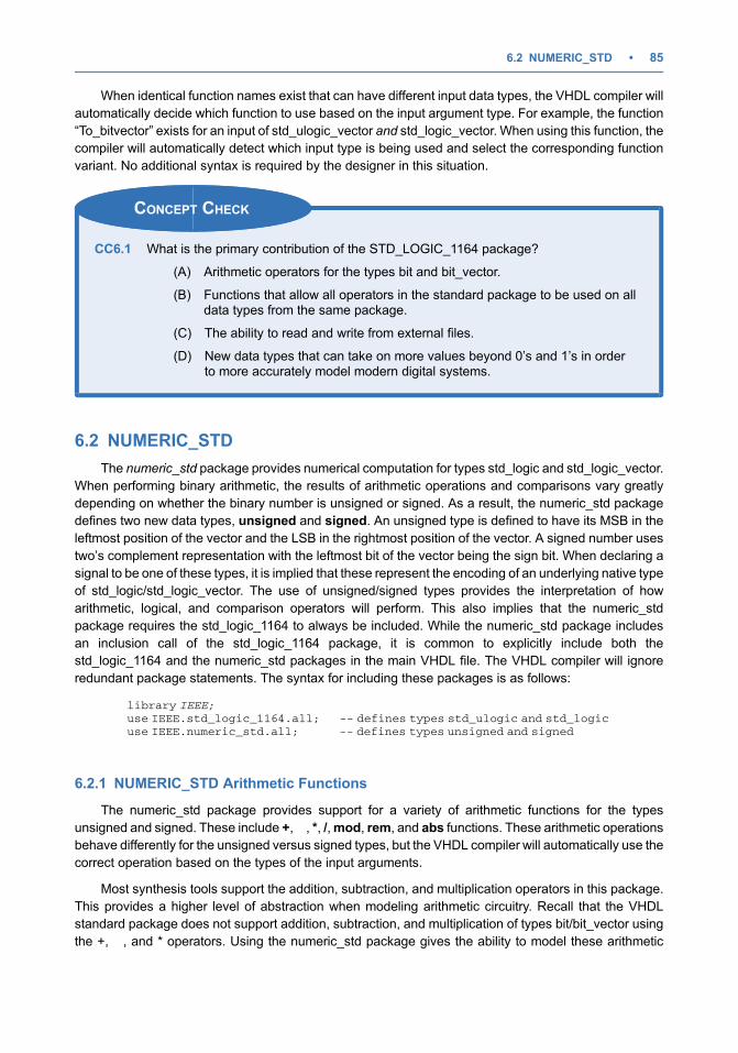
When identical function names exist that can have different input data types, the VHDL compiler will
automatically decide which function to use based on the input argument type. For example, the function
“To_bitvector” exists for an input of std_ulogic_vector and std_logic_vector. When using this function, the
compiler will automatically detect which input type is being used and select the corresponding function
variant. No additional syntax is required by the designer in this situation.
CONCEPT CHECK
CC6.1 What is the primary contribution of the STD_LOGIC_1164 package?
(A) Arithmetic operators for the types bit and bit_vector.
(B) Functions that allow all operators in the standard package to be used on alldata types from the same package.
(C) The ability to read and write from external files.
(D) New data types that can take on more values beyond 0’s and 1’s in orderto more accurately model modern digital systems.
6.2 NUMERIC_STD
The numeric_std package provides numerical computation for types std_logic and std_logic_vector.
When performing binary arithmetic, the results of arithmetic operations and comparisons vary greatly
depending on whether the binary number is unsigned or signed. As a result, the numeric_std package
defines two new data types, unsigned and signed. An unsigned type is defined to have its MSB in the
leftmost position of the vector and the LSB in the rightmost position of the vector. A signed number uses
two’s complement representation with the leftmost bit of the vector being the sign bit. When declaring a
signal to be one of these types, it is implied that these represent the encoding of an underlying native type
of std_logic/std_logic_vector. The use of unsigned/signed types provides the interpretation of how
arithmetic, logical, and comparison operators will perform. This also implies that the numeric_std
package requires the std_logic_1164 to always be included. While the numeric_std package includes
an inclusion call of the std_logic_1164 package, it is common to explicitly include both the
std_logic_1164 and the numeric_std packages in the main VHDL file. The VHDL compiler will ignore
redundant package statements. The syntax for including these packages is as follows:
library IEEE;
use IEEE.std_logic_1164.all; -- defines types std_ulogic and std_logic
use IEEE.numeric_std.all; -- defines types unsigned and signed
6.2.1 NUMERIC_STD Arithmetic Functions
The numeric_std package provides support for a variety of arithmetic functions for the types
unsigned and signed. These include +,�, *, /,mod, rem, and abs functions. These arithmetic operations
behave differently for the unsigned versus signed types, but the VHDL compiler will automatically use the
correct operation based on the types of the input arguments.
Most synthesis tools support the addition, subtraction, and multiplication operators in this package.
This provides a higher level of abstraction when modeling arithmetic circuitry. Recall that the VHDL
standard package does not support addition, subtraction, and multiplication of types bit/bit_vector using
the +, �, and * operators. Using the numeric_std package gives the ability to model these arithmetic
6.2 NUMERIC_STD • 85
operations with a synthesizable data type using the more familiar mathematical operators. The division,
modulo, remainder, and absolute value functions are not synthesizable directly from this package.
Example:
F <¼ A + B; -- A, B, F are type unsigned(3 downto 0)
F <¼ A - B;
The numeric_std package gives the ability to model arithmetic at a higher level of abstraction. Let’s
look at an example of implementing an adder circuit using the “+” operator. While this operator is
supported for the type integer in the std_logic_1164 package, modeling adders using integers can be
onerous due to the multiple levels of casting, range checking, and manual handling of carry out. A
simpler approach to modeling adder behavior is to use the types unsigned/signed and the “+” operator
provided in the numeric_std package. Temporary signals or variables of these types are required to
model the adder behavior with the “+” sign. Also, type casting is still required when assigning the values
back to the output ports. One advantage of this approach is that range checking is eliminated because
rollover is automatically handled with these types.
Example 6.2 shows a behavioral model for a 4-bit adder in VHDL. In this model, a 5-bit unsigned
vector is created (Sum_uns). The two inputs, A and B, are concatenated with a leading zero in order to
facilitate assigning the sum to this 5-bit vector. The advantage of this approach is that the carry out of the
adder is automatically included in the sum as the highest position bit. Since A and B are of type
std_logic_vector, they must be converted to unsigned before the addition with the “+” operator can
take place. The concatenation, type conversion, and addition can all take place in a single assignment.
Example:
Sum_uns <¼ unsigned((’0’ & A)) + unsigned((’0’ & B));
The 5-bit vector Sum_uns now contains the 4-bit sum and carry out. The final step is to assign the
separate components of this vector to the output ports of the system. The 4-bit sum portion requires a
type conversion back to std_logic_vector before it can be assigned to the output port Sum. Since the
Cout port is a scalar, an unsigned signal can be assigned to it directly without the need for a conversion.
Example:
Sum <¼ std_logic_vector(Sum_uns(3 downto 0));
Cout <¼ Sum_uns(4);
86 • Chapter 6: Packages
6.2.2 NUMERIC_STD Logical Functions
The numeric_std package provides support for all of the logical operators (and, nand, or, nor, xor,
xnor, not) for types unsigned and signed. It also provides two new shift functions shift_left() and
shift_right(). These shift functions will fill the vacant position in the vector after the shift with a 0; thus
these are logical shifts. This package also provides two new rotate functions rotate_left() and
rotate_right().
6.2.3 NUMERIC_STD Comparison Functions
The numeric_std package provides support for all of the comparison functions for types unsigned
and signed. These include >, <, <¼, >¼, ¼, and /¼. These comparisons return type Boolean.
Example: (A ¼ “0000”, B ¼ “1111”).
if (A < B) then -- This condition is TRUE if A and B are UNSIGNED
:
if (A < B) then -- This condition is FALSE if A and B are SIGNED
6.2.4 NUMERIC_STD Edge Detection Functions
The numeric_std also provides the functions rising_edge() and falling_edge() for the detection of
rising or falling edge transition detection for types unsigned and signed.
Example 6.2Behavioral model of a 4-bit adder in VHDL
6.2 NUMERIC_STD • 87
6.2.5 NUMERIC_STD Conversion Functions
The numeric_std package contains a variety of useful conversion functions. Of particular usefulness
are functions between the type integer and to/from unsigned/signed. This allows behavioral models for
counters, adders, and subtractors to be implemented using the more readable type integer. After the
functionality has been described, a conversion can be used to turn the result into types unsigned or
signed to provide a synthesizable output. When converting an integer to a vector, a size argument is
included. The size argument is of type integer and provides the number of bits in the vector that the
integer will be converted to.
Name Input type Return type
To_integer() unsigned integer
To_integer() signed integer
To_unsigned() integer, <size> unsigned (size-1 downto 0)
To_signed() integer, <size> signed (size-1 downto 0)
6.2.6 NUMERIC_STD Type Casting
VHDL contains a set of built-in type casting operations that are commonly used with the numeric_std
package to convert between std_logic_vector and unsigned/signed. Since the types unsigned and
signed are based on the underlying type std_logic_vector, the conversion is simply known as casting.
The following are the built-in type casting capabilities in VHDL.
Name Input type Return type
std_logic_vector() unsigned std_logic_vector
std_logic_vector() signed std_logic_vector
unsigned() std_logic_vector unsigned
signed() std_logic_vector signed
When using these type casts, they are placed on the right-hand side of the assignment exactly as a
conversion function.
Example:
A <¼ std_logic_vector(B); -- B is unsigned, A is std_logic_vector
C <¼ unsigned(D); -- D is std_logic_vector, C is unsigned
Type casts and conversion functions can be compounded in order to perform multiple conversions
in one assignment. This is useful when converting between types that do not have a direct cast or
conversion function. Let’s look at the example of converting an integer to an 8-bit std_logic_vector where
the number being represented is unsigned. The first step is to convert the integer to an unsigned type.
This can be accomplished with the to_unsigned function defined in the numeric_std package. This can
be embedded in a second cast from unsigned to std_logic_vector. In the following example, E is the
target of the operation and is of type std_logic vector. F is the argument of assignment and is of type
integer. Recall that the to_unsigned conversions require both the input integer name and the size of the
unsigned vector being converted to.
Example:
E <¼ std_logic_vector(to_unsigned(F, 8));
88 • Chapter 6: Packages
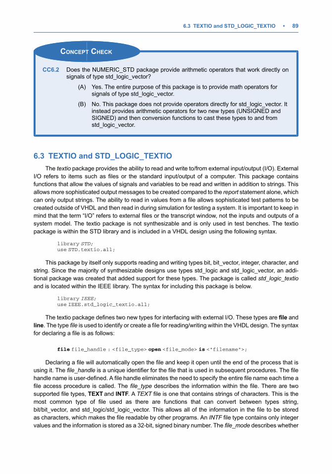
CONCEPT CHECK
CC6.2 Does the NUMERIC_STD package provide arithmetic operators that work directly onsignals of type std_logic_vector?
(A) Yes. The entire purpose of this package is to provide math operators forsignals of type std_logic_vector.
(B) No. This package does not provide operators directly for std_logic_vector. Itinstead provides arithmetic operators for two new types (UNSIGNED andSIGNED) and then conversion functions to cast these types to and fromstd_logic_vector.
6.3 TEXTIO and STD_LOGIC_TEXTIO
The textio package provides the ability to read and write to/from external input/output (I/O). External
I/O refers to items such as files or the standard input/output of a computer. This package contains
functions that allow the values of signals and variables to be read and written in addition to strings. This
allowsmore sophisticated output messages to be created compared to the report statement alone, which
can only output strings. The ability to read in values from a file allows sophisticated test patterns to be
created outside of VHDL and then read in during simulation for testing a system. It is important to keep in
mind that the term “I/O” refers to external files or the transcript window, not the inputs and outputs of a
system model. The textio package is not synthesizable and is only used in test benches. The textio
package is within the STD library and is included in a VHDL design using the following syntax.
library STD;
use STD.textio.all;
This package by itself only supports reading and writing types bit, bit_vector, integer, character, and
string. Since the majority of synthesizable designs use types std_logic and std_logic_vector, an addi-
tional package was created that added support for these types. The package is called std_logic_textio
and is located within the IEEE library. The syntax for including this package is below.
library IEEE;
use IEEE.std_logic_textio.all;
The textio package defines two new types for interfacing with external I/O. These types are file and
line. The type file is used to identify or create a file for reading/writing within the VHDL design. The syntax
for declaring a file is as follows:
file file_handle : <file_type> open <file_mode> is <"filename">;
Declaring a file will automatically open the file and keep it open until the end of the process that is
using it. The file_handle is a unique identifier for the file that is used in subsequent procedures. The file
handle name is user-defined. A file handle eliminates the need to specify the entire file name each time a
file access procedure is called. The file_type describes the information within the file. There are two
supported file types, TEXT and INTF. A TEXT file is one that contains strings of characters. This is the
most common type of file used as there are functions that can convert between types string,
bit/bit_vector, and std_logic/std_logic_vector. This allows all of the information in the file to be stored
as characters, which makes the file readable by other programs. An INTF file type contains only integer
values and the information is stored as a 32-bit, signed binary number. The file_mode describes whether
6.3 TEXTIO and STD_LOGIC_TEXTIO • 89
the file will be read from or written to. There are two supported modes, WRITE_MODE and
READ_MODE. The filename is given within double quotes and is user-defined. It is common to enter
an extension on the file so that it can be opened by other programs (e.g., output.txt). Declaring a file
always takes place within a process before the process begin statement. The following are examples of
how to declare files.
file Fout: TEXT open WRITE_MODE is "output_file.txt";
file Fin: TEXT open READ_MODE is "input_file.txt";
The information within a file is accessed (either read or written) using the concept of a line. In the
textio package, a file is interpreted as a sequence of lines, each containing either a string of characters or
an integer value. The type line is used as a temporary buffer when accessing a line within the file. When
accessing a file, a variable is created of type line. This variable is then used to either hold information that
is read from a line in the file or to hold the information that is to be written to a line in the file. A variable is
necessary for this behavior since assignments to/from the file must be made immediately. As such, a line
variable is always declared within a process before the process begin statement. The syntax for
declaring a variable of type line is as follows:
variable <line_variable_name> : line;
There are two procedures that allow information to be transferred between a line variable in VHDL
and a line in a file. These procedures are readline() and writeline(). Their syntax is as follows:
readline(<file_handle>, <line_variable_name>);
writeline(<file_handle>, <line_variable_name>);
The transfer of information between a line variable and a line in a file using these procedures is
accomplished on the entire line. There is no mechanism to read or write only a portion of the line in a file.
Once a file is opened/created using a file declaration, the lines are accessed in the order they appear in
the file. The first procedure called (either readline() or writeline()) will access the first line of the file. The
next time a procedure is called, it will access the second line of the file. This will continue until all of the
lines have been accessed. The textio package provides a function to indicate when the end of the file has
been reached when performing a readline(). This function is called endfile() and returns type Boolean.
This function will return true once the end of the file has been reached. Figure 6.3 shows a graphical
representation of how the textio package handles external file access.
90 • Chapter 6: Packages
Two additional procedures are provided to add or retrieve information to/from the line variable within
the VHDL test bench. These procedures are read() and write(). The syntax for these procedures is as
follows:
read(<line_variable_name>, <destination_variable>);
write(<line_variable_name>, <source_variable>);
When using the read() procedure, the information in the line variable is treated as space-delimited.
This means that each read() procedure will retrieve the information from the line variable until it reaches a
white space. This allows multiple read() procedures to be used in order to parse the information into
separate destination_variable names. The destination_variable must be of the appropriate type and size
of the information being read from the file. For example, if the field in the line being read is a 4-character
string (“wxyz”), then a destination variable must be defined of type string(1 to 4). If the field being read is a
2-bit std_logic_vector, then a destination variable must be defined of type std_logic_vector(1 downto 0).
The read() procedure will ignore the delimiting white space character.
When using the write() procedure, the source_destination is assumed to be of type bit, bit_vector,
integer, std_logic, or std_logic_vector. If it is desired to enter a text string directly, then the function string
is used with the format string’ <“characters. . .”>. Multiple write() procedures can be used to insert
information into the line variable. Each subsequent write procedure appends the information to the
end of the string. This allows different types of information to be interleaved (e.g., text, signal value, text,
etc.).
Fig. 6.3IEEE.textio package interpretation of files
6.3 TEXTIO and STD_LOGIC_TEXTIO • 91
CONCEPT CHECK
CC6.3 What is the primary functionality that is provided when using the TEXTIO andSTD_LOGIC_TEXTIO packages?
(A) Arithmetic operators for the types bit and bit_vector.
(B) Functions that allow all operators in the standard package to be used on alldata types from the same package.
(C) The ability to read and write from external files.
(D) New data types that can take on more values beyond 0’s and 1’s in order tomore accurately model modern digital systems.
6.4 Other Common Packages
6.4.1 NUMERIC_STD_UNSIGNED
When using the numeric_std package, the data types unsigned and signed must be used in order to
get access to the numeric operators. While this provides ultimate control over the behavior of the signal
operations and comparisons, many designs may only use unsigned types. In order to provide a
mechanism to treat all vectors as unsigned while leaving their type as std_logic_vector, the numeric_st-
d_unsigned package was created. When this package is used, it will treat all std_logic_vectors in the
design as unsigned. This package requires the std_logic_1164 and numeric_std packages to be
previously included. When used, all signals and ports can be declared as std_logic/std_logic_vector,
and they will be treated as unsigned when performing arithmetic operations and comparisons. The
following is an example of how to include this package.
library IEEE;
use IEEE.std_logic_1164.all;
use IEEE.numeric_std.all;
use IEEE.numeric_std_unsigned.all;
The numeric_std_unsigned package contains a fewmore type conversions beyond the numeric_std
package. These additional conversions are as follows:
Name Input type Return type
To_Integer std_logic_vector integer
To_StdLogicVector unsigned std_logic_vector
6.4.2 NUMERIC_BIT
The numeric_bit package provides numerical computation for types bit and bit_vector. Since the
vast majority of VHDL designs today use types std_logic and std_logic_vector instead of bit/bit_vector,
this package is rarely used. This package is included by adding the following syntax at the beginning of
the VHDL file in the design.
library IEEE;
use IEEE.numeric_bit.all; -- defines types unsigned and signed
92 • Chapter 6: Packages
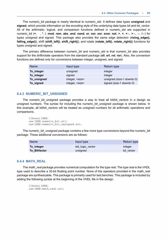
The numeric_bit package is nearly identical to numeric_std. It defines data types unsigned and
signed, which provide information on the encoding style of the underlying data types bit and bit_vector.
All of the arithmetic, logical, and comparison functions defined in numeric_std are supported in
numeric_bit (+, �, *, /, mod, rem, abs, and, nand, or, nor, xor, xnor, not, >, <, <¼, >¼, ¼, /¼) for
types unsigned and signed. This package also provides the same edge detection (rising_edge(),
falling_edge()), shift (shift_left(), shift_right()), and rotate (rotate_left(), rotate_right()) functions for
types unsigned and signed.
The primary difference between numeric_bit and numeric_std is that numeric_bit also provides
support for the shift/rotate operators from the standard package (sll, srl, rol, ror). Also, the conversion
functions are defined only for conversions between integer, unsigned, and signed.
Name Input type Return type
To_integer unsigned integer
To_integer signed integer
To_unsigned integer, <size> unsigned (size-1 downto 0)
To_signed integer, <size> signed (size-1 downto 0)
6.4.3 NUMERIC_BIT_UNSIGNED
The numeric_bit_unsigned package provides a way to treat all bit/bit_vectors in a design as
unsigned numbers. The syntax for including the numeric_bit_unsigned package is shown below. In
this example, all bit/bit_vectors will be treated as unsigned numbers for all arithmetic operations and
comparisons.
library IEEE;
use IEEE.numeric_bit.all;
use IEEE.numeric_bit_unsigned.all;
The numeric_bit_unsigned package contains a few more type conversions beyond the numeric_bit
package. These additional conversions are as follows:
Name Input type Return type
To_integer std_logic_vector integer
To_BitVector unsigned bit_vector
6.4.4 MATH_REAL
Themath_real package provides numerical computation for the type real. The type real is the VHDL
type used to describe a 32-bit floating point number. None of the operators provided in the math_real
package are synthesizable. This package is primarily used for test benches. This package is included by
adding the following syntax at the beginning of the VHDL file in the design.
library IEEE;
use IEEE.math_real.all;
6.4 Other Common Packages • 93
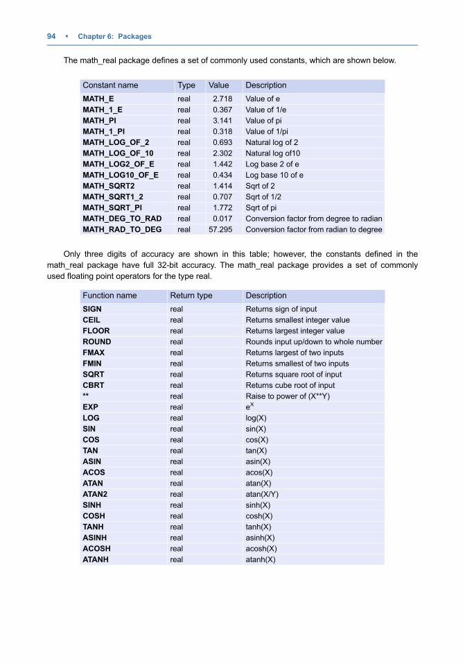
The math_real package defines a set of commonly used constants, which are shown below.
Constant name Type Value Description
MATH_E real 2.718 Value of e
MATH_1_E real 0.367 Value of 1/e
MATH_PI real 3.141 Value of pi
MATH_1_PI real 0.318 Value of 1/pi
MATH_LOG_OF_2 real 0.693 Natural log of 2
MATH_LOG_OF_10 real 2.302 Natural log of10
MATH_LOG2_OF_E real 1.442 Log base 2 of e
MATH_LOG10_OF_E real 0.434 Log base 10 of e
MATH_SQRT2 real 1.414 Sqrt of 2
MATH_SQRT1_2 real 0.707 Sqrt of 1/2
MATH_SQRT_PI real 1.772 Sqrt of pi
MATH_DEG_TO_RAD real 0.017 Conversion factor from degree to radian
MATH_RAD_TO_DEG real 57.295 Conversion factor from radian to degree
Only three digits of accuracy are shown in this table; however, the constants defined in the
math_real package have full 32-bit accuracy. The math_real package provides a set of commonly
used floating point operators for the type real.
Function name Return type Description
SIGN real Returns sign of input
CEIL real Returns smallest integer value
FLOOR real Returns largest integer value
ROUND real Rounds input up/down to whole number
FMAX real Returns largest of two inputs
FMIN real Returns smallest of two inputs
SQRT real Returns square root of input
CBRT real Returns cube root of input
** real Raise to power of (X**Y)
EXP real eX
LOG real log(X)
SIN real sin(X)
COS real cos(X)
TAN real tan(X)
ASIN real asin(X)
ACOS real acos(X)
ATAN real atan(X)
ATAN2 real atan(X/Y)
SINH real sinh(X)
COSH real cosh(X)
TANH real tanh(X)
ASINH real asinh(X)
ACOSH real acosh(X)
ATANH real atanh(X)
94 • Chapter 6: Packages
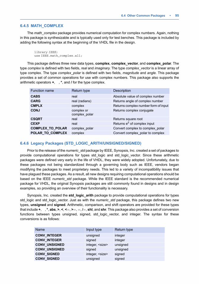
6.4.5 MATH_COMPLEX
The math_complex package provides numerical computation for complex numbers. Again, nothing
in this package is synthesizable and is typically used only for test benches. This package is included by
adding the following syntax at the beginning of the VHDL file in the design.
library IEEE;
use IEEE.math_complex.all;
This package defines three new data types, complex, complex_vector, and complex_polar. The
type complex is defined with two fields, real and imaginary. The type complex_vector is a linear array of
type complex. The type complex_polar is defined with two fields, magnitude and angle. This package
provides a set of common operations for use with complex numbers. This package also supports the
arithmetic operators +, �, *, and / for the type complex.
Function name Return type Description
CABS real Absolute value of complex number
CARG real (radians) Returns angle of complex number
CMPLX complex Returns complex number form of input
CONJ complex or
complex_polar
Returns complex conjugate
CSQRT real Returns square root
CEXP real Returns eZ of complex input
COMPLEX_TO_POLAR complex_polar Convert complex to complex_polar
POLAR_TO_COMPLEX complex Convert complex_polar to complex
6.4.6 Legacy Packages (STD_LOGIC_ARITH/UNSIGNED/SIGNED)
Prior to the release of the numeric_std package by IEEE, Synopsis, Inc. created a set of packages to
provide computational operations for types std_logic and std_logic_vector. Since these arithmetic
packages were defined very early in the life of VHDL, they were widely adopted. Unfortunately, due to
these packages not being standardized through a governing body such as IEEE, vendors began
modifying the packages to meet proprietary needs. This led to a variety of incompatibility issues that
have plagued these packages. As a result, all new designs requiring computational operations should be
based on the IEEE numeric_std package. While the IEEE standard is the recommended numerical
package for VHDL, the original Synopsis packages are still commonly found in designs and in design
examples, so providing an overview of their functionality is necessary.
Synopsis, Inc. created the std_logic_arith package to provide computational operations for types
std_logic and std_logic_vector. Just as with the numeric_std package, this package defines two new
types, unsigned and signed. Arithmetic, comparison, and shift operators are provided for these types
that include +,�, *, abs, >, <, <¼, >¼,¼, /¼, shl, and shr. This package also provides a set of conversion
functions between types unsigned, signed, std_logic_vector, and integer. The syntax for these
conversions is as follows:
Name Input type Return type
CONV_INTEGER unsigned integer
CONV_INTEGER signed integer
CONV_UNSIGNED integer, <size> unsigned
CONV_UNSIGNED signed unsigned
CONV_SIGNED integer, <size> signed
CONV_SIGNED unsigned signed
6.4 Other Common Packages • 95
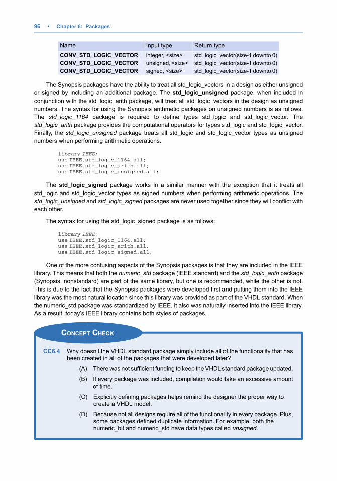
Name Input type Return type
CONV_STD_LOGIC_VECTOR integer, <size> std_logic_vector(size-1 downto 0)
CONV_STD_LOGIC_VECTOR unsigned, <size> std_logic_vector(size-1 downto 0)
CONV_STD_LOGIC_VECTOR signed, <size> std_logic_vector(size-1 downto 0)
The Synopsis packages have the ability to treat all std_logic_vectors in a design as either unsigned
or signed by including an additional package. The std_logic_unsigned package, when included in
conjunction with the std_logic_arith package, will treat all std_logic_vectors in the design as unsigned
numbers. The syntax for using the Synopsis arithmetic packages on unsigned numbers is as follows.
The std_logic_1164 package is required to define types std_logic and std_logic_vector. The
std_logic_arith package provides the computational operators for types std_logic and std_logic_vector.
Finally, the std_logic_unsigned package treats all std_logic and std_logic_vector types as unsigned
numbers when performing arithmetic operations.
library IEEE;
use IEEE.std_logic_1164.all;
use IEEE.std_logic_arith.all;
use IEEE.std_logic_unsigned.all;
The std_logic_signed package works in a similar manner with the exception that it treats all
std_logic and std_logic_vector types as signed numbers when performing arithmetic operations. The
std_logic_unsigned and std_logic_signed packages are never used together since they will conflict with
each other.
The syntax for using the std_logic_signed package is as follows:
library IEEE;
use IEEE.std_logic_1164.all;
use IEEE.std_logic_arith.all;
use IEEE.std_logic_signed.all;
One of the more confusing aspects of the Synopsis packages is that they are included in the IEEE
library. This means that both the numeric_std package (IEEE standard) and the std_logic_arith package
(Synopsis, nonstandard) are part of the same library, but one is recommended, while the other is not.
This is due to the fact that the Synopsis packages were developed first and putting them into the IEEE
library was the most natural location since this library was provided as part of the VHDL standard. When
the numeric_std package was standardized by IEEE, it also was naturally inserted into the IEEE library.
As a result, today’s IEEE library contains both styles of packages.
CONCEPT CHECK
CC6.4 Why doesn’t the VHDL standard package simply include all of the functionality that hasbeen created in all of the packages that were developed later?
(A) Therewas not sufficient funding to keep the VHDL standard package updated.
(B) If every package was included, compilation would take an excessive amountof time.
(C) Explicitly defining packages helps remind the designer the proper way tocreate a VHDL model.
(D) Because not all designs require all of the functionality in every package. Plus,some packages defined duplicate information. For example, both thenumeric_bit and numeric_std have data types called unsigned.
96 • Chapter 6: Packages
Summary
v The IEEE STD_LOGIC_1164 packageprovidesmore realistic data types formodelingmodern digital systems. This packageprovides the std_ulogic and std_logic datatypes. These data types can take on nine dif-ferent values (U, X, 0, 1, Z, W, L, H, and -).
v The std_logic data type provides a resolutionfunction that allows multiple outputs to beconnected to the same signal. The resolutionfunction will determine the value of the signalbased on a pre-defined priority given in thefunction.
v The IEEE STD_LOGIC_1164 packageprovides logical operators and edge detec-tion functions for the types std_ulogic andstd_logic. It also provides conversionfunctions to and from the type bit.
v The IEEE NUMERIC_STD packageprovides the data types unsigned andsigned. These types use the underlyingdata type std_logic. These types provide theability to treat vectors as either unsigned ortwo’s complement codes.
v The IEEE NUMERIC_STD packageprovides arithmetic operations for the typesunsigned and signed. This package alsoprovides conversions functions and typecasts to and from the types integer andstd_logic_vector.
v The TEXTIO and STD_LOGIC_TEXTIOpackages provide the functionality to readand write to external files.
Exercise Problems
Section 6.1: STD_LOGIC_1164
6.1.1 What are all the possible values that a signal oftype std_logic can take on?
6.1.2 What is the difference between the typesstd_ulogic and std_logic?
6.1.3 If a signal of type std_logic is assigned both a0 and Z at the same time, what will the finalsignal value be?
6.1.4 If a signal of type std_logic is assigned both a1 and X at the same time, what will the finalsignal value be?
6.1.5 If a signal of type std_logic is assigned both a0 and L at the same time, what will the finalsignal value be?
6.1.6 Are any arithmetic operations provided for thetype std_logic_vector in theSTD_LOGIC_1164 package?
Section 6.2: NUMERIC_STD
6.2.1 If you declare a signal of type unsigned fromthe NUMERIC_STD package, what are all thepossible values that the signal can take on?
6.2.2 If you declare a signal of type signed from theNUMERIC_STD package, what are all the pos-sible values that the signal can take on?
6.2.3 If two signals (A and B) are declared of typesigned from the NUMERIC_STD package andhold the values A <¼ “1111” and B <¼ “0000”,which signal has a greater value?
6.2.4 If two signals (A and B) are declared of typeunsigned from the NUMERIC_STD package
and hold the values A <¼ “1111” andB <¼ “0000”, which signal has a greater value?
6.2.5 If you are using the NUMERIC_STD package,what is the syntax to convert a signal of typeunsigned into std_logic_vector?
6.2.6 If you are using the NUMERIC_STD package,what is the syntax to convert a signal of typeinteger into std_logic_vector?
Section 6.3: TEXTIO and STD_LOGIC_
TEXTIO
6.3.1 What does the keyword file accomplish?
6.3.2 What is the difference between the commandswrite and writeline?
6.3.3 Can two different types of information be writ-ten to a line variable in one command?
6.3.4 What is the name of the special file handlereserved for the standard output of acomputer?
Section 6.4: Other Common Packages
6.4.1 What is the impact of including theNUMERIC_STD_UNSIGNED package?
6.4.2 Does the NUMERIC-BIT package supportresolved data types?
6.4.3 Are the functions in the MATH_REAL andMATH_COMPLEX package synthesizable?
6.4.4 Can the NUMERIC_STD andSTD_LOGIC_ARITH packages be used atthe same time? Explain why or why not?
Exercise Problems • 97
Chapter 7: Test BenchesThe functional verification of VHDL designs is accomplished through simulation using a test bench.
A test bench is a VHDL system that instantiates the system to be tested as a component and then
generates the input patterns and observes the outputs. VHDL provides a variety of capability to design
test benches that can automate stimulus generation and provide automated output checking. These
capabilities can be expanded by including packages that take advantage of reading/writing to external
I/O. This chapter provides the details of VHDL’s built-in capabilities that allow test benches to be created
and some examples of automated stimulus generation and using external files.
Learning Outcomes—After completing this chapter, you will be able to:
7.1 Design a VHDL test bench that manually creates each stimulus pattern using a series ofsignal assignments and wait statements within a process.
7.2 Design a VHDL test bench that uses for loops to automatically generate an exhaustive setof stimulus patterns.
7.3 Design a VHDL test bench that automatically checks the outputs of the system beingtested using report and assert statements.
7.4 Design a VHDL test bench that uses external I/O as part of the testing proceduresincluding reading stimulus patterns from, and writing the results to, external files.
7.1 Test Bench Overview
Creating the testing strategy for a design is a critical piece of the digital design process. In
HDL-based testing, the system being tested is often called a device under test (DUT) or unit under
test (UUT). Test benches are only used for simulation so we can use abstract modeling techniques that
are unsynthesizable to generate the stimulus patterns. VHDL also contains specific functionality to report
on the status of a test and also automatically check that the outputs are correct. Example 7.1 shows how
to create a simple test bench to verify the operation of SystemX. The test bench does not have any inputs
or outputs; thus there are no ports declared in the entity. SystemX is declared as a component in the test
bench and then instantiated (DUT1). Internal signals are declared to connect to the component under
test (A_TB, B_TB, C_TB, F_TB). A process is then used to drive the inputs of SystemX. Within the
process, wait statements are used to control the execution of the signal assignments; thus the process
does not have a sensitivity list. Each possible input code is generated within the process. The output
(F_TB) is observed using a simulation tool in either the form of a waveform or a table listing.
# Springer Nature Switzerland AG 2019
B. J. LaMeres, Quick Start Guide to VHDL, https://doi.org/10.1007/978-3-030-04516-6_7
99
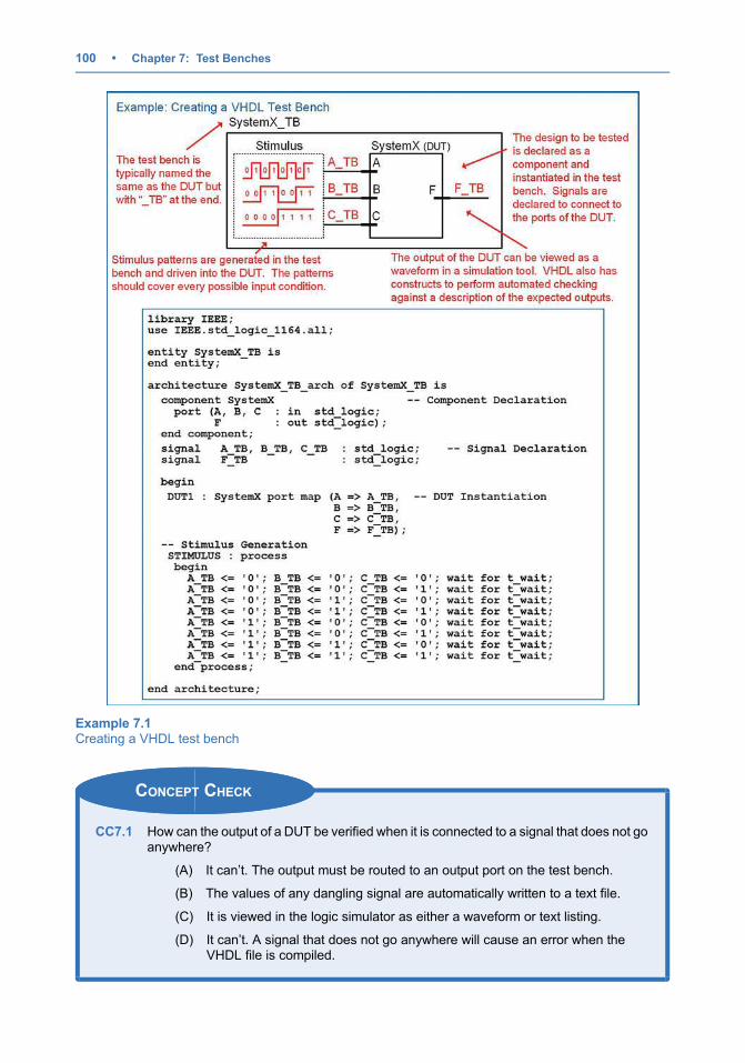
CONCEPT CHECK
CC7.1 How can the output of a DUT be verified when it is connected to a signal that does not goanywhere?
(A) It can’t. The output must be routed to an output port on the test bench.
(B) The values of any dangling signal are automatically written to a text file.
(C) It is viewed in the logic simulator as either a waveform or text listing.
(D) It can’t. A signal that does not go anywhere will cause an error when theVHDL file is compiled.
Example 7.1Creating a VHDL test bench
100 • Chapter 7: Test Benches
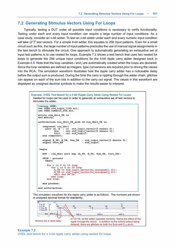
7.2 Generating Stimulus Vectors Using For Loops
Typically, testing a DUT under all possible input conditions is necessary to verify functionality.
Testing under each and every input condition can require a large number of input conditions. As a
case study, consider an n-bit adder. To test an n-bit adder under each and every numeric input condition
will take (2n)2 test vectors. For a simple 4-bit adder, this equates to 256 input patterns. Even for a small
circuit such as this, the large number of input patterns precludes the use of manual signal assignments in
the test bench to stimulate the circuit. One approach to automatically generating an exhaustive set of
input test patterns is to use nested for loops. Example 7.2 shows a test bench that uses two nested for
loops to generate the 256 unique input conditions for the 4-bit ripple carry adder designed back in
Example 4.8. Note that the loop variables i and j are automatically created when the loops are declared.
Since the loop variables are defined as integers, type conversions are required prior to driving the values
into the RCA. The simulation waveform illustrates how the ripple carry adder has a noticeable delay
before the output sum is produced. During the time the carry is rippling through the adder chain, glitches
can appear on each of the sum bits in addition to the carry out signal. The values in this waveform are
displayed as unsigned decimal symbols to make the results easier to interpret.
Example 7.2VHDL test bench for a 4-bit ripple carry adder using nested for loops
7.2 Generating Stimulus Vectors Using For Loops • 101

CONCEPT CHECK
CC7.2 If you used two nested for loops to generate an exhaustive set of patterns for the inputsof an 8-bit adder, how many patterns would be generated? There is no carry-in bit.
(A) 16
(B) 256
(C) 512
(D) 65,536
7.3 Automated Checking Using Report and Assert Statements
7.3.1 Report Statement
The keyword report can be used within a test bench in order to provide the status of the current test.
A report statement will print a string to the transcript window of the simulation tool. The report output also
contains an optional severity level. There are four levels of severity (ERROR, WARNING, NOTE, and
FAILURE). The severity level FAILURE will halt a simulation, while the levels ERROR, WARNING, and
NOTE will allow the simulation to continue. If the severity level is omitted, the report is assumed to be a
severity level of NOTE. The syntax for using a report statement is as follows:
report "string to be printed" severity <level>;
Let’s look at how we could use the report function within the example test bench to print the current
value of the input pattern to the transcript window of the simulator. Example 7.3 shows the new process
and resulting transcript output of the simulator when using report statements.
102 • Chapter 7: Test Benches
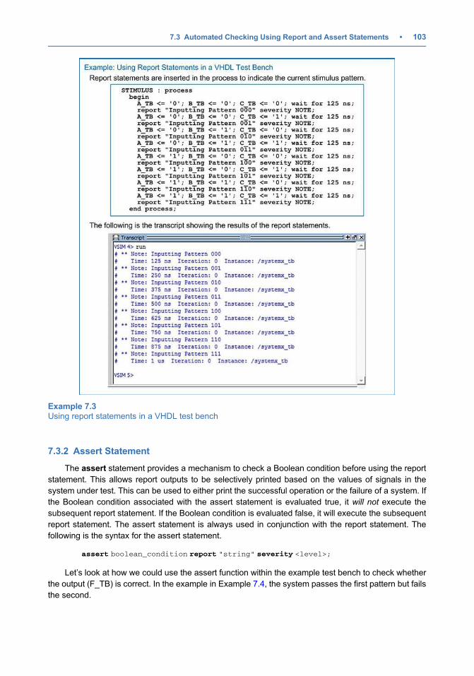
7.3.2 Assert Statement
The assert statement provides a mechanism to check a Boolean condition before using the report
statement. This allows report outputs to be selectively printed based on the values of signals in the
system under test. This can be used to either print the successful operation or the failure of a system. If
the Boolean condition associated with the assert statement is evaluated true, it will not execute the
subsequent report statement. If the Boolean condition is evaluated false, it will execute the subsequent
report statement. The assert statement is always used in conjunction with the report statement. The
following is the syntax for the assert statement.
assert boolean_condition report "string" severity <level>;
Let’s look at how we could use the assert function within the example test bench to check whether
the output (F_TB) is correct. In the example in Example 7.4, the system passes the first pattern but fails
the second.
Example 7.3Using report statements in a VHDL test bench
7.3 Automated Checking Using Report and Assert Statements • 103
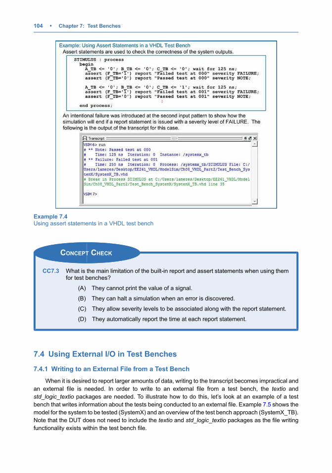
CONCEPT CHECK
CC7.3 What is the main limitation of the built-in report and assert statements when using themfor test benches?
(A) They cannot print the value of a signal.
(B) They can halt a simulation when an error is discovered.
(C) They allow severity levels to be associated along with the report statement.
(D) They automatically report the time at each report statement.
7.4 Using External I/O in Test Benches
7.4.1 Writing to an External File from a Test Bench
When it is desired to report larger amounts of data, writing to the transcript becomes impractical and
an external file is needed. In order to write to an external file from a test bench, the textio and
std_logic_textio packages are needed. To illustrate how to do this, let’s look at an example of a test
bench that writes information about the tests being conducted to an external file. Example 7.5 shows the
model for the system to be tested (SystemX) and an overview of the test bench approach (SystemX_TB).
Note that the DUT does not need to include the textio and std_logic_textio packages as the file writing
functionality exists within the test bench file.
Example 7.4Using assert statements in a VHDL test bench
104 • Chapter 7: Test Benches
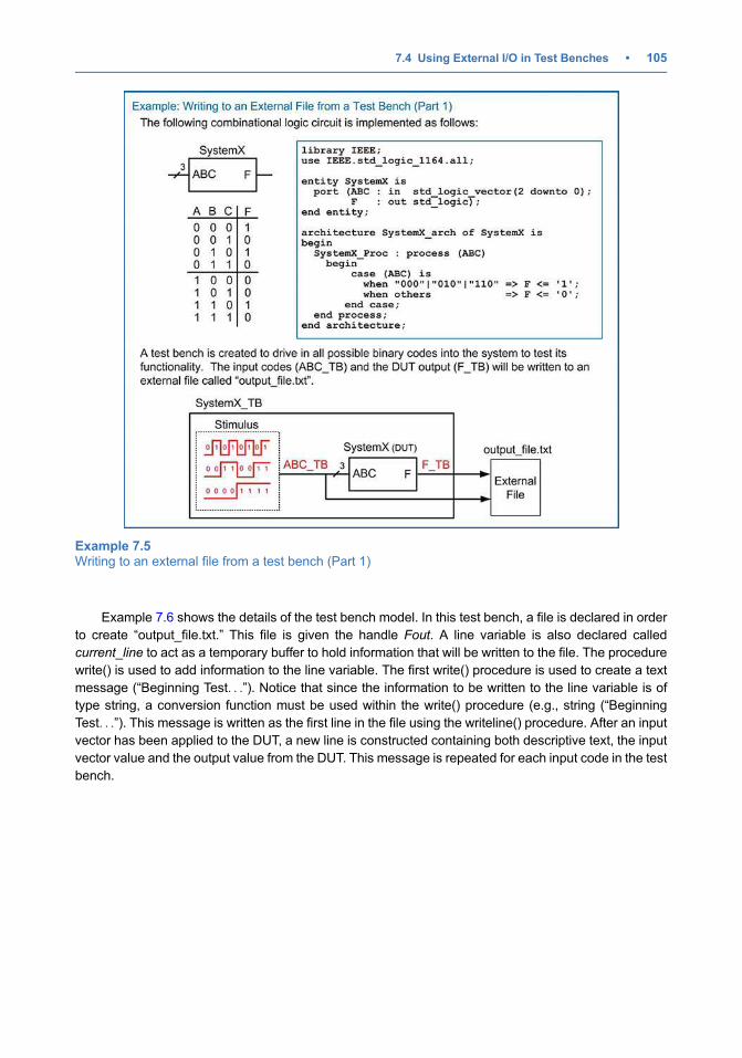
Example 7.6 shows the details of the test bench model. In this test bench, a file is declared in order
to create “output_file.txt.” This file is given the handle Fout. A line variable is also declared called
current_line to act as a temporary buffer to hold information that will be written to the file. The procedure
write() is used to add information to the line variable. The first write() procedure is used to create a text
message (“Beginning Test. . .”). Notice that since the information to be written to the line variable is of
type string, a conversion function must be used within the write() procedure (e.g., string (“Beginning
Test. . .”). This message is written as the first line in the file using the writeline() procedure. After an input
vector has been applied to the DUT, a new line is constructed containing both descriptive text, the input
vector value and the output value from the DUT. This message is repeated for each input code in the test
bench.
Example 7.5Writing to an external file from a test bench (Part 1)
7.4 Using External I/O in Test Benches • 105
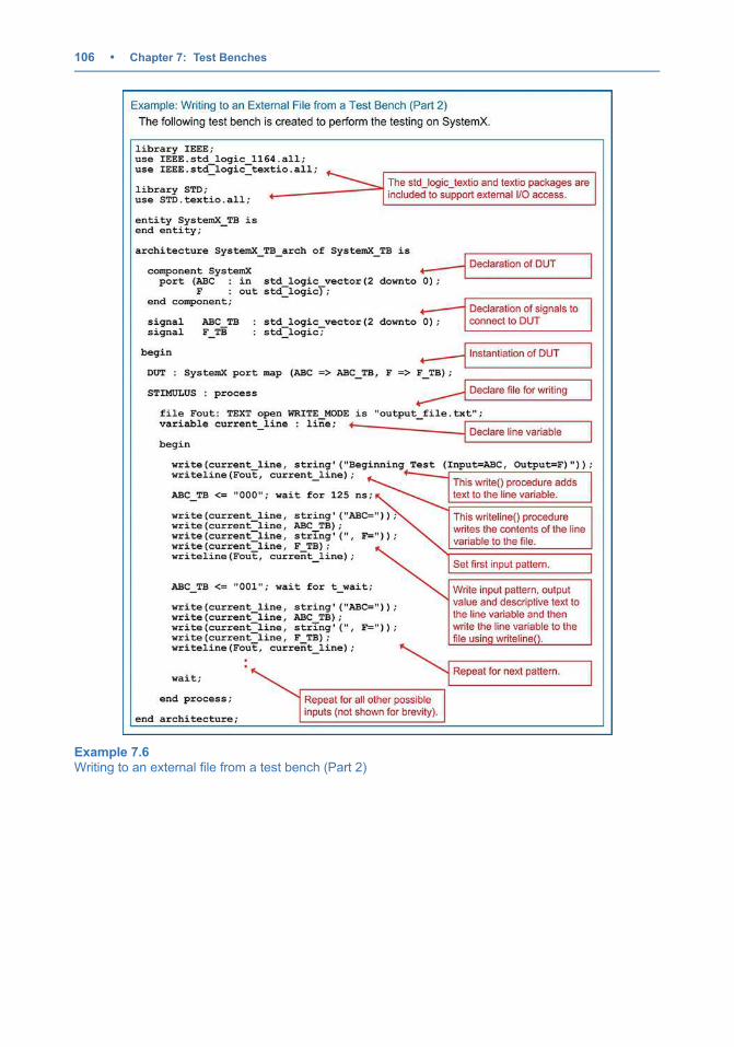
Example 7.6Writing to an external file from a test bench (Part 2)
106 • Chapter 7: Test Benches
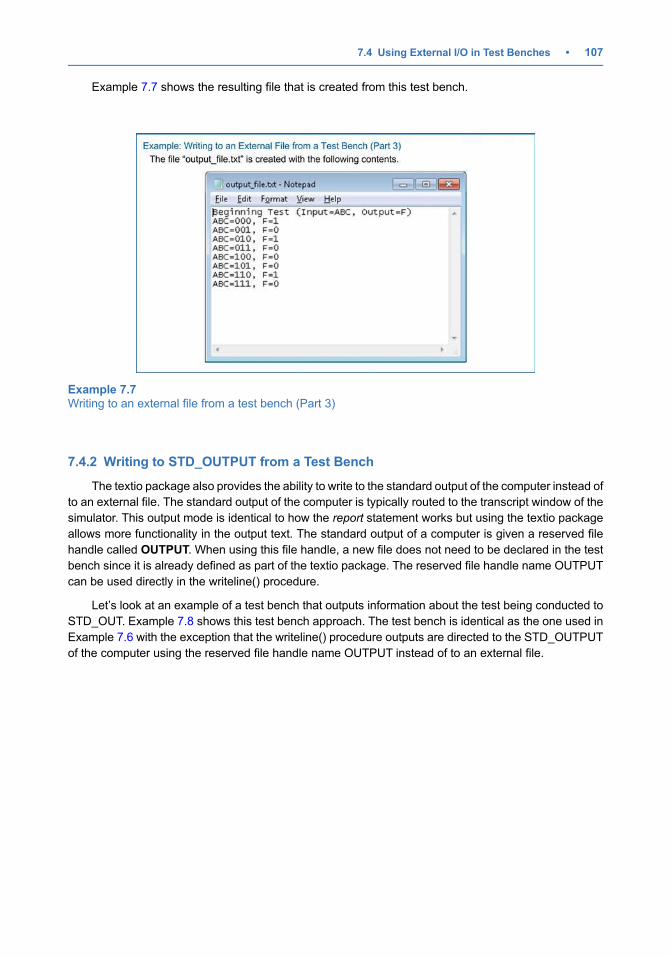
Example 7.7 shows the resulting file that is created from this test bench.
7.4.2 Writing to STD_OUTPUT from a Test Bench
The textio package also provides the ability to write to the standard output of the computer instead of
to an external file. The standard output of the computer is typically routed to the transcript window of the
simulator. This output mode is identical to how the report statement works but using the textio package
allows more functionality in the output text. The standard output of a computer is given a reserved file
handle called OUTPUT. When using this file handle, a new file does not need to be declared in the test
bench since it is already defined as part of the textio package. The reserved file handle name OUTPUT
can be used directly in the writeline() procedure.
Let’s look at an example of a test bench that outputs information about the test being conducted to
STD_OUT. Example 7.8 shows this test bench approach. The test bench is identical as the one used in
Example 7.6 with the exception that the writeline() procedure outputs are directed to the STD_OUTPUT
of the computer using the reserved file handle name OUTPUT instead of to an external file.
Example 7.7Writing to an external file from a test bench (Part 3)
7.4 Using External I/O in Test Benches • 107
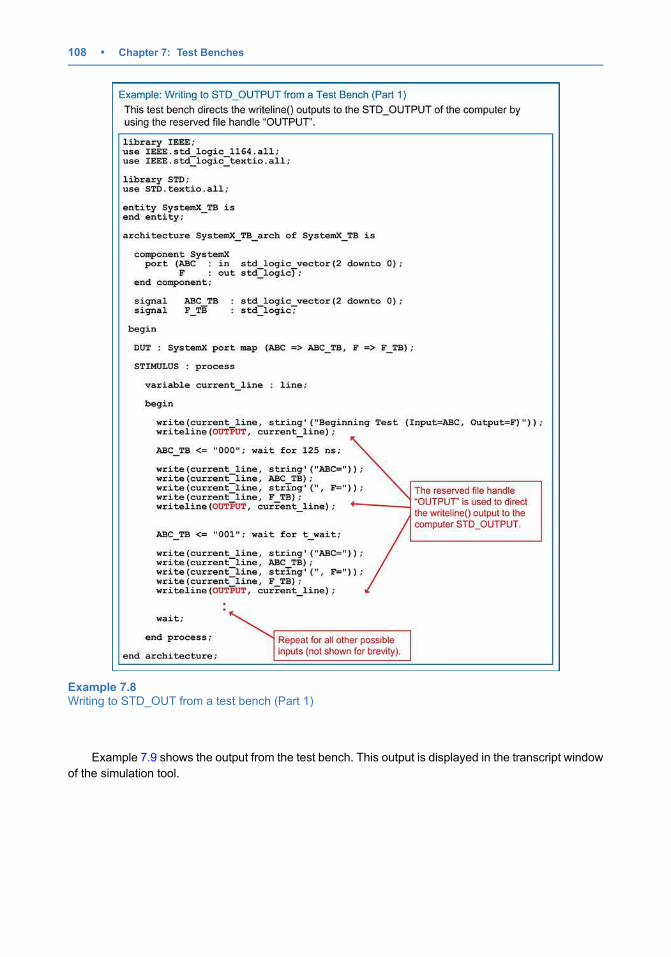
Example 7.9 shows the output from the test bench. This output is displayed in the transcript window
of the simulation tool.
Example 7.8Writing to STD_OUT from a test bench (Part 1)
108 • Chapter 7: Test Benches
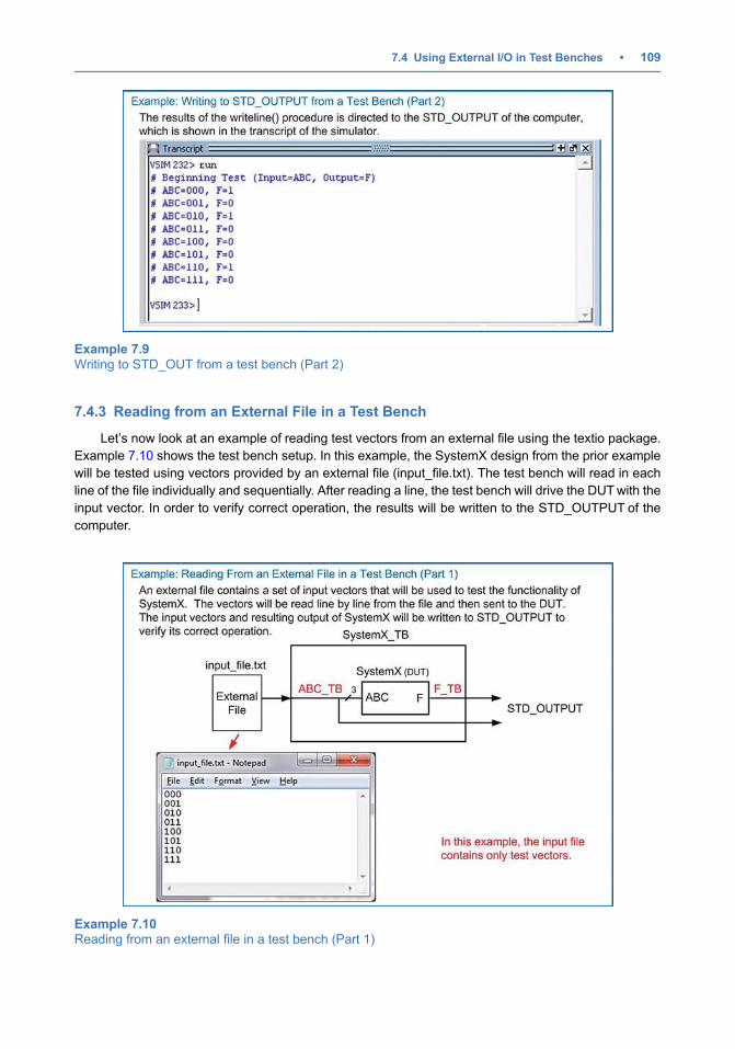
7.4.3 Reading from an External File in a Test Bench
Let’s now look at an example of reading test vectors from an external file using the textio package.
Example 7.10 shows the test bench setup. In this example, the SystemX design from the prior example
will be tested using vectors provided by an external file (input_file.txt). The test bench will read in each
line of the file individually and sequentially. After reading a line, the test bench will drive the DUTwith the
input vector. In order to verify correct operation, the results will be written to the STD_OUTPUT of the
computer.
Example 7.9Writing to STD_OUT from a test bench (Part 2)
Example 7.10Reading from an external file in a test bench (Part 1)
7.4 Using External I/O in Test Benches • 109
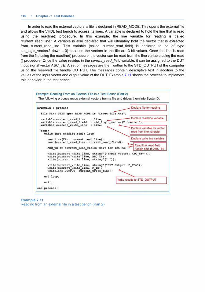
In order to read the external vectors, a file is declared in READ_MODE. This opens the external file
and allows the VHDL test bench to access its lines. A variable is declared to hold the line that is read
using the readline() procedure. In this example, the line variable for reading is called
“current_read_line.” A variable is also declared that will ultimately hold the vector that is extracted
from current_read_line. This variable (called current_read_field) is declared to be of type
std_logic_vector(2 downto 0) because the vectors in the file are 3-bit values. Once the line is read
from the file using the readline() procedure, the vector can be read from the line variable using the read
() procedure. Once the value resides in the current_read_field variable, it can be assigned to the DUT
input signal vector ABC_TB. A set of messages are then written to the STD_OUTPUTof the computer
using the reserved file handle OUTPUT. The messages contain descriptive text in addition to the
values of the input vector and output value of the DUT. Example 7.11 shows the process to implement
this behavior in the test bench.
Example 7.11Reading from an external file in a test bench (Part 2)
110 • Chapter 7: Test Benches
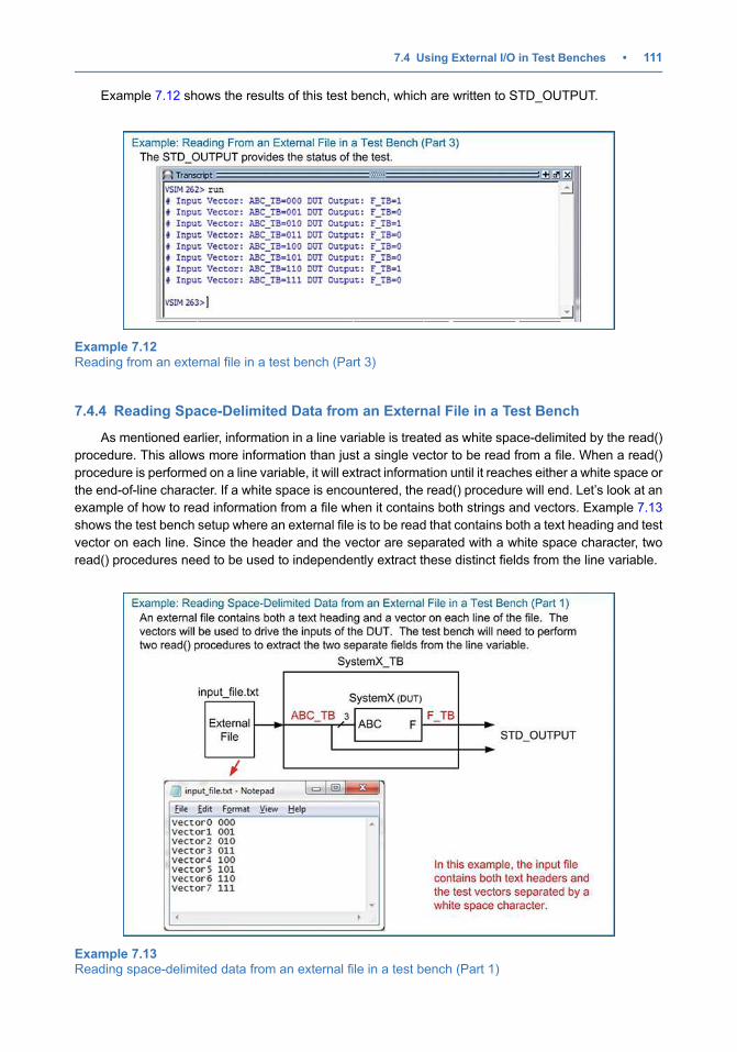
Example 7.12 shows the results of this test bench, which are written to STD_OUTPUT.
7.4.4 Reading Space-Delimited Data from an External File in a Test Bench
As mentioned earlier, information in a line variable is treated as white space-delimited by the read()
procedure. This allows more information than just a single vector to be read from a file. When a read()
procedure is performed on a line variable, it will extract information until it reaches either a white space or
the end-of-line character. If a white space is encountered, the read() procedure will end. Let’s look at an
example of how to read information from a file when it contains both strings and vectors. Example 7.13
shows the test bench setup where an external file is to be read that contains both a text heading and test
vector on each line. Since the header and the vector are separated with a white space character, two
read() procedures need to be used to independently extract these distinct fields from the line variable.
Example 7.12Reading from an external file in a test bench (Part 3)
Example 7.13Reading space-delimited data from an external file in a test bench (Part 1)
7.4 Using External I/O in Test Benches • 111
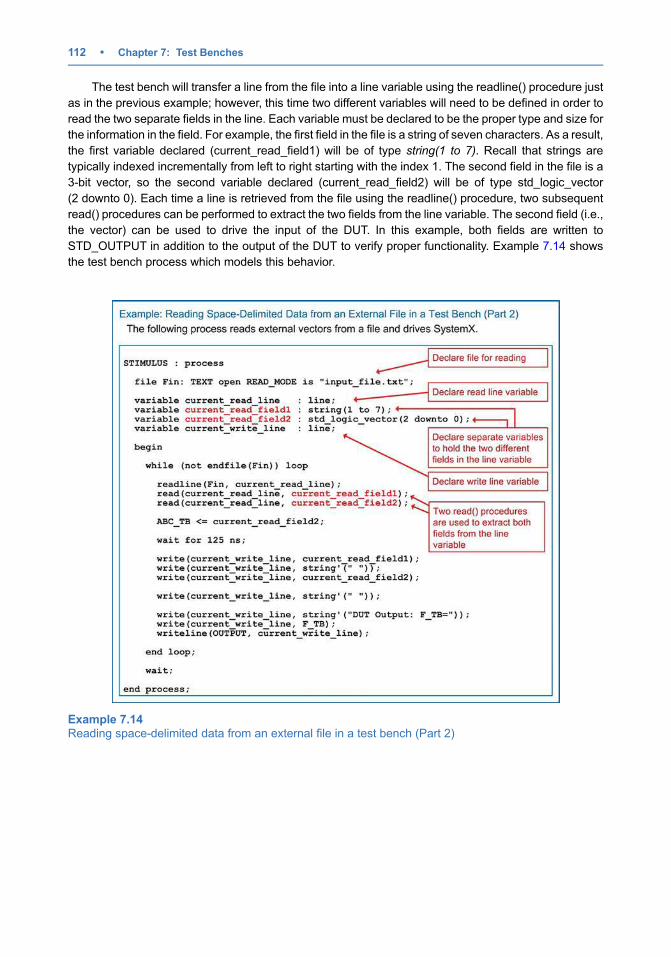
The test bench will transfer a line from the file into a line variable using the readline() procedure just
as in the previous example; however, this time two different variables will need to be defined in order to
read the two separate fields in the line. Each variable must be declared to be the proper type and size for
the information in the field. For example, the first field in the file is a string of seven characters. As a result,
the first variable declared (current_read_field1) will be of type string(1 to 7). Recall that strings are
typically indexed incrementally from left to right starting with the index 1. The second field in the file is a
3-bit vector, so the second variable declared (current_read_field2) will be of type std_logic_vector
(2 downto 0). Each time a line is retrieved from the file using the readline() procedure, two subsequent
read() procedures can be performed to extract the two fields from the line variable. The second field (i.e.,
the vector) can be used to drive the input of the DUT. In this example, both fields are written to
STD_OUTPUT in addition to the output of the DUT to verify proper functionality. Example 7.14 shows
the test bench process which models this behavior.
Example 7.14Reading space-delimited data from an external file in a test bench (Part 2)
112 • Chapter 7: Test Benches
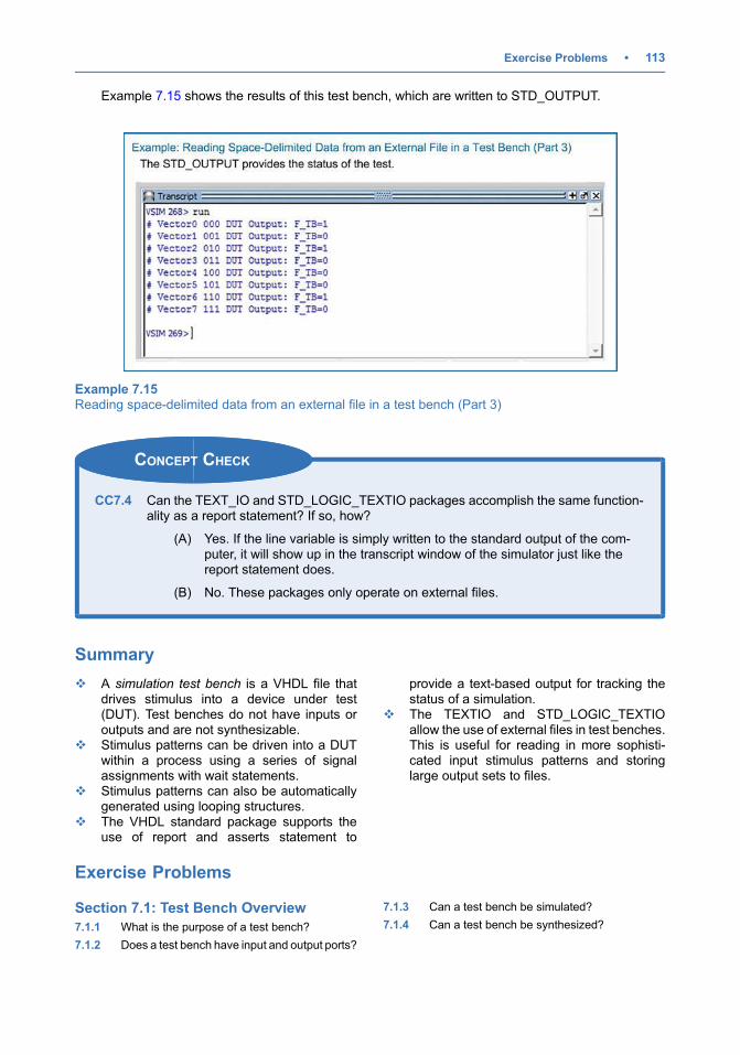
Example 7.15 shows the results of this test bench, which are written to STD_OUTPUT.
CONCEPT CHECK
CC7.4 Can the TEXT_IO and STD_LOGIC_TEXTIO packages accomplish the same function-ality as a report statement? If so, how?
(A) Yes. If the line variable is simply written to the standard output of the com-puter, it will show up in the transcript window of the simulator just like thereport statement does.
(B) No. These packages only operate on external files.
Summary
v A simulation test bench is a VHDL file thatdrives stimulus into a device under test(DUT). Test benches do not have inputs oroutputs and are not synthesizable.
v Stimulus patterns can be driven into a DUTwithin a process using a series of signalassignments with wait statements.
v Stimulus patterns can also be automaticallygenerated using looping structures.
v The VHDL standard package supports theuse of report and asserts statement to
provide a text-based output for tracking thestatus of a simulation.
v The TEXTIO and STD_LOGIC_TEXTIOallow the use of external files in test benches.This is useful for reading in more sophisti-cated input stimulus patterns and storinglarge output sets to files.
Exercise Problems
Section 7.1: Test Bench Overview
7.1.1 What is the purpose of a test bench?
7.1.2 Does a test bench have input and output ports?
7.1.3 Can a test bench be simulated?
7.1.4 Can a test bench be synthesized?
Example 7.15Reading space-delimited data from an external file in a test bench (Part 3)
Exercise Problems • 113
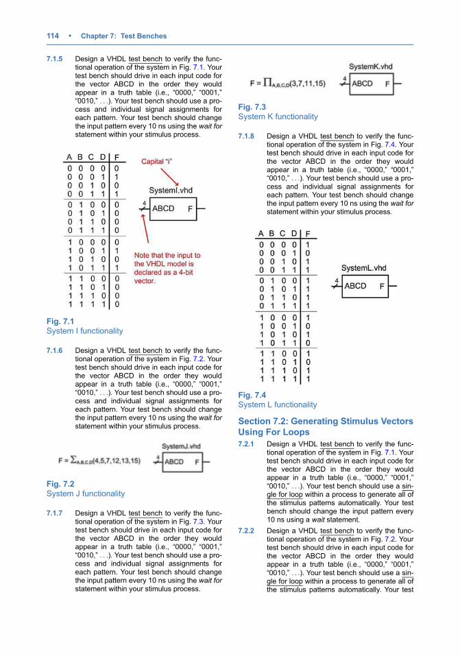
7.1.5 Design a VHDL test bench to verify the func-tional operation of the system in Fig. 7.1. Yourtest bench should drive in each input code forthe vector ABCD in the order they wouldappear in a truth table (i.e., “0000,” “0001,”“0010,” . . .). Your test bench should use a pro-cess and individual signal assignments foreach pattern. Your test bench should changethe input pattern every 10 ns using the wait forstatement within your stimulus process.
Fig. 7.1System I functionality
7.1.6 Design a VHDL test bench to verify the func-tional operation of the system in Fig. 7.2. Yourtest bench should drive in each input code forthe vector ABCD in the order they wouldappear in a truth table (i.e., “0000,” “0001,”“0010,” . . .). Your test bench should use a pro-cess and individual signal assignments foreach pattern. Your test bench should changethe input pattern every 10 ns using the wait forstatement within your stimulus process.
Fig. 7.2System J functionality
7.1.7 Design a VHDL test bench to verify the func-tional operation of the system in Fig. 7.3. Yourtest bench should drive in each input code forthe vector ABCD in the order they wouldappear in a truth table (i.e., “0000,” “0001,”“0010,” . . .). Your test bench should use a pro-cess and individual signal assignments foreach pattern. Your test bench should changethe input pattern every 10 ns using the wait forstatement within your stimulus process.
Fig. 7.3System K functionality
7.1.8 Design a VHDL test bench to verify the func-tional operation of the system in Fig. 7.4. Yourtest bench should drive in each input code forthe vector ABCD in the order they wouldappear in a truth table (i.e., “0000,” “0001,”“0010,” . . .). Your test bench should use a pro-cess and individual signal assignments foreach pattern. Your test bench should changethe input pattern every 10 ns using the wait forstatement within your stimulus process.
Fig. 7.4System L functionality
Section 7.2: Generating Stimulus Vectors
Using For Loops
7.2.1 Design a VHDL test bench to verify the func-tional operation of the system in Fig. 7.1. Yourtest bench should drive in each input code forthe vector ABCD in the order they wouldappear in a truth table (i.e., “0000,” “0001,”“0010,” . . .). Your test bench should use a sin-gle for loop within a process to generate all ofthe stimulus patterns automatically. Your testbench should change the input pattern every10 ns using a wait statement.
7.2.2 Design a VHDL test bench to verify the func-tional operation of the system in Fig. 7.2. Yourtest bench should drive in each input code forthe vector ABCD in the order they wouldappear in a truth table (i.e., “0000,” “0001,”“0010,” . . .). Your test bench should use a sin-gle for loop within a process to generate all ofthe stimulus patterns automatically. Your test
114 • Chapter 7: Test Benches
bench should change the input pattern every10 ns using a wait statement.
7.2.3 Design a VHDL test bench to verify the func-tional operation of the system in Fig. 7.3. Yourtest bench should drive in each input code forthe vector ABCD in the order they wouldappear in a truth table (i.e., “0000,” “0001,”“0010,” . . .). Your test bench should use a sin-gle for loop within a process to generate all ofthe stimulus patterns automatically. Your testbench should change the input pattern every10 ns using a wait statement.
7.2.4 Design a VHDL test bench to verify the func-tional operation of the system in Fig. 7.4. Yourtest bench should drive in each input code forthe vector ABCD in the order they wouldappear in a truth table (i.e., “0000,” “0001,”“0010,” . . .). Your test bench should use a sin-gle for loop within a process to generate all ofthe stimulus patterns automatically. Your testbench should change the input pattern every10 ns using a wait statement.
7.2.5 Design a VHDL model for an 8-bit Ripple CarryAdder (RCA) using a structural designapproach. This involves creating a half adder(half_adder.vhd), full adder (full_adder.vhd),and then finally a top level adder (rca.vhd) byinstantiating eight full adder components.Model the ripple delay by inserting 1 ns ofgate delay for the XOR, AND, and ORoperators using a delayed signal assignment.The general topology and entity definition forthe design are shown in Example 4.6. Design aVHDL test bench to exhaustively verify thisdesign under all input conditions. Your testbench should use two nested for loops withina process to generate all of the stimuluspatterns automatically. Your test bench shouldchange the input pattern every 30 ns using await statement in order to give sufficient timefor the signals to ripple through the adder.
Section 7.3: Automated Checking Using
Report and Assert Statements
7.3.1 Design a VHDL test bench to verify the func-tional operation of the system in Fig. 7.1. Yourtest bench should drive in each input code forthe vector ABCD in the order they wouldappear in a truth table (i.e., “0000,” “0001,”“0010,” . . .). Your test bench should changethe input pattern every 10 ns using a waitstatement. Use the report and assertstatements to output a message on the statusof each test to the simulation transcript window.For each input vector, create a message thatindicates the current input vector being tested,the resulting output of your DUT, and whetherthe DUToutput is correct.
7.3.2 Design a VHDL test bench to verify the func-tional operation of the system in Fig. 7.2. Yourtest bench should drive in each input code forthe vector ABCD in the order they would
appear in a truth table (i.e., “0000,” “0001,”“0010,” . . .). Your test bench should changethe input pattern every 10 ns using a waitstatement. Use the report and assertstatements to output a message on the statusof each test to the simulation transcript window.For each input vector, create a message thatindicates the current input vector being tested,the resulting output of your DUT, and whetherthe DUToutput is correct.
7.3.3 Design a VHDL test bench to verify the func-tional operation of the system in Fig. 7.3. Yourtest bench should drive in each input code forthe vector ABCD in the order they wouldappear in a truth table (i.e., “0000,” “0001,”“0010,” . . .). Your test bench should changethe input pattern every 10 ns using a waitstatement. Use the report and assertstatements to output a message on the statusof each test to the simulation transcript window.For each input vector, create a message thatindicates the current input vector being tested,the resulting output of your DUT, and whetherthe DUToutput is correct.
7.3.4 Design a VHDL test bench to verify the func-tional operation of the system in Fig. 7.4. Yourtest bench should drive in each input code forthe vector ABCD in the order they wouldappear in a truth table (i.e., “0000,” “0001,”“0010,” . . .). Your test bench should changethe input pattern every 10 ns using a waitstatement. Use the report and assertstatements to output a message on the statusof each test to the simulation transcript window.For each input vector, create a message thatindicates the current input vector being tested,the resulting output of your DUT, and whetherthe DUToutput is correct.
Section 7.4: Using External I/O in Test
Benches
7.4.1 Design a VHDL test bench to verify the func-tional operation of the system in Fig. 7.1. Yourtest bench should drive in each input code forthe vector ABCD in the order they wouldappear in a truth table (i.e., “0000,” “0001,”“0010,” . . .). Your test bench should use a pro-cess and individual signal assignments foreach pattern. Your test bench should changethe input pattern every 10 ns using the wait forstatement within your stimulus process. Writethe output results to an external file called“output_vectors.txt” using the TEXTIO andSTD_LOGIC_TEXTIO packages.
7.4.2 Design a VHDL test bench to verify the func-tional operation of the system in Fig. 7.2. Yourtest bench should drive in each input code forthe vector ABCD in the order they wouldappear in a truth table (i.e., “0000,” “0001,”“0010,” . . .). Your test bench should use a pro-cess and individual signal assignments foreach pattern. Your test bench should change
Exercise Problems • 115
the input pattern every 10 ns using the wait forstatement within your stimulus process. Writethe output results to the STD_OUTPUT of thesimulator using the TEXTIO andSTD_LOGIC_TEXTIO packages.
7.4.3 Design a VHDL test bench to verify the func-tional operation of the system in Fig. 7.3. Cre-ate an input text file called “input_vectors.txt”that contains each input code for the vectorABCD in the order they would appear in atruth table (i.e., “0000,” “0001,” “0010,” . . .) ona separate line. Use the TEXTIO andSTD_LOGIC_TEXTIO packages to read ineach line of the file individually and use thecorresponding input vector to drive the DUT.
Write the output results to an external filecalled “output_vectors.txt.”
7.4.4 Design a VHDL test bench to verify the func-tional operation of the system in Fig. 7.4. Cre-ate an input text file called “input_vectors.txt”that contains each input code for the vectorABCD in the order they would appear in atruth table (i.e., “0000,” “0001,” “0010,” . . .) ona separate line. Use the TEXTIO andSTD_LOGIC_TEXTIO packages to read ineach line of the file individually and use thecorresponding input vector to drive the DUT.Write the output results to the STD_OUTPUTof the simulator.
116 • Chapter 7: Test Benches
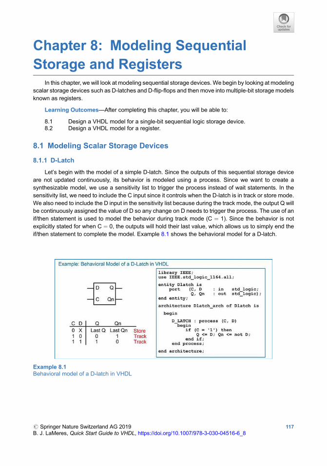
Chapter 8: Modeling Sequential
Storage and RegistersIn this chapter, we will look at modeling sequential storage devices. We begin by looking at modeling
scalar storage devices such as D-latches and D-flip-flops and then move into multiple-bit storage models
known as registers.
Learning Outcomes—After completing this chapter, you will be able to:
8.1 Design a VHDL model for a single-bit sequential logic storage device.8.2 Design a VHDL model for a register.
8.1 Modeling Scalar Storage Devices
8.1.1 D-Latch
Let’s begin with the model of a simple D-latch. Since the outputs of this sequential storage device
are not updated continuously, its behavior is modeled using a process. Since we want to create a
synthesizable model, we use a sensitivity list to trigger the process instead of wait statements. In the
sensitivity list, we need to include the C input since it controls when the D-latch is in track or store mode.
We also need to include the D input in the sensitivity list because during the track mode, the output Q will
be continuously assigned the value of D so any change on D needs to trigger the process. The use of an
if/then statement is used to model the behavior during track mode (C ¼ 1). Since the behavior is not
explicitly stated for when C ¼ 0, the outputs will hold their last value, which allows us to simply end the
if/then statement to complete the model. Example 8.1 shows the behavioral model for a D-latch.
Example 8.1Behavioral model of a D-latch in VHDL
# Springer Nature Switzerland AG 2019
B. J. LaMeres, Quick Start Guide to VHDL, https://doi.org/10.1007/978-3-030-04516-6_8
117
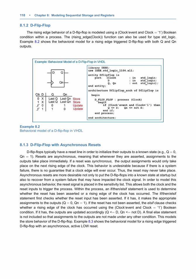
8.1.2 D-Flip-Flop
The rising edge behavior of a D-flip-flop is modeled using a (Clock‘event and Clock ¼ ‘1’) Boolean
condition within a process. The (rising_edge(Clock)) function can also be used for type std_logic.
Example 8.2 shows the behavioral model for a rising edge triggered D-flip-flop with both Q and Qn
outputs.
8.1.3 D-Flip-Flop with Asynchronous Resets
D-flip-flops typically have a reset line in order to initialize their outputs to a known state (e.g., Q ¼ 0,
Qn ¼ 1). Resets are asynchronous, meaning that whenever they are asserted, assignments to the
outputs take place immediately. If a reset was synchronous, the output assignments would only take
place on the next rising edge of the clock. This behavior is undesirable because if there is a system
failure, there is no guarantee that a clock edge will ever occur. Thus, the reset may never take place.
Asynchronous resets are more desirable not only to put the D-flip-flops into a known state at startup but
also to recover from a system failure that may have impacted the clock signal. In order to model this
asynchronous behavior, the reset signal is placed in the sensitivity list. This allows both the clock and the
reset inputs to trigger the process. Within the process, an if/then/elsif statement is used to determine
whether the reset has been asserted or a rising edge of the clock has occurred. The if/then/elsif
statement first checks whether the reset input has been asserted. If it has, it makes the appropriate
assignments to the outputs (Q ¼ 0, Qn ¼ 1). If the reset has not been asserted, the elsif clause checks
whether a rising edge of the clock has occurred using the (Clock‘event and Clock ¼ ‘1’) Boolean
condition. If it has, the outputs are updated accordingly (Q <¼ D, Qn <¼ not D). A final else statement
is not included so that assignments to the outputs are not made under any other condition. This models
the store behavior of the D-flip-flop. Example 8.3 shows the behavioral model for a rising edge triggered
D-flip-flop with an asynchronous, active LOW reset.
Example 8.2Behavioral model of a D-flip-flop in VHDL
118 • Chapter 8: Modeling Sequential Storage and Registers
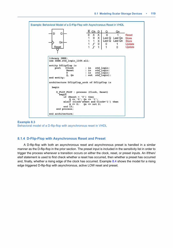
8.1.4 D-Flip-Flop with Asynchronous Reset and Preset
A D-flip-flop with both an asynchronous reset and asynchronous preset is handled in a similar
manner as the D-flip-flop in the prior section. The preset input is included in the sensitivity list in order to
trigger the process whenever a transition occurs on either the clock, reset, or preset inputs. An if/then/
elsif statement is used to first check whether a reset has occurred, then whether a preset has occurred
and, finally, whether a rising edge of the clock has occurred. Example 8.4 shows the model for a rising
edge triggered D-flip-flop with asynchronous, active LOW reset and preset.
Example 8.3Behavioral model of a D-flip-flop with asynchronous reset in VHDL
8.1 Modeling Scalar Storage Devices • 119
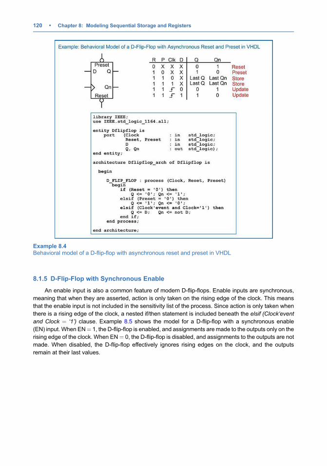
8.1.5 D-Flip-Flop with Synchronous Enable
An enable input is also a common feature of modern D-flip-flops. Enable inputs are synchronous,
meaning that when they are asserted, action is only taken on the rising edge of the clock. This means
that the enable input is not included in the sensitivity list of the process. Since action is only taken when
there is a rising edge of the clock, a nested if/then statement is included beneath the elsif (Clock‘event
and Clock ¼ ‘1’) clause. Example 8.5 shows the model for a D-flip-flop with a synchronous enable
(EN) input. When EN¼ 1, the D-flip-flop is enabled, and assignments are made to the outputs only on the
rising edge of the clock. When EN¼ 0, the D-flip-flop is disabled, and assignments to the outputs are not
made. When disabled, the D-flip-flop effectively ignores rising edges on the clock, and the outputs
remain at their last values.
Example 8.4Behavioral model of a D-flip-flop with asynchronous reset and preset in VHDL
120 • Chapter 8: Modeling Sequential Storage and Registers
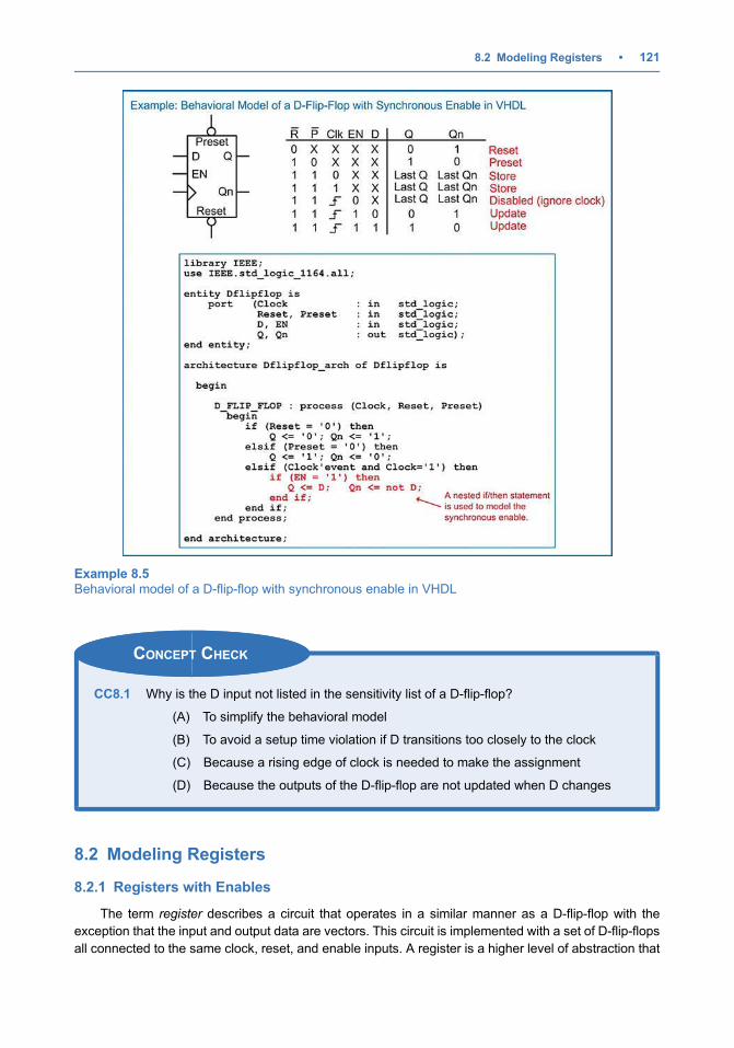
CONCEPT CHECK
CC8.1 Why is the D input not listed in the sensitivity list of a D-flip-flop?
(A) To simplify the behavioral model
(B) To avoid a setup time violation if D transitions too closely to the clock
(C) Because a rising edge of clock is needed to make the assignment
(D) Because the outputs of the D-flip-flop are not updated when D changes
8.2 Modeling Registers
8.2.1 Registers with Enables
The term register describes a circuit that operates in a similar manner as a D-flip-flop with the
exception that the input and output data are vectors. This circuit is implemented with a set of D-flip-flops
all connected to the same clock, reset, and enable inputs. A register is a higher level of abstraction that
Example 8.5Behavioral model of a D-flip-flop with synchronous enable in VHDL
8.2 Modeling Registers • 121
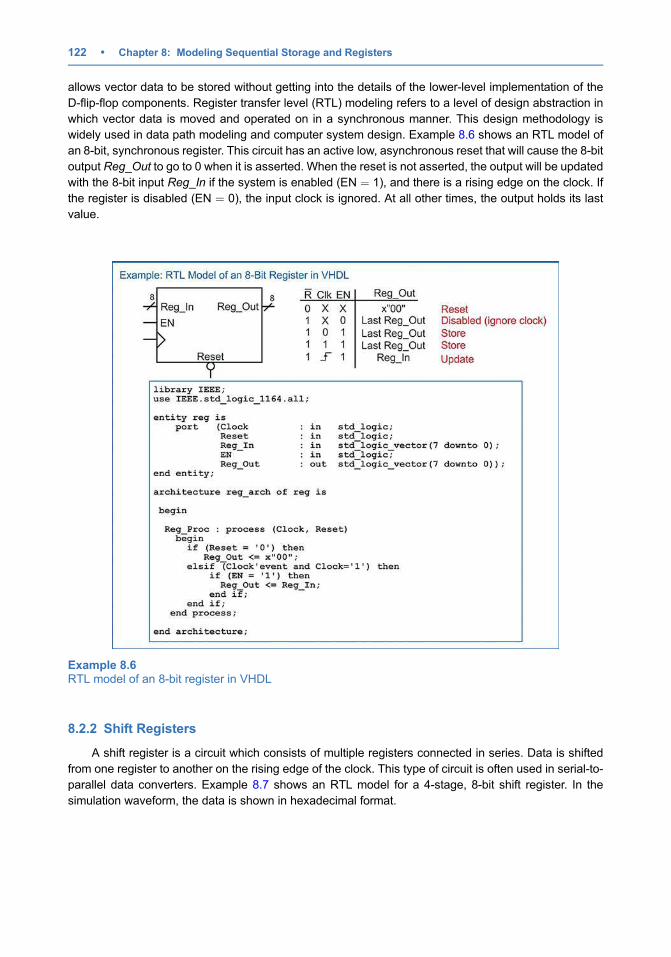
allows vector data to be stored without getting into the details of the lower-level implementation of the
D-flip-flop components. Register transfer level (RTL) modeling refers to a level of design abstraction in
which vector data is moved and operated on in a synchronous manner. This design methodology is
widely used in data path modeling and computer system design. Example 8.6 shows an RTL model of
an 8-bit, synchronous register. This circuit has an active low, asynchronous reset that will cause the 8-bit
output Reg_Out to go to 0 when it is asserted. When the reset is not asserted, the output will be updated
with the 8-bit input Reg_In if the system is enabled (EN ¼ 1), and there is a rising edge on the clock. If
the register is disabled (EN ¼ 0), the input clock is ignored. At all other times, the output holds its last
value.
8.2.2 Shift Registers
A shift register is a circuit which consists of multiple registers connected in series. Data is shifted
from one register to another on the rising edge of the clock. This type of circuit is often used in serial-to-
parallel data converters. Example 8.7 shows an RTL model for a 4-stage, 8-bit shift register. In the
simulation waveform, the data is shown in hexadecimal format.
Example 8.6RTL model of an 8-bit register in VHDL
122 • Chapter 8: Modeling Sequential Storage and Registers
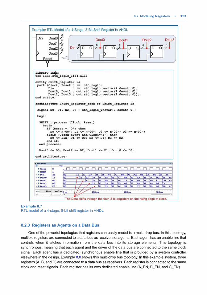
8.2.3 Registers as Agents on a Data Bus
One of the powerful topologies that registers can easily model is a multi-drop bus. In this topology,
multiple registers are connected to a data bus as receivers or agents. Each agent has an enable line that
controls when it latches information from the data bus into its storage elements. This topology is
synchronous, meaning that each agent and the driver of the data bus are connected to the same clock
signal. Each agent has a dedicated, synchronous enable line that is provided by a system controller
elsewhere in the design. Example 8.8 shows this multi-drop bus topology. In this example system, three
registers (A, B, and C) are connected to a data bus as receivers. Each register is connected to the same
clock and reset signals. Each register has its own dedicated enable line (A_EN, B_EN, and C_EN).
Example 8.7RTL model of a 4-stage, 8-bit shift register in VHDL
8.2 Modeling Registers • 123
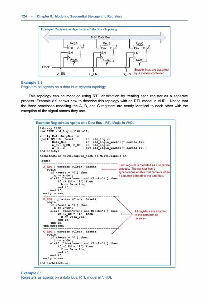
This topology can be modeled using RTL abstraction by treating each register as a separate
process. Example 8.9 shows how to describe this topology with an RTL model in VHDL. Notice that
the three processes modeling the A, B, and C registers are nearly identical to each other with the
exception of the signal names they use.
Example 8.8Registers as agents on a data bus: system topology
Example 8.9Registers as agents on a data bus: RTL model in VHDL
124 • Chapter 8: Modeling Sequential Storage and Registers
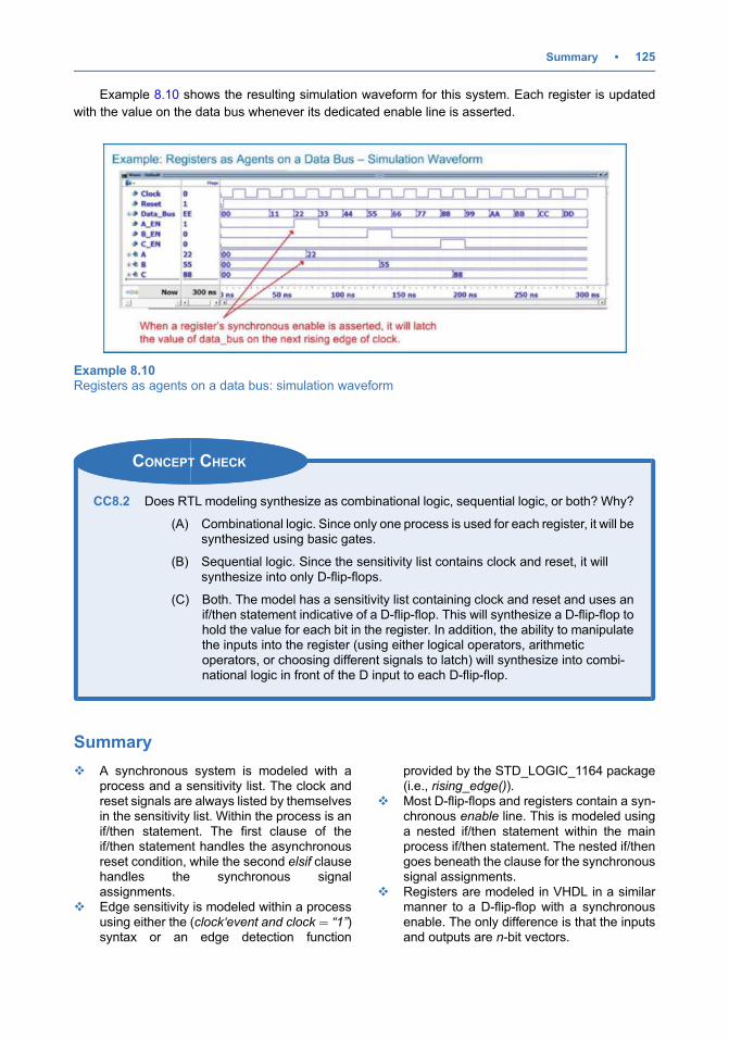
Example 8.10 shows the resulting simulation waveform for this system. Each register is updated
with the value on the data bus whenever its dedicated enable line is asserted.
CONCEPT CHECK
CC8.2 Does RTL modeling synthesize as combinational logic, sequential logic, or both? Why?
(A) Combinational logic. Since only one process is used for each register, it will besynthesized using basic gates.
(B) Sequential logic. Since the sensitivity list contains clock and reset, it willsynthesize into only D-flip-flops.
(C) Both. The model has a sensitivity list containing clock and reset and uses anif/then statement indicative of a D-flip-flop. This will synthesize a D-flip-flop tohold the value for each bit in the register. In addition, the ability to manipulatethe inputs into the register (using either logical operators, arithmeticoperators, or choosing different signals to latch) will synthesize into combi-national logic in front of the D input to each D-flip-flop.
Summary
v A synchronous system is modeled with aprocess and a sensitivity list. The clock andreset signals are always listed by themselvesin the sensitivity list. Within the process is anif/then statement. The first clause of theif/then statement handles the asynchronousreset condition, while the second elsif clausehandles the synchronous signalassignments.
v Edge sensitivity is modeled within a processusing either the (clock‘event and clock ¼ “1”)syntax or an edge detection function
provided by the STD_LOGIC_1164 package(i.e., rising_edge()).
v Most D-flip-flops and registers contain a syn-chronous enable line. This is modeled usinga nested if/then statement within the mainprocess if/then statement. The nested if/thengoes beneath the clause for the synchronoussignal assignments.
v Registers are modeled in VHDL in a similarmanner to a D-flip-flop with a synchronousenable. The only difference is that the inputsand outputs are n-bit vectors.
Example 8.10Registers as agents on a data bus: simulation waveform
Summary • 125
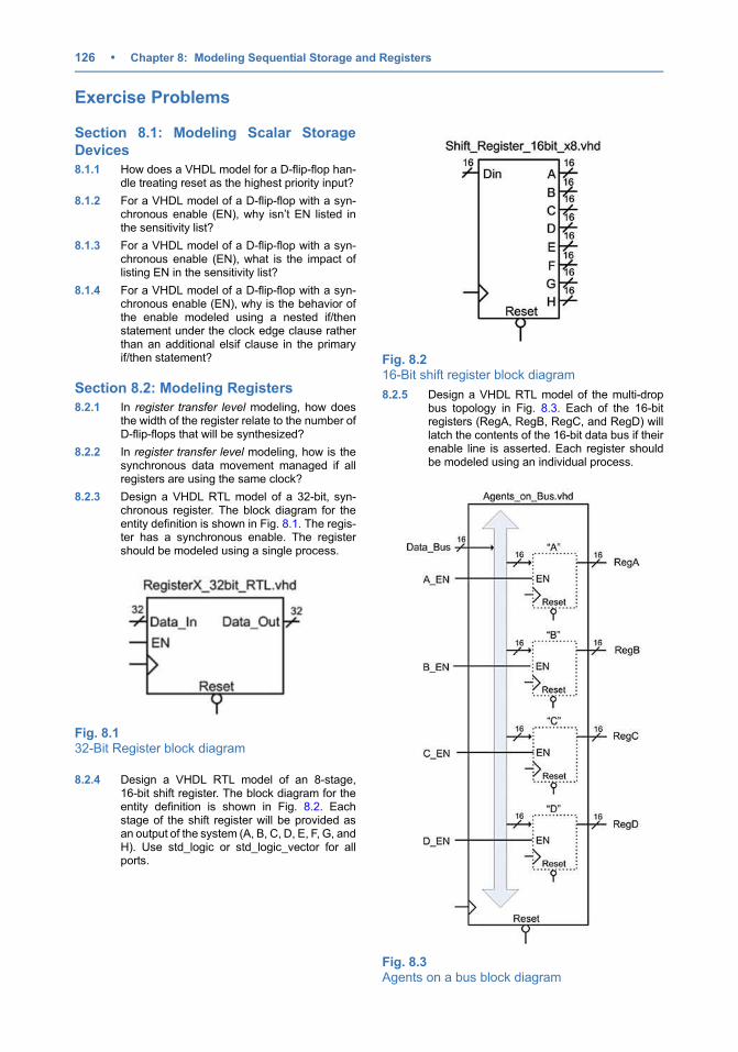
Exercise Problems
Section 8.1: Modeling Scalar Storage
Devices
8.1.1 How does a VHDL model for a D-flip-flop han-dle treating reset as the highest priority input?
8.1.2 For a VHDL model of a D-flip-flop with a syn-chronous enable (EN), why isn’t EN listed inthe sensitivity list?
8.1.3 For a VHDL model of a D-flip-flop with a syn-chronous enable (EN), what is the impact oflisting EN in the sensitivity list?
8.1.4 For a VHDL model of a D-flip-flop with a syn-chronous enable (EN), why is the behavior ofthe enable modeled using a nested if/thenstatement under the clock edge clause ratherthan an additional elsif clause in the primaryif/then statement?
Section 8.2: Modeling Registers
8.2.1 In register transfer level modeling, how doesthe width of the register relate to the number ofD-flip-flops that will be synthesized?
8.2.2 In register transfer level modeling, how is thesynchronous data movement managed if allregisters are using the same clock?
8.2.3 Design a VHDL RTL model of a 32-bit, syn-chronous register. The block diagram for theentity definition is shown in Fig. 8.1. The regis-ter has a synchronous enable. The registershould be modeled using a single process.
Fig. 8.132-Bit Register block diagram
8.2.4 Design a VHDL RTL model of an 8-stage,16-bit shift register. The block diagram for theentity definition is shown in Fig. 8.2. Eachstage of the shift register will be provided asan output of the system (A, B, C, D, E, F, G, andH). Use std_logic or std_logic_vector for allports.
Fig. 8.216-Bit shift register block diagram
8.2.5 Design a VHDL RTL model of the multi-dropbus topology in Fig. 8.3. Each of the 16-bitregisters (RegA, RegB, RegC, and RegD) willlatch the contents of the 16-bit data bus if theirenable line is asserted. Each register shouldbe modeled using an individual process.
Fig. 8.3Agents on a bus block diagram
126 • Chapter 8: Modeling Sequential Storage and Registers
Chapter 9: Modeling Finite State
MachinesIn this chapter, we will look at modeling finite state machines (FSMs). An FSM is one of the most
powerful circuits in a digital system because it can make decisions about the next output based on both
the current and past inputs. Finite state machines are modeled using the constructs already covered in
this book. In this chapter, we will look at the widely accepted three-process model for designing a FSM.
Learning Outcomes—After completing this chapter, you will be able to:
9.1 Describe the three-process modeling approach for FSM design.9.2 Design a VHDL model for a FSM from a state diagram.
9.1 The FSM Design Process and a Push-Button Window
Controller Example
The most common modeling practice for FSMs is to create a new user-defined type that can take
on the descriptive state names from the state diagram. Two signals are then created of this type,
current_state and next_state. Once these signals are created, all of the functional blocks in the state
machine can use the descriptive state names in their conditional signal assignments. The synthesizer
will automatically assign the state codes based on the most effective use of the target technology (e.g.,
binary, gray code, one-hot). Within the VHDL state machine model, three processes are used to describe
each of the functional blocks, state memory, next state logic, and output logic. In order to examine how to
model a finite state machine using this approach, let’s use a push-button window controller example.
Example 9.1 gives the overview of the design objectives for this example and the state diagram
describing the behavior to be modeled in VHDL.
# Springer Nature Switzerland AG 2019
B. J. LaMeres, Quick Start Guide to VHDL, https://doi.org/10.1007/978-3-030-04516-6_9
127
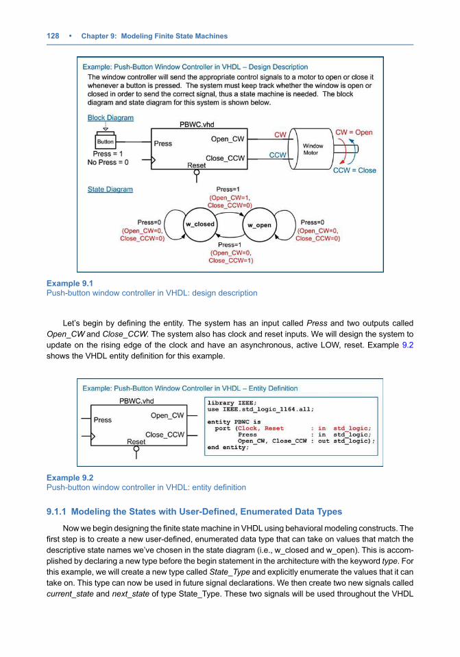
Let’s begin by defining the entity. The system has an input called Press and two outputs called
Open_CW and Close_CCW. The system also has clock and reset inputs. We will design the system to
update on the rising edge of the clock and have an asynchronous, active LOW, reset. Example 9.2
shows the VHDL entity definition for this example.
9.1.1 Modeling the States with User-Defined, Enumerated Data Types
Nowwe begin designing the finite state machine in VHDL using behavioral modeling constructs. The
first step is to create a new user-defined, enumerated data type that can take on values that match the
descriptive state names we’ve chosen in the state diagram (i.e., w_closed and w_open). This is accom-
plished by declaring a new type before the begin statement in the architecture with the keyword type. For
this example, we will create a new type called State_Type and explicitly enumerate the values that it can
take on. This type can now be used in future signal declarations. We then create two new signals called
current_state and next_state of type State_Type. These two signals will be used throughout the VHDL
Example 9.2Push-button window controller in VHDL: entity definition
Example 9.1Push-button window controller in VHDL: design description
128 • Chapter 9: Modeling Finite State Machines
model in order to provide a high-level, readable description of the FSM behavior. The following syntax
shows how to declare the new type and declare the current_state and next_state signals.
type State_Type is (w_closed, w_open);
signal current_state, next_state : State_Type;
9.1.2 The State Memory Process
Now we model the state memory of the FSM using a process. This process models the behavior of
the D-flip-flops in the FSM that are holding the current state on their Q outputs. Each time there is a rising
edge of the clock, the current state is updated with the next state value present on the D inputs of the
D-flip-flops. This process must also model the reset condition. For this example, we will have the state
machine go to the w_closed state when Reset is asserted. At all other times, the process will simply
update current_state with next_state on every rising edge of the clock. The process model is very similar
to the model of a D-flip-flop. This is as expected since this process will synthesize into one or more D-flip-
flops to hold the current state. The sensitivity list contains only Clock and Reset, and assignments are
only made to the signal current_state. The following syntax shows how to model the state memory of this
FSM example:
STATE_MEMORY : process (Clock, Reset)
begin
if (Reset ¼ ’0’) then
current_state <¼ w_closed;
elsif (Clock’event and Clock¼’1’) then
current_state <¼ next_state;
end if;
end process;
9.1.3 The Next State Logic Process
Now we model the next state logic of the FSM using a second process. Recall that the next state
logic is combinational logic, thus we need to include all of the input signals that the circuit considers in the
next state calculation in the sensitivity list. The current_state signal will always be included in the
sensitivity list of the next state logic process in addition to any inputs to the system. For this example,
the system has one other input called Press. This process makes assignments to the next_state signal. It
is common to use a case statement to separate out the assignments that occur at each state. At each
state within the case statement, an if/then statement is used to model the assignments for different input
conditions on Press. The following syntax shows how to model the next state logic of this FSM example.
Notice that we include awhen others clause to ensure that the state machine has a path back to the reset
state in the case of an unexpected fault.
NEXT_STATE_LOGIC : process (current_state, Press)
begin
case (current_state) is
when w_closed ¼> if (Press ¼ ’1’) then
next_state <¼ w_open;
else
next_state <¼ w_closed;
end if;
when w_open ¼> if (Press ¼ ’1’) then
next_state <¼ w_closed;
else
next_state <¼ w_open;
end if;
when others ¼> next_state <¼ w_closed;
end case;
end process;
9.1 The FSM Design Process and a Push-Button Window Controller Example • 129
9.1.4 The Output Logic Process
Now we model the output logic of the FSM using a third process. Recall that output logic is
combinational logic, thus we need to include all of the input signals that this circuit considers in the
output assignments. The current_state will always be included in the sensitivity list. If the FSM is a Mealy
machine, then the system inputs will also be included in the sensitivity list. If the machine is a Moore
machine, then only the current_state will be present in the sensitivity list. For this example, the FSM is a
Mealy machine, so the input Press needs to be included in the sensitivity list. Note that this process only
makes assignments to the outputs of the machine (Open_CW and Close_CCW). The following syntax
shows how to model the output logic of this FSM example. Again, we include a when others clause to
ensure that the state machine has explicit output behavior in the case of a fault.
OUTPUT_LOGIC : process (current_state, Press)
begin
case (current_state) is
when w_closed ¼> if (Press ¼ ’1’) then
Open_CW <¼ ’1’; Close_CCW <¼ ’0’;
else
Open_CW <¼ ’0’; Close_CCW <¼ ’0’;
end if;
when w_open ¼> if (Press ¼ ’1’) then
Open_CW <¼ ’0’; Close_CCW <¼ ’1’;
else
Open_CW <¼ ’0’; Close_CCW <¼ ’0’;
end if;
when others ¼> Open_CW <¼ ’0’; Close_CCW <¼ ’0’;
end case;
end process;
Putting this all together in the VHDL architecture yields a functional model for the FSM that can be
simulated and synthesized. Once again, it is important to keep in mind that since we did not explicitly
assign the state codes, the synthesizer will automatically assign the codes based on the most efficient
use of the target technology. Example 9.3 shows the entire architecture for this example.
130 • Chapter 9: Modeling Finite State Machines
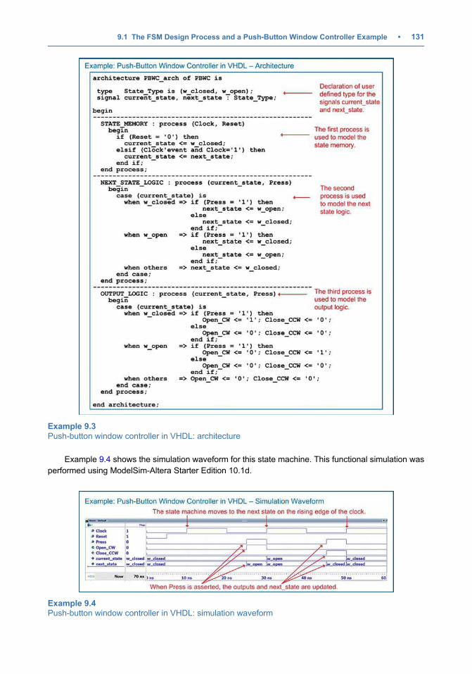
Example 9.4 shows the simulation waveform for this state machine. This functional simulation was
performed using ModelSim-Altera Starter Edition 10.1d.
Example 9.3Push-button window controller in VHDL: architecture
Example 9.4Push-button window controller in VHDL: simulation waveform
9.1 The FSM Design Process and a Push-Button Window Controller Example • 131
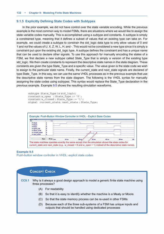
9.1.5 Explicitly Defining State Codes with Subtypes
In the prior example, we did not have control over the state variable encoding. While the previous
example is the most common way to model FSMs, there are situations where we would like to assign the
state variable codes manually. This is accomplished using a subtype and constants. A subtype is simply
a constrained type, meaning that it defines a subset of values that an existing type can take on. For
example, we could create a subtype to constrain the std_logic data type to only allow values of 0 and
1 and not the values of U, X, Z, W, L, H, and -. This would not be considered a new type since it is simply a
constraint put upon the existing std_logic type. A subtype defines the constraint and has a unique name
that can be used to declare other signals. To use this approach for manually encoding the states of a
FSM, we first declare a new subtype called State_Type that is simply a version of the existing type
std_logic. We then create constants to represent the descriptive state names in the state diagram. These
constants are given the type State_Type and a specific value. The value given is the state code we wish
to assign to the particular state name. Finally, the current_state and next_state signals are declared of
type State_Type. In this way, we can use the same VHDL processes as in the previous example that use
the descriptive state names from the state diagram. The following is the VHDL syntax for manually
assigning the state codes using subtypes. This syntax would replace the State_Type declaration in the
previous example. Example 9.5 shows the resulting simulation waveforms.
subtype State_Type is std_logic;
constant w_open : State_Type :¼ ‘0’;
constant w_closed : State_Type :¼ ‘1’;
signal current_state, next_state : State_Type;
CONCEPT CHECK
CC9.1 Why is it always a good design approach to model a generic finite state machine usingthree processes?
(A) For readability
(B) So that it is easy to identify whether the machine is a Mealy or Moore
(C) So that the state memory process can be re-used in other FSMs
(D) Because each of the three sub-systems of a FSM has unique inputs andoutputs that should be handled using dedicated processes
Example 9.5Push-button window controller in VHDL: explicit state codes
132 • Chapter 9: Modeling Finite State Machines
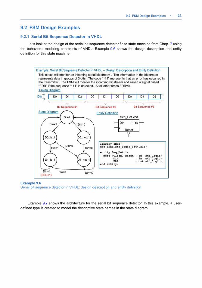
9.2 FSM Design Examples
9.2.1 Serial Bit Sequence Detector in VHDL
Let’s look at the design of the serial bit sequence detector finite state machine from Chap. 7 using
the behavioral modeling constructs of VHDL. Example 9.6 shows the design description and entity
definition for this state machine.
Example 9.7 shows the architecture for the serial bit sequence detector. In this example, a user-
defined type is created to model the descriptive state names in the state diagram.
Example 9.6Serial bit sequence detector in VHDL: design description and entity definition
9.2 FSM Design Examples • 133
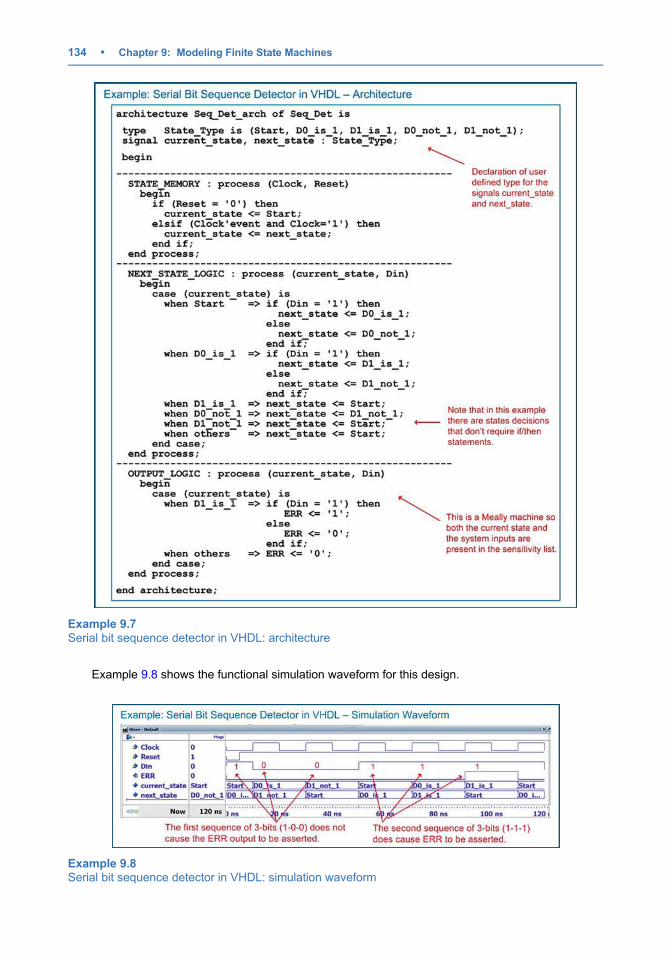
Example 9.8 shows the functional simulation waveform for this design.
Example 9.7Serial bit sequence detector in VHDL: architecture
Example 9.8Serial bit sequence detector in VHDL: simulation waveform
134 • Chapter 9: Modeling Finite State Machines
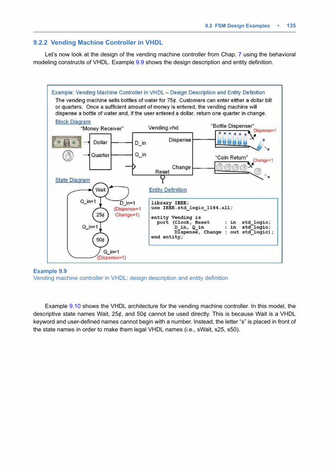
9.2.2 Vending Machine Controller in VHDL
Let’s now look at the design of the vending machine controller from Chap. 7 using the behavioral
modeling constructs of VHDL. Example 9.9 shows the design description and entity definition.
Example 9.10 shows the VHDL architecture for the vending machine controller. In this model, the
descriptive state names Wait, 25¢, and 50¢ cannot be used directly. This is because Wait is a VHDL
keyword and user-defined names cannot begin with a number. Instead, the letter “s” is placed in front of
the state names in order to make them legal VHDL names (i.e., sWait, s25, s50).
Example 9.9Vending machine controller in VHDL: design description and entity definition
9.2 FSM Design Examples • 135
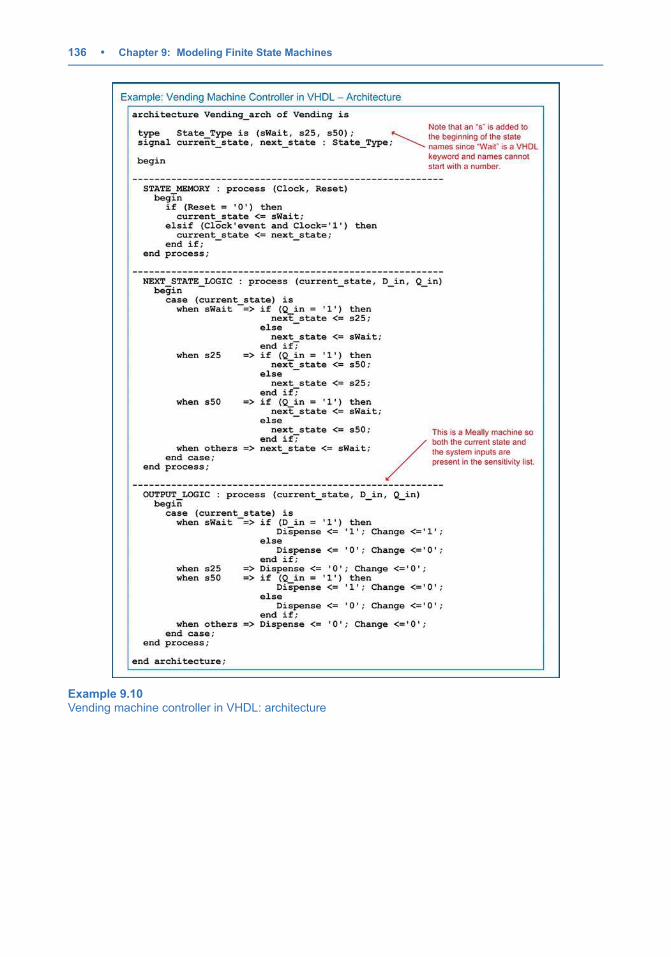
Example 9.10Vending machine controller in VHDL: architecture
136 • Chapter 9: Modeling Finite State Machines
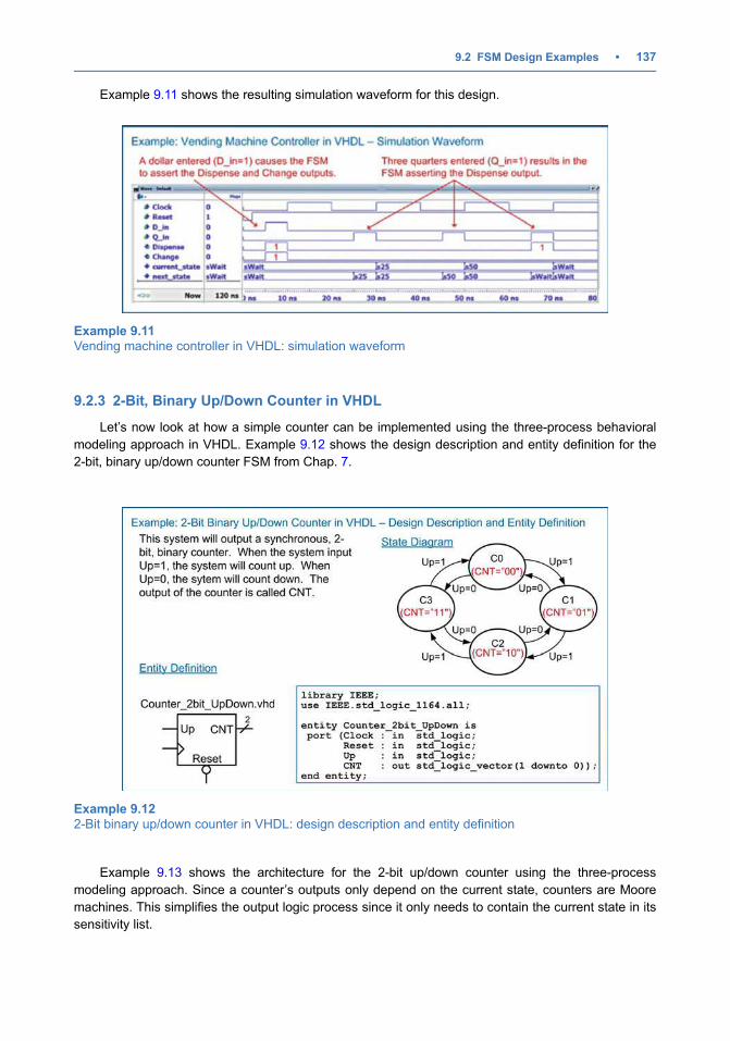
Example 9.11 shows the resulting simulation waveform for this design.
9.2.3 2-Bit, Binary Up/Down Counter in VHDL
Let’s now look at how a simple counter can be implemented using the three-process behavioral
modeling approach in VHDL. Example 9.12 shows the design description and entity definition for the
2-bit, binary up/down counter FSM from Chap. 7.
Example 9.13 shows the architecture for the 2-bit up/down counter using the three-process
modeling approach. Since a counter’s outputs only depend on the current state, counters are Moore
machines. This simplifies the output logic process since it only needs to contain the current state in its
sensitivity list.
Example 9.11Vending machine controller in VHDL: simulation waveform
Example 9.122-Bit binary up/down counter in VHDL: design description and entity definition
9.2 FSM Design Examples • 137
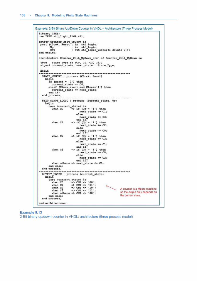
Example 9.132-Bit binary up/down counter in VHDL: architecture (three process model)
138 • Chapter 9: Modeling Finite State Machines
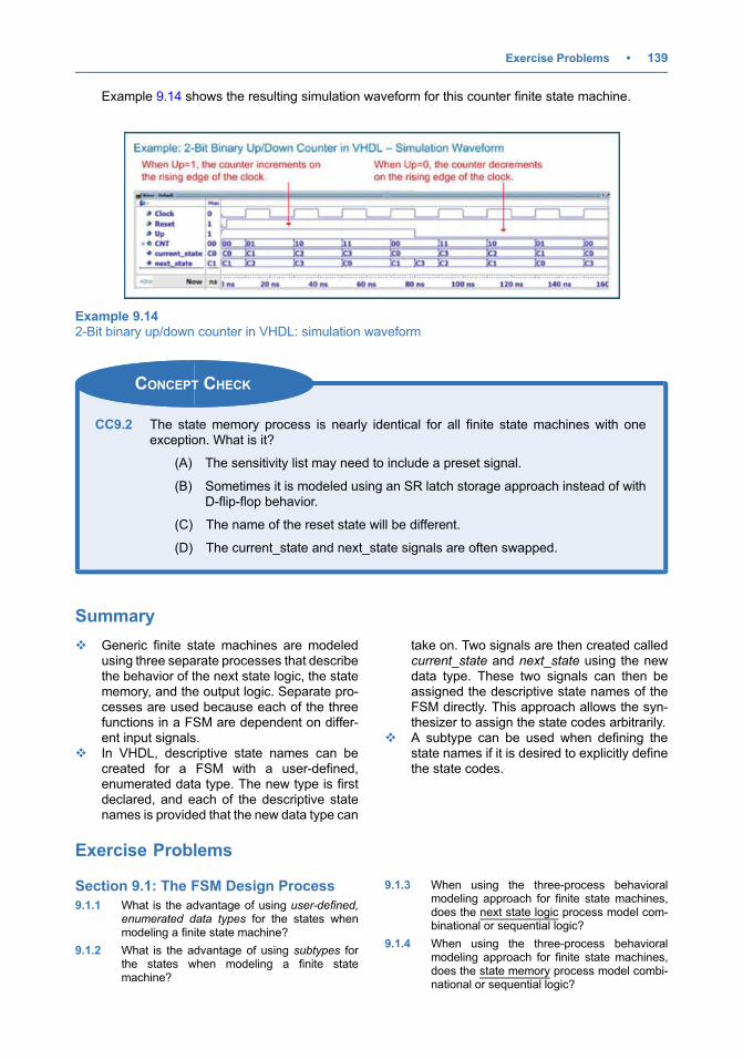
Example 9.14 shows the resulting simulation waveform for this counter finite state machine.
CONCEPT CHECK
CC9.2 The state memory process is nearly identical for all finite state machines with oneexception. What is it?
(A) The sensitivity list may need to include a preset signal.
(B) Sometimes it is modeled using an SR latch storage approach instead of withD-flip-flop behavior.
(C) The name of the reset state will be different.
(D) The current_state and next_state signals are often swapped.
Summary
v Generic finite state machines are modeledusing three separate processes that describethe behavior of the next state logic, the statememory, and the output logic. Separate pro-cesses are used because each of the threefunctions in a FSM are dependent on differ-ent input signals.
v In VHDL, descriptive state names can becreated for a FSM with a user-defined,enumerated data type. The new type is firstdeclared, and each of the descriptive statenames is provided that the new data type can
take on. Two signals are then created calledcurrent_state and next_state using the newdata type. These two signals can then beassigned the descriptive state names of theFSM directly. This approach allows the syn-thesizer to assign the state codes arbitrarily.
v A subtype can be used when defining thestate names if it is desired to explicitly definethe state codes.
Exercise Problems
Section 9.1: The FSM Design Process
9.1.1 What is the advantage of using user-defined,enumerated data types for the states whenmodeling a finite state machine?
9.1.2 What is the advantage of using subtypes forthe states when modeling a finite statemachine?
9.1.3 When using the three-process behavioralmodeling approach for finite state machines,does the next state logic process model com-binational or sequential logic?
9.1.4 When using the three-process behavioralmodeling approach for finite state machines,does the state memory process model combi-national or sequential logic?
Example 9.142-Bit binary up/down counter in VHDL: simulation waveform
Exercise Problems • 139
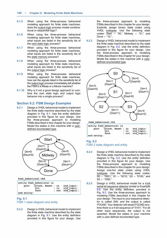
9.1.5 When using the three-process behavioralmodeling approach for finite state machines,does the output logic process model combina-tional or sequential logic?
9.1.6 When using the three-process behavioralmodeling approach for finite state machines,what inputs are listed in the sensitivity list ofthe next state logic process?
9.1.7 When using the three-process behavioralmodeling approach for finite state machines,what inputs are listed in the sensitivity list ofthe state memory process?
9.1.8 When using the three-process behavioralmodeling approach for finite state machines,what inputs are listed in the sensitivity list ofthe output logic process?
9.1.9 When using the three-process behavioralmodeling approach for finite state machines,how can the signals listed in the sensitivity list ofthe output logic process immediately tell whetherthe FSM is a Mealy or a Moore machine?
9.1.10 Why is it not a good design approach to com-bine the next state logic and output logicbehavior into a single process?
Section 9.2: FSM Design Examples
9.2.1 Design a VHDL behavioral model to implementthe finite state machine described by the statediagram in Fig. 9.1. Use the entity definitionprovided in this figure for your design. Usethe three-process approach to modelingFSMs described in this chapter for your design.Model the states in this machine with a user-defined enumerated type.
Fig. 9.1FSM 1 state diagram and entity
9.2.2 Design a VHDL behavioral model to implementthe finite state machine described by the statediagram in Fig. 9.1. Use the entity definitionprovided in this figure for your design. Use
the three-process approach to modelingFSMs described in this chapter for your design.Explicitly assign binary state codes usingVHDL subtypes. Use the following statecodes: Start ¼ “00,” Midway ¼ “01,” andDone ¼ “10.”,
9.2.3 Design a VHDL behavioral model to implementthe finite state machine described by the statediagram in Fig. 9.2. Use the entity definitionprovided in this figure for your design. Usethe three-process approach to modelingFSMs described in this chapter for your design.Model the states in this machine with a user-defined enumerated type.
Fig. 9.2FSM 2 state diagram and entity
9.2.4 Design a VHDL behavioral model to implementthe finite state machine described by the statediagram in Fig. 9.2. Use the entity definitionprovided in this figure for your design. Usethe three-process approach to modelingFSMs described in this chapter for your design.Assign one-hot state codes using VHDLsubtypes. Use the following state codes:S0 ¼ “0001,” S1 ¼ “0010,” S2 ¼ “0100,” andS3 ¼ “1000.”
9.2.5 Design a VHDL behavioral model for a 4-bitserial bit sequence detector similar to Example9.6. Use the entity definition provided inFig. 9.3. Use the three-process approach tomodeling FSMs described in this chapter foryour design. The input to your sequence detec-tor is called DIN, and the output is calledFOUND. Your detector will assert FOUND any-time there is a 4-bit sequence of “0101.” For allother input sequences, the output is notasserted. Model the states in your machinewith a user-defined enumerated type.
140 • Chapter 9: Modeling Finite State Machines
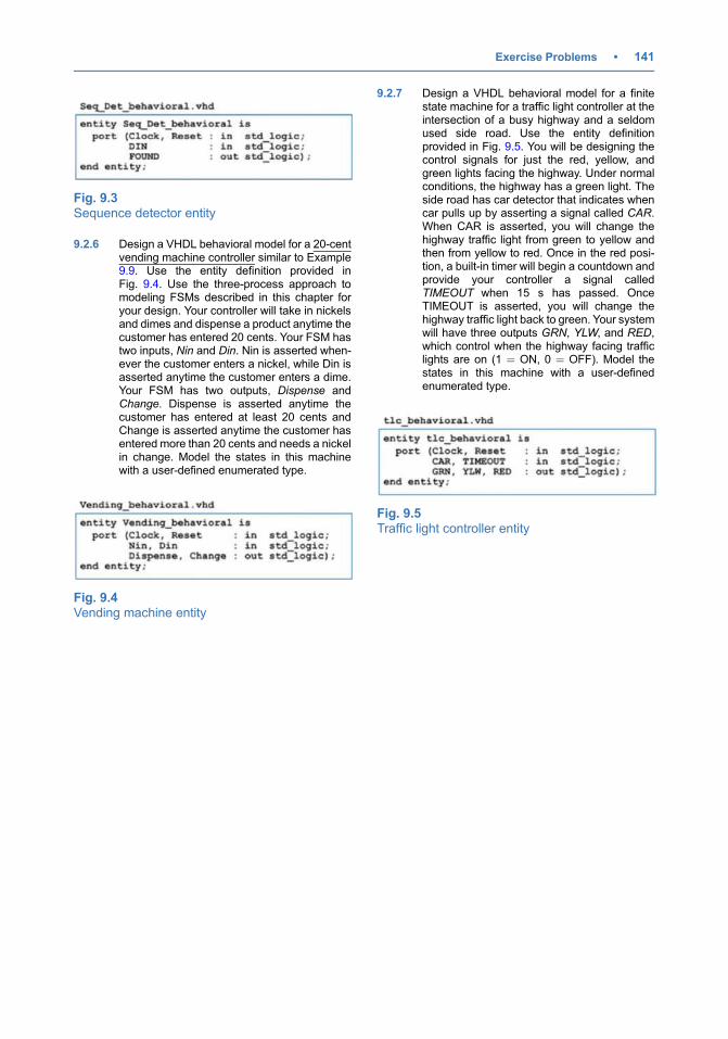
Fig. 9.3Sequence detector entity
9.2.6 Design a VHDL behavioral model for a 20-centvending machine controller similar to Example9.9. Use the entity definition provided inFig. 9.4. Use the three-process approach tomodeling FSMs described in this chapter foryour design. Your controller will take in nickelsand dimes and dispense a product anytime thecustomer has entered 20 cents. Your FSM hastwo inputs, Nin and Din. Nin is asserted when-ever the customer enters a nickel, while Din isasserted anytime the customer enters a dime.Your FSM has two outputs, Dispense andChange. Dispense is asserted anytime thecustomer has entered at least 20 cents andChange is asserted anytime the customer hasentered more than 20 cents and needs a nickelin change. Model the states in this machinewith a user-defined enumerated type.
Fig. 9.4Vending machine entity
9.2.7 Design a VHDL behavioral model for a finitestate machine for a traffic light controller at theintersection of a busy highway and a seldomused side road. Use the entity definitionprovided in Fig. 9.5. You will be designing thecontrol signals for just the red, yellow, andgreen lights facing the highway. Under normalconditions, the highway has a green light. Theside road has car detector that indicates whencar pulls up by asserting a signal called CAR.When CAR is asserted, you will change thehighway traffic light from green to yellow andthen from yellow to red. Once in the red posi-tion, a built-in timer will begin a countdown andprovide your controller a signal calledTIMEOUT when 15 s has passed. OnceTIMEOUT is asserted, you will change thehighway traffic light back to green. Your systemwill have three outputs GRN, YLW, and RED,which control when the highway facing trafficlights are on (1 ¼ ON, 0 ¼ OFF). Model thestates in this machine with a user-definedenumerated type.
Fig. 9.5Traffic light controller entity
Exercise Problems • 141
Chapter 10: Modeling CountersCounters are a special case of finite state machines because they move linearly through their
discrete states (either forward or backward) and typically are implemented with state-encoded outputs.
Due to this simplified structure and widespread use in digital systems, VHDL allows counters to be
modeled using a single process and with arithmetic operators (i.e., + and �). This enables a more
compact model and allows much wider counters to be implemented. This chapter will cover some of the
most common techniques for modeling counters.
Learning Outcomes—After completing this chapter, you will be able to:
10.1 Design a behavioral model for a counter using a single process.10.2 Design a behavioral model for a counter with enable and load capability.
10.1 Modeling Counters with a Single Process
10.1.1 Counters in VHDL Using the Type UNSIGNED
Let’s look at how we can model a 4-bit, binary up counter with an output called CNT. First, we want
to model this counter using the “+” operator. Recall that the “+” operator is not defined in the
std_logic_1164 package. We need to include the numeric_std package in order to add this capability.
Within the numeric_std package, the “+” operator is only defined for types signed and unsigned (and not
for std_logic_vector), so the output CNT will be declared as type unsigned. Next, we want to implement
the counter using a signal assignment in the form CNT <¼ CNT + 1; however, since CNT is an output
port, it cannot be used as an argument (right hand side) in an operation. We will need to create an internal
signal to implement the counter functionality (i.e., CNT_tmp). Since a signal does not contain direction-
ality, it can be used as both the target and an argument of an operation. Outside of the counter process, a
concurrent signal assignment is used to continuously assign CNT_tmp to CNT in order to drive the output
of the system. This means that we need to create the internal signal CNT_tmp of type unsigned also to
support this assignment. Example 10.1 shows the VHDL model and simulation waveform for this
counter. When the counter reaches its maximum value of “1111,” it rolls over to “0000” and continues
counting because it is defined to only contain 4 bits.
# Springer Nature Switzerland AG 2019
B. J. LaMeres, Quick Start Guide to VHDL, https://doi.org/10.1007/978-3-030-04516-6_10
143
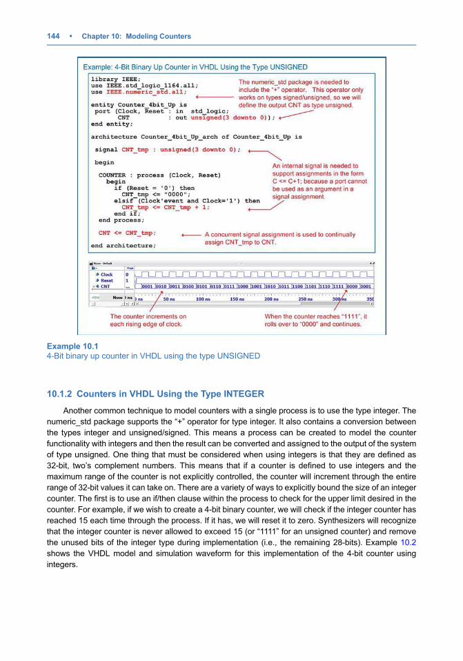
10.1.2 Counters in VHDL Using the Type INTEGER
Another common technique to model counters with a single process is to use the type integer. The
numeric_std package supports the “+” operator for type integer. It also contains a conversion between
the types integer and unsigned/signed. This means a process can be created to model the counter
functionality with integers and then the result can be converted and assigned to the output of the system
of type unsigned. One thing that must be considered when using integers is that they are defined as
32-bit, two’s complement numbers. This means that if a counter is defined to use integers and the
maximum range of the counter is not explicitly controlled, the counter will increment through the entire
range of 32-bit values it can take on. There are a variety of ways to explicitly bound the size of an integer
counter. The first is to use an if/then clause within the process to check for the upper limit desired in the
counter. For example, if we wish to create a 4-bit binary counter, we will check if the integer counter has
reached 15 each time through the process. If it has, we will reset it to zero. Synthesizers will recognize
that the integer counter is never allowed to exceed 15 (or “1111” for an unsigned counter) and remove
the unused bits of the integer type during implementation (i.e., the remaining 28-bits). Example 10.2
shows the VHDL model and simulation waveform for this implementation of the 4-bit counter using
integers.
Example 10.14-Bit binary up counter in VHDL using the type UNSIGNED
144 • Chapter 10: Modeling Counters
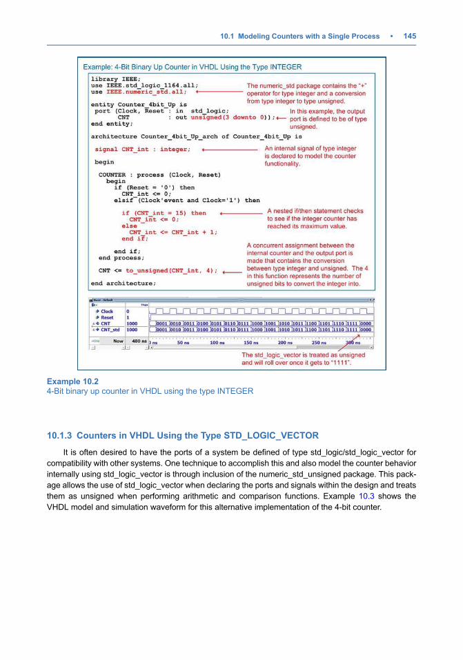
10.1.3 Counters in VHDL Using the Type STD_LOGIC_VECTOR
It is often desired to have the ports of a system be defined of type std_logic/std_logic_vector for
compatibility with other systems. One technique to accomplish this and also model the counter behavior
internally using std_logic_vector is through inclusion of the numeric_std_unsigned package. This pack-
age allows the use of std_logic_vector when declaring the ports and signals within the design and treats
them as unsigned when performing arithmetic and comparison functions. Example 10.3 shows the
VHDL model and simulation waveform for this alternative implementation of the 4-bit counter.
Example 10.24-Bit binary up counter in VHDL using the type INTEGER
10.1 Modeling Counters with a Single Process • 145
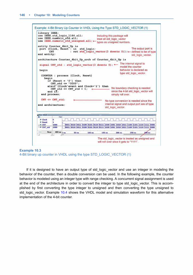
If it is designed to have an output type of std_logic_vector and use an integer in modeling the
behavior of the counter, then a double conversion can be used. In the following example, the counter
behavior is modeled using an integer type with range checking. A concurrent signal assignment is used
at the end of the architecture in order to convert the integer to type std_logic_vector. This is accom-
plished by first converting the type integer to unsigned and then converting the type unsigned to
std_logic_vector. Example 10.4 shows the VHDL model and simulation waveform for this alternative
implementation of the 4-bit counter.
Example 10.34-Bit binary up counter in VHDL using the type STD_LOGIC_VECTOR (1)
146 • Chapter 10: Modeling Counters
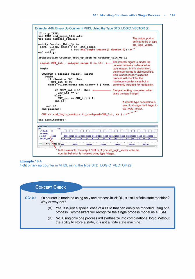
CONCEPT CHECK
CC10.1 If a counter is modeled using only one process in VHDL, is it still a finite state machine?Why or why not?
(A) Yes. It is just a special case of a FSM that can easily be modeled using oneprocess. Synthesizers will recognize the single process model as a FSM.
(B) No. Using only one process will synthesize into combinational logic. Withoutthe ability to store a state, it is not a finite state machine.
Example 10.44-Bit binary up counter in VHDL using the type STD_LOGIC_VECTOR (2)
10.1 Modeling Counters with a Single Process • 147
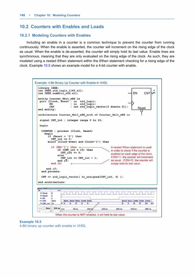
10.2 Counters with Enables and Loads
10.2.1 Modeling Counters with Enables
Including an enable in a counter is a common technique to prevent the counter from running
continuously. When the enable is asserted, the counter will increment on the rising edge of the clock
as usual. When the enable is de-asserted, the counter will simply hold its last value. Enable lines are
synchronous, meaning that they are only evaluated on the rising edge of the clock. As such, they are
modeled using a nested if/then statement within the if/then statement checking for a rising edge of the
clock. Example 10.5 shows an example model for a 4-bit counter with enable.
Example 10.54-Bit binary up counter with enable in VHDL
148 • Chapter 10: Modeling Counters
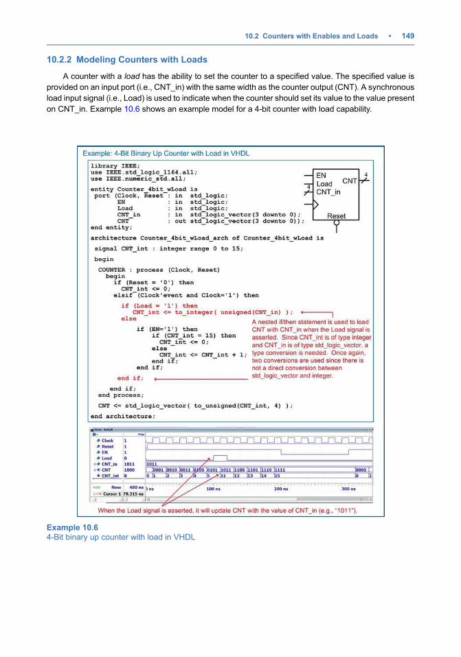
10.2.2 Modeling Counters with Loads
A counter with a load has the ability to set the counter to a specified value. The specified value is
provided on an input port (i.e., CNT_in) with the same width as the counter output (CNT). A synchronous
load input signal (i.e., Load) is used to indicate when the counter should set its value to the value present
on CNT_in. Example 10.6 shows an example model for a 4-bit counter with load capability.
Example 10.64-Bit binary up counter with load in VHDL
10.2 Counters with Enables and Loads • 149
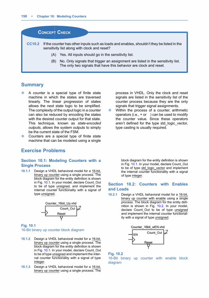
CONCEPT CHECK
CC10.2 If the counter has other inputs such as loads and enables, shouldn’t they be listed in thesensitivity list along with clock and reset?
(A) Yes. All inputs should go in the sensitivity list.
(B) No. Only signals that trigger an assignment are listed in the sensitivity list.The only two signals that have this behavior are clock and reset.
Summary
v A counter is a special type of finite statemachine in which the states are traversedlinearly. The linear progression of statesallows the next state logic to be simplified.The complexity of the output logic in a countercan also be reduced by encoding the stateswith the desired counter output for that state.This technique, known as state-encoded
outputs, allows the system outputs to simplybe the current state of the FSM.
v Counters are a special type of finite statemachine that can be modeled using a single
process in VHDL. Only the clock and resetsignals are listed in the sensitivity list of thecounter process because they are the onlysignals that trigger signal assignments.
v Within the process of a counter, arithmeticoperators (i.e., + or �) can be used to modifythe counter value. Since these operatorsaren’t defined for the type std_logic_vector,type casting is usually required.
Exercise Problems
Section 10.1: Modeling Counters with a
Single Process
10.1.1 Design a VHDL behavioral model for a 16-bit,binary up counter using a single process. Theblock diagram for the entity definition is shownin Fig. 10.1. In your model, declare Count_Outto be of type unsigned, and implement theinternal counter functionality with a signal oftype unsigned.
Fig. 10.116-Bit binary up counter block diagram
10.1.2 Design a VHDL behavioral model for a 16-bit,binary up counter using a single process. Theblock diagram for the entity definition is shownin Fig. 10.1. In your model, declare Count_Outto be of type unsigned and implement the inter-nal counter functionality with a signal of typeinteger.
10.1.3 Design a VHDL behavioral model for a 16-bit,binary up counter using a single process. The
block diagram for the entity definition is shownin Fig. 10.1. In your model, declare Count_Outto be of type std_logic_vector and implementthe internal counter functionality with a signalof type integer.
Section 10.2: Counters with Enables
and Loads
10.2.1 Design a VHDL behavioral model for a 16-bit,binary up counter with enable using a singleprocess. The block diagram for the entity defi-nition is shown in Fig. 10.2. In your model,declare Count_Out to be of type unsignedand implement the internal counter functional-ity with a signal of type unsigned.
Fig. 10.216-Bit binary up counter with enable blockdiagram
150 • Chapter 10: Modeling Counters
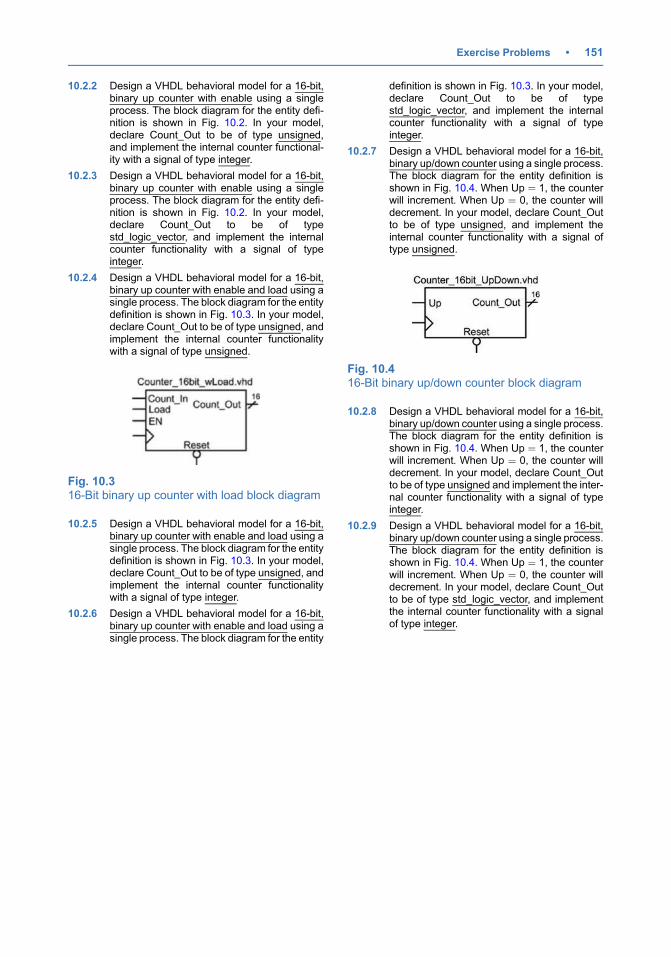
10.2.2 Design a VHDL behavioral model for a 16-bit,binary up counter with enable using a singleprocess. The block diagram for the entity defi-nition is shown in Fig. 10.2. In your model,declare Count_Out to be of type unsigned,and implement the internal counter functional-ity with a signal of type integer.
10.2.3 Design a VHDL behavioral model for a 16-bit,binary up counter with enable using a singleprocess. The block diagram for the entity defi-nition is shown in Fig. 10.2. In your model,declare Count_Out to be of typestd_logic_vector, and implement the internalcounter functionality with a signal of typeinteger.
10.2.4 Design a VHDL behavioral model for a 16-bit,binary up counter with enable and load using asingle process. The block diagram for the entitydefinition is shown in Fig. 10.3. In your model,declare Count_Out to be of type unsigned, andimplement the internal counter functionalitywith a signal of type unsigned.
Fig. 10.316-Bit binary up counter with load block diagram
10.2.5 Design a VHDL behavioral model for a 16-bit,binary up counter with enable and load using asingle process. The block diagram for the entitydefinition is shown in Fig. 10.3. In your model,declare Count_Out to be of type unsigned, andimplement the internal counter functionalitywith a signal of type integer.
10.2.6 Design a VHDL behavioral model for a 16-bit,binary up counter with enable and load using asingle process. The block diagram for the entity
definition is shown in Fig. 10.3. In your model,declare Count_Out to be of typestd_logic_vector, and implement the internalcounter functionality with a signal of typeinteger.
10.2.7 Design a VHDL behavioral model for a 16-bit,binary up/down counter using a single process.The block diagram for the entity definition isshown in Fig. 10.4. When Up ¼ 1, the counterwill increment. When Up ¼ 0, the counter willdecrement. In your model, declare Count_Outto be of type unsigned, and implement theinternal counter functionality with a signal oftype unsigned.
Fig. 10.416-Bit binary up/down counter block diagram
10.2.8 Design a VHDL behavioral model for a 16-bit,binary up/down counter using a single process.The block diagram for the entity definition isshown in Fig. 10.4. When Up ¼ 1, the counterwill increment. When Up ¼ 0, the counter willdecrement. In your model, declare Count_Outto be of type unsigned and implement the inter-nal counter functionality with a signal of typeinteger.
10.2.9 Design a VHDL behavioral model for a 16-bit,binary up/down counter using a single process.The block diagram for the entity definition isshown in Fig. 10.4. When Up ¼ 1, the counterwill increment. When Up ¼ 0, the counter willdecrement. In your model, declare Count_Outto be of type std_logic_vector, and implementthe internal counter functionality with a signalof type integer.
Exercise Problems • 151
Chapter 11: Modeling MemoryThis chapter covers how to model memory arrays in VHDL. These models are technology indepen-
dent, meaning that they can be ultimately synthesized into a wide range of semiconductor memory
devices.
Learning Outcomes—After completing this chapter, you will be able to:
11.1 Describe the basic architecture and terminology for semiconductor-based memorysystems.
11.2 Design a VHDL model for a read-only memory array.11.3 Design a VHDL model for a read/write memory array.
11.1 Memory Architecture and Terminology
The termmemory is used to describe a system with the ability to store digital information. The term
semiconductor memory refers to systems that are implemented using integrated circuit technology.
These types of systems store the digital information using transistors, fuses, and/or capacitors on a
single semiconductor substrate. Memory can also be implemented using technology other than
semiconductors. Disk drives store information by altering the polarity of magnetic fields on a circular
substrate. The two magnetic polarities (north and south) are used to represent different logic values (i.e.,
0 or 1). Optical disks use lasers to burn pits into reflective substrates. The binary information is
represented by light either being reflected (no pit) or not reflected (pit present). Semiconductor memory
does not have any moving parts, so it is called solid state memory and can hold more information per unit
area than disk memory. Regardless of the technology used to store the binary data, all memory has
common attributes and terminology that are discussed in this chapter.
11.1.1 Memory Map Model
The information stored in memory is called the data. When information is placed into memory, it is
called a write. When information is retrieved from memory, it is called a read. In order to access data in
memory, an address is used. While data can be accessed as individual bits, in order to reduce the
number of address locations needed, data is typically grouped into N-bit words. If a memory system has
N ¼ 8, this means that 8-bits of data are stored at each address. The number of address locations is
described using the variableM. The overall size of the memory is typically stated by saying “M � N.” For
example, if we had a 16 � 8 memory system, that means that there are 16 address locations, each
capable of storing a byte of data. This memory would have a capacity of 16 � 8 ¼ 128 bits. Since the
address is implemented as a binary code, the number of lines in the address bus (n) will dictate the
number of address locations that the memory system will have (M ¼ 2n). Figure 11.1 shows a graphical
depiction of how data resides in memory. This type of graphic is called a memory map model.
# Springer Nature Switzerland AG 2019
B. J. LaMeres, Quick Start Guide to VHDL, https://doi.org/10.1007/978-3-030-04516-6_11
153
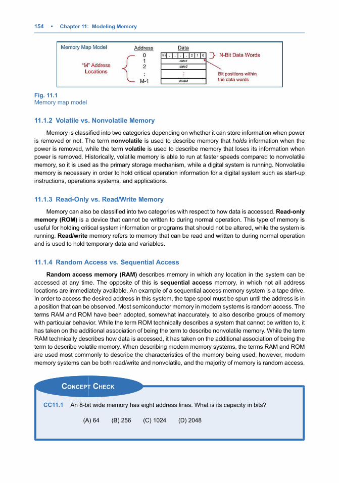
11.1.2 Volatile vs. Nonvolatile Memory
Memory is classified into two categories depending on whether it can store information when power
is removed or not. The term nonvolatile is used to describe memory that holds information when the
power is removed, while the term volatile is used to describe memory that loses its information when
power is removed. Historically, volatile memory is able to run at faster speeds compared to nonvolatile
memory, so it is used as the primary storage mechanism, while a digital system is running. Nonvolatile
memory is necessary in order to hold critical operation information for a digital system such as start-up
instructions, operations systems, and applications.
11.1.3 Read-Only vs. Read/Write Memory
Memory can also be classified into two categories with respect to how data is accessed. Read-only
memory (ROM) is a device that cannot be written to during normal operation. This type of memory is
useful for holding critical system information or programs that should not be altered, while the system is
running. Read/write memory refers to memory that can be read and written to during normal operation
and is used to hold temporary data and variables.
11.1.4 Random Access vs. Sequential Access
Random access memory (RAM) describes memory in which any location in the system can be
accessed at any time. The opposite of this is sequential access memory, in which not all address
locations are immediately available. An example of a sequential access memory system is a tape drive.
In order to access the desired address in this system, the tape spool must be spun until the address is in
a position that can be observed. Most semiconductor memory in modern systems is random access. The
terms RAM and ROM have been adopted, somewhat inaccurately, to also describe groups of memory
with particular behavior. While the term ROM technically describes a system that cannot be written to, it
has taken on the additional association of being the term to describe nonvolatile memory. While the term
RAM technically describes how data is accessed, it has taken on the additional association of being the
term to describe volatile memory. When describing modern memory systems, the terms RAM and ROM
are used most commonly to describe the characteristics of the memory being used; however, modern
memory systems can be both read/write and nonvolatile, and the majority of memory is random access.
CONCEPT CHECK
CC11.1 An 8-bit wide memory has eight address lines. What is its capacity in bits?
(A) 64 (B) 256 (C) 1024 (D) 2048
Fig. 11.1Memory map model
154 • Chapter 11: Modeling Memory
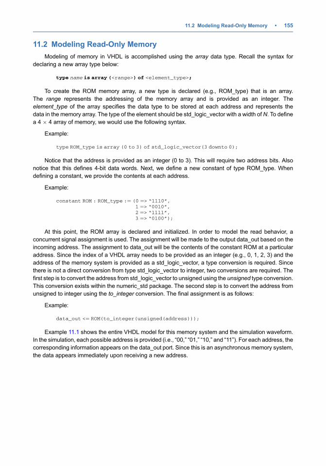
11.2 Modeling Read-Only Memory
Modeling of memory in VHDL is accomplished using the array data type. Recall the syntax for
declaring a new array type below:
type name is array (<range>) of <element_type>;
To create the ROM memory array, a new type is declared (e.g., ROM_type) that is an array.
The range represents the addressing of the memory array and is provided as an integer. The
element_type of the array specifies the data type to be stored at each address and represents the
data in the memory array. The type of the element should be std_logic_vector with a width of N. To define
a 4 � 4 array of memory, we would use the following syntax.
Example:
type ROM_type is array (0 to 3) of std_logic_vector(3 downto 0);
Notice that the address is provided as an integer (0 to 3). This will require two address bits. Also
notice that this defines 4-bit data words. Next, we define a new constant of type ROM_type. When
defining a constant, we provide the contents at each address.
Example:
constant ROM : ROM_type :¼ (0 ¼> “1110”,
1 ¼> “0010”,
2 ¼> “1111”,
3 ¼> “0100”);
At this point, the ROM array is declared and initialized. In order to model the read behavior, a
concurrent signal assignment is used. The assignment will be made to the output data_out based on the
incoming address. The assignment to data_out will be the contents of the constant ROM at a particular
address. Since the index of a VHDL array needs to be provided as an integer (e.g., 0, 1, 2, 3) and the
address of the memory system is provided as a std_logic_vector, a type conversion is required. Since
there is not a direct conversion from type std_logic_vector to integer, two conversions are required. The
first step is to convert the address from std_logic_vector to unsigned using the unsigned type conversion.
This conversion exists within the numeric_std package. The second step is to convert the address from
unsigned to integer using the to_integer conversion. The final assignment is as follows:
Example:
data_out <¼ ROM(to_integer(unsigned(address)));
Example 11.1 shows the entire VHDL model for this memory system and the simulation waveform.
In the simulation, each possible address is provided (i.e., “00,” “01,” “10,” and “11”). For each address, the
corresponding information appears on the data_out port. Since this is an asynchronous memory system,
the data appears immediately upon receiving a new address.
11.2 Modeling Read-Only Memory • 155
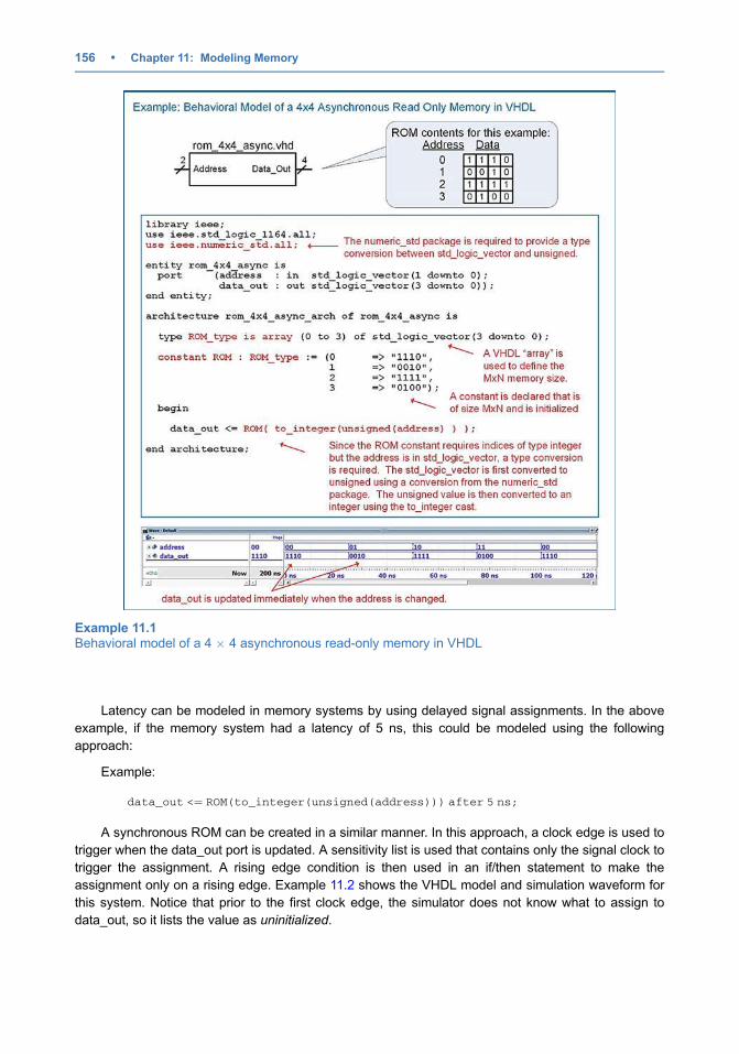
Latency can be modeled in memory systems by using delayed signal assignments. In the above
example, if the memory system had a latency of 5 ns, this could be modeled using the following
approach:
Example:
data_out <¼ ROM(to_integer(unsigned(address))) after 5 ns;
A synchronous ROM can be created in a similar manner. In this approach, a clock edge is used to
trigger when the data_out port is updated. A sensitivity list is used that contains only the signal clock to
trigger the assignment. A rising edge condition is then used in an if/then statement to make the
assignment only on a rising edge. Example 11.2 shows the VHDL model and simulation waveform for
this system. Notice that prior to the first clock edge, the simulator does not know what to assign to
data_out, so it lists the value as uninitialized.
Example 11.1Behavioral model of a 4 � 4 asynchronous read-only memory in VHDL
156 • Chapter 11: Modeling Memory
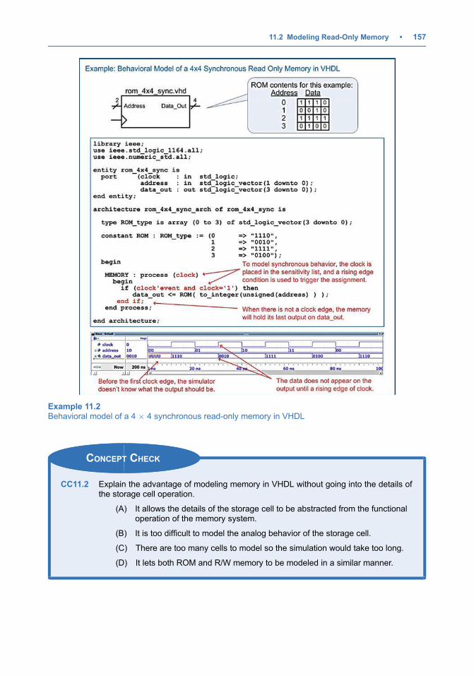
CONCEPT CHECK
CC11.2 Explain the advantage of modeling memory in VHDL without going into the details ofthe storage cell operation.
(A) It allows the details of the storage cell to be abstracted from the functionaloperation of the memory system.
(B) It is too difficult to model the analog behavior of the storage cell.
(C) There are too many cells to model so the simulation would take too long.
(D) It lets both ROM and R/W memory to be modeled in a similar manner.
Example 11.2Behavioral model of a 4 � 4 synchronous read-only memory in VHDL
11.2 Modeling Read-Only Memory • 157
11.3 Modeling Read/Write Memory
In a read/write memory model, a new type is created using a VHDL array (e.g., RW_type) that
defines the size of the storage system. To create the memory, a new signal is declared with the
array type.
Example:
type RW_type is array (0 to 3) std_logic_vector(3 downto 0);
signal RW : RW_type;
Note that a signal is used in a read/write system as opposed to a constant as in the read-only
memory system. This is because a read/write system is uninitialized until it is written to. A process is then
used to model the behavior of the memory system. Since this is an asynchronous system, all inputs are
listed in the sensitivity list (i.e., address, WE, and data_in). The process first checks whether the write
enable line is asserted (WE¼ 1), which indicates a write cycle is being performed. If it is, then it makes an
assignment to the RW signal at the location provided by the address input with the data provided by the
data_in input. Since the RWarray is indexed using integers, type conversions are required to convert the
address from std_logic_vector to integer. When WE is not asserted (WE ¼ 0), a read cycle is being
performed. In this case, the process makes an assignment to data_out with the contents stored at the
provided address. This assignment also requires type conversions to change the address from
std_logic_vector to integer. The following syntax implements this behavior:
Example:
MEMORY: process (address, WE, data_in)
begin
if (WE ¼ ’1’) then
RW(to_integer(unsigned(address))) <¼ data_in;
else
data_out <¼ RW(to_integer(unsigned(address)));
end if;
end process;
A read/write memory does not contain information until its storage locations are written to. As a
result, if the memory is read from before it has been written to, the simulation will return uninitialized.
Example 11.3 shows the entire VHDL model for an asynchronous read/write memory and the simulation
waveform showing read/write cycles.
158 • Chapter 11: Modeling Memory
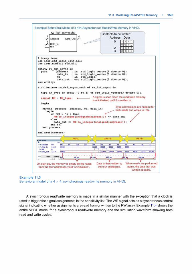
A synchronous read/write memory is made in a similar manner with the exception that a clock is
used to trigger the signal assignments in the sensitivity list. The WE signal acts as a synchronous control
signal indicating whether assignments are read from or written to the RWarray. Example 11.4 shows the
entire VHDL model for a synchronous read/write memory and the simulation waveform showing both
read and write cycles.
Example 11.3Behavioral model of a 4 � 4 asynchronous read/write memory in VHDL
11.3 Modeling Read/Write Memory • 159
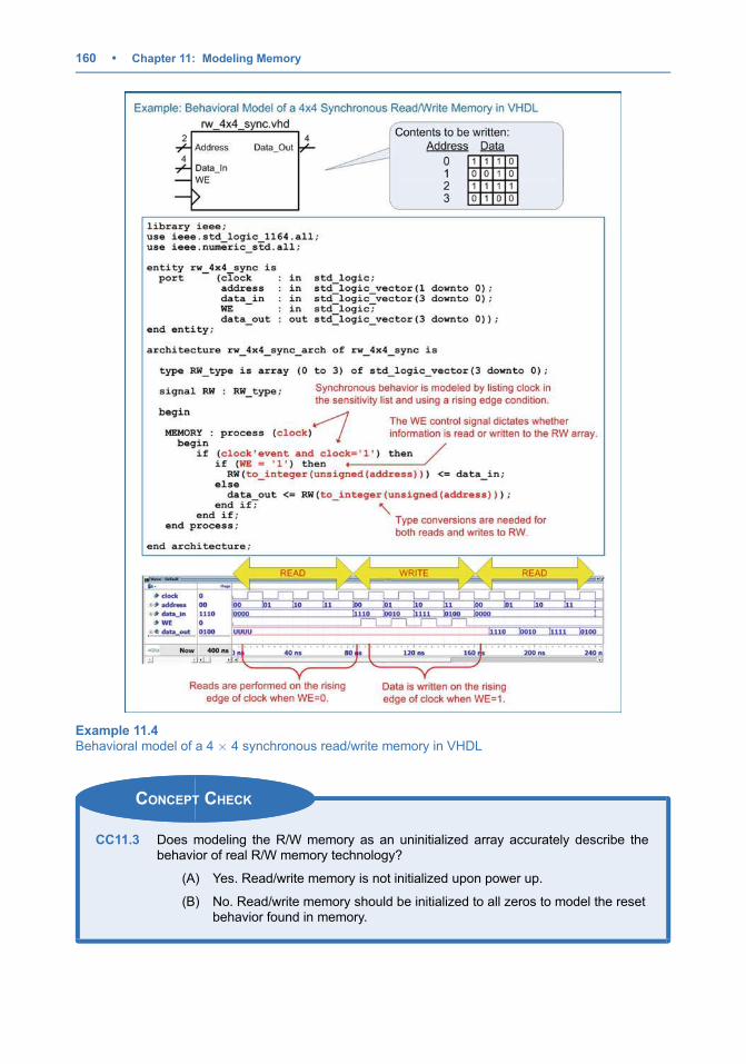
CONCEPT CHECK
CC11.3 Does modeling the R/W memory as an uninitialized array accurately describe thebehavior of real R/W memory technology?
(A) Yes. Read/write memory is not initialized upon power up.
(B) No. Read/write memory should be initialized to all zeros to model the resetbehavior found in memory.
Example 11.4Behavioral model of a 4 � 4 synchronous read/write memory in VHDL
160 • Chapter 11: Modeling Memory
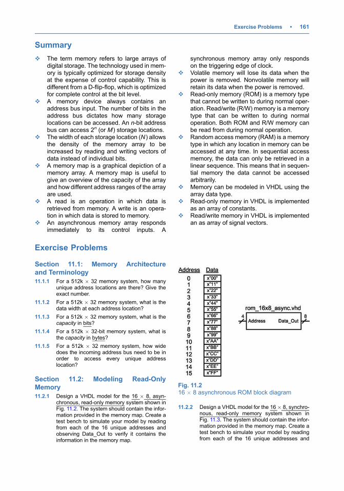
Summary
v The term memory refers to large arrays ofdigital storage. The technology used in mem-ory is typically optimized for storage densityat the expense of control capability. This isdifferent from a D-flip-flop, which is optimizedfor complete control at the bit level.
v A memory device always contains anaddress bus input. The number of bits in theaddress bus dictates how many storagelocations can be accessed. An n-bit addressbus can access 2n (or M ) storage locations.
v The width of each storage location (N ) allowsthe density of the memory array to beincreased by reading and writing vectors ofdata instead of individual bits.
v A memory map is a graphical depiction of amemory array. A memory map is useful togive an overview of the capacity of the arrayand how different address ranges of the arrayare used.
v A read is an operation in which data isretrieved from memory. A write is an opera-tion in which data is stored to memory.
v An asynchronous memory array respondsimmediately to its control inputs. A
synchronous memory array only respondson the triggering edge of clock.
v Volatile memory will lose its data when thepower is removed. Nonvolatile memory willretain its data when the power is removed.
v Read-only memory (ROM) is a memory typethat cannot be written to during normal oper-ation. Read/write (R/W) memory is a memorytype that can be written to during normaloperation. Both ROM and R/W memory canbe read from during normal operation.
v Random access memory (RAM) is a memorytype in which any location in memory can beaccessed at any time. In sequential accessmemory, the data can only be retrieved in alinear sequence. This means that in sequen-tial memory the data cannot be accessedarbitrarily.
v Memory can be modeled in VHDL using thearray data type.
v Read-only memory in VHDL is implementedas an array of constants.
v Read/write memory in VHDL is implementedan as array of signal vectors.
Exercise Problems
Section 11.1: Memory Architecture
and Terminology
11.1.1 For a 512k � 32 memory system, how manyunique address locations are there? Give theexact number.
11.1.2 For a 512k � 32 memory system, what is thedata width at each address location?
11.1.3 For a 512k � 32 memory system, what is thecapacity in bits?
11.1.4 For a 512k � 32-bit memory system, what isthe capacity in bytes?
11.1.5 For a 512k � 32 memory system, how widedoes the incoming address bus need to be inorder to access every unique addresslocation?
Section 11.2: Modeling Read-Only
Memory
11.2.1 Design a VHDL model for the 16 � 8, asyn-chronous, read-only memory system shown inFig. 11.2. The system should contain the infor-mation provided in the memory map. Create atest bench to simulate your model by readingfrom each of the 16 unique addresses andobserving Data_Out to verify it contains theinformation in the memory map.
Fig. 11.216 � 8 asynchronous ROM block diagram
11.2.2 Design a VHDL model for the 16 � 8, synchro-nous, read-only memory system shown inFig. 11.3. The system should contain the infor-mation provided in the memory map. Create atest bench to simulate your model by readingfrom each of the 16 unique addresses and
Exercise Problems • 161
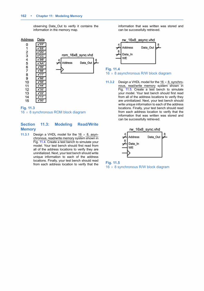
observing Data_Out to verify it contains theinformation in the memory map.
Fig. 11.316 � 8 synchronous ROM block diagram
Section 11.3: Modeling Read/Write
Memory
11.3.1 Design a VHDL model for the 16 � 8, asyn-chronous, read/write memory system shown inFig. 11.4. Create a test bench to simulate yourmodel. Your test bench should first read fromall of the address locations to verify they areuninitialized. Next, your test bench should writeunique information to each of the addresslocations. Finally, your test bench should readfrom each address location to verify that the
information that was written was stored andcan be successfully retrieved.
Fig. 11.416 � 8 asynchronous R/W block diagram
11.3.2 Design a VHDL model for the 16 � 8, synchro-nous, read/write memory system shown inFig. 11.5. Create a test bench to simulateyour model. Your test bench should first readfrom all of the address locations to verify theyare uninitialized. Next, your test bench shouldwrite unique information to each of the addresslocations. Finally, your test bench should readfrom each address location to verify that theinformation that was written was stored andcan be successfully retrieved.
Fig. 11.516 � 8 synchronous R/W block diagram
162 • Chapter 11: Modeling Memory
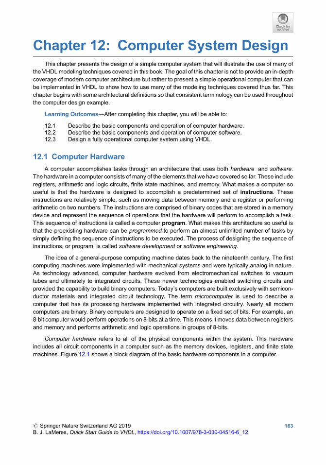
Chapter 12: Computer System DesignThis chapter presents the design of a simple computer system that will illustrate the use of many of
the VHDLmodeling techniques covered in this book. The goal of this chapter is not to provide an in-depth
coverage of modern computer architecture but rather to present a simple operational computer that can
be implemented in VHDL to show how to use many of the modeling techniques covered thus far. This
chapter begins with some architectural definitions so that consistent terminology can be used throughout
the computer design example.
Learning Outcomes—After completing this chapter, you will be able to:
12.1 Describe the basic components and operation of computer hardware.12.2 Describe the basic components and operation of computer software.12.3 Design a fully operational computer system using VHDL.
12.1 Computer Hardware
A computer accomplishes tasks through an architecture that uses both hardware and software.
The hardware in a computer consists of many of the elements that we have covered so far. These include
registers, arithmetic and logic circuits, finite state machines, and memory. What makes a computer so
useful is that the hardware is designed to accomplish a predetermined set of instructions. These
instructions are relatively simple, such as moving data between memory and a register or performing
arithmetic on two numbers. The instructions are comprised of binary codes that are stored in a memory
device and represent the sequence of operations that the hardware will perform to accomplish a task.
This sequence of instructions is called a computer program. What makes this architecture so useful is
that the preexisting hardware can be programmed to perform an almost unlimited number of tasks by
simply defining the sequence of instructions to be executed. The process of designing the sequence of
instructions, or program, is called software development or software engineering.
The idea of a general-purpose computing machine dates back to the nineteenth century. The first
computing machines were implemented with mechanical systems and were typically analog in nature.
As technology advanced, computer hardware evolved from electromechanical switches to vacuum
tubes and ultimately to integrated circuits. These newer technologies enabled switching circuits and
provided the capability to build binary computers. Today’s computers are built exclusively with semicon-
ductor materials and integrated circuit technology. The term microcomputer is used to describe a
computer that has its processing hardware implemented with integrated circuitry. Nearly all modern
computers are binary. Binary computers are designed to operate on a fixed set of bits. For example, an
8-bit computer would perform operations on 8-bits at a time. This means it moves data between registers
and memory and performs arithmetic and logic operations in groups of 8-bits.
Computer hardware refers to all of the physical components within the system. This hardware
includes all circuit components in a computer such as the memory devices, registers, and finite state
machines. Figure 12.1 shows a block diagram of the basic hardware components in a computer.
# Springer Nature Switzerland AG 2019
B. J. LaMeres, Quick Start Guide to VHDL, https://doi.org/10.1007/978-3-030-04516-6_12
163
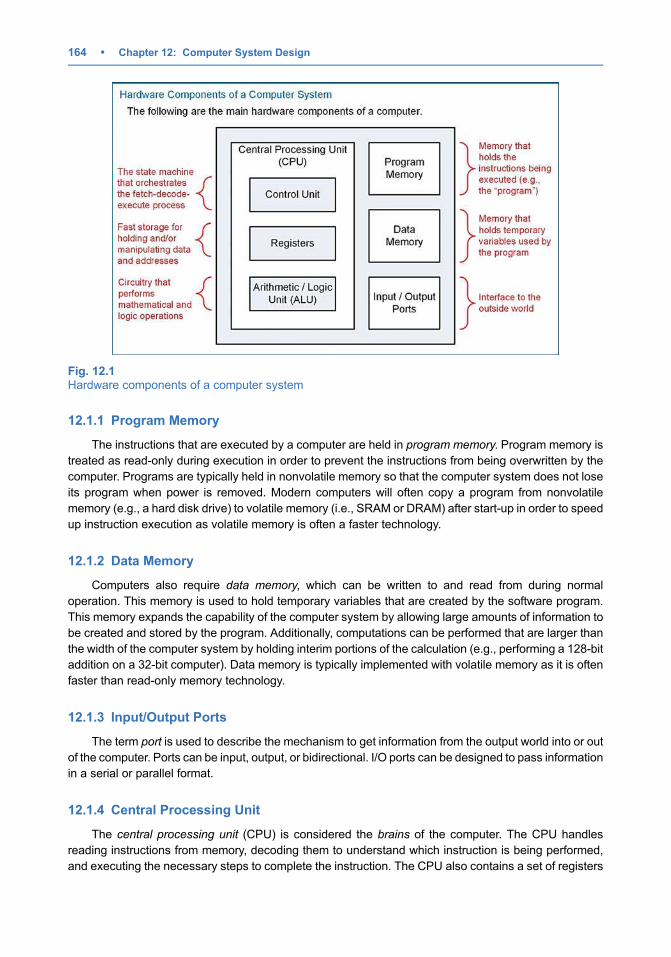
12.1.1 Program Memory
The instructions that are executed by a computer are held in program memory. Program memory is
treated as read-only during execution in order to prevent the instructions from being overwritten by the
computer. Programs are typically held in nonvolatile memory so that the computer system does not lose
its program when power is removed. Modern computers will often copy a program from nonvolatile
memory (e.g., a hard disk drive) to volatile memory (i.e., SRAM or DRAM) after start-up in order to speed
up instruction execution as volatile memory is often a faster technology.
12.1.2 Data Memory
Computers also require data memory, which can be written to and read from during normal
operation. This memory is used to hold temporary variables that are created by the software program.
This memory expands the capability of the computer system by allowing large amounts of information to
be created and stored by the program. Additionally, computations can be performed that are larger than
the width of the computer system by holding interim portions of the calculation (e.g., performing a 128-bit
addition on a 32-bit computer). Data memory is typically implemented with volatile memory as it is often
faster than read-only memory technology.
12.1.3 Input/Output Ports
The term port is used to describe the mechanism to get information from the output world into or out
of the computer. Ports can be input, output, or bidirectional. I/O ports can be designed to pass information
in a serial or parallel format.
12.1.4 Central Processing Unit
The central processing unit (CPU) is considered the brains of the computer. The CPU handles
reading instructions from memory, decoding them to understand which instruction is being performed,
and executing the necessary steps to complete the instruction. The CPU also contains a set of registers
Fig. 12.1Hardware components of a computer system
164 • Chapter 12: Computer System Design
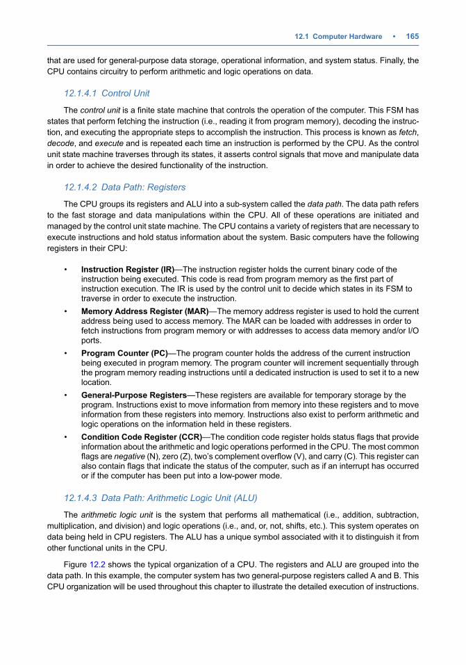
that are used for general-purpose data storage, operational information, and system status. Finally, the
CPU contains circuitry to perform arithmetic and logic operations on data.
12.1.4.1 Control Unit
The control unit is a finite state machine that controls the operation of the computer. This FSM has
states that perform fetching the instruction (i.e., reading it from program memory), decoding the instruc-
tion, and executing the appropriate steps to accomplish the instruction. This process is known as fetch,
decode, and execute and is repeated each time an instruction is performed by the CPU. As the control
unit state machine traverses through its states, it asserts control signals that move and manipulate data
in order to achieve the desired functionality of the instruction.
12.1.4.2 Data Path: Registers
The CPU groups its registers and ALU into a sub-system called the data path. The data path refers
to the fast storage and data manipulations within the CPU. All of these operations are initiated and
managed by the control unit state machine. The CPU contains a variety of registers that are necessary to
execute instructions and hold status information about the system. Basic computers have the following
registers in their CPU:
• Instruction Register (IR)—The instruction register holds the current binary code of theinstruction being executed. This code is read from program memory as the first part ofinstruction execution. The IR is used by the control unit to decide which states in its FSM totraverse in order to execute the instruction.
• Memory Address Register (MAR)—The memory address register is used to hold the currentaddress being used to access memory. The MAR can be loaded with addresses in order tofetch instructions from program memory or with addresses to access data memory and/or I/Oports.
• Program Counter (PC)—The program counter holds the address of the current instructionbeing executed in program memory. The program counter will increment sequentially throughthe program memory reading instructions until a dedicated instruction is used to set it to a newlocation.
• General-Purpose Registers—These registers are available for temporary storage by theprogram. Instructions exist to move information from memory into these registers and to moveinformation from these registers into memory. Instructions also exist to perform arithmetic andlogic operations on the information held in these registers.
• Condition Code Register (CCR)—The condition code register holds status flags that provideinformation about the arithmetic and logic operations performed in the CPU. The most commonflags are negative (N), zero (Z), two’s complement overflow (V), and carry (C). This register canalso contain flags that indicate the status of the computer, such as if an interrupt has occurredor if the computer has been put into a low-power mode.
12.1.4.3 Data Path: Arithmetic Logic Unit (ALU)
The arithmetic logic unit is the system that performs all mathematical (i.e., addition, subtraction,
multiplication, and division) and logic operations (i.e., and, or, not, shifts, etc.). This system operates on
data being held in CPU registers. The ALU has a unique symbol associated with it to distinguish it from
other functional units in the CPU.
Figure 12.2 shows the typical organization of a CPU. The registers and ALU are grouped into the
data path. In this example, the computer system has two general-purpose registers called A and B. This
CPU organization will be used throughout this chapter to illustrate the detailed execution of instructions.
12.1 Computer Hardware • 165
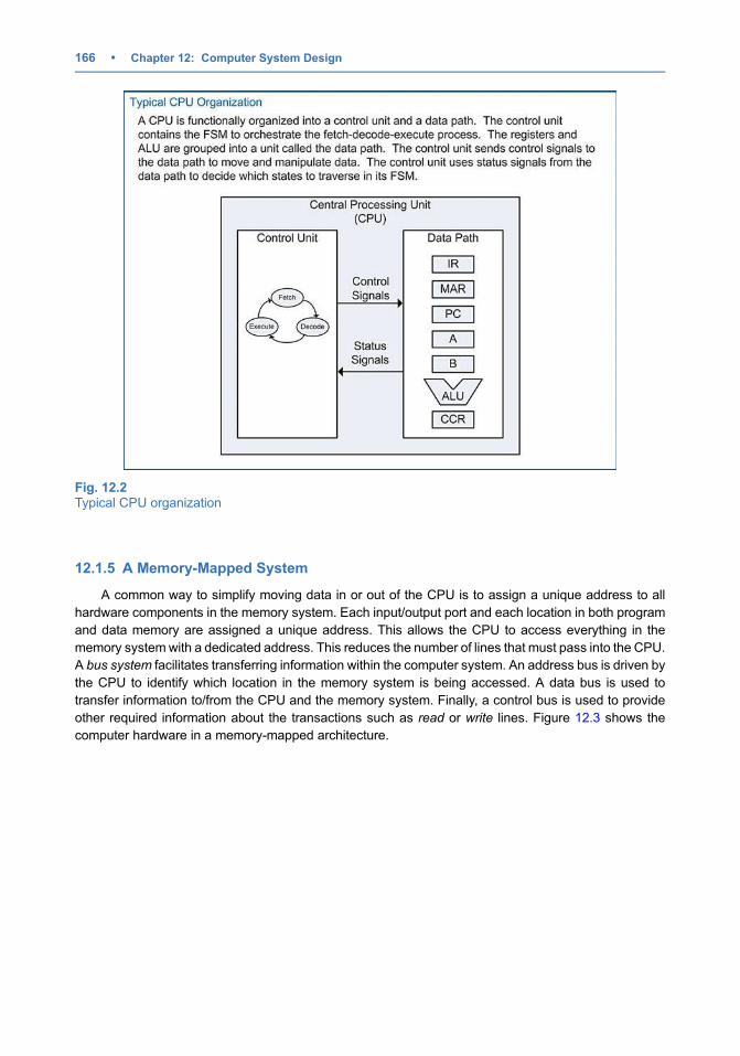
12.1.5 A Memory-Mapped System
A common way to simplify moving data in or out of the CPU is to assign a unique address to all
hardware components in the memory system. Each input/output port and each location in both program
and data memory are assigned a unique address. This allows the CPU to access everything in the
memory system with a dedicated address. This reduces the number of lines that must pass into the CPU.
A bus system facilitates transferring information within the computer system. An address bus is driven by
the CPU to identify which location in the memory system is being accessed. A data bus is used to
transfer information to/from the CPU and the memory system. Finally, a control bus is used to provide
other required information about the transactions such as read or write lines. Figure 12.3 shows the
computer hardware in a memory-mapped architecture.
Fig. 12.2Typical CPU organization
166 • Chapter 12: Computer System Design
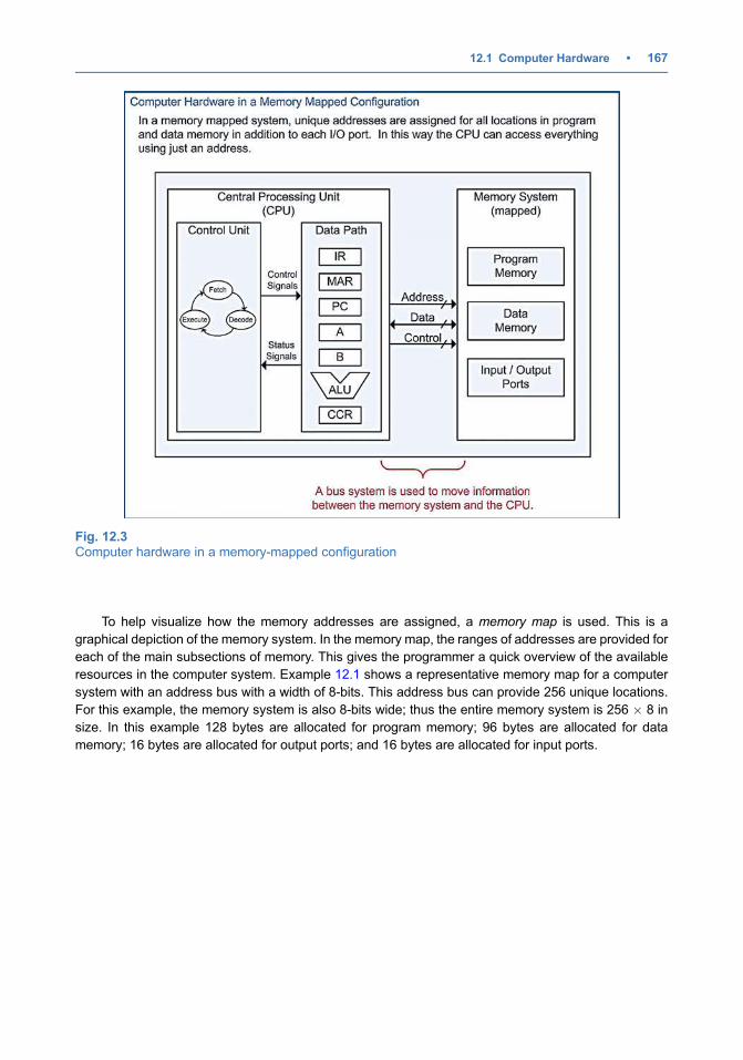
To help visualize how the memory addresses are assigned, a memory map is used. This is a
graphical depiction of the memory system. In the memory map, the ranges of addresses are provided for
each of the main subsections of memory. This gives the programmer a quick overview of the available
resources in the computer system. Example 12.1 shows a representative memory map for a computer
system with an address bus with a width of 8-bits. This address bus can provide 256 unique locations.
For this example, the memory system is also 8-bits wide; thus the entire memory system is 256 � 8 in
size. In this example 128 bytes are allocated for program memory; 96 bytes are allocated for data
memory; 16 bytes are allocated for output ports; and 16 bytes are allocated for input ports.
Fig. 12.3Computer hardware in a memory-mapped configuration
12.1 Computer Hardware • 167
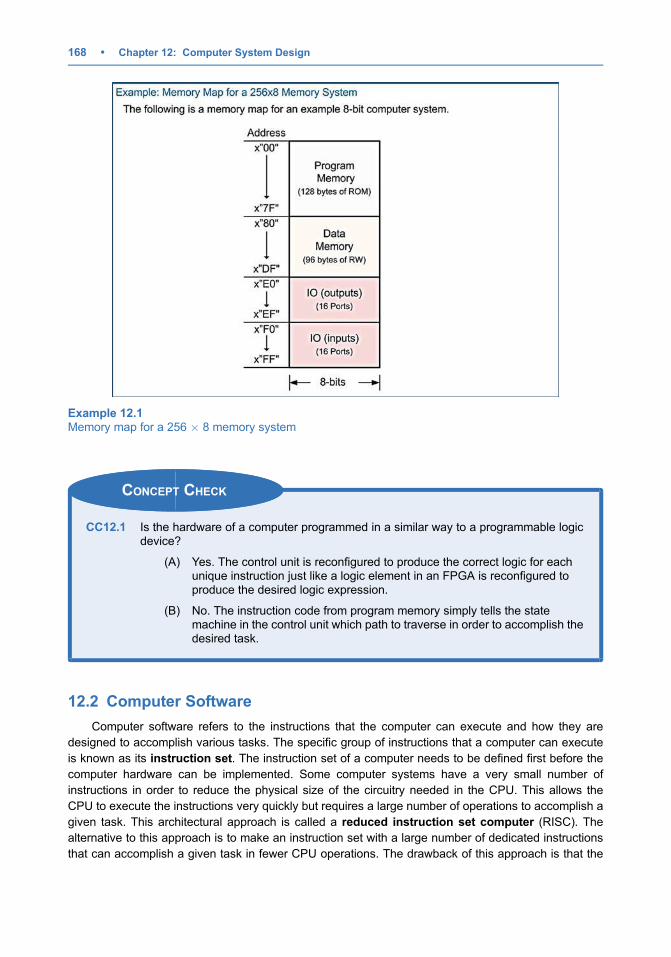
CONCEPT CHECK
CC12.1 Is the hardware of a computer programmed in a similar way to a programmable logicdevice?
(A) Yes. The control unit is reconfigured to produce the correct logic for eachunique instruction just like a logic element in an FPGA is reconfigured toproduce the desired logic expression.
(B) No. The instruction code from program memory simply tells the statemachine in the control unit which path to traverse in order to accomplish thedesired task.
12.2 Computer Software
Computer software refers to the instructions that the computer can execute and how they are
designed to accomplish various tasks. The specific group of instructions that a computer can execute
is known as its instruction set. The instruction set of a computer needs to be defined first before the
computer hardware can be implemented. Some computer systems have a very small number of
instructions in order to reduce the physical size of the circuitry needed in the CPU. This allows the
CPU to execute the instructions very quickly but requires a large number of operations to accomplish a
given task. This architectural approach is called a reduced instruction set computer (RISC). The
alternative to this approach is to make an instruction set with a large number of dedicated instructions
that can accomplish a given task in fewer CPU operations. The drawback of this approach is that the
Example 12.1Memory map for a 256 � 8 memory system
168 • Chapter 12: Computer System Design
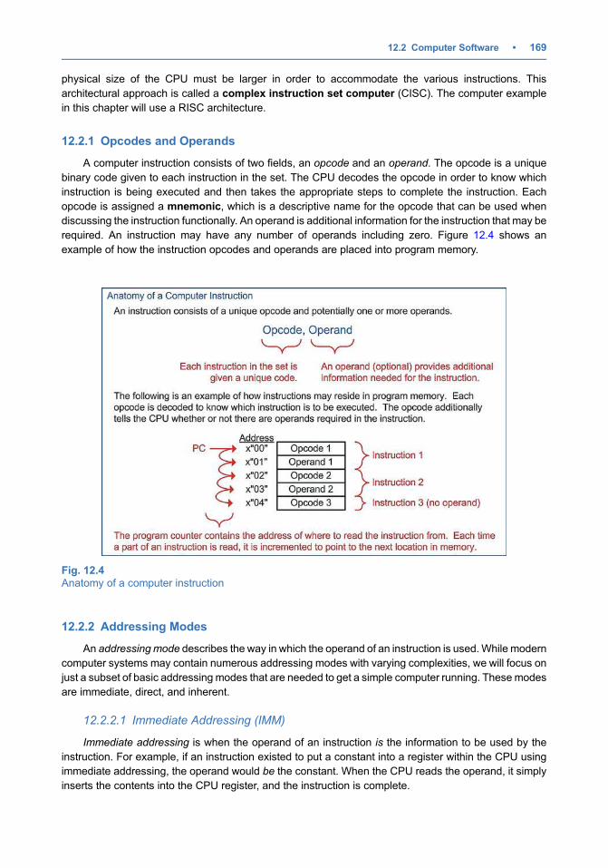
physical size of the CPU must be larger in order to accommodate the various instructions. This
architectural approach is called a complex instruction set computer (CISC). The computer example
in this chapter will use a RISC architecture.
12.2.1 Opcodes and Operands
A computer instruction consists of two fields, an opcode and an operand. The opcode is a unique
binary code given to each instruction in the set. The CPU decodes the opcode in order to know which
instruction is being executed and then takes the appropriate steps to complete the instruction. Each
opcode is assigned a mnemonic, which is a descriptive name for the opcode that can be used when
discussing the instruction functionally. An operand is additional information for the instruction that may be
required. An instruction may have any number of operands including zero. Figure 12.4 shows an
example of how the instruction opcodes and operands are placed into program memory.
12.2.2 Addressing Modes
An addressing mode describes the way in which the operand of an instruction is used. While modern
computer systems may contain numerous addressing modes with varying complexities, we will focus on
just a subset of basic addressing modes that are needed to get a simple computer running. These modes
are immediate, direct, and inherent.
12.2.2.1 Immediate Addressing (IMM)
Immediate addressing is when the operand of an instruction is the information to be used by the
instruction. For example, if an instruction existed to put a constant into a register within the CPU using
immediate addressing, the operand would be the constant. When the CPU reads the operand, it simply
inserts the contents into the CPU register, and the instruction is complete.
Fig. 12.4Anatomy of a computer instruction
12.2 Computer Software • 169
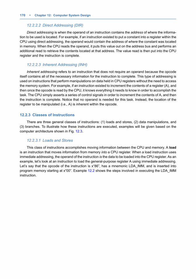
12.2.2.2 Direct Addressing (DIR)
Direct addressing is when the operand of an instruction contains the address of where the informa-
tion to be used is located. For example, if an instruction existed to put a constant into a register within the
CPU using direct addressing, the operand would contain the address of where the constant was located
in memory. When the CPU reads the operand, it puts this value out on the address bus and performs an
additional read to retrieve the contents located at that address. The value read is then put into the CPU
register and the instruction is complete.
12.2.2.3 Inherent Addressing (INH)
Inherent addressing refers to an instruction that does not require an operand because the opcode
itself contains all of the necessary information for the instruction to complete. This type of addressing is
used on instructions that performmanipulations on data held in CPU registers without the need to access
the memory system. For example, if an instruction existed to increment the contents of a register (A), and
then once the opcode is read by the CPU, it knows everything it needs to know in order to accomplish the
task. The CPU simply asserts a series of control signals in order to increment the contents of A, and then
the instruction is complete. Notice that no operand is needed for this task. Instead, the location of the
register to be manipulated (i.e., A) is inherent within the opcode.
12.2.3 Classes of Instructions
There are three general classes of instructions: (1) loads and stores, (2) data manipulations, and
(3) branches. To illustrate how these instructions are executed, examples will be given based on the
computer architecture shown in Fig. 12.3.
12.2.3.1 Loads and Stores
This class of instructions accomplishes moving information between the CPU and memory. A load
is an instruction that moves information from memory into a CPU register. When a load instruction uses
immediate addressing, the operand of the instruction is the data to be loaded into the CPU register. As an
example, let’s look at an instruction to load the general-purpose register A using immediate addressing.
Let’s say that the opcode of the instruction is x“86”, has a mnemonic LDA_IMM, and is inserted into
program memory starting at x“00”. Example 12.2 shows the steps involved in executing the LDA_IMM
instruction.
170 • Chapter 12: Computer System Design
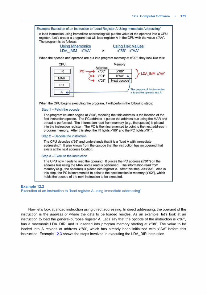
Now let’s look at a load instruction using direct addressing. In direct addressing, the operand of the
instruction is the address of where the data to be loaded resides. As an example, let’s look at an
instruction to load the general-purpose register A. Let’s say that the opcode of the instruction is x“87”,
has a mnemonic LDA_DIR, and is inserted into program memory starting at x“08”. The value to be
loaded into A resides at address x“80”, which has already been initialized with x“AA” before this
instruction. Example 12.3 shows the steps involved in executing the LDA_DIR instruction.
Example 12.2Execution of an instruction to “load register A using immediate addressing”
12.2 Computer Software • 171
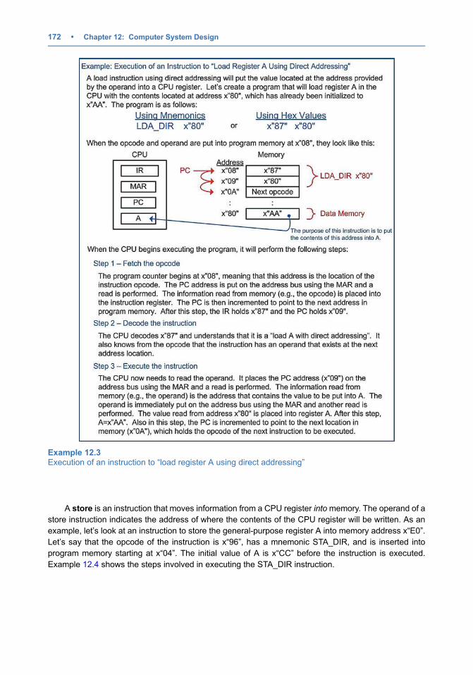
A store is an instruction that moves information from a CPU register intomemory. The operand of a
store instruction indicates the address of where the contents of the CPU register will be written. As an
example, let’s look at an instruction to store the general-purpose register A into memory address x“E0”.
Let’s say that the opcode of the instruction is x“96”, has a mnemonic STA_DIR, and is inserted into
program memory starting at x“04”. The initial value of A is x“CC” before the instruction is executed.
Example 12.4 shows the steps involved in executing the STA_DIR instruction.
Example 12.3Execution of an instruction to “load register A using direct addressing”
172 • Chapter 12: Computer System Design
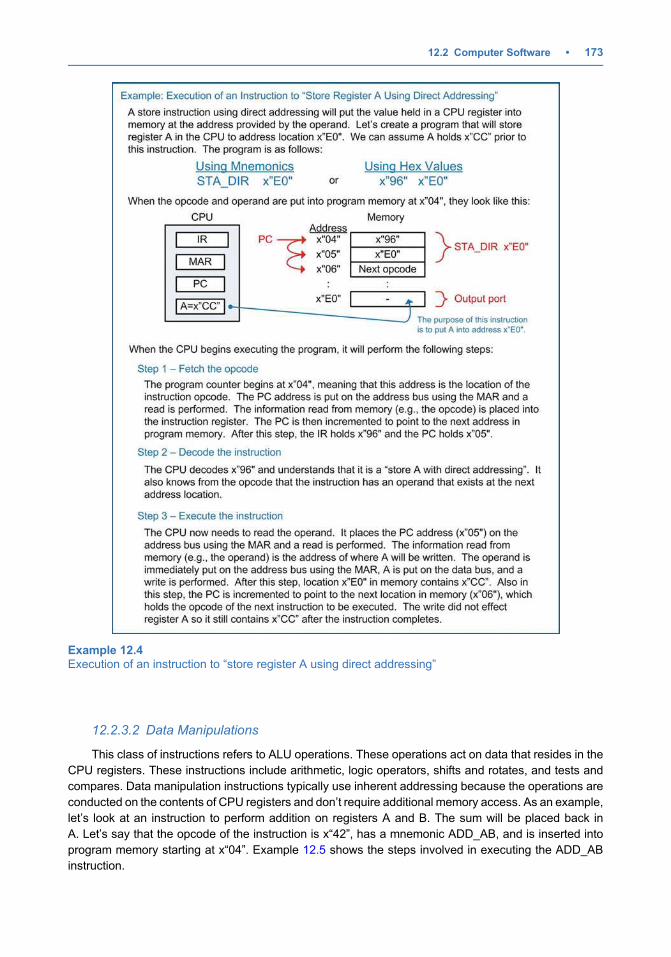
12.2.3.2 Data Manipulations
This class of instructions refers to ALU operations. These operations act on data that resides in the
CPU registers. These instructions include arithmetic, logic operators, shifts and rotates, and tests and
compares. Data manipulation instructions typically use inherent addressing because the operations are
conducted on the contents of CPU registers and don’t require additional memory access. As an example,
let’s look at an instruction to perform addition on registers A and B. The sum will be placed back in
A. Let’s say that the opcode of the instruction is x“42”, has a mnemonic ADD_AB, and is inserted into
program memory starting at x“04”. Example 12.5 shows the steps involved in executing the ADD_AB
instruction.
Example 12.4Execution of an instruction to “store register A using direct addressing”
12.2 Computer Software • 173
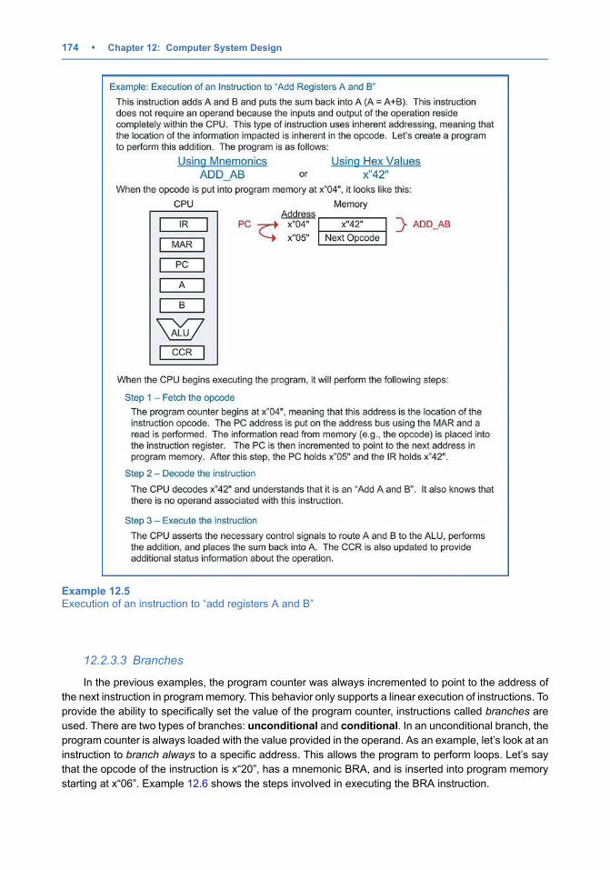
12.2.3.3 Branches
In the previous examples, the program counter was always incremented to point to the address of
the next instruction in programmemory. This behavior only supports a linear execution of instructions. To
provide the ability to specifically set the value of the program counter, instructions called branches are
used. There are two types of branches: unconditional and conditional. In an unconditional branch, the
program counter is always loaded with the value provided in the operand. As an example, let’s look at an
instruction to branch always to a specific address. This allows the program to perform loops. Let’s say
that the opcode of the instruction is x“20”, has a mnemonic BRA, and is inserted into program memory
starting at x“06”. Example 12.6 shows the steps involved in executing the BRA instruction.
Example 12.5Execution of an instruction to “add registers A and B”
174 • Chapter 12: Computer System Design
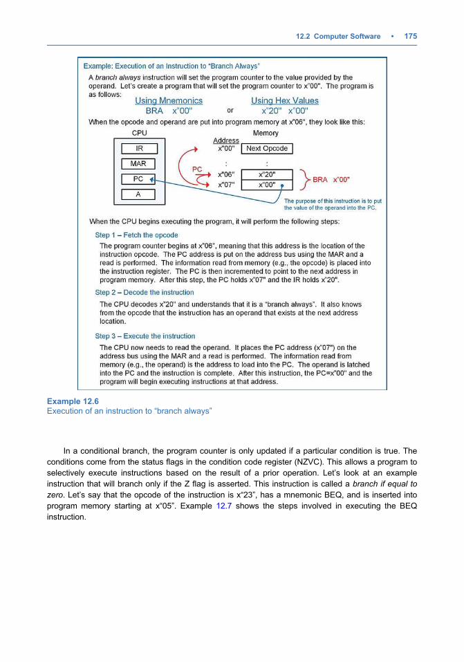
In a conditional branch, the program counter is only updated if a particular condition is true. The
conditions come from the status flags in the condition code register (NZVC). This allows a program to
selectively execute instructions based on the result of a prior operation. Let’s look at an example
instruction that will branch only if the Z flag is asserted. This instruction is called a branch if equal to
zero. Let’s say that the opcode of the instruction is x“23”, has a mnemonic BEQ, and is inserted into
program memory starting at x“05”. Example 12.7 shows the steps involved in executing the BEQ
instruction.
Example 12.6Execution of an instruction to “branch always”
12.2 Computer Software • 175
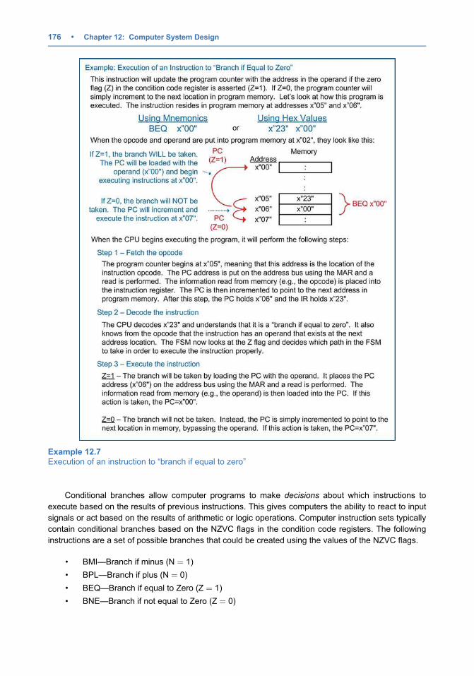
Conditional branches allow computer programs to make decisions about which instructions to
execute based on the results of previous instructions. This gives computers the ability to react to input
signals or act based on the results of arithmetic or logic operations. Computer instruction sets typically
contain conditional branches based on the NZVC flags in the condition code registers. The following
instructions are a set of possible branches that could be created using the values of the NZVC flags.
• BMI—Branch if minus (N ¼ 1)
• BPL—Branch if plus (N ¼ 0)
• BEQ—Branch if equal to Zero (Z ¼ 1)
• BNE—Branch if not equal to Zero (Z ¼ 0)
Example 12.7Execution of an instruction to “branch if equal to zero”
176 • Chapter 12: Computer System Design
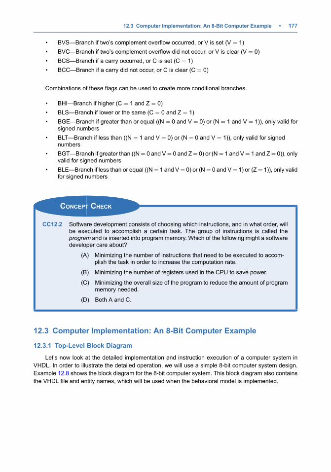
• BVS—Branch if two’s complement overflow occurred, or V is set (V ¼ 1)
• BVC—Branch if two’s complement overflow did not occur, or V is clear (V ¼ 0)
• BCS—Branch if a carry occurred, or C is set (C ¼ 1)
• BCC—Branch if a carry did not occur, or C is clear (C ¼ 0)
Combinations of these flags can be used to create more conditional branches.
• BHI—Branch if higher (C ¼ 1 and Z ¼ 0)
• BLS—Branch if lower or the same (C ¼ 0 and Z ¼ 1)
• BGE—Branch if greater than or equal ((N ¼ 0 and V ¼ 0) or (N ¼ 1 and V ¼ 1)), only valid forsigned numbers
• BLT—Branch if less than ((N ¼ 1 and V ¼ 0) or (N ¼ 0 and V ¼ 1)), only valid for signednumbers
• BGT—Branch if greater than ((N¼ 0 and V¼ 0 and Z¼ 0) or (N¼ 1 and V¼ 1 and Z¼ 0)), onlyvalid for signed numbers
• BLE—Branch if less than or equal ((N¼ 1 and V¼ 0) or (N¼ 0 and V¼ 1) or (Z¼ 1)), only validfor signed numbers
CONCEPT CHECK
CC12.2 Software development consists of choosing which instructions, and in what order, willbe executed to accomplish a certain task. The group of instructions is called theprogram and is inserted into program memory. Which of the following might a softwaredeveloper care about?
(A) Minimizing the number of instructions that need to be executed to accom-plish the task in order to increase the computation rate.
(B) Minimizing the number of registers used in the CPU to save power.
(C) Minimizing the overall size of the program to reduce the amount of programmemory needed.
(D) Both A and C.
12.3 Computer Implementation: An 8-Bit Computer Example
12.3.1 Top-Level Block Diagram
Let’s now look at the detailed implementation and instruction execution of a computer system in
VHDL. In order to illustrate the detailed operation, we will use a simple 8-bit computer system design.
Example 12.8 shows the block diagram for the 8-bit computer system. This block diagram also contains
the VHDL file and entity names, which will be used when the behavioral model is implemented.
12.3 Computer Implementation: An 8-Bit Computer Example • 177
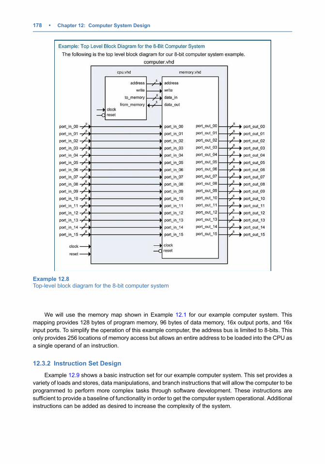
We will use the memory map shown in Example 12.1 for our example computer system. This
mapping provides 128 bytes of program memory, 96 bytes of data memory, 16x output ports, and 16x
input ports. To simplify the operation of this example computer, the address bus is limited to 8-bits. This
only provides 256 locations of memory access but allows an entire address to be loaded into the CPU as
a single operand of an instruction.
12.3.2 Instruction Set Design
Example 12.9 shows a basic instruction set for our example computer system. This set provides a
variety of loads and stores, data manipulations, and branch instructions that will allow the computer to be
programmed to perform more complex tasks through software development. These instructions are
sufficient to provide a baseline of functionality in order to get the computer system operational. Additional
instructions can be added as desired to increase the complexity of the system.
Example 12.8Top-level block diagram for the 8-bit computer system
178 • Chapter 12: Computer System Design
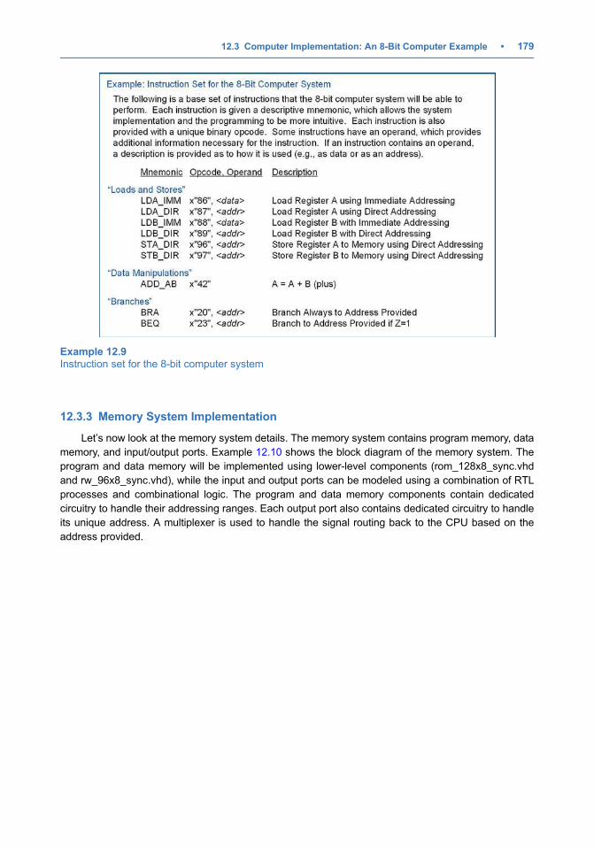
12.3.3 Memory System Implementation
Let’s now look at the memory system details. The memory system contains program memory, data
memory, and input/output ports. Example 12.10 shows the block diagram of the memory system. The
program and data memory will be implemented using lower-level components (rom_128x8_sync.vhd
and rw_96x8_sync.vhd), while the input and output ports can be modeled using a combination of RTL
processes and combinational logic. The program and data memory components contain dedicated
circuitry to handle their addressing ranges. Each output port also contains dedicated circuitry to handle
its unique address. A multiplexer is used to handle the signal routing back to the CPU based on the
address provided.
Example 12.9Instruction set for the 8-bit computer system
12.3 Computer Implementation: An 8-Bit Computer Example • 179
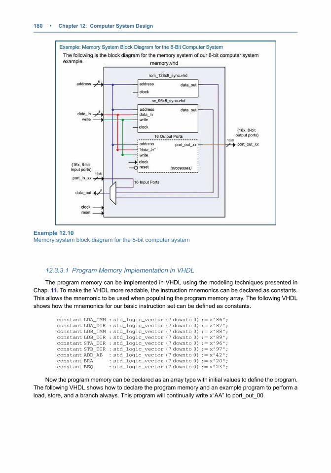
12.3.3.1 Program Memory Implementation in VHDL
The program memory can be implemented in VHDL using the modeling techniques presented in
Chap. 11. To make the VHDL more readable, the instruction mnemonics can be declared as constants.
This allows the mnemonic to be used when populating the program memory array. The following VHDL
shows how the mnemonics for our basic instruction set can be defined as constants.
constant LDA_IMM : std_logic_vector (7 downto 0) :¼ x"86";
constant LDA_DIR : std_logic_vector (7 downto 0) :¼ x"87";
constant LDB_IMM : std_logic_vector (7 downto 0) :¼ x"88";
constant LDB_DIR : std_logic_vector (7 downto 0) :¼ x"89";
constant STA_DIR : std_logic_vector (7 downto 0) :¼ x"96";
constant STB_DIR : std_logic_vector (7 downto 0) :¼ x"97";
constant ADD_AB : std_logic_vector (7 downto 0) :¼ x"42";
constant BRA : std_logic_vector (7 downto 0) :¼ x"20";
constant BEQ : std_logic_vector (7 downto 0) :¼ x"23";
Now the program memory can be declared as an array type with initial values to define the program.
The following VHDL shows how to declare the program memory and an example program to perform a
load, store, and a branch always. This program will continually write x“AA” to port_out_00.
Example 12.10Memory system block diagram for the 8-bit computer system
180 • Chapter 12: Computer System Design
type rom_type is array (0 to 127) of std_logic_vector(7 downto 0);
constant ROM : rom_type :¼ (0 ¼> LDA_IMM,
1 ¼> x"AA",
2 ¼> STA_DIR,
3 ¼> x"E0",
4 ¼> BRA,
5 ¼> x"00",
others ¼> x"00");
The address mapping for the program memory is handled in two ways. First, notice that the array
type defined above uses indices from 0 to 127. This provides the appropriate addresses for each location
in the memory. The second step is to create an internal enable line that will only allow assignments from
ROM to data_out when a valid address is entered. Consider the following VHDL to create an internal
enable (EN) that will only be asserted when the address falls within the valid program memory range of
0 to 127.
enable : process (address)
begin
if ((to_integer(unsigned(address)) >¼ 0) and
(to_integer(unsigned(address)) <¼ 127)) then
EN <¼ ’1’;
else
EN <¼ ’0’;
end if;
end process;
If this enable signal is not created, the simulation and synthesis will fail because data_out
assignments will be attempted for addresses outside of the defined range of the ROM array. This enable
line can now be used in the behavioral model for the ROM process as follows:
memory : process (clock)
begin
if (clock’event and clock¼’1’) then
if (EN¼’1’) then
data_out <¼ ROM(to_integer(unsigned(address)));
end if;
end if;
end process;
12.3.3.2 Data Memory Implementation in VHDL
The data memory is created using a similar strategy as the program memory. An array signal is
declared with an address range corresponding to the memory map for the computer system (i.e., 128 to
223). An internal enable is again created that will prevent data_out assignments for addresses outside of
this valid range. The following is the VHDL to declare the R/W memory array:
type rw_type is array (128 to 223) of std_logic_vector(7 downto 0);
signal RW : rw_type;
12.3 Computer Implementation: An 8-Bit Computer Example • 181
The following is the VHDL to model the local enable and signal assignments for the R/W memory:
enable : process (address)
begin
if ( (to_integer(unsigned(address)) >¼ 128) and
(to_integer(unsigned(address)) <¼ 223)) then
EN <¼ ’1’;
else
EN <¼ ’0’;
end if;
end process;
memory : process (clock)
begin
if (clock’event and clock¼’1’) then
if (EN¼’1’ and write¼’1’) then
RW(to_integer(unsigned(address))) <¼ data_in;
elsif (EN¼’1’ and write¼’0’) then
data_out <¼ RW(to_integer(unsigned(address)));
end if;
end if;
end process;
12.3.3.3 Implementation of Output Ports in VHDL
Each output port in the computer system is assigned a unique address. Each output port also
contains storage capability. This allows the CPU to update an output port by writing to its specific
address. Once the CPU is done storing to the output port address and moves to the next instruction in
the program, the output port holds its information until it is written to again. This behavior can be modeled
using an RTL process that uses the address bus and the write signal to create a synchronous enable
condition. Each port is modeled with its own process. The following VHDL shows how the output ports at
x“E0” and x“E1” are modeled using address specific processes.
-- port_out_00 description : ADDRESS x"E0"
U3 : process (clock, reset)
begin
if (reset ¼ ’0’) then
port_out_00 <¼ x"00";
elsif (clock’event and clock¼’1’) then
if (address ¼ x"E0" and write ¼ ’1’) then
port_out_00 <¼ data_in;
end if;
end if;
end process;
-- port_out_01 description : ADDRESS x"E1"
U4 : process (clock, reset)
begin
if (reset ¼ ’0’) then
port_out_01 <¼ x"00";
elsif (clock’event and clock¼’1’) then
if (address ¼ x"E1" and write ¼ ’1’) then
port_out_01 <¼ data_in;
end if;
end if;
end process;
:
“the rest of the output port models go here. . .”
:
182 • Chapter 12: Computer System Design
12.3.3.4 Implementation of Input Ports in VHDL
The input ports do not contain storage but do require a mechanism to selectively route their
information to the data_out port of the memory system. This is accomplished using the multiplexer
shown in Example 12.10. The only functionality that is required for the input ports is connecting their
ports to the multiplexer.
12.3.3.5 Memory data_out Bus Implementation in VHDL
Now that all of the memory functionality has been designed, the final step is to implement the
multiplexer that handles routing the appropriate information to the CPU on the data_out bus based on the
incoming address. The following VHDL provides a model for this behavior. Recall that a multiplexer is
combinational logic, so if the behavior is to be modeled using a process, all inputs must be listed in the
sensitivity list. These inputs include the outputs from the program and data memory in addition to all of
the input ports. The sensitivity list must also include the address bus as it acts as the select input to the
multiplexer. Within the process, an if/then statement is used to determine which sub-system drives
data_out. Program memory will drive data_out when the incoming address is in the range of 0 to
127 (x“00” to x“7F”). Data memory will drive data_out when the address is in the range of 128 to
223 (x“80” to x“DF”). An input port will drive data_out when the address is in the range of 240 to
255 (x“F0” to x“FF”). Each input port has a unique address, so the specific addresses are listed as
elsif clauses.
MUX1 : process (address, rom_data_out, rw_data_out,
port_in_00, port_in_01, port_in_02, port_in_03,
port_in_04, port_in_05, port_in_06, port_in_07,
port_in_08, port_in_09, port_in_10, port_in_11,
port_in_12, port_in_13, port_in_14, port_in_15)
begin
if ( (to_integer(unsigned(address)) >¼ 0) and
(to_integer(unsigned(address)) <¼ 127)) then
data_out <¼ rom_data_out;
elsif ( (to_integer(unsigned(address)) >¼ 128) and
(to_integer(unsigned(address)) <¼ 223)) then
data_out <¼ rw_data_out;
elsif (address ¼ x"F0") then data_out <¼ port_in_00;
elsif (address ¼ x"F1") then data_out <¼ port_in_01;
elsif (address ¼ x"F2") then data_out <¼ port_in_02;
elsif (address ¼ x"F3") then data_out <¼ port_in_03;
elsif (address ¼ x"F4") then data_out <¼ port_in_04;
elsif (address ¼ x"F5") then data_out <¼ port_in_05;
elsif (address ¼ x"F6") then data_out <¼ port_in_06;
elsif (address ¼ x"F7") then data_out <¼ port_in_07;
elsif (address ¼ x"F8") then data_out <¼ port_in_08;
elsif (address ¼ x"F9") then data_out <¼ port_in_09;
elsif (address ¼ x"FA") then data_out <¼ port_in_10;
elsif (address ¼ x"FB") then data_out <¼ port_in_11;
elsif (address ¼ x"FC") then data_out <¼ port_in_12;
elsif (address ¼ x"FD") then data_out <¼ port_in_13;
elsif (address ¼ x"FE") then data_out <¼ port_in_14;
elsif (address ¼ x"FF") then data_out <¼ port_in_15;
else data_out <¼ x"00";
end if;
end process;
12.3 Computer Implementation: An 8-Bit Computer Example • 183
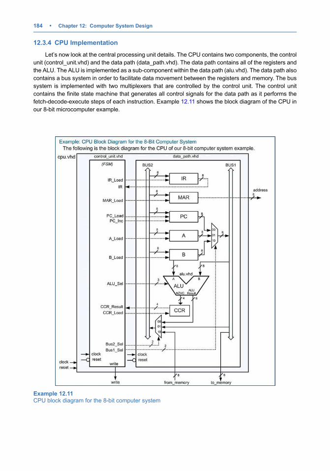
12.3.4 CPU Implementation
Let’s now look at the central processing unit details. The CPU contains two components, the control
unit (control_unit.vhd) and the data path (data_path.vhd). The data path contains all of the registers and
the ALU. The ALU is implemented as a sub-component within the data path (alu.vhd). The data path also
contains a bus system in order to facilitate data movement between the registers and memory. The bus
system is implemented with two multiplexers that are controlled by the control unit. The control unit
contains the finite state machine that generates all control signals for the data path as it performs the
fetch-decode-execute steps of each instruction. Example 12.11 shows the block diagram of the CPU in
our 8-bit microcomputer example.
Example 12.11CPU block diagram for the 8-bit computer system
184 • Chapter 12: Computer System Design
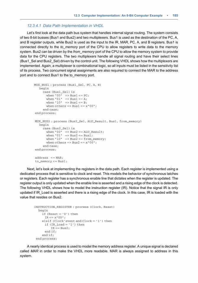
12.3.4.1 Data Path Implementation in VHDL
Let’s first look at the data path bus system that handles internal signal routing. The system consists
of two 8-bit busses (Bus1 and Bus2) and two multiplexers. Bus1 is used as the destination of the PC, A,
and B register outputs, while Bus2 is used as the input to the IR, MAR, PC, A, and B registers. Bus1 is
connected directly to the to_memory port of the CPU to allow registers to write data to the memory
system. Bus2 can be driven by the from_memory port of the CPU to allow the memory system to provide
data for the CPU registers. The two multiplexers handle all signal routing and have their select lines
(Bus1_Sel and Bus2_Sel) driven by the control unit. The following VHDL shows how the multiplexers are
implemented. Again, a multiplexer is combinational logic, so all inputs must be listed in the sensitivity list
of its process. Two concurrent signal assignments are also required to connect the MAR to the address
port and to connect Bus1 to the to_memory port.
MUX_BUS1 : process (Bus1_Sel, PC, A, B)
begin
case (Bus1_Sel) is
when "00" ¼> Bus1 <¼ PC;
when "01" ¼> Bus1 <¼ A;
when "10" ¼> Bus1 <¼ B;
when others ¼> Bus1 <¼ x"00";
end case;
end process;
MUX_BUS2 : process (Bus2_Sel, ALU_Result, Bus1, from_memory)
begin
case (Bus2_Sel) is
when "00" ¼> Bus2 <¼ ALU_Result;
when "01" ¼> Bus2 <¼ Bus1;
when "10" ¼> Bus2 <¼ from_memory;
when others ¼> Bus2 <¼ x"00";
end case;
end process;
address <¼ MAR;
to_memory <¼ Bus1;
Next, let’s look at implementing the registers in the data path. Each register is implemented using a
dedicated process that is sensitive to clock and reset. This models the behavior of synchronous latches
or registers. Each register has a synchronous enable line that dictates when the register is updated. The
register output is only updated when the enable line is asserted and a rising edge of the clock is detected.
The following VHDL shows how to model the instruction register (IR). Notice that the signal IR is only
updated if IR_Load is asserted and there is a rising edge of the clock. In this case, IR is loaded with the
value that resides on Bus2.
INSTRUCTION_REGISTER : process (Clock, Reset)
begin
if (Reset ¼ ’0’) then
IR <¼ x"00";
elsif (Clock’event and Clock ¼ ’1’) then
if (IR_Load ¼ ’1’) then
IR <¼ Bus2;
end if;
end if;
end process;
A nearly identical process is used to model the memory address register. A unique signal is declared
called MAR in order to make the VHDL more readable. MAR is always assigned to address in this
system.
12.3 Computer Implementation: An 8-Bit Computer Example • 185
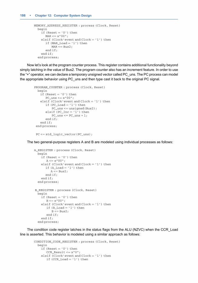
MEMORY_ADDRESS_REGISTER : process (Clock, Reset)
begin
if (Reset ¼ ’0’) then
MAR <¼ x"00";
elsif (Clock’event and Clock ¼ ’1’) then
if (MAR_Load ¼ ’1’) then
MAR <¼ Bus2;
end if;
end if;
end process;
Now let’s look at the program counter process. This register contains additional functionality beyond
simply latching in the value of Bus2. The program counter also has an increment feature. In order to use
the “+” operator, we can declare a temporary unsigned vector called PC_uns. The PC process can model
the appropriate behavior using PC_uns and then type cast it back to the original PC signal.
PROGRAM_COUNTER : process (Clock, Reset)
begin
if (Reset ¼ ’0’) then
PC_uns <¼ x"00";
elsif (Clock’event and Clock ¼ ’1’) then
if (PC_Load ¼ ’1’) then
PC_uns <¼ unsigned(Bus2);
elsif (PC_Inc ¼ ’1’) then
PC_uns <¼ PC_uns + 1;
end if;
end if;
end process;
PC <¼ std_logic_vector(PC_uns);
The two general-purpose registers A and B are modeled using individual processes as follows:
A_REGISTER : process (Clock, Reset)
begin
if (Reset ¼ ’0’) then
A <¼ x"00";
elsif (Clock’event and Clock ¼ ’1’) then
if (A_Load ¼ ’1’) then
A <¼ Bus2;
end if;
end if;
end process;
B_REGISTER : process (Clock, Reset)
begin
if (Reset ¼ ’0’) then
B <¼ x"00";
elsif (Clock’event and Clock ¼ ’1’) then
if (B_Load ¼ ’1’) then
B <¼ Bus2;
end if;
end if;
end process;
The condition code register latches in the status flags from the ALU (NZVC) when the CCR_Load
line is asserted. This behavior is modeled using a similar approach as follows:
CONDITION_CODE_REGISTER : process (Clock, Reset)
begin
if (Reset ¼ ’0’) then
CCR_Result <¼ x"0";
elsif (Clock’event and Clock ¼ ’1’) then
if (CCR_Load ¼ ’1’) then
186 • Chapter 12: Computer System Design
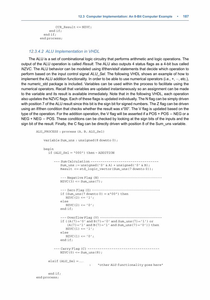
CCR_Result <¼ NZVC;
end if;
end if;
end process;
12.3.4.2 ALU Implementation in VHDL
The ALU is a set of combinational logic circuitry that performs arithmetic and logic operations. The
output of the ALU operation is called Result. The ALU also outputs 4 status flags as a 4-bit bus called
NZVC. The ALU behavior can be modeled using if/then/elsif statements that decide which operation to
perform based on the input control signal ALU_Sel. The following VHDL shows an example of how to
implement the ALU addition functionality. In order to be able to use numerical operators (i.e., +, �, etc.),
the numeric_std package is included. Variables can be used within the process to facilitate using the
numerical operators. Recall that variables are updated instantaneously so an assignment can be made
to the variable and its result is available immediately. Note that in the following VHDL, each operation
also updates the NZVC flags. Each of these flags is updated individually. The N flag can be simply driven
with position 7 of the ALU result since this bit is the sign bit for signed numbers. The Z flag can be driven
using an if/then condition that checks whether the result was x“00”. The V flag is updated based on the
type of the operation. For the addition operation, the V flag will be asserted if a POS + POS ¼ NEG or a
NEG + NEG ¼ POS. These conditions can be checked by looking at the sign bits of the inputs and the
sign bit of the result. Finally, the C flag can be directly driven with position 8 of the Sum_uns variable.
ALU_PROCESS : process (A, B, ALU_Sel)
variable Sum_uns : unsigned(8 downto 0);
begin
if (ALU_Sel ¼ "000") then – ADDITION
--- Sum Calculation ---------------------------------–
Sum_uns :¼ unsigned(’0’ & A) + unsigned(’0’ & B);
Result <¼ std_logic_vector(Sum_uns(7 downto 0));
--- Negative Flag (N) -------------------------------
NZVC(3) <¼ Sum_uns(7);
--- Zero Flag (Z) ---------------------------------–
if (Sum_uns(7 downto 0) ¼ x"00") then
NZVC(2) <¼ ’1’;
else
NZVC(2) <¼ ’0’;
end if;
--- Overflow Flag (V) -------------------------------
if ((A(7)¼’0’ and B(7)¼’0’ and Sum_uns(7)¼’1’) or
(A(7)¼’1’ and B(7)¼’1’ and Sum_uns(7)¼’0’)) then
NZVC(1) <¼ ’1’;
else
NZVC(1) <¼ ’0’;
end if;
--- Carry Flag (C) ------------------------------------
NZVC(0) <¼ Sum_uns(8);
elsif (ALU_Sel ¼ . . .
: “other ALU functionality goes here”
end if;
end process;
12.3 Computer Implementation: An 8-Bit Computer Example • 187
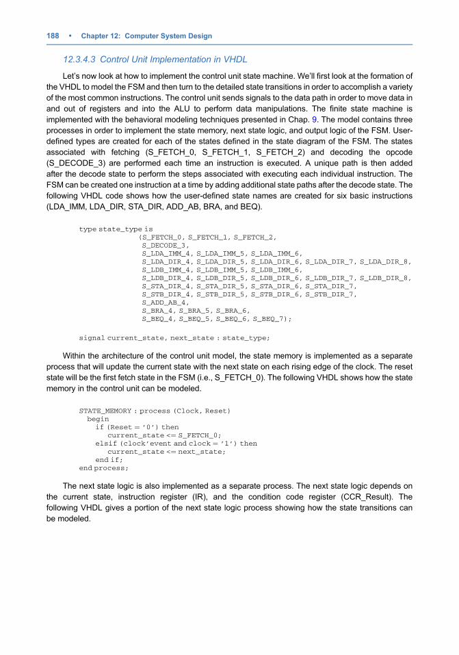
12.3.4.3 Control Unit Implementation in VHDL
Let’s now look at how to implement the control unit state machine. We’ll first look at the formation of
the VHDL to model the FSM and then turn to the detailed state transitions in order to accomplish a variety
of the most common instructions. The control unit sends signals to the data path in order to move data in
and out of registers and into the ALU to perform data manipulations. The finite state machine is
implemented with the behavioral modeling techniques presented in Chap. 9. The model contains three
processes in order to implement the state memory, next state logic, and output logic of the FSM. User-
defined types are created for each of the states defined in the state diagram of the FSM. The states
associated with fetching (S_FETCH_0, S_FETCH_1, S_FETCH_2) and decoding the opcode
(S_DECODE_3) are performed each time an instruction is executed. A unique path is then added
after the decode state to perform the steps associated with executing each individual instruction. The
FSM can be created one instruction at a time by adding additional state paths after the decode state. The
following VHDL code shows how the user-defined state names are created for six basic instructions
(LDA_IMM, LDA_DIR, STA_DIR, ADD_AB, BRA, and BEQ).
type state_type is
(S_FETCH_0, S_FETCH_1, S_FETCH_2,
S_DECODE_3,
S_LDA_IMM_4, S_LDA_IMM_5, S_LDA_IMM_6,
S_LDA_DIR_4, S_LDA_DIR_5, S_LDA_DIR_6, S_LDA_DIR_7, S_LDA_DIR_8,
S_LDB_IMM_4, S_LDB_IMM_5, S_LDB_IMM_6,
S_LDB_DIR_4, S_LDB_DIR_5, S_LDB_DIR_6, S_LDB_DIR_7, S_LDB_DIR_8,
S_STA_DIR_4, S_STA_DIR_5, S_STA_DIR_6, S_STA_DIR_7,
S_STB_DIR_4, S_STB_DIR_5, S_STB_DIR_6, S_STB_DIR_7,
S_ADD_AB_4,
S_BRA_4, S_BRA_5, S_BRA_6,
S_BEQ_4, S_BEQ_5, S_BEQ_6, S_BEQ_7);
signal current_state, next_state : state_type;
Within the architecture of the control unit model, the state memory is implemented as a separate
process that will update the current state with the next state on each rising edge of the clock. The reset
state will be the first fetch state in the FSM (i.e., S_FETCH_0). The following VHDL shows how the state
memory in the control unit can be modeled.
STATE_MEMORY : process (Clock, Reset)
begin
if (Reset ¼ ’0’) then
current_state <¼ S_FETCH_0;
elsif (clock’event and clock ¼ ’1’) then
current_state <¼ next_state;
end if;
end process;
The next state logic is also implemented as a separate process. The next state logic depends on
the current state, instruction register (IR), and the condition code register (CCR_Result). The
following VHDL gives a portion of the next state logic process showing how the state transitions can
be modeled.
188 • Chapter 12: Computer System Design
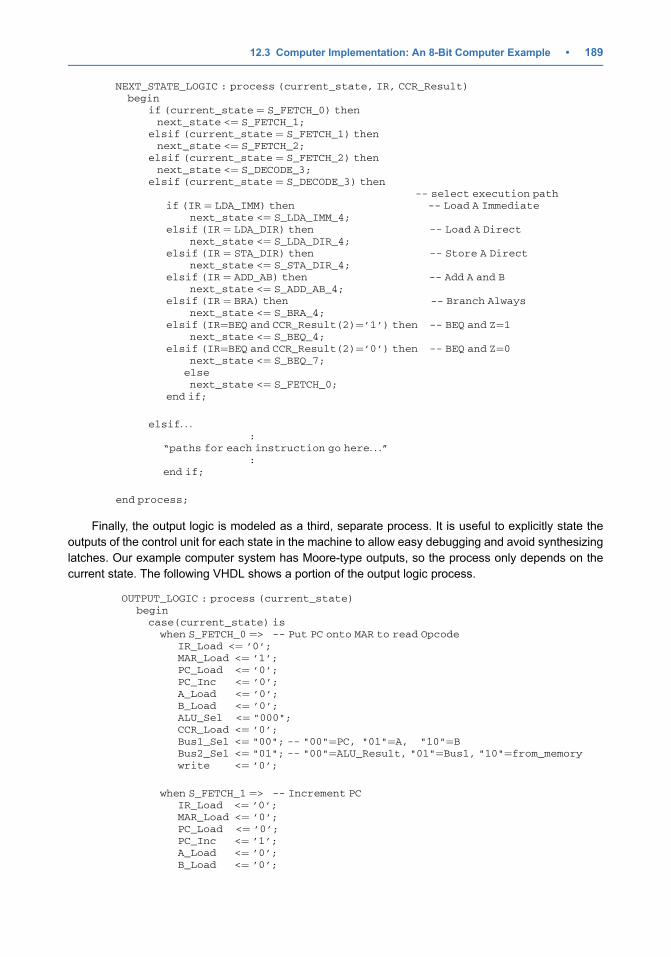
NEXT_STATE_LOGIC : process (current_state, IR, CCR_Result)
begin
if (current_state ¼ S_FETCH_0) then
next_state <¼ S_FETCH_1;
elsif (current_state ¼ S_FETCH_1) then
next_state <¼ S_FETCH_2;
elsif (current_state ¼ S_FETCH_2) then
next_state <¼ S_DECODE_3;
elsif (current_state ¼ S_DECODE_3) then
-- select execution path
if (IR ¼ LDA_IMM) then -- Load A Immediate
next_state <¼ S_LDA_IMM_4;
elsif (IR ¼ LDA_DIR) then -- Load A Direct
next_state <¼ S_LDA_DIR_4;
elsif (IR ¼ STA_DIR) then -- Store A Direct
next_state <¼ S_STA_DIR_4;
elsif (IR ¼ ADD_AB) then -- Add A and B
next_state <¼ S_ADD_AB_4;
elsif (IR ¼ BRA) then -- Branch Always
next_state <¼ S_BRA_4;
elsif (IR¼BEQ and CCR_Result(2)¼’1’) then -- BEQ and Z¼1
next_state <¼ S_BEQ_4;
elsif (IR¼BEQ and CCR_Result(2)¼’0’) then -- BEQ and Z¼0
next_state <¼ S_BEQ_7;
else
next_state <¼ S_FETCH_0;
end if;
elsif. . .
:
“paths for each instruction go here. . .”
:
end if;
end process;
Finally, the output logic is modeled as a third, separate process. It is useful to explicitly state the
outputs of the control unit for each state in the machine to allow easy debugging and avoid synthesizing
latches. Our example computer system has Moore-type outputs, so the process only depends on the
current state. The following VHDL shows a portion of the output logic process.
OUTPUT_LOGIC : process (current_state)
begin
case(current_state) is
when S_FETCH_0 ¼> -- Put PC onto MAR to read Opcode
IR_Load <¼ ’0’;
MAR_Load <¼ ’1’;
PC_Load <¼ ’0’;
PC_Inc <¼ ’0’;
A_Load <¼ ’0’;
B_Load <¼ ’0’;
ALU_Sel <¼ "000";
CCR_Load <¼ ’0’;
Bus1_Sel <¼ "00"; -- "00"¼PC, "01"¼A, "10"¼B
Bus2_Sel <¼ "01"; -- "00"¼ALU_Result, "01"¼Bus1, "10"¼from_memory
write <¼ ’0’;
when S_FETCH_1 ¼> -- Increment PC
IR_Load <¼ ’0’;
MAR_Load <¼ ’0’;
PC_Load <¼ ’0’;
PC_Inc <¼ ’1’;
A_Load <¼ ’0’;
B_Load <¼ ’0’;
12.3 Computer Implementation: An 8-Bit Computer Example • 189
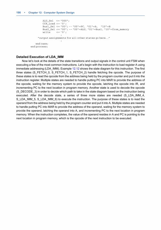
ALU_Sel <¼ "000";
CCR_Load <¼ ’0’;
Bus1_Sel <¼ "00"; -- "00"¼PC, "01"¼A, "10"¼B
Bus2_Sel <¼ "00"; -- "00"¼ALU, "01"¼Bus1, "10"¼from_memory
write <¼ ’0’;
:
“output assignments for all other states go here. . .”
:
end case;
end process;
Detailed Execution of LDA_IMM
Now let’s look at the details of the state transitions and output signals in the control unit FSM when
executing a few of the most common instructions. Let’s begin with the instruction to load register A using
immediate addressing (LDA_IMM). Example 12.12 shows the state diagram for this instruction. The first
three states (S_FETCH_0, S_FETCH_1, S_FETCH_2) handle fetching the opcode. The purpose of
these states is to read the opcode from the address being held by the program counter and put it into the
instruction register. Multiple states are needed to handle putting PC into MAR to provide the address of
the opcode, waiting for the memory system to provide the opcode, latching the opcode into IR, and
incrementing PC to the next location in program memory. Another state is used to decode the opcode
(S_DECODE_3) in order to decide which path to take in the state diagram based on the instruction being
executed. After the decode state, a series of three more states are needed (S_LDA_IMM_4,
S_LDA_IMM_5, S_LDA_IMM_6) to execute the instruction. The purpose of these states is to read the
operand from the address being held by the program counter and put it into A. Multiple states are needed
to handle putting PC into MAR to provide the address of the operand, waiting for the memory system to
provide the operand, latching the operand into A, and incrementing PC to the next location in program
memory. When the instruction completes, the value of the operand resides in A and PC is pointing to the
next location in program memory, which is the opcode of the next instruction to be executed.
190 • Chapter 12: Computer System Design
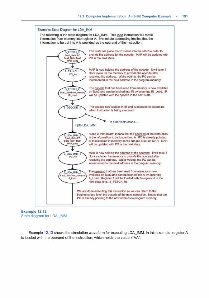
Example 12.13 shows the simulation waveform for executing LDA_IMM. In this example, register A
is loaded with the operand of the instruction, which holds the value x“AA”.
Example 12.12State diagram for LDA_IMM
12.3 Computer Implementation: An 8-Bit Computer Example • 191
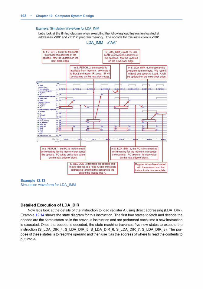
Detailed Execution of LDA_DIR
Now let’s look at the details of the instruction to load register A using direct addressing (LDA_DIR).
Example 12.14 shows the state diagram for this instruction. The first four states to fetch and decode the
opcode are the same states as in the previous instruction and are performed each time a new instruction
is executed. Once the opcode is decoded, the state machine traverses five new states to execute the
instruction (S_LDA_DIR_4, S_LDA_DIR_5, S_LDA_DIR_6, S_LDA_DIR_7, S_LDA_DIR_8). The pur-
pose of these states is to read the operand and then use it as the address of where to read the contents to
put into A.
Example 12.13Simulation waveform for LDA_IMM
192 • Chapter 12: Computer System Design
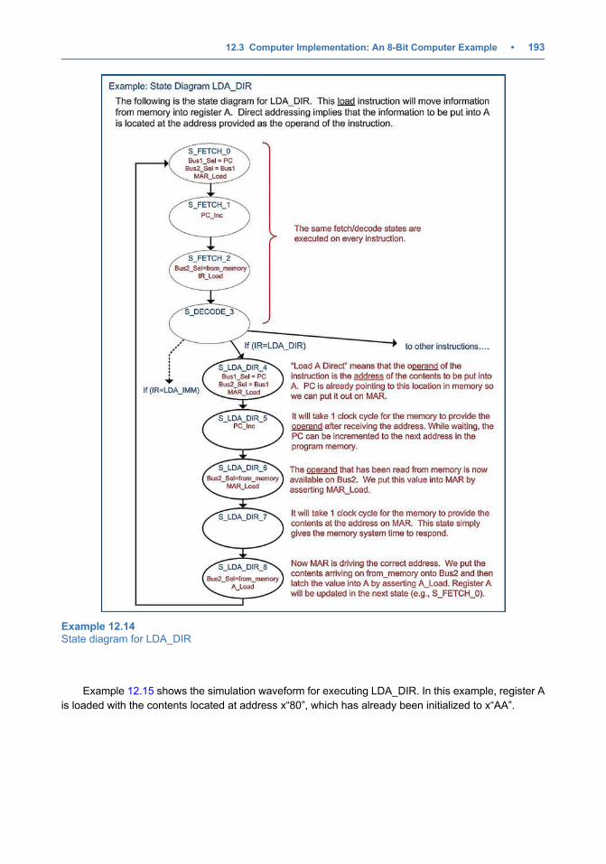
Example 12.15 shows the simulation waveform for executing LDA_DIR. In this example, register A
is loaded with the contents located at address x“80”, which has already been initialized to x“AA”.
Example 12.14State diagram for LDA_DIR
12.3 Computer Implementation: An 8-Bit Computer Example • 193
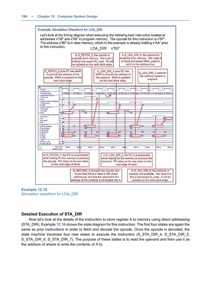
Detailed Execution of STA_DIR
Now let’s look at the details of the instruction to store register A to memory using direct addressing
(STA_DIR). Example 12.16 shows the state diagram for this instruction. The first four states are again the
same as prior instructions in order to fetch and decode the opcode. Once the opcode is decoded, the
state machine traverses four new states to execute the instruction (S_STA_DIR_4, S_STA_DIR_5,
S_STA_DIR_6, S_STA_DIR_7). The purpose of these states is to read the operand and then use it as
the address of where to write the contents of A to.
Example 12.15Simulation waveform for LDA_DIR
194 • Chapter 12: Computer System Design
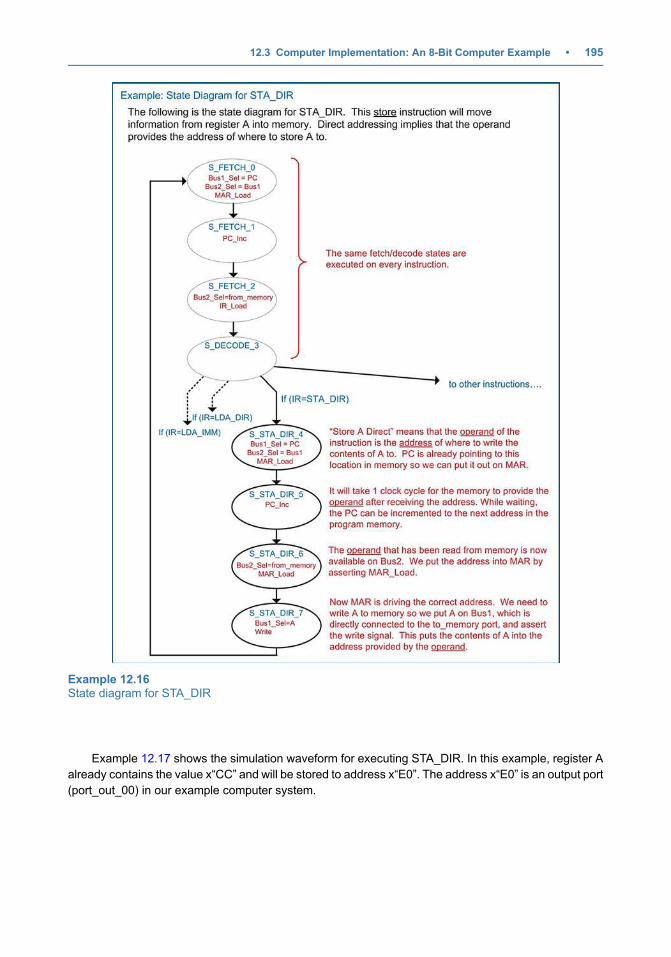
Example 12.17 shows the simulation waveform for executing STA_DIR. In this example, register A
already contains the value x“CC” and will be stored to address x“E0”. The address x“E0” is an output port
(port_out_00) in our example computer system.
Example 12.16State diagram for STA_DIR
12.3 Computer Implementation: An 8-Bit Computer Example • 195
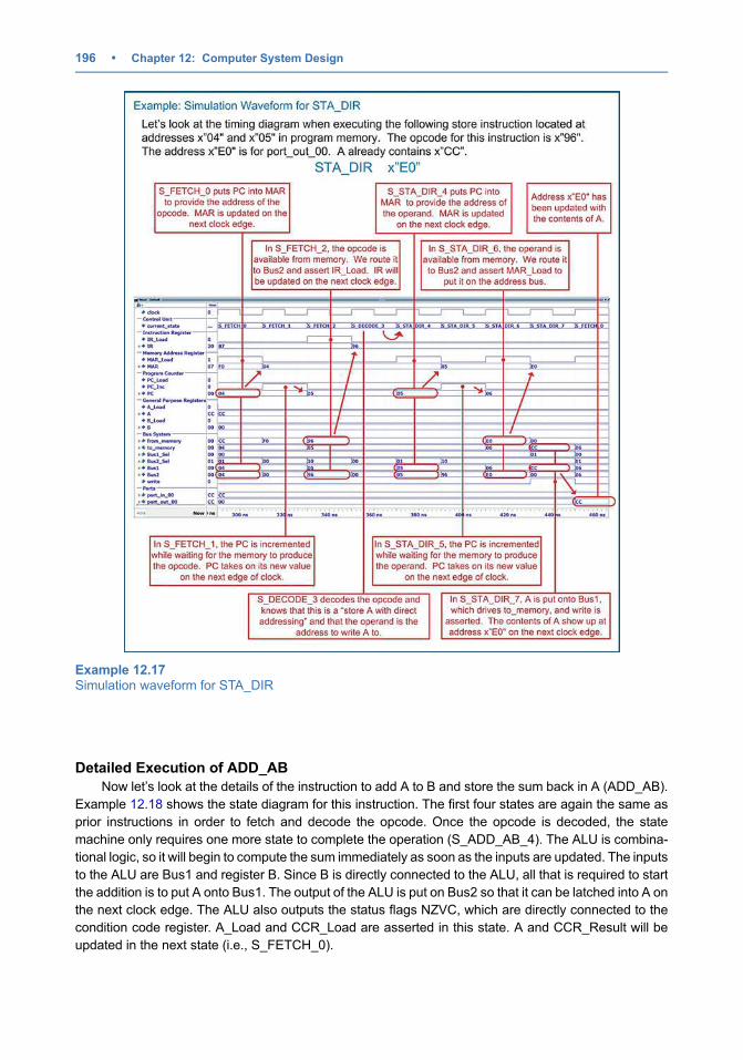
Detailed Execution of ADD_AB
Now let’s look at the details of the instruction to add A to B and store the sum back in A (ADD_AB).
Example 12.18 shows the state diagram for this instruction. The first four states are again the same as
prior instructions in order to fetch and decode the opcode. Once the opcode is decoded, the state
machine only requires one more state to complete the operation (S_ADD_AB_4). The ALU is combina-
tional logic, so it will begin to compute the sum immediately as soon as the inputs are updated. The inputs
to the ALU are Bus1 and register B. Since B is directly connected to the ALU, all that is required to start
the addition is to put A onto Bus1. The output of the ALU is put on Bus2 so that it can be latched into A on
the next clock edge. The ALU also outputs the status flags NZVC, which are directly connected to the
condition code register. A_Load and CCR_Load are asserted in this state. A and CCR_Result will be
updated in the next state (i.e., S_FETCH_0).
Example 12.17Simulation waveform for STA_DIR
196 • Chapter 12: Computer System Design
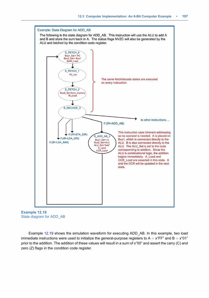
Example 12.19 shows the simulation waveform for executing ADD_AB. In this example, two load
immediate instructions were used to initialize the general-purpose registers to A ¼ x“FF” and B ¼ x“01”
prior to the addition. The addition of these values will result in a sum of x“00” and assert the carry (C) and
zero (Z) flags in the condition code register.
Example 12.18State diagram for ADD_AB
12.3 Computer Implementation: An 8-Bit Computer Example • 197
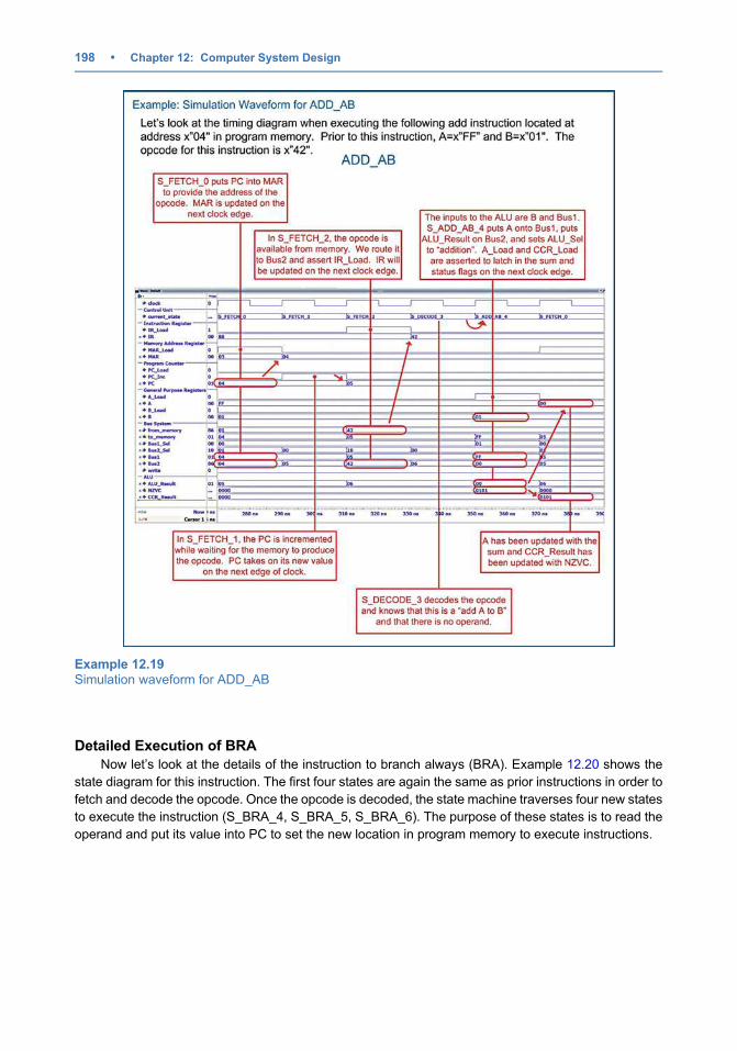
Detailed Execution of BRA
Now let’s look at the details of the instruction to branch always (BRA). Example 12.20 shows the
state diagram for this instruction. The first four states are again the same as prior instructions in order to
fetch and decode the opcode. Once the opcode is decoded, the state machine traverses four new states
to execute the instruction (S_BRA_4, S_BRA_5, S_BRA_6). The purpose of these states is to read the
operand and put its value into PC to set the new location in program memory to execute instructions.
Example 12.19Simulation waveform for ADD_AB
198 • Chapter 12: Computer System Design
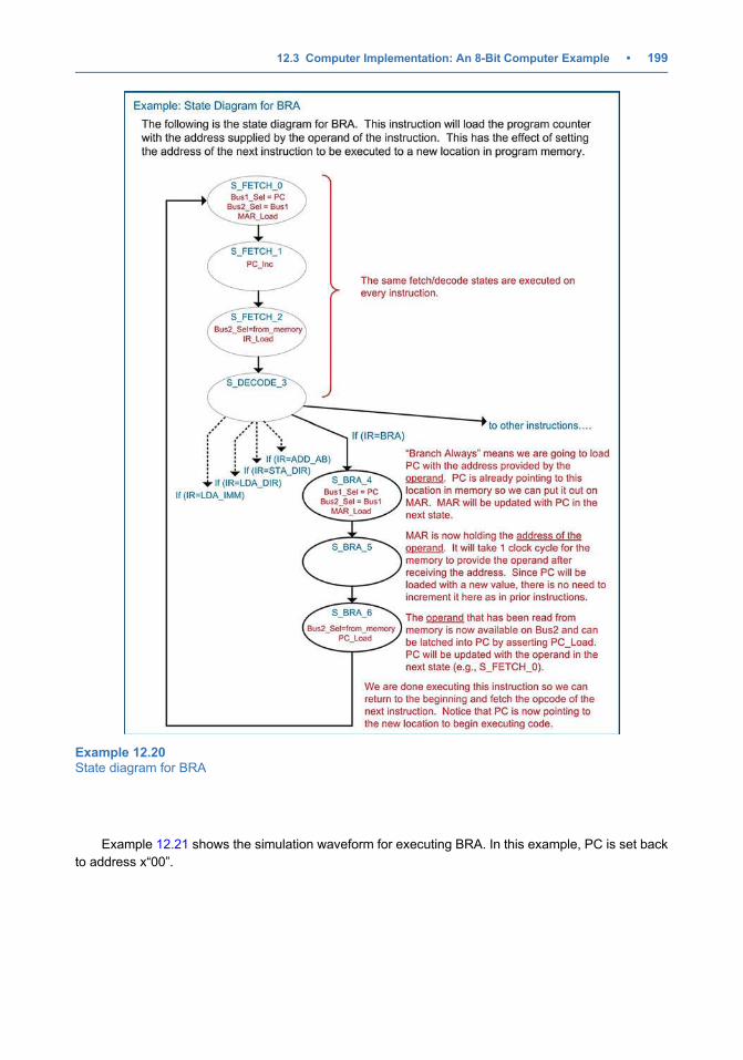
Example 12.21 shows the simulation waveform for executing BRA. In this example, PC is set back
to address x“00”.
Example 12.20State diagram for BRA
12.3 Computer Implementation: An 8-Bit Computer Example • 199
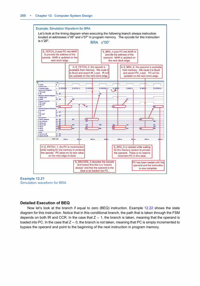
Detailed Execution of BEQ
Now let’s look at the branch if equal to zero (BEQ) instruction. Example 12.22 shows the state
diagram for this instruction. Notice that in this conditional branch, the path that is taken through the FSM
depends on both IR and CCR. In the case that Z ¼ 1, the branch is taken, meaning that the operand is
loaded into PC. In the case that Z¼ 0, the branch is not taken, meaning that PC is simply incremented to
bypass the operand and point to the beginning of the next instruction in program memory.
Example 12.21Simulation waveform for BRA
200 • Chapter 12: Computer System Design
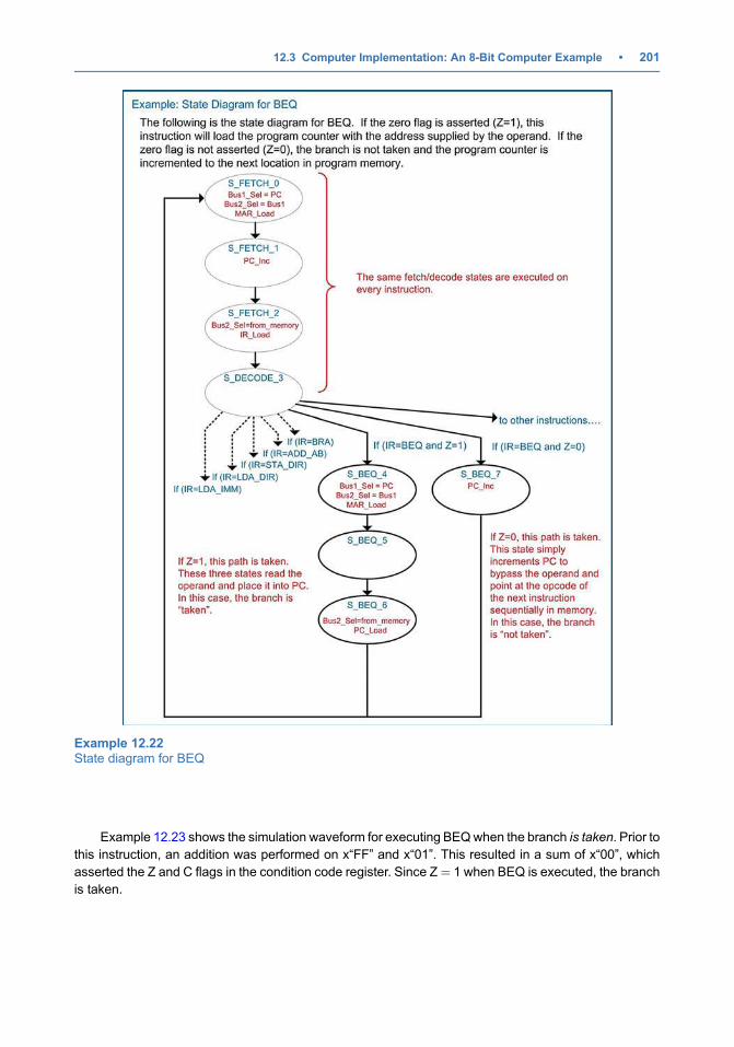
Example 12.23 shows the simulation waveform for executing BEQwhen the branch is taken. Prior to
this instruction, an addition was performed on x“FF” and x“01”. This resulted in a sum of x“00”, which
asserted the Z and C flags in the condition code register. Since Z¼ 1 when BEQ is executed, the branch
is taken.
Example 12.22State diagram for BEQ
12.3 Computer Implementation: An 8-Bit Computer Example • 201
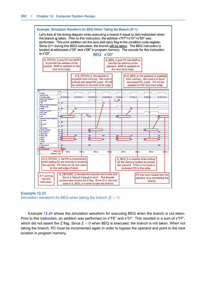
Example 12.24 shows the simulation waveform for executing BEQ when the branch is not taken.
Prior to this instruction, an addition was performed on x“FE” and x“01”. This resulted in a sum of x“FF”,
which did not assert the Z flag. Since Z ¼ 0 when BEQ is executed, the branch is not taken. When not
taking the branch, PC must be incremented again in order to bypass the operand and point to the next
location in program memory.
Example 12.23Simulation waveform for BEQ when taking the branch (Z ¼ 1)
202 • Chapter 12: Computer System Design
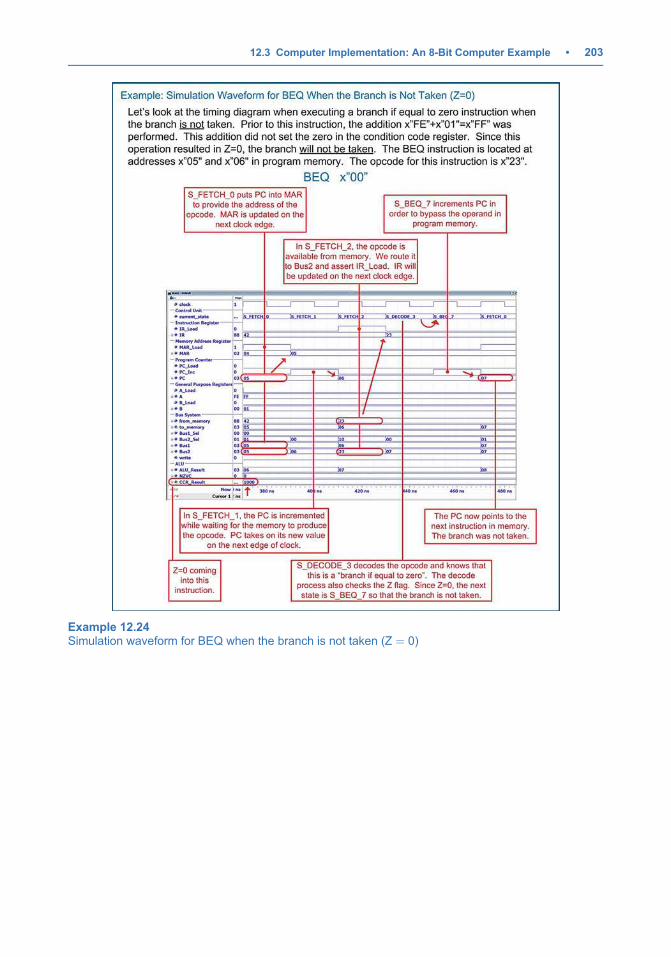
Example 12.24Simulation waveform for BEQ when the branch is not taken (Z ¼ 0)
12.3 Computer Implementation: An 8-Bit Computer Example • 203
CONCEPT CHECK
CC12.3 The 8-bit microcomputer example presented in this section is a very simple architec-ture used to illustrate the basic concepts of a computer. If we wanted to keep thiscomputer an 8-bit system but increase the depth of the memory, it would requireadding more address lines to the address bus. What changes to the computer systemwould need to be made to accommodate the wider address bus?
(A) The width of the program counter would need to be increased to support thewider address bus.
(B) The size of the memory address register would need to be increased tosupport the wider address bus.
(C) Instructions that use direct addressing would need additional bytes ofoperand to pass the wider address into the CPU 8-bits at a time.
(D) All of the above.
Summary
v A computer is a collection of hardwarecomponents that are constructed to performa specific set of instructions to process andstore data. The main hardware componentsof a computer are the central processing unit(CPU), program memory, data memory, andinput/output ports.
v TheCPUconsists of registers for fast storage,an arithmetic logic unit (ALU) for data manip-ulation, and a control state machine thatdirects all activity to execute an instruction.
v A CPU is typically organized into a data pathand a control unit. The data path containscircuitry used to store and process informa-tion. The data path includes registers and theALU. The control unit is a large state machinethat sends control signals to the data path inorder to facilitate instruction execution.
v The control unit performs a fetch-decode-execute cycle in order to completeinstructions.
v The instructions that a computer is designedto execute is called its instruction set.
v Instructions are inserted into program mem-ory in a sequence that when executed willaccomplish a particular task. This sequenceof instructions is called a computer program.
v An instruction consists of an opcode and apotential operand. The opcode is the uniquebinary code that tells the control statemachine which instruction is being executed.An operand is additional information that maybe needed for the instruction.
v An addressing mode refers to the way thatthe operand is treated. In immediateaddressing the operand is the actual data tobe used. In direct addressing the operand isthe address of where the data is to beretrieved or stored. In inherent addressingall of the information needed to completethe instruction is contained within the opcodeso no operand is needed.
v A computer also contains data memory tohold temporary variables during run time.
v A computer also contains input and outputports to interface with the outside world.
v A memory-mapped system is one in whichthe program memory, data memory, and I/Oports are all assigned a unique address. Thisallows the CPU to simply process informationas data and addresses and allows the pro-gram to handle where the information isbeing sent to. A memory map is a graphicalrepresentation of what address ranges vari-ous components are mapped to.
v There are three primary classes ofinstructions. These are loads and stores,data manipulations, and branches.
v Load instructions move information frommemory into a CPU register. A load instruc-tion takes multiple read cycles.
v Store instructions move information from aCPU register into memory. A store instructiontakes multiple read cycles and at least onewrite cycle.
204 • Chapter 12: Computer System Design
v Data manipulation instructions operate oninformation being held in CPU registers.Data manipulation instructions often useinherent addressing.
v Branch instructions alter the flow of instruc-tion execution. Unconditional branchesalways change the location in memory ofwhere the CPU is executing instructions.Conditional branches only change the
location of instruction execution if a statusflag is asserted.
v Status flags are held in the condition code reg-ister and are updated by certain instructions.The most commonly used flags are the nega-tive flag (N), zero flag (Z), two’s complementoverflow flag (V), and carry flag (C).
Exercise Problems
Section 12.1: Computer Hardware
12.1.1 What computer hardware sub-system holdsthe temporary variables used by the program?
12.1.2 What computer hardware sub-system containsfast storage for holding and/or manipulatingdata and addresses?
12.1.3 What computer hardware sub-system allowsthe computer to interface to the outside world?
12.1.4 What computer hardware sub-system containsthe state machine that orchestrates the fetch-decode-execute process?
12.1.5 What computer hardware sub-system containsthe circuitry that performs mathematical andlogic operations?
12.1.6 What computer hardware sub-system holdsthe instructions being executed?
Section 12.2: Computer Software
12.2.1 In computer software, what are the names ofthe most basic operations that a computer canperform?
12.2.2 Which element of computer software is thebinary code that tells the CPUwhich instructionis being executed?
12.2.3 Which element of computer software is a col-lection of instructions that perform a desiredtask?
12.2.4 Which element of computer software is thesupplementary information required by aninstruction such as constants or whichregisters to use?
12.2.5 Which class of instructions handles movinginformation between memory and CPUregisters?
12.2.6 Which class of instructions alters the flow ofprogram execution?
12.2.7 Which class of instructions alters data usingeither arithmetic or logical operations?
Section 12.3: Computer Implementa-
tion—An 8-Bit Computer Example
12.3.1 Design the example 8-bit computer systempresented in this chapter in VHDL with theability to execute the three instructionsLDA_IMM, STA_DIR, and BRA. Simulate yourcomputer system using the following programthat will continually write the patterns x“AA”and x“BB” to output ports port_out_00 andport_out_01:
constant ROM : rom_type :¼ (
0 ¼> LDA_IMM,
1 ¼> x"AA",
2 ¼> STA_DIR,
3 ¼> x"E0",
4 ¼> STA_DIR,
5 ¼> x"E1",
6 ¼> LDA_IMM,
7 ¼> x"BB",
8 ¼> STA_DIR,
9 ¼> x"E0",
10 ¼> STA_DIR,
11 ¼> x"E1",
12 ¼> BRA,
13 ¼> x"00",
others ¼> x"00");
12.3.2 Add the functionality to the computer modelfrom 12.3.1 the ability to perform the LDA_DIRinstruction. Simulate your computer systemusing the following program that will continuallyread from port_in_00 and write its contents toport_out_00:
constant ROM : rom_type :¼ (
0 ¼> LDA_DIR,
1 ¼> x"F0",
2 ¼> STA_DIR,
3 ¼> x"E0",
4 ¼> BRA,
5 ¼> x"00",
others ¼> x"00");
Exercise Problems • 205
12.3.3 Add the functionality to the computer modelfrom 12.3.2 the ability to perform theinstructions LDB_IMM, LDB_DIR, andSTB_DIR. Modify the example programsgiven in exercise 12.3.1 and 12.3.2 to useregister B in order to simulate yourimplementation.
12.3.4 Add the functionality to the computer modelfrom 12.3.3 the ability to perform the additioninstruction ADD_AB. Test your addition instruc-tion by simulating the following program. Thefirst addition instruction will performx“FE” + x“01” ¼ x“FF” and assert the negative(N) flag. The second addition instruction willperform x“FF” + x“01” ¼ x“00” and assert thecarry (C) and zero (Z) flags. The third additioninstruction will perform x“7F” + x“7F” ¼ x“FE”and assert the two’s complement overflow (V)and negative (N) flags.
constant ROM : rom_type :¼ (
0 ¼> LDA_IMM, -- A¼x”FE”
1 ¼> x"FE",
2 ¼> LDB_IMM, -- B¼x”01”
3 ¼> x"01",
4 ¼> ADD_AB, -- A¼A+B
5 ¼> LDA_IMM, -- A¼x”FF”
6 ¼> x"FF",
7 ¼> LDB_IMM, -- B¼x”01”
8 ¼> x"01",
9 ¼> ADD_AB, -- A¼A+B
10 ¼> LDA_IMM, -- A¼x”7F”
11 ¼> x"7F",
12 ¼> LDB_IMM, -- B¼x”7F”
13 ¼> x"7F",
14 ¼> ADD_AB, -- A¼A+B
15 ¼> BRA,
16 ¼> x"00",
others ¼> x"00");
12.3.5 Add the functionality to the computer modelfrom 12.3.4 the ability to perform the branch ifequal to zero instruction BEQ. Simulate yourimplementation using the following program.The first addition in this program will performx“FE” + x“01” ¼ x“FF” (Z ¼ 0). The subsequentBEQ instruction should NOT take the branch.The second addition in this program will per-form x“FF” + x“01” ¼ x“00” (Z ¼ 1) andSHOULD take the branch. The final instructionin this program is a BRA that is inserted forsafety. In the event that the BEQ is notoperating properly, the BRA will set the pro-gram counter back to x“00” and prevent theprogram from running away.
constant ROM : rom_type :¼ (
0 ¼> LDA_IMM,
1 ¼> x"FE",
2 ¼> LDB_IMM,
3 ¼> x"01",
4 ¼> ADD_AB,
5 ¼> BEQ,
6 ¼> x”00”, -- should not
-- branch
7 ¼> LDA_IMM,
8 ¼> x"FF",
9 ¼> LDB_IMM,
10 ¼> x"01",
11 ¼> ADD_AB,
12 ¼> BEQ,
13 ¼> x”00”, -- should
-- branch
14 ¼> BRA,
15 ¼> x"00",
others ¼> x"00");
206 • Chapter 12: Computer System Design
Appendix A: List of Worked Examples
EXAMPLE 2.1 DEFINING VHDL ENTITIES ............................................................................................................................ 17
EXAMPLE 3.1 SOP LOGIC CIRCUIT: VHDL MODELING USING LOGICAL OPERATORS ................................................................... 25
EXAMPLE 3.2 3-TO-8 ONE-HOT DECODER: VHDL MODELING USING LOGICAL OPERATORS ......................................................... 26
EXAMPLE 3.3 7-SEGMENT DISPLAY DECODER: TRUTH TABLE .................................................................................................. 27
EXAMPLE 3.4 7-SEGMENT DISPLAY DECODER: LOGIC SYNTHESIS BY HAND .............................................................................. 28
EXAMPLE 3.5 7-SEGMENT DISPLAY DECODER: VHDL MODELING USING LOGICAL OPERATORS .................................................... 29
EXAMPLE 3.6 4-TO-2 BINARY ENCODER: LOGIC SYNTHESIS BY HAND ..................................................................................... 30
EXAMPLE 3.7 4-TO-2 BINARY ENCODER: VHDL MODELING USING LOGICAL OPERATORS .......................................................... 31
EXAMPLE 3.8 4-TO-1 MULTIPLEXER: VHDL MODELING USING LOGICAL OPERATORS ................................................................ 32
EXAMPLE 3.9 1-TO-4 DEMULTIPLEXER: VHDL MODELING USING LOGICAL OPERATORS ............................................................. 33
EXAMPLE 3.10 SOP LOGIC CIRCUIT: VHDL MODELING USING CONDITIONAL SIGNAL ASSIGNMENTS ............................................ 35
EXAMPLE 3.11 3-TO-8 ONE-HOT DECODER: VHDL MODELING USING CONDITIONAL SIGNAL ASSIGNMENTS .................................. 36
EXAMPLE 3.12 7-SEGMENT DISPLAY DECODER: VHDL MODELING USING CONDITIONAL SIGNAL ASSIGNMENTS .............................. 37
EXAMPLE 3.13 4-TO-2 BINARY ENCODER: VHDL MODELING USING CONDITIONAL SIGNAL ASSIGNMENTS .................................... 38
EXAMPLE 3.14 4-TO-1 MULTIPLEXER: VHDL MODELING USING CONDITIONAL SIGNAL ASSIGNMENTS .......................................... 39
EXAMPLE 3.15 1-TO-4 DEMULTIPLEXER: VHDL MODELING USING CONDITIONAL SIGNAL ASSIGNMENTS ....................................... 40
EXAMPLE 3.16 SOP LOGIC CIRCUIT: VHDL MODELING USING SELECTED SIGNAL ASSIGNMENTS ................................................ 42
EXAMPLE 3.17 3-TO-8 ONE-HOT DECODER: VHDL MODELING USING SELECTED SIGNAL ASSIGNMENTS ....................................... 43
EXAMPLE 3.18 7-SEGMENT DISPLAY DECODER: VHDL MODELING USING SELECTED SIGNAL ASSIGNMENTS .................................. 44
EXAMPLE 3.19 4-TO-2 BINARY ENCODER: VHDL MODELING USING SELECTED SIGNAL ASSIGNMENTS ........................................ 45
EXAMPLE 3.20 4-TO-1 MULTIPLEXER: VHDL MODELING USING SELECTED SIGNAL ASSIGNMENTS .............................................. 46
EXAMPLE 3.21 1-TO-4 DEMULTIPLEXER: VHDL MODELING USING SELECTED SIGNAL ASSIGNMENTS ........................................... 47
EXAMPLE 3.22 MODELING LOGIC USING DELAYED SIGNAL ASSIGNMENTS (INERTIAL DELAY MODEL) .............................................. 48
EXAMPLE 3.23 MODELING LOGIC USING DELAYED SIGNAL ASSIGNMENTS (TRANSPORT DELAY MODEL) ........................................... 49
EXAMPLE 4.1 MODELING LOGIC USING STRUCTURAL VHDL (EXPLICIT PORT MAPPING) ............................................................. 54
EXAMPLE 4.2 MODELING LOGIC USING STRUCTURAL VHDL (POSITIONAL PORT MAPPING) ......................................................... 55
EXAMPLE 4.3 DESIGN OF A HALF ADDER ............................................................................................................................. 56
EXAMPLE 4.4 DESIGN OF A FULL ADDER ............................................................................................................................ 57
EXAMPLE 4.5 DESIGN OF A FULL ADDER OUT OF HALF ADDERS ............................................................................................. 58
EXAMPLE 4.6 DESIGN OF A 4-BIT RIPPLE CARRY ADDER (RCA) ............................................................................................ 59
EXAMPLE 4.7 STRUCTURAL MODEL OF A FULL ADDER IN VHDL USING TWO HALF ADDERS ....................................................... 60
EXAMPLE 4.8 STRUCTURAL MODEL OF A 4-BIT RIPPLE CARRY ADDER IN VHDL ...................................................................... 61
EXAMPLE 5.1 BEHAVIOR OF SEQUENTIAL SIGNAL ASSIGNMENTS WITHIN A PROCESS .................................................................. 68
EXAMPLE 5.2 BEHAVIOR OF CONCURRENT SIGNAL ASSIGNMENTS OUTSIDE A PROCESS ............................................................... 68
EXAMPLE 5.3 VARIABLE ASSIGNMENT BEHAVIOR .................................................................................................................. 69
EXAMPLE 5.4 USING IF/THEN STATEMENTS TO MODEL COMBINATIONAL LOGIC .......................................................................... 71
EXAMPLE 5.5 USING CASE STATEMENTS TO MODEL COMBINATIONAL LOGIC .............................................................................. 73
EXAMPLE 5.6 BEHAVIORAL MODELING OF A RISING EDGE TRIGGERED D-FLIP-FLOP USING ATTRIBUTES ........................................ 77
EXAMPLE 6.1 BEHAVIORAL MODELING OF A D-FLIP-FLOP USING THE RISING_EDGE() FUNCTION .................................................. 84
EXAMPLE 6.2 BEHAVIORAL MODEL OF A 4-BIT ADDER IN VHDL ............................................................................................. 87
EXAMPLE 7.1 CREATING A VHDL TEST BENCH ................................................................................................................. 100
EXAMPLE 7.2 VHDL TEST BENCH FOR A 4-BIT RIPPLE CARRY ADDER USING NESTED FOR LOOPS ............................................. 101
EXAMPLE 7.3 USING REPORT STATEMENTS IN A VHDL TEST BENCH ..................................................................................... 103
EXAMPLE 7.4 USING ASSERT STATEMENTS IN A VHDL TEST BENCH .................................................................................... 104
EXAMPLE 7.5 WRITING TO AN EXTERNAL FILE FROM A TEST BENCH (PART 1) ....................................................................... 105
EXAMPLE 7.6 WRITING TO AN EXTERNAL FILE FROM A TEST BENCH (PART 2) ....................................................................... 106
EXAMPLE 7.7 WRITING TO AN EXTERNAL FILE FROM A TEST BENCH (PART 3) ....................................................................... 107
EXAMPLE 7.8 WRITING TO STD_OUT FROM A TEST BENCH (PART 1) ............................................................................... 108
EXAMPLE 7.9 WRITING TO STD_OUT FROM A TEST BENCH (PART 2) ............................................................................... 109
EXAMPLE 7.10 READING FROM AN EXTERNAL FILE IN A TEST BENCH (PART 1) ...................................................................... 109
EXAMPLE 7.11 READING FROM AN EXTERNAL FILE IN A TEST BENCH (PART 2) ...................................................................... 110
# Springer Nature Switzerland AG 2019
B. J. LaMeres, Quick Start Guide to VHDL, https://doi.org/10.1007/978-3-030-04516-6
207
EXAMPLE 7.12 READING FROM AN EXTERNAL FILE IN A TEST BENCH (PART 3) ......................................................................111
EXAMPLE 7.13 READING SPACE-DELIMITED DATA FROM AN EXTERNAL FILE IN A TEST BENCH (PART 1) ......................................111
EXAMPLE 7.14 READING SPACE-DELIMITED DATA FROM AN EXTERNAL FILE IN A TEST BENCH (PART 2) ..................................... 112
EXAMPLE 7.15 READING SPACE-DELIMITED DATA FROM AN EXTERNAL FILE IN A TEST BENCH (PART 3) ..................................... 113
EXAMPLE 8.1 BEHAVIORAL MODEL OF A D-LATCH IN VHDL .............................................................................................. 117
EXAMPLE 8.2 BEHAVIORAL MODEL OF A D-FLIP-FLOP IN VHDL .......................................................................................... 118
EXAMPLE 8.3 BEHAVIORAL MODEL OF A D-FLIP-FLOP WITH ASYNCHRONOUS RESET IN VHDL ................................................. 119
EXAMPLE 8.4 BEHAVIORAL MODEL OF A D-FLIP-FLOP WITH ASYNCHRONOUS RESET AND PRESET IN VHDL ............................... 120
EXAMPLE 8.5 BEHAVIORAL MODEL OF A D-FLIP-FLOP WITH SYNCHRONOUS ENABLE IN VHDL ................................................. 121
EXAMPLE 8.6 RTL MODEL OF AN 8-BIT REGISTER IN VHDL ............................................................................................... 122
EXAMPLE 8.7 RTL MODEL OF A 4-STAGE, 8-BIT SHIFT REGISTER IN VHDL ......................................................................... 123
EXAMPLE 8.8 REGISTERS AS AGENTS ON A DATA BUS: SYSTEM TOPOLOGY ........................................................................... 124
EXAMPLE 8.9 REGISTERS AS AGENTS ON A DATA BUS: RTL MODEL IN VHDL ........................................................................ 124
EXAMPLE 8.10 REGISTERS AS AGENTS ON A DATA BUS: SIMULATION WAVEFORM ..................................................................... 125
EXAMPLE 9.1 PUSH-BUTTON WINDOW CONTROLLER IN VHDL: DESIGN DESCRIPTION .............................................................. 128
EXAMPLE 9.2 PUSH-BUTTON WINDOW CONTROLLER IN VHDL: ENTITY DEFINITION ................................................................. 128
EXAMPLE 9.3 PUSH-BUTTON WINDOW CONTROLLER IN VHDL: ARCHITECTURE ....................................................................... 131
EXAMPLE 9.4 PUSH-BUTTON WINDOW CONTROLLER IN VHDL: SIMULATION WAVEFORM .......................................................... 131
EXAMPLE 9.5 PUSH-BUTTON WINDOW CONTROLLER IN VHDL: EXPLICIT STATE CODES ........................................................... 132
EXAMPLE 9.6 SERIAL BIT SEQUENCE DETECTOR IN VHDL: DESIGN DESCRIPTION AND ENTITY DEFINITION .................................. 133
EXAMPLE 9.7 SERIAL BIT SEQUENCE DETECTOR IN VHDL: ARCHITECTURE ........................................................................... 134
EXAMPLE 9.8 SERIAL BIT SEQUENCE DETECTOR IN VHDL: SIMULATION WAVEFORM ................................................................ 134
EXAMPLE 9.9 VENDING MACHINE CONTROLLER IN VHDL: DESIGN DESCRIPTION AND ENTITY DEFINITION ................................... 135
EXAMPLE 9.10 VENDING MACHINE CONTROLLER IN VHDL: ARCHITECTURE .......................................................................... 136
EXAMPLE 9.11 VENDING MACHINE CONTROLLER IN VHDL: SIMULATION WAVEFORM ................................................................ 137
EXAMPLE 9.12 2-BIT BINARY UP/DOWN COUNTER IN VHDL: DESIGN DESCRIPTION AND ENTITY DEFINITION ............................... 137
EXAMPLE 9.13 2-BIT BINARY UP/DOWN COUNTER IN VHDL: ARCHITECTURE (THREE PROCESS MODEL) .................................... 138
EXAMPLE 9.14 2-BIT BINARY UP/DOWN COUNTER IN VHDL: SIMULATION WAVEFORM ............................................................. 139
EXAMPLE 10.1 4-BIT BINARY UP COUNTER IN VHDL USING THE TYPE UNSIGNED ............................................................ 144
EXAMPLE 10.2 4-BIT BINARY UP COUNTER IN VHDL USING THE TYPE INTEGER .............................................................. 145
EXAMPLE 10.3 4-BIT BINARY UP COUNTER IN VHDL USING THE TYPE STD_LOGIC_VECTOR (1) ................................... 146
EXAMPLE 10.4 4-BIT BINARY UP COUNTER IN VHDL USING THE TYPE STD_LOGIC_VECTOR (2) ....................................... 147
EXAMPLE 10.5 4-BIT BINARY UP COUNTER WITH ENABLE IN VHDL .................................................................................... 148
EXAMPLE 10.6 4-BIT BINARY UP COUNTER WITH LOAD IN VHDL ......................................................................................... 149
EXAMPLE 11.1 BEHAVIORAL MODEL OF A 4 � 4 ASYNCHRONOUS READ ONLY MEMORY IN VHDL ............................................ 156
EXAMPLE 11.2 BEHAVIORAL MODEL OF A 4 � 4 SYNCHRONOUS READ ONLY MEMORY IN VHDL ............................................. 157
EXAMPLE 11.3 BEHAVIORAL MODEL OF A 4 � 4 ASYNCHRONOUS READ/WRITE MEMORY IN VHDL .......................................... 159
EXAMPLE 11.4 BEHAVIORAL MODEL OF A 4 � 4 SYNCHRONOUS READ/WRITE MEMORY IN VHDL ............................................. 160
EXAMPLE 12.1 MEMORY MAP FOR A 256 � 8 MEMORY SYSTEM ......................................................................................... 168
EXAMPLE 12.2 EXECUTION OF AN INSTRUCTION TO “LOAD REGISTER A USING IMMEDIATE ADDRESSING” .................................... 171
EXAMPLE 12.3 EXECUTION OF AN INSTRUCTION TO “LOAD REGISTER A USING DIRECT ADDRESSING” ........................................ 172
EXAMPLE 12.4 EXECUTION OF AN INSTRUCTION TO “STORE REGISTER A USING DIRECT ADDRESSING” ...................................... 173
EXAMPLE 12.5 EXECUTION OF AN INSTRUCTION TO “ADD REGISTERS A AND B” .................................................................... 174
EXAMPLE 12.6 EXECUTION OF AN INSTRUCTION TO “BRANCH ALWAYS” .................................................................................. 175
EXAMPLE 12.7 EXECUTION OF AN INSTRUCTION TO “BRANCH IF EQUAL TO ZERO” .................................................................. 176
EXAMPLE 12.8 TOP-LEVEL BLOCK DIAGRAM FOR THE 8-BIT COMPUTER SYSTEM .................................................................... 178
EXAMPLE 12.9 INSTRUCTION SET FOR THE 8-BIT COMPUTER SYSTEM ................................................................................... 179
EXAMPLE 12.10 MEMORY SYSTEM BLOCK DIAGRAM FOR THE 8-BIT COMPUTER SYSTEM .......................................................... 180
EXAMPLE 12.11 CPU BLOCK DIAGRAM FOR THE 8-BIT COMPUTER SYSTEM .......................................................................... 184
EXAMPLE 12.12 STATE DIAGRAM FOR LDA_IMM ............................................................................................................ 191
EXAMPLE 12.13 SIMULATION WAVEFORM FOR LDA_IMM .................................................................................................. 192
EXAMPLE 12.14 STATE DIAGRAM FOR LDA_DIR ............................................................................................................. 193
EXAMPLE 12.15 SIMULATION WAVEFORM FOR LDA_DIR .................................................................................................. 194
EXAMPLE 12.16 STATE DIAGRAM FOR STA_DIR ............................................................................................................. 195
EXAMPLE 12.17 SIMULATION WAVEFORM FOR STA_DIR .................................................................................................. 196
EXAMPLE 12.18 STATE DIAGRAM FOR ADD_AB .............................................................................................................. 197
EXAMPLE 12.19 SIMULATION WAVEFORM FOR ADD_AB ................................................................................................... 198
208 • Appendix A: List of Worked Examples
EXAMPLE 12.20 STATE DIAGRAM FOR BRA ..................................................................................................................... 199
EXAMPLE 12.21 SIMULATION WAVEFORM FOR BRA .......................................................................................................... 200
EXAMPLE 12.22 STATE DIAGRAM FOR BEQ .................................................................................................................... 201
EXAMPLE 12.23 SIMULATION WAVEFORM FOR BEQ WHEN TAKING THE BRANCH (Z ¼ 1) ...................................................... 202
EXAMPLE 12.24 SIMULATION WAVEFORM FOR BEQ WHEN THE BRANCH IS NOT TAKEN (Z ¼ 0) .............................................. 203
Appendix A: List of Worked Examples • 209
Index
A
Abstraction, 4
Adders
in VHDL, 59
C
Capacity, 153
Classical digital design flow, 8
Computer system design, 163
addressing modes, 169
arithmetic logic unit (ALU), 165
central processing unit, 165
condition code register, 165
control unit, 165
data memory, 164
data path, 165
direct addressing, 170
example 8-bit system, 177
control unit, 188
CPU, 184
data path, 185detailed instruction execution, 190
instruction set, 178
memory system, 179
general purpose registers, 165
hardware, 163
immediate addressing, 169
inherent addressing, 170
input output ports, 164
instruction register, 165
instructions, 163
branches, 174
data manipulations, 173
loads and stores, 170
memory address register, 165
memory mapped system, 166
memory map, 167
opcodes, 169
operands, 169
program, 163
program counter, 165
program memory, 164
registers, 165
software, 163, 169
Counters, 143
modeling in VHDL, 143
D
Demultiplexer design by hand, 32, 39, 46
Demultiplexer, 32, 39, 46
Design abstraction, 4
Design domains, 5
behavioral domain, 5
physical domain, 5
structural domain, 5
Design levels, 5
algorithmic level, 5
circuit level, 5
gate level, 5
register transfer level, 5
system level, 5
Digital design flow, 8
F
Finite state machines (FSM)
behavioral modeling in VHDL, 127
Full adders, 56
G
Gajski and Kuhn’s Y-chart, 5
H
Half adders, 56
History of HDLs, 1
M
Memory map model, 153
Modern digital design flow, 8
Multiplexer design by hand, 31, 38, 45
Multiplexers, 31, 38, 45
N
Nonvolatile memory, 154
O
One-hot binary encoder design by hand, 29
One-hot binary encoder modeling in VHDL, 29
One-hot decoder modeling in VHDL, 26, 35, 42
P
Place and route, 8
R
Random access memory (RAM), 155
Read cycle, 153
Read only memory (ROM), 154
Read/write (RW) memory, 154
Ripple carry adders (RCA), 58
# Springer Nature Switzerland AG 2019
B. J. LaMeres, Quick Start Guide to VHDL, https://doi.org/10.1007/978-3-030-04516-6
211
S
Semiconductor memory, 153
Sequential access memory, 155
7-Segment decoder design by hand, 27
7-Segment decoder modeling in VHDL, 28
T
Technology mapping, 8
V
Verification, 6
Verilog HDL, 2
VHDL behavioral modeling techniques
adders, 59
counters, 143
using type INTEGER, 144
using type STD_LOGIC_VECTOR, 145
using type UNSIGNED, 143with enables, 148
with loads, 149
D-flip-flops, 118
D-latches, 117
finite state machines, 127
explicit state encoding using subtypes, 132three process model, 129
user-enumerated state encoding, 129
modeling agents on a bus, 123
modeling memory, 155
modeling registers, 122
modeling shift registers, 122
VHDL constructs, 16
architecture, 16, 17
assignment operator (<¼), 21
attributes, 76
case statements, 71
component declaration, 19
concatenation operator, 24
concurrent signal assignments, 24
concurrent signal assignments with logical operators, 25
conditional signal assignments, 34
constant declaration, 19
data types, 13
delayed signal assignments, 48
inertial, 48
transport, 48
entity, 16
entity definition, 17
for loops, 75
if/then statements, 70
libraries and packages, 17
logical operators, 22
loop statements, 74
numerical operators, 23
operators, 21
packages, 16
process, 65
sensitivity list, 65wait statement, 66
relational operators, 23
selected signal assignments, 41
sequential signal assignments, 67
shift operators, 23
signal declaration, 18
structural design, 53
component declaration, 19
component instantiation, 53
explicit port mapping, 53
port mapping, 53positional port mapping, 55
test benches, 99
assert statements, 103reading/writing external files, 89
report statements, 102
variables, 68
while loops, 75
VHDL data types
array, 15
bit, 13
bit_vector, 14
boolean, 13
character, 13
integer, 14
natural, 15
real, 14
std_logic, 81
std_logic_vector, 81
std_ulogic, 81
std_ulogic_vector, 81
string, 14
time, 14
user-defined enumerated, 15
VHDL packages, 81
MATH_COMPLEX, 95
MATH_REAL, 93
NUMERIC_BIT, 92
NUMERIC_BIT_UNSIGNED, 93
NUMERIC_STD, 85
conversion functions, 88
type casting, 88
NUMERIC_STD_UNSIGNED, 92
standard, 16
STD_LOGIC_1164, 81
resolution function, 82
type conversions, 84
STD_LOGIC_ARITH, 95
STD_LOGIC_SIGNED, 96
STD_LOGIC_TEXTIO, 89
STD_LOGIC_UNSIGNED, 96
TEXTIO, 89
Volatile memory, 154
W
Write cycle, 153
Y
Y-chart, 5
212 • Index