quantum photonic integrated circuits - univer · quantum photonic integrated circuits ... all these...
TRANSCRIPT

Hauptseminar: Nanooptik und Nanophotonik
QUANTUM PHOTONIC INTEGRATED CIRCUITS
Submitted: 19.07.2016Author: Marco NageleInstitute: Institut fur Halbleiteroptik und Funktionelle GrenzflachenSupervisor: Prof. Dr. Peter Michler

Contents
1 Introduction 1
2 Basics and Material Platforms 12.1 Material Platforms . . . . . . . . . . . . . . . . . . . . . . . . . . . . . . . . . . . . . . 22.2 Direct Laser Writing . . . . . . . . . . . . . . . . . . . . . . . . . . . . . . . . . . . . . 22.3 Light Propagation in Waveguides . . . . . . . . . . . . . . . . . . . . . . . . . . . . . . 2
3 Photon Generation 33.1 Parametric Down-Conversion - AlN Microring Resonator . . . . . . . . . . . . . . . 3
4 Manipulation of Quantum States 44.1 Hong-Ou-Mandel Effect . . . . . . . . . . . . . . . . . . . . . . . . . . . . . . . . . . . 54.2 Directional Coupler . . . . . . . . . . . . . . . . . . . . . . . . . . . . . . . . . . . . . . 64.3 Quantum Dots embedded in Waveguides . . . . . . . . . . . . . . . . . . . . . . . . . 84.4 Mach-Zehnder Interferometer . . . . . . . . . . . . . . . . . . . . . . . . . . . . . . . . 9
5 Single Photon Detection with Superconducting Nanowires 11
6 Future Directions and Summary 11
1 Introduction
Quantum technology offers significant opportunities for communication security, computationalefficiency and measurement precision. This pioneering field of research is located at the interfaceof physical and information science and promises to revolutionize information technology byharnessing unique properties of quantum mechanics to encode, transmit and process information.Hereby photons are used as qbits while superposition and entanglement plays a crucial role.To date, many quantum photonic experiments have been realized using large-scaled opticalelements, such as mirrors or beam splitters, bolted onto optical benches. Because of the physicalsize and bulk components, these setups are limited regarding stability, complexity and scalability.In contrast photonic integrated circuits provide sub-wavelength stability of optical path lengthsfor high visibility and on-chip quantum state manipulation, generation and detection.In 2000, it was shown by Knill, Laflamme and Milburn that it is theoretically possible to create auniversal quantum computation scheme solely with linear optics. Their work, which has becomefamous as KLM protocol, only uses linear optical elements, single photon sources and photondetectors as modules to implement a quantum computation scheme. [1]All these necessary components such as integrated single-photon sources, linear optical elementsand photon detectors have been implemented separately and on different material platforms,partially supported by external devices. These days, main goal of information science is tomerge those components together in order to fabricate first fully functional standalone photonicintegrated circuit.This work should give a idea about the fundamentals of photonic integrated circuits as well as thecurrent state of art.
2 Basics and Material Platforms
In photonic integrated circuits, photons are used as qbits as they offer some tempting properties.Besides low decoherence, photons provide high speed lossless transmission, compatibility withmature and well understand classical photonic technology and they can easily be manipulatedas well as encoded with several degrees of freedom. These degrees of freedom are for examplepolarization, path, time or orbital angular momentum.A big drawback in comparison to electrons is the small mutual photon interaction length. This lackof achieving nonlinear effects restricts implementation of deterministic gates. Only probabilisticgates, linked to a certain working probability are possible.As already indicated, photonic integrated circuit can be realized using several material platformslinked to certain fabrication methods. Various platforms provide different advantages as wellas downsides. A big range of materials such III-V semiconductor, Silica-on-Silicon, AluminumNitride (AlN) and Polymer Integration Platforms, can be used.Several techniques are used to fabricate different material based systems. Photo-lithography ismost commonly used for platforms, such as III-V Semiconductor. Beside that, direct laser writingin glass offers great potential and 3D spatial component arrangement.Since III-V Semiconductor and Silica-on-Silicon are the most common materials it might beinteresting to investigate their properties more precisely. Also, it might be worth to have a brieflook at AlN since this is relatively new material, offering useful applications.
∣∣∣∣∣ 1

2.1 Material Platforms
As an example of III-V Semiconductor, Gallium Arsenide (GaAs) has a direct-band gap whichenables on-chip single-photon sources like quantum dots embedded in GaAs photonic crystalwaveguides. The high refractive index offers tight light confinement and therefore compactdevices. GaAs has a large χ(2) nonlinear coefficient and thus a large electro-optical effect enablesfast device switching. This provides fast routing and on-chip photon manipulation. For thismaterial, entangled photon pairs can be generated via spontaneous parametric down conversion(SPDC). A big disadvantage of GaAs are high fabrication costs, what could be solved with newfabrication methods in future.Silica-on-Silicon is also a popular material for integrated circuits. It is an indirect band-gapmaterial, which means an external light source is needed. Since it has a good fiber coupling, this ispossible with low losses. The refractive index can be modulated using thermo-optical effect sinceχ(2) is small. Compared to electro-optical effect, this impedes fast switching. In contrast to GaAs,Silica-on-Silicon can be fabricated very cheap and is compatible with Si-based microelectronics.
Aluminium Nitride (AlN) is a relatively new material used for photonic integrated circuits.Its strong χ(2) enables strong second order nonlinearities for fast switching. Additionally SPDCphoton generation is possible with high efficiency and low integrated loss. Similar to Silica-on-Silicon this platform does not provide on-chip photon generation and therefore externalcomponents are necessary.
2.2 Direct Laser Writing
Direct laser writing is an excellent technique for the fabrication of photonic integrated circuitsin glass and therefore it is worth going more into detail. A big advantage compared to photo-lithography is, that it offers fast and very complex structure design. In order to write anystructure, a femtosecond pulse is tightly focused in glass where high photon density leads tomultiphoton absorption and avalanche ionization. Avalanche ionization occurs because theelectrons in the conduction band of the dielectric are accelerated in such a way that they ionizeatoms and molecules like an avalanche. The result is an induced permanent and localizedrefractive index only at the focus. Design potential is versatile because the desired structure iswritten by translation of the sample with respect to the laser.There are several positive characterisitcs regarding direct laser written waveguides. The createdrefractive index modulation has a circular symmetric transverse profile, which is ideal for Gaussianshaped beams. Also fabrication is quite fast compared to etching methods with a writing speed ofabout 4cm/s. As already mentioned, this technique provides very complex and also 3D spatialstructure design and exhibit low birefringence.
2.3 Light Propagation in Waveguides
As already implied, light propagates on-chip in waveguides. Light propagation is based on internaltotal reflection between refractive index interfaces. Main part is a core which is surrounded bya cladding exhibiting a slightly lower refractive index, shown in Figure 1 a). Also the claddingburies the core and isolates from surrounding environment.
2
∣∣∣∣∣

F igure 1: Light propagation in waveguides. (a) Schematic profile of a waveguide with its necessary components [2].(b) SEM micrograph taken of a SiNx waveguide in cross-section [3].
Depending on the device, a buffer layer is necessary to separate waveguide from higher refractiveindex substrate, guaranteeing total reflection.For efficient and fast data transfer, dispersion properties are important. All higher modes exceptthe fundamental mode need to be suppressed. This condition can be achieved by choosing certainlateral and vertical waveguide dimensions. Planar waveguides provide useful possibilities such asoptical modulation via thermo-optical effect n(∆T) = n0 + α · ∆T.Here, the refractive index is changed linearly by modification of temperature, where alpha isas a material dependent coefficient. This means refractive index and therefore optical phasemodulation is possible, only by changing temperature of an attached heating resistor.On the right-hand side of Figure 1, a cross-section of a silicon nitride waveguide for low noisefrequency propagation is shown with numerical simulations of a transverse optical beam profile.It is obvious that intensity possess radial intensity distribution and therefore evanescent fieldoccurs even outside the waveguide. This evanescent, exponentially decaying field is used insubsequent chapters to implement directional couplers and Mach-Zehnder interferometer.
3 Photon Generation
Photon generation is a crucial issue regarding photonic integrated chips. To date, not everymaterial platform has an on-chip solution and hence external photon sources remedy. Whilequantum dots as single photon sources are feasible, parametric down-conversion is used togenerate entangled photon pairs.
3.1 Parametric Down-Conversion - AlN Microring Resonator
The relatively new AlN material platform offers strong second order nonlinearity and is anexcellent candidate for parametric down-conversion of photons in order to achieve entangledphoton pairs. Beside that, large nonlinearity provides strong electro-optical response and thereforehigh-speed phase modulation.On-chip microring resonators with high Q-factors (see Figure 2 a) )can be used to further improveinteraction between pump photons and the nonlinear coefficient χ(2).Due to SPDC it is possible to convert a visible pump photon at 775nm into a 1550nm telecommu-nication wavelength photon pairs.
∣∣∣∣∣ 3

F igure 2: On-chip AlN SPDC source. (a) High Q-factor AlN microring with IR waveguide (top) and visible lightwaveguide (bottom). (b) Effective refractive indices are matched using different modes (shown as insets on the right).Phase matching is achieved when the waveguide width is around 1.1µm. Cross-section of a AlN microring is depcitedin the left lower inset [4]
.
It is obvious that energy conservation as well as momentum conservation
ω775nm = ω1550nm + ω1550nm p775nm = p1550nm + p1550nm (1)
needs to be fulfilled. For efficient conversion, the refractive indices of pump and convertedphotons has to match. The refractive index inside such a microring is given by
ne f f =pxcωxr
(2)
where px is the momentum, ωx the microring waveguide width while r is its radius. This means,it is possible to get a refractive index change by waveguide width modulation. Furthermore, itis possible to use different transverse light polarization to further influence the refractive indexas a function of waveguide width. Phase match condition is satisfied with a waveguide widtharound 1.10µm whereas pump photons have TM2 polarization while TM0 polarization is used forthe converted ones (see Figure 2 b)). In this figure the lower left inset shows the cross-section of aAlN waveguide surrounded by a SiO2 cladding.
4 Manipulation of Quantum States
According to the KLM scheme, linear optical elements are necessary to realize a fully workingquantum computation system. Commonly used linear optical elements for photonic integratedcircuits are for example directional couplers as well as optical phase shifters.Similar to an atomic system with two energy levels, information science defines classical bitseither in state |0〉 or |1〉. While classical bits are either in pure states, quantum mechanics enablescomplex linear superposition. Following, a superposition of state |0〉 and |1〉 can be written as
|Ψ〉 = cos(θ) |0〉+ eiϕ sin(θ) |1〉 (3)
while the probability to measure the bit is given by the square value in front of the state.Arbitrary states of quantum bits can be described visually by the Bloch sphere in spherical
4
∣∣∣∣∣

coordinates. Here, mixed states are within the sphere while pure states are located on the surface.Currently it is challenging to accurately control, measure and prepare qbits to interact in qbit en-tangling gates, while they are separated from environment sufficiently. Decoherence decomposesquantum mechanical linear superposition of a state into pure classical states, what is related tolosing information.
4.1 Hong-Ou-Mandel Effect
Quantum optical interference of two photons can be shown with the Hong-Ou-Mandel experiment,performed first in 1987.Here, two indistinguishable impinge on a 50:50 beam splitter. Each incident photon can either bereflected or transmitted, where a reflectivity epsilon determines relative probability of transmissionand reflection. Actually two identical photons, one in each input port a or b, always leave thebeam splitter together in one output port (see Figure 3 (a)).It possible to proof this behavior mathematically using the Fock states. An incident photon inarm a or arm b can be defined with |10〉 and |01〉, respectively. With the help of creation a†
and annihilation a operator, it is also possible to describe two incient photons |11〉 by means theground state |00〉. It can be shown mathematically within a few simple steps (see HauptseminarNanostrukturen als nichtklassische Lichtquellen) that for two incident identical photons the outputresults in
|11〉 = |20〉 − |02〉√2
(4)
stating that both photons emerge at the same output port with equal probability. This proofsthat two identical incident photons entering a 50:50 beam splitter always get coherently bunchedtogether. Figure 3 (b) shows the result of coincident measurement between both output ports.If two incident indistinguishable photons overlap perfectly in time, the coincidence rate at thedetector will reach its minimum. While in experiments photons are not completely identical(almost 100%), theoretically the dip minimum is at zero when photons are coherently bunchedtogether.On the other hand, the dip vanishes if the photons are perfectly distinguishable, which is related tothe shoulder region. The exact dip shape is determined by the photon source and its correspondingpower spectrum of the single-photon wave packet. Often HOM dips have a Gaussian or Lorentzianshape.
F igure 3: Possible configurations of two incident photons at a 50:50 beam splitter. (a) Left photon is reflected andbottom photon is transmitted (left). Left photon is transmitted and bottom photon is reflected (right). (b) Resultingphoton coincidence graph for identical and distinguishable photons [5].
∣∣∣∣∣ 5

4.2 Directional Coupler
Linear optical elements such as beam splitters are important to manipulate photon states. Inphotonic integrated circuits, beam splitters are implemented by directional couplers.Here, two waveguides are aligned close together that evanescent light can couple forth and backfrom one waveguide to the other.The coupling strength ε of a directional coupler is determined by coupling length and gap distancebetween both waveguides. Obviously, ε increases for smaller gap distances as well as longercoupling length up to a certain maximum. Once the evanescent field is transfered from onewaveguide to the other, the process repeats vice versa.Such a coupler has two input (1 and 2) and two output ports (3 and 4).In order to get a certain output for a given input, it is necessary to know how such a directionalcoupler affects a incident photons (Figure 4).
F igure 4: Schematic pciture of a directional coupler with an incident photon in port 1.
In theory, this can be done mathematically since directional couplers perform a unitary operation
Uunitary =
( √1− ε i
√ε
i√
ε√
1− ε
)(5)
similar to a beam splitter. Here, Fock states can be used to describe incident photons, wherebya single photon input in port 1 is |10〉 ande a single photon in 2 can be defined as |01〉. Thequantum mechanical annihilation and creation operator are useful to describe an incident photonwith the ground state |00〉, where i determines the chosen path. A single photon input in arm 1 istherefore |10〉 = a†
1 |00〉. By applying the unitary oparation Eq. (5), the input develops to
|10〉 DC−→ (√
1− ε a†3 + i√
ε a†4) |00〉
=√
1− ε |10〉+ i√
ε |01〉 .(6)
Taking the square value of the factors results in a probability of 1–ε and ε to find the photon inoutput port 3 or 4, respectively. It is obvious that both outputs have the same probability forε = 0.5, which is a Hadamard-like operation:(|10〉+ i |01〉)/
√2. This proves the equality to a
beam splitter for bulk optics.A related calculation can be done for one photon in each input port, which is mathematically
|11〉 = a†1 a†
2 |00〉. Applying the unitary operation Eq. (5) leads to
|11〉 DC−→ (√
1− ε a†3 + i√
ε a†4) (i√
ε a†3 +√
1− ε a†4) |00〉
= [i√
ε(1− ε) (a†3 a†
3 + a†4 a†
4) + (1− 2ε) a†3 a†
4] |00〉
= i√
2ε(1− ε) (|20〉+ |02〉) + (1− 2ε) |11〉 .
(7)
For this case, the same probability of 2ε(1− ε) to measure both photons at one output porttogether, while photons are split with a probability of (1− 2ε)2. As already shown above, themixed state vanishes for epsilon 0.5 and confirms the results of the 50:50 beam splitter.
6
∣∣∣∣∣

F igure 5: (a) Schematic picture of the GaAs directional coupler. (b) Different gap distances and coupling lengthsaffect the coupling strength ε. Experimental results (dots) and fitted data (solid lines) is shown [6].
Therefore |11〉 evolves to i/√
2 (|20〉+ |02〉) which means both photons are coherently bunchedtogether.
Such a beam splitter has been fabricated on gallium GaAs platform, where the coupling ratio wasinvestigated with respect to different coupling length and gap distance (see Figure 5 a)). Thereforeseveral directional coupler chips with different coupling lengths and gap distances were fabricatedand characterized by an external laser.
Figure 5 b) shows experimental results (blue and red dots) with fit curves (solid lines). In general,smaller gap distances and longer coupling lengths lead to a higher coupling ratio. Hereby, thealready mentioned forth and back transfer for certain distances is indicated as the blue fit is aboutto decrease after a length of 300µm.A coupling strength of ε ≈ 0.5 can be achieved in such a GaAs directional coupler with a 2.5µmgap and a coupling distance of around 140µm. Further investigation of this approximately 50:50directional coupler show a visibility of almost 95 percent (see Figure 6 a). Visibility is defined asthe normalized difference between maximum and minimum coincidences at the output port 3and 4.
F igure 6: Quantum interference resulting HOM dip for GaAs directional coupler with ε ≈ 0.5. Fitting experimentaldata results in a visibilities of 94.9%, where error bars indicate Poissonian statistics of the external photon source [6].
∣∣∣∣∣ 7

This high visibility confirms a coupling ratio of almost 0.5 and nearly identical photons. In thisgraph, accidental coincidences are subtracted while error bars occur due to Poissonian statisticsof the external SPDC source. The dip shape is as already mentioned determined by Fouriertransformation of a single-photon wave package. Further investigations show a shoulder-to-shoulder width of 440µm, resulting in a coherence time of 0.73ps and a related coherence lengthof 64.1µm.Large refractive index difference at waveguide facets leads to strong Fresnel reflections. HerebyFabry-Perot self-interference effects between the facets can be ignored since coherence lengthof a photon is much smaller than this distance. Thus it is possible to consider only forth-and-back reflections with related reflection probability R and transmission probability T. The fresnelequation for reflectivity is
R =
[nGaAs − nair
nGaAs + nair
]2
(8)
for vertical incidence at the facets. For lossless GaAs and air just as no absorption (1 = R + T), thereflectance at each facet is R= 30% while the transmittance results in T = 70%. The high chanceof reflectance will induce extra coincidences in the experiment which distorts the measurementwith errors. For this case it might be a useful to apply an anti-reflection coding at all facets withhigh refractive index difference.
4.3 Quantum Dots embedded in Waveguides
Self-assembled indium gallium arsenide (InGaAs) quantum dots can be embedded into GaAswaveguides and generate triggered single photons (Figure 7 a) and b)). They can be relatively easyintegrated into a solid state system and provide high brightness and robustness. Resonant pulsedexcitation above GaAs band gap leads to emission of entangled photon pairs and indistinguishablephotons which are necessary for quantum interference. This setup is currently the state of art,since on-chip quantum dots are resonantly excited the first time.
F igure 7: Quantum dots embedded in waveguides. (a) Schematic setup top view of excitation arm and directionalcoupler. (b) Directional coupler cross-section with embedded waveguides. (c) Emission spectrum of two excitedquantum dots. [7]
8
∣∣∣∣∣

The quantum dots are excited with an external 3.9ps pulsed 800nm laser. Hereby, quantum dotswithin the focus are resonantly excited while the emitted light is split at the directional couplerand can be detected at both output arms (see Figure 7 c)).It is possible to proof triggered single photon operation under pulsed excitation by cross correlationmeasurement. Such a cross correlation between both arms shows a minimum of 0.18 width almost1.0 shoulder height according to HOM dip.
4.4 Mach-Zehnder Interferometer
Mach-Zehnder Interferometers are important components for photonic integrated circuits. By con-necting two directional couplers in a row, it is possible to create such a interferometer (see Figure8). It can be used as an optical switch to get different photon output configurations dependenton the induced phase difference in one arm. A phase shift is implemented mathematically byexp(−iθ).Fast phase modulation is done using the electro optical Pockels effect where the modulatedrefractive index is proportional to an applied electric field:
∆n = n30 · re f f · E (9)
In this equation n0 is the non-modulated refractive index in a certain crystal axis, while re f f is theelectro-optical tensor which is strongly dependent on light polarization and crystal orientation.This effect only occurs in crystals with lack of inversion symmetry, for example lithium niobateor GaAs and in other non-centrosymmetric materials like glasses. Physically, the modulation ofrefractive index changes the propagation speed hence inducing a time difference which results ina phase modulation ∆ϕ = 2π · ν · ∆T.
F igure 8: Schematic view of a Mach-Zehnder Interferometer, which consists of an optical phase shifter and twodirectional couplers in a row.
In order to get deeper insights, a single photon is input in arm one, which is mathematically|10〉 = a†
1 |00〉. By using the unitary operation (Eq. (5)) and the induced phase shift e−iθ the outputstate develops to
|10〉 DC1−−→ (√
1− ε a†3 + i√
ε a†4) |00〉
Phaseshi f t−−−−−→ (√
1− ε a†3 + ie−iθ√ε a†
4 |00〉DC2−−→ [
√1− ε (
√1− ε a†
5 + i√
ε a†6) + ie−iθ√ε (i
√ε) a†
5 +√
1− ε a†6] |00〉
= [(1− 2ε)cos(θ/2) + isin(θ/2)] |10〉+ i2√
ε(1− ε) cos(θ/2) |01〉 .
(10)
The square value of the factors leads to a probability of sin2(θ/2) + cos2(θ/2)(1− 2ε) to findthe photon at port 5 and 4ε(1− ε) cos2(θ/2) for outport 6. With an ε of 0.5, these probabilitiessimplify to sin2(θ/2) and cos2(θ/2).If we take the square value we can see that detector counts are proportional to this term for output5 and this term for output 6. This means we can control output 5 and 6 only by adjusting a certainphase using an electrical field.
∣∣∣∣∣ 9
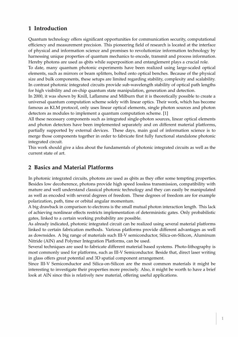
F igure 9: Normalized power of both outputs (red and blue) dependent of th relative phase shift. Deviations fromε = 0.5 induce unbalanced output behaviour [6].
Applying epsilon of 0.5 further simplifies probabilities to sin2(θ/2) and cos2(θ/2). This meansthe output is completely determined by adjusting a certain phase shift θ. Normalized intensitiesof the two outputs as function of relative phase shift for coherent bright-light input (for a couplingratio of ε = 0.3)Two power meter at both outputs can be used for bright-light-intensity detection whereas twoavalanche photodiodes detect single-photons. When this chip is characterized by single-photonsof a SPDC source, it is possible to scan both arms with applied Voltage linearly which resultsin classical interference fringes for bright-light and single photons with the same intensities.Shown in Figure 9, the red and blue normalized dots are related to output 5 and 6. They canbe modulated by changing relative phase at the implemented phase shifter. For this chip, an ε
of roughly 0.3 was chosen instead of 0.5 since it provides much lower losses. Of course, outputintensities are unbalanced due to the deviation from an ε of 0.5.
The same Mach–Zehnder interferometer can be used for two incident photons in input 1 and2. Again, |11〉 as an input state can expressed within the creation operator in both ports:|11〉 = a†
1 a†2 |00〉
|11〉 DC1−−→ [i√
ε(1− ε) (a†3 a†
3 + a†4 a†
4) + (1− 2ε) (a†3 a†
4)] |00〉Phaseshi f t−−−−−→ [i
√ε(1− ε) (a†
3 a†3 + e−i2θ a†
4 a†4) + (1− 2ε)e−iθ a†
3 a†4 |00〉
DC2−−→ i√
2ε(1− ε) [−εe−i2θ + (1− 2ε)e−iθ + (1− ε)] |20〉+
i√
2ε(1− ε) [(1− ε)e−i2θ + (1− 2ε)e−iθ−ε] |02〉+
[−2ε(1− ε)e−i2θ + (1− 2ε)2e−iθ − 2ε(1− ε)] |11〉
(11)
Although this output state is very complex, it is still possible to adjust a certain output state, bymodulating ε. Beside the states where both photons occur at the same output, a mixed state canbe achieved even for ε.
10
∣∣∣∣∣

5 Single Photon Detection with Superconducting Nanowires
Photon detectors are a crucial component according to the KLM scheme. Superconductingnanowires mounted onto waveguides are a good approach for on-chip single photon detection.Recently, GaAs waveguides have been modified with niobium nitride nanowires, shown in Figure10. Such nanowires have ultrahigh sensitivity at telecommunication wavelengths and thus arefeasible for single-photon detection. Additional simulations indicate the fundamental modeelectric field amplitude whereas evanescent field impinges on the nanowire.
F igure 10: Schematic view of a GaAs waveguide equipped with a NbN superconducting nanowire single-photondetector. Simulations show the fundamental mode for light propagation [8].
These nanowires are maintained well below their superconducting temperature as well as criticalcurrent density. The evanescent field of a propagating photon induces a hotspot, which disturbssuperconductivity. It is possible to meassure the induced electrical pulse and therefore photonscan be detected.
6 Future Directions and Summary
So far, all necassary components due to the KLM quantum computation scheme have beenimplemented on single chips of several platforms. All these different materials offer differentadvantages but also suffer from certain drawbacks.Photonic integrated circuits promise significant opportunities and improvements for communica-tion security, computational efficiency and measurement precision.Versatile codeable degrees of freedom such as polarization, path, time or orbital angular momen-tum offer a great potential for future applications and possibilities. Further improvements ofphoto-lithography techniques and especially direct laser writing opens a new window for on-chipelements and their spatial arrangement.Furthermore, new material platforms and their possible implementation of single-photon sources,linear optical elements as well as photon detectors will improve functionality, lead to higher on-chip density and thus higher stability. So far, all necessary components, like photon-sources, linearoptical elements and photon detectors have been implemented on different material platforms.On the way to a fully functional quantum computer, main task is the implementation of photonsources, optical elements and detectors on a single chip.
∣∣∣∣∣ 11

References
[1] E. Knill, R. Laflamme and G.J. Milbrun A scheme for efficient qunatum computation with linearoptics (Nature 409, 46-52, 2001)
[2] M.H. Shih Introduction to Photonic Integrated Circuits (Research Center for Applied Sciences(RCAS) PPT, 2008)
[3] I. Agha Low-noise on-chip frequency conversion by four-wave-mixing Bragg scattering in SiNxwaveguides (Optics Letters 37 (14), 2997-2999, 2012)
[4] X. Guo Parametric down-conversion photon pair source on a nanophotonic chip (arXiv:1603.03726v1,2016)
[5] URL https//www.wikiwand.com/en/Hong–Ou–Mandele f f ect (2015)
[6] J. Wang et al. Gallium arsenide (GaAs) quantum photonic waveguide circuits (Optics Communica-tions 327, 49-55, 2014)
[7] M. Schwartz et al. Generation, guiding and splitting of triggered single photons from a resonantlyexcited quantum dot in a photonic circuit (Optics Express 24 (3), 3089-3094, 2016)
[8] J.P. Sprengers et al. Waveguide superconducting single-photon detectors for integrated quantumphotonic circuits (Applied Physics Letters 99, 181110, 2011)
12
∣∣∣∣∣