silicon electronic photonic integrated circuits (siepic) – research training
TRANSCRIPT

Dr. Lukas ChrostowskiJune 23, 1015
SiEPIC CREATE
Silicon Electronic Photonic Integrated Circuits (SiEPIC) – Research Training

© 2015 L. ChrostowskiSi-EPIC CREATE
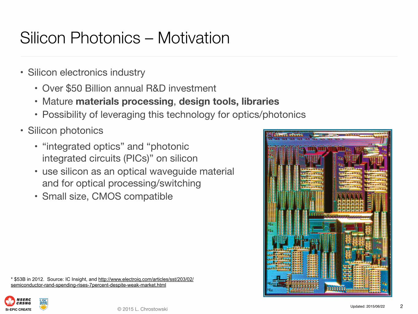
Silicon Photonics – Motivation
• Silicon electronics industry• Over $50 Billion annual R&D investment• Mature materials processing, design tools, libraries• Possibility of leveraging this technology for optics/photonics
2
* $53B in 2012. Source: IC Insight, and http://www.electroiq.com/articles/sst/203/02/semiconductor-rand-spending-rises-7percent-despite-weak-market.html
Updated: 2015/06/22
© 2015 L. ChrostowskiSi-EPIC CREATE
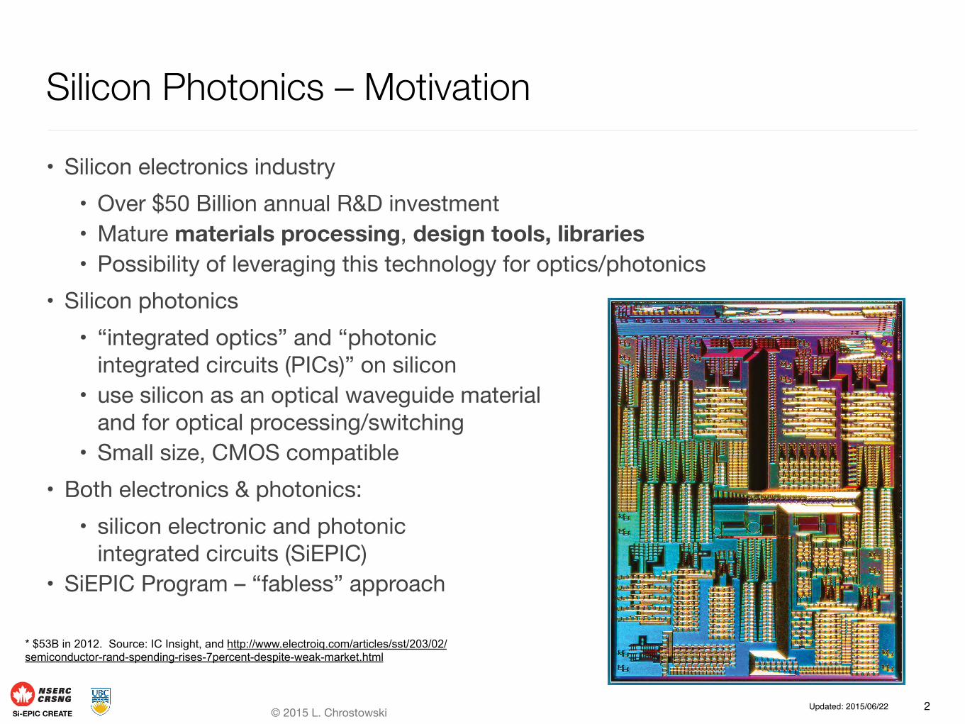
Silicon Photonics – Motivation
• Silicon electronics industry• Over $50 Billion annual R&D investment• Mature materials processing, design tools, libraries• Possibility of leveraging this technology for optics/photonics
• Silicon photonics• “integrated optics” and “photonic
integrated circuits (PICs)” on silicon• use silicon as an optical waveguide material
and for optical processing/switching• Small size, CMOS compatible
2
* $53B in 2012. Source: IC Insight, and http://www.electroiq.com/articles/sst/203/02/semiconductor-rand-spending-rises-7percent-despite-weak-market.html
Updated: 2015/06/22

© 2015 L. ChrostowskiSi-EPIC CREATE
Silicon Photonics – Motivation
• Silicon electronics industry• Over $50 Billion annual R&D investment• Mature materials processing, design tools, libraries• Possibility of leveraging this technology for optics/photonics
• Silicon photonics• “integrated optics” and “photonic
integrated circuits (PICs)” on silicon• use silicon as an optical waveguide material
and for optical processing/switching• Small size, CMOS compatible
• Both electronics & photonics: • silicon electronic and photonic
integrated circuits (SiEPIC)
2
* $53B in 2012. Source: IC Insight, and http://www.electroiq.com/articles/sst/203/02/semiconductor-rand-spending-rises-7percent-despite-weak-market.html
Updated: 2015/06/22
© 2015 L. ChrostowskiSi-EPIC CREATE
Silicon Photonics – Motivation
• Silicon electronics industry• Over $50 Billion annual R&D investment• Mature materials processing, design tools, libraries• Possibility of leveraging this technology for optics/photonics
• Silicon photonics• “integrated optics” and “photonic
integrated circuits (PICs)” on silicon• use silicon as an optical waveguide material
and for optical processing/switching• Small size, CMOS compatible
• Both electronics & photonics: • silicon electronic and photonic
integrated circuits (SiEPIC)• SiEPIC Program – “fabless” approach
2
* $53B in 2012. Source: IC Insight, and http://www.electroiq.com/articles/sst/203/02/semiconductor-rand-spending-rises-7percent-despite-weak-market.html
Updated: 2015/06/22

© 2015 L. ChrostowskiSi-EPIC CREATE
Outline
• SiEPIC workshops• History• Statistics on past workshops• Upcoming 2015 workshops – Actives, CMOS, Systems• Conference short courses at GFP and IPC• Online course edX Silicon Photonics Design, Fabrication and Data Analysis
• Example research results• Keep in touch
3

© 2015 L. ChrostowskiSi-EPIC CREATE
NSERC CREATE – SiEPIC program
• 6-year program announced by NSERC on June 26, 2012• with history going back to 2008.
• The Silicon Electronic-Photonic Integrated Circuits (SiEPIC) Program is an NSERC funded CREATE program designed to train undergraduate and graduate students and postdoctoral fellows across Canada in the new discipline of information and communication technology (ICT) systems that involves miniaturization of optical components onto silicon chips.
• The Program involves the participation of leading researchers from five Canadian Universities, with diverse expertise in silicon photonics:• The University of British Columbia • McGill University • McMaster University • Université de Sherbrooke • University of Ottawa
• Collaborations with Université Laval, University of Toronto, and industries.• http://siepic.ubc.ca/
4

SiEPIC ProgramSi-EPIC CREATE
NSERC CREATE – SiEPIC – Program Objective
• The key objective of the SiEPIC program is to train students to be innovative designers and to enhance their capacity to engage in innovation and commercialization with industry partners. The program has been designed to provide students a wide range of experience through• research projects, • workshops, • industrial internships and • professional development trainings/seminars.
• Our goal is to foster research collaboration among trainees and researchers, enhance student mobility and broaden their experiences for national and international careers in academia, government and industry.
• Design–fabrication–test cycle: students conduct research in modelling, design devices and systems that are fabricated by leading-edge industrial foundries and perform test and measurements. Successful devices will contribute to a SiEPIC Library.
5

Lukas Chrostowski Program Director – SiEPIC Program Associate Professor, Electrical and Computer Engineering University of British Columbia http://www.ece.ubc.ca/faculty/lukas-chrostowski
Vincent Aimez Professor, Electrical and Computer Engineering University of Sherbrooke http://www.usherbrooke.ca/gelecinfo/fr/pers/profs/aimv-fr/
Andrew P. Knights Associate Professor, Engineering Physics McMaster University http://engphys.mcmaster.ca/faculty_staff/faculty/knights/
Wei-Ping Huang Professor, Electrical and Computer Engineering McMaster University http://photonsrvr.ece.mcmaster.ca/huang/Home.htm
Jeff F. Young Professor, Physics and Astronomy University of British Columbia https://www.phas.ubc.ca/users/jeff-young
Nicolas A. F. Jaeger Professor, Electrical and Computer Engineering University of British Columbia http://www.ece.ubc.ca/~nickj/
SiEPIC ProgramSi-EPIC CREATE
SiEPIC Grant – UBC, McGill, McMaster, Ottawa, Sherbrooke
6
Shahriar Mirabbasi Associate Professor, Electrical and Computer Engineering University of British Columbia http://www.ece.ubc.ca/~shahriar/
Odile Liboiron-Ladouceur Assistant Professor, Electrical and Computer Engineering McGill University http://www.photonics.ece.mcgill.ca/Liboiron-Ladouceur/Liboiron-Ladouceur.html
David V. Plant Professor, Electrical and Computer Engineering McGill University http://www.photonics.ece.mcgill.ca/Plant/Plant.html
Jianping Yao Professor and University Research Chair in Microwave Photonics University of Ottawa http://www.site.uottawa.ca/~jpyao/
Robert W. Boyd Professor and Canada Excellence Research Chair, Quantum Physics University of Ottawa http://www.quantumphotonics.uottawa.ca/robert-boyd-en.php

SiEPIC ProgramSi-EPIC CREATE
SiEPIC – Collaborators, Industry
• Collaborators• Joyce Poon, University of Toronto• Sophie Larochelle, Universite Laval• Wei Shi, Universite Laval
• Agencies• CMC Microsystems: development of design kits, instruction at the workshops, technical
support, organizes the workshop-MPW foundry submission, fabrication cost subsidy• C2MI (Centre de Collaboration MiQro Innovation / MiQro Innovation Collaborative Centre),
Bromont, QC: pre-commercialization R&D on packaging the SiEPIC chips• National Research Council, Institute for Microstructural Sciences
• Industry – internships for SiEPIC scholars• TeraXion, Inc.• Lumerical Solutions, Inc.• Crosslight Software, Inc.• Optelian, Versawave Inc.• PMC Sierra, Inc.• Reflex Photonics, Inc.• Telus
7

SiEPIC ProgramSi-EPIC CREATE
SiEPIC – Collaborator – CMC Microsystems
• CMC Microsystems – a non-profit organization, provides industrial microelectronic technologies to Canadian universities, both to facilitate world-class research and to ensure a strong source of well-trained graduates.
• CMC’s roles in the SiEPIC program:• organizes the MPW fabrication runs• subsidizes trainees to attend SiEPIC courses• subsidizes SiEPIC chip fabrication• provides design software• Scientific staff contributes towards the development of design kits,
provides instruction at the workshops, provides technical support for design software, merges the trainees’ designs onto a single submission to the foundry, organizes annual meetings, organizes the scholarship application review process, and provides PDK access.
8
© 2015 CMC Microsystems
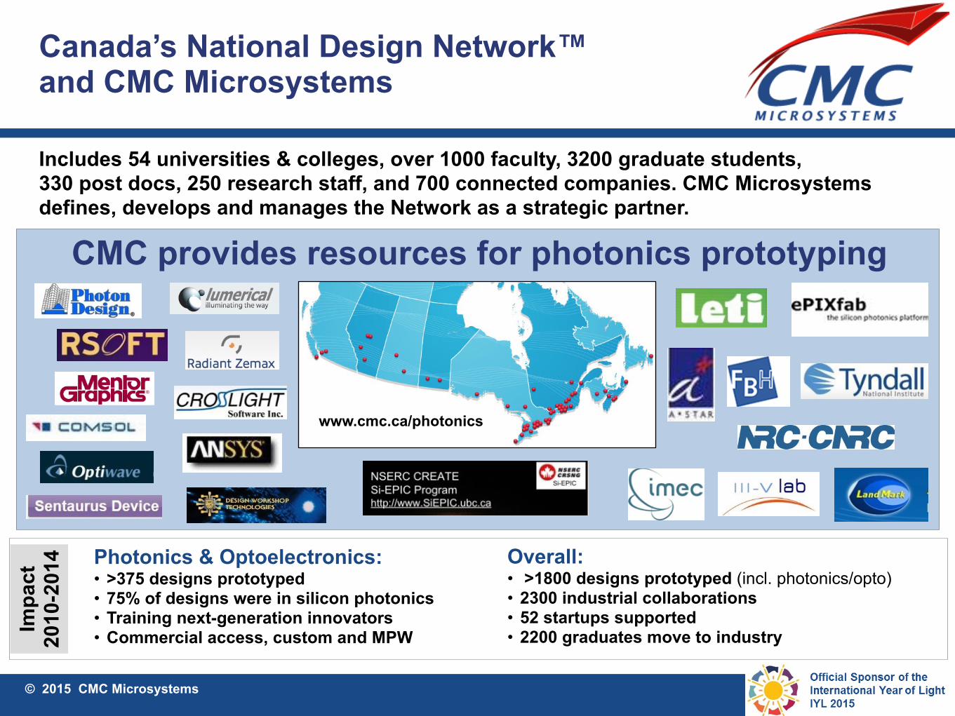
Canada’s National Design Network™and CMC Microsystems
Impa
ct
2010
-201
4
Includes 54 universities & colleges, over 1000 faculty, 3200 graduate students, 330 post docs, 250 research staff, and 700 connected companies. CMC Microsystems defines, develops and manages the Network as a strategic partner.
Photonics & Optoelectronics: • >375 designs prototyped • 75% of designs were in silicon photonics • Training next-generation innovators • Commercial access, custom and MPW
Overall: • >1800 designs prototyped (incl. photonics/opto) • 2300 industrial collaborations • 52 startups supported • 2200 graduates move to industry
CMC provides resources for photonics prototyping
www.cmc.ca/photonics

© 2015 CMC Microsystems
Photonics Designs Progressing to Prototypes
Over 450 photonic/optoelectronic designs fabricated Over 300 of these
designs were silicon photonic technologies
75% of the silicon photonics designs resulted from the Canada-‐wide advanced training program delivered through UBC, in partnership with CMC (now Si-‐EPIC).
(Actual Designs: 467; 2008+)

© 2015 CMC Microsystems
Collaborative cost-sharing R&D projects addressing technology roadmap challenges – 12 active projects; opto highlights include:
• Optical and RF I/O to Si-photonics chips • Lateral fibre array connection to Si-P • Grey-scale photolithography • University-based flip chip service • 2.5D and 3D optoelectronic integration • Microsystem Integration Platform
CMC Solutions www.cmc.ca/cmcsolutions

© 2015 L. ChrostowskiSi-EPIC CREATE
Silicon Electronic-Photonic Integrated Circuits (SiEPIC) Workshops – www.siepic.ubc.ca
• SiEPIC program – 4 annual workshops in:• Passive Photonics – May 2015 at UBC
• Fibre grating couplers, resonators (rings, disks, waveguide Bragg gratings, photonic crystals), splitters (ybranches, directional couplers), optical filters; via IME
• Active Photonics (modulators and detectors) – August 2015 at UBC• PN/PIN junction ring and Mach-Zehnder modulators, detectors; via CMC-IME
• CMOS Electronics for silicon photonics – September 2015 at Concordia• modulator drivers, amplifiers for detectors, optical link analysis; via IBM
• Systems, Integration, Packaging – November 2015 at McGill• CMOS+photonic integration, system-level design and modelling, packaging
• Workshops open to all• Industry and academia
(20+ universities so far)
12Updated: 2015/05/02

© 2015 L. ChrostowskiSi-EPIC CREATE
Workshop Participation – Numbers
• Since 2008, total numbers of …• SiEPIC workshops = 14
• Passives, Actives, CMOS, Systems
• Participants = 273• (218 unique participants)
• Institutions = 41• (26 universities)
• Industry Participants = 23• Supervisors = 53• Most active universities (>10 participants):
• McGill University• University of British Columbia• Université Laval• McMaster University• University of Toronto
13

© 2015 L. ChrostowskiSi-EPIC CREATE
Workshop Participation – Numbers
• On average, 23 per university workshop.
14
© 2015 L. ChrostowskiSi-EPIC CREATE
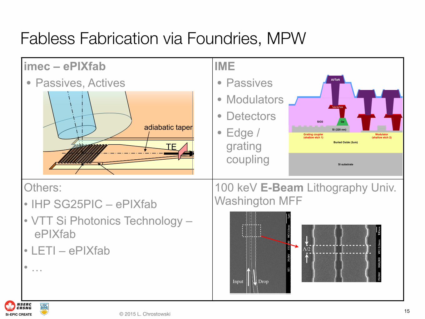
imec – ePIXfab • Passives, Actives
IME • Passives • Modulators • Detectors • Edge /
grating coupling
Others: • IHP SG25PIC – ePIXfab • VTT Si Photonics Technology –
ePIXfab • LETI – ePIXfab • …
100 keV E-Beam Lithography Univ. Washington MFF
Fabless Fabrication via Foundries, MPW
15
Λ/2
DropInput
© intec 2008 - Photonics Research Group - http://photonics.intec.ugent.be
10°
TE
Grating Fiber Coupler
to integrated
circuit
adiabatic taper (>150µm)
10µm wide waveguidegrating
single-mode fibre,
SiEPIC ProgramSi-EPIC CREATE
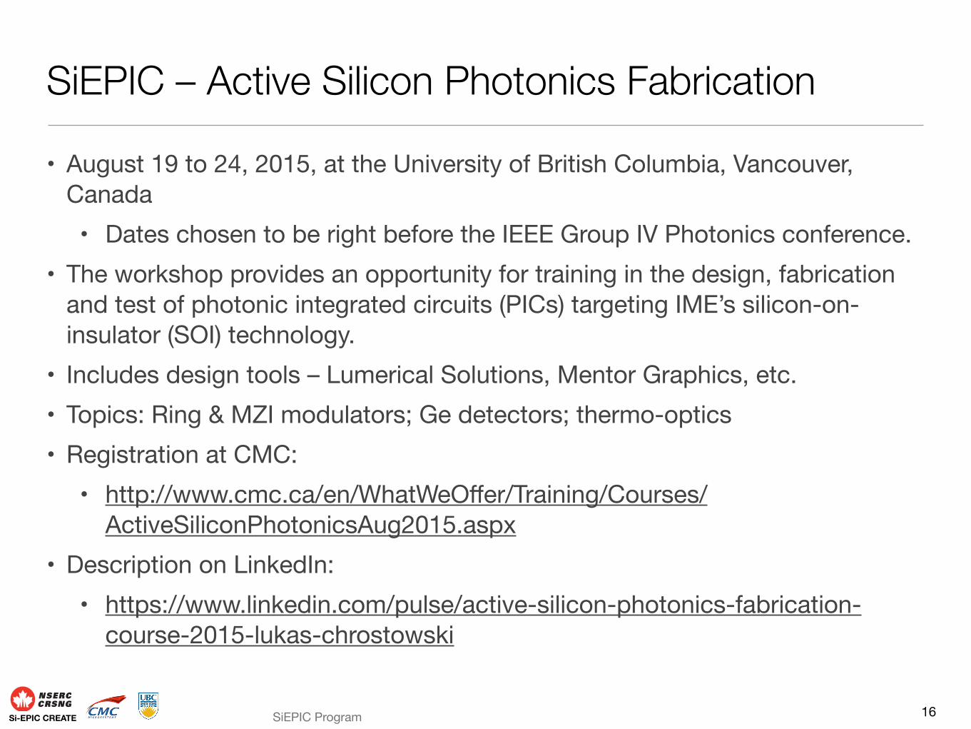
SiEPIC – Active Silicon Photonics Fabrication
• August 19 to 24, 2015, at the University of British Columbia, Vancouver, Canada• Dates chosen to be right before the IEEE Group IV Photonics conference.
• The workshop provides an opportunity for training in the design, fabrication and test of photonic integrated circuits (PICs) targeting IME’s silicon-on-insulator (SOI) technology.
• Includes design tools – Lumerical Solutions, Mentor Graphics, etc.• Topics: Ring & MZI modulators; Ge detectors; thermo-optics• Registration at CMC:
• http://www.cmc.ca/en/WhatWeOffer/Training/Courses/ActiveSiliconPhotonicsAug2015.aspx
• Description on LinkedIn:• https://www.linkedin.com/pulse/active-silicon-photonics-fabrication-
course-2015-lukas-chrostowski
16

© 2015 L. ChrostowskiSi-EPIC CREATE
Workshop schedule – Design cycle
17
Design & Modelling
Mask Layout
Fabrication (Foundry)
Test
Workshop (1 week)
x position [nm]
y p
osi
tion
[n
m]
Electric Field (Ex) in the TE0 polarization
200 400 600 800 1000 1200
200
400
600
800
1000
1200
1400
1600
and is the perturbation period that is chosen to be 330 nm and 290 nm for SW couples and RW couplers,respectively. The intra-waveguide reflection to the input waveguide only happens at its Bragg wavelength,a = 2na. The SW couplers have a height of 220 nm, a coupler gap of 150 nm, and a period number of2000. The RW couplers have a rib height of 70 nm, a slab height of 150 nm, a coupler gap of 900 nm, and aperiod number of 4000. All of the couplers have an input waveguide width, Wa, of 400 nm and an add-dropwaveguide width, Wb, of 500 nm. The corrugation size is controlled to tailor the bandwidth. All of thedevices were fabricated by imec, Belgium accessed via ePIXfab, using 193-nm optical projection lithography.
Shi, Wei ©2011
Design principles of contradirectional couplers
Principle: efficient coupling requires phase match
Suppression of codirectional coupling
Two waveguides with different widths
Contradirecional coupling
Periodic dielectric perturbation between two waveguides
8
indices are calculated using the FDTD mode solutionswith 5 nm meshes.
The transmissionThe
1510 1515 1520 1525 1530!45
!40
!35
!30
!25
!20
!15
Wavelength [nm]
Po
we
r [d
Bm
]
Drop
Through
!a
+ + !
a
! !a
+ + !
b
!
Fig. 2. One-column figure set with the figure environ-ment.
!"#! !"## !"#$ !"#%&
&'!
&'#
&'$
&'%
&'"
&'(
&')
&'*
&'+
!
,-./0/1234 5167
!"#$%&'()*+),&)-.'"/0%1213
!"#! !"## !"#$ !"#%&
&'!
&'#
&'$
&'%
&'"
&'(
&')
&'*
&'+
!
,-./0/1234 5167
89:6-0;</=>/?0/@3;915-'A'7
!"#! !"## !"#$ !"#%&
&'!
&'#
&'$
&'%
&'"
&'(
&')
&'*
&'+
!
,-./0/1234 5167
89:6-0;</=>/?0/@3;915-'A'7
&'$" 16&'(# 16
!')( 16
4%5 465 4-5
Fig. 3. One-column figure set with the figure environ-ment.
Sample code for the preamble is as follows:
\documentclass[10pt,twocolumn]article\usepackageol%% Figures should be placed in body%% of manuscript and%% sized appropriately.
The command \twocolumn[...] must be placedaround the titlepage elements in the two-column option.Note that proper figure, table, and caption environmentsshould be used (see samples below).
Displayed equations may be the most problematicfor two-column display. Optics Letters equations are usu-ally set in one column; breaks and alignment shouldbring out the structure of the math:
=
4
a(x, y) · 1(x, y) b(x, y) dx dy (1)
Photonic bandgap
=22
0
(ng,a + ng,b)| | (2)
= 1 2 m
= 0 (3)
Ex,y =12
(1 + j) (Gx,y )Ex,y
+ Ex,y (t ) exp (jx,y)
+ (spN)1/2x,y. (4)
Ex,y =12
(1 + j) (Gx,y )Ex,y
+ Ex,y (t ) exp (jx,y)
+ (spN)1/2x,y. (5)
Use standard LaTeX or AMSTeX environ-ments. For equations that must span two columns,it is possible to use a float environment, e.g.,\beginfigure*...\endfigure*. Such an en-vironment will not interfere with figure or tablenumbering (which is controlled by the caption), butit will cause equations to float, often with unwantedconsequences.
Figures should be set to one-column size (8.3 cm)whenever possible; tables should also be set to one col-umn whenever possible, but tables with more than fivecolumns will probably need to be set to two columns. Fortwo-column layout, figures and tables can be set acrossboth columns with the alternate figure and table environ-ment commands \beginfigure*...\endfigure*instead of \beginfigure...\endfigure. Note thattables are typeset and cannot be reduced in size like art,which may require more space than in the submittedpaper.
Sample figure environment:\beginfigure[htb]\centerline\includegraphics[width=8.3cm]richardson-f1.eps\captionSample figure.\endfigure
References callouts are now formatted with the citepackage, which produces bracketed reference style (e.g.,[1]). For online callouts, e.g., see [1], the words “Ref.”and “Refs.” are not required.
Before submitting, authors who use BibTeX shouldfirst run BibTeX, then paste the contents of the outputfile *.bbl into the *.tex manuscript file. Our electronicsubmissions system cannot process BibTeX directly.
The following files are included in this distribu-tion:
• OLpagelength.tex Template and instructions• ol2.sty Style file• ol.bst BibTeX style file for short-form citations
(as published)
2
Fig. 1. Schematic of the contradirectional couplers with the fibre grating couplers (FGC).
1470 1480 1490 1500 1510 1520 1530−35
−30
−25
−20
−15
−10
−5
0
Wavelength, nm
Nor
mal
ized
Res
pons
e, d
B
1510 1512 1514 1516 1518−35
−30
−25
−20
−15
−10
−5
0
Wavelength, nm
Nor
mal
ized
Res
pons
e, d
B
1470 1480 1490 1500 1510 1520 1530−35
−30
−25
−20
−15
−10
−5
0
Wavelength, nm
Nor
mal
ized
Res
pons
e, d
B
1510 1512 1514 1516 1518−35
−30
−25
−20
−15
−10
−5
0
Wavelength, nm
Nor
mal
ized
Res
pons
e, d
B
λD
λa
ThroughDrop
500 nm
330 nm 20 nm
150 nm
400 nm
500 nm
(a) (b)
Fig. 2. A sidewall-modulated SW contradirectional coupler: (a) SEM image of the sidewall-modulated stripwaveguides; (b) through-port and drop-port spectra with the inset showing the zoomed-in spectra at D.
(a) (b)
1514 1516 1518 1520 1522 1524 1526 1528
−30
−25
−20
−15
−10
−5
0
Wavelength, nm
Nor
mal
ized
Res
pons
e, d
B
CMC2R0C1CDCRib7T
ThroughDrop
λD
λa
500 nm5 µm
400 nm 500 nm290 nm
Input
Drop
Fig. 3. An RW contradirectional coupler: (a) SEM image of the coupler with the inset showing the tiltedcross-section; (b) through-port and drop-port spectra.
3. Results and Discussion
The through-port and drop-port spectra of a sidewall-modulated SW contradirectional coupler and an RWcontradirectional coupler are shown in Fig. 2 (b) and Fig. 3 (b), respectively. The SW coupler has a widespacing of approximately 38 nm between a and D, which is desirable for C-band WDM applications. TheRW coupler has a narrower spacing between a and D due to the smaller di↵erence between na and nb.However, this spacing can be increased by varying the waveguide widths, allowing for WDM applications
2
1476.85 1476.95 1477.05 1477.15−20
−18
−16
−14
−12
−10
−8
−6
−4
−2
0
Wavelength (nm)
Tran
smis
sion
(dB)
~15 pm
Q: ~100,000
peak, λ0D, is extended to over 30 nm, applicable to state-of-the-art DWDM (dense WDM) systems.
The drop-port spectrum is calculated using coupled-mode theory [4], with the reflectivity (i.e., the contradir-ectional coupling efficiency) given by
η ¼ jκj2 sinh2ðsLÞs2 cosh2ðsLÞ þ ðΔβ=2Þ2 sinh2ðsLÞ ; ð1Þ
where Δβ ¼ βþa − β−b − 2π=Λ and s2 ¼ jκj2 − ðΔβ=2Þ2 [4].The coupling coefficient, κ, is a function of the mode dis-tributions and the dielectric perturbation. It is noticedthat the actual corrugation profile is not rectangular, asin the original design, due to the pattern-size effect in theplasma etching, as is clearly seen in the SEM image inFig. 4. This effect causes weaker coupling strength andthus a narrower bandwidth [5] and has been consideredin our comparison between the simulation and the ex-perimental results. In this Letter, we use a triangularshape to approximate the transverse distribution of thedielectric perturbation (as marked on the SEM imagein Fig. 4) with a linear transition between the perturba-tion peak, Δεp, and the unperturbed section in the long-itudinal direction. Then the dielectric perturbation can beexpressed as
Δεðx; y; zÞ ¼ SðzÞΔεpðx; yÞ: ð2Þ
As shown in Fig. 4, the periodic function SðzÞ describesthe longitudinal distribution of the perturbation. Now κcan be calculated by
Fig. 2. (Color online) Calculated effective indices of thefundamental TE-like modes of the rib waveguides. n0
b and λ0bare the effective-index and the Bragg wavelength, respectively,for Wb ¼ 1 μm.
1510 1512 1514 1516 1518 1520 1522 1524 1526 1528 1530
-40
-35
-30
-25
-20
-15
Wavelength [nm]
Pow
er [d
Bm] Drop
Through
1522 1522.5 15230
0.2
0.4
0.6
0.8
1
Wavelength [nm]
Nor
mal
ized
Ref
lect
ion
[a.u
.]
Experiment
Simulation
λa
λD
Fig. 3. (Color online) Measured spectra of a device with½D;G& ¼ ½220nm; 1 μm&. The input power is 1mW with an inser-tion loss of ∼17dB due to the fiber-coupling to the FGCs. Theinset shows the zoomed-in drop-port spectrum and the simu-lated results.
Fig. 4. (Color online) Dielectric perturbation distributionalong the longitudinal direction. The inset is the SEM imageof the tilted cross-section of a device.
Fig. 1. (Color online) Contradirectional couplers in SOI ribwaveguides: (a) cross-sectional geometry with the calculatedintensity distributions of the fundamental TE-like modes of therib waveguides; (b) top view of the device geometry; (c) SEMimage showing the parabolically broadening transition from thephotonic wires to the rib waveguides; (d) SEM image showingthe corrugations of a device with the propagation constantslabeled and the directions of propagation indicated.
4000 OPTICS LETTERS / Vol. 36, No. 20 / October 15, 2011
Students submit: § Proposal § Design doc
Students submit: § Draft GDS § Final GDS
Students submit: § Final report
Updated: 2014/05/20
SiEPIC ProgramSi-EPIC CREATE
SiEPIC Systems, Integration, Packaging
• November 2-6, 2015 at McGill• Motivation:
• Silicon photonics is rapidly transitioning towards delivering systems built based on mature components. This workshop will stimulate the participants to design silicon photonic systems using components designed and tested in the other SiEPIC workshops. Building a system requires an understanding of integration approaches, both within the chip and with outside components, as well as packaging to connect to the outside world.
• Participants will be guided through challenging system design problems, namely on the topics of:• Optical interconnects – towards 10 Tb/s MZI & Ring transceivers• Sensors – microfluidic evanescent field, for biomedical applications• Microwave photonics• Opto-electronic circuits – what can you do better with both photonics & electronics,
than you can do only with one? • Nano-opto-mechanical systems
• During the next 12 months, teams will work on implementing and testing the chosen system.
18

© 2015 L. ChrostowskiSi-EPIC CREATE
SiEPIC Short Courses
Using Electron Beam Lithography:
•Introduc:on to Silicon Photonics Device Design and Fabrica:on IEEE Photonics Conference – October, 2014 – 3 hours # Par:cipants = 89
•Silicon Photonics Workshop IEEE Group IV Photonics Conference – August 25, 2015 – 3 hours
•Silicon Photonics Fabrica:on Workshop on Sub-‐wavelength Gra:ng Materials / Meta-‐materials IEEE Photonics Conference – October 4, 2015 – 3 hours
•Silicon Photonics Design, Fabrica:on and Data Analysis - UBCx edX Workshop Registra:on – online course: July 7 – August 18, 2015
19
© 2015 L. ChrostowskiSi-EPIC CREATE
Si-EPIC
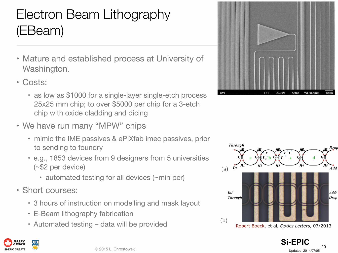
Electron Beam Lithography (EBeam)
• Mature and established process at University of Washington.
• Costs:• as low as $1000 for a single-layer single-etch process
25x25 mm chip; to over $5000 per chip for a 3-etch chip with oxide cladding and dicing
• We have run many “MPW” chips• mimic the IME passives & ePIXfab imec passives, prior
to sending to foundry• e.g., 1853 devices from 9 designers from 5 universities
(~$2 per device)• automated testing for all devices (~min per)
• Short courses:• 3 hours of instruction on modelling and mask layout• E-Beam lithography fabrication• Automated testing – data will be provided
20
Thermally Tunable Quadruple Vernier Racetrack Resonators
Robert Boeck,
Lukas Chrostowski, and Nicolas A. F. Jaeger
Department of Electrical and Computer Engineering, University of British Columbia,2332 Main Mall, Vancouver, BC V6T 1Z4, Canada
Corresponding author: [email protected]
Compiled May 17, 2013
Series-coupled racetrack resonators exhibiting the Vernier e↵ect have many attractive features as comparedto the spectral response of identical racetrack resonators such as free spectral range extension and enhancedwavelength tunability. Here we present experimental results of a thermally tunable quadruple series-coupledsilicon racetrack resonator exhibiting the Vernier e↵ect. We thermally tune two of the four racetrack resonatorsto enable discrete switching of the major peak by 15.54 nm. Also, our device had an interstitial peak suppressionof 35.4 dB, a 3 dB bandwidth of 0.45 nm and an extended free spectral range of 37.66 nm.
c 2013 Optical Society of America
OCIS codes: 230.4555, 250.5300.
Identical series-coupled ring resonators [1,2] have beenfabricated in which each resonator has been thermallytuned. Thermal tuning is desirable since its e↵ect on thee↵ective index is large [3] and there is no excess loss ver-sus current [4]. An increase in temperature tends to shiftthe resonant wavelength by approximately 0.07 nm/oC.To tune the resonant wavelength by the span of the C-band (35.09 nm) would require a temperature change inexcess of 501oC (assuming the thermo-optic coecientis dn/dT = 1.8610-4K-1 [5]). Fortunately, the Verniere↵ect enables one to significantly enhance the resonantwavelength switching range as compared to the range ca-pable when using identical ring resonators [6]. Thermallytunable series [7, 8] and cascaded [6, 10] coupled doublering resonator filters exhibiting the Vernier e↵ect havebeen achieved previously. However, these devices showunacceptable spectral characteristics for typical densewavelength-division multiplexing (DWDM) applicationssuch as low interstitial peak suppression (IPS) [6, 7],small extension of the free spectral range (FSR) [7, 8],no extension of the FSR in the through port [6, 10],and many do not use the silicon-on-insulator (SOI) plat-form [8,10]. Our previous results using double racetrackresonators showed an IPS of 25.5 dB and a 3 dB band-width (BW) of 0.09 nm [9]. However, it is desirableto have a larger IPS and a larger BW. Previously, ithas been theoretically shown that more than two seri-ally coupled ring resonators are needed to achieve su-cient IPS [11–13] while maintaining a large enough BW.Here we experimentally demonstrate the first thermallytunable quadruple series-coupled racetrack resonator ex-hibiting the Vernier e↵ect using SOI strip waveguides.We shift the major peak by 15.54 nm by heating twoof the four racetrack resonators (resonators c and d inFig. 1(a)).
For the modeling and analysis of our quadruple series-coupled racetrack resonator exhibiting the Vernier ef-fect, we have used SOI strip waveguides with heights of220 nm and widths of 502 nm, as well as a top SiO
2
cladding. The Si refractive index is wavelength depen-dent and can be fitted to experimental data using aLorentz model [16]. Since the wavelength dependency ofthe refractive index of SiO
2
is minimal, we have assumeda constant value of 1.4435. Also, we have used 2.4 dB/cmpropagation loss in our modeling. This is consistent withthe value of 2.35±0.33 dB/cm recently reported by [17],for SOI strip waveguides with top SiO
2
claddings. Theschematic of the quadruple Vernier racetrack resonatoris shown in Fig. 1(a), which has an asymmetric arrange-ment of resonators as described in [11–13]. The fabri-cated device is shown in Fig. 1(b).
(a)
! ! ! ! !!
-jκ2
t5 t4 t3 t2 t 1
r r L Lx
Lx t1
In
Through
g1 g2$ g3$ g4$ g5$Add
Drop
a b c d
-jκ1 -jκ3 -jκ4 -jκ5
(b)
In/
Through
Add/
Drop
Fig. 1. (Color online) (a) shows the schematic of thequadruple Vernier racetrack resonator and (b) shows thefabricated device.
La,b,c,d
are the total lengths of the racetrack res-onators,
1
and 5
are the symmetric (real) point fieldcoupling factors to the bus waveguides,
2,3,4
are theinter-ring symmetric (real) point field coupling factors,and t
1,2,3,4,5
are the respective (real) point field trans-mission factors. The following simulations assume thatLa
= Lb
= 2r+2Lx
, where r = 5 µm and Lx
= 7 µm,Lc
= Ld
= (4/3)La
= 2r+2Lx
+2L, where L = 7.569µm,
1
= 5
, 2
= 4
, t1
= t5
, and t2
= t4
. The e↵ectiveindex and field coupling and field transmission factors
1
Robert Boeck, et al, Optics Letters, 07/2013
Updated: 2014/07/05

© 2014 L. Chrostowski
• Automated die-level test for end-users:• 1-2 min per device (50,000 points spectrum)• Parts list ~ $10-20k
• included – nano-steppers, fibre array, microscope; not included – laser/detectors
• Software in Matlab & Python – “Open Source”• Lab Tour: http://bit.ly/SiPlab• Contact CMC for distribution
21
PLCC Coupling Components
Angle Polished Fiber Arrays PLC Fan-in mode field reducers
PLC Angle-Polished PLCs
127 µm Pitch Fiber Array

© 2015 CMC Microsystems
MIP for Si-photonic HW-in-the-loop
Keysight C band tunable laser
Keysight 4 port optical power meter
Custom Micronix auto-
alignment system PLC
Connections 8-element PM
fibre coupler for surface gratingsStandard chip to
verify optical coupling
Silicon Photonics Fabrication – Electron Beam LithographySi-EPIC CREATE
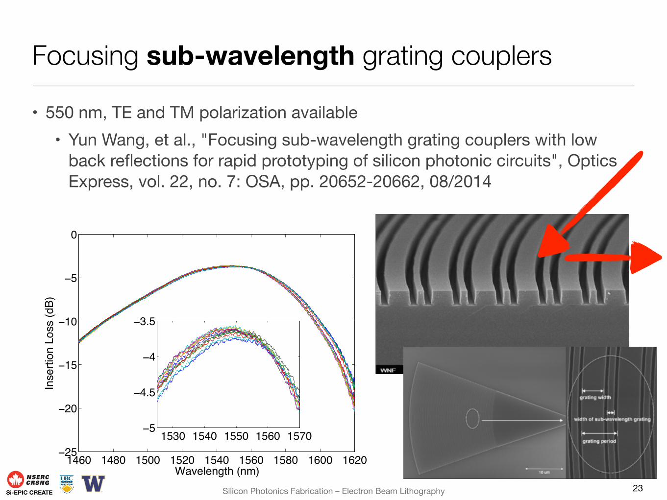
Focusing sub-wavelength grating couplers
• 550 nm, TE and TM polarization available• Yun Wang, et al., "Focusing sub-wavelength grating couplers with low
back reflections for rapid prototyping of silicon photonic circuits", Optics Express, vol. 22, no. 7: OSA, pp. 20652-20662, 08/2014
1460 1480 1500 1520 1540 1560 1580 1600 1620−25
−20
−15
−10
−5
0
Wavelength (nm)
Inse
rtion
Los
s (d
B)
1530 1540 1550 1560 1570−5
−4.5
−4
−3.5
23
Silicon Photonics Fabrication – Electron Beam LithographySi-EPIC CREATE
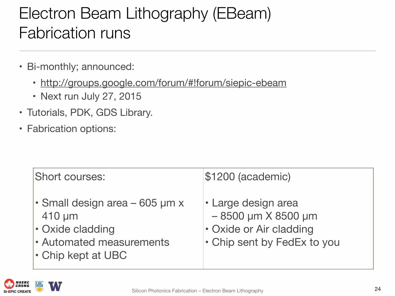
Electron Beam Lithography (EBeam) Fabrication runs
• Bi-monthly; announced:• http://groups.google.com/forum/#!forum/siepic-ebeam• Next run July 27, 2015
• Tutorials, PDK, GDS Library.• Fabrication options:
24
Short courses:
• Small design area – 605 µm x 410 µm
• Oxide cladding• Automated measurements• Chip kept at UBC
$1200 (academic)
• Large design area – 8500 µm X 8500 µm
• Oxide or Air cladding• Chip sent by FedEx to you

© 2015 L. ChrostowskiSi-EPIC CREATE
edX Silicon Photonics Design, Fabrication and Data Analysis
• Question – is possible to scale up the SiEPIC workshops, to make them accessible to anyone in the world• without travel, without test equipment
• Solution:• An online interactive course hosted by edX. It includes lectures, tutorials, activities, a
design review, and part of a textbook. • Fabrication using electron beam lithography. Cost sharing.• Design software from Lumerical Solutions (MODE and INTERCONNECT), Mentor
Graphics (software accessible in the cloud), and MATLAB.• Automated probe stations at The University of British Columbia• And the whole course is only 6 weeks long!
• Philosophy: participant should (quickly) see the complete design cycle first. Once familiar with the tools, techniques, challenges, and opportunities, the participant will be in a much stronger position to dedicate more time for a complex design.
25

© 2015 L. ChrostowskiSi-EPIC CREATE
edX course – Resources – Design tools
• Many tools available
• Commercial tools provided by Lumerical Solutions, Mentor Graphics, Mathworks
• Flexibility in how much time you want to spend on this course
26
Component models
MATLAB Lumerical MODE
Circuit models
MATLAB Lumerical INTERCONNECT
Layout
Pyxis LayoutKLayout
Measurement Data Analysis
MATLAB Python

© 2015 L. ChrostowskiSi-EPIC CREATE
edX course – Design Cycle – Schedule
2727
Modelling & Design
Mask Layout
FabricationAutomated Test
Updated: 2015/05/31
Data Analysis

© 2015 L. ChrostowskiSi-EPIC CREATE
edX course – Design Cycle – Schedule
2727
Modelling & Design
Mask Layout
FabricationAutomated Test
x position [nm]
y posi
tion [nm
]
Electric Field (Ex) in the TE0 polarization
200 400 600 800 1000 1200
200
400
600
800
1000
1200
1400
1600
Updated: 2015/05/31
Data Analysis
Week 1
Week 2
Design Review
Week 3

© 2015 L. ChrostowskiSi-EPIC CREATE
edX course – Design Cycle – Schedule
2727
Modelling & Design
Mask Layout
FabricationAutomated Test
x position [nm]
y posi
tion [nm
]
Electric Field (Ex) in the TE0 polarization
200 400 600 800 1000 1200
200
400
600
800
1000
1200
1400
1600
Final deadline – July 27
Updated: 2015/05/31
Data Analysis
• at UW
Week 1
Week 2
Design Review
Week 3
Week 4

© 2015 L. ChrostowskiSi-EPIC CREATE
edX course – Design Cycle – Schedule
2727
Modelling & Design
Mask Layout
FabricationAutomated Test
x position [nm]
y posi
tion [nm
]
Electric Field (Ex) in the TE0 polarization
200 400 600 800 1000 1200
200
400
600
800
1000
1200
1400
1600
Final deadline – July 27
• at UBCUpdated: 2015/05/31
Data Analysis
• at UW
Week 1
Week 2
Design Review
Week 3
Week 4Week 5
Week 6

© 2015 L. ChrostowskiSi-EPIC CREATE
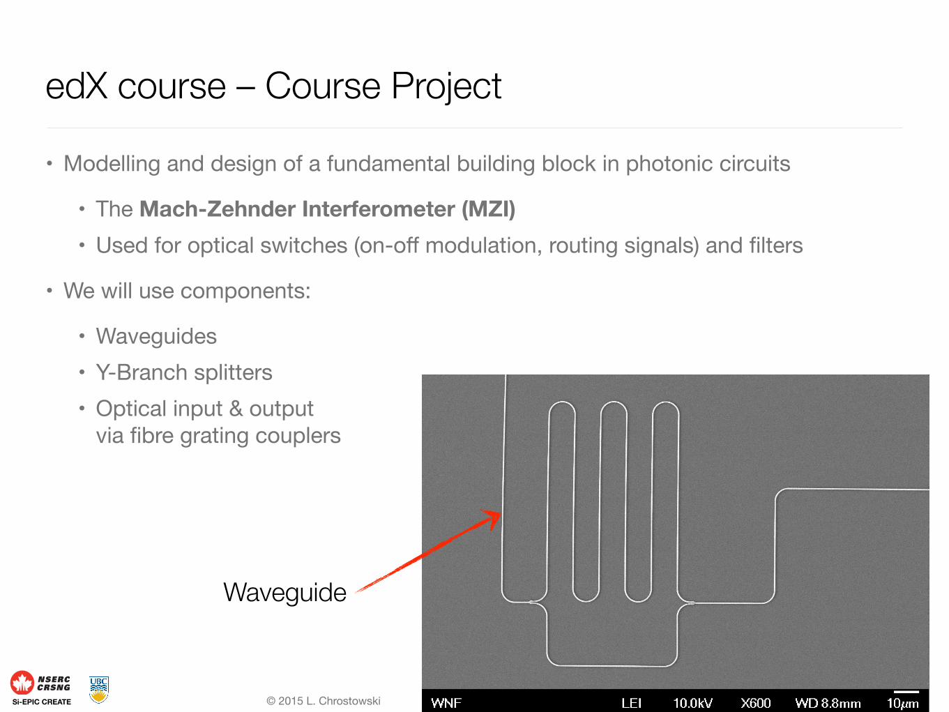
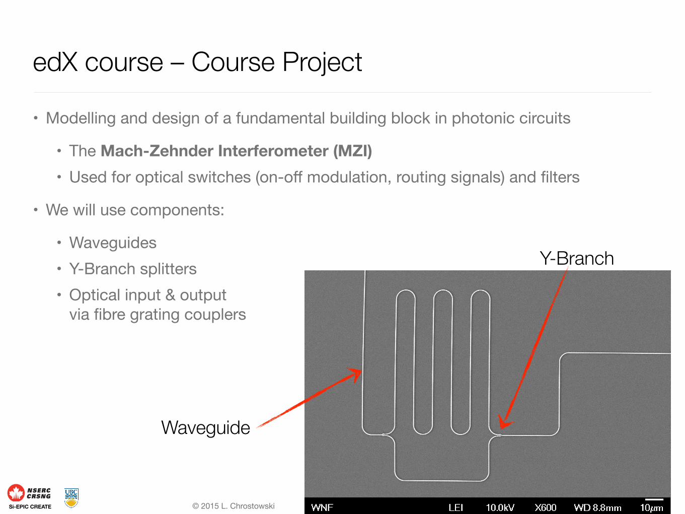
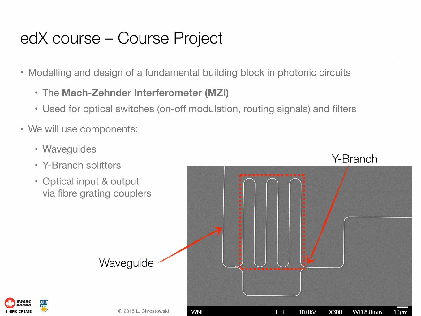
edX course – Course Project
• Modelling and design of a fundamental building block in photonic circuits
• The Mach-Zehnder Interferometer (MZI)• Used for optical switches (on-off modulation, routing signals) and filters
28

© 2015 L. ChrostowskiSi-EPIC CREATE
edX course – Course Project
• Modelling and design of a fundamental building block in photonic circuits
• The Mach-Zehnder Interferometer (MZI)• Used for optical switches (on-off modulation, routing signals) and filters
• We will use components:
• Waveguides• Y-Branch splitters• Optical input & output
via fibre grating couplers
28
Waveguide
© 2015 L. ChrostowskiSi-EPIC CREATE
edX course – Course Project
• Modelling and design of a fundamental building block in photonic circuits
• The Mach-Zehnder Interferometer (MZI)• Used for optical switches (on-off modulation, routing signals) and filters
• We will use components:
• Waveguides• Y-Branch splitters• Optical input & output
via fibre grating couplers
28
Y-Branch
Waveguide

© 2015 L. ChrostowskiSi-EPIC CREATE
edX course – Interference
• Task – Design an imbalanced interferometer, in order to observe constructive and destructive interference
• As a function of wavelength, observe oscillations:
29

© 2015 L. ChrostowskiSi-EPIC CREATE
edX course – Interference
• Task – Design an imbalanced interferometer, in order to observe constructive and destructive interference
• As a function of wavelength, observe oscillations:
29
Constructive Interference

© 2015 L. ChrostowskiSi-EPIC CREATE
edX course – Interference
• Task – Design an imbalanced interferometer, in order to observe constructive and destructive interference
• As a function of wavelength, observe oscillations:
29
Constructive Interference
Destructive Interference

© 2015 L. ChrostowskiSi-EPIC CREATE
Why choose to design an MZI in the edX course?
30

© 2015 L. ChrostowskiSi-EPIC CREATE
Why choose to design an MZI in the edX course?
• Simple to model and design:
• Interferometer – simple equations describing the interference of light
• Single-mode waveguide – numerical calculations to find the speed of light
30

© 2015 L. ChrostowskiSi-EPIC CREATE
Why choose to design an MZI in the edX course?
• Simple to model and design:
• Interferometer – simple equations describing the interference of light
• Single-mode waveguide – numerical calculations to find the speed of light
• Simple for experimentation:
• Easy to create a layout• Automated measurements of your circuit at many wavelength points
• Compare experiments vs. simulations:
• Extract waveguide parameters from experimental data• Get insight into the “real-world” and how manufacturing affects your circuit
performance
• This first experience exposes you to the tools and techniques used to design more complicated devices and systems
30

© 2015 L. ChrostowskiSi-EPIC CREATE
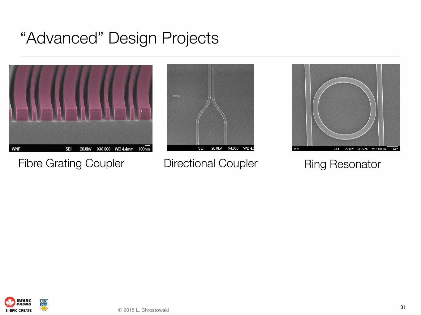
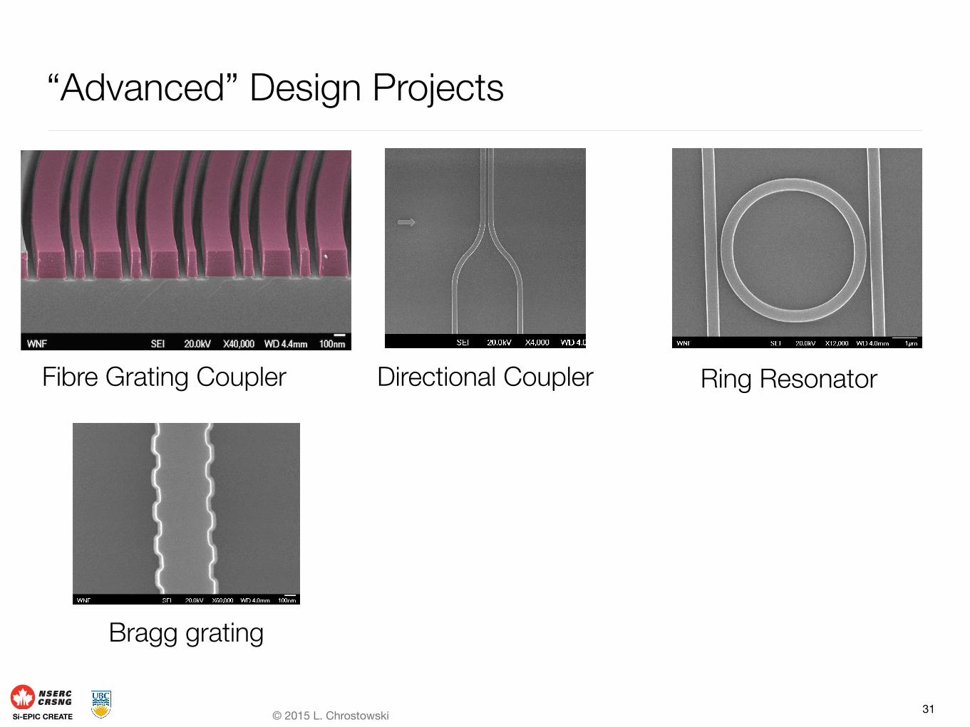
“Advanced” Design Projects
31

© 2015 L. ChrostowskiSi-EPIC CREATE
“Advanced” Design Projects
31
Fibre Grating Coupler

© 2015 L. ChrostowskiSi-EPIC CREATE
“Advanced” Design Projects
31
Fibre Grating Coupler Directional Coupler
© 2015 L. ChrostowskiSi-EPIC CREATE
“Advanced” Design Projects
31
Fibre Grating Coupler Ring ResonatorDirectional Coupler
© 2015 L. ChrostowskiSi-EPIC CREATE
“Advanced” Design Projects
31
Fibre Grating Coupler Ring ResonatorDirectional Coupler
Bragg grating

© 2015 L. ChrostowskiSi-EPIC CREATE
“Advanced” Design Projects
31
Fibre Grating Coupler Ring ResonatorDirectional Coupler
Sub-wavelength structures
Bragg grating

© 2015 L. ChrostowskiSi-EPIC CREATE
“Advanced” Design Projects
31
Fibre Grating Coupler Ring ResonatorDirectional Coupler
Sub-wavelength structures Splitters, MMIsBragg grating

© 2015 L. ChrostowskiSi-EPIC CREATE
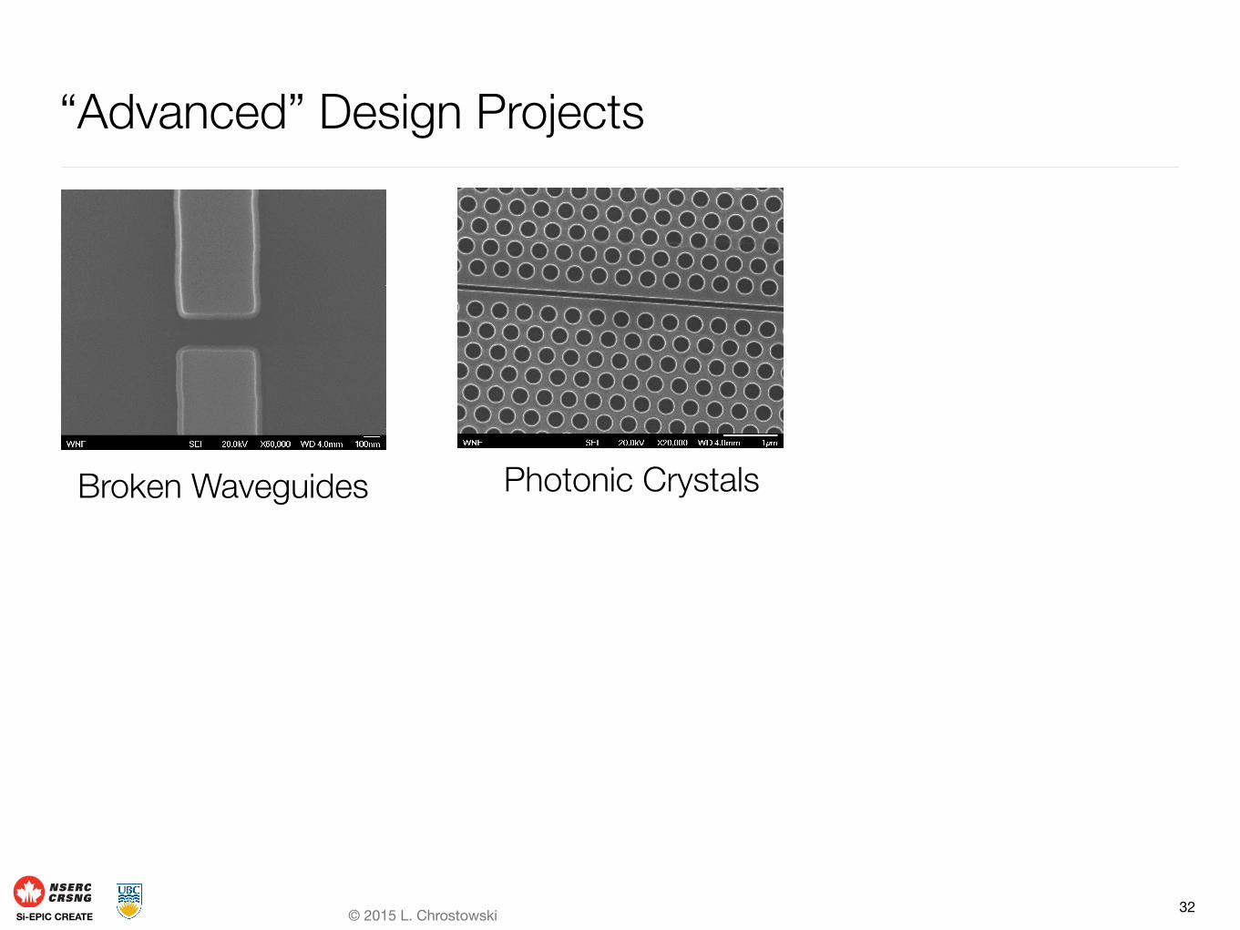
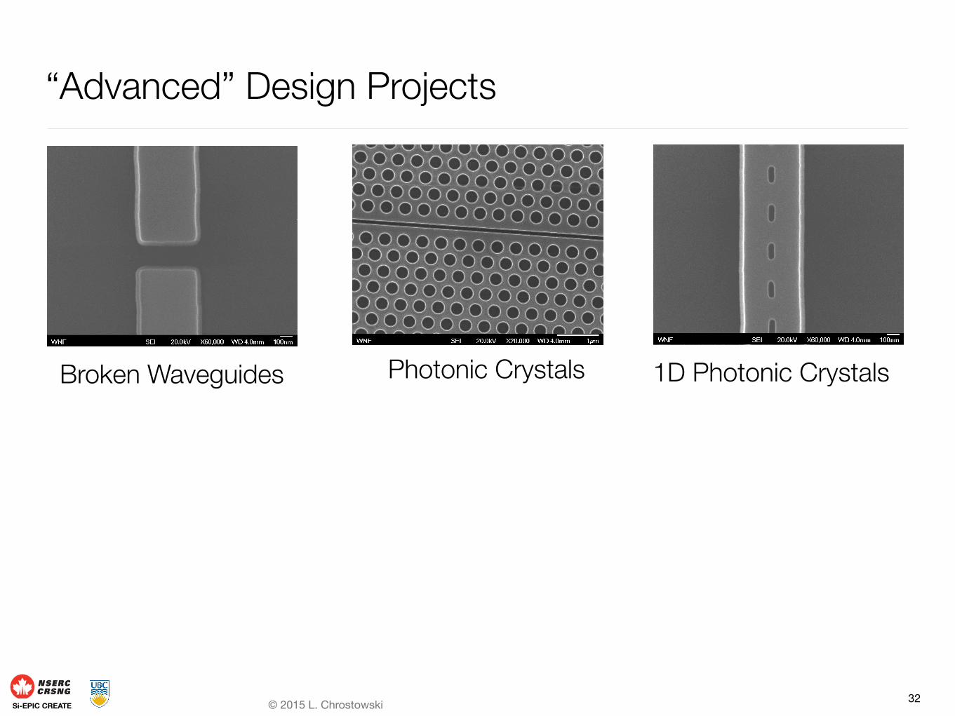
“Advanced” Design Projects
32

© 2015 L. ChrostowskiSi-EPIC CREATE
“Advanced” Design Projects
32
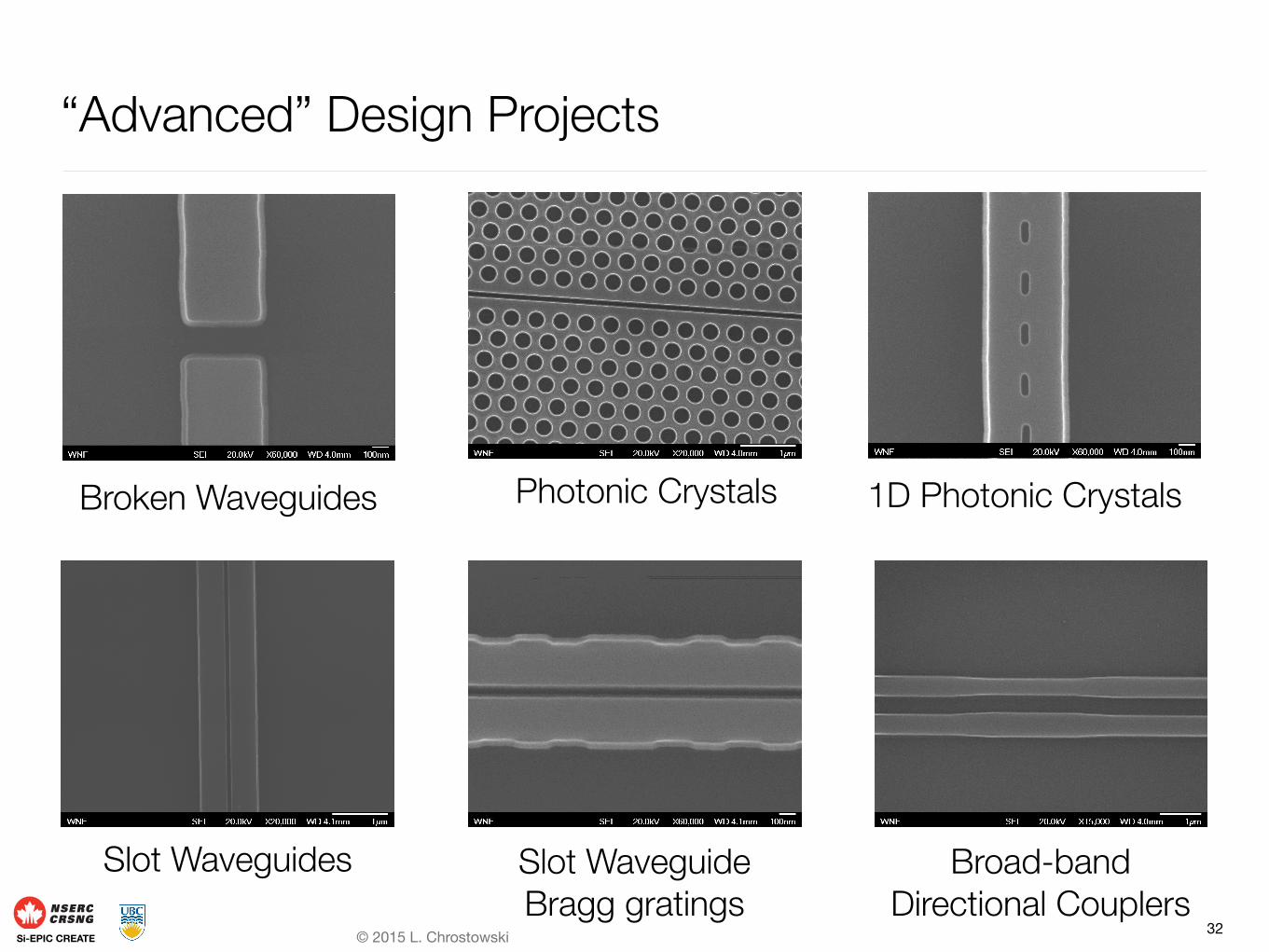
Broken Waveguides
© 2015 L. ChrostowskiSi-EPIC CREATE
“Advanced” Design Projects
32
Photonic CrystalsBroken Waveguides
© 2015 L. ChrostowskiSi-EPIC CREATE
“Advanced” Design Projects
32
Photonic CrystalsBroken Waveguides 1D Photonic Crystals

© 2015 L. ChrostowskiSi-EPIC CREATE
“Advanced” Design Projects
32
Photonic Crystals
Slot Waveguides
Broken Waveguides 1D Photonic Crystals
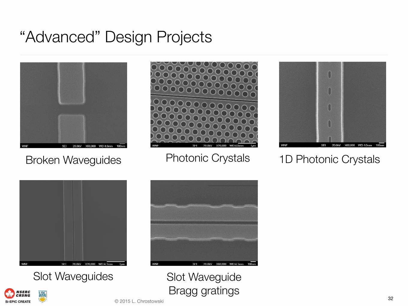
© 2015 L. ChrostowskiSi-EPIC CREATE
“Advanced” Design Projects
32
Photonic Crystals
Slot Waveguides
Broken Waveguides 1D Photonic Crystals
Slot Waveguide Bragg gratings
© 2015 L. ChrostowskiSi-EPIC CREATE
“Advanced” Design Projects
32
Photonic Crystals
Slot Waveguides Broad-band Directional Couplers
Broken Waveguides 1D Photonic Crystals
Slot Waveguide Bragg gratings

© 2015 L. ChrostowskiSi-EPIC CREATE
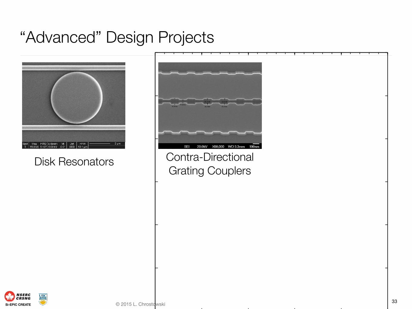
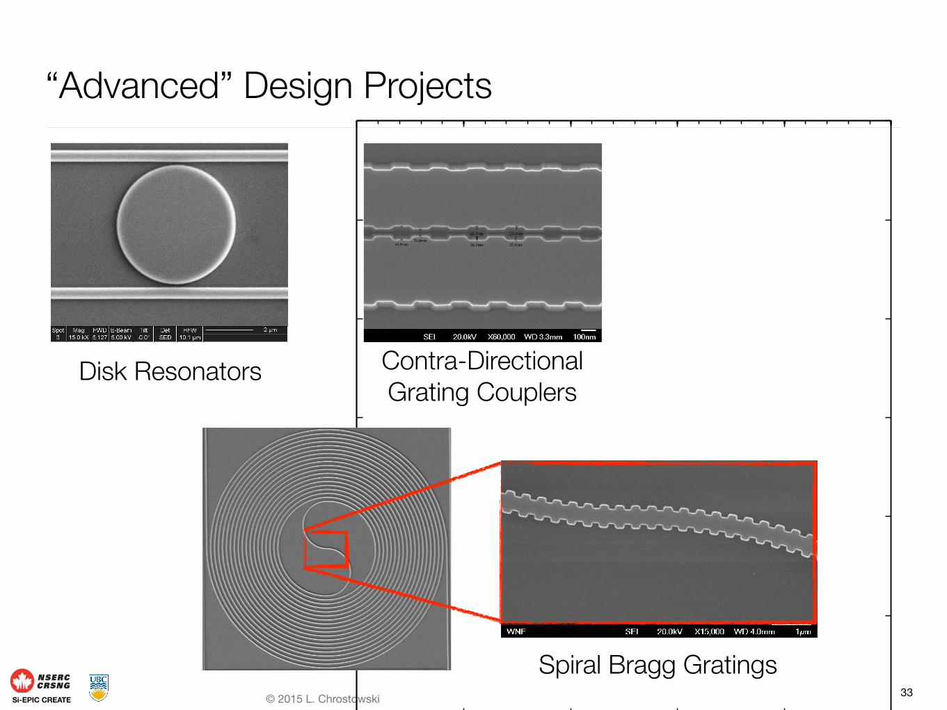
“Advanced” Design Projects
33

© 2015 L. ChrostowskiSi-EPIC CREATE
“Advanced” Design Projects
33
Disk Resonators
a)1470 1475 1480 14850
0.1
0.2
0.3
0.4
0.5
0.6
0.7
0.8
0.9
Wavelength (nm)
Tran
smis
sion
~10 nm
b)1476.85 1476.95 1477.05 1477.15−20
−18
−16
−14
−12
−10
−8
−6
−4
−2
0
Wavelength (nm)
Tran
smis
sion
(dB)
~15 pm
c)Figure 5. a) Measured transmission spectrum of the quarter-wave phase-shifted gratings, (b) enlarged plot around the transmissionresonance, c) SEM image of the fabricated device, showing the quarter-shifted section.
The disk is excited by several dipole sources placed inside the disk. In order to find the sensitivity, we perform severalFDTD simulations with a variation of cladding index of refraction. We then inspect the spectrum of the cavity and observethe shift in the cavity modes (nm), versus the applied changes in refractive index (RIU).
a) b) c)Figure 6. a) 3D FDTD calculation showing the top-view TE mode profile of a 2.5 µm disk. Counting the number of nodes (48) indicatesthat this is mode #24. b) SEM image of the disk. c) Mode calculation for the cross-section of the disk, TE mode (top), TM mode(bottom). All simulation plots are for the E-field intensity.
The second approach is similar to a conventional waveguide mode calculation,50 where we calculate the disk’s cross-section mode profile, effective index, group index and loss for the lowest order TE and TM modes as a function of wave-length. The radius of the disk is included in the simulation by defining the bend radius as the actual radius of the disk.The advantage of this approach is that a much finer mesh can be employed since it is a 2D simulation, hence the accuracycan be improved. Similar to the 3D FDTD simulations, we vary the cladding index and record the shift in effective index.Next, we calculate the resonant modes by using simple Fabry-Perot theory, namely we find solutions where the round-tripphase is an integer multiple of 2, using 2M = 2neff()L/, where L = 2r is the circumference of the disk. Were-write this as
M
2r= neff() (6)
and plot the results of the left-hand-side and right-hand-side of the equation in Figure 7a. The intersection of the neff()line with the mode number lines provides the solution(s) to the equation and yields the resonant wavelength(s). Thistechnique can further be used to find the modes of different sized disks by recalculating the neff versus wavelength graphsand re-plotting the above.
The loss of the each mode is also calculated by the mode solver, including the water absorption. For TM modes, the
8
Contra-Directional Grating Couplers
1460
1490
1520
1550
1580
1610
1640
−25
−20
−15
−10
−5 0
Wav
eleng
th, n
m
Normalized Transmission, dB
λa
λD
20 nm
14
60
14
90
15
20
15
50
15
80
16
10
16
40
−2
5
−2
0
−1
5
−1
0
−5 0
Wav
elength
, nm
Normalized Tran smission, dB
λD
6.5
nm
1460
1490
1520
1550
1580
1610
1640
−25
−20
−15
−10
−5 0
Wav
elength
, nm
Normalized Transmission, dB
λa
λD
20 nm
1460
1490
1520
1550
1580
1610
1640
−25
−20
−15
−10
−5 0
Wav
eleng
th, n
m
Normalized Tran smission, dB
λD
6.5
nm
(a)(b
)
Figure5.(a)Measuredthrough-portspectrum
ofaconventionalcontra-DC
withgratingsbetweenthetwowaveguides;(b)
Measuredthrough-portspectrum
ofananti-reflectioncontra-DC
without-of-phasegratingstosuppressbackreflections.
Insets:SEM
images.
investigated.
To
overcome
this
issue,
we
recentlyprop
osedusin
ga
tapered
coupler
gapto
implem
entap
odization
incontra-D
Cs. 2
9B
ecause
the
feature
sizeof
the
coupler
gap(in
the
range
of100
nm
to1
µm
)is
usu
allylarger
than
the
wavegu
ide
pertu
rbation
s,th
iscou
pler
apod
izationm
ethod
enab
lesa
high
ertoleran
ceto
fabrication
errors.B
ykeep
ing
the
pertu
rbation
amplitu
de
constant,
the
lithograp
hye↵
ectsare
constant
throu
ghou
tth
eap
odization
profi
le,lead
ing
tohigh
erreliab
ility.A
coupler
anod
izedcontra-D
Cis
show
nin
Fig.
6(a).T
he
coupler
gap,G
,is
design
edas
aG
aussian
function
ofth
eposition
,z,
inth
elon
gitudin
aldirection
:
G(z)
=G
min
+2H
[1
e
a(z
0.5
L)2
L2
](5)
where
Gm
in
isth
em
inim
um
gap(at
the
waist
ofth
ecou
pler)
and
isch
osento
be
1µm
inth
isdesign
.T
he
constant
His
chosen
tobe
2µm
.T
he
index,
a,determ
ines
the
curvatu
resof
the
two
wavegu
ides
and,
thus,
the
apod
izationstren
gth.
An
apod
izedcou
pler
with
a=
2.5
was
fabricated
and
measu
red.
The
fabrication
was
perform
edby
imec,
Belgiu
m(accessed
viaeP
IXfab
),usin
g193-n
mlith
ography.
The
measu
reddrop
-port
spectru
mis
illustrated
inFig.
6(b),
show
ing
strong
side-lob
esu
ppression
,w
ithth
ehigh
estsid
e-lobe
ofbein
gab
out
-30dB
(atab
out
5-nm
detu
nin
gfrom
the
centralw
avelength
).T
his
result
isa
signifi
cantim
provem
entto
the
previou
slydem
onstrated
apod
izedB
ragggratin
gfilters
onsu
bm
icronSO
Iw
afers(10
to15
dB
). 9
3.A
PP
LIC
AT
ION
S
3.1
Wavele
ngth
-Div
ision
(De-)M
ultip
lexers
for
On-C
hip
Optic
alIn
terc
onnects
The
challen
geof
WD
Mon
siliconlies
inth
esen
sitivityof
siliconphoton
icw
aveguid
esto
fabrication
errorsan
dtem
peratu
refluctu
ations.
For
example,
the
centralw
avelength
ofa
microrin
greson
atorm
ayvary
bya
fewnan
ometers
acrossa
fewm
illimetre
distan
ceon
the
same
die
due
tofab
ricationnon
-uniform
ity.In
addition
,op
ticalfilters
onsilicon
have
atem
peratu
redep
enden
ceof
approxim
ately0.1
nm
/0C
, 33
which
issign
ificant
forap
plication
s(e.g.,
integratedop
ticalintercon
nects)
where
alarge
temperatu
resw
ing
(±30
to50
0C)
isexp
ected.
As
aresu
lt,sign
ificant
pow
ercou
ldbe
consu
med
onth
ermal
trimm
ing
and
dyn
amic
tunin
gof
WD
Mfilters.
Therefore,
while
DW
DM
has
high
ersp
ectrale
ciency,
CW
DM
ispreferred
forsh
ort-reachap
plication
s,su
chas
data
centresan
dhigh
-perform
ance
computers.
This
isbecau
seC
WD
Mhas
wid
erch
annel
ban
dw
idth
san
dsp
acings
(e.g.,IT
U-T
G.694.2
standard
izesa
20-nm
chan
nel-sp
acing
grid),
which
istolerant
tow
avelength
drifts
and
requires
no
strictth
ermal
controlor
cooling.
Most
dem
onstrated
integratedsilicon
CW
DM
dem
ultip
lexersare
onm
icron-scale
siliconw
aveguid
es, 34,3
5w
hich
arerelatively
bulky
(ona
scaleof
10m
m2).
On
subm
icronsilicon
wafers,
CW
DM
dem
ultip
lexersw
ererecently
dem
onstrated
usin
gplan
arcon
cavegratin
gs36
and
curved
Proc. of S
PIE
Vol. 9010 90100F-5
Dow
nloaded From: http://spiedigitallibrary.org/ on 02/26/2014 Term
s of Use: http://spiedl.org/term
s
Spiral Bragg Gratings

© 2015 L. ChrostowskiSi-EPIC CREATE
SiEPIC Research Result
• Detectors• Ge detectors, balanced, coherent receiver• 2 µm, ion implanted• single photon, superconducting nanowire
• Modulators• Lumped• Travelling Wave Series Push-Pull
• Thermal Switches• Polarization• Filters
• Rings• Contra-Directional Grating-Assisted Couplers
• Lasers• Optical IO
34

© 2015 Odile Liboiron-‐Ladouceur
SiP-‐based balanced photodetector• On-‐chip biasing capacitors exploiting metal insulator metal layer.
• Designed 13 pF biasing MIM capacitor • ~75 pF at 2 volt reverse bias
• Bandwidth of 16 GHz with 50 ohm load
35April 15th 2015
VG
S
G
-V
Optical waveguide
Optical waveguide
M1M2
M1M2
M2
M2
M2
M2
M2
VIA2 (M1-M2)VIA1 (M1-Si/Ge)
709 µm
468 µm
MIM Capacitor
MIM CapacitorAl
Al
SiO21.5 µm
1025 µm
915 µm
CPD1
RPD1
CPD2
+ VBIAS
RPD2
CG1
CG2
RLOAD
LLINE
PD1
PD2
- VBIASLLINE
ISIG ~ IPD1-IPD2
M. Hai, M. Sakib, and O. Liboiron-Ladouceur, Opt. Express vol. 21, no. 26, December 2013.
Photodetector with on-‐chip capacitor for biasing (G: ground, M1: metal 1, M2: metal 2, MIM: metal-‐insulator-‐metal, S: signal. )

© 2015 Odile Liboiron-‐Ladouceur
Responsivity and bandwidth
36April 15th 2015
Responsivity as a function of wavelength. Normalized amplitude response as a function of frequency.
Bandwidth Responsivity CMRR Dark current
16.2 GHz 0.7 A/W 25 dB 4.3 µA
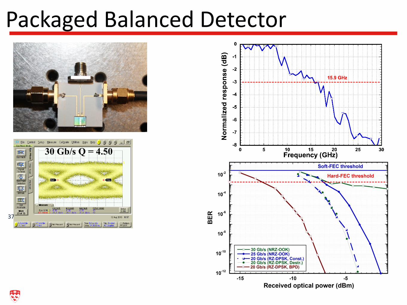
30 Gb/s Q = 4.50
Packaged Balanced Detector
37

© 2015 Odile Liboiron-‐Ladouceur
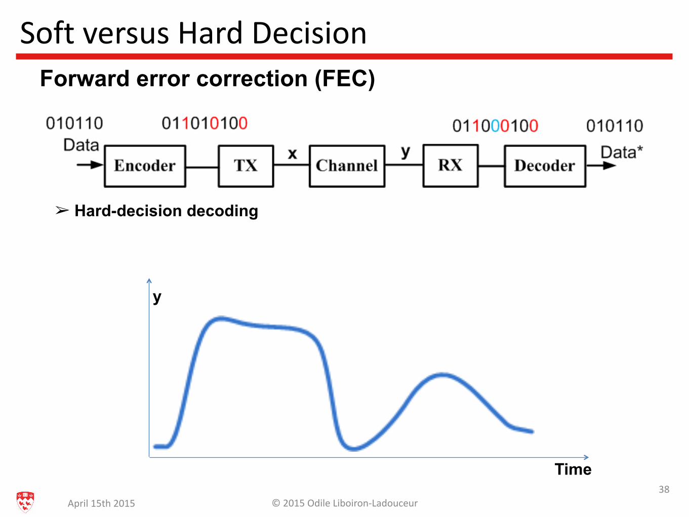
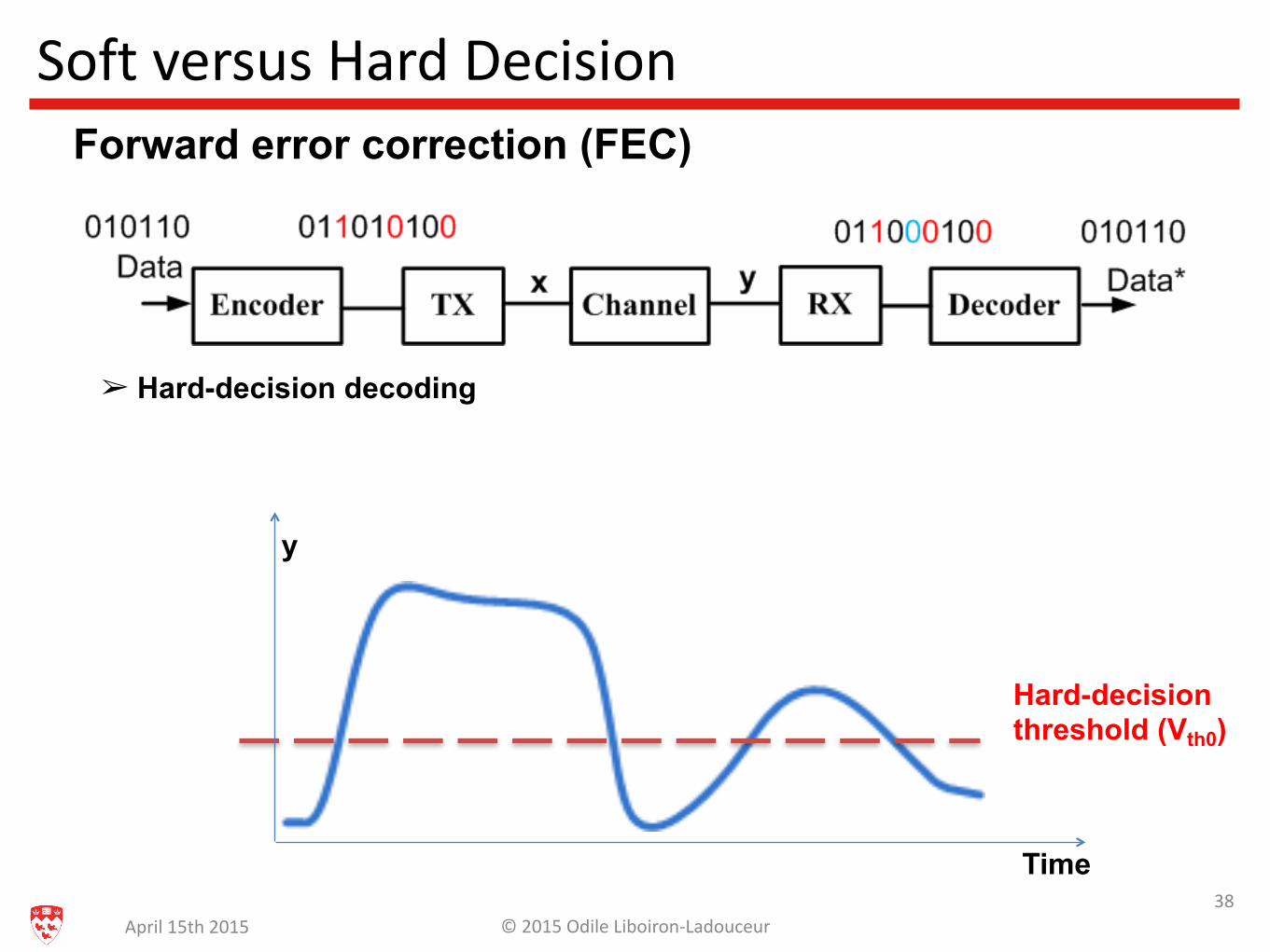
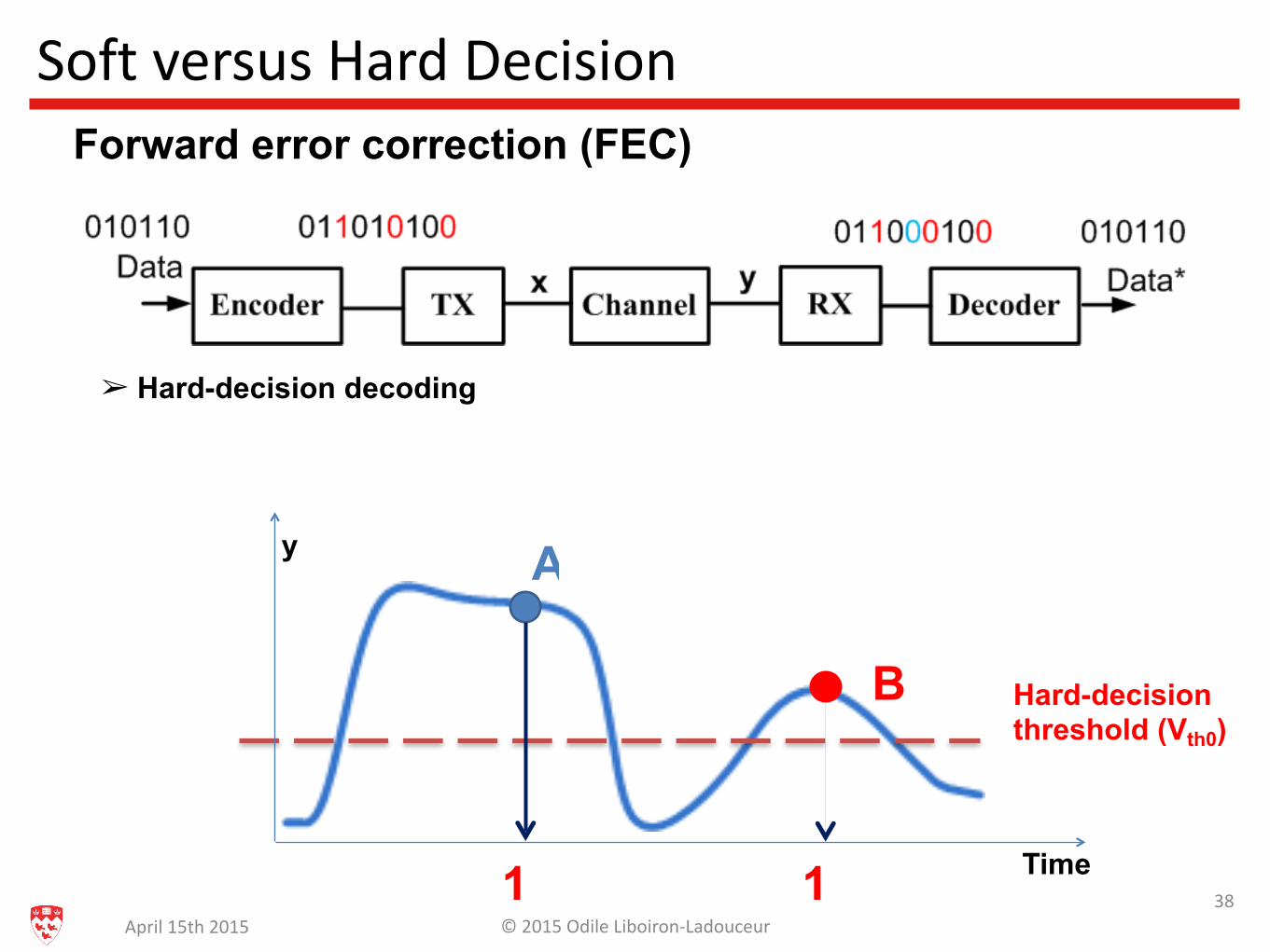
Soft versus Hard Decision
April 15th 2015
Forward error correction (FEC)
38

© 2015 Odile Liboiron-‐Ladouceur
Soft versus Hard Decision
April 15th 2015
Hard-decision decoding
Forward error correction (FEC)
38
© 2015 Odile Liboiron-‐Ladouceur
Soft versus Hard Decision
April 15th 2015
Hard-decision decoding
y
Time
Forward error correction (FEC)
38
© 2015 Odile Liboiron-‐Ladouceur
Soft versus Hard Decision
April 15th 2015
Hard-decision decoding
y
Time
Hard-decision threshold (Vth0)
Forward error correction (FEC)
38
© 2015 Odile Liboiron-‐Ladouceur
Soft versus Hard Decision
April 15th 2015
Hard-decision decoding
A
B
1 1
y
Time
Hard-decision threshold (Vth0)
Forward error correction (FEC)
38

© 2015 Odile Liboiron-‐Ladouceur
Soft versus Hard Decision
April 15th 2015
Hard-decision decoding
Soft-decision decoding
Soft-decision threshold (Vth-1)
A
B
1 11 0
y
Time
Hard-decision threshold (Vth0)
Soft-decision threshold (Vth1)
Forward error correction (FEC)
38
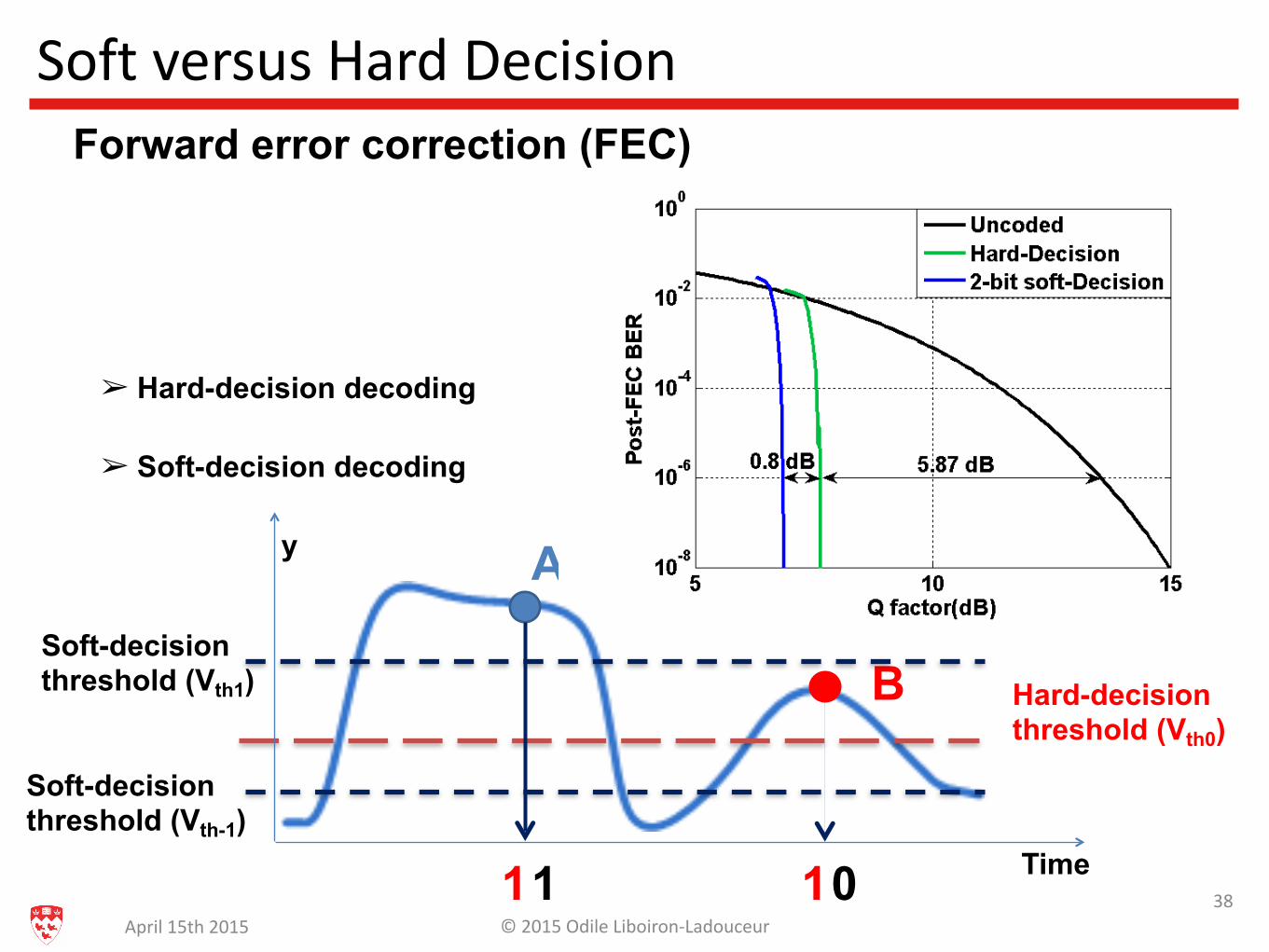
© 2015 Odile Liboiron-‐Ladouceur
Soft versus Hard Decision
April 15th 2015
Hard-decision decoding
Soft-decision decoding
Soft-decision threshold (Vth-1)
A
B
1 11 0
y
Time
Hard-decision threshold (Vth0)
Soft-decision threshold (Vth1)
Forward error correction (FEC)
38
© 2015 Odile Liboiron-‐Ladouceur
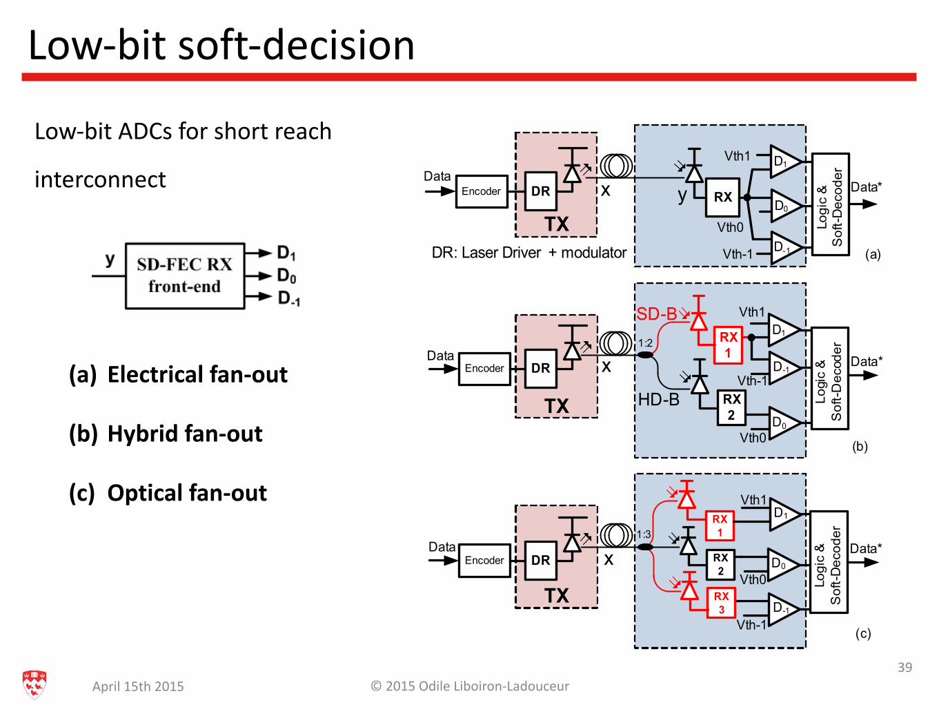
Low-‐bit soft-‐decision
April 15th 2015
(a) Electrical fan-‐out
(b) Hybrid fan-‐out
(c) Optical fan-‐out
TX
DREncoder RX
D1Vth1
D0
D-1Vth-1
Vth0 Logi
c &
S
oft-D
ecod
erData
RX1
D1
Vth1
D-1
D0
Vth-1
Vth0
RX2
(a)
(b)
RX1
Vth1
Vth0
RX2
(c)Vth-1
RX3
Data*
Logi
c &
S
oft-D
ecod
er
Data*
TX
DREncoderData
Logi
c &
S
oft-D
ecod
er
Data*
TX
DREncoderData
x
x
x
y
1:2
1:3
D1
D0
D-1
DR: Laser Driver + modulator
HD-B
SD-B
Low-‐bit ADCs for short reach
interconnect
39

© 2015 Odile Liboiron-‐Ladouceur
Low-‐bit Soft-‐Decision
April 15th 2015
Coding gain over uncoded: 7.06, and 8.25 for post-‐FEC BER of 10-‐7, and 10-‐9. Coding gain over hard-‐decision is 1.9 dB.
M. Sakib, M. Moayedi, W. Gross, and O. Liboiron-‐Ladouceur, "A 45 Gb/s Low Complexity Optical Front-‐End for Soft-‐Decision LDPC Decoders,” Optics Express, vol. 20, no. 16, pp. 18336–18347, July 2012.
40

© 2015 Odile Liboiron-‐Ladouceur
Soft-‐Decision in Coherent systems
41April 15th 2015
Sakib, M.N.; Hai, M.S.; Liboiron-‐Ladouceur, O., "A Silicon Photonic Integrated Packaged Coherent Receiver Front-‐End For Soft-‐Decision Decoding," Lightwave Technology, Journal of , vol.32, no.24, pp.4753,4758, Dec.15, 15 2014
• 6.2 dB for post-‐FEC BER of 10-‐7 for uncoded. • Coding gain is 1.8 dB when compared to hard-‐decision decoding.
• Degradation from 8-‐bit ADC, 1.7 dB. • Improvement over RS(255,239) of 2.2 dB.

© 2015 L. ChrostowskiSi-EPIC CREATE42
High-speed detection at two micrometreswith monolithic silicon photodiodesJason J. Ackert1*, David J. Thomson2, Li Shen2, Anna C. Peacock2, Paul E. Jessop3, Graham T. Reed2,Goran Z. Mashanovich2 and Andrew P. Knights1
With continued steep growth in the volume of data transmittedover optical networks there is a widely recognized need formore sophisticated photonics technologies to forestall a‘capacity crunch’1. A promising solution is to open new spectralregions at wavelengths near 2 μm and to exploit the long-wave-length transmission and amplification capabilities of hollow-core photonic-bandgap fibres2,3 and the recently availablethulium-doped fibre amplifiers4. To date, photodetectordevices for this window have largely relied on III–V materials5
or, where the benefits of integration with silicon photonicsare sought, GeSn alloys, which have been demonstrated thusfar with only limited utility6–9. Here, we describe a siliconphotodiode operating at 20 Gbit s–1 in this wavelength region.The detector is compatible with standard silicon processingand is integrated directly with silicon-on-insulator waveguides,which suggests future utility in silicon-based mid-infraredintegrated optics for applications in communications.
The advantages of silicon photonics, which have been well docu-mented for traditional communication wavelengths around 1.3 and1.5 µm (refs 8,9), extend to operation in the mid-infrared (MIR)region10. Silicon photonic components are fabricated using comp-lementary metal–oxide semiconductor (CMOS)-compatible tech-nologies, with the potential for integration with electronic control.Recently, groups have demonstrated several silicon-based com-ponents operating in the MIR wavelength range of 2–20 μm, includ-ing low-loss waveguides, couplers, splitters and multiplexers11, aswell as some with hybrid active functionality12,13. However, photo-detectors that are compatible with silicon waveguides, are capableof detection beyond 2 μm, and operate at the bandwidths requiredby future optical communication networks remain elusive. The sig-nificant success of the integration of germanium with silicon toproduce fast photodetection at wavelengths around 1.3 and 1.55 µmcannot be extended to 2 µm because of the cutoff wavelengthof germanium. Although GeSn alloys offer considerable potentialto extend the sensitivity of germanium technologies into theMIR, these material systems currently lag behind pure germaniumdetection schemes. At this early stage in development, theGeSn devices reported thus far have relatively high leakagecurrent with no high-speed functionality demonstrated near 2 µm(ref. 13). An interesting alternative approach, with potential for inte-gration with silicon, comprises the use of graphene-based photo-detectors14, but the waveguide-integrated devices demonstrated todate have not demonstrated efficient responsivity and highbandwidth simultaneously.
In this Letter we demonstrate photodetection in the avalanchemode at a wavelength of 1.96 µm with a bit rate of 20 Gbit s–1 inan experimental set-up that makes use of a thulium-doped fibre
amplifier (TDFA)4. This is the highest demonstrated bit rate foran integrated detector in the 1.81–2.04 µm gain window of thisoptical amplifier, and was accomplished with a silicon waveguideutilizing defect-mediated absorption, which extends the cutoffwavelength beyond the intrinsic value of 1.1 µm via deep levels.Such detectors have been explored at wavelengths around 1.55µm, with devices showing high responsivity at 10 Gbit s–1 whenoperated in the avalanche mode15,16. Due to the relatively weakinteraction of sub-bandgap light with lattice defects, the detectorsrequire absorption regions on the order of hundreds of micrometresin length. However, this does not necessarily inhibit high-speedoperation in optimally designed structures. Whereas furtherreduced sensitivity at wavelengths longer than 1.55 µm has beendemonstrated, high-bit-rate detection has not17–19. Specifically,such detectors have shown absorption at wavelengths of 2.2 µm,but with a responsivity of just 0.005 AW–1 and a small signal band-width of only 1.7 GHz (ref. 19). High-speed performance is essentialif the TDFA-compatible spectral region is to be utilized in next-gen-eration communication systems.
The most distinctive feature of the device fabrication process forthe current work is its simplicity, as no heterogeneous integration isnecessary. The detectors consist of silicon-on-insulator (SOI) wave-guides with a lateral p–i–n junction. Absorption is due to latticedefects introduced by low-dose inert ion implantation. The activedefect in this case is the silicon divacancy, which has been shownpreviously to mediate photodetection for wavelengths around1.5 µm, a process described in detail elsewhere20. An etchedwindow in the oxide cladding above the waveguide serves as amask to target the intrinsic region of the p–i–n diode with theinert implantation. The heavily doped p and n regions of thedevice are positioned 300 nm from the waveguide sidewall tomanage propagation loss. Aluminium contacts are positionedseveral micrometres away from the waveguide. Coupling lightfrom an external fibre to the detector is accomplished byinverted-taper waveguides that extend to the edge of the chip andprovide broadband access21. The widths of the couplers taper line-arly from 1 µm to 180 nm over a length of 200 nm, and terminatewithin a few micrometres of the sample edge. Further details ofthe fabrication can be found in the Methods. Scanning electronmicroscope (SEM) images (with false colour) are presented inFig. 1, as well as a cross-section obtained via focused ion beamSEM (Fig. 1b).
The steady-state response of the devices was investigated overthe wavelength range of 1.96–2.5 µm. Figure 2a presents thecurrent–voltage characteristics of a 1-mm-long photodiode at awavelength of 2.02 µm for a fibre launched power of 1 mW, withan external responsivity (photocurrent/waveguide coupled power)
1Department of Engineering Physics, McMaster University, 1280 Main St West, Hamilton, Ontario L8S 4L7, Canada. 2Optoelectronics Research Centre,University of Southampton, Highfield, Southampton, Hampshire SO17 1BJ, UK. 3Department of Physics and Computer Science, Wilfrid Laurier University,75 University Avenue West, Waterloo, Ontario N2L 3C5, Canada. *e-mail: [email protected]
LETTERSPUBLISHED ONLINE: 25 MAY 2015 | DOI: 10.1038/NPHOTON.2015.81
NATURE PHOTONICS | ADVANCE ONLINE PUBLICATION | www.nature.com/naturephotonics 1
of 0.3 ± 0.02 AW–1 at a bias of 30 V with a dark current less than1 µA. Although the responsivity is lower than reported for siliconavalanche diodes at 1.55 µm (refs 15,16), it remains acceptable fornetwork development. The decrease is attributed to two factors: areduced cross-section for photon/defect interaction22 and asmaller modal confinement factor. The latter leads to reducedabsorption in the implanted silicon, increased coupling to the sub-strate, and increased absorption in the heavily doped regions. Agreater confinement factor, and thus more sensitive detector,could be achieved by optimizing the waveguide height and width.For instance, optical mode simulations show that increasing theheight from 220 to 300 nm would result in an improvement of atleast 15% in the confinement factor of the waveguide region.
The photodiode current versus wavelength was measured using atunable Cr2+:ZnSe laser. The optical power exiting the launch fibrewas set to 10 mW, followed by an estimated coupling loss of 4 dB at2.02 µm. A plot of photodiode current versus wavelength is shownin Fig. 2b for reverse biases of 25 V and 10 V. We observed areduction in photocurrent of 14 dB from 1.96 to 2.5 µm. Thedecrease in wavelength response for this device is not wholly incon-sistent with the results obtained by Thomson and colleagues23, whoshowed a 9 dB reduction when changing the wavelength from 2 to2.5 µm. It is noted that in Thomson’s work, the waveguide cross-section was greater than 10 µm2, whereas in the current work thecross-section is 0.22 µm2. Figure 2c shows the photocurrent as afunction of externally launched optical power at a wavelength of2.2 µm. The response varies as a fractional exponent of the input
power and demonstrates that at these wavelengths two-photonabsorption is not the primary absorption mechanism. Rather, theintroduction of lattice defects (and corresponding mid-bandgaplevels) permits a photon–phonon mechanism for electron–holepair generation, as was described by Logan and co-authors20. Thissublinear response is probably caused by the saturation ofdefect centres.
To determine the photodiode’s potential for MIR communi-cations applications, high-speed characterization was carried outat a wavelength of 1.96 µm. The optical set-up consisted of a
a
b
c
1.00
0.10
Illuminated
25 V
5 V
10 V
15 V
Responsivity (A W
−1)
0.01
10−3
10−4
10−3
10−4
Dark
Dark current
10−5
10−6
Dio
de c
urre
nt (A
)
Reverse bias voltage (V)0
1.9 2.0 2.1 2.2 2.3Wavelength (µm)
1 10External launched power (mW)
2.4 2.5
5 10 15 20 25 30
10−7
10−3
10−4
10−5
10−6
Dio
de c
urre
nt (A
)
10−4
10−5
y ≈ x0.6
y ≈ x0.7
10−6
Dio
de c
urre
nt (A
)
10−7
10−8
λ = 2.02 µmLength = 1 mm
λ = 2.20 µm
25 V10 V
Figure 2 | Steady-state photodiode current measurements. a, Photocurrent/responsivity versus reverse bias voltage for a 1-mm-long photodiode at awavelength of 2.02 µm (external launch power of 1 mW). b, Photocurrentversus wavelength for a 1-mm-long device (external launch power of10 mW). c, Photocurrent as a function of input power for a wavelength of2.2 µm, measured exiting the launch fibre. A sublinear response is observed.
a
b 1,000
300 90 pn
Metal
Oxide
Silicon
Slab region and taper
Waveguide and oxide windowMetal
10 µm
5 µm
220
Figure 1 | SEM images of the photodetector. a, Plan-view SEM image of thedetector. b, Cross-sectional view of the same device obtained via a focusedion beam SEM. Inset in b: schematic cross-section of the silicon waveguide,with dimensions labelled in nanometres, and with the transverse electricmode at 2 µm overlaid. Images are shown in false colour to distinguishthe materials.
LETTERS NATURE PHOTONICS DOI: 10.1038/NPHOTON.2015.81
NATURE PHOTONICS | ADVANCE ONLINE PUBLICATION | www.nature.com/naturephotonics2

© 2015 L. ChrostowskiSi-EPIC CREATE43
1.96 µm laser diode, a TDFA4 and a 10 GHz LiNbO3 modulatorbiased at quadrature and operating with a non-return-to-zeroon–off keying, pseudo-random binary signal of length 27 – 1 (seeMethods for further details of the set-up). Figure 3a presents aneye diagram from a 1 mm diode operating at 20 Gbit s–1, represent-ing the fastest operation of an integrated photodetector of anydesign at this wavelength. Due to the lack of a fast reference photo-diode at 2 µm we were unable to record the LiNbO3 modulatorresponse at this bit rate. However, in an attempt to provide quanti-tative information on the bandwidth limit of operation, thesmall signal response of the detector was characterized for a wave-length of 1.55 µm (thus utilizing the standard high-speed character-ization equipment available at this wavelength), with theresults shown in Fig. 4. The 1-mm-long detector shows a 3 dB band-width of 12.5 GHz, while the 200-µm-long device shows 15 GHz.The measured capacitance of our 1-mm-long detector is 260 ± 10 fF.With a 50 Ω load this provides an RC limited bandwidthof ∼12 GHz, which is consistent with the small signal resultsat 1,550 nm.
Operation at different reverse-bias voltages (Fig. 3) allows us todismiss a gain-limited bandwidth. For a detector working in theavalanche regime, the carrier multiplication time imposes a limiton the operation speed24. Figure 3a–c shows 20 Gbit s–1 eye dia-grams for a 1-mm-long detector operating at three differentreverse-bias voltages (27, 20 and 15 V). At these bias levels thedetector is in the avalanche regime, yet the higher bias increasesthe signal magnitude without noticeable degradation of the riseand fall times.
The detector was also operated beyond 20 Gbit s–1. Figure 3d, forexample, shows a 28 Gbit s–1 eye diagram. The fact that the eye isstill open is a promising result, although the relative closure com-pared to the 20 Gbit s–1 data indicates that the detector is operating
ba
dc
15 V 20 Gbit s−1
27 V 20 Gbit s−1 20 V 20 Gbit s−1
λ = 1.96 µm 28 Gbit s−1
Number averages = 9 Number averages = 4
Number averages = 6Number averages = 14
Start Start
Start
Figure 3 | Eye diagrams for a 1-mm-long detector operating at a wavelength of 1.96 μm. The timescale is 20 ps div−1 and the pseudo-random binarysequence length is 27 – 1 for all images. a, 20 Gbit s−1 at 27 V reverse bias. The vertical scale is 6.7 mV div−1. b, 20 Gbit s−1 at 20 V reverse bias. The verticalscale is 2.0 mV div−1. c, 20 Gbit s−1 at 15 V reverse bias. The vertical scale is 2.0 mV div−1. d, 28 Gbit s−1 at 27 V reverse bias. The vertical scale is 6.7 mV div−1.
0
L = 200 µm15 GHz
L = 1 mm12.5 GHz
0 5 10 15Frequency (GHz)
10 25 30
Nor
mal
ized
resp
onse
(dB)
−3
−6
−9
−12
−15
−18
Figure 4 | The small signal frequency response at a wavelength of1,550 nm. Responses for 1-mm-long (red) and 200-µm-long (blue)photodiodes are shown, with a reverse bias of 30 V. The 1 mm deviceshows a 3 dB bandwidth of 12.5 GHz whereas the 200 µm device showsa bandwidth of 15 GHz.
NATURE PHOTONICS DOI: 10.1038/NPHOTON.2015.81 LETTERS
NATURE PHOTONICS | ADVANCE ONLINE PUBLICATION | www.nature.com/naturephotonics 3
20 Gb/s Eye diagram
1.96 µm laser diode, a TDFA4 and a 10 GHz LiNbO3 modulatorbiased at quadrature and operating with a non-return-to-zeroon–off keying, pseudo-random binary signal of length 27 – 1 (seeMethods for further details of the set-up). Figure 3a presents aneye diagram from a 1 mm diode operating at 20 Gbit s–1, represent-ing the fastest operation of an integrated photodetector of anydesign at this wavelength. Due to the lack of a fast reference photo-diode at 2 µm we were unable to record the LiNbO3 modulatorresponse at this bit rate. However, in an attempt to provide quanti-tative information on the bandwidth limit of operation, thesmall signal response of the detector was characterized for a wave-length of 1.55 µm (thus utilizing the standard high-speed character-ization equipment available at this wavelength), with theresults shown in Fig. 4. The 1-mm-long detector shows a 3 dB band-width of 12.5 GHz, while the 200-µm-long device shows 15 GHz.The measured capacitance of our 1-mm-long detector is 260 ± 10 fF.With a 50 Ω load this provides an RC limited bandwidthof ∼12 GHz, which is consistent with the small signal resultsat 1,550 nm.
Operation at different reverse-bias voltages (Fig. 3) allows us todismiss a gain-limited bandwidth. For a detector working in theavalanche regime, the carrier multiplication time imposes a limiton the operation speed24. Figure 3a–c shows 20 Gbit s–1 eye dia-grams for a 1-mm-long detector operating at three differentreverse-bias voltages (27, 20 and 15 V). At these bias levels thedetector is in the avalanche regime, yet the higher bias increasesthe signal magnitude without noticeable degradation of the riseand fall times.
The detector was also operated beyond 20 Gbit s–1. Figure 3d, forexample, shows a 28 Gbit s–1 eye diagram. The fact that the eye isstill open is a promising result, although the relative closure com-pared to the 20 Gbit s–1 data indicates that the detector is operating
ba
dc
15 V 20 Gbit s−1
27 V 20 Gbit s−1 20 V 20 Gbit s−1
λ = 1.96 µm 28 Gbit s−1
Number averages = 9 Number averages = 4
Number averages = 6Number averages = 14
Start Start
Start
Figure 3 | Eye diagrams for a 1-mm-long detector operating at a wavelength of 1.96 μm. The timescale is 20 ps div−1 and the pseudo-random binarysequence length is 27 – 1 for all images. a, 20 Gbit s−1 at 27 V reverse bias. The vertical scale is 6.7 mV div−1. b, 20 Gbit s−1 at 20 V reverse bias. The verticalscale is 2.0 mV div−1. c, 20 Gbit s−1 at 15 V reverse bias. The vertical scale is 2.0 mV div−1. d, 28 Gbit s−1 at 27 V reverse bias. The vertical scale is 6.7 mV div−1.
0
L = 200 µm15 GHz
L = 1 mm12.5 GHz
0 5 10 15Frequency (GHz)
10 25 30
Nor
mal
ized
resp
onse
(dB)
−3
−6
−9
−12
−15
−18
Figure 4 | The small signal frequency response at a wavelength of1,550 nm. Responses for 1-mm-long (red) and 200-µm-long (blue)photodiodes are shown, with a reverse bias of 30 V. The 1 mm deviceshows a 3 dB bandwidth of 12.5 GHz whereas the 200 µm device showsa bandwidth of 15 GHz.
NATURE PHOTONICS DOI: 10.1038/NPHOTON.2015.81 LETTERS
NATURE PHOTONICS | ADVANCE ONLINE PUBLICATION | www.nature.com/naturephotonics 3
15 GHz EO bandwidth
Responsivity up to 0.3 A/W
of 0.3 ± 0.02 AW–1 at a bias of 30 V with a dark current less than1 µA. Although the responsivity is lower than reported for siliconavalanche diodes at 1.55 µm (refs 15,16), it remains acceptable fornetwork development. The decrease is attributed to two factors: areduced cross-section for photon/defect interaction22 and asmaller modal confinement factor. The latter leads to reducedabsorption in the implanted silicon, increased coupling to the sub-strate, and increased absorption in the heavily doped regions. Agreater confinement factor, and thus more sensitive detector,could be achieved by optimizing the waveguide height and width.For instance, optical mode simulations show that increasing theheight from 220 to 300 nm would result in an improvement of atleast 15% in the confinement factor of the waveguide region.
The photodiode current versus wavelength was measured using atunable Cr2+:ZnSe laser. The optical power exiting the launch fibrewas set to 10 mW, followed by an estimated coupling loss of 4 dB at2.02 µm. A plot of photodiode current versus wavelength is shownin Fig. 2b for reverse biases of 25 V and 10 V. We observed areduction in photocurrent of 14 dB from 1.96 to 2.5 µm. Thedecrease in wavelength response for this device is not wholly incon-sistent with the results obtained by Thomson and colleagues23, whoshowed a 9 dB reduction when changing the wavelength from 2 to2.5 µm. It is noted that in Thomson’s work, the waveguide cross-section was greater than 10 µm2, whereas in the current work thecross-section is 0.22 µm2. Figure 2c shows the photocurrent as afunction of externally launched optical power at a wavelength of2.2 µm. The response varies as a fractional exponent of the input
power and demonstrates that at these wavelengths two-photonabsorption is not the primary absorption mechanism. Rather, theintroduction of lattice defects (and corresponding mid-bandgaplevels) permits a photon–phonon mechanism for electron–holepair generation, as was described by Logan and co-authors20. Thissublinear response is probably caused by the saturation ofdefect centres.
To determine the photodiode’s potential for MIR communi-cations applications, high-speed characterization was carried outat a wavelength of 1.96 µm. The optical set-up consisted of a
a
b
c
1.00
0.10
Illuminated
25 V
5 V
10 V
15 V
Responsivity (A W
−1)
0.01
10−3
10−4
10−3
10−4
Dark
Dark current
10−5
10−6
Dio
de c
urre
nt (A
)
Reverse bias voltage (V)0
1.9 2.0 2.1 2.2 2.3Wavelength (µm)
1 10External launched power (mW)
2.4 2.5
5 10 15 20 25 30
10−7
10−3
10−4
10−5
10−6
Dio
de c
urre
nt (A
)
10−4
10−5
y ≈ x0.6
y ≈ x0.7
10−6
Dio
de c
urre
nt (A
)
10−7
10−8
λ = 2.02 µmLength = 1 mm
λ = 2.20 µm
25 V10 V
Figure 2 | Steady-state photodiode current measurements. a, Photocurrent/responsivity versus reverse bias voltage for a 1-mm-long photodiode at awavelength of 2.02 µm (external launch power of 1 mW). b, Photocurrentversus wavelength for a 1-mm-long device (external launch power of10 mW). c, Photocurrent as a function of input power for a wavelength of2.2 µm, measured exiting the launch fibre. A sublinear response is observed.
a
b 1,000
300 90 pn
Metal
Oxide
Silicon
Slab region and taper
Waveguide and oxide windowMetal
10 µm
5 µm
220
Figure 1 | SEM images of the photodetector. a, Plan-view SEM image of thedetector. b, Cross-sectional view of the same device obtained via a focusedion beam SEM. Inset in b: schematic cross-section of the silicon waveguide,with dimensions labelled in nanometres, and with the transverse electricmode at 2 µm overlaid. Images are shown in false colour to distinguishthe materials.
LETTERS NATURE PHOTONICS DOI: 10.1038/NPHOTON.2015.81
NATURE PHOTONICS | ADVANCE ONLINE PUBLICATION | www.nature.com/naturephotonics2
High-speed detection at two micrometreswith monolithic silicon photodiodesJason J. Ackert1*, David J. Thomson2, Li Shen2, Anna C. Peacock2, Paul E. Jessop3, Graham T. Reed2,Goran Z. Mashanovich2 and Andrew P. Knights1
With continued steep growth in the volume of data transmittedover optical networks there is a widely recognized need formore sophisticated photonics technologies to forestall a‘capacity crunch’1. A promising solution is to open new spectralregions at wavelengths near 2 μm and to exploit the long-wave-length transmission and amplification capabilities of hollow-core photonic-bandgap fibres2,3 and the recently availablethulium-doped fibre amplifiers4. To date, photodetectordevices for this window have largely relied on III–V materials5
or, where the benefits of integration with silicon photonicsare sought, GeSn alloys, which have been demonstrated thusfar with only limited utility6–9. Here, we describe a siliconphotodiode operating at 20 Gbit s–1 in this wavelength region.The detector is compatible with standard silicon processingand is integrated directly with silicon-on-insulator waveguides,which suggests future utility in silicon-based mid-infraredintegrated optics for applications in communications.
The advantages of silicon photonics, which have been well docu-mented for traditional communication wavelengths around 1.3 and1.5 µm (refs 8,9), extend to operation in the mid-infrared (MIR)region10. Silicon photonic components are fabricated using comp-lementary metal–oxide semiconductor (CMOS)-compatible tech-nologies, with the potential for integration with electronic control.Recently, groups have demonstrated several silicon-based com-ponents operating in the MIR wavelength range of 2–20 μm, includ-ing low-loss waveguides, couplers, splitters and multiplexers11, aswell as some with hybrid active functionality12,13. However, photo-detectors that are compatible with silicon waveguides, are capableof detection beyond 2 μm, and operate at the bandwidths requiredby future optical communication networks remain elusive. The sig-nificant success of the integration of germanium with silicon toproduce fast photodetection at wavelengths around 1.3 and 1.55 µmcannot be extended to 2 µm because of the cutoff wavelengthof germanium. Although GeSn alloys offer considerable potentialto extend the sensitivity of germanium technologies into theMIR, these material systems currently lag behind pure germaniumdetection schemes. At this early stage in development, theGeSn devices reported thus far have relatively high leakagecurrent with no high-speed functionality demonstrated near 2 µm(ref. 13). An interesting alternative approach, with potential for inte-gration with silicon, comprises the use of graphene-based photo-detectors14, but the waveguide-integrated devices demonstrated todate have not demonstrated efficient responsivity and highbandwidth simultaneously.
In this Letter we demonstrate photodetection in the avalanchemode at a wavelength of 1.96 µm with a bit rate of 20 Gbit s–1 inan experimental set-up that makes use of a thulium-doped fibre
amplifier (TDFA)4. This is the highest demonstrated bit rate foran integrated detector in the 1.81–2.04 µm gain window of thisoptical amplifier, and was accomplished with a silicon waveguideutilizing defect-mediated absorption, which extends the cutoffwavelength beyond the intrinsic value of 1.1 µm via deep levels.Such detectors have been explored at wavelengths around 1.55µm, with devices showing high responsivity at 10 Gbit s–1 whenoperated in the avalanche mode15,16. Due to the relatively weakinteraction of sub-bandgap light with lattice defects, the detectorsrequire absorption regions on the order of hundreds of micrometresin length. However, this does not necessarily inhibit high-speedoperation in optimally designed structures. Whereas furtherreduced sensitivity at wavelengths longer than 1.55 µm has beendemonstrated, high-bit-rate detection has not17–19. Specifically,such detectors have shown absorption at wavelengths of 2.2 µm,but with a responsivity of just 0.005 AW–1 and a small signal band-width of only 1.7 GHz (ref. 19). High-speed performance is essentialif the TDFA-compatible spectral region is to be utilized in next-gen-eration communication systems.
The most distinctive feature of the device fabrication process forthe current work is its simplicity, as no heterogeneous integration isnecessary. The detectors consist of silicon-on-insulator (SOI) wave-guides with a lateral p–i–n junction. Absorption is due to latticedefects introduced by low-dose inert ion implantation. The activedefect in this case is the silicon divacancy, which has been shownpreviously to mediate photodetection for wavelengths around1.5 µm, a process described in detail elsewhere20. An etchedwindow in the oxide cladding above the waveguide serves as amask to target the intrinsic region of the p–i–n diode with theinert implantation. The heavily doped p and n regions of thedevice are positioned 300 nm from the waveguide sidewall tomanage propagation loss. Aluminium contacts are positionedseveral micrometres away from the waveguide. Coupling lightfrom an external fibre to the detector is accomplished byinverted-taper waveguides that extend to the edge of the chip andprovide broadband access21. The widths of the couplers taper line-arly from 1 µm to 180 nm over a length of 200 nm, and terminatewithin a few micrometres of the sample edge. Further details ofthe fabrication can be found in the Methods. Scanning electronmicroscope (SEM) images (with false colour) are presented inFig. 1, as well as a cross-section obtained via focused ion beamSEM (Fig. 1b).
The steady-state response of the devices was investigated overthe wavelength range of 1.96–2.5 µm. Figure 2a presents thecurrent–voltage characteristics of a 1-mm-long photodiode at awavelength of 2.02 µm for a fibre launched power of 1 mW, withan external responsivity (photocurrent/waveguide coupled power)
1Department of Engineering Physics, McMaster University, 1280 Main St West, Hamilton, Ontario L8S 4L7, Canada. 2Optoelectronics Research Centre,University of Southampton, Highfield, Southampton, Hampshire SO17 1BJ, UK. 3Department of Physics and Computer Science, Wilfrid Laurier University,75 University Avenue West, Waterloo, Ontario N2L 3C5, Canada. *e-mail: [email protected]
LETTERSPUBLISHED ONLINE: 25 MAY 2015 | DOI: 10.1038/NPHOTON.2015.81
NATURE PHOTONICS | ADVANCE ONLINE PUBLICATION | www.nature.com/naturephotonics 1

SiEPIC Actives 2014
Applications of Photonic Crystals in Hybrid Silicon Integrated Photonic Circuits: Single Photon Superconducting Detectors
Jeff F. Young,
Department of Physics and Astronomy,
Advanced Materials and Process Engineering Laboratory University of British Columbia
44

SiEPIC Actives 2014
Superconducting Nanowire Single Photon Detectors
45
IBiasIBias
V = 0
NbN, NbTiN, Nb Few nm Thick About 100nm Wide
Working Principle:
Typical Meandering Implementation:
critically-‐biased superconducting nanowire

SiEPIC Actives 2014
Superconducting Nanowire Single Photon Detectors
45
IBiasIBias
V = 0
NbN, NbTiN, Nb Few nm Thick About 100nm Wide
V ≠ 0
IBias
hνWorking Principle:
Typical Meandering Implementation:
critically-‐biased superconducting nanowire

SiEPIC Actives 2014
Design Concept
46
M.K. Akhlaghi, E. Schelew and J.F. Young, arXiv:submit/1060133 \/, (5 Sep 2014).
SiEPIC Actives 2014
Results
47
• 200 nm SOI, with 8 nm of NiTiN superconducting film [Tc=7.2K, Jc(T=0)=7.6 x 10⁶ A/cm2]
• 8.5 µm long, 35 nm wide NiTiN nanowire “perfect absorber” • 96% Q.E.; Dark rate < 0.1 Hz; < 7 ns reset time.
Single PhotonDetection
M.K. Akhlaghi, E. Schelew and J.F. Young, arXiv:submit/1060133 \/, (5 Sep 2014).

SiEPIC Workshop – Active Silicon PhotonicsSi-EPIC CREATE
PN Depletion Modulator – Michelson interferometric modulator
• Reverse-biased PN junction
• Interferometric configuration
48
“High-speed compact silicon photonic Michelson interferometric modulator”, David Patel, Venkat Veerasubramanian, Samir Ghosh, Alireza Samani, Qiuhang Zhong, and David V. Plant. Optics Express, Vol. 22, Issue 22, pp. 26788-26802 (2014) http://dx.doi.org/10.1364/OE.22.026788
phase shifters, we operate the modulator near, but not exactly at, 1550 nm.The phase shifter length was chosen to be smaller than 1/10th of the effective microwave
wavelength le f f for lumped element modeling and analysis. Figure 1(b) shows the criticallength for this rule of thumb, Lcritical = le f f /10, as a function of frequency. The microwaveeffective wavelength for a quasi-TEM mode with coplanar strip electrodes loaded with a p-njunction was obtained from simulations in ANSYS HFSS. This simulation considered the fre-quency dependence of the effective index, which at 20 GHz was found to be 3.0 using estimatedresistance and capacitance of the p-n junction at 0 V and 2.1 for the case of the unloaded elec-trode. The phase shifter was designed to be 500-µm long in order to be considered electricallysmall up to at least 20 GHz. In addition, it is assumed that the optical transit time is muchshorter than the microwave travel time.
MIM designs were fabricated using a commercially available process at the Institute of Mi-croelectronics (IME) A*STAR (Singapore) on a SOI wafer with a 2 µm buried oxide (BOX)layer and a 220-nm thick top-silicon. This process had a single 2-µm thick aluminum intercon-nect metal layer, aluminum vias, and non-silicide contacts. The designs used 130 nm etch stepsfor creating rib waveguides and adiabatic directional couplers, 220 nm deep etch for channelwaveguides, and 70 nm etch steps for focused grating couplers.
Modulating diodes were developed in both p-n and p-i-n junction configurations. Figure 2(a)shows the p-n junction geometry and Fig. 2(b) shows the p-i-n junction cross-section. Higherconcentration dopants (p++ and n++) are used for ohmic contacts and the lower concentrationdopants (p and n) are used in the region of the waveguide where the optical field is most concen-trated. Similar to [7, 9], an offset of 100 nm relative to the center of the waveguide was used inthe p-n junctions to increase the mode overlap with the p-type semiconductor. This offset wasexpected to improve the modulation efficiency because the plasma dispersion effect is moresensitive to changes in free hole concentration [4].
n++n
p++p2 μm
220 nm 90 nm
500 nm
1 μm
1.73 μm
350 nm
SiO2
Si SubstrateBOX
2 μm
Al
(a) (b)
(c) (d)
Fig. 2. Cross-section of the fabricated (a) p-n, and (b) p-i-n MIM. Simulated depletionregion (delineated by white lines), and doping density (positive for n-type) of the (c) p-nand (d) p-i-n junctions at 0 V.
The dopant concentration and distribution, specific to this process, was simulated using thefoundry implant and annealing conditions with the Synopsys Sentaurus Process software. Theprocess simulation used Synopsys’s advanced calibration parameters. The simulations showedpeak p++, p, n, and n++ dopant active concentrations of 3.91019, 7.81017, 2.11018, and9.71019 cm3, respectively. The dopant distribution and concentration for the p-n and p-i-njunction is displayed in Figs. 2(c) and 2(d), respectively. A device simulation was subsequentlyperformed using Synopsys Sentaurus Device to obtain the distribution of free carriers in the
#221586 - $15.00 USD Received 25 Aug 2014; revised 9 Oct 2014; accepted 9 Oct 2014; published 21 Oct 2014(C) 2014 OSA 3 November 2014 | Vol. 22, No. 22 | DOI:10.1364/OE.22.026788 | OPTICS EXPRESS 26791
for greater bandwidth. We also observed a good agreement between the measured result for thisdevice and data obtained from simulations using the tools and methods described in section 2.It is important to note that because of the non-linear nature of the phase shift as a functionof voltage, the Vp Lp figure-of-merit does not allow the accurate calculation of Vp for a givenmodulator length or Lp for a given voltage.
0 2 4 6 8
0
0.5
1
Reverse Bias Voltage [V]
Phas
eSh
ift[r
ad]
measuredsimulated
(a)
2 4 6 80.6
0.8
1
Reverse Bias Voltage [V]
V pL p
[V-c
m]
measuredsimulated
(b)
Fig. 4. Derived from measurement and simulated (a) phase shift, and (b) Vp Lp of the p-nMIM with reverse bias voltage.
The p-i-n junction based modulator under reverse bias shows negligible change in phasebecause of the large depletion region already overlapping the optical mode at equilibrium con-ditions. The optical mode sees minute differences from any additional carrier extraction withapplied voltage. In forward bias, insignificant phase shifts are observed below threshold. A pphase shift is observed with relatively small voltages after threshold because of the large num-ber of injected carriers. The large carrier injection also results in a greater loss, and for thissingle drive configuration produces an imbalance in losses between the two arms of the MIM.This leads to a reduced extinction ratio in the interferometer as represented by the transmissionspectra. From Figs. 3(e) and 3(f), it is observed that the p-i-n junction device reaches p phaseshift at a smaller forward bias voltage compared to the p-n junction based modulator. The p-n junction modulator has a p phase shift at 1.5 V forward bias, corresponding to a Vp Lp of0.075 V-cm, whereas the p-i-n junction modulator has a p phase shift at 1.15 V correspondingto a Vp Lp of 0.058 V-cm. Besides optical modulation, forward biased MIM can be of interestin switching applications, for instance, it can substitute the thermo-optic based MI switchesdemonstrated in [18].
3.2. Small signal characterization
The RF S11 parameters were measured using an Agilent 50 GHz lightwave component analyzer(LCA). The RF power on the LCA was set to -5.0 dBm corresponding to 0.356 Vpp in a 50 Wload, which is small enough to approximate the non-linear electro-optic (EO) response to alinear one. In addition, the wavelength was set to bias the modulator at quadrature point toensure linearity, and reduce spurious peaks and dips during measurement. The measured RFS11 and EO S21 for different reverse bias voltages is shown in Fig. 5. A 3-dB EO bandwidth of13.3 GHz is measured at 4 V bias. Marginal improvement in the 3-dB EO bandwidth is observedfor reverse bias greater than 4 V because of smaller reductions in depletion capacitance forhigher biases.
The S11 curves show high reflection, particularly at lower frequencies, which occurs becausethe p-n junction under reverse bias is essentially a capacitor that behaves as an open circuitat low frequencies. Since it is the voltage across the capacitance which performs the optical
#221586 - $15.00 USD Received 25 Aug 2014; revised 9 Oct 2014; accepted 9 Oct 2014; published 21 Oct 2014(C) 2014 OSA 3 November 2014 | Vol. 22, No. 22 | DOI:10.1364/OE.22.026788 | OPTICS EXPRESS 26794
0 2 4 6 8
0
2
4
6
Reverse Bias Voltage [V]
Mea
sure
dC
urre
nt[n
A]
p-n junctionp-i-n junction
(a)
0 0.5 1 1.5 2
0
20
40
60
Forward Bias Voltage [V]
Mea
sure
dC
urre
nt[m
A]
p-n junctionp-i-n Junction
(b)
1550 1550.5 1551 1551.5 1552
-20
-30
-40
ER
FSR
IL
Dl2V
Wavelength [nm]
Mea
sure
dPo
wer
[dB
m]
0 V2 V4 V6 V8 V
(c) Reverse bias p-n junction
1548 1548.5 1549 1549.5 1550 1550.5
40
20
Wavelength [nm]
Mea
sure
dPo
wer
[dB
m]
0 V2 V4 V6 V8 V
(d) Reverse bias p-i-n junction
1548 1548.5 1549 1549.5 1550 1550.5
50
40
30
20
10
Wavelength [nm]
Mea
sure
dPo
wer
[dB
m]
0.0 V0.5 V1.0 V1.5 V
(e) Forward bias p-n junction
1550 1550.5 1551 1551.5 1552 1552.5
50
40
30
20
10
Wavelength [nm]
Mea
sure
dPo
wer
[dB
m]
0.0 V0.8 V1.0 V1.1 V1.2 V
(f) Forward bias p-i-n junction
Fig. 3. I-V measurement of p-n and p-i-n junctions with (a) reverse bias, and (b) forwardbias. Measured transmission spectrum under reverse bias of (c) p-n and (d) p-i-n MIM.Measured transmission spectrum under forward bias of (e) p-n and (f) p-i-n MIM.
#221586 - $15.00 USD Received 25 Aug 2014; revised 9 Oct 2014; accepted 9 Oct 2014; published 21 Oct 2014(C) 2014 OSA 3 November 2014 | Vol. 22, No. 22 | DOI:10.1364/OE.22.026788 | OPTICS EXPRESS 26793
phase shifters, we operate the modulator near, but not exactly at, 1550 nm.The phase shifter length was chosen to be smaller than 1/10th of the effective microwave
wavelength le f f for lumped element modeling and analysis. Figure 1(b) shows the criticallength for this rule of thumb, Lcritical = le f f /10, as a function of frequency. The microwaveeffective wavelength for a quasi-TEM mode with coplanar strip electrodes loaded with a p-njunction was obtained from simulations in ANSYS HFSS. This simulation considered the fre-quency dependence of the effective index, which at 20 GHz was found to be 3.0 using estimatedresistance and capacitance of the p-n junction at 0 V and 2.1 for the case of the unloaded elec-trode. The phase shifter was designed to be 500-µm long in order to be considered electricallysmall up to at least 20 GHz. In addition, it is assumed that the optical transit time is muchshorter than the microwave travel time.
MIM designs were fabricated using a commercially available process at the Institute of Mi-croelectronics (IME) A*STAR (Singapore) on a SOI wafer with a 2 µm buried oxide (BOX)layer and a 220-nm thick top-silicon. This process had a single 2-µm thick aluminum intercon-nect metal layer, aluminum vias, and non-silicide contacts. The designs used 130 nm etch stepsfor creating rib waveguides and adiabatic directional couplers, 220 nm deep etch for channelwaveguides, and 70 nm etch steps for focused grating couplers.
Modulating diodes were developed in both p-n and p-i-n junction configurations. Figure 2(a)shows the p-n junction geometry and Fig. 2(b) shows the p-i-n junction cross-section. Higherconcentration dopants (p++ and n++) are used for ohmic contacts and the lower concentrationdopants (p and n) are used in the region of the waveguide where the optical field is most concen-trated. Similar to [7, 9], an offset of 100 nm relative to the center of the waveguide was used inthe p-n junctions to increase the mode overlap with the p-type semiconductor. This offset wasexpected to improve the modulation efficiency because the plasma dispersion effect is moresensitive to changes in free hole concentration [4].
(a) (b)
(c) (d)
Fig. 2. Cross-section of the fabricated (a) p-n, and (b) p-i-n MIM. Simulated depletionregion (delineated by white lines), and doping density (positive for n-type) of the (c) p-nand (d) p-i-n junctions at 0 V.
The dopant concentration and distribution, specific to this process, was simulated using thefoundry implant and annealing conditions with the Synopsys Sentaurus Process software. Theprocess simulation used Synopsys’s advanced calibration parameters. The simulations showedpeak p++, p, n, and n++ dopant active concentrations of 3.91019, 7.81017, 2.11018, and9.71019 cm3, respectively. The dopant distribution and concentration for the p-n and p-i-njunction is displayed in Figs. 2(c) and 2(d), respectively. A device simulation was subsequentlyperformed using Synopsys Sentaurus Device to obtain the distribution of free carriers in the
#221586 - $15.00 USD Received 25 Aug 2014; revised 9 Oct 2014; accepted 9 Oct 2014; published 21 Oct 2014(C) 2014 OSA 3 November 2014 | Vol. 22, No. 22 | DOI:10.1364/OE.22.026788 | OPTICS EXPRESS 26791
© 2015 L. ChrostowskiSi-EPIC CREATE
PN Depletion Modulator – Michelson interferometric modulator
49
“High-speed compact silicon photonic Michelson interferometric modulator”, David Patel, Venkat Veerasubramanian, Samir Ghosh, Alireza Samani, Qiuhang Zhong, and David V. Plant. Optics Express, Vol. 22, Issue 22, pp. 26788-26802 (2014) http://dx.doi.org/10.1364/OE.22.026788
limited only by the bandwidth of the coupling devices. Because their modulation is relativelyweak, long phase shifters are required which leads to a voltage-length trade-off for such mod-ulators. A longer modulator will require a traveling wave electrode design and operate at lowerdrive voltages for a given optical modulation amplitude (OMA). Shorter modulators requirelarger voltages for a similar OMA but can be effectively studied using lumped element circuitanalysis.
In Michelson interferometric modulators (MIMs) light travels through the phase shiftingregion twice compared to MZMs because of loop mirrors placed at one end of the modula-tor. When compared to nearly identical MZMs, MIMs have been shown to halve the Vp Lpwhen operated at DC voltages [7]. This is most effective for lumped devices because the effi-ciency benefit deteriorates in traveling wave designs where there are counter-propagating RFand optical waves [8]. To date, very little work focusing on lumped modulators built in siliconand operating in reverse bias has been reported, and demonstrated designs operate at bitratesof approximately 10 Gbps [9, 10]. Higher rates under forward bias operation have also beendemonstrated, but with the use of pre-emphasized signaling [11, 12].
We investigate compact interferometric modulators as they allow for denser integration andstable operation with heat dissipating electronics. In this paper, the operation of a relatively lowVp Lp dense MIM fabricated on silicon-on-insulator (SOI) is demonstrated. We report on theDC, small signal, and large signal characterization of the modulator under reverse and forwardbias with p-n and p-i-n junctions. We verify that the reverse bias modulation bandwidth isprimarily limited by the 50 W source impedance. Open eye diagrams up to 40 Gbps for bothforward bias with pre-emphasized signals and reverse bias are also shown. In addition, error freeoperation (BER < 1012) of the lumped modulator at bitrates up to 40 Gbps is demonstrated.
2. Design
A schematic of the fabricated MIM is shown in Fig. 1(a). The modulator uses an adiabatic 3-dBdirectional coupler for the input and output (I/O) ports [13]. The loop mirrors are formed witha compact Y-branch and bent channel waveguides. The compact Y-branch cell was reproducedfrom the parameters provided in [14]. Vertical surface coupling, with focusing grating couplerdesigns from [15], is used to couple light in and out of the chip.
Out
In
500 μm phase shifter
Loop mirror
Imbalance
Adiabatic directional coupler
(a)
5 10 15 20 25 300
500
1000
1500
2000
Frequency [GHz]
Crit
ical
Leng
th[µ
m]
(b)
Fig. 1. (a) Schematic of the Michelson interferometer modulator, and (b) simulated criticallength for lumped element analysis.
The modulator was designed to operate in a single drive configuration, thus metalization wasperformed on only one arm of the interferometer. Both arms of the interferometer were doped toequalize losses and optimize the extinction ratio (ER). An imbalance of 150 µm was includedto help with phase shift measurements. Due to this imbalance and the lack of additional thermal
#221586 - $15.00 USD Received 25 Aug 2014; revised 9 Oct 2014; accepted 9 Oct 2014; published 21 Oct 2014(C) 2014 OSA 3 November 2014 | Vol. 22, No. 22 | DOI:10.1364/OE.22.026788 | OPTICS EXPRESS 26790
the presence of the parallel resistor reduces the voltage drop across the depletion capacitance.It is observed that the ER at low bitrates is smaller than the case without the parallel resistor.The ER is, however, slightly larger for higher bitrates. This happens because at higher bitratesthe RF signal is more attenuated for the case without the parallel resistor due to the limitedbandwidth.
The sensitivity curves for the MIM with the p-n junction and a 50 W resistor in parallel isshown in Fig. 9(b). The link operates error-free at 25 Gbps with a received power of -9.8 dBm, at30 Gbps with a received power of -7.8 dBm, and at 40 Gbps with a received power of 0.6 dBm.
(a) ER: 5.2 dB, Q: 8.030 Gbps
(b) ER: 4.5 dB, Q: 5.436 Gbps
(c) ER: 3.9 dB, Q: 4.240 Gbps
Fig. 11. Optical eye diagrams at different bitrates for the modulator driven with a 50 Wparallel resistor.
An AC simulation using a 50 W source impedance, a 50 W parallel resistor, and the model inFig. 6(a) with the parameters of Table 1 was performed. For this case as well, the simulated 3-dB bandwidth of the modulation voltage shown in Fig. 6(d) of 23.5 GHz matched the measuredEO S21 bandwidth in Fig. 10(b) of 23.2 GHz at -4 V bias. Re-simulating with a 25 W sourceimpedance without a parallel resistor showed the same EO S21 bandwidth but with a largervoltage drop across the depletion capacitance leading to a better overall modulation efficiency.Re-simulating with a 10 W source impedance showed a EO S21 bandwidth of 34 GHz withoutany peaking in the response. In this case, the simulated bandwidth, which also considers theparasitic inductance and capacitance, corresponds to the extracted junction bandwidth. With afurther reduction in source impedance, even a larger bandwidth can be observed but with peak-ing. These simulations and experimental results suggest that the bandwidth limitation of lumpedmodulator is mainly due to the source impedance. It is noteworthy that higher bitrates can be at-tainable with appropriately designed drivers and transmission lines. Furthermore, higher speedswithout the additional parallel resistor will reduce energy consumption.
3.5. Forward bias with pre-emphasis
High bitrate operation in a poor channel is typically achieved using digital-signal-processingto perform pre-emphasis with a digital-to-analog (DAC) converter and/or equalization with ananalog-to-digital converter. Using this approach, we recently demonstrated the first travelingwave silicon photonic intensity modulator operating at 112 Gbps transmission over 10 km ofSMF fiber operating below pre-FEC BER threshold of 3.8 103 employing PAM-8 at 37.4Gbaud [22, 23]. By putting emphasis on transitions, high-frequency content is given a largermagnitude than the low-frequency content. A simpler low-cost method to using a DAC in-volves creating a pre-emphasis signal using analog components that is equivalent to a feedforward equalizer (FFE) with a small number of taps [12]. To demonstrate the high-speed op-eration of a forward bias p-i-n MIM, a two-tap FFE was created as depicted in Fig. 12(a). Thesynchronized data from one channel and the inverted data from another channel of the BPGwas power combined, amplified, and then attenuated. The amplitude of the data signals and thedelay between them were controlled with the BPG.
#221586 - $15.00 USD Received 25 Aug 2014; revised 9 Oct 2014; accepted 9 Oct 2014; published 21 Oct 2014(C) 2014 OSA 3 November 2014 | Vol. 22, No. 22 | DOI:10.1364/OE.22.026788 | OPTICS EXPRESS 26799
• Very compact modulator• Lumped element. Frequency response limited by RC time constant.• Recycle light twice. • 40 Gb/s

D.V. Plant
Series Push-‐Pull Traveling Wave MZM(D. Patel et al., Optics Express, vol. 23, no. 10, pp. 14264-‐14287, 2015)
50D.V. Plant
• Modulator arms are equal in length, waveguide is 500nm wide, 220nm tall, on 90 nm slab.
• 2um thick aluminum electrodes. • VπLπ of ~ 3V-‐cm • Insertion loss of 5.5 db
4.25mm
120 µm S = 51 µm
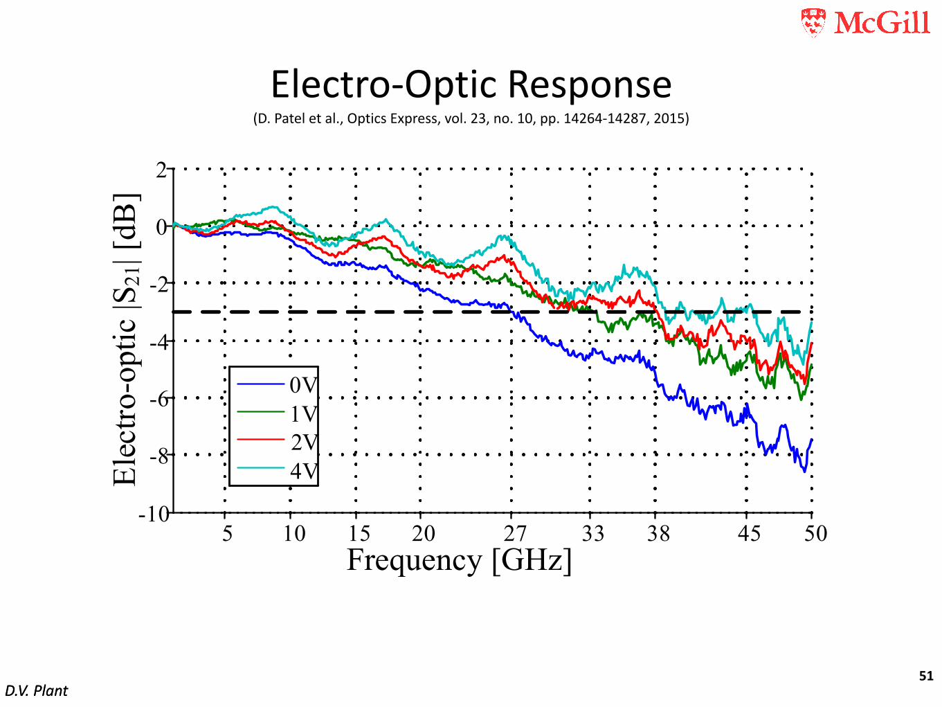
D.V. Plant
Electro-‐Optic Response(D. Patel et al., Optics Express, vol. 23, no. 10, pp. 14264-‐14287, 2015)
5 10 15 20 27 33 38 45 50-10
-8
-6
-4
-2
0
2
Frequency [GHz]
Elec
tro-o
ptic
|S21
| [dB
]
0V1V2V4V
51D.V. Plant

D.V. Plant
OOK Modulation With Passive Pre-‐emphasis(D. Patel et al., Optics Express, vol. 23, no. 10, pp. 14264-‐14287, 2015)
60 Gbps; ER = 5.9 64 Gbps; ER = 5.7
70 Gbps; ER = 5.5 72 Gbps; ER = 3.752
D.V. Plant

D.V. Plant
160 200 240 280 320 360
10-4
10-3
10-2
10-1
Bit Rate [Gbits/s]
BER
BER threshold of SD-FEC: 2×10œ2
BER threshold of HD-FEC: 3.8×10œ3
6 bits/symb, DPœPAM4 + 4PM
250 Gb/swith 12% OH
280 Gb/swith 25% OH
a)
6 Bits/Symbol DP-‐PAM4+4PM (M. Chagnon et al., Optical Fiber Communications (OFC) Conference, post-‐deadline paper Th5B.2, 2015)
53
5658.4
49423528Symbol Rate [Gsymbols/s]
22 10 −×
33.8 10 −×270 Gb/s with 12 % OH
250 Gb/s with 12 % OH
280 Gb/s with 25 % OH

© 2015 L. ChrostowskiSi-EPIC CREATE
Optical Switch
54
Design
Fabless model (CMC Si-EPIC MPW)
Fabricated at IME A*STAR with the CMC-IME process
8
1 mm
0.25
mm
2x2 switching element
Fibre Array Optical I/O
4x4 crossbar switch
“A 4x4 fully non-blocking switch on SOI based on interferometric thermo-optic phase shifters”, David Patel*, Venkat Veerasubramanian, Samir Ghosh, Wei Shi, Alireza Samani, Qiuhang Zhong, and David V. Plant, OIC 2014
Design
2x2 Thermal MZI building block
Single drive
Theoretically: cross-state with no phase–shift,
and bar-state with 𝜋 phase shift
For 100 µm phase shifters:
𝜋 phase shift with Δ𝑇 ≈ 42 oC
10
Δ𝜙 = 0
Δ𝜙 = 𝜋
220 µm
25 µm
20 30 40 50 60 70 80-40
-30
-20
-10
0Single Drive MZI Heater (100 µm)
Sim
ulat
ed T
rans
mis
sion
[dB
]
Temperature [°C]
Output 1Output 2
𝜙2 = 2𝜋𝜆0
𝑛𝑒𝑒𝑒2 𝑇0 𝐿2
𝑂1𝑂2 = 1 − 𝜖 𝑗 𝜖
𝑗 𝜖 1 − 𝜖𝑒−𝑗𝜙1 0
0 𝑒−𝑗𝜙21 − 𝜖 𝑗 𝜖𝑗 𝜖 1 − 𝜖
𝐼𝑛1𝐼𝑛2
𝜙1 = 2𝜋𝜆0
𝑛𝑒𝑒𝑒1 𝑇0 + 𝜕𝑛𝜕𝑇 𝑇 − 𝑇0 𝐿1
𝜖:𝐶𝑙𝐶𝐶𝑙𝑒𝐶 𝐶𝑙𝑝𝑒𝐶 𝑠𝐶𝑙𝑠𝑠𝑠𝑠𝑛𝑙 𝐶𝑟𝑠𝑠𝑙
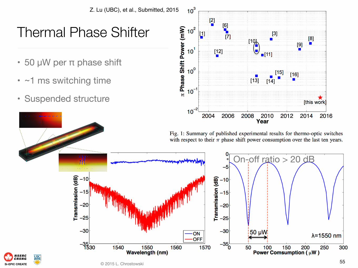
© 2015 L. ChrostowskiSi-EPIC CREATE
Thermal Phase Shifter
• 50 µW per π phase shift
• ~1 ms switching time
• Suspended structure
55
• On-off ratio > 20 dB
IEEE PHOTONICS TECHNOLOGY LETTERS 3
1530 1540 1550 1560 1570−35
−30
−25
−20
−15
−10
−5
0
Wavelength (nm)
Tran
smis
sion
(dB
)
ONOFF
(a)
0 50 100 150 200 250 300−35
−30
−25
−20
−15
−10
−5
0
Power Comsumption ( µW )
Tran
smis
sion
(dB
)
50 µW λ=1550 nm
(b)
−2 0 2 4 6 8 10 12−0.2
0
0.2
0.4
0.6
0.8
1
Time (ms)
Nor
mal
ized
Tra
nsm
issi
on
780 µs 500 µs
(c)
Fig. 5: Measurement results for device 6. (a) optical transmission at switchingON and OFF states; (b) transmission at 1550 nm as a function of tuning power;(c) time-domain response at 1550 nm.
The measured resistances of the metal heaters are approxi-mately 380 for all devices. Figure 5(a) presents the TE modetransmission at switching ON and OFF states for device 6. Forthe same device, the measured insertion loss is 3.3 dB at 1550nm, which is mainly due to the round-trip propagation loss ofthe 4.27 mm long phase arms and the waveguide bends. Asshown in Fig. 5(b), at 1550 nm the measured power to switchfrom the maximum to minimum transmission is 50 µW, andthe switching extinction ratio is 26 dB. The 10%-90% responsetime for device 6 is 1.28 ms, including a 780 µs rise time anda 500 µs fall time, as shown in Fig. 5(c).
1 2 3 4 5 6 7 8 9 10 1110−2
10−1
100
101
102
Number of waveguides N
Pow
er c
onsu
mpt
ion
(mW
)
With suspended structuresWithout suspended structures
35×
(a)
1 2 3 4 5 6 7 8 9 10 110
0.2
0.4
0.6
0.8
1
1.2
Number of waveguides N
Rep
onse
Tim
e (m
S)
With suspended structuresWithout suspended structures 6×
(b)Fig. 6: Performance comparison of the test devices. (a) Switching power; (b)response time. The dash lines are fitting curves for measurement results.
For comparison, measurement results for all test devicesare shown in Figs. 6(a) and 6(b). As shown in Fig. 6(a), thepower consumption of the devices significantly decreases withincreasing number of waveguides, N , which is in good agree-ment with (1). When comparing the devices with suspendedstructures to those without, we found that the suspendedstructures can reduce the power consumption by approximately35 times. As shown in Fig. 6(b), increasing the number ofwaveguides does not significantly influence the response timeof the devices. However, the response time of the devices withsuspended structures is approximately 6 times slower than thatof those without. For thermally isolated structures there is a
tradeoff between efficiency and response time [9], however,the improvement in efficiency (35) is much more dramaticthan the degradation of response time (6).
IV. DISCUSSION
In this section, we show that improvements can be madeto further reduce the power consumption of our switches.Figure 7 shows a 3D temperature distribution in the suspendedarm of device 6 when a power of 50 µW is supplied tothe heater, which is obtained through a 3D heat transfersimulation [23]. The two ends of the arm and the small supportbridges between the isolation trenches are found to be themajor outlets of the leaking heat. As a result, having a longersuspended arm and fewer bridges may improve the thermalisolation, and thus further reduce the power consumption ofour switches. Additionally, thermal isolation can be appliedto the second arm of the interferometer to further reduce thethermal crosstalk between the arms.
[°C]
Fig. 7: 3D heat transfer simulation for the suspended arm of device 6. The bluearrows indicate the heat flux. The size of the arrows indicates the magnitudeof the heat flux.
V. CONCLUSION
In this work, we demonstrated a silicon photonicthermo-optic switch with an extremely low power consump-tion of 50 µW, which is realized by using a Michelsoninterferometer configuration with a suspended phase arm anddensely folded waveguides. To the best of our knowledge,this is the lowest power consumption reported for a siliconphotonic thermo-optic switch. The device shows an extinctionratio of 26 dB at 1550 nm for the TE mode, and a 10%-90%response time of 1.28 ms.
ACKNOWLEDGMENT
We acknowledge the financial support from the Natural Sci-ences and Engineering Research Council of Canada (NSERC),particularly the SiEPIC program. Zeqin Lu appreciates theChina Scholarship Council (CSC) for financial support ofhis research project. We would like to thank Miguel Guillen
Z. Lu (UBC), et al., Submitted, 2015

Polarization dependence and management
• High index contrast waveguides are highly birefringent
56
Polarization diversity Requires a polarization splitter
& rotator
Optical Input Polarization
splitter
Photonic circuit
Photonic circuit
TE + TMTE
TM
Polarization rotator
TE
TE
Poon Group (www.photon.utoronto.ca)
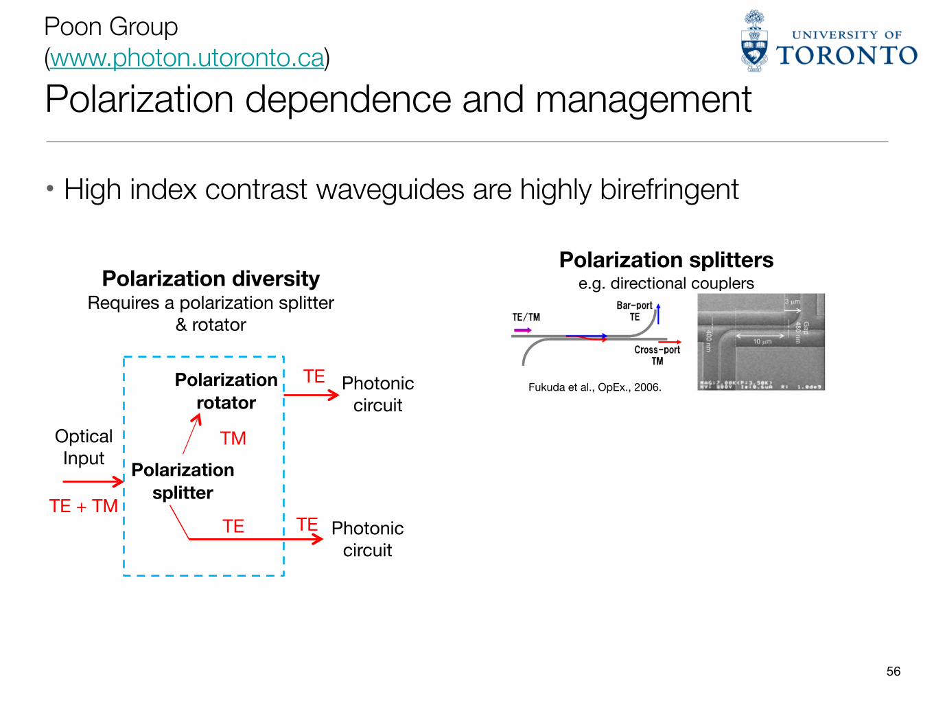
Polarization dependence and management
• High index contrast waveguides are highly birefringent
56
Polarization diversity Requires a polarization splitter
& rotator
Optical Input Polarization
splitter
Photonic circuit
Photonic circuit
TE + TMTE
TM
Polarization rotator
TE
TE
Polarization splitters e.g. directional couplers
Fukuda et al., OpEx., 2006.
Polarization rotators (TM0→TE0) Requires extra processing steps, overlays, or high aspect ratio features
D. Vermeulen et al., GFP, 2010. Barwicz et al.
Nat. Photon. 2007.L. Chen et al., Opt. Lett. 2011.
time, the SiN required for the both is deposited at the same time.The patterns corresponding to the two layers are registered in twodistinct hard masks on top of the SiN, and successive etches andhard-mask removals are applied. This fabrication process isdescribed in more detail in the Methods section.
The optical performance of the fabricated polarization-transparent OADF is presented in Fig. 4 for 40 randomly chosenpolarization states at every wavelength. In addition, independentlyacquired responses of the two polarization eigenstates are overlaidin colour. An extraordinarily low polarization-dependent loss(PDL) with a mean of 1.0 dB and a standard deviation acrossthe spectrum of 0.45 dB is achieved. Of this PDL, 0.3 dB is dueto the optical characterization scheme, which is described inthe Methods section. The measured polarization-transparentbandwidth exceeds 60 nm. In Fig. 4, the PDL is the verticaldistance between the blue and the red curves. Without thepolarization diversity scheme, the underlying microrings wouldshow a spectral misalignment of several nanometres between theresponses of the two polarization eigenstates. Here, the spectralmisalignment is negligible. Defining a misalignment figure ofmerit as the free spectral range of a resonator (20 nm in thiswork) divided by the spectral misalignment, we obtain, withoutany postfabrication trimming, 1,180 for the drop port and 540for the through port. These remaining spectral misalignmentscorrespond to slight differences in resonant frequency between thetwo, nominally identical, multistage microring filters in theOADF. The resonant frequencies are controlled at fabricationthrough the average ring-waveguide width of each microring. Thethrough-port spectral misalignment corresponds to a remarkablerelative control of the average ring-waveguide widths of all 18microrings of the OADF to 0.15 nm, and the drop-port spectralmisalignment corresponds to a relative control of the averagering-waveguide widths of the 6 microrings of the first stages ofthe two filters to 0.07 nm. This relative dimensional control wasachieved through precise adjustments of the electron beam(e-beam) exposure dose of the various microrings and a tailorede-beam writing strategy17. Relative control is to be distinguishedfrom absolute dimensional control, which is impossible to achieveto such an extent.
The fabricated polarization-transparent OADF shows aremarkable through-port extinction of more than 32 dB and adrop loss of no more than 2 dB. Its bandwidth spans 50 GHz(0.40 nm), its free spectral range reaches 2.5 THz (20 nm), and itallows a minimum channel spacing of 130 GHz (1.05 nm). Thetransmission between the add and the through port is not shown,but is almost identical to the transmission between the input andthe drop port. The polarization sensitivity on the bottom of the
through-port response is of no consequence as it is below the30-dB extinction required in OADFs. The spectral oscillations,particularly visible off-resonance in the through-port response,are due to a shortcoming of the scanning electron-beamlithography system that was used. This is explained in greaterdetail in the Supplementary Information.
The demonstration of integrated polarization diversity opensa path for the construction of polarization-transparent SCmicrophotonic circuits from arbitrarily polarization-sensitive SCmicrophotonic components. The efficacy of this approach wastested rigorously by realizing the first polarization-transparentOADF from polarization-sensitive SC microring resonators.The resulting SC microphotonic circuit is, to our knowledge,the most complex achieved to date. It demonstrates almostcomplete elimination of polarization sensitivity over the
a
c d e f g h i
b
100 µmIn
AddDrop
ThroughCrossing
SiN
Cr Ni
80 nm
970 nm
In
Add Drop
Through
In
AddDrop
Through
Figure 3 Fabricated polarization-transparent OADF. a, Electron micrograph of the central part of a fabricated polarization-transparent OADF. The PSRs are not
shown and extend to the left and the right of the micrograph. The picture was assembled from six successive micrographs and the greyscale was inverted to makethe fine lines readable when printed. b, Electron micrograph of the onset of a polarization splitter. The finest features show an aspect ratio of more than 12:1.c– i, Illustration of the novel fabrication technique used to create the bilevel structures. The technique is described in detail in the Methods section.
0
–10
–20
–30
–50
–40
Tran
smis
sion
(dB)
Wavelength (nm)1,551 1,5541,5531,552 1,555
Input TE
Input TM
Random
Drop port
Through port
Figure 4 Spectral response of a fabricated polarization-transparent OADFfor 40 randomly chosen polarization states at each wavelength. The spectral
responses for the two polarization eigenstates are overlaid in blue and red.A remarkably low polarization-dependent loss (the vertical distance between theresponses of the two eigenstates) with a mean of 1.0 dB and standard deviationof 0.45 dB is demonstrated. Of the shown polarization-dependent loss, 0.3 dB isdue to the optical characterization setup. The polarization-transparent operation
was designed to exceed a 300-nm bandwidth and was confirmed over the60-nm bandwidth measured. This is achieved without any postfabricationtrimming and while maintaining spectacular filter performance. The shape ofthe spectral response below the 230 dB line is of no consequence.
LETTERS
nature photonics | VOL 1 | JANUARY 2007 | www.nature.com/naturephotonics 59
Poon Group (www.photon.utoronto.ca)
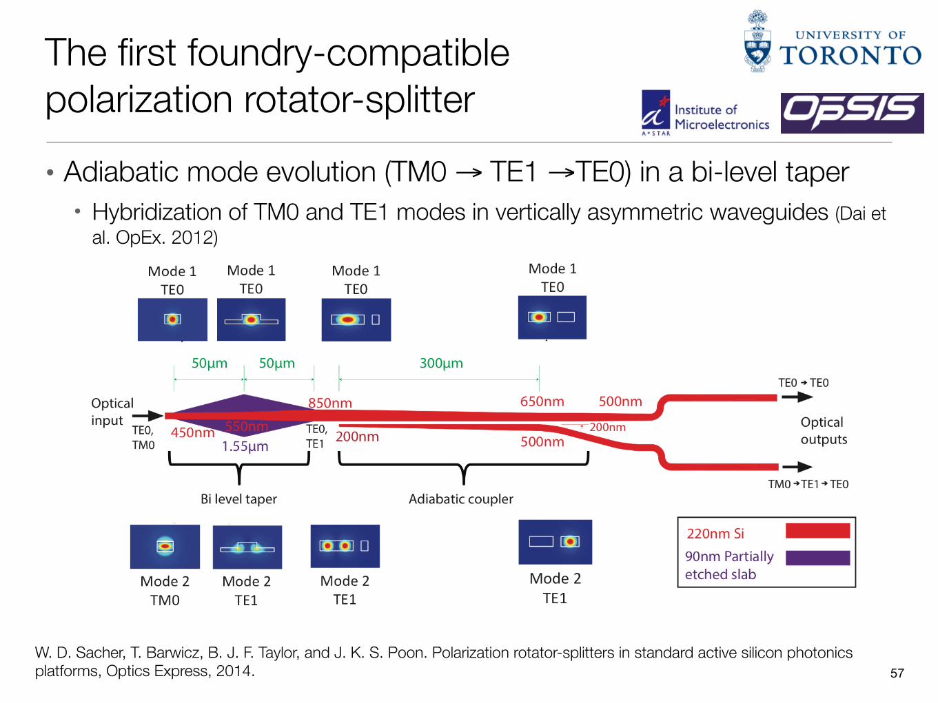
The first foundry-compatible polarization rotator-splitter
• Adiabatic mode evolution (TM0 → TE1 →TE0) in a bi-level taper • Hybridization of TM0 and TE1 modes in vertically asymmetric waveguides (Dai et
al. OpEx. 2012)
57W. D. Sacher, T. Barwicz, B. J. F. Taylor, and J. K. S. Poon. Polarization rotator-splitters in standard active silicon photonics platforms, Optics Express, 2014.
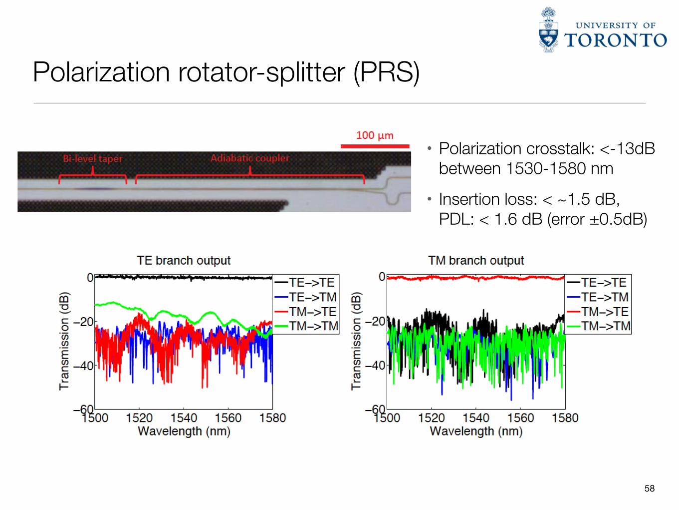
• Polarization crosstalk: <-13dB between 1530-1580 nm
• Insertion loss: < ~1.5 dB, PDL: < 1.6 dB (error ±0.5dB)
58
Polarization rotator-splitter (PRS)

Polarization rotator splitter (PRS) with directional coupler filters
59
• Polarization crosstalk: <-22dB between 1500-1580 nm
• Insertion loss: < ~2.3 dB, PDL: < 1.9 dB (error ±0.5dB)

A simple polarization controller
60
TE input
The bi-level PRS is fully compatible with standard active Si platforms.

SiEPIC ProgramSi-EPIC CREATE
Filters for Datacomm
• Ring resonators• Passive optical filters implement in silicon photonics• Optical data transmission experiments
61
and 1(c), we find the optimum radius for a microring to be 8 µm using simulated losses and 9 µm using measured losses. Fromthe simulated results, for MRRs with 8 µm radii, 10 channels with a 150 GHz channel spacing can fit into an FSR of 12.4 nm.By using 2nd-order MRRs, the channel count can be increased to 25 with a 62.5 GHz channel spacing. The calculated FWHMvalues for the MRRs and 2nd-order MRRs were 29 GHz and 40 GHz, respectively.
III. CROSSTALK PENALTY MEASUREMENTS OF MRR AND 2ND-ORDER MRR 2-CHANNEL DEMUXS
We used wavelength tunable MRR and 2nd-order MRR based DeMUXs to measure the crosstalk penalty between two adjacentchannels. The devices were fabricated with 8 µm radii and doped silicon heaters were used for wavelength tuning. The measuredspectra of the fabricated devices are shown in Figs. 2(a)(i) and 2(a)(ii). The measured average FWHM of the MRRs was 33GHz and of the 2nd-order the MRRs was 41 GHz, which are close to the values calculated in the previous section.
DUT 2ch2ch1
VOA
ch1 ch2
DUT 1(i) (ii)
MZM 2
PPG 2
MZM 1
PPG 1
EDFAOTF
(4 nm)
3 dB Coupler
PDBERT
λ1
λ2
ch1
ch2ch1
ch2DUT 1,2
(iii)
thruthru
(a) (b) (c)
Fig. 2: (a) (i) MRR DeMUX and the measured spectra for ch1 and ch2, (ii) 2nd-order MRR DeMUX and the measured spectrafor ch1 and ch2, and (iii) the experimental setup for measuring crosstalk. (b) Measured BERs as a function of received opticalpower at the PD. (c) Crosstalk penalties for a BER of 1012 at 25 Gb/s.
The experimental setup is shown in Fig. 2(a)(iii). Two independent pulse pattern generators (PPGs), outputting non-return-to-zero 231-1 pseudo random binary sequences at 25 Gb/s, were used to modulate two commercial LiNbO3 Mach-Zehndermodulators (MZMs). The optical power in both channels was kept equal by adjusting the output power of the two lasers used.The signal out of the device-under-test (DUT) was amplifed using an erbium-doped fiber amplifier (EDFA) and was filtered usingan optical tunable filter (OTF). A variable optical attenuator (VOA) was used to control received power at the photo-detector(PD). The bit-error-ratio (BER) of ch1 or ch2 was measured after tuning the channel spacing of the DeMUXs.
The BER versus received power for several channel spacings is shown in Fig. 2(b). We extract the crosstalk power penalty asa function of the channel spacing by performing a linear extrapolation and finding the power corresponding to a BER of 1012.The results are shown in Fig. 2(c). Based on the BER, the crosstalk appears to be negligible at channel spacings of 150 GHzfor MRRs and 100 GHz for 2nd-order MRRs. Therefore, the crosstalk penalties shown in Fig. 2(c) are measured relative to thesechannel spacings. For a DeMUX, after the first channel is dropped, the crosstalk from that channel to subsequently droppedchannels is reduced. Hence, the crosstalk power penalty measured for ch2 of the MRR DeMUX is lower than that for ch1. Forch1, assuming a maximum permissible crosstalk penalty of 0.2 dB, the minimum channel spacing using MRRs is 72 GHz, whichcorresponds to 21 channels. Using 2nd-order MRRs, the minimum channel spacing is 62 GHz, which corresponds to 25 channels.Therefore, at a data rate of 25 Gb/s/channel, by using an MRR DeMUX the link capacity could be as high as 525 Gb/s and couldbe increased up to 625 Gb/s by using a 2nd-order MRR DeMUX.
IV. CONCLUSION
For a given SOI photonics technology platform, the MRR’s finesse, which is affected by the waveguide bend loss, determinesthe MRR radius that maximizes the WDM channel count. By measuring the crosstalk power penalty, we showed that higher linkdata capacities can be obtained by using a 2nd-order MRR DeMUX as compared to using an MRR DeMUX.
ACKNOWLEDGMENTS
The authors would like to thank CMC Microsystems and NSERC for financial support. The authors also thank AnritsuCorporation for the use of their MP1800A Signal Quality Analyzer and Dr. Roberto Rosales for help with the equipment.
REFERENCES[1] A. V. Krishnamoorthy et al.,“Computer systems based on silicon photonic interconnects,” Proc. IEEE, vol. 97, no. 7, pp. 1337-1361, 2009.[2] N. Ophir et al., “Silicon photonic microring links for high-bandwidth-density, low-power chip I/O,” IEEE Micro., vol. 33, no. 1, pp. 54-67, Jan./Feb, 2013.[3] K. Padmaraju et al.,“Intermodulation crosstalk characteristics of WDM silicon microring modulators,” IEEE Photon. Technol. Lett., vol. 26, no. 14, pp.
1478-1481, 2014.[4] K. Preston et al., “Performance guidelines for WDM interconnects based on silicon microring resonators,” in Proc. CLEO, May 2011, pp. 1-2.[5] W. R. McKinnon et al., “Extracting coupling and loss coefficients from a ring resonator,” Opt. Exp., vol. 17, no. 21, pp. 18971-18982, 2009.[6] B. E. Little et al., “Microring resonator channel dropping filters,” J. Lightw. Technol., vol. 15, no. 6, pp. 998-1005, 1997.[7] J. K. S. Poon et al., “Matrix Analysis of Microring Coupled-Resonator Optical Waveguides,” Opt. Exp., vol. 12, no. 1, pp. 90-103, 2004.
Crosstalk Limitations of Microring-Resonator BasedWDM Demultiplexers on SOI
Hasitha Jayatilleka, Michael Caverley, Nicolas A. F. Jaeger, Sudip Shekhar, and Lukas ChrostowskiDepartment of Electrical and Computer Engineering, University of British Columbia
2332 Main Mall, Vancouver, BC V6T 1Z4, [email protected]
AbstractWe determine the radius that maximizes the channel count for microring WDM demultiplexers. By measuring crosstalk, we
show channel spacing requirements and calculate maximum aggregate data rates for microring and second-order microring basedWDM links.
I. INTRODUCTION
Due to their compact size and low power consumption, modulators, wavelength filters, and switches based on microring-resonators (MRRs) offer attractive solutions for wavelength-division multiplexed (WDM) links on silicon photonics platforms [1].For a high-speed serial-link using MRRs [2], the number of WDM channels is limited by the inter-modulation crosstalk at thetransmit end [3]. At the receive end, the channel count is limited by the inter-channel crosstalk of the demultiplexer (DeMUX)[4], which depends on the channel spacing and the shape of the MRR’s filter response.
In this paper, we show the optimal design of MRR and 2nd-order MRR filters for wavelength DeMUX applications for agiven photonics platform. Given a maximum tolerable insertion loss (IL) and crosstalk, we obtain the maximum WDM channelcount by finding the MRR radius corresponding to the maximum finesse. We then measure the crosstalk penalty as a function ofthe channel spacing at a data rate of 25 Gb/s for both an MRR DeMUX and a 2nd-order MRR DeMUX. Based on our findings,we evaluate the crosstalk-limited maximum data capacities for WDM links using MRRs and 2nd-order MRRs.
II. DESIGN CONSIDERATIONS FOR MRR AND 2ND-ORDER MRR DEMUXS
In this work, we used the IME silicon-on-insulator (SOI) photonics platform with 248 nm photolithography. We used ribwaveguides with a height of 220 nm, a slab height of 90 nm, and a width of 500 nm. All of the devices used straight buswaveguides, with equal ring-to-bus waveguide gaps at the through- and drop-ports, to couple light into and out of MRRs. The2nd-order MRR designs had equal radii for both rings.
As the radius of an MRR is reduced, it’s free-spectral-range (FSR) increases, allowing more channels to fit within one FSR.However, the radiation loss also increases, which causes the MRR’s filter response to broaden, thus increasing the inter-channelcrosstalk. Therefore, the channel count is maximized when the finesse (F), which is defined as F = FSR/FWHM, where FWHMis the full-width-at-half-maximum bandwidth, reaches a maximum value. Figure 1(a) shows the simulated and measured bendlosses for MRRs with different radii. Lumerical MODE Solutions was used to obtain the simulated values. The measured bendloss values are extracted from fabricated devices using the measured through- and drop-port spectra [5]. The measured lossesare normalized to the loss of an undoped MRR with a 15 µm radius, assuming that the total loss at this radius is equal to thatof a straight waveguide. The measured waveguide loss in the 15 µm MRR is about 2 dB/cm. The measured additional loss dueto doping is about 6 dB/cm. For a nominal slab height of 90 nm, the difference between the measured and the simulated bendlosses significantly increases as the radius is reduced. This is likely a result of the variations in fabrication, as the the measureddata closely matches with simulated bend losses for a slab height of 95.5 nm.
Constraining the maximum drop-port IL to 0.75 dB, we designed both MRRs and 2nd-order MRRs by finding the requiredcoupling values that meet this criteria [6, 7]. The calculated finesse of an MRR as a function of the radius is shown in Fig.1(b). The maximum WDM channel count for MRRs and 2nd-order MRRs is shown in Fig. 1(c), which was calculated by findingthe maximum number of channels that can fit in one FSR while maintaining a crosstalk of less than −15 dB. From Figs. 1(b)
(a) (b) (c)
Fig. 1: (a) Simulated and measured bend loss, and (b) finesse, as a function of MRR radius. (c) Crosstalk-limited maximumchannel capacity for MRR and 2nd-order MRR DeMUXs.
IEEE OIC 2015

• Add/drop multiplexer for WDM communication• Suppression of co-directional coupling – waveguides with different widths• Principle: efficient coupling requires phase match
• Contra-directional coupling – Periodic perturbation the waveguides
SiEPIC ProgramSi-EPIC CREATE
indices are calculated using the FDTD mode solutionswith 5 nm meshes.
The transmissionThe
1510 1515 1520 1525 1530−45
−40
−35
−30
−25
−20
−15
Wavelength [nm]
Po
we
r [d
Bm
]
Drop
Through
βa
+ + β
a
− βa
+ + β
b
−
Fig. 2. One-column figure set with the figure environ-ment.
Fig. 3. One-column figure set with the figure environ-ment.
Sample code for the preamble is as follows:
\documentclass[10pt,twocolumn]article\usepackageol%% Figures should be placed in body
%% of manuscript and%% sized appropriately.
The command \twocolumn[...] must be placedaround the titlepage elements in the two-column option.Note that proper figure, table, and caption environmentsshould be used (see samples below).
Displayed equations may be the most problematicfor two-column display. Optics Letters equations are usu-ally set in one column; breaks and alignment shouldbring out the structure of the math:
κ =ω
4
!!ψ∗
a(x, y) · ε1(x, y) ψb(x, y) dx dy (1)
Photonic bandgap
λ =2λ2
0
π(ng,a + ng,b)| κ | (2)
β = β1 − β2 − mλ
Λ= 0 (3)
Ex,y =1
2(1 + jα) (Gx,y − γ)Ex,y
+ κEx,y (t − τ) exp (−jΩx,yτ)
+ (βspN)1/2ξx,y. (4)
Ex,y =1
2(1 + jα) (Gx,y − γ)Ex,y
+ κEx,y (t − τ) exp (−jΩx,yτ)
+ (βspN)1/2ξx,y. (5)
Use standard LaTeX or AMSTeX environ-ments. For equations that must span two columns,it is possible to use a float environment, e.g.,\beginfigure*...\endfigure*. Such an en-vironment will not interfere with figure or tablenumbering (which is controlled by the caption), butit will cause equations to float, often with unwantedconsequences.
Figures should be set to one-column size (∼8.3 cm)whenever possible; tables should also be set to one col-umn whenever possible, but tables with more than fivecolumns will probably need to be set to two columns. Fortwo-column layout, figures and tables can be set acrossboth columns with the alternate figure and table environ-ment commands \beginfigure*...\endfigure*instead of \beginfigure...\endfigure. Note thattables are typeset and cannot be reduced in size like art,which may require more space than in the submittedpaper.
Sample figure environment:
\beginfigure[htb]\centerline
\includegraphics[width=8.3cm]richardson-f1.eps\captionSample figure.\endfigure
References callouts are now formatted with the citepackage, which produces bracketed reference style (e.g.,[1]). For online callouts, e.g., see [1], the words “Ref.”and “Refs.” are not required.
Before submitting, authors who use BibTeX shouldfirst run BibTeX, then paste the contents of the outputfile *.bbl into the *.tex manuscript file. Our electronicsubmissions system cannot process BibTeX directly.
The following files are included in this distribu-
tion:
• OLpagelength.tex Template and instructions
• ol2.sty Style file
• ol.bst BibTeX style file for short-form citations(as published)
2
Contra-directional couplers
62
WDM Input
Wei Shi, SPIE 2014

SiEPIC ProgramSi-EPIC CREATE
Contra-directional couplers
63
High-Speed Data Transmission Through SiliconContra-Directional Grating Coupler Optical
Add-Drop Multiplexers
Michael Caverley, Robert Boeck, Lukas Chrostowski and Nicolas A. F. JaegerDepartment of Electrical and Computer Engineering, University of British Columbia,
2332 Main Mall, Vancouver, British Columbia, V6T 1Z4, Canada
Abstract: We demonstrate 12.5 Gbit/s data transmission through a silicon contra-directionalgrating coupler optical add-drop multiplexer while signals are being simultaneously addedand dropped at the same wavelength.OCIS codes: (230.1480) Bragg reflectors; (130.7408) Wavelength filtering devices
1. IntroductionSilicon photonics optical interconnects using wavelength-division multiplexing (WDM) are potential solutions to theincreasing demand for high data rates. Silicon contra-directional couplers (contra-DCs), using gratings, have beeninvestigated for use as add-drop filters in on-chip WDM systems [1–6]. Compared to ring resonator based filters,contra-DC ones do not have periodic spectral responses [4], however, they typically have larger bandwidths makingthem suitable for coarse WDM (CWDM) applications [5]. In this work, we demonstrate data transmission at 12.5Gbit/s through a silicon-on-insulator contra-DC optical add-drop multiplexer (OADM).
2. Device DescriptionThe contra-DC OADM was fabricated using electron beam lithography at the University of Washington [7]. Thecontra-DC was formed by adding side-wall corrugations to the strip waveguides in the coupling region. Anti-reflectiongratings, that are out of phase with the corrugations in the coupling region, were also added to suppress intra-waveguideBragg reflections [5]. The waveguides had a height of 220 nm and there was an oxide cladding. Figure 1(a) shows adiagram of the device with the various dimensions and ports labeled. Figure 1(b) shows the spectral response of thecontra-DC OADM. The through port stopband is centered at a wavelength of 1536.4 nm and has a through port sup-pression of about 20 dB. The drop port response has a 3 dB bandwidth of about 4.5 nm and has a sidelobe suppressionof about 4.4 dB, which was measured as the difference between the power at 1536.4 nm and the maximum sidelobepower. The sidelobe suppression can be increased by using apodization [6]. The filter also has some co-directionalcoupling from the input port to the add port. The amount of co-directional power coupling is about 3% in the regionnear the stopband.
450 nm
550 nm
30 nm
40 nm 312 nm
140 nm
Input
Drop
Through
Add
156 µm
(b) (a)
Fig. 1. (a) Diagram of the contra-DC OADM showing a zoom-in of the coupling region (similar to [8]) and (b) measuredspectral response of the filter.
3. Experimental ResultsTo characterize the OADM’s performance, we used an experimental setup similar to the one in [9] but with twoseparate optical paths, the input-to-drop path and the add-to-through path. Figure 2 shows the measured eye diagramsfor data transmitted at 12.5 Gbit/s through the contra-DC OADM when the data is being dropped only, added only,and simultaneously added and dropped. Figures 2(a) and 2(d) show eye diagrams of the data from the MZI modulatorsgoing to the input port and add port of the OADM, respectively, so that the signal quality at the output of the systemcan be compared to the signal quality of the data which is being input to the OADM. Figure 2(b) shows that whenthe OADM is dropping a signal only, then there is minimal distortion in the signal. However, when a signal is beingadded and dropped at the same time [Fig. 2(c)], then the signal quality of the dropped signal is reduced and the eyeis less open. Figures 2(e) and 2(f) show similar behavior for the signal being added. Our results show that despitereduced signal qualities, the eyes remained open for both the added and dropped signals, demonstrating successfuldata transmission at 12.5 Gbit/s through this contra-DC OADM.
(a) Input Drop
Through
Add
Input Drop
Through Add
Input Drop
Through Add
Input Drop
Through Add
(b) (c)
(d) (e) (f)
MZI Modulator 1
MZI Modulator 2
Fig. 2. Measured eye diagram of: (a) data from the MZI modulator prior to entering the filter’s input port; (b) data passingfrom the input port to the drop port when the device is only dropping the signal; (c) data passing from the input port to thedrop port while another signal is being added; (d) data from the MZI modulator prior to entering the filter’s add port; (e) datapassing from the add port to the through port when the device is only adding a signal; (f) data passing from the add port tothe through port while another signal is being dropped.
4. SummaryWe have demonstrated successful data transmission at 12.5 Gbit/s through a contra-DC OADM when it is only drop-ping a signal, only adding a signal, and simultaneously adding and dropping signals at the same wavelength.AcknowledgmentsWe acknowledge the Natural Sciences and Engineering Research Council (NSERC) of Canada for their financial sup-port. We also acknowledge CMC Microsystems, Mentor Graphics, and Lumerical Solutions, Inc. We also acknowledgeDr. Wei Shi, Richard Bojko, Yun Wang, Jonas Flueckiger, and Han Yun. Part of this work was conducted at the Univer-sity of Washington Nanofabrication Facility, a member of the NSF National Nanotechnology Infrastructure Network.References
1. D. T. H. Tan, A. Grieco, and Y. Fainman, “Towards 100 channel dense wavelength division multiplexing with 100GHz spacing on silicon,”Opt. Express 22, 10408–10415 (2014).
2. H. Qiu, G. Jiang, T. Hu, H. Shao, P. Yu, J. Yang, and X. Jiang, “FSR-free add-drop filter based on silicon grating-assisted contradirectionalcouplers,” Opt. Lett. 38, 1–3 (2013).
3. K. Ikeda, M. Nezhad, and Y. Fainman, “Wavelength selective coupler with vertical gratings on silicon chip,” Appl. Phys. Lett. 92, 201111(2008).
4. W. Shi, X. Wang, W. Zhang, L. Chrostowski, and N. A. F. Jaeger, “Contradirectional couplers in silicon-on-insulator rib waveguides,” Opt.Lett. 36, 3999–4001 (2011).
5. W. Shi, H. Yun, C. Lin, M. Greenberg, X. Wang, Y. Wang, S. T. Fard, J. Flueckiger, N. A. F. Jaeger, and L. Chrostowski, “Ultra-compact, flat-top demultiplexer using anti-reflection contra-directional couplers for CWDM networks on silicon,” Opt. Express 21, 6733–6738 (2013).
6. W. Shi, H. Yun, C. Lin, J. Flueckiger, N. A. F. Jaeger, and L. Chrostowski, “Coupler-apodized Bragg-grating add-drop filter,” Opt. Lett. 38,3068–3070 (2013).
7. R. J. Bojko, J. Li, L. He, T. Baehr-Jones, M. Hochberg, and Y. Aida, “Electron beam lithography writing strategies for low loss, highconfinement silicon optical waveguides,” J. Vac. Sci. Technol. B 29, 06F309 (2011).
8. R. Boeck, W. Shi, L. Chrostowski, and N. A. F. Jaeger, “FSR-eliminated vernier racetrack resonators using grating-assisted couplers,” IEEEPhot. J. 5, 2202511 (2013).
9. A. Melloni, M. Martinelli, G. Cusmai, and R. Siano, “Experimental evaluation of ring resonator filters impact on the bit error rate in nonreturn to zero transmission systems,” Opt. Commun. 234, 211–216 (2004).
M. Caverley, R. Boeck, L. Chrostowski, N.A.F. Jaeger, “High-Speed Data Transmission Through Silicon Contra-Directional Grating Coupler Optical Add-Drop Multiplexers”, CLEO 2015
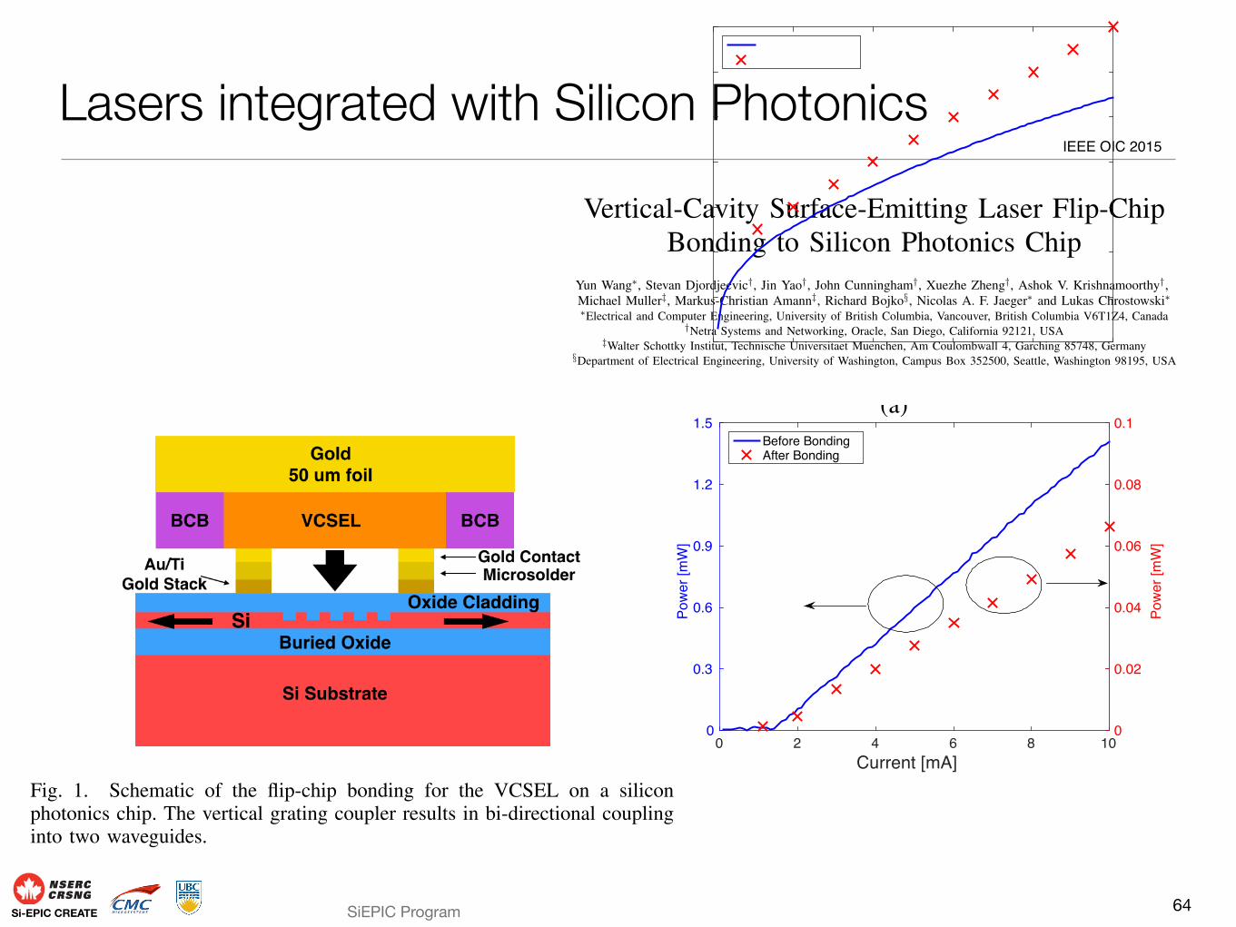
SiEPIC ProgramSi-EPIC CREATE
Lasers integrated with Silicon Photonics
64
Vertical-Cavity Surface-Emitting Laser Flip-ChipBonding to Silicon Photonics Chip
Yun Wang, Stevan Djordjecvic†, Jin Yao†, John Cunningham†, Xuezhe Zheng†, Ashok V. Krishnamoorthy†,Michael Muller‡, Markus-Christian Amann‡, Richard Bojko§, Nicolas A. F. Jaeger and Lukas ChrostowskiElectrical and Computer Engineering, University of British Columbia, Vancouver, British Columbia V6T1Z4, Canada
†Netra Systems and Networking, Oracle, San Diego, California 92121, USA‡Walter Schottky Institut, Technische Universitaet Muenchen, Am Coulombwall 4, Garching 85748, Germany
§Department of Electrical Engineering, University of Washington, Campus Box 352500, Seattle, Washington 98195, USA
Abstract—We demonstrate the integration of vertical-cavity
surface-emitting lasers (VCSELs) with silicon photonics chip
using flip-chip bonding technique, with bidirectional vertical-
coupled grating coupler for light coupling.
I. INTRODUCTION
One of the most important remaining issues faced by thesilicon photonics community is the on-chip laser source. Po-tential solutions fall into two categories. One is heterogeneousintegration by direct wafer bonding or epitaxial growth, theother is hybrid integration of silicon photonics chips withIII-V epitaxy on laser chips. Heterogeneous integration haschallenges related to crystal properties and fabrication process,whereas the hybrid solution can integrate the optimized siliconphotonics chips to best in breed III-V epitaxial laser chips. Dueto their surface-normal emission, VCSELs are of great interestfor hybrid integration with grating-based off chip couplers insilicon, enabling simple, direct bonding schemes. Enormousprogress has been made in VCSEL technology in the past twodecades, with various successful attempts at hybrid integrationof VCSELs to various carrier substrates [1], [2]. The flip-chip bonding technique has been used to bond both singleVCSEL [1] and VCSEL arrays to CMOS chips [3]. However,flip-chip bonding of VCSELs with silicon photonics chips ismore challenging than the bonding of VCSELs with CMOSchips. High alignment accuracy is required during the bondingprocess as the output from the VCSEL needs to be preciselyaligned to the vertical grating coupler on the silicon photonicschip. In this paper, we demonstrate the integration a VCSEL[4] with silicon photonics chip using the flip-chip bondingtechnique, with custom designed vertical grating couplers asthe input/output interfaces. The schematic of the bondingstructure is shown in Fig. 1.
II. VERTICAL GRATING COUPLER
A vertical grating coupler is required to couple the lightfrom the VCSEL onto the silicon photonics chip. Such verticalgrating couplers have been designed to couple light fromoptical fibers onto silicon photonics chips [5]. However, theexisting vertical grating coupler only couplers light to one sideof the coupler, and normally a maximum coupling efficiencyof 50% applies due the symmetry of the design. The near-field mode size of the VCSEL is smaller than the mode size
Fig. 1. Schematic of the flip-chip bonding for the VCSEL on a siliconphotonics chip. The vertical grating coupler results in bi-directional couplinginto two waveguides.
from an optical fiber. Therefore, a smaller grating coupler isrequired, which makes high-accuracy alignment more difficultto achieve for the bonding process. A bidirectional verticalgrating coupler is designed to couple the light from the VCSELonto the silicon photonics chip. The cross-section along with amicroscopic image of our bidirectional vertical grating coupleris shown in Fig. 2. Our vertical grating coupler was designedfor silicon-on-insulator (SOI) wafer with a 300 nm siliconlayer and a 800 nm buried oxide. A partial etch layer withetch depth of 145 nm was used and the design parametersare shown in Fig. 2(a). As shown in Fig. 1, the output beamfrom the VCSEL get diffracted at the center of the grating andcouples the light equally into the waveguides on both sidesof the grating. Adiabatic tapers were used on both sides ofthe vertical grating coupler to couple the mode from a 6-µmslab mode into a sub-micron silicon-wire waveguide mode.Detuned output grating couplers were connected to both armsof the vertical grating coupler.
III. FABRICATION AND MEASUREMENT
Fabrication of the silicon photonics chip has been doneusing electron beam lithography [6]. Bond pads were designedfor the silicon photonics chip matching the dimensions ofthe VCSEL pads. 4 µm thick gold traces were depositedon the silicon photonics chip to connect the bond padsto corresponding probe pads far away from the bond pads
IEEE OIC 2015
(a)
(b)
Fig. 2. (a) Schematic of the cross-section of the bidirectional vertical gratingcoupler; (b) microscopic image of top view of a bidirectional vertical gratingcoupler.
(Fig. 2(b)). Therefore, when the VCSEL is flip-bonded to thesilicon photonics chip, we can utilize the pads on the siliconphotonics chip to drive the VCSEL. Chips were aligned andbonded using a standard flip-chip bonding process, with athermally cured epoxy layer for adhesion and gold micro-solder pillars for electrical interconnection. A bonding loadof 0.8 kg was used.
The comparison of the V-I and L-I curves of the bondedVCSEL, before and after bonding, are shown in Fig. 3. It canbe seen from Fig. 3(a) that the driving voltages of the VCSELincreased after bonding to the silicon photonics chip, whichis caused primarily by the additional resistance from the padsand metal wires on the silicon photonics chip. Fig. 3(b) showsthe power versus current of the bonded VCSEL, before andafter bonding. The power after bonded was measured using alarge area detector collecting power from two output gratingcouplers connected to the two arms of the bidirectional verticalgrating coupler bonded to the VCSEL. One of the remainingchallenges is the control over the polarization state of theoutput light from the VCSEL. Our vertical grating couplerwas designed for TE polarized light with a polarization modesuppression ratio of 20 dB. Due to the polarization uncertaintyof the VCSEL and the insertion loss from the input and outputgrating couplers, the measured power after bonding was muchlower (by 13.5 dB) than before bonding. Further improvementcan be made using optical feedback from the grating to controlthe polarization of the VCSEL [7].
IV. CONCLUSION
We demonstrate the integration of a VCSEL with a siliconphotonics chip using the high precision flip-chip bondingtechnique. A bidirectional vertical grating coupler is designedto couple the light from the VCSEL onto the silicon photonicschip. The bonded VCSEL was driven using electrodes on thesilicon photonics chip. Light was successfully coupled intosingle-mode rib waveguides.
REFERENCES
[1] A. V. Krishnamoorthy, L. M. F. Chirovsky, W. S. Hobson,R. E. Leibenguth, S. P. Hui, G. J. Zydzik, K. W. Goossen, J. D. Wynn,
Current [mA]0 2 4 6 8 10
Volta
ge [V
]
0.6
0.8
1
1.2
1.4
1.6
1.8
2Before BondingAfter Bonding
(a)
Current [mA]0 2 4 6 8 10
Pow
er [m
W]
0
0.3
0.6
0.9
1.2
1.5
Pow
er [m
W]
0
0.02
0.04
0.06
0.08
0.1Before BondingAfter Bonding
(b)
Fig. 3. (a) Voltage versus current for the VCSEL before and after bondedto the silicon photonics chip; (b) power versus current for the VCSEL beforeand after bonded to the silicon photonics chip. The power after bonded wasmeasured with a large area detector collecting power from two output gratingcouplers connected to the two arms of the bidirectional vertical grating couplerbonded with VCSEL.
B. J. Tseng, J. Lopata et al., “Vertical-cavity surface-emitting lasers flip-chip bonded to gigabit-per-second CMOS circuits,” Photonics Technology
Letters, IEEE, vol. 11, no. 1, pp. 128–130, 1999.[2] H.-J. J. Yeh and J. S. Smith, “Integration of GaAs vertical-cavity surface
emitting laser on Si by substrate removal,” Applied physics letters, vol. 64,no. 12, pp. 1466–1468, 1994.
[3] A. V. Krishnamoorthy, K. W. Goossen, L. M. F. Chirovsky, R. G. Rozier,P. Chandramani, W. S. Hobson, S. P. Hui, J. Lopata, J. A. Walker, andL. A .D’Asaro, “16 x 16 VCSEL array flip-chip bonded to CMOS VLSIcircuit,” Photonics Technology Letters, IEEE, vol. 12, no. 8, pp. 1073–1075, 2000.
[4] W. Hofmann, M. Muller, G. Bohm, M. Ortsiefer, and M.-C. Amann,“1.55-um VCSEL with enhanced modulation bandwidth and temperaturerange,” Photonics Technology Letters, IEEE, vol. 21, no. 13, pp. 923–925,2009.
[5] X. Chen, C. Li, and H. K. Tsang, “Fabrication-tolerant waveguide chirpedgrating coupler for coupling to a perfectly vertical optical fiber,” Photonics
Technology Letters, IEEE, vol. 20, no. 23, pp. 1914–1916, 2008.[6] R. J. Bojko, J. Li, L. He, T. Baehr-Jones, M. Hochberg, and Y. Aida,
“Electron beam lithography writing strategies for low loss, high con-finement silicon optical waveguides,” Journal of Vacuum Science &
Technology B, vol. 29, no. 6, p. 06F309, 2011.[7] S. J. Schablitsky, L. Zhuang, R. C. Shi, and S. Y. Chou, “Controlling
polarization of vertical-cavity surface-emitting lasers using amorphoussilicon subwavelength transmission gratings,” Applied physics letters,vol. 69, no. 1, pp. 7–9, 1996.

© 2015 Odile Liboiron-‐Ladouceur
Challenge of the PIC Optical Interface
65April 15th 2015
Resource: PLC connections
Bonded fiber array with pitch 125 μm.
Image from Ghent Single I/O Setup at McGill
Single I/O à Optical fiber array à Pitch reduced optical fiber array (PROFA)
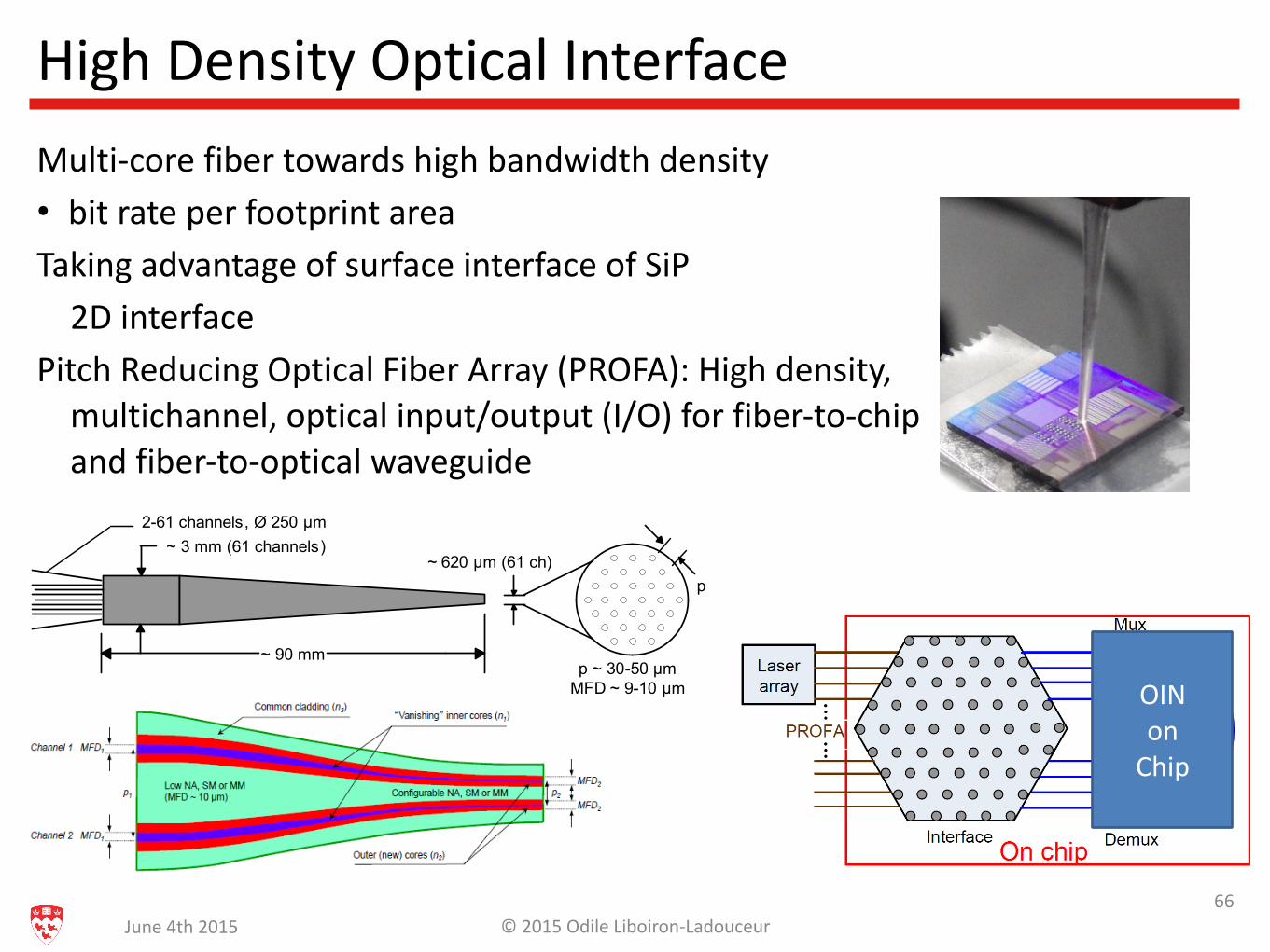
© 2015 Odile Liboiron-‐Ladouceur
High Density Optical InterfaceMulti-‐core fiber towards high bandwidth density • bit rate per footprint area Taking advantage of surface interface of SiP 2D interface Pitch Reducing Optical Fiber Array (PROFA): High density, multichannel, optical input/output (I/O) for fiber-‐to-‐chip and fiber-‐to-‐optical waveguide
66June 4th 2015
~ 90 mm
~ 3 mm (61 channels)~ 620 µm (61 ch)
2-61 channels, Ø 250 µm
p ~ 30-50 µmMFD ~ 9-10 µm
p
OIN on Chip

© 2015 Odile Liboiron-‐Ladouceur
Design and fabrication towards 61 VGCHorizontal and vertical pitch of 42.33 µm and 37.7 µm
67April 15th 2015
Length
Width
Incident angle [deg] Period [μm] Grating tooth [μm] Etch depth [nm]
20 0.66 0.33 70
0.2 mm2 (500 μm × 400 μm) die (IMEC)
θ
β
Polished PROFA
Pitch
z
y
Polishingaxis
nSi = 3.48
nAir = 1
φ
nSiO2 = 1.47x
1520 1530 1540 1550 1560 1570 1580
-20
-18
-16
-14
-12
-10
Wavelength [nm]
Fibe
r to
fiber
loss
[dB
]
VGC(3,4)VGC(8,9)VGC(16,17)VGC(20,21)VGC(33,34)VGC(37,38)VGC(45,46)VGC(48,49)VGC(58,60)
Insertion loss [dB]
3-‐dB bandwidth [nm] Loss difference [dB] Crosstalk [dB]
4.5 50 0.7 -‐50
Peicheng Liao; Sakib, M.; Fei Lou; Jongchul Park; Wlodawski, M.; Kopp, V.I.; Neugroschl, D.; Liboiron-‐Ladouceur, O., "Ultradense Silicon Photonic Interface for Optical Interconnection," Photonics Technology Letters, IEEE , vol.27, no.7, pp.725,728, April1, 1 2015
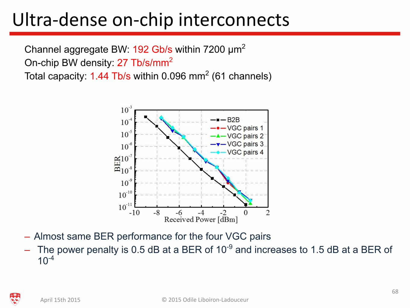
© 2015 Odile Liboiron-‐Ladouceur
Ultra-‐dense on-‐chip interconnectsChannel aggregate BW: 192 Gb/s within 7200 µm2 On-chip BW density: 27 Tb/s/mm2 Total capacity: 1.44 Tb/s within 0.096 mm2 (61 channels)
– Almost same BER performance for the four VGC pairs – The power penalty is 0.5 dB at a BER of 10-9 and increases to 1.5 dB at a BER of
10-4
68April 15th 2015
© 2015 L. ChrostowskiSi-EPIC CREATE
Conclusions
• Leverage• Over 3 decades of CMOS EDA tools + over 2 decades of optical design software
development• Full-flow design environments are becoming a reality for silicon photonics
• Mature CMOS fabrication processes, MPW fabrication runs, Stable processes that are repeatable• enable the development of component libraries for system design • emphasize parameterized components to be more useful for system design
• Evolution towards• Specialized roles as in the electronics industry
• Processing experts• EDA tools• Component / Library / PDK developers• System designers
• Accelerated product development & increasing size of photonics industry
69

© 2015 L. ChrostowskiSi-EPIC CREATE
Keep in Touch with SiEPIC
• LinkedIn• Group: SiEPIC - Silicon Electronic Photonic Integrated Circuits
https://www.linkedin.com/grp/home?gid=6560209
• Facebook• Page: Silicon Photonics Design and Fabrication workshops
https://www.facebook.com/siphotonics
• Mailing list• MailChimp: http://eepurl.com/3LkX1
• EBeam fabrication runs• Google group: https://groups.google.com/d/forum/siepic-ebeam
• SiEPIC Web page• www.siepic.ubc.ca
70