output voltage ripple analysis for dcm of buck, boost, and buck-boost … · · 2000-02-24output...
TRANSCRIPT

Output Voltage Ripple Analysis for
DCM of Buck, Boost, and Buck-Boost
Switching Power Supplies
Scott K. Frederick04/21/99
Term Paper Submission
EEL 6246Power Electronics II
University of Central Florida
Dr. Issa BatarsehSpring 1999

Output Voltage Ripple Analysis forDCM of Buck, Boost, and Buck-Boost Switching Power Supplies
Table of Contents
Page Content
2 Table of Contents
3 Introduction
4 Buck Converter Continuous Conduction
8 Buck Converter Discontinuous Conduction
12 Boost Converter Discontinuous Conduction
19 Buck-Boost Discontinuous Conduction
21 Conclusion
22 References
Introduction
Moving from Power Electronics I to Power Electronics II was a giant step into a
mathematical abyss. Subject material is far more difficult to understand, and the related
analytical mathematics is extremely time consuming and prone to errors. Few references exist on
most of this material, and troubleshooting problems encountered while performing mathematical
analysis is consequently very difficult.
Dealing with the discontinuous conduction mode (DCM) of even the most basic types of
switching power supplies was very frustrating. Specifically, the idea behind analyzing the output
voltage ripple of these converters in the DCM mode should result in the continuous conduction
mode result if the proper parameters are set correctly. This paper will spell out the difficulties
encountered with this approach, and give a detailed mathematical explanation of the output
voltage ripple for three types of converters. The finished product will almost read like an
addition to chapter 7 of the text for this class, which was written by the instructor, Dr. Batarseh.
Some knowledge of basic switching power supplies is required.
The beginning of the paper will review the CCM output voltage ripple analysis of the
buck converter, and then move on to the same analysis for the DCM case. Basic assuption of the
CCM mode will be made for the boost and buck-boost converters. The DCM analysis will be
given in detail. All results will be compared to the CCM mode, and some hints will be given to
aid in comparing CCM mode to DCM mode in these and other similar converters that could save
vast amounts of time to someone performing voltage or current analysis on like converters.
While these derivations are presented in texts as straightforward, about 3 hours of class
time, two hours with a teaching assistant, many hours before paper and many many hours during
the paper writing were spent attempting to derive DCM equations for output ripple voltage. The
concept is straightforward, but the derivations are non-trivial.
All of the analysis in this paper utilize the constant output current model and constant
output voltage model. Clearly, this is a first-order approximation to the system, since the output
voltage is equal to the capacitor voltage, yet we are deriving an expression for the change in
capacitor voltage. There are no component losses included in the analysis either. The main point
of the paper is to reconcile the DCM output voltage ripple with the CCM output voltage ripple.
Generally, DT will be the fraction of a period where the switch in the circuit is closed,
and T-DT will be the fraction of a period where the switch in the circuit is open. D1T-DT will be
the fraction of a period where the inductor current is not zero when the switch is open.
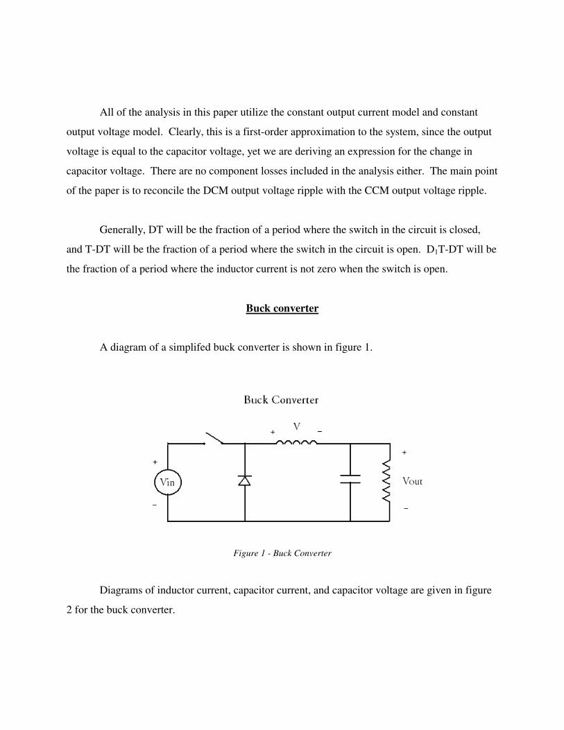
Buck converter
A diagram of a simplifed buck converter is shown in figure 1.
Figure 1 - Buck Converter
Diagrams of inductor current, capacitor current, and capacitor voltage are given in figure
2 for the buck converter.
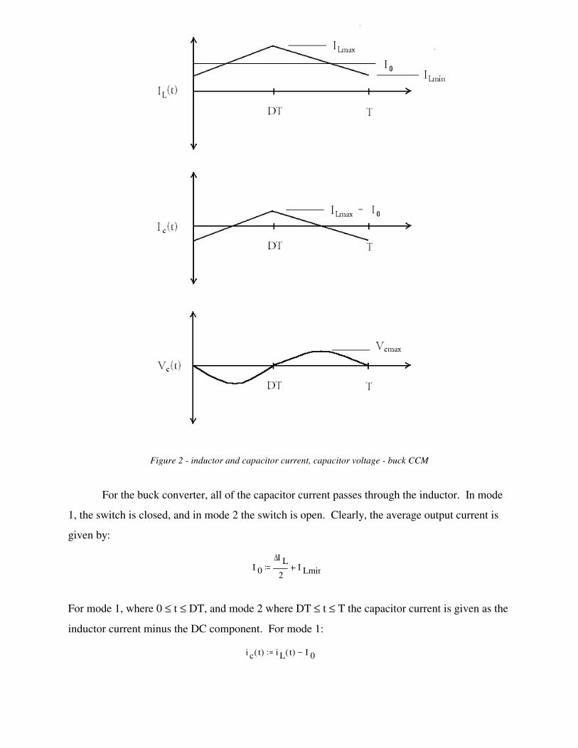
Figure 2 - inductor and capacitor current, capacitor voltage - buck CCM
For the buck converter, all of the capacitor current passes through the inductor. In mode
1, the switch is closed, and in mode 2 the switch is open. Clearly, the average output current is
given by:
For mode 1, where 0 ≤ t ≤ DT, and mode 2 where DT ≤ t ≤ T the capacitor current is given as the
inductor current minus the DC component. For mode 1:
I 0
∆I L
2I Lmin
i c t( ) i L t( ) I 0
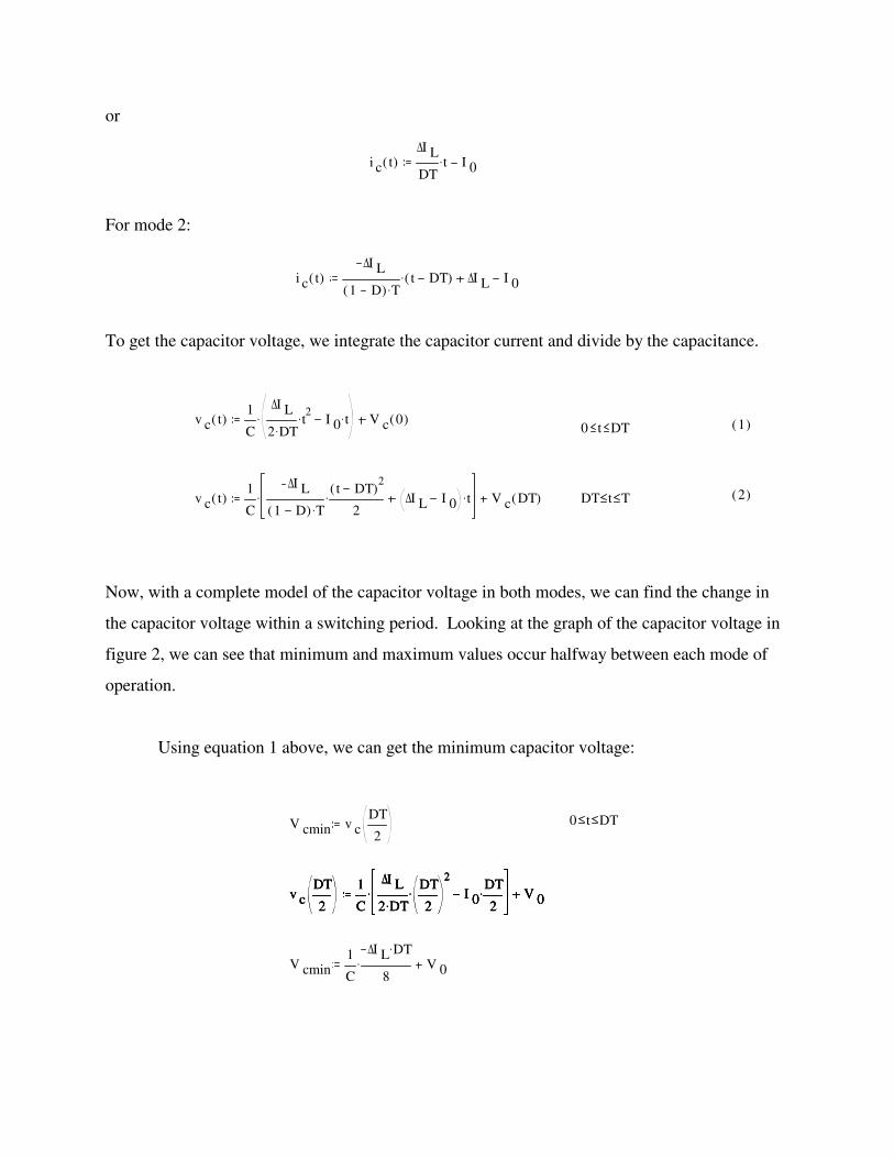
or
For mode 2:
To get the capacitor voltage, we integrate the capacitor current and divide by the capacitance.
Now, with a complete model of the capacitor voltage in both modes, we can find the change in
the capacitor voltage within a switching period. Looking at the graph of the capacitor voltage in
figure 2, we can see that minimum and maximum values occur halfway between each mode of
operation.
Using equation 1 above, we can get the minimum capacitor voltage:
i c t( )∆I L
DTt. I 0
i c t( )∆I L
1 D( ) T.t DT( ). ∆I L I 0
v c t( )1
C
∆I L
2 DT. t2. I 0 t.. V c 0( )
0 t DT
v c t( )1
C
∆I L
1 D( ) T.t DT( )
2
2. ∆I L I 0 t.. V c DT( ) DT t T
1( )
2( )
V cmin v cDT
2
v cDT
2
1
C
∆I L
2 DT.DT
2
2. I 0
DT
2.. V 0v c
DT
2
1
C
∆I L
2 DT.DT
2
2. I 0
DT
2.. V 0v c
DT
2
1
C
∆I L
2 DT.DT
2
2. I 0
DT
2.. V 0
V cmin1
C
∆I L DT.
8. V 0
0 t DT
Likewise, the maximum capacitor voltage is obtained from equation 2 above:
To find the capacitor voltage ripple (also the output voltage ripple), we need a representation for
the inductor current in terms of input voltage. The output voltage terms (DC) will cancel when
the minimum capacitor voltage is subtracted from the maximum capacitor voltage. Knowing that
the inductor voltage is,
and the output voltage can be written as
For a buck converter in CCM, the following integral for the inductor current can be evaluated:
Evaluating the integral at DT to get the maximum inductor current, and at 0 to get the minimum
inductor current, we have:
Subtracting the minimum inductor current from the maximum inductor current, the maximum
V cmax v cT 1 D( ).
2DT t T
V cT 1 D( ).
2
1
C
∆I L
1 D( ) T.
T 1 D( ).
2DT
2
2. ∆I L I 0
T 1 D( ).
2.. V 0
V cmax1
C
∆I L T. 1 D( ).
8. V 0
v L V in V outV outV out
V out D V in.V inV in
i L t( )1
L0
DT
tv L t( ) d. I L 0( )I LI L
i Lmax
V in
L1 D( ). DT. I L 0( )I LI L
i Lmin I L 0( )I LI L
change in the inductor current can be found:
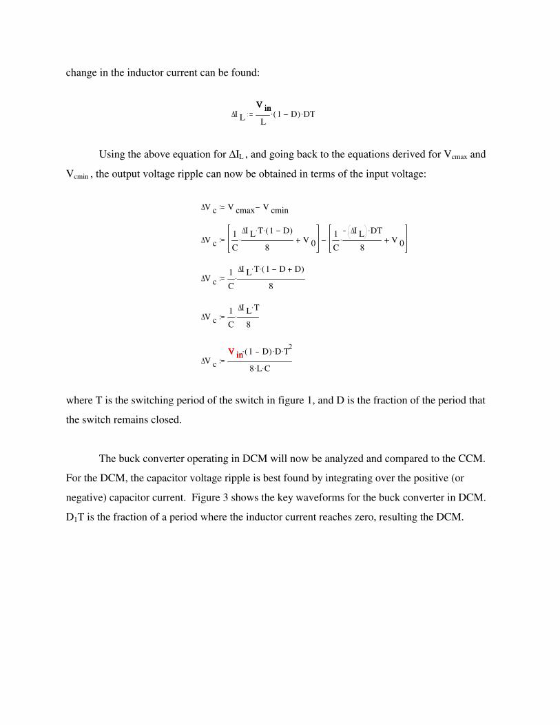
Using the above equation for ∆IL , and going back to the equations derived for Vcmax and
Vcmin , the output voltage ripple can now be obtained in terms of the input voltage:
where T is the switching period of the switch in figure 1, and D is the fraction of the period that
the switch remains closed.
The buck converter operating in DCM will now be analyzed and compared to the CCM.
For the DCM, the capacitor voltage ripple is best found by integrating over the positive (or
negative) capacitor current. Figure 3 shows the key waveforms for the buck converter in DCM.
D1T is the fraction of a period where the inductor current reaches zero, resulting the DCM.
∆I L
V in
L1 D( ). DT.
V inV in
∆V c V cmax V cmin
∆V c1
C
∆I L T. 1 D( ).
8. V 0
1
C
∆I L DT.
8. V 0
∆V c1
C
∆I L T. 1 D D( ).
8.
∆V c1
C
∆I L T.
8.
∆V c
V in 1 D( ). D. T2.
8 L. C.
V inV in
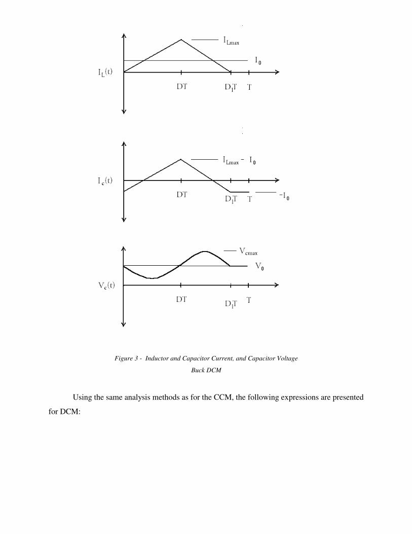
Figure 3 - Inductor and Capacitor Current, and Capacitor Voltage
Buck DCM
Using the same analysis methods as for the CCM, the following expressions are presented
for DCM:
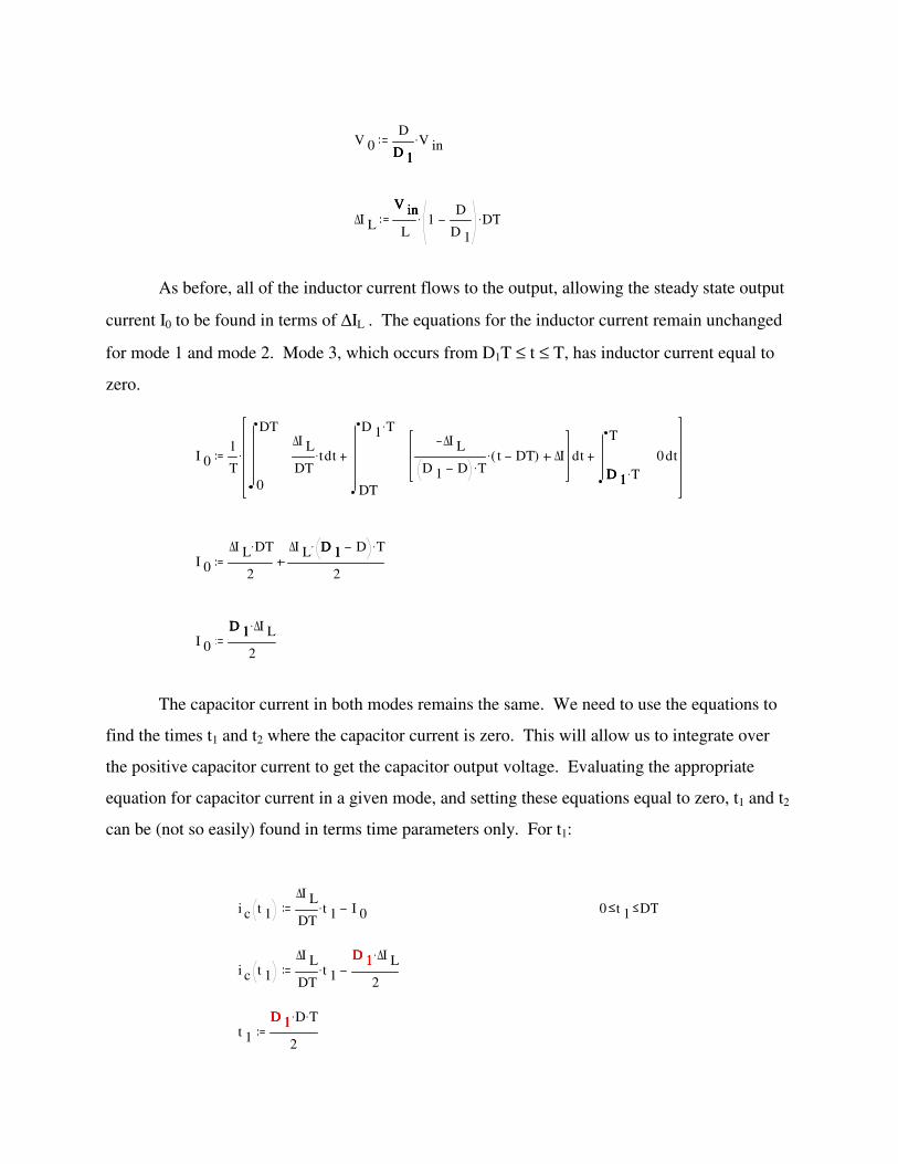
As before, all of the inductor current flows to the output, allowing the steady state output
current I0 to be found in terms of ∆IL . The equations for the inductor current remain unchanged
for mode 1 and mode 2. Mode 3, which occurs from D1T ≤ t ≤ T, has inductor current equal to
zero.
The capacitor current in both modes remains the same. We need to use the equations to
find the times t1 and t2 where the capacitor current is zero. This will allow us to integrate over
the positive capacitor current to get the capacitor output voltage. Evaluating the appropriate
equation for capacitor current in a given mode, and setting these equations equal to zero, t1 and t2
can be (not so easily) found in terms time parameters only. For t1:
V 0D
D 1V in
.D 1D 1
∆I L
V in
L1
D
D 1
. DT.V inV in
I 01
T0
DT
t∆I L
DTt. d
DT
D 1 T.
t∆I L
D 1 D T.t DT( ). ∆I d
D 1 T.
T
t0d.D 1D 1
I 0
∆I L DT.
2
∆I L D 1 D. T.
2
D 1D 1
I 0
D 1 ∆I L.
2
D 1D 1
i c t 1
∆I L
DTt 1
. I 0 0 t 1 DT
i c t 1
∆I L
DTt 1
.D 1 ∆I L
.
2
D 1D 1
t 1
D 1 D. T.
2
D 1D 1

And for t2:
The capacitor voltage is given by:
Ignoring the initial voltage, a DC component, the above integral yields ∆VC .
Substituting for t1 , t2 , I0 , and ∆IL , the output voltage ripple can be obtained in terms of Vin.
i c t 2
∆I L
D 1 D T.t 2 DT. ∆I L I 0D 1D 1
DT t 2 T
i c t 2
∆I L
D 1 D T.t 2 DT. ∆I L
D 1 ∆I L.
2
∆I L
t 2 1D 1
2D 1 D. T. DT
D 1D 1
t 2 D 1
D 12
2D
D 1 D.
2D T.
D 1D 1
t 2 D 1
D 12
2
D 1 D.
2T.
D 1D 1
v c t( )1
Ct 1
t 2
ti c t( ) d. V c t 1
∆V c1
C
1
2. t 2 t 1
. ∆I L I 0.t 1t 1
∆V c1
2 C.D 1
D 12
2
D 1 D.
2T.
D 1 D. T.
2.
V in
L1
D
D 1
. DT.D 1 ∆I L
.
2.
D 1D 1
∆V c1
2 C.D 1
D 12
2T..
V in
L1
D
D 1
. DT. 1D 1
2..
D 1D 1
∆V c
V in D. T2.
2 L. C.D 1
D 12
2. 1
D
D 1
. 1D 1
2.
V inV in
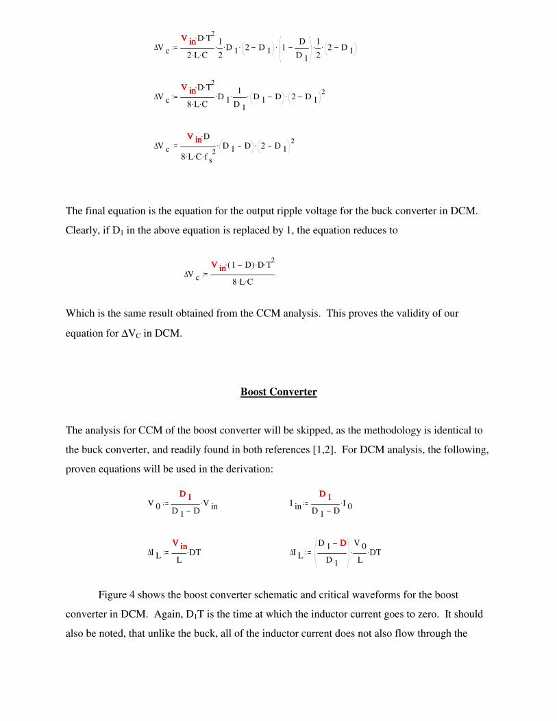
The final equation is the equation for the output ripple voltage for the buck converter in DCM.
Clearly, if D1 in the above equation is replaced by 1, the equation reduces to
Which is the same result obtained from the CCM analysis. This proves the validity of our
equation for ∆VC in DCM.
Boost Converter
The analysis for CCM of the boost converter will be skipped, as the methodology is identical to
the buck converter, and readily found in both references [1,2]. For DCM analysis, the following,
proven equations will be used in the derivation:
Figure 4 shows the boost converter schematic and critical waveforms for the boost
converter in DCM. Again, D1T is the time at which the inductor current goes to zero. It should
also be noted, that unlike the buck, all of the inductor current does not also flow through the
∆V c
V in D. T2.
2 L. C.1
2. D 1
. 2 D 1. 1
D
D 1
. 1
2. 2 D 1
.V inV in
∆V c
V in D. T2.
8 L. C.D 1
. 1
D 1
. D 1 D. 2 D 12.
V inV in
∆V c
V in D.
8 L. C. f s2.
D 1 D. 2 D 12.
V inV in
∆V c
V in 1 D( ). D. T2.
8 L. C.
V inV in
V 0
D 1
D 1 DV in
.D 1D 1
I in
D 1
D 1 DI 0
.D 1D 1
∆I L
V in
LDT.
V inV in∆I L
D 1 D
D 1
V 0
L. DT.
DD

Figure 4 - Boost schematic and relevant waveforms for boost DCM
output.
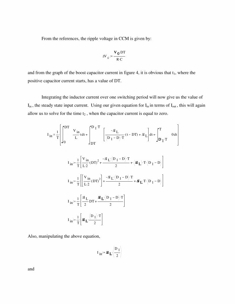
From the references, the ripple voltage in CCM is given by:
and from the graph of the boost capacitor current in figure 4, it is obvious that t1, where the
positive capacitor current starts, has a value of DT.
Integrating the inductor current over one switching period will now give us the value of
Iin , the steady state input current. Using our given equation for Iin in terms of Iout , this will again
allow us to solve for the time t2 , when the capacitor current is equal to zero.
Also, manipulating the above equation,
and
∆V c
V 0 DT.
R C.
V 0V 0
I in1
T0
DT
tV in
Lt. d
DT
D 1 T.
t∆I L
D 1 D T.t DT( ). ∆I L d
D 1 T.
T
t0d.D 1D 1
I in1
T
V in
L 2.DT( )
2.∆I L D 1 D. T.
2∆I L T. D 1 D.. ∆I L∆I L
I in1
T
V in
L 2.DT( )
2.∆I L D 1 D. T.
2∆I L T. D 1 D.. ∆I L∆I L
I in1
T
∆I L
2DT.
∆I L D 1 D. T.
2.
∆I L∆I L
I in1
T∆I L
D 1 T.
2.. ∆I L∆I L
I in ∆I L
D 1
2.∆I L∆I L
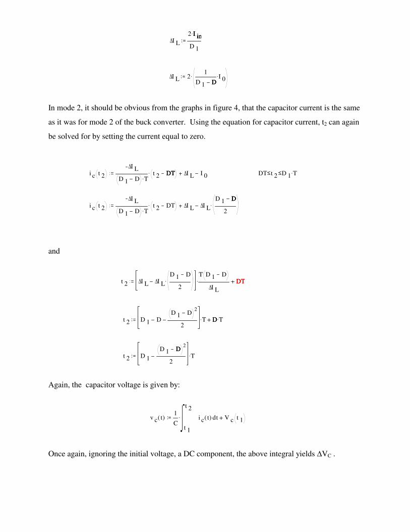
In mode 2, it should be obvious from the graphs in figure 4, that the capacitor current is the same
as it was for mode 2 of the buck converter. Using the equation for capacitor current, t2 can again
be solved for by setting the current equal to zero.
and
Again, the capacitor voltage is given by:
Once again, ignoring the initial voltage, a DC component, the above integral yields ∆VC .
∆I L
2 I in.
D 1
I inI in
∆I L 21
D 1 DI 0
..DD
i c t 2
∆I L
D 1 D T.t 2 DT. ∆I L I 0DTDT DT t 2 D 1 T.
i c t 2
∆I L
D 1 D T.t 2 DT. ∆I L ∆I L
D 1 D
2.
DD
t 2 ∆I L ∆I L
D 1 D
2.
T D 1 D
∆I L
. DTDTDT
t 2 D 1 DD 1 D
2
2T. D T.DD
t 2 D 1
D 1 D2
2T.
DD
v c t( )1
Ct 1
t 2
ti c t( ) d. V c t 1
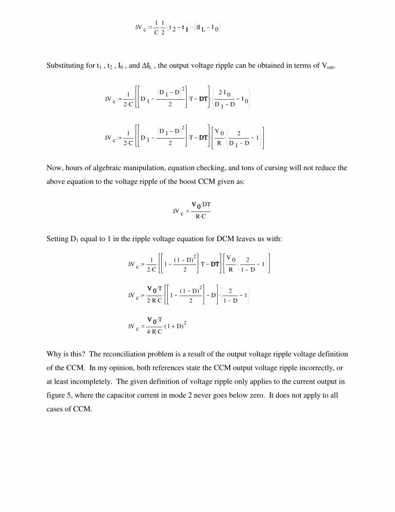
Substituting for t1 , t2 , I0 , and ∆IL , the output voltage ripple can be obtained in terms of Vout.
Now, hours of algebraic manipulation, equation checking, and tons of cursing will not reduce the
above equation to the voltage ripple of the boost CCM given as:
Setting D1 equal to 1 in the ripple voltage equation for DCM leaves us with:
Why is this? The reconciliation problem is a result of the output voltage ripple voltage definition
of the CCM. In my opinion, both references state the CCM output voltage ripple incorrectly, or
at least incompletely. The given definition of voltage ripple only applies to the current output in
figure 5, where the capacitor current in mode 2 never goes below zero. It does not apply to all
cases of CCM.
∆V c1
C
1
2. t 2 t 1
. ∆I L I 0.t 1t 1
∆V c1
2 C.D 1
D 1 D2
2T. DT.
2 I 0.
D 1 DI 0
.DTDT
∆V c1
2 C.D 1
D 1 D2
2T. DT.
V 0
R
2
D 1 D1..DTDT
∆V c
V 0 DT.
R C.
V 0V 0
∆V c1
2 C.1
1 D( )2
2T. DT.
V 0
R
2
1 D1..DTDT
∆V c
V 0 T.
2 R. C.1
1 D( )2
2D. 2
1 D1.
V 0V 0
∆V c
V 0 T.
4 R. C.1 D( )
2.V 0V 0
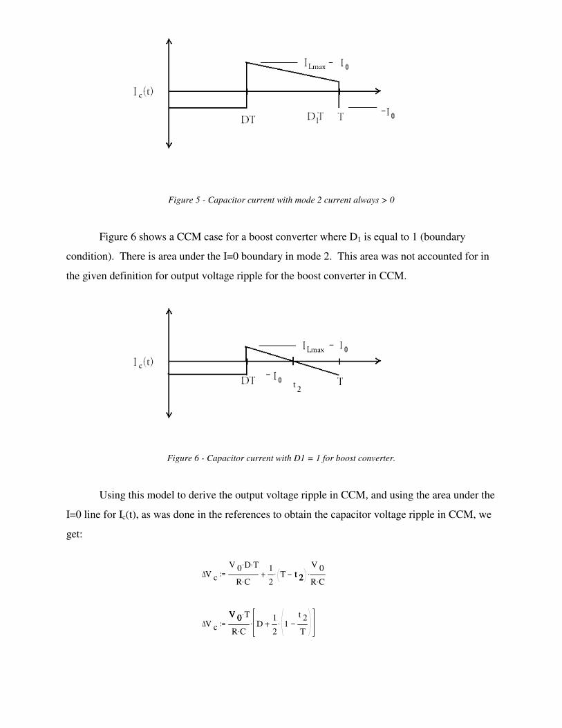
Figure 5 - Capacitor current with mode 2 current always > 0
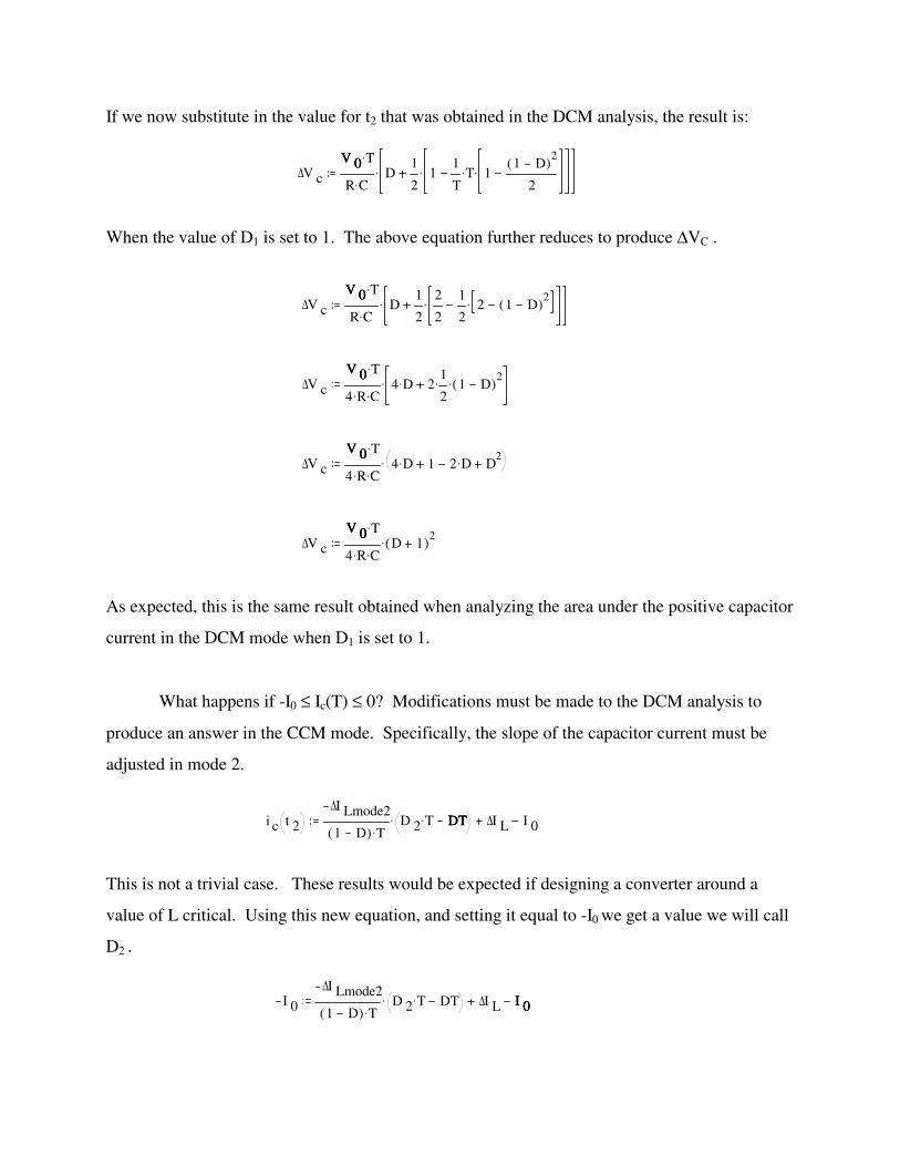
Figure 6 shows a CCM case for a boost converter where D1 is equal to 1 (boundary
condition). There is area under the I=0 boundary in mode 2. This area was not accounted for in
the given definition for output voltage ripple for the boost converter in CCM.
Figure 6 - Capacitor current with D1 = 1 for boost converter.
Using this model to derive the output voltage ripple in CCM, and using the area under the
I=0 line for Ic(t), as was done in the references to obtain the capacitor voltage ripple in CCM, we
get:
∆V c
V 0 D. T.
R C.1
2T t 2
.V 0
R C..t 2t 2
∆V c
V 0 T.
R C.D
1
21
t 2
T..
V 0V 0
If we now substitute in the value for t2 that was obtained in the DCM analysis, the result is:
When the value of D1 is set to 1. The above equation further reduces to produce ∆VC .
As expected, this is the same result obtained when analyzing the area under the positive capacitor
current in the DCM mode when D1 is set to 1.
What happens if -I0 ≤ Ic(T) ≤ 0? Modifications must be made to the DCM analysis to
produce an answer in the CCM mode. Specifically, the slope of the capacitor current must be
adjusted in mode 2.
This is not a trivial case. These results would be expected if designing a converter around a
value of L critical. Using this new equation, and setting it equal to -I0 we get a value we will call
D2 .
∆V c
V 0 T.
R C.D
1
21
1
TT. 1
1 D( )2
2...
V 0V 0
∆V c
V 0 T.
R C.D
1
2
2
2
1
22 1 D( )
2...V 0V 0
∆V c
V 0 T.
4 R. C.4 D. 2
1
2. 1 D( )
2..V 0V 0
∆V c
V 0 T.
4 R. C.4 D. 1 2 D. D
2.V 0V 0
∆V c
V 0 T.
4 R. C.D 1( )
2.V 0V 0
i c t 2
∆I Lmode2
1 D( ) T.D 2 T. DT. ∆I L I 0DTDT
I 0
∆I Lmode2
1 D( ) T.D 2 T. DT. ∆I L I 0I 0I 0
The change in inductor current in mode 2 can be obtained from the inductor current
equation for mode 2, remembering that VL = Vin - V0 for a first order analysis. Solving for D2 ,
we obtain:
where D2 is larger than T, and can now be used to find t2 by using the DCM equation for t2 and
substituting D2 for D1 without further changes. It follows that t2 can now be used to evaluate the
following integral to obtain the capacitor voltage ripple.
It is important to evaluate the initial capacitor voltage at time DT using CCM analysis,
but use the equation for ic(t) in the DCM analysis changing, D1 to D2 . However, the initial
capacitor voltage, a DC value, is not required if the desired result is only the output ripple
voltage. The CCM output ripple voltage is not exactly straightforward, but it will produce a
good first order solution for the output (capacitor) voltage ripple for this case.
Buck-Boost Converter
Well, if you ever needed some luck, it can be found with the buck-boost analysis. The buck
boost converter is shown in figure 7.
D 2 T. 1 D( ) T.∆I L
∆I Lmode2
. D T.DD
D 2 1 D( )∆I L
∆I Lmode2
. DDD
v c t( )1
CDT
t 2
ti c t( ) d. V c DT( )DTDT

Figure 7 - Buck-Boost Converter.
The relevant waveforms are identical to those in figure 4.
Mode 2 inductor current is just like the boost converter. Mode 1 and mode 3 capacitor
current in DCM are simply -I0 . The analysis produces the same output capacitor voltage ripple
as found in the boost converter.
Conclusion
This paper has presented a step-by-step first order analysis of the buck and boost
converter output ripple voltage in DCM. The buck-boost converter output ripple voltage is
exactly like the boost output ripple voltage in DCM. The equations for the output ripple voltage
in DCM were shown to reduce to the output ripple voltage equations in CCM. Important notes
were given on the boost converter capacitor current to show what must be done for the equations
to reconcile properly.
The texts advertise the process as straightforward, and indeed the concept is quite basic.
From an educational standpoint however, it is not straightforward to ask a student to reduce the
DCM output ripple voltage to the given
as it is not possible when setting D1 = 1 in the equation for DCM. How many hours does a
student spend working before the student realizes the problems with the given equation pointed
out in this paper? 5, 10, 20, 40, or more? You would question the integrity of those claiming to
have proved the output ripple voltage in DCM does reduce to the above equation. IT DOES
NOT. The information in this paper should be given up front so the obvious fact, that integrating
the positive capacitor current results in the output ripple voltage for any mode of operation, can
be realized and the student can move on to more difficult conceptual topics.
It should also be noted that it is rather challenging to get the equations for t1 , t2 , I0 , and
∆IL in terms of Vin or Vout correct. Special attention to these parameters is required to avoid
unnecessary mistakes when deriving output ripple voltage. The graphs of the inductor and
capacitor current are useful, but do not tell the whole story. The proper assumptions about the
gain and order of the model must be made and remain consistent throughout the analysis.
Finally, an equation was given and all the parameters defined to obtain the output
∆V c
V 0 DT.
R C.
V 0V 0

capacitor ripple voltage for the boost and buck-boost converter in CCM for all cases. This
equation is actually more difficult to obtain than the DCM counterpart. This paper is a must read
for any student studying the basic converters in power electronics for the first time, at any level.
It does indeed help the supposedly straight forward become realizable if the student is inclined to
work out all of the details of the output ripple voltage for basic converters, as students should.
References
[1] Mohan, N., Undeland, T. M., Robbins, W. P., Power Electronics: Converters,
Applications, and Design, Second Edition, John Wiley and Sons, Inc., New York, NY,
1995.
[2] Batarseh, Issa, Power Electronic Circuits, University of Central Florida (not yet in print)