isl95338 fn8896 bidirectional buck-boost voltage regulator … · 2017-10-08 · bidirectional...
TRANSCRIPT
FN8896 Rev.1.00 Page 1 of 48Oct 5, 2017
FN8896Rev.1.00
Oct 5, 2017
ISL95338Bidirectional Buck-Boost Voltage Regulator
DATASHEET
The ISL95338 is a bidirectional, buck-boost voltage regulator that provides buck-boost voltage regulation and protection features. Intersil’s advanced R3™ Technology is used to provide high light-load efficiency, fast transient response, and seamless DCM/CCM transitions.
The ISL95338 takes input power from a wide range of DC power sources (conventional AC/DC ADPs, USB PD ports, travel ADPs, etc.) and safely converts it to a regulated voltage up to 24V. The ISL95338 can also convert a wide range DC power source connected at its output (system side) to a regulated voltage to its input (ADP side). This bidirectional buck-boost regulation feature makes its application very flexible.
The ISL95338 includes various system operation functions such as Forward mode enable, Reverse mode enable, programmable soft-start time, and adjustable VOUT in both the forward direction and reverse direction. The protection functionalities include OCP, OVP, UVP, OTP, etc.
The ISL95338 has serial communication through SMBus/I2C that allows programming of many critical parameters to deliver a customized solution. These programming parameters include, but are not limited to: output current limit, input current limit, and output voltage setting.
Related Literature• For a full list of related documents, visit our website
• ISL95338 product page
Features• Bidirectional buck, boost, and buck-boost operation
• Input voltage range 3.8V to 24V (no dead zone)
• Output voltage up to 20V
• Up to 1MHz switching frequency
• Programmable soft-start time
• LDO output for VDD and VDDP
• System status alert function
• Bidirectional internal discharge function
• Active switching for negative voltage transitions
• Bypass mode in both directions
• Forward mode enable, Reverse mode enable
• OCP, OVP, UVP, and OTP protection
• SMBus and auto-increment I2C compatible
• Pb-free (RoHS compliant)
• 32 Ld 4x4 TQFN Package
Applications• Tablet, ultrabook, power bank, mobile devices, and
USB-C
FN8896 Rev.1.00 Page 2 of 48Oct 5, 2017
ISL95338
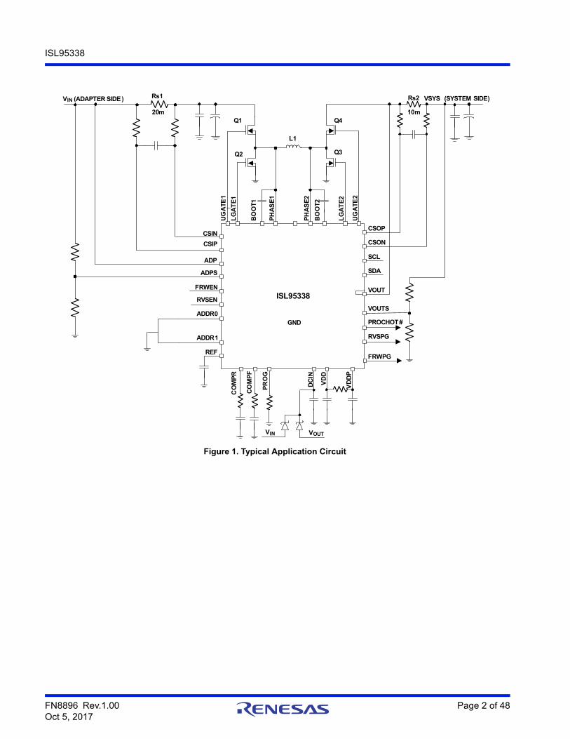
Figure 1. Typical Application Circuit
ISL95338
BO
OT
1
PH
AS
E1
UG
AT
E1
VD
DP
LG
AT
E1
LG
AT
E2
UG
AT
E2
PH
AS
E2
BO
OT
2
SCL
SDA
CSOP
CSON
DC
IN
VD
D
CO
MP
F
FRWPG
RVSEN
ADPS
FRWEN
GND
CSIP
CSIN
ADDR0
VIN (ADAPTER SIDE) VSYS (SYSTEM SIDE)
PR
OG
20m
VIN VOUT
PROCHOT#
ADP
Q1
Q2
Q4
Q3
Rs1
L1
10m
Rs2
VOUTS
VOUT
RVSPG
CO
MP
R
ADDR1
REF

FN8896 Rev.1.00 Page 3 of 48Oct 5, 2017
ISL95338
Contents
1. Overview. . . . . . . . . . . . . . . . . . . . . . . . . . . . . . . . . . . . . . . . . . . . . . . . . . . . . . . . . . . . . . . . . . . . . 5
1.1 Block Diagram . . . . . . . . . . . . . . . . . . . . . . . . . . . . . . . . . . . . . . . . . . . . . . . . . . . . . . . . . . . . . . 5
1.2 Simplified Application Circuit . . . . . . . . . . . . . . . . . . . . . . . . . . . . . . . . . . . . . . . . . . . . . . . . . . . 6
1.3 Ordering Information . . . . . . . . . . . . . . . . . . . . . . . . . . . . . . . . . . . . . . . . . . . . . . . . . . . . . . . . . 6
1.4 Pin Configuration . . . . . . . . . . . . . . . . . . . . . . . . . . . . . . . . . . . . . . . . . . . . . . . . . . . . . . . . . . . . 7
1.5 Pin Descriptions. . . . . . . . . . . . . . . . . . . . . . . . . . . . . . . . . . . . . . . . . . . . . . . . . . . . . . . . . . . . . 7
2. Specifications. . . . . . . . . . . . . . . . . . . . . . . . . . . . . . . . . . . . . . . . . . . . . . . . . . . . . . . . . . . . . . . . . 9
2.1 Absolute Maximum Ratings . . . . . . . . . . . . . . . . . . . . . . . . . . . . . . . . . . . . . . . . . . . . . . . . . . . . 9
2.2 Thermal Information. . . . . . . . . . . . . . . . . . . . . . . . . . . . . . . . . . . . . . . . . . . . . . . . . . . . . . . . . 10
2.3 Recommended Operation Conditions . . . . . . . . . . . . . . . . . . . . . . . . . . . . . . . . . . . . . . . . . . . 10
2.4 Electrical Specifications . . . . . . . . . . . . . . . . . . . . . . . . . . . . . . . . . . . . . . . . . . . . . . . . . . . . . . 10
2.5 SMBus Timing Specification . . . . . . . . . . . . . . . . . . . . . . . . . . . . . . . . . . . . . . . . . . . . . . . . . . 14
3. Typical Performance Curves. . . . . . . . . . . . . . . . . . . . . . . . . . . . . . . . . . . . . . . . . . . . . . . . . . . . 15
4. General SMBus Architecture . . . . . . . . . . . . . . . . . . . . . . . . . . . . . . . . . . . . . . . . . . . . . . . . . . . 18
4.1 Data Validity . . . . . . . . . . . . . . . . . . . . . . . . . . . . . . . . . . . . . . . . . . . . . . . . . . . . . . . . . . . . . . . 18
4.2 START and STOP Conditions . . . . . . . . . . . . . . . . . . . . . . . . . . . . . . . . . . . . . . . . . . . . . . . . . 18
4.3 Acknowledge . . . . . . . . . . . . . . . . . . . . . . . . . . . . . . . . . . . . . . . . . . . . . . . . . . . . . . . . . . . . . . 19
4.4 SMBus Transactions . . . . . . . . . . . . . . . . . . . . . . . . . . . . . . . . . . . . . . . . . . . . . . . . . . . . . . . . 19
4.5 Byte Format . . . . . . . . . . . . . . . . . . . . . . . . . . . . . . . . . . . . . . . . . . . . . . . . . . . . . . . . . . . . . . . 19
4.6 SMBus and I2C Compatibility . . . . . . . . . . . . . . . . . . . . . . . . . . . . . . . . . . . . . . . . . . . . . . . . . 19
5. ISL95338 SMBus Commands . . . . . . . . . . . . . . . . . . . . . . . . . . . . . . . . . . . . . . . . . . . . . . . . . . . 20
5.1 Setting System Side Current Limit. . . . . . . . . . . . . . . . . . . . . . . . . . . . . . . . . . . . . . . . . . . . . . 21
5.2 Setting Input Current Limit in Forward Mode . . . . . . . . . . . . . . . . . . . . . . . . . . . . . . . . . . . . . . 22
5.3 Setting System Regulating Voltage in Forward Mode . . . . . . . . . . . . . . . . . . . . . . . . . . . . . . . 24
5.4 Setting PROCHOT# Threshold for ADP Side Overcurrent Condition . . . . . . . . . . . . . . . . . . . 25
5.5 Setting PROCHOT# Threshold for System Side Overcurrent Condition . . . . . . . . . . . . . . . . . 25
5.6 Setting PROCHOT# Debounce Time and Duration Time . . . . . . . . . . . . . . . . . . . . . . . . . . . . 26
5.7 Control Registers . . . . . . . . . . . . . . . . . . . . . . . . . . . . . . . . . . . . . . . . . . . . . . . . . . . . . . . . . . . 26
5.8 Regulating Voltage Register in Reverse Mode . . . . . . . . . . . . . . . . . . . . . . . . . . . . . . . . . . . . 31
5.9 Output Current Limit Register in Reverse Mode . . . . . . . . . . . . . . . . . . . . . . . . . . . . . . . . . . . 32
5.10 Input Voltage Limit Register. . . . . . . . . . . . . . . . . . . . . . . . . . . . . . . . . . . . . . . . . . . . . . . . . . . 32
5.11 Information Register . . . . . . . . . . . . . . . . . . . . . . . . . . . . . . . . . . . . . . . . . . . . . . . . . . . . . . . . 33
6. Application Information. . . . . . . . . . . . . . . . . . . . . . . . . . . . . . . . . . . . . . . . . . . . . . . . . . . . . . . . 34
6.1 R3 Modulator . . . . . . . . . . . . . . . . . . . . . . . . . . . . . . . . . . . . . . . . . . . . . . . . . . . . . . . . . . . . . . 34
6.2 ISL95338 Bidirectional Buck-Boost Voltage Regulator . . . . . . . . . . . . . . . . . . . . . . . . . . . . . . 36
6.3 Soft-Start . . . . . . . . . . . . . . . . . . . . . . . . . . . . . . . . . . . . . . . . . . . . . . . . . . . . . . . . . . . . . . . . . 37
6.4 Programming Options . . . . . . . . . . . . . . . . . . . . . . . . . . . . . . . . . . . . . . . . . . . . . . . . . . . . . . . 37
6.5 DE Operation . . . . . . . . . . . . . . . . . . . . . . . . . . . . . . . . . . . . . . . . . . . . . . . . . . . . . . . . . . . . . . 38
FN8896 Rev.1.00 Page 4 of 48Oct 5, 2017
ISL95338
6.6 Forward Mode . . . . . . . . . . . . . . . . . . . . . . . . . . . . . . . . . . . . . . . . . . . . . . . . . . . . . . . . . . . . . 39
6.7 Reverse Mode for USB OTG (On-the-Go). . . . . . . . . . . . . . . . . . . . . . . . . . . . . . . . . . . . . . . . 39
6.8 Fast REF . . . . . . . . . . . . . . . . . . . . . . . . . . . . . . . . . . . . . . . . . . . . . . . . . . . . . . . . . . . . . . . . . 39
6.9 Fast Swap . . . . . . . . . . . . . . . . . . . . . . . . . . . . . . . . . . . . . . . . . . . . . . . . . . . . . . . . . . . . . . . . 39
6.10 ADP Input Overvoltage Protection. . . . . . . . . . . . . . . . . . . . . . . . . . . . . . . . . . . . . . . . . . . . . . 40
6.11 System Output Overvoltage Protection . . . . . . . . . . . . . . . . . . . . . . . . . . . . . . . . . . . . . . . . . . 40
6.12 System Output Undervoltage Protection . . . . . . . . . . . . . . . . . . . . . . . . . . . . . . . . . . . . . . . . . 40
6.13 ADP Output Overvoltage Protection . . . . . . . . . . . . . . . . . . . . . . . . . . . . . . . . . . . . . . . . . . . . 40
6.14 ADP Output Undervoltage Protection . . . . . . . . . . . . . . . . . . . . . . . . . . . . . . . . . . . . . . . . . . . 40
6.15 Over-Temperature Protection . . . . . . . . . . . . . . . . . . . . . . . . . . . . . . . . . . . . . . . . . . . . . . . . . 40
6.16 Switching Power MOSFET Gate Capacitance. . . . . . . . . . . . . . . . . . . . . . . . . . . . . . . . . . . . . 40
6.17 ADP Side Input Filter . . . . . . . . . . . . . . . . . . . . . . . . . . . . . . . . . . . . . . . . . . . . . . . . . . . . . . . . 41
7. General Application Information . . . . . . . . . . . . . . . . . . . . . . . . . . . . . . . . . . . . . . . . . . . . . . . . 42
7.1 Select the LC Output Filter . . . . . . . . . . . . . . . . . . . . . . . . . . . . . . . . . . . . . . . . . . . . . . . . . . . 42
7.2 Select the Input Capacitor . . . . . . . . . . . . . . . . . . . . . . . . . . . . . . . . . . . . . . . . . . . . . . . . . . . . 43
7.3 Select the Switching Power MOSFET . . . . . . . . . . . . . . . . . . . . . . . . . . . . . . . . . . . . . . . . . . . 44
7.4 Select the Bootstrap Capacitor . . . . . . . . . . . . . . . . . . . . . . . . . . . . . . . . . . . . . . . . . . . . . . . . 44
7.5 Select the Resistor Divider for VOUTS and ADPS . . . . . . . . . . . . . . . . . . . . . . . . . . . . . . . . . 45
8. Revision History. . . . . . . . . . . . . . . . . . . . . . . . . . . . . . . . . . . . . . . . . . . . . . . . . . . . . . . . . . . . . . 46
9. Package Outline Drawing . . . . . . . . . . . . . . . . . . . . . . . . . . . . . . . . . . . . . . . . . . . . . . . . . . . . . . 47
10. About Intersil . . . . . . . . . . . . . . . . . . . . . . . . . . . . . . . . . . . . . . . . . . . . . . . . . . . . . . . . . . . . . . . . 48
FN8896 Rev.1.00 Page 5 of 48Oct 5, 2017
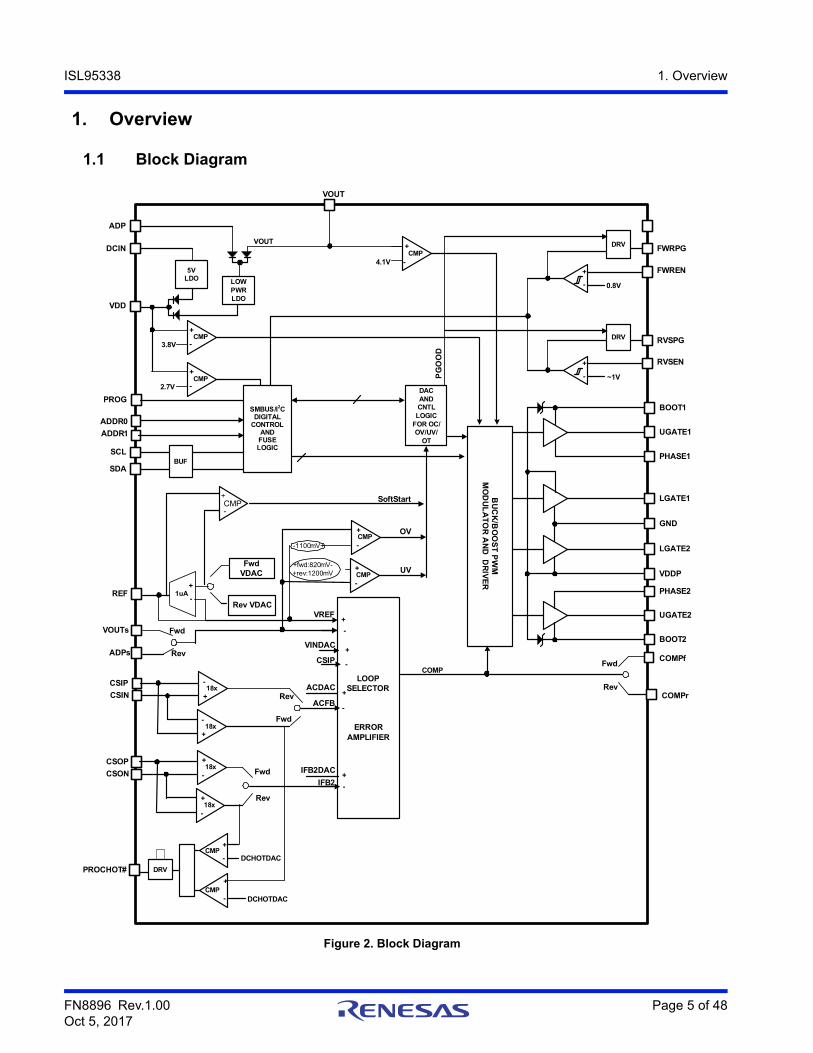
ISL95338 1. Overview
1. Overview
1.1 Block Diagram
Figure 2. Block Diagram
PROG
SCL
SMBUS/I2CDIGITAL
CONTROL AND
FUSELOGIC
DACANDCNTL
LOGIC FOR OC/OV/UV/
OT
5V LDO
BU
CK
/BO
OS
T P
WM
MO
DU
LA
TO
R A
ND
DR
IVE
R
DRV
0.8V
CSIN
CSIP
VDD
SDA
DCIN FWRPG
FWREN
BOOT1
UGATE1
PHASE1
LGATE1
GND
LGATE2
VDDP
PHASE2
UGATE2
BOOT2
COMPr
DRVPROCHOT#
BUF
ADP
VREF
ACDAC
ACFB
IFB2DAC
IFB2
CSIP
VINDAC
LOW PWR LDO
VOUT
CMP
CMP
DCHOTDAC
CMP4.1V
CMP
CMP
3.8V
2.7V
+
-
+
+
-
+
-
-
+
+
-
-
-
-
+
+
+
+-
-
Rev
FwdCSON
CSOP
18x+
-
18x+
-
Rev
Fwd18x
-
+
18x-
+
VOUT
Rev
FwdCOMPf
COMP
DRV
~1V
RVSPG
RVSEN+
-
ADDR1
ADDR0
Fwd VDAC
+
-1uA
Rev VDAC
REF
VOUTs
ADPs
Fwd
Rev
DCHOTDAC
CMP+
-
CMP+
-
OV
UV
-1100mV+
+fwd:820mV-+rev:1200mV
CMP+
-
SoftStart
PG
OO
D
LOOPSELECTOR
ERRORAMPLIFIER
FN8896 Rev.1.00 Page 6 of 48Oct 5, 2017
ISL95338 1. Overview
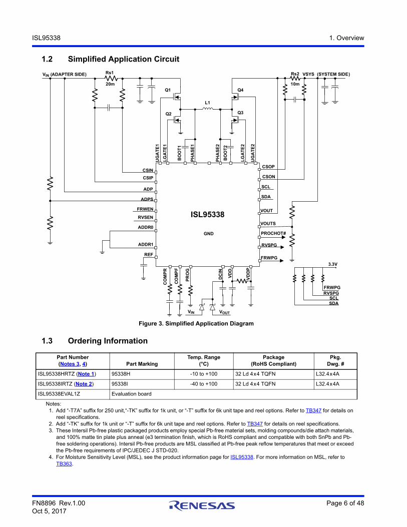
1.2 Simplified Application Circuit
Figure 3. Simplified Application Diagram
1.3 Ordering Information
Part Number(Notes 3, 4) Part Marking
Temp. Range(°C)
Package(RoHS Compliant)
Pkg.Dwg. #
ISL95338HRTZ (Note 1) 95338H -10 to +100 32 Ld 4x4 TQFN L32.4x4A
ISL95338IRTZ (Note 2) 95338I -40 to +100 32 Ld 4x4 TQFN L32.4x4A
ISL95338EVAL1Z Evaluation board
Notes:1. Add “-T7A” suffix for 250 unit,“-TK” suffix for 1k unit, or “-T” suffix for 6k unit tape and reel options. Refer to TB347 for details on
reel specifications.2. Add “-TK” suffix for 1k unit or “-T” suffix for 6k unit tape and reel options. Refer to TB347 for details on reel specifications.3. These Intersil Pb-free plastic packaged products employ special Pb-free material sets, molding compounds/die attach materials,
and 100% matte tin plate plus anneal (e3 termination finish, which is RoHS compliant and compatible with both SnPb and Pb-free soldering operations). Intersil Pb-free products are MSL classified at Pb-free peak reflow temperatures that meet or exceed the Pb-free requirements of IPC/JEDEC J STD-020.
4. For Moisture Sensitivity Level (MSL), see the product information page for ISL95338. For more information on MSL, refer to TB363.
ISL95338
BO
OT
1
PH
AS
E1
UG
AT
E1
VD
DP
LG
AT
E1
LG
AT
E2
UG
AT
E2
PH
AS
E2
BO
OT
2
SCL
SDA
CSOP
CSON
DC
IN
VD
D
CO
MP
F
FRWPG
RVSEN
ADPS
FRWEN
GND
CSIP
CSIN
ADDR0
VIN (ADAPTER SIDE) VSYS (SYSTEM SIDE)
PR
OG
20m
VIN VOUT
PROCHOT#
ADP
Q1
Q2
Q4
Q3
Rs1
L1
10m
Rs2
VOUTS
VOUT
RVSPG
CO
MP
R
ADDR1
REF
3.3V
FRWPGRVSPG
SCLSDA
FN8896 Rev.1.00 Page 7 of 48Oct 5, 2017
ISL95338 1. Overview
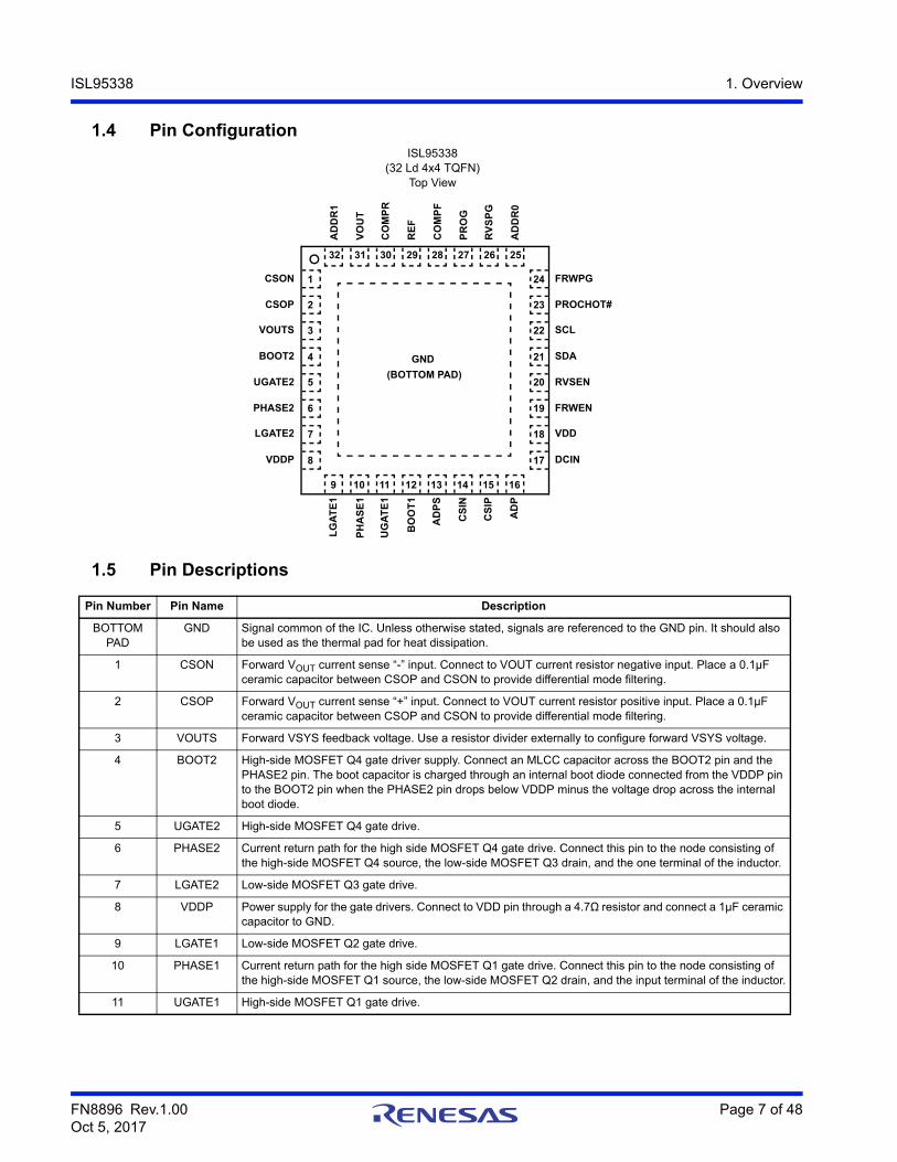
1.4 Pin ConfigurationISL95338
(32 Ld 4x4 TQFN)Top View
1.5 Pin Descriptions
Pin Number Pin Name Description
BOTTOM PAD
GND Signal common of the IC. Unless otherwise stated, signals are referenced to the GND pin. It should also be used as the thermal pad for heat dissipation.
1 CSON Forward VOUT current sense “-” input. Connect to VOUT current resistor negative input. Place a 0.1µF ceramic capacitor between CSOP and CSON to provide differential mode filtering.
2 CSOP Forward VOUT current sense “+” input. Connect to VOUT current resistor positive input. Place a 0.1µF ceramic capacitor between CSOP and CSON to provide differential mode filtering.
3 VOUTS Forward VSYS feedback voltage. Use a resistor divider externally to configure forward VSYS voltage.
4 BOOT2 High-side MOSFET Q4 gate driver supply. Connect an MLCC capacitor across the BOOT2 pin and the PHASE2 pin. The boot capacitor is charged through an internal boot diode connected from the VDDP pin to the BOOT2 pin when the PHASE2 pin drops below VDDP minus the voltage drop across the internal boot diode.
5 UGATE2 High-side MOSFET Q4 gate drive.
6 PHASE2 Current return path for the high side MOSFET Q4 gate drive. Connect this pin to the node consisting of the high-side MOSFET Q4 source, the low-side MOSFET Q3 drain, and the one terminal of the inductor.
7 LGATE2 Low-side MOSFET Q3 gate drive.
8 VDDP Power supply for the gate drivers. Connect to VDD pin through a 4.7Ω resistor and connect a 1µF ceramic capacitor to GND.
9 LGATE1 Low-side MOSFET Q2 gate drive.
10 PHASE1 Current return path for the high side MOSFET Q1 gate drive. Connect this pin to the node consisting of the high-side MOSFET Q1 source, the low-side MOSFET Q2 drain, and the input terminal of the inductor.
11 UGATE1 High-side MOSFET Q1 gate drive.
AD
DR
1
VO
UT
CO
MP
R
RE
F
CO
MP
F
PR
OG
RV
SP
G
AD
DR
0
LG
AT
E1
PH
AS
E1
UG
AT
E1
BO
OT
1
AD
PS
CS
IN
CS
IP
AD
P
CSON
CSOP
VOUTS
BOOT2
UGATE2
PHASE2
LGATE2
VDDP
FRWPG
PROCHOT#
SCL
SDA
RVSEN
FRWEN
VDD
DCIN
1
2
3
4
5
6
7
8
24
23
22
21
20
19
18
17
32 31 30 29 28 27 26 25
9 10 11 12 13 14 15 16
GND
(BOTTOM PAD)
FN8896 Rev.1.00 Page 8 of 48Oct 5, 2017
ISL95338 1. Overview
12 BOOT1 High-side MOSFET Q1 gate driver supply. Connect an MLCC capacitor across the BOOT1 pin and the PHASE1 pin. The boot capacitor is charged through an internal boot diode connected from the VDDP pin to the BOOT1 pin when the PHASE1 pin drops below VDDP minus the voltage drop across the internal boot diode.
13 ADPS Reverse output voltage feedback. Use a resistor divider externally to configure the reverse output voltage.
14 CSIN ADP current sense “-” input.
15 CSIP ADP current sense “+” input. The modulator also uses this for sensing input voltage in Forward mode and output voltage in Reverse mode.
16 ADP Used to sense ADP voltage. When ADP voltage is higher than 4.1V, Forward mode can be enabled.The ADP pin is also one of the two internal low power LDO inputs.
17 DCIN Input of an internal LDO providing power to the IC. Connect a diode OR from ADP and system outputs. Bypass this pin with an MLCC capacitor.
18 VDD Output of the internal LDO; provide the bias power for the internal analog and digital circuit. Connect a 1µF ceramic capacitor to GND.If VDD is pulled below 2.7V, the ISL95338 will reset all the SMBus register values to the default.
19 FRWEN Forward mode enable, analog signal input. Forward mode is valid if the FRWEN pin voltage is greater than 0.8V.
20 RVSEN Reverse mode enable, digital signal input. Reverse mode is valid if the signal is “1” (logic high), otherwise, Reverse mode is disabled.
21 SDA SMBus data I/O. Connect to the data line from the host controller. Connect a 10k pull-up resistor according to the SMBus specification.
22 SCL SMBus clock I/O. Connect to the clock line from the host controller. Connect a 10k pull-up resistor according to the SMBus specification.
23 PROCHOT# Open-drain output. Pulled low when input currentis detected as hot in Forward and Reverse mode. SMBus command to pull low (refer to Table 8 on page 25 and Table 10 on page 26 for Control 2 Register 0x3DH and Control4 Register 0x4EH).
24 FRWPG Open-drain output. Indicator output to indicate the forward modulator is enabled.
25 ADDR0 Address setting pin for the IC. The IC address is set by ADDR0 and ADDR1 logic voltage levels.
26 RVSPG Open-drain output. Indicator output to indicate the reverse modulator is enabled.
27 PROG A resistor from PROG pin to GND sets the default forward system output voltage.
28 COMPF Forward mode error amplifier output. Connect a compensation network externally from COMPF to GND.
29 REF Output voltage soft-start reference. A ceramic capacitor from REF to GND is set to the desired soft-start time. In Forward mode, forward output voltage (VOUTS) reference soft-start time is set. In Reverse mode, reverse output voltage (ADPS) reference soft-start time is set.
30 COMPR Reverse mode error amplifier output. Connect a compensation network externally from COMPR to GND.
31 VOUT Forward VOUT sense voltage for modulator and PHASE 2 zero-current comparator.
32 ADDR1 Address setting pin for the IC. The IC address is set by ADDR0 and ADDR1 logic voltage levels.
Pin Number Pin Name Description
FN8896 Rev.1.00 Page 9 of 48Oct 5, 2017
ISL95338 2. Specifications
2. Specifications
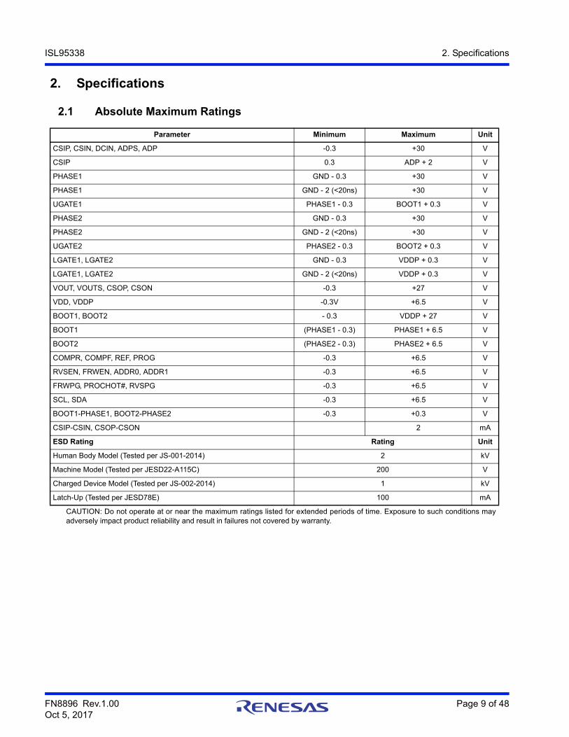
2.1 Absolute Maximum Ratings
Parameter Minimum Maximum Unit
CSIP, CSIN, DCIN, ADPS, ADP -0.3 +30 V
CSIP 0.3 ADP + 2 V
PHASE1 GND - 0.3 +30 V
PHASE1 GND - 2 (<20ns) +30 V
UGATE1 PHASE1 - 0.3 BOOT1 + 0.3 V
PHASE2 GND - 0.3 +30 V
PHASE2 GND - 2 (<20ns) +30 V
UGATE2 PHASE2 - 0.3 BOOT2 + 0.3 V
LGATE1, LGATE2 GND - 0.3 VDDP + 0.3 V
LGATE1, LGATE2 GND - 2 (<20ns) VDDP + 0.3 V
VOUT, VOUTS, CSOP, CSON -0.3 +27 V
VDD, VDDP -0.3V +6.5 V
BOOT1, BOOT2 - 0.3 VDDP + 27 V
BOOT1 (PHASE1 - 0.3) PHASE1 + 6.5 V
BOOT2 (PHASE2 - 0.3) PHASE2 + 6.5 V
COMPR, COMPF, REF, PROG -0.3 +6.5 V
RVSEN, FRWEN, ADDR0, ADDR1 -0.3 +6.5 V
FRWPG, PROCHOT#, RVSPG -0.3 +6.5 V
SCL, SDA -0.3 +6.5 V
BOOT1-PHASE1, BOOT2-PHASE2 -0.3 +0.3 V
CSIP-CSIN, CSOP-CSON 2 mA
ESD Rating Rating Unit
Human Body Model (Tested per JS-001-2014) 2 kV
Machine Model (Tested per JESD22-A115C) 200 V
Charged Device Model (Tested per JS-002-2014) 1 kV
Latch-Up (Tested per JESD78E) 100 mA
CAUTION: Do not operate at or near the maximum ratings listed for extended periods of time. Exposure to such conditions mayadversely impact product reliability and result in failures not covered by warranty.
FN8896 Rev.1.00 Page 10 of 48Oct 5, 2017
ISL95338 2. Specifications
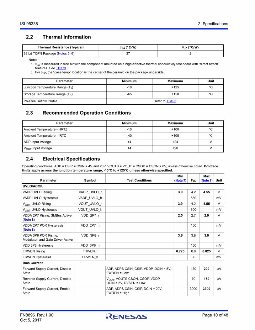
2.2 Thermal Information
2.3 Recommended Operation Conditions
2.4 Electrical Specifications
Thermal Resistance (Typical) JA (°C/W) JC (°C/W)
32 Ld TQFN Package (Notes 5, 6) 37 2
Notes:5. JA is measured in free air with the component mounted on a high-effective thermal conductivity test board with “direct attach”
features. See TB379.6. For JC, the “case temp” location is the center of the ceramic on the package underside.
Parameter Minimum Maximum Unit
Junction Temperature Range (TJ) -10 +125 °C
Storage Temperature Range (TS) -65 +150 °C
Pb-Free Reflow Profile Refer to TB493
Parameter Minimum Maximum Unit
Ambient Temperature - HRTZ -10 +100 °C
Ambient Temperature - IRTZ -40 +100 °C
ADP Input Voltage +4 +24 V
VOUT Input Voltage +4 +20 V
Operating conditions: ADP = CSIP = CSIN = 4V and 23V, VOUTS = VOUT = CSOP = CSON = 8V, unless otherwise noted. Boldface limits apply across the junction temperature range, -10°C to +125°C unless otherwise specified.
Parameter Symbol Test ConditionsMin
(Note 7) TypMax
(Note 7) Unit
UVLO/ACOK
VADP UVLO Rising VADP_UVLO_r 3.9 4.2 4.55 V
VADP UVLO Hysteresis VADP_UVLO_h 530 mV
VOUT UVLO Rising VOUT_UVLO_r 3.9 4.2 4.55 V
VOUT UVLO Hysteresis VOUT_UVLO_h 300 mV
VDDA 2P7 Rising, SMBus Active (Note 8)
VDD_2P7_r 2.5 2.7 2.9 V
VDDA 2P7 POR Hysteresis (Note 8)
VDD_2P7_h 150 mV
VDDA 3P8 POR Rising, Modulator, and Gate Driver Active
VDD_3P8_r 3.6 3.8 3.9 V
VDD 3P8 Hysteresis VDD_3P8_h 150 mV
FRWEN Rising FRWEN_r 0.775 0.8 0.825 V
FRWEN Hysteresis FRWEN_h 50 mV
Bias Current
Forward Supply Current, Disable State
ADP, ADPS CSIN, CSIP, VDDP, DCIN = 5V, FWREN = Low
130 200 µA
Reverse Supply Current, Disable State
VOUT, VOUTS CSON, CSOP, VDDP, DCIN = 5V, RVSEN = Low
70 150 µA
Forward Supply Current, Enable State
ADP, ADPS CSIN, CSIP, DCIN = 20V, FWREN = High
3000 3300 µA
FN8896 Rev.1.00 Page 11 of 48Oct 5, 2017
ISL95338 2. Specifications
Reverse Supply Current, Enable State
VOUT, VOUTS CSON, CSOP, DCIN = 20V, RVSEN = High
3000 3300 µA
Forward Supply Current, Enable State
DCIN only (does not include gate driver current)
1600 2000 µA
Reverse Supply Current, Enable State
DCIN only (does not include gate driver current)
1600 2000 µA
Linear Regulator
VDDA Output Voltage VDD 6V < VADP < 23V, no load 4.5 5.1 5.5 V
VDDA Dropout Voltage VDD_dp 30mA, VDCIN = 4V 100 mV
VDD Overcurrent Threshold VDD_OC 90 135 165 mA
ADP Current Regulation, RADP = 20mΩ
Input Current Accuracy |CSIP - CSIN| = 80mV 4 A
-3 +3 %
|CSIP - CSIN| = 40mV 2 A
-4 +4 %
|CSIP - CSIN| = 10mV 0.5 A
-10 +10 %
ADP Current PROCHOT# ThresholdRs1 = 20mΩ
IADP_HOT_TH10 ACProchot = 0x0A80H (2688mA) 2688 mA
-3.0 +3.0 %
ACProchot = 0x0400H (1024mA) 1024 mA
-6.0 +6.0 %
Voltage Regulation
Output Voltage Accuracy Forward HRTZ Measured at VOUTS, 8V and up -1 +1 %
Output Voltage Accuracy Forward HRTZ Measured at VOUTS, 4V to 8V -1.5 +1.5 %
Output Voltage Accuracy Reverse HRTZ Measured at ADPS, 8V and up -1 +1 %
Output Voltage Accuracy Reverse HRTZ Measured at ADPS, 4V to 8V -1.5 +1.5 %
Output Voltage Accuracy Forward IRTZ Measured at VOUTS, 8V and up -2 +2 %
Output Voltage Accuracy Forward IRTZ Measured at VOUTS, 4V to 8V -1.5 +1.5 %
Output Voltage Accuracy Reverse IRTZ Measured at ADPS, 8V and up -2 +2 %
Output Voltage Accuracy Reverse IRTZ Measured at ADPS, 4V to 8V -3 +3 %
Minimum Input Voltage Accuracy Measured at ADPS -3 +3 V
VOUT Current Regulation, Rs2 = 10mΩ
VOUT Current Accuracy |CSOP - CSON| = 60mV 6 A
-3 +3 %
|CSOP - CSON| = 20mV 2 A
-5 +5 %
|CSOP - CSON| = 10mV 1 A
-10 +10 %
|CSOP - CSON| = 5mV 0.5 A
-20 +20 %
ADP Current-Sense Amplifier, RADP = 20mΩ
CSIP/CSIN Input Voltage Range VCSIP/N 0 27 V
Operating conditions: ADP = CSIP = CSIN = 4V and 23V, VOUTS = VOUT = CSOP = CSON = 8V, unless otherwise noted. Boldface limits apply across the junction temperature range, -10°C to +125°C unless otherwise specified. (Continued)
Parameter Symbol Test ConditionsMin
(Note 7) TypMax
(Note 7) Unit
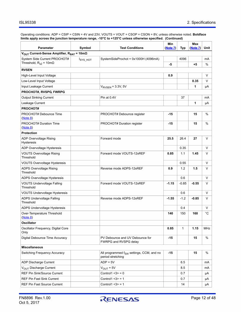
FN8896 Rev.1.00 Page 12 of 48Oct 5, 2017
ISL95338 2. Specifications
VOUT Current-Sense Amplifier, RBAT = 10mΩ
System Side Current PROCHOT# Threshold, Rs2 = 10mΩ
ISYS_HOT SystemSideProchot = 0x1000H (4096mA) 4096 mA
-5 +5 %
RVSEN
High-Level Input Voltage 0.9 V
Low-Level Input Voltage 0.35 V
Input Leakage Current VRVSEN = 3.3V, 5V 1 µA
PROCHOT#, RVSPG, FWRPG
Output Sinking Current Pin at 0.4V 37 mA
Leakage Current 1 µA
PROCHOT#
PROCHOT# Debounce Time (Note 8)
PROCHOT# Debounce register -15 15 %
PROCHOT# Duration Time (Note 8)
PROCHOT# Duration register -15 15 %
Protection
ADP Overvoltage Rising Hysteresis
Forward mode 25.5 26.4 27 V
ADP Overvoltage Hysteresis 0.35 V
VOUTS Overvoltage Rising Threshold
Forward mode VOUTS-12xREF 0.85 1.1 1.45 V
VOUTS Overvoltage Hysteresis 0.55 V
ADPS Overvoltage Rising Threshold
Reverse mode ADPS-12xREF 0.9 1.2 1.5 V
ADPS Overvoltage Hysteresis 0.6 V
VOUTS Undervoltage Falling Threshold
Forward mode VOUTS-12xREF -1.15 -0.85 -0.55 V
VOUTS Undervoltage Hysteresis 0.6 V
ADPS Undervoltage Falling Threshold
Reverse mode ADPS-12xREF -1.55 -1.2 -0.85 V
ADPS Undervoltage Hysteresis 0.4 V
Over-Temperature Threshold (Note 8)
140 150 160 °C
Oscillator
Oscillator Frequency, Digital Core Only
0.85 1 1.15 MHz
Digital Debounce Time Accuracy PV Debounce and UV Debounce for FWRPG and RVSPG delay
-15 15 %
Miscellaneous
Switching Frequency Accuracy All programmed fSW settings, CCM, and no period stretching
-15 15 %
ADP Discharge Current ADP = 5V 6.5 mA
VOUT Discharge Current VOUT = 5V 8.5 mA
REF Pin Sink/Source Current Control1 <3> = 0 0.7 µA
REF Pin Fast Sink Current Control1 <3> = 1 0.7 µA
REF Pin Fast Source Current Control1 <3> = 1 14 µA
Operating conditions: ADP = CSIP = CSIN = 4V and 23V, VOUTS = VOUT = CSOP = CSON = 8V, unless otherwise noted. Boldface limits apply across the junction temperature range, -10°C to +125°C unless otherwise specified. (Continued)
Parameter Symbol Test ConditionsMin
(Note 7) TypMax
(Note 7) Unit
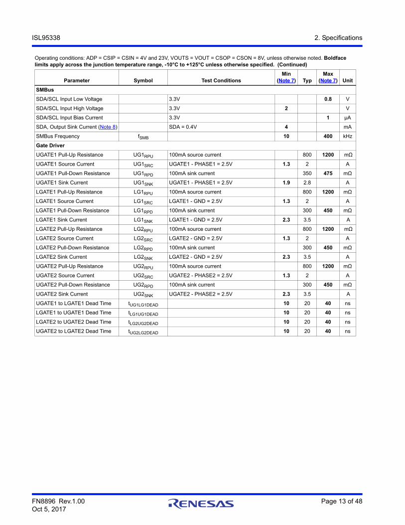
FN8896 Rev.1.00 Page 13 of 48Oct 5, 2017
ISL95338 2. Specifications
SMBus
SDA/SCL Input Low Voltage 3.3V 0.8 V
SDA/SCL Input High Voltage 3.3V 2 V
SDA/SCL Input Bias Current 3.3V 1 µA
SDA, Output Sink Current (Note 8) SDA = 0.4V 4 mA
SMBus Frequency fSMB 10 400 kHz
Gate Driver
UGATE1 Pull-Up Resistance UG1RPU 100mA source current 800 1200 mΩ
UGATE1 Source Current UG1SRC UGATE1 - PHASE1 = 2.5V 1.3 2 A
UGATE1 Pull-Down Resistance UG1RPD 100mA sink current 350 475 mΩ
UGATE1 Sink Current UG1SNK UGATE1 - PHASE1 = 2.5V 1.9 2.8 A
LGATE1 Pull-Up Resistance LG1RPU 100mA source current 800 1200 mΩ
LGATE1 Source Current LG1SRC LGATE1 - GND = 2.5V 1.3 2 A
LGATE1 Pull-Down Resistance LG1RPD 100mA sink current 300 450 mΩ
LGATE1 Sink Current LG1SNK LGATE1 - GND = 2.5V 2.3 3.5 A
LGATE2 Pull-Up Resistance LG2RPU 100mA source current 800 1200 mΩ
LGATE2 Source Current LG2SRC LGATE2 - GND = 2.5V 1.3 2 A
LGATE2 Pull-Down Resistance LG2RPD 100mA sink current 300 450 mΩ
LGATE2 Sink Current LG2SNK LGATE2 - GND = 2.5V 2.3 3.5 A
UGATE2 Pull-Up Resistance UG2RPU 100mA source current 800 1200 mΩ
UGATE2 Source Current UG2SRC UGATE2 - PHASE2 = 2.5V 1.3 2 A
UGATE2 Pull-Down Resistance UG2RPD 100mA sink current 300 450 mΩ
UGATE2 Sink Current UG2SNK UGATE2 - PHASE2 = 2.5V 2.3 3.5 A
UGATE1 to LGATE1 Dead Time tUG1LG1DEAD 10 20 40 ns
LGATE1 to UGATE1 Dead Time tLG1UG1DEAD 10 20 40 ns
LGATE2 to UGATE2 Dead Time tLG2UG2DEAD 10 20 40 ns
UGATE2 to LGATE2 Dead Time tUG2LG2DEAD 10 20 40 ns
Operating conditions: ADP = CSIP = CSIN = 4V and 23V, VOUTS = VOUT = CSOP = CSON = 8V, unless otherwise noted. Boldface limits apply across the junction temperature range, -10°C to +125°C unless otherwise specified. (Continued)
Parameter Symbol Test ConditionsMin
(Note 7) TypMax
(Note 7) Unit
FN8896 Rev.1.00 Page 14 of 48Oct 5, 2017
ISL95338 2. Specifications
2.5 SMBus Timing Specification
Figure 4. Gate Driver Timing Diagram
Parameters Symbol Test ConditionsMin
(Note 7) TypMax
(Note 7) Unit
SMBus Frequency FSMB 10 400 kHz
Bus-Free Time tBUF 4.7 µs
Start Condition Hold Time from SCL tHD:STA 4 µs
Start Condition Set-Up Time from SCL
tSU:STA 4.7 µs
Stop Condition Set-Up Time from SCL
tSU:STO 4 µs
SDA Hold Time from SCL tHD:DAT 300 ns
SDA Set-Up Time from SCL tSU:DAT 250 ns
SCL Low Period tLOW 4.7 µs
SCL High Period tHIGH 4 µs
SMBus Inactivity Timeout Maximum charging period without an SMBus Write to MaxSystemVoltage or ADPCurrent register
175 s
Notes:7. Parameters with MIN and/or MAX limits are 100% tested at +25°C, unless otherwise specified. Temperature limits established by
characterization and are not production tested.8. Compliance to datasheet limits is assured by one or more methods: production test, characterization, and/or design.
PWM
UGATE
LGATE 1V
1V
tUGFLGR
tRL
tFUtRU
tFL
tLGFUGR
FN8896 Rev.1.00 Page 15 of 48Oct 5, 2017
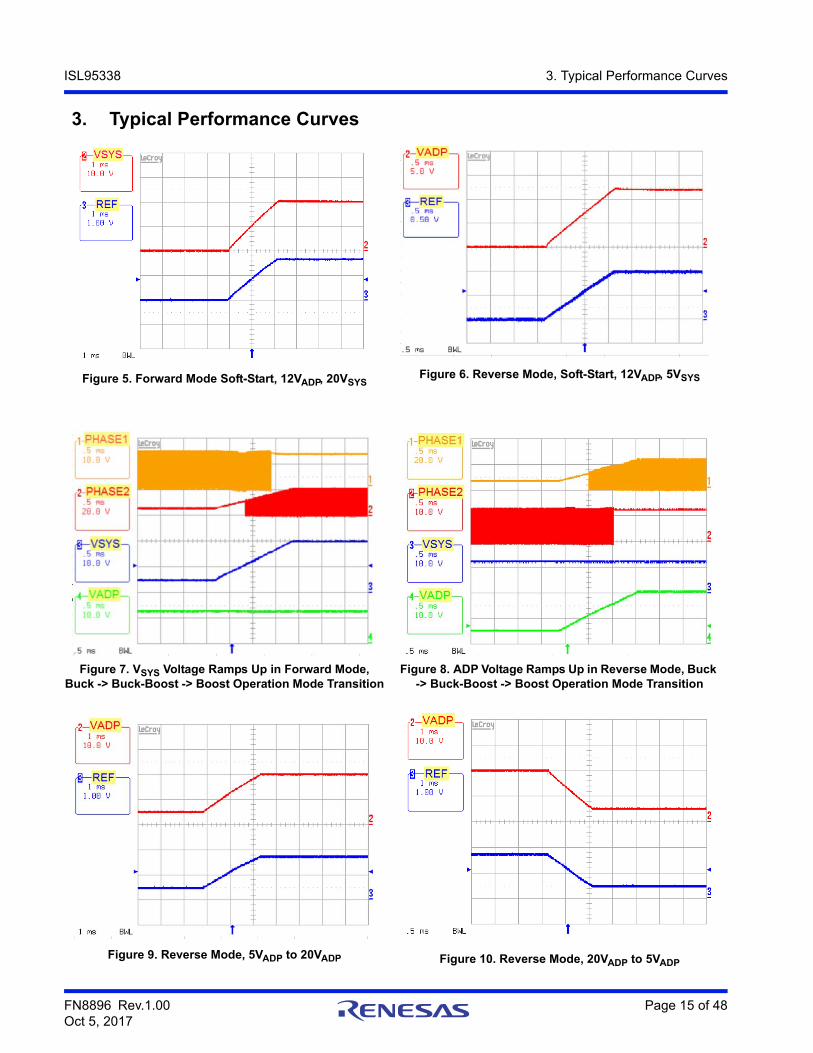
ISL95338 3. Typical Performance Curves
3. Typical Performance Curves
Figure 5. Forward Mode Soft-Start, 12VADP, 20VSYSFigure 6. Reverse Mode, Soft-Start, 12VADP, 5VSYS
Figure 7. VSYS Voltage Ramps Up in Forward Mode, Buck -> Buck-Boost -> Boost Operation Mode Transition
Figure 8. ADP Voltage Ramps Up in Reverse Mode, Buck -> Buck-Boost -> Boost Operation Mode Transition
Figure 9. Reverse Mode, 5VADP to 20VADP Figure 10. Reverse Mode, 20VADP to 5VADP
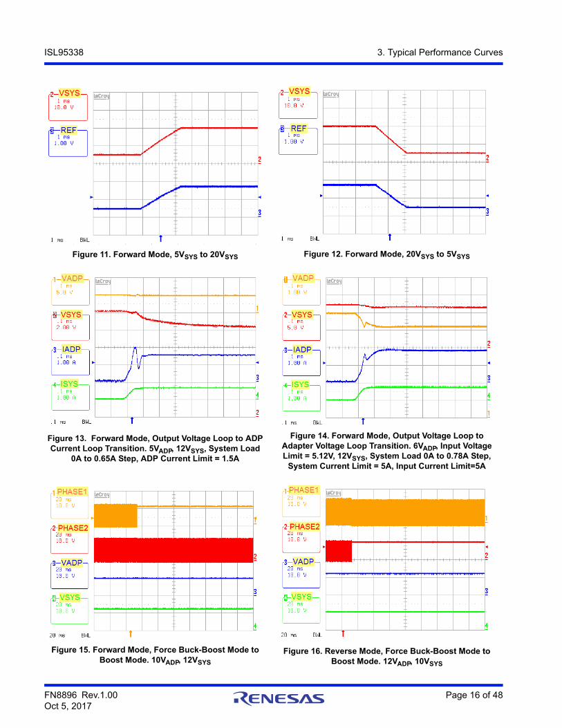
FN8896 Rev.1.00 Page 16 of 48Oct 5, 2017
ISL95338 3. Typical Performance Curves
Figure 11. Forward Mode, 5VSYS to 20VSYS Figure 12. Forward Mode, 20VSYS to 5VSYS
Figure 13. Forward Mode, Output Voltage Loop to ADP Current Loop Transition. 5VADP, 12VSYS, System Load
0A to 0.65A Step, ADP Current Limit = 1.5A
Figure 14. Forward Mode, Output Voltage Loop to Adapter Voltage Loop Transition. 6VADP, Input Voltage Limit = 5.12V, 12VSYS, System Load 0A to 0.78A Step,
System Current Limit = 5A, Input Current Limit=5A
Figure 15. Forward Mode, Force Buck-Boost Mode to Boost Mode. 10VADP, 12VSYS
Figure 16. Reverse Mode, Force Buck-Boost Mode to Boost Mode. 12VADP, 10VSYS
FN8896 Rev.1.00 Page 17 of 48Oct 5, 2017
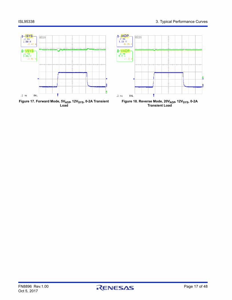
ISL95338 3. Typical Performance Curves
Figure 17. Forward Mode, 5VADP, 12VSYS, 0-2A Transient Load
Figure 18. Reverse Mode, 20VADP, 12VSYS, 0-2A Transient Load
FN8896 Rev.1.00 Page 18 of 48Oct 5, 2017
ISL95338 4. General SMBus Architecture
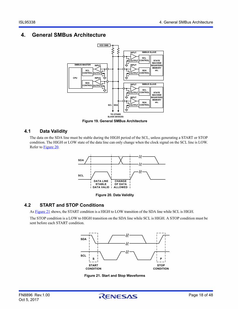
4. General SMBus Architecture
Figure 19. General SMBus Architecture
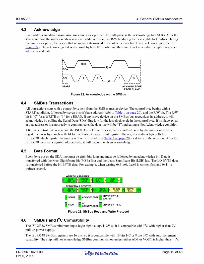
4.1 Data ValidityThe data on the SDA line must be stable during the HIGH period of the SCL, unless generating a START or STOP condition. The HIGH or LOW state of the data line can only change when the clock signal on the SCL line is LOW. Refer to Figure 20.
Figure 20. Data Validity
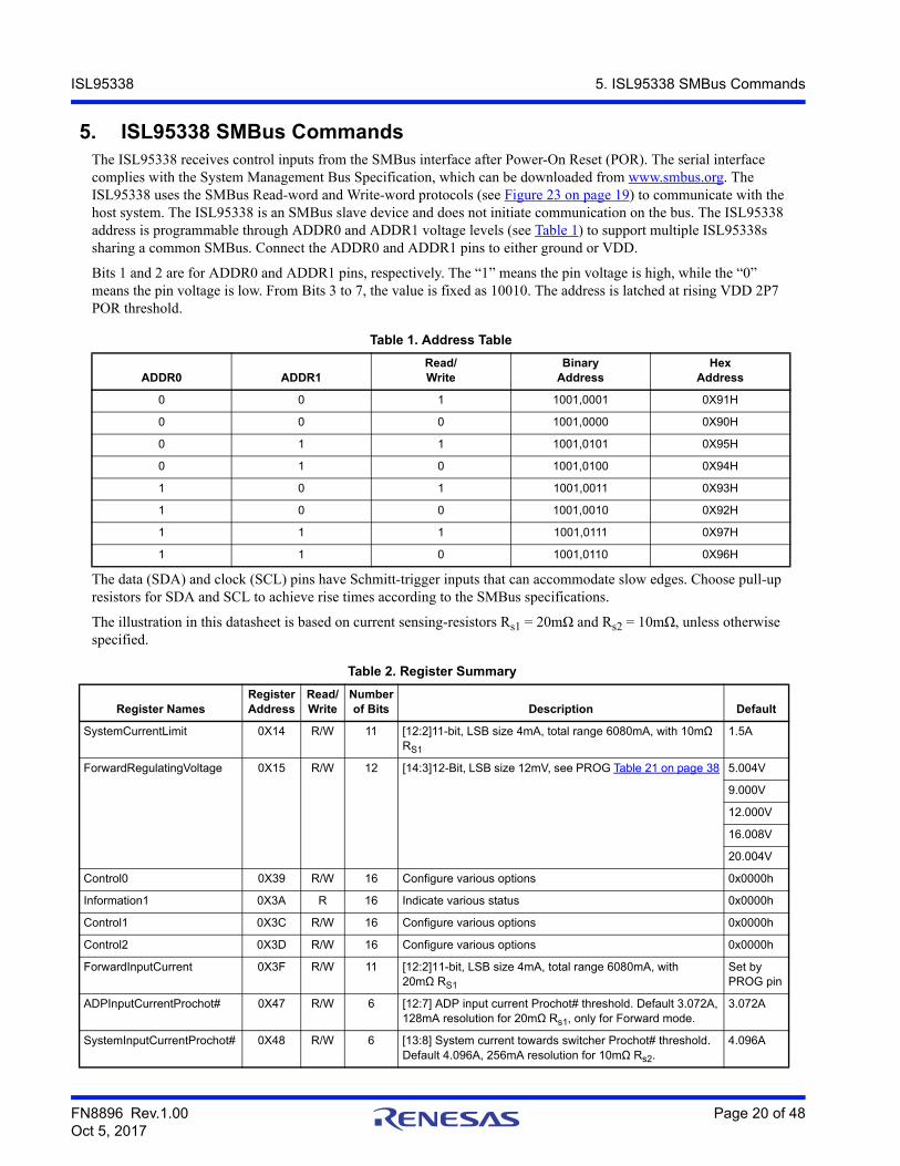
4.2 START and STOP ConditionsAs Figure 21 shows, the START condition is a HIGH to LOW transition of the SDA line while SCL is HIGH.
The STOP condition is a LOW to HIGH transition on the SDA line while SCL is HIGH. A STOP condition must be sent before each START condition.
Figure 21. Start and Stop Waveforms
SCLCONTROLOUTPUT
SDACONTROLOUTPUT
INPUT
INPUT
STATEMACHINE
REGISTERSMEMORY
etc.
SMBUS SLAVE
SCLCONTROLOUTPUT
SDACONTROLOUTPUT
INPUT
INPUT
STATEMACHINE
REGISTERSMEMORY
etc.
SMBUS SLAVE
SCLCONTROL OUTPUT
SDACONTROL OUTPUT
INPUT
INPUTCPU
SMBUS MASTER
TO OTHER SLAVE DEVICES
VDD SMB
SCL SDA
SDA
SCL
DATA LINESTABLE
DATA VALID
CHANGEOF DATA
ALLOWED
SDA
SCLS
STARTCONDITION
P
STOPCONDITION
FN8896 Rev.1.00 Page 19 of 48Oct 5, 2017
ISL95338 4. General SMBus Architecture
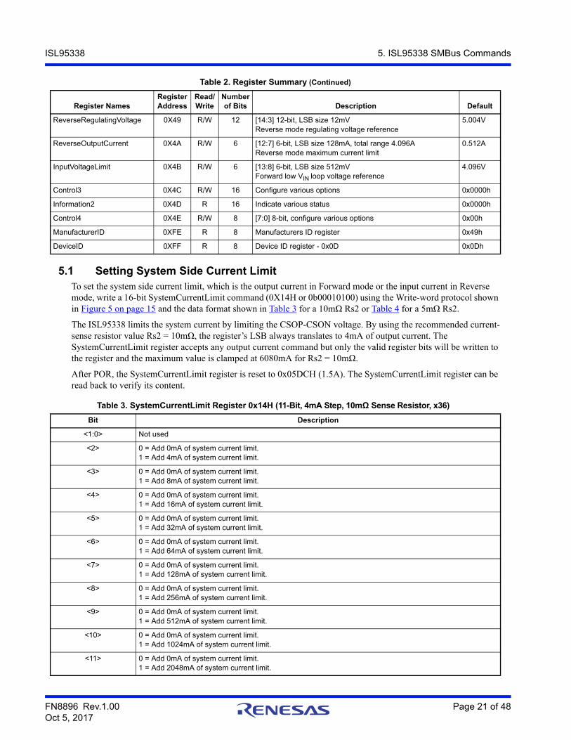
4.3 AcknowledgeEach address and data transmission uses nine clock pulses. The ninth pulse is the acknowledge bit (ACK). After the start condition, the master sends seven slave address bits and an R/W bit during the next eight clock pulses. During the nine clock pulse, the device that recognizes its own address holds the data line low to acknowledge (refer to Figure 22). The acknowledge bit is also used by both the master and the slave to acknowledge receipt of register addresses and data.
Figure 22. Acknowledge on the SMBus
4.4 SMBus TransactionsAll transactions start with a control byte sent from the SMBus master device. The control byte begins with a START condition, followed by seven bits of slave address (refer to Table 1 on page 20), and the R/W bit. The R/W bit is “0” for a WRITE or “1” for a READ. If any slave device on the SMBus bus recognizes its address, it will acknowledge by pulling the Serial Data (SDA) line low for the last clock cycle in the control byte. If no slave exists at that address or it is not ready to communicate, the data line will be “1”, indicating a Not Acknowledge condition.
After the control byte is sent and the ISL95338 acknowledges it, the second byte sent by the master must be a register address byte such as 0x14 for the SystemCurrentLimit register. The register address byte tells the ISL95338 which register the master will write or read. See Table 2 on page 20 for details of the registers. After the ISL95338 receives a register address byte, it will respond with an acknowledge.
4.5 Byte FormatEvery byte put on the SDA line must be eight bits long and must be followed by an acknowledge bit. Data is transferred with the Most Significant Bit (MSB) first and the Least Significant Bit (LSB) last. The LO BYTE data is transferred before the HI BYTE data. For example, when writing 0x41A0, 0xA0 is written first and 0x41 is written second.
Figure 23. SMBus Read and Write Protocol
4.6 SMBus and I2C CompatibilityThe ISL95338 SMBus minimum input logic high voltage is 2V, so it is compatible with I2C with higher than 2V pull-up power supply.
The ISL95338 SMBus registers are 16 bits, so it is compatible with 16 bits I2C or 8 bits I2C with auto-increment capability. The chip will not acknowledge SMBus communication unless either ADP or VOUT is higher than 4.1V.
SDA
SCL
START ACKNOWLEDGEFROM SLAVE
1 2 8 9
MSB
SSLAVE
ADDR + WA
REGISTERADDR
ALO BYTE
DATAA
HI BYTE DATA
A P
WRITE TO A REGISTER
SSLAVE
ADDR + WA
REGISTERADDR
A
READ FROM A REGISTER
P SSLAVE
ADDR + RA
LO BYTE DATA
AHI BYTE DATA
N P
S START
P STOP
A ACKNOWLEDGE
NNO ACKNOWLEDGE
DRIVEN BY THE MASTER
P DRIVEN BY THE IC
FN8896 Rev.1.00 Page 20 of 48Oct 5, 2017
ISL95338 5. ISL95338 SMBus Commands
5. ISL95338 SMBus CommandsThe ISL95338 receives control inputs from the SMBus interface after Power-On Reset (POR). The serial interface complies with the System Management Bus Specification, which can be downloaded from www.smbus.org. The ISL95338 uses the SMBus Read-word and Write-word protocols (see Figure 23 on page 19) to communicate with the host system. The ISL95338 is an SMBus slave device and does not initiate communication on the bus. The ISL95338 address is programmable through ADDR0 and ADDR1 voltage levels (see Table 1) to support multiple ISL95338s sharing a common SMBus. Connect the ADDR0 and ADDR1 pins to either ground or VDD.
Bits 1 and 2 are for ADDR0 and ADDR1 pins, respectively. The “1” means the pin voltage is high, while the “0” means the pin voltage is low. From Bits 3 to 7, the value is fixed as 10010. The address is latched at rising VDD 2P7 POR threshold.
The data (SDA) and clock (SCL) pins have Schmitt-trigger inputs that can accommodate slow edges. Choose pull-up resistors for SDA and SCL to achieve rise times according to the SMBus specifications.
The illustration in this datasheet is based on current sensing-resistors Rs1 = 20mΩand Rs2 = 10mΩ, unless otherwise specified.
Table 1. Address Table
ADDR0 ADDR1Read/Write
BinaryAddress
HexAddress
0 0 1 1001,0001 0X91H
0 0 0 1001,0000 0X90H
0 1 1 1001,0101 0X95H
0 1 0 1001,0100 0X94H
1 0 1 1001,0011 0X93H
1 0 0 1001,0010 0X92H
1 1 1 1001,0111 0X97H
1 1 0 1001,0110 0X96H
Table 2. Register Summary
Register NamesRegister Address
Read/ Write
Number of Bits Description Default
SystemCurrentLimit 0X14 R/W 11 [12:2]11-bit, LSB size 4mA, total range 6080mA, with 10mΩ RS1
1.5A
ForwardRegulatingVoltage 0X15 R/W 12 [14:3]12-Bit, LSB size 12mV, see PROG Table 21 on page 38 5.004V
9.000V
12.000V
16.008V
20.004V
Control0 0X39 R/W 16 Configure various options 0x0000h
Information1 0X3A R 16 Indicate various status 0x0000h
Control1 0X3C R/W 16 Configure various options 0x0000h
Control2 0X3D R/W 16 Configure various options 0x0000h
ForwardInputCurrent 0X3F R/W 11 [12:2]11-bit, LSB size 4mA, total range 6080mA, with 20mΩ RS1
Set by PROG pin
ADPInputCurrentProchot# 0X47 R/W 6 [12:7] ADP input current Prochot# threshold. Default 3.072A,128mA resolution for 20mΩ Rs1, only for Forward mode.
3.072A
SystemInputCurrentProchot# 0X48 R/W 6 [13:8] System current towards switcher Prochot# threshold. Default 4.096A, 256mA resolution for 10mΩ Rs2.
4.096A
FN8896 Rev.1.00 Page 21 of 48Oct 5, 2017
ISL95338 5. ISL95338 SMBus Commands
5.1 Setting System Side Current LimitTo set the system side current limit, which is the output current in Forward mode or the input current in Reverse mode, write a 16-bit SystemCurrentLimit command (0X14H or 0b00010100) using the Write-word protocol shown in Figure 5 on page 15 and the data format shown in Table 3 for a 10mΩ Rs2 or Table 4 for a 5mΩ Rs2.
The ISL95338 limits the system current by limiting the CSOP-CSON voltage. By using the recommended current-sense resistor value Rs2 = 10mΩ, the register’s LSB always translates to 4mA of output current. The SystemCurrentLimit register accepts any output current command but only the valid register bits will be written to the register and the maximum value is clamped at 6080mA for Rs2 = 10mΩ.
After POR, the SystemCurrentLimit register is reset to 0x05DCH (1.5A). The SystemCurrentLimit register can be read back to verify its content.
ReverseRegulatingVoltage 0X49 R/W 12 [14:3] 12-bit, LSB size 12mVReverse mode regulating voltage reference
5.004V
ReverseOutputCurrent 0X4A R/W 6 [12:7] 6-bit, LSB size 128mA, total range 4.096AReverse mode maximum current limit
0.512A
InputVoltageLimit 0X4B R/W 6 [13:8] 6-bit, LSB size 512mVForward low VIN loop voltage reference
4.096V
Control3 0X4C R/W 16 Configure various options 0x0000h
Information2 0X4D R 16 Indicate various status 0x0000h
Control4 0X4E R/W 8 [7:0] 8-bit, configure various options 0x00h
ManufacturerID 0XFE R 8 Manufacturers ID register 0x49h
DeviceID 0XFF R 8 Device ID register - 0x0D 0x0Dh
Table 3. SystemCurrentLimit Register 0x14H (11-Bit, 4mA Step, 10mΩ Sense Resistor, x36)
Bit Description
<1:0> Not used
<2> 0 = Add 0mA of system current limit. 1 = Add 4mA of system current limit.
<3> 0 = Add 0mA of system current limit. 1 = Add 8mA of system current limit.
<4> 0 = Add 0mA of system current limit. 1 = Add 16mA of system current limit.
<5> 0 = Add 0mA of system current limit. 1 = Add 32mA of system current limit.
<6> 0 = Add 0mA of system current limit. 1 = Add 64mA of system current limit.
<7> 0 = Add 0mA of system current limit. 1 = Add 128mA of system current limit.
<8> 0 = Add 0mA of system current limit. 1 = Add 256mA of system current limit.
<9> 0 = Add 0mA of system current limit. 1 = Add 512mA of system current limit.
<10> 0 = Add 0mA of system current limit. 1 = Add 1024mA of system current limit.
<11> 0 = Add 0mA of system current limit. 1 = Add 2048mA of system current limit.
Table 2. Register Summary (Continued)
Register NamesRegister Address
Read/ Write
Number of Bits Description Default
FN8896 Rev.1.00 Page 22 of 48Oct 5, 2017
ISL95338 5. ISL95338 SMBus Commands
5.2 Setting Input Current Limit in Forward ModeTo set the input current limit in Forward mode, write a 16-bit ForwardInputCurrent command (0x3FH or 0b00111111) using the Write-word protocol shown in Figure 5 on page 15 and the data format shown in Table 5 for a 20mΩ Rs1 or Table 6 on page 23 for a 10mΩ Rs1.
The ISL95338 limits the input current in Forward mode by limiting the CSIP-CSIN voltage. By using the recommended current-sense resistor values, the register’s LSB always translates to 4mA of input current. Any input current limit command will be accepted but only the valid register bits will be written to the ForwardInputCurrent register and the maximum values are clamped at 6080mA for Rs1 = 20mΩ.
<12> 0 = Add 0mA of system current limit. 1 = Add 4096mA of system current limit.
<13:15> Not used
Maximum <12:2> = 10111110000 6080mA
Note: The gain for the system side current-sensing amplifiers is different for Forward mode and Reverse mode. The gain in Reversemode is half of that in Forward mode. Therefore, in Reverse mode, the sensing current value needs to be doubled compared to thevalue set in the SystemCurrentLimit register.
Table 4. ForwardOutputCurrentLimit Register 0x14H (11-Bit, 8mA Step, 5mΩ Sense Resistor, x36)
Bit Description
<1:0> Not used
<2> 0 = Add 0mA of system current limit. 1 = Add 8mA of system current limit.
<3> 0 = Add 0mA of system current limit. 1 = Add 16mA of system current limit.
<4> 0 = Add 0mA of system current limit. 1 = Add 32mA of system current limit.
<5> 0 = Add 0mA of system current limit. 1 = Add 64mA of system current limit.
<6> 0 = Add 0mA of system current limit. 1 = Add 128mA of system current limit.
<7> 0 = Add 0mA of system current limit. 1 = Add 256mA of system current limit.
<8> 0 = Add 0mA of system current limit. 1 = Add 512mA of system current limit.
<9> 0 = Add 0mA of system current limit. 1 = Add 1024mA of system current limit.
<10> 0 = Add 0mA of system current limit. 1 = Add 2048mA of system current limit.
<11> 0 = Add 0mA of system current limit.1 = Add 4096mA of system current limit.
<12> 0 = Add 0mA of system current limit. 1 = Add 8192mA of system current limit.
<13:15> Not used
Maximum <12:2> = 10111110000 12160mA
Table 3. SystemCurrentLimit Register 0x14H (11-Bit, 4mA Step, 10mΩ Sense Resistor, x36) (Continued)
Bit Description
FN8896 Rev.1.00 Page 23 of 48Oct 5, 2017
ISL95338 5. ISL95338 SMBus Commands
.
Table 5. ForwardInputCurrent Register 0x3FH (11-Bit, 4mA Step, 20mΩ Sense Resistor, x18)
Bit Description
<1:0> Not used
<2> 0 = Add 0mA of input current limit in Forward mode. 1 = Add 4mA of input current limit in Forward mode.
<3> 0 = Add 0mA of input current limit in Forward mode. 1 = Add 8mA of input current limit in Forward mode.
<4> 0 = Add 0mA of input current limit in Forward mode. 1 = Add 16mA of input current limit in Forward mode.
<5> 0 = Add 0mA of input current limit in Forward mode. 1 = Add 32mA of input current limit in Forward mode.
<6> 0 = Add 0mA of input current limit in Forward mode. 1 = Add 64mA of input current limit in Forward mode.
<7> 0 = Add 0mA of input current limit in Forward mode. 1 = Add 128mA of input current limit in Forward mode.
<8> 0 = Add 0mA of input current limit in Forward mode. 1 = Add 256mA of input current limit in Forward mode.
<9> 0 = Add 0mA of input current limit in Forward mode. 1 = Add 512mA of input current limit in Forward mode.
<10> 0 = Add 0mA of input current limit in Forward mode. 1 = Add 1024mA of input current limit in Forward mode.
<11> 0 = Add 0mA of input current limit in Forward mode. 1 = Add 2048mA of input current limit in Forward mode.
<12> 0 = Add 0mA of input current limit in Forward mode. 1 = Add 4096mA of input current limit in Forward mode.
<13:15> Not used
Maximum <12:4> = 10111110000 6080mA.
Table 6. ForwardInputCurrent Register 0x3FH (11-BIT, 8mA STEP, 10mΩ Sense Resistor, x18)
Bit Description
<1:0> Not used
<2> 0 = Add 0mA of input current limit in Forward mode. 1 = Add 8mA of input current limit in Forward mode.
<3> 0 = Add 0mA of input current limit in Forward mode. 1 = Add 16mA of input current limit in Forward mode.
<4> 0 = Add 0mA of input current limit in Forward mode. 1 = Add 32mA of input current limit in Forward mode.
<5> 0 = Add 0mA of input current limit in Forward mode. 1 = Add 64mA of input current limit in Forward mode.
<6> 0 = Add 0mA of input current limit in Forward mode. 1 = Add 128mA of input current limit in Forward mode.
<7> 0 = Add 0mA of input current limit in Forward mode. 1 = Add 256mA of input current limit in Forward mode.
<8> 0 = Add 0mA of input current limit in Forward mode. 1 = Add 512mA of input current limit in Forward mode.
<9> 0 = Add 0mA of input current limit in Forward mode. 1 = Add 1024mA of input current limit in Forward mode.
<10> 0 = Add 0mA of input current limit in Forward mode. 1 = Add 2048mA of input current limit in Forward mode.
FN8896 Rev.1.00 Page 24 of 48Oct 5, 2017
ISL95338 5. ISL95338 SMBus Commands
5.3 Setting System Regulating Voltage in Forward ModeTo set the regulating voltage in Forward mode, write a 16-bit ForwardRegulatingVoltage command (0x15H or 0b00010101) using the Write-word protocol shown in Figure 5 on page 15 and the data format as shown in Table 7.
The output regulating voltage range in Forward mode is 2V to 24V. The ForwardRegulatingVoltage register accepts any voltage command, but only the valid register bits will be written to the register. The maximum value is clamped at 24.576V. The ISL95338 accepts a 0V command, but the register value does not change. The VOUTS pin is the output voltage regulation sense point in Forward mode.
In Forward mode, the customer also can configure the regulating output voltage by setting the external voltage divider on the VOUTS pin without changing the ForwardRegulatingVoltage register value.
<11> 0 = Add 0mA of input current limit in Forward mode. 1 = Add 4096mA of input current limit in Forward mode.
<12> 0 = Add 0mA of input current limit in Forward mode. 1 = Add 8192mA of input current limit in Forward mode.
<13:15> Not used
Maximum <12:4> = 10111110000 12160mA
Table 7. ForwardRegulatingVoltage Register 0x15H (12mV Step)
Bit Description
<2:0> Not used
<3> 0 = Add 0mV of regulating voltage in Forward mode. 1 = Add 12mV of regulating voltage in Forward mode.
<4> 0 = Add 0mV of regulating voltage in Forward mode. 1 = Add 24mV of regulating voltage in Forward mode.
<5> 0 = Add 0mV of regulating voltage in Forward mode. 1 = Add 48mV of regulating voltage in Forward mode.
<6> 0 = Add 0mV of regulating voltage in Forward mode. 1 = Add 96mV of regulating voltage in Forward mode.
<7> 0 = Add 0mV of regulating voltage in Forward mode. 1 = Add 192mV of regulating voltage in Forward mode.
<8> 0 = Add 0mV of regulating voltage in Forward mode. 1 = Add 384mV of regulating voltage in Forward mode.
<9> 0 = Add 0mV of regulating voltage in Forward mode. 1 = Add 768mV of regulating voltage in Forward mode.
<10> 0 = Add 0mV of regulating voltage in Forward mode. 1 = Add 1536mV of regulating voltage in Forward mode.
<11> 0 = Add 0mV of regulating voltage in Forward mode. 1 = Add 3072mV of regulating voltage in Forward mode.
<12> 0 = Add 0mV of regulating voltage in Forward mode. 1 = Add 6144mV of regulating voltage in Forward mode.
<13> 0 = Add 0mV of regulating voltage in Forward mode. 1 = Add 12288mV of regulating voltage in Forward mode.
<14> 0 = Add 0mV of regulating voltage in Forward mode. 1 = Add 24576mV of regulating voltage in Forward mode.
<15> Not used
Maximum 24576mV
Note: The default reading value of this register is 6.288V when the chip is powering up without writing any values because of theDAC initial value. Thus, write the needed value in this register before enabling forward output voltage.
Table 6. ForwardInputCurrent Register 0x3FH (11-BIT, 8mA STEP, 10mΩ Sense Resistor, x18) (Continued)
Bit Description
FN8896 Rev.1.00 Page 25 of 48Oct 5, 2017
ISL95338 5. ISL95338 SMBus Commands
5.4 Setting PROCHOT# Threshold for ADP Side Overcurrent ConditionTo set the PROCHOT# assertion threshold for ADP side input overcurrent condition in Forward mode, write a 16-bit ADPsideProchot# command (0x47H or 0b01000111) using the Write-word protocol shown in Table 5 on page 23 and the data format shown in Table 8. By using the recommended current-sense resistor values, the register’s LSB always translates to 128mA of input current. The ADPsideProchot# register accepts any current command, but only the valid register bits will be written to the register. The maximum values are clamped at 6400mA for Rs1 = 20mΩ.
After POR, the ADPsideProchot# register is reset to 0x0C00H. The ADPsideProchot# register can be read back to verify its content.
If the input current exceeds the ADPsideProchot# register setting, PROCHOT# signal will assert after the debounce time programmed by the Control2 register Bit<10:9> and latch on for a minimum time programmed by Control2 register Bit<8:6>.
5.5 Setting PROCHOT# Threshold for System Side Overcurrent ConditionTo set the PROCHOT# signal assertion threshold for system side input overcurrent condition in Reverse mode, write a 16-bit SystemsideProchot# command (0x48H or 0b01001000) using the Write-word protocol shown in Table 5 on page 23 and the data format shown in Table 9. By using the recommended current-sense resistor values, the register’s LSB always translates to 256mA of system side current. The SystemsideProchot# register accepts any current command, but only the valid register bits will be written to the register. The maximum values are clamped at 12.8A for Rs2 = 10mΩ.
After POR, the SystemsideProchot# register is reset to 0x1000H. The SystemsideProchot# register can be read back to verify its content.
If the system side current exceeds the SystemsideProchot# register setting, the PROCHOT# signal will assert after the debounce time programmed by the Control2 register Bit<10:9> and latch on for a minimum time programmed by Control2 register Bit<8:6>.
Table 8. ADPsideProchot# Register 0x47H (20mΩ Sensing Resistor, 128mA Step, x18 Gain)
Bit Description
<6:0> Not used
<7> 0 = Add 0mA of ADPsideProchot# threshold. 1 = Add 128mA of ADPsideProchot# threshold.
<8> 0 = Add 0mA of ADPsideProchot# threshold. 1 = Add 256mA of ADPsideProchot# threshold.
<9> 0 = Add 0mA of ADPsideProchot# threshold. 1 = Add 512mA of ADPsideProchot# threshold.
<10> 0 = Add 0mA of ADPsideProchot# threshold. 1 = Add 1024mA of ADPsideProchot# threshold.
<11> 0 = Add 0mA of ADPsideProchot# threshold. 1 = Add 2048mA of ADPsideProchot# threshold.
<12> 0 = Add 0mA of ADPsideProchot# threshold. 1 = Add 4096mA of ADPsideProchot# threshold.
<15:13> Not used
Maximum <12:7> = 110010, 6400mA
FN8896 Rev.1.00 Page 26 of 48Oct 5, 2017
ISL95338 5. ISL95338 SMBus Commands
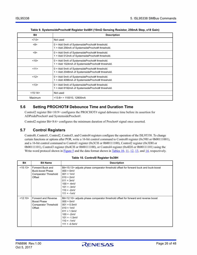
5.6 Setting PROCHOT# Debounce Time and Duration TimeControl2 register Bit<10:9> configures the PROCHOT# signal debounce time before its assertion for ADPsideProchot# and SystemsideProchot#.
Control2 register Bit<8:6> configures the minimum duration of Prochot# signal once asserted.
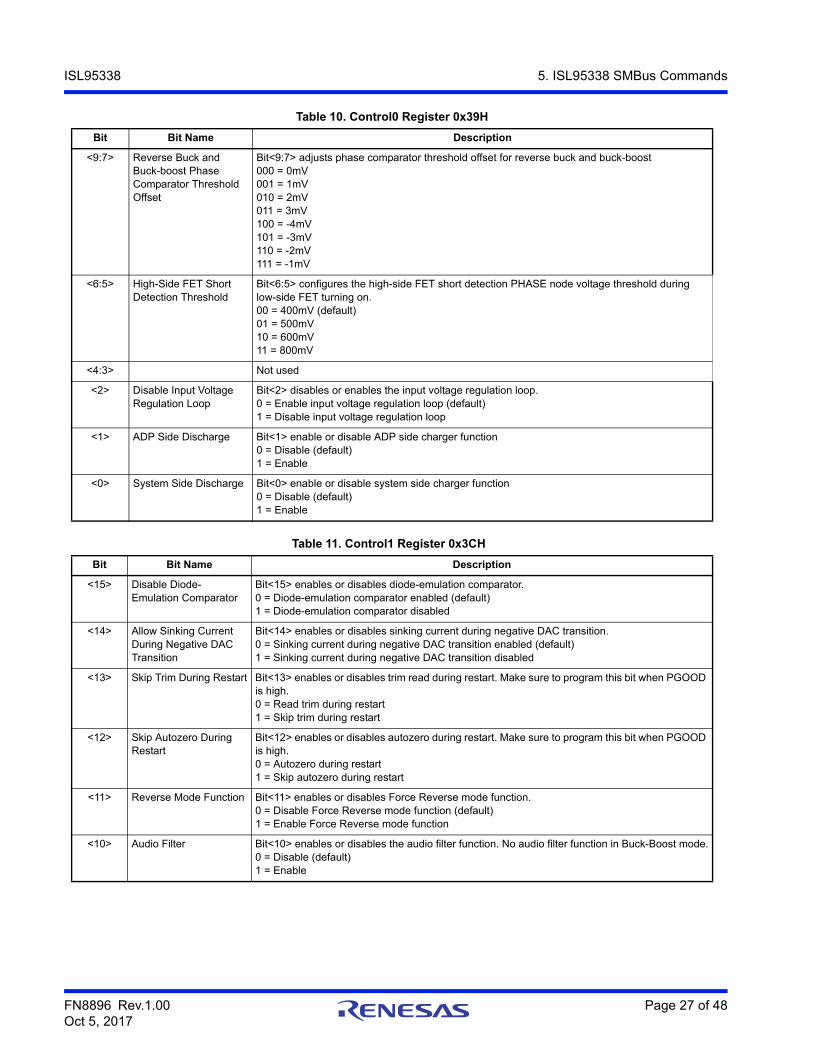
5.7 Control RegistersControl0, Control1, Control2, Control3, and Control4 registers configure the operation of the ISL95338. To change certain functions or options after POR, write a 16-bit control command to Control0 register (0x39H or 0b00111001), and a 16-bit control command to Control1 register (0x3CH or 0b00111100), Control2 register (0x3DH or 0b00111101), Control3 register (0x4CH or 0b00111100), or Control4 register (0x4EH or 0b00111101) using the Write-word protocol shown in Figure 5 and the data format shown in Tables 10, 11, 12, 13, and 14, respectively.
Table 9. SystemsideProchot# Register 0x48H (10mΩ Sensing Resistor, 256mA Step, x18 Gain)
Bit Description
<7:0> Not used
<8> 0 = Add 0mA of SystemsideProchot# threshold. 1 = Add 256mA of SystemsideProchot# threshold.
<9> 0 = Add 0mA of SystemsideProchot# threshold. 1 = Add 512mA of SystemsideProchot# threshold.
<10> 0 = Add 0mA of SystemsideProchot# threshold. 1 = Add 1024mA of SystemsideProchot# threshold.
<11> 0 = Add 0mA of SystemsideProchot# threshold. 1 = Add 2048mA of SystemsideProchot# threshold.
<12> 0 = Add 0mA of SystemsideProchot# threshold. 1 = Add 4096mA of SystemsideProchot# threshold.
<13> 0 = Add 0mA of SystemsideProchot# threshold. 1 = Add 8192mA of SystemsideProchot# threshold.
<15:14> Not used
Maximum <13:8> = 110010, 12800mA
Table 10. Control0 Register 0x39H
Bit Bit Name Description
<15:13> Forward Buck and Buck-boost Phase Comparator Threshold Offset
Bit<15:13> adjusts phase comparator threshold offset for forward buck and buck-boost000 = 0mV001 = 1mV010 = 2mV011 = 3mV100 = -4mV101 = -3mV110 = -2mV111 = -1mV
<12:10> Forward and Reverse Boost Phase Comparator Threshold Offset
Bit<12:10> adjusts phase comparator threshold offset for forward and reverse boost000 = 0mV001 = 0.5mV010 = 1mV011 = 1.5mV100 = -2mV101 = -1.5mV110 = -1mV111 = -0.5mV
FN8896 Rev.1.00 Page 27 of 48Oct 5, 2017
ISL95338 5. ISL95338 SMBus Commands
<9:7> Reverse Buck and Buck-boost Phase Comparator Threshold Offset
Bit<9:7> adjusts phase comparator threshold offset for reverse buck and buck-boost000 = 0mV001 = 1mV010 = 2mV011 = 3mV100 = -4mV101 = -3mV110 = -2mV111 = -1mV
<6:5> High-Side FET Short Detection Threshold
Bit<6:5> configures the high-side FET short detection PHASE node voltage threshold during low-side FET turning on.00 = 400mV (default)01 = 500mV10 = 600mV11 = 800mV
<4:3> Not used
<2> Disable Input Voltage Regulation Loop
Bit<2> disables or enables the input voltage regulation loop.0 = Enable input voltage regulation loop (default)1 = Disable input voltage regulation loop
<1> ADP Side Discharge Bit<1> enable or disable ADP side charger function0 = Disable (default)1 = Enable
<0> System Side Discharge Bit<0> enable or disable system side charger function0 = Disable (default)1 = Enable
Table 11. Control1 Register 0x3CH
Bit Bit Name Description
<15> Disable Diode-Emulation Comparator
Bit<15> enables or disables diode-emulation comparator.0 = Diode-emulation comparator enabled (default)1 = Diode-emulation comparator disabled
<14> Allow Sinking Current During Negative DAC Transition
Bit<14> enables or disables sinking current during negative DAC transition.0 = Sinking current during negative DAC transition enabled (default)1 = Sinking current during negative DAC transition disabled
<13> Skip Trim During Restart Bit<13> enables or disables trim read during restart. Make sure to program this bit when PGOOD is high.0 = Read trim during restart1 = Skip trim during restart
<12> Skip Autozero During Restart
Bit<12> enables or disables autozero during restart. Make sure to program this bit when PGOOD is high.0 = Autozero during restart1 = Skip autozero during restart
<11> Reverse Mode Function Bit<11> enables or disables Force Reverse mode function.0 = Disable Force Reverse mode function (default)1 = Enable Force Reverse mode function
<10> Audio Filter Bit<10> enables or disables the audio filter function. No audio filter function in Buck-Boost mode.0 = Disable (default)1 = Enable
Table 10. Control0 Register 0x39H
Bit Bit Name Description
FN8896 Rev.1.00 Page 28 of 48Oct 5, 2017
ISL95338 5. ISL95338 SMBus Commands
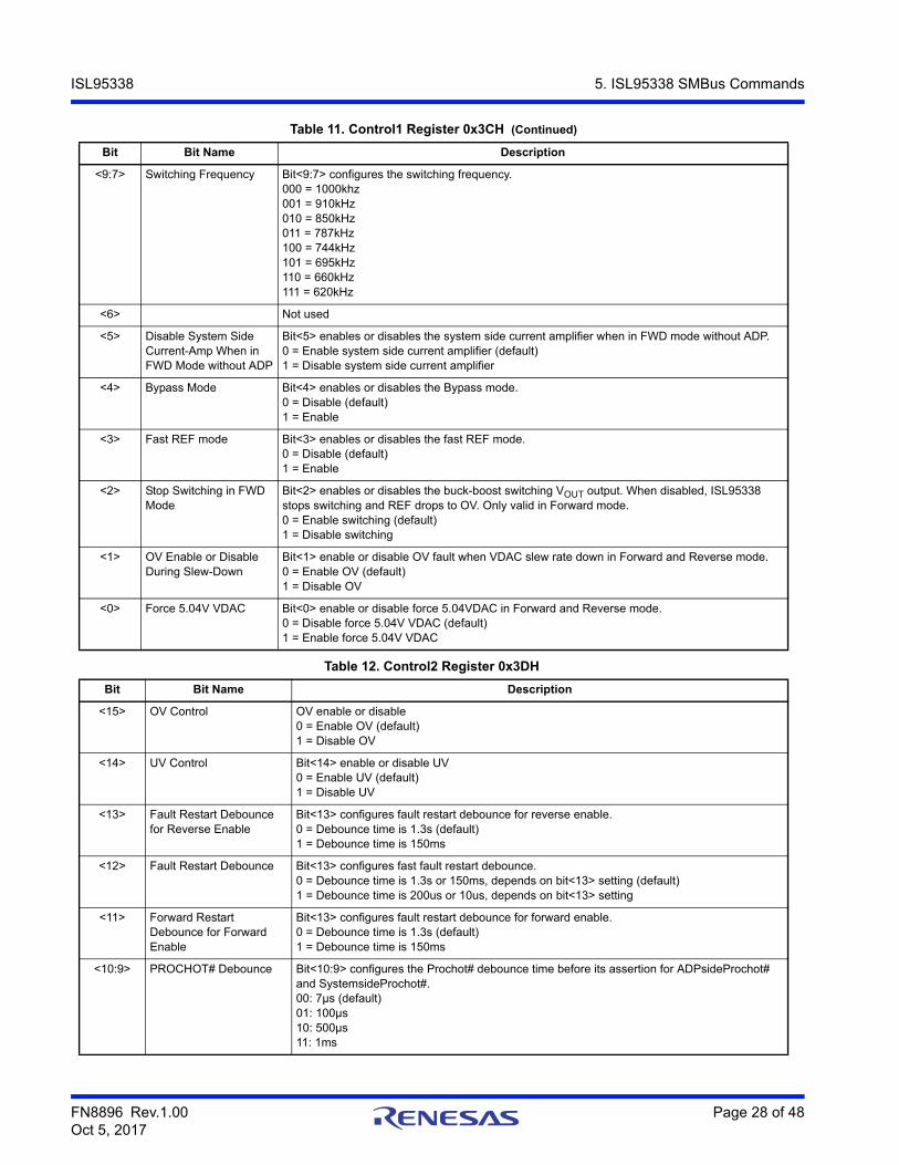
<9:7> Switching Frequency Bit<9:7> configures the switching frequency.000 = 1000khz001 = 910kHz010 = 850kHz011 = 787kHz100 = 744kHz101 = 695kHz110 = 660kHz111 = 620kHz
<6> Not used
<5> Disable System Side Current-Amp When in FWD Mode without ADP
Bit<5> enables or disables the system side current amplifier when in FWD mode without ADP.0 = Enable system side current amplifier (default)1 = Disable system side current amplifier
<4> Bypass Mode Bit<4> enables or disables the Bypass mode.0 = Disable (default)1 = Enable
<3> Fast REF mode Bit<3> enables or disables the fast REF mode.0 = Disable (default)1 = Enable
<2> Stop Switching in FWD Mode
Bit<2> enables or disables the buck-boost switching VOUT output. When disabled, ISL95338 stops switching and REF drops to OV. Only valid in Forward mode.0 = Enable switching (default)1 = Disable switching
<1> OV Enable or Disable During Slew-Down
Bit<1> enable or disable OV fault when VDAC slew rate down in Forward and Reverse mode.0 = Enable OV (default)1 = Disable OV
<0> Force 5.04V VDAC Bit<0> enable or disable force 5.04VDAC in Forward and Reverse mode.0 = Disable force 5.04V VDAC (default)1 = Enable force 5.04V VDAC
Table 12. Control2 Register 0x3DH
Bit Bit Name Description
<15> OV Control OV enable or disable0 = Enable OV (default)1 = Disable OV
<14> UV Control Bit<14> enable or disable UV0 = Enable UV (default)1 = Disable UV
<13> Fault Restart Debounce for Reverse Enable
Bit<13> configures fault restart debounce for reverse enable.0 = Debounce time is 1.3s (default)1 = Debounce time is 150ms
<12> Fault Restart Debounce Bit<13> configures fast fault restart debounce.0 = Debounce time is 1.3s or 150ms, depends on bit<13> setting (default)1 = Debounce time is 200us or 10us, depends on bit<13> setting
<11> Forward Restart Debounce for Forward Enable
Bit<13> configures fault restart debounce for forward enable.0 = Debounce time is 1.3s (default)1 = Debounce time is 150ms
<10:9> PROCHOT# Debounce Bit<10:9> configures the Prochot# debounce time before its assertion for ADPsideProchot# and SystemsideProchot#.00: 7µs (default)01: 100µs 10: 500µs11: 1ms
Table 11. Control1 Register 0x3CH (Continued)
Bit Bit Name Description
FN8896 Rev.1.00 Page 29 of 48Oct 5, 2017
ISL95338 5. ISL95338 SMBus Commands
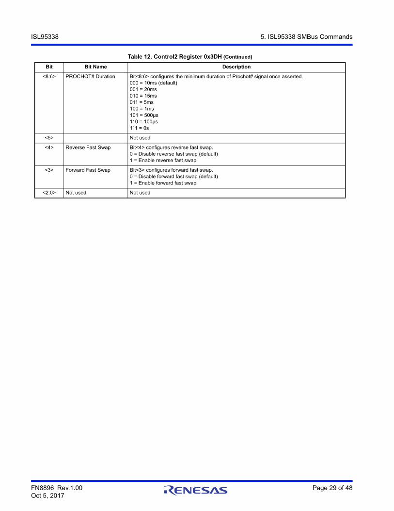
<8:6> PROCHOT# Duration Bit<8:6> configures the minimum duration of Prochot# signal once asserted.000 = 10ms (default)001 = 20ms010 = 15ms011 = 5ms100 = 1ms101 = 500µs110 = 100µs111 = 0s
<5> Not used
<4> Reverse Fast Swap Bit<4> configures reverse fast swap.0 = Disable reverse fast swap (default)1 = Enable reverse fast swap
<3> Forward Fast Swap Bit<3> configures forward fast swap.0 = Disable forward fast swap (default)1 = Enable forward fast swap
<2:0> Not used Not used
Table 12. Control2 Register 0x3DH (Continued)
Bit Bit Name Description
FN8896 Rev.1.00 Page 30 of 48Oct 5, 2017
ISL95338 5. ISL95338 SMBus Commands
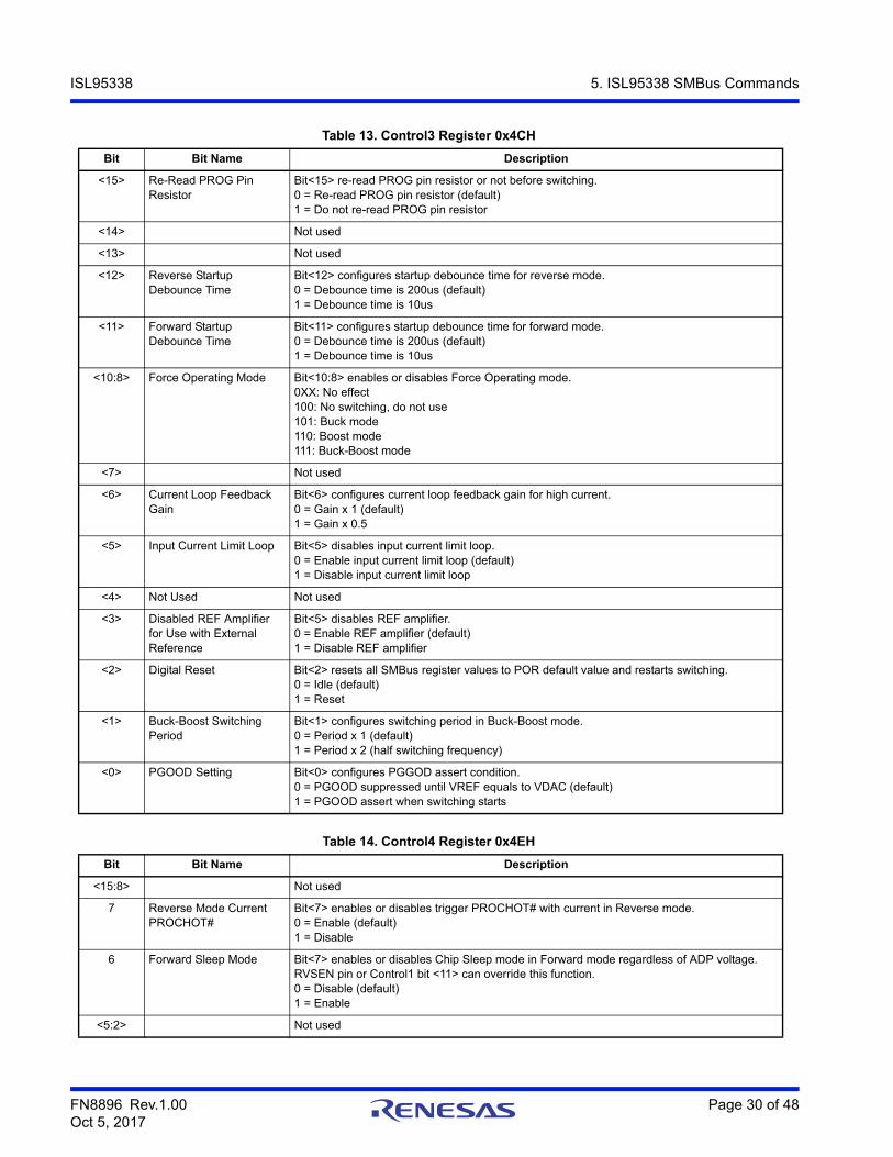
Table 13. Control3 Register 0x4CH
Bit Bit Name Description
<15> Re-Read PROG Pin Resistor
Bit<15> re-read PROG pin resistor or not before switching.0 = Re-read PROG pin resistor (default)1 = Do not re-read PROG pin resistor
<14> Not used
<13> Not used
<12> Reverse Startup Debounce Time
Bit<12> configures startup debounce time for reverse mode.0 = Debounce time is 200us (default)1 = Debounce time is 10us
<11> Forward Startup Debounce Time
Bit<11> configures startup debounce time for forward mode.0 = Debounce time is 200us (default)1 = Debounce time is 10us
<10:8> Force Operating Mode Bit<10:8> enables or disables Force Operating mode.0XX: No effect100: No switching, do not use101: Buck mode110: Boost mode111: Buck-Boost mode
<7> Not used
<6> Current Loop Feedback Gain
Bit<6> configures current loop feedback gain for high current.0 = Gain x 1 (default)1 = Gain x 0.5
<5> Input Current Limit Loop Bit<5> disables input current limit loop.0 = Enable input current limit loop (default)1 = Disable input current limit loop
<4> Not Used Not used
<3> Disabled REF Amplifier for Use with External Reference
Bit<5> disables REF amplifier.0 = Enable REF amplifier (default)1 = Disable REF amplifier
<2> Digital Reset Bit<2> resets all SMBus register values to POR default value and restarts switching.0 = Idle (default)1 = Reset
<1> Buck-Boost Switching Period
Bit<1> configures switching period in Buck-Boost mode.0 = Period x 1 (default)1 = Period x 2 (half switching frequency)
<0> PGOOD Setting Bit<0> configures PGGOD assert condition.0 = PGOOD suppressed until VREF equals to VDAC (default)1 = PGOOD assert when switching starts
Table 14. Control4 Register 0x4EH
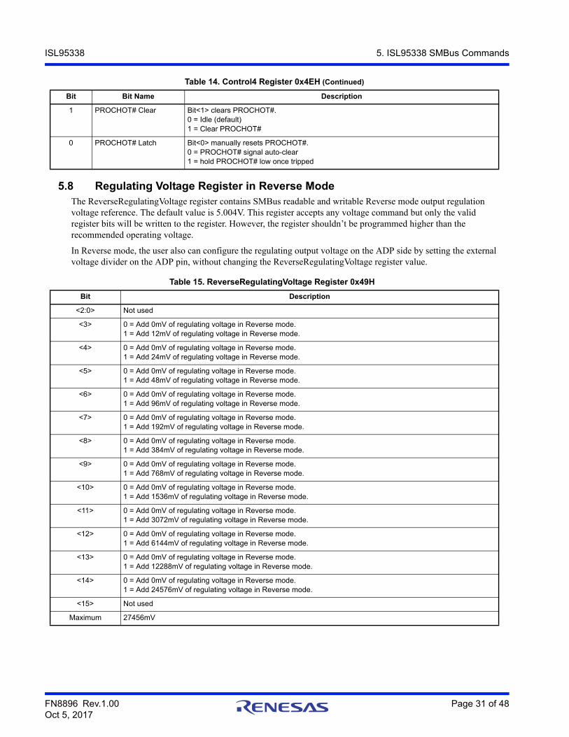
Bit Bit Name Description
<15:8> Not used
7 Reverse Mode Current PROCHOT#
Bit<7> enables or disables trigger PROCHOT# with current in Reverse mode.0 = Enable (default)1 = Disable
6 Forward Sleep Mode Bit<7> enables or disables Chip Sleep mode in Forward mode regardless of ADP voltage. RVSEN pin or Control1 bit <11> can override this function.0 = Disable (default)1 = Enable
<5:2> Not used
FN8896 Rev.1.00 Page 31 of 48Oct 5, 2017
ISL95338 5. ISL95338 SMBus Commands
5.8 Regulating Voltage Register in Reverse ModeThe ReverseRegulatingVoltage register contains SMBus readable and writable Reverse mode output regulation voltage reference. The default value is 5.004V. This register accepts any voltage command but only the valid register bits will be written to the register. However, the register shouldn’t be programmed higher than the recommended operating voltage.
In Reverse mode, the user also can configure the regulating output voltage on the ADP side by setting the external voltage divider on the ADP pin, without changing the ReverseRegulatingVoltage register value.
1 PROCHOT# Clear Bit<1> clears PROCHOT#.0 = Idle (default)1 = Clear PROCHOT#
0 PROCHOT# Latch Bit<0> manually resets PROCHOT#.0 = PROCHOT# signal auto-clear1 = hold PROCHOT# low once tripped
Table 15. ReverseRegulatingVoltage Register 0x49H
Bit Description
<2:0> Not used
<3> 0 = Add 0mV of regulating voltage in Reverse mode.1 = Add 12mV of regulating voltage in Reverse mode.
<4> 0 = Add 0mV of regulating voltage in Reverse mode.1 = Add 24mV of regulating voltage in Reverse mode.
<5> 0 = Add 0mV of regulating voltage in Reverse mode.1 = Add 48mV of regulating voltage in Reverse mode.
<6> 0 = Add 0mV of regulating voltage in Reverse mode.1 = Add 96mV of regulating voltage in Reverse mode.
<7> 0 = Add 0mV of regulating voltage in Reverse mode.1 = Add 192mV of regulating voltage in Reverse mode.
<8> 0 = Add 0mV of regulating voltage in Reverse mode.1 = Add 384mV of regulating voltage in Reverse mode.
<9> 0 = Add 0mV of regulating voltage in Reverse mode.1 = Add 768mV of regulating voltage in Reverse mode.
<10> 0 = Add 0mV of regulating voltage in Reverse mode.1 = Add 1536mV of regulating voltage in Reverse mode.
<11> 0 = Add 0mV of regulating voltage in Reverse mode.1 = Add 3072mV of regulating voltage in Reverse mode.
<12> 0 = Add 0mV of regulating voltage in Reverse mode.1 = Add 6144mV of regulating voltage in Reverse mode.
<13> 0 = Add 0mV of regulating voltage in Reverse mode.1 = Add 12288mV of regulating voltage in Reverse mode.
<14> 0 = Add 0mV of regulating voltage in Reverse mode.1 = Add 24576mV of regulating voltage in Reverse mode.
<15> Not used
Maximum 27456mV
Table 14. Control4 Register 0x4EH (Continued)
Bit Bit Name Description
FN8896 Rev.1.00 Page 32 of 48Oct 5, 2017
ISL95338 5. ISL95338 SMBus Commands
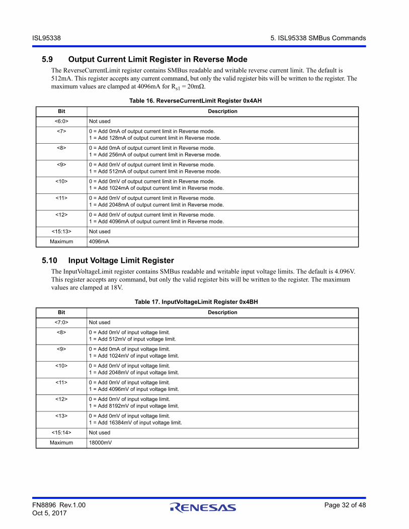
5.9 Output Current Limit Register in Reverse ModeThe ReverseCurrentLimit register contains SMBus readable and writable reverse current limit. The default is 512mA. This register accepts any current command, but only the valid register bits will be written to the register. The maximum values are clamped at 4096mA for Rs1 = 20mΩ.
5.10 Input Voltage Limit RegisterThe InputVoltageLimit register contains SMBus readable and writable input voltage limits. The default is 4.096V. This register accepts any command, but only the valid register bits will be written to the register. The maximum values are clamped at 18V.
Table 16. ReverseCurrentLimit Register 0x4AH
Bit Description
<6:0> Not used
<7> 0 = Add 0mA of output current limit in Reverse mode.1 = Add 128mA of output current limit in Reverse mode.
<8> 0 = Add 0mA of output current limit in Reverse mode.1 = Add 256mA of output current limit in Reverse mode.
<9> 0 = Add 0mV of output current limit in Reverse mode.1 = Add 512mA of output current limit in Reverse mode.
<10> 0 = Add 0mV of output current limit in Reverse mode.1 = Add 1024mA of output current limit in Reverse mode.
<11> 0 = Add 0mV of output current limit in Reverse mode.1 = Add 2048mA of output current limit in Reverse mode.
<12> 0 = Add 0mV of output current limit in Reverse mode.1 = Add 4096mA of output current limit in Reverse mode.
<15:13> Not used
Maximum 4096mA
Table 17. InputVoltageLimit Register 0x4BH
Bit Description
<7:0> Not used
<8> 0 = Add 0mV of input voltage limit.1 = Add 512mV of input voltage limit.
<9> 0 = Add 0mA of input voltage limit.1 = Add 1024mV of input voltage limit.
<10> 0 = Add 0mV of input voltage limit.1 = Add 2048mV of input voltage limit.
<11> 0 = Add 0mV of input voltage limit.1 = Add 4096mV of input voltage limit.
<12> 0 = Add 0mV of input voltage limit.1 = Add 8192mV of input voltage limit.
<13> 0 = Add 0mV of input voltage limit.1 = Add 16384mV of input voltage limit.
<15:14> Not used
Maximum 18000mV
FN8896 Rev.1.00 Page 33 of 48Oct 5, 2017
ISL95338 5. ISL95338 SMBus Commands
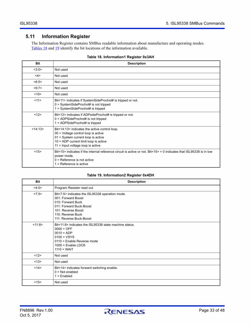
5.11 Information RegisterThe Information Register contains SMBus readable information about manufacture and operating modes. Tables 18 and 19 identify the bit locations of the information available.
Table 18. Information1 Register 0x3AH
Bit Description
<3:0> Not used
<4> Not used
<6:5> Not used
<9:7> Not used
<10> Not used
<11> Bit<11> indicates if SystemSideProchot# is tripped or not.0 = SystemSideProchot# is not tripped1 = SystemSideProchot# is tripped
<12> Bit<12> indicates if ADPsideProchot# is tripped or not.0 = ADPSideProchot# is not tripped1 = ADPSideProchot# is tripped
<14:13> Bit<14:13> indicates the active control loop.00 = Voltage control loop is active01 = System current loop is active10 = ADP current limit loop is active11 = Input voltage loop is active
<15> Bit<15> indicates if the internal reference circuit is active or not. Bit<15> = 0 indicates that ISL95338 is in low power mode.0 = Reference is not active1 = Reference is active
Table 19. Information2 Register 0x4DH
Bit Description
<4:0> Program Resister read out
<7:5> Bit<7:5> indicates the ISL95338 operation mode.001: Forward Boost010: Forward Buck011: Forward Buck-Boost101: Reverse Boost110: Reverse Buck111: Reverse Buck-Boost
<11:8> Bit<11:8> indicates the ISL95338 state machine status.0000 = OFF0010 = ADP0100 = VSYS0110 = Enable Reverse mode1000 = Enable LDO51110 = WAIT
<12> Not used
<13> Not used
<14> Bit<14> indicates forward switching enable.0 = Not enabled1 = Enabled
<15> Not used
FN8896 Rev.1.00 Page 34 of 48Oct 5, 2017
ISL95338 6. Application Information
6. Application Information
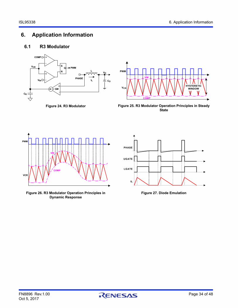
6.1 R3 Modulator
Figure 24. R3 Modulator Figure 25. R3 Modulator Operation Principles in Steady State
Figure 26. R3 Modulator Operation Principles in Dynamic Response
Figure 27. Diode Emulation
COMP
R
IL
GM
PHASE
CR
VW
SQ PWM
L
CO
VO
VCR
+
+
+
-
-
-
COMP
PWM
VCRHYSTERETIC
WINDOW
VW
PWM
VCR
VW
COMP
UGATE
PHASE
IL
LGATE
FN8896 Rev.1.00 Page 35 of 48Oct 5, 2017
ISL95338 6. Application Information
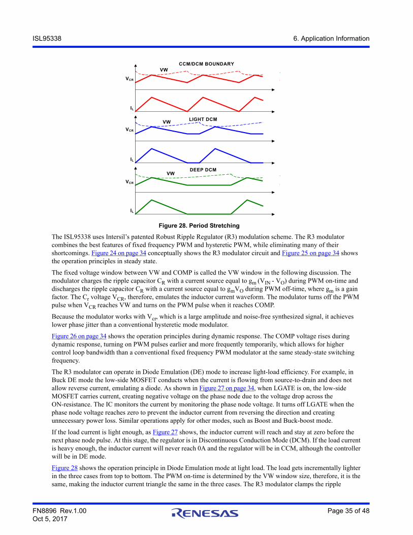
Figure 28. Period Stretching
The ISL95338 uses Intersil’s patented Robust Ripple Regulator (R3) modulation scheme. The R3 modulator combines the best features of fixed frequency PWM and hysteretic PWM, while eliminating many of their shortcomings. Figure 24 on page 34 conceptually shows the R3 modulator circuit and Figure 25 on page 34 shows the operation principles in steady state.
The fixed voltage window between VW and COMP is called the VW window in the following discussion. The modulator charges the ripple capacitor CR with a current source equal to gm (VIN - VO) during PWM on-time and discharges the ripple capacitor CR with a current source equal to gmVO during PWM off-time, where gm is a gain factor. The Cr voltage VCR, therefore, emulates the inductor current waveform. The modulator turns off the PWM pulse when VCR reaches VW and turns on the PWM pulse when it reaches COMP.
Because the modulator works with Vcr, which is a large amplitude and noise-free synthesized signal, it achieves lower phase jitter than a conventional hysteretic mode modulator.
Figure 26 on page 34 shows the operation principles during dynamic response. The COMP voltage rises during dynamic response, turning on PWM pulses earlier and more frequently temporarily, which allows for higher control loop bandwidth than a conventional fixed frequency PWM modulator at the same steady-state switching frequency.
The R3 modulator can operate in Diode Emulation (DE) mode to increase light-load efficiency. For example, in Buck DE mode the low-side MOSFET conducts when the current is flowing from source-to-drain and does not allow reverse current, emulating a diode. As shown in Figure 27 on page 34, when LGATE is on, the low-side MOSFET carries current, creating negative voltage on the phase node due to the voltage drop across the ON-resistance. The IC monitors the current by monitoring the phase node voltage. It turns off LGATE when the phase node voltage reaches zero to prevent the inductor current from reversing the direction and creating unnecessary power loss. Similar operations apply for other modes, such as Boost and Buck-boost mode.
If the load current is light enough, as Figure 27 shows, the inductor current will reach and stay at zero before the next phase node pulse. At this stage, the regulator is in Discontinuous Conduction Mode (DCM). If the load current is heavy enough, the inductor current will never reach 0A and the regulator will be in CCM, although the controller will be in DE mode.
Figure 28 shows the operation principle in Diode Emulation mode at light load. The load gets incrementally lighter in the three cases from top to bottom. The PWM on-time is determined by the VW window size, therefore, it is the same, making the inductor current triangle the same in the three cases. The R3 modulator clamps the ripple
IL
IL
VCR
IL
VCR
VCR
VWCCM/DCM BOUNDARY
LIGHT DCM
DEEP DCM
VW
VW
FN8896 Rev.1.00 Page 36 of 48Oct 5, 2017
ISL95338 6. Application Information
capacitor voltage VCR in DE mode to make it mimic the inductor current. It takes the COMP voltage longer to hit VCR, naturally stretching the switching period. The inductor current triangles move further apart from each other, such that the inductor current average value is equal to the load current. The reduced switching frequency helps increase light-load efficiency.
6.2 ISL95338 Bidirectional Buck-Boost Voltage RegulatorThe ISL95338 bidirectional buck-boost voltage regulator drives an external N-channel MOSFET bridge comprised of two transistor pairs as shown in Figure 2. The first pair, Q1 and Q2, is a buck arrangement with the transistor center tap connected to an inductor “input”, as is the case with a buck converter in Forward mode. The second transistor pair, Q3 and Q4, is a boost arrangement with the transistor center tap connected to the same inductor’s “output”, as is the case with a boost converter in Forward mode. This arrangement supports the same operation mode in reverse direction.
• In Forward Buck mode, Q1 and Q2 turn on and off alternatively, while Q3 remains off and Q4 remains on.
• In Forward Boost mode, Q3 and Q4 turn on and off alternatively, while Q1 remains on and Q2 remains off.
• In Forward Buck-Boost mode, Q1 and Q3 turn on at the same time, Q3 turns off and Q4 turns on, Q1 turns off and Q2 turns on, and after Q2 and Q4 turn off at the same time, and Q1 and Q3 turn on again.
• In Forward Bypass mode, Q1 and Q4 are always on, while Q2 and Q3 are always off.
• In Reverse Buck mode, Q3 and Q4 turn on and off alternatively, while Q2 remains off and Q1 remains on.
• In Reverse Boost mode, Q1 and Q2 turn on and off alternatively, while Q4 remains on and Q3 remains off.
• In Reverse Buck-Boost mode, Q4 and Q2 turn on at the same time, Q2 turns off and Q1 turns on, Q4 turns off and Q3 turns on, and after Q3 and Q1 turn off at the same time and Q4 and Q2 turn on again.
• In Reverse Bypass mode, Q1 and Q4 are always on, except during the needed refresh time, while Q2 and Q3 are always off.
• In Reverse mode the output sensing point is CSIP pin.
Figure 29. Buck-Boost Regulator Topology
Table 20. Operation Mode
Mode Q1 Q2 Q3 Q4
Forward Buck Control FET Sync. FET OFF ON
Forward Boost ON OFF Control FET Sync. FET
Forward Buck-Boost Control FET Sync. FET Control FET Sync. FET
Forward Bypass ON OFF OFF ON
Reverse Buck ON OFF Sync. FET Control FET
Reverse Boost Sync. FET Control FET OFF ON
Reverse Buck-Boost Sync. FET Control FET Sync. FET Control FET
Reverse Bypass ON OFF OFF ON
FN8896 Rev.1.00 Page 37 of 48Oct 5, 2017
ISL95338 6. Application Information
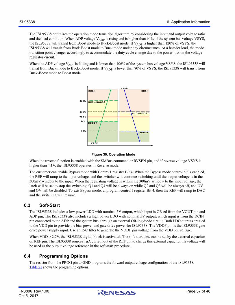
The ISL95338 optimizes the operation mode transition algorithm by considering the input and output voltage ratio and the load condition. When ADP voltage VADP is rising and is higher than 94% of the system bus voltage VSYS, the ISL95338 will transit from Boost mode to Buck-Boost mode. If VADP is higher than 120% of VSYS, the ISL95338 will transit from Buck-Boost mode to Buck mode under any circumstance. At a heavier load, the mode transition point changes accordingly to accommodate the duty cycle change due to the power loss on the voltage regulator circuit.
When the ADP voltage VADP is falling and is lower than 106% of the system bus voltage VSYS, the ISL95338 will transit from Buck mode to Buck-Boost mode. If VADP is lower than 80% of VSYS, the ISL95338 will transit from Buck-Boost mode to Boost mode.
Figure 30. Operation Mode
When the reverse function is enabled with the SMBus command or RVSEN pin, and if reverse voltage VSYS is higher than 4.1V, the ISL95338 operates in Reverse mode.
The customer can enable Bypass mode with Control1 register Bit 4. When the Bypass mode control bit is enabled, the REF will ramp to the input voltage, and the switcher will continue switching until the output voltage is in the 300mV window to the input. When the regulating voltage is within the 300mV window to the input voltage, the latch will be set to stop the switching, Q1 and Q4 will be always on while Q2 and Q3 will be always off, and UV and OV will be disabled. To exit Bypass mode, unprogram control1 register Bit 4, then the REF will ramp to DAC and the switching will resume.
6.3 Soft-StartThe ISL95338 includes a low power LDO with nominal 5V output, which input is OR-ed from the VOUT pin and ADP pin. The ISL95338 also includes a high power LDO with nominal 5V output, which input is from the DCIN pin connected to the ADP and the system bus, through an external OR-ing diode circuit. Both LDO outputs are tied to the VDD pin to provide the bias power and gate drive power for ISL95338. The VDDP pin is the ISL95338 gate drive power supply input. Use an R-C filter to generate the VDDP pin voltage from the VDD pin voltage.
When VDD > 2.7V, the ISL95338 digital block is activated. The soft-start time can be set by the external capacitor on REF pin. The ISL95338 sources 1µA current out of the REF pin to charge this external capacitor. Its voltage will be used as the output voltage reference in the soft-start procedure.
6.4 Programming OptionsThe resistor from the PROG pin to GND programs the forward output voltage configuration of the ISL95338. Table 21 shows the programing options.
94%
120%
106%
80%
VSYS
VA DP
VA DP
BU CK-BO O ST
BUCK
B O O ST
BO O ST
B UCK-BO O ST
BUCK
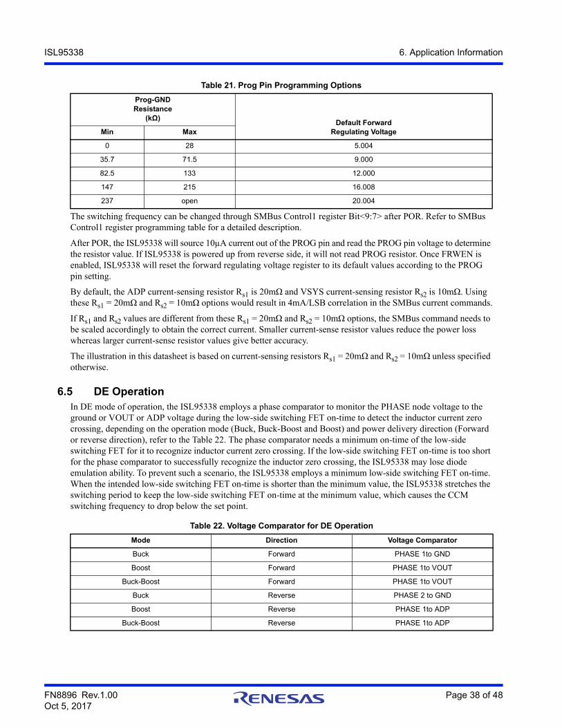
FN8896 Rev.1.00 Page 38 of 48Oct 5, 2017
ISL95338 6. Application Information
The switching frequency can be changed through SMBus Control1 register Bit<9:7> after POR. Refer to SMBus Control1 register programming table for a detailed description.
After POR, the ISL95338 will source 10µA current out of the PROG pin and read the PROG pin voltage to determine the resistor value. If ISL95338 is powered up from reverse side, it will not read PROG resistor. Once FRWEN is enabled, ISL95338 will reset the forward regulating voltage register to its default values according to the PROG pin setting.
By default, the ADP current-sensing resistor Rs1 is 20mΩ and VSYS current-sensing resistor Rs2 is 10mΩ. Using these Rs1 = 20mΩand Rs2 = 10mΩ options would result in 4mA/LSB correlation in the SMBus current commands.
If Rs1 and Rs2 values are different from these Rs1 = 20mΩand Rs2 = 10mΩ options, the SMBus command needs to be scaled accordingly to obtain the correct current. Smaller current-sense resistor values reduce the power loss whereas larger current-sense resistor values give better accuracy.
The illustration in this datasheet is based on current-sensing resistors Rs1 = 20mΩ and Rs2 = 10mΩ unless specified otherwise.
6.5 DE OperationIn DE mode of operation, the ISL95338 employs a phase comparator to monitor the PHASE node voltage to the ground or VOUT or ADP voltage during the low-side switching FET on-time to detect the inductor current zero crossing, depending on the operation mode (Buck, Buck-Boost and Boost) and power delivery direction (Forward or reverse direction), refer to the Table 22. The phase comparator needs a minimum on-time of the low-side switching FET for it to recognize inductor current zero crossing. If the low-side switching FET on-time is too short for the phase comparator to successfully recognize the inductor zero crossing, the ISL95338 may lose diode emulation ability. To prevent such a scenario, the ISL95338 employs a minimum low-side switching FET on-time. When the intended low-side switching FET on-time is shorter than the minimum value, the ISL95338 stretches the switching period to keep the low-side switching FET on-time at the minimum value, which causes the CCM switching frequency to drop below the set point.
Table 21. Prog Pin Programming Options
Prog-GNDResistance
(kΩ)Default Forward
Regulating VoltageMin Max
0 28 5.004
35.7 71.5 9.000
82.5 133 12.000
147 215 16.008
237 open 20.004
Table 22. Voltage Comparator for DE Operation
Mode Direction Voltage Comparator
Buck Forward PHASE 1to GND
Boost Forward PHASE 1to VOUT
Buck-Boost Forward PHASE 1to VOUT
Buck Reverse PHASE 2 to GND
Boost Reverse PHASE 1to ADP
Buck-Boost Reverse PHASE 1to ADP
FN8896 Rev.1.00 Page 39 of 48Oct 5, 2017
ISL95338 6. Application Information
6.6 Forward ModeWhen the forward function is enabled with the SMBus command or FRWEN pin (voltage is higher than 0.8V) and DCIN is powered by ADP, and if the ADP is plugged in and its value is higher than 4.1V, the ISL95338 can operate in Forward Buck mode, Forward Boost mode, Forward Buck-Boost mode, or Forward Bypass mode. After the forward output voltage reaches the regulating output voltage range set by register 0X15H Bit<14:3>, forward power-good FWGPG will assert to High.
6.7 Reverse Mode for USB OTG (On-the-Go)When the reverse function is enabled with the SMBus command (Control1 Bit 11) or RVSEN pin, and if an external voltage is on system side and its value is higher than 4.1V, the ISL95338 can operate in Reverse Buck mode, Reverse Boost mode, Reverse Buck-Boost mode, or Reverse Bypass mode. RVSEN is the digital input pin. The 1.3s or 150ms debounce time can be set by Control2 register Bit<13>. After the reverse output voltage reaches the output voltage set by register 0X49H Bit<14:3>, reverse power-good RVSPG will assert to High.
Before Reverse mode starts switching, the CSIP pin voltage needs to drop below the reverse output overvoltage protection threshold (ReverseRegulatingVoltage + 1177mV) first.
The default reverse output voltage is 5V and programmable up to 20V in Reverse Buck, Reverse Buck-Boost, and Reverse Boost mode. In Reverse Bypass mode, the maximum value of reverse output voltage is programmable up to 20V. The reverse voltage register 0X49H can be used to configure the reverse output voltage.
6.8 Fast REFTo achieve fast REF in some applications, the fast REF function can be programmed by Control1 Bit3. If this bit is programmed, 1uA current source for REF pin will be replaced with 5k impedance to get faster transitions for REF voltage.
6.9 Fast SwapThe ISL95338 provides fast swap function in Forward mode and Reverse mode. Users can implement the fast swap function in Forward mode in one of two ways (pin reverse or software reverse) by following the steps below:
• Pin reverse fast swap enable:
(1) Program Control2 Bit4 (Reverse Fast Swap).(2) Skip trim during restart by programming control1 Bit 13.(3) Skip autozero during restart by programming control1 Bit 12.(4) Enable RVSEN pin.
• Software reverse fast swap enable:
(1) Program Control1 Bit0 (Force 5.04V VDAC).(2) Program Control1 Bit3 (Fast REF).(3) Skip trim during restart with programming control1 Bit 13.(4) Skip autozero during restart with programming control1 Bit 12.(5) Program Control1 Bit11 (Force Reverse mode).Similarly, users can implement the fast swap function in Reverse mode in one of two ways (pin reverse or software reverse) by following the steps below:
• Pin forward fast swap enable:
(1) Program Control2 Bit3 (Forward Fast Swap).(2) Skip trim during restart by programming control1 Bit 13.(3) Skip autozero during restart by programming control1 Bit 12.(4) Disable RVSEN pin.(5) Enable FWREN pin.
• Software forward fast swap enable:
FN8896 Rev.1.00 Page 40 of 48Oct 5, 2017
ISL95338 6. Application Information
(1) Program Control1 Bit0 (Force 5.04V VDAC).(2) Program Control1 Bit3 (Fast REF).(3) Skip trim during restart by programming control1 Bit 13.(4) Skip autozero during restart by programming control1 Bit 12.(5) Un-program Control1 Bit11 (Force Reverse mode).
6.10 ADP Input Overvoltage ProtectionIf the ADP pin input voltage exceeds 26.4V for more than 10µs, the ISL95338 will declare an ADP overvoltage condition and stop switching. When the ADP voltage drops below 25.608V for more than 100µs, the ISL95338 will start to switch.
6.11 System Output Overvoltage ProtectionThe ISL95338 provides system rail output overvoltage protection. If the system voltage VOUTS is 1095mV higher than the ForwardRegulatingVoltage register set value for more than 100us, it will declare the system overvoltage, de-assert FWRPG, and stop switching. It will resume switching with the 100us debounce when VOUTS is less than 542mV plus the setting reference voltage for forward.
6.12 System Output Undervoltage ProtectionThe ISL95338 provides system rail output undervoltage protection. If the system voltage VOUTS is 818mV lower than the ForwardRegulatingVoltage register set value for more than 1ms, it will declare the system undervoltage, de-assert FWRPG, and restart.
6.13 ADP Output Overvoltage ProtectionThe ISL95338 provides ADP rail output overvoltage protection. If the ADP voltage ADPS is 1177mV higher than the ReverseRegulatingVoltage register set value for more than 100us, it will declare the ADP overvoltage, de-assert RVSPG, and stop switching. The ISL95338 will resume switching with the 100us debounce when ADPS is less than 583mV plus the setting reference voltage for reverse.
6.14 ADP Output Undervoltage ProtectionThe ISL95338 provides ADP rail output undervoltage protection. If the ADP voltage VADPS is 1177mV lower than the ReverseRegulatingVoltage register set value for more than 1ms, it will declare the ADP undervoltage, de-assert RVSPG, and stop switching.
6.15 Over-Temperature ProtectionThe ISL95338 will stop switching for self protection when the junction temperature exceeds +140°C.
When the temperature falls below +120°C, and after a 100µs delay, the ISL95338 will start switching.
6.16 Switching Power MOSFET Gate CapacitanceThe ISL95338 includes an internal 5V LDO output at the VDD pin, which can be used to provide the switching MOSFET gate driver power through the VDDP pin with an R-C filter. The 5V LDO output overcurrent protection threshold is 115mA nominal. When selecting the switching power MOSFET, the MOSFET gate capacitance should be considered carefully to avoid overloading the 5V LDO, especially in Buck-Boost mode when four MOSFETs are switching at the same time. For one MOSFET, the gate drive current can be estimated by Equation 1:
where:
• Qg is the total gate ADP which can be found in the MOSFET datasheet
• fSW is switching frequency
Idriver Qg fSW
= (EQ. 1)
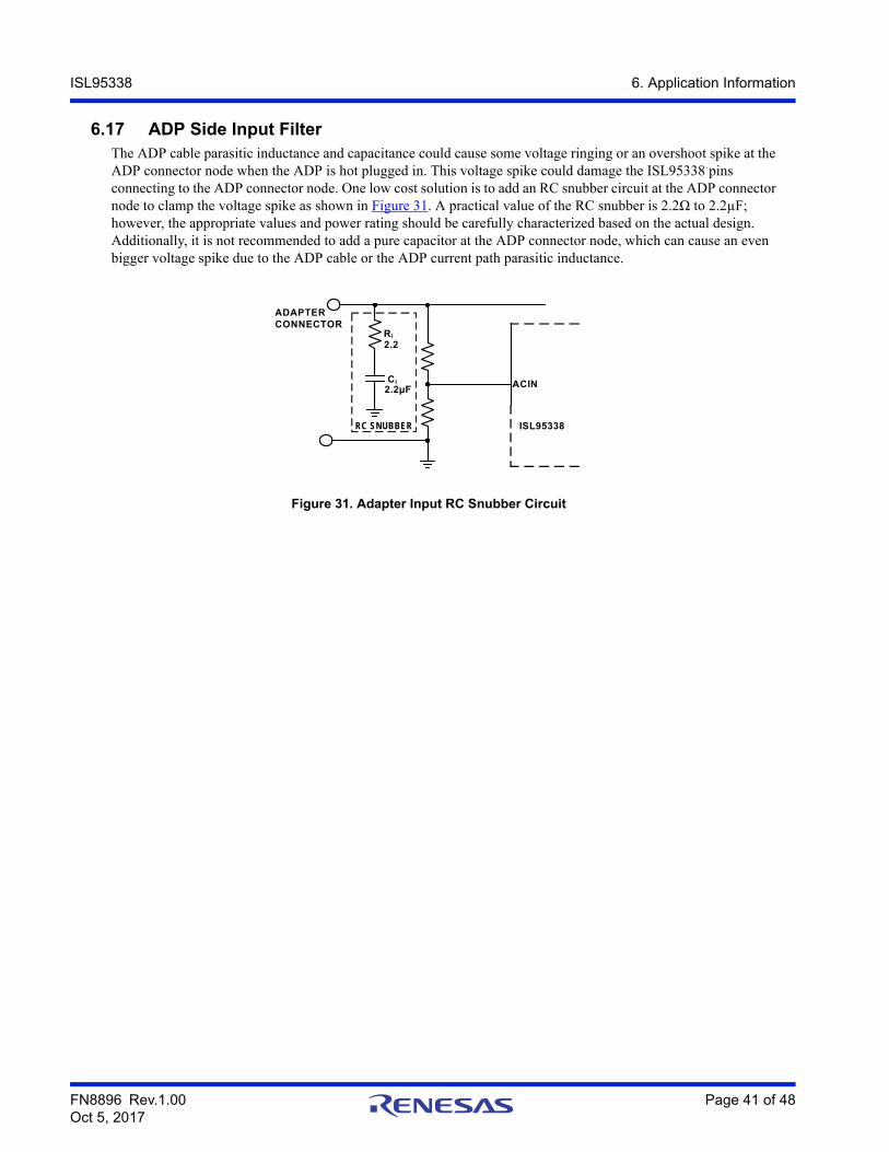
FN8896 Rev.1.00 Page 41 of 48Oct 5, 2017
ISL95338 6. Application Information
6.17 ADP Side Input FilterThe ADP cable parasitic inductance and capacitance could cause some voltage ringing or an overshoot spike at the ADP connector node when the ADP is hot plugged in. This voltage spike could damage the ISL95338 pins connecting to the ADP connector node. One low cost solution is to add an RC snubber circuit at the ADP connector node to clamp the voltage spike as shown in Figure 31. A practical value of the RC snubber is 2.2Ω to 2.2µF; however, the appropriate values and power rating should be carefully characterized based on the actual design. Additionally, it is not recommended to add a pure capacitor at the ADP connector node, which can cause an even bigger voltage spike due to the ADP cable or the ADP current path parasitic inductance.
Figure 31. Adapter Input RC Snubber Circuit
ISL95338
ACIN
ADAPTERCONNECTOR
Ri
Ci
2.2
2.2µF
RC SNUBBER
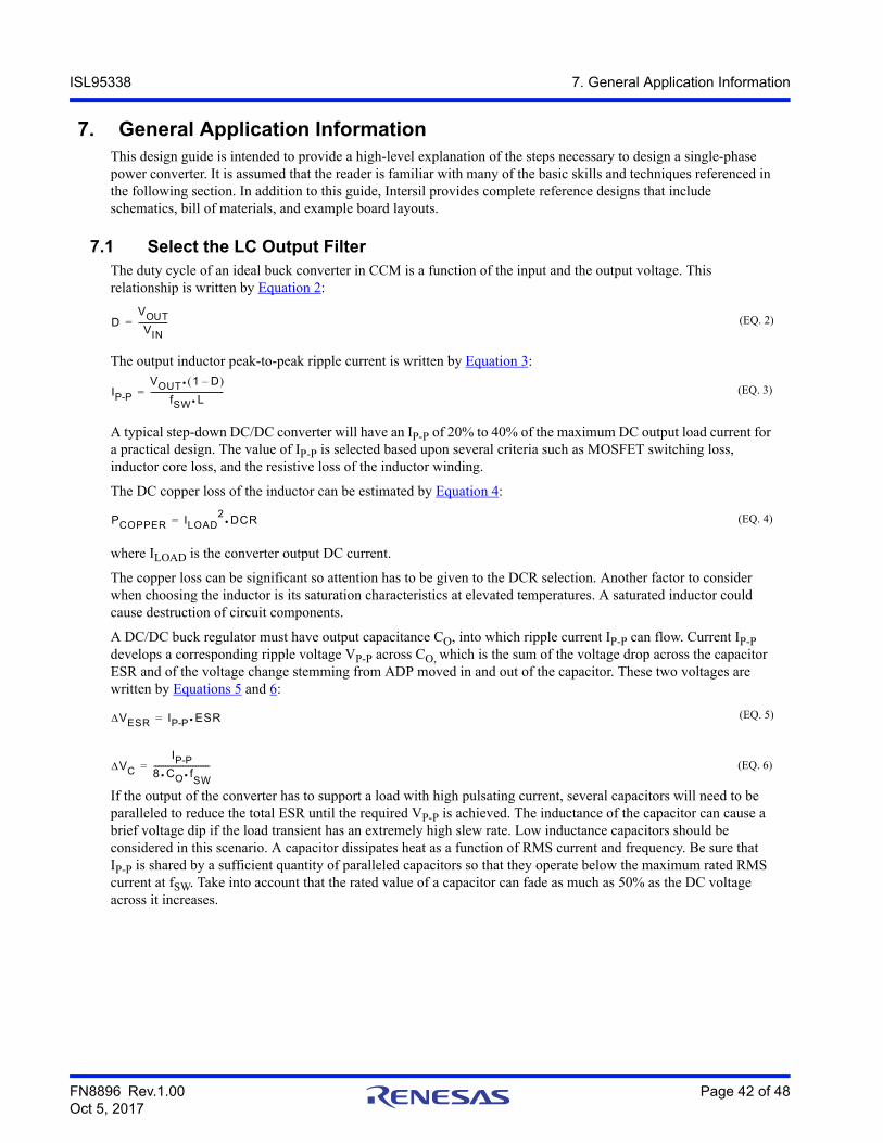
FN8896 Rev.1.00 Page 42 of 48Oct 5, 2017
ISL95338 7. General Application Information
7. General Application InformationThis design guide is intended to provide a high-level explanation of the steps necessary to design a single-phase power converter. It is assumed that the reader is familiar with many of the basic skills and techniques referenced in the following section. In addition to this guide, Intersil provides complete reference designs that include schematics, bill of materials, and example board layouts.
7.1 Select the LC Output FilterThe duty cycle of an ideal buck converter in CCM is a function of the input and the output voltage. This relationship is written by Equation 2:
The output inductor peak-to-peak ripple current is written by Equation 3:
A typical step-down DC/DC converter will have an IP-P of 20% to 40% of the maximum DC output load current for a practical design. The value of IP-P is selected based upon several criteria such as MOSFET switching loss, inductor core loss, and the resistive loss of the inductor winding.
The DC copper loss of the inductor can be estimated by Equation 4:
where ILOAD is the converter output DC current.
The copper loss can be significant so attention has to be given to the DCR selection. Another factor to consider when choosing the inductor is its saturation characteristics at elevated temperatures. A saturated inductor could cause destruction of circuit components.
A DC/DC buck regulator must have output capacitance CO, into which ripple current IP-P can flow. Current IP-P develops a corresponding ripple voltage VP-P across CO, which is the sum of the voltage drop across the capacitor ESR and of the voltage change stemming from ADP moved in and out of the capacitor. These two voltages are written by Equations 5 and 6:
If the output of the converter has to support a load with high pulsating current, several capacitors will need to be paralleled to reduce the total ESR until the required VP-P is achieved. The inductance of the capacitor can cause a brief voltage dip if the load transient has an extremely high slew rate. Low inductance capacitors should be considered in this scenario. A capacitor dissipates heat as a function of RMS current and frequency. Be sure that IP-P is shared by a sufficient quantity of paralleled capacitors so that they operate below the maximum rated RMS current at fSW. Take into account that the rated value of a capacitor can fade as much as 50% as the DC voltage across it increases.
DVOUTVIN
---------------= (EQ. 2)
(EQ. 3)IP-P
VOUT 1 D–
fSW L--------------------------------------=
(EQ. 4)PCOPPER ILOAD2
DCR=
VESR IP-P E SR= (EQ. 5)
VC
IP-P8 CO f
SW
-----------------------------= (EQ. 6)
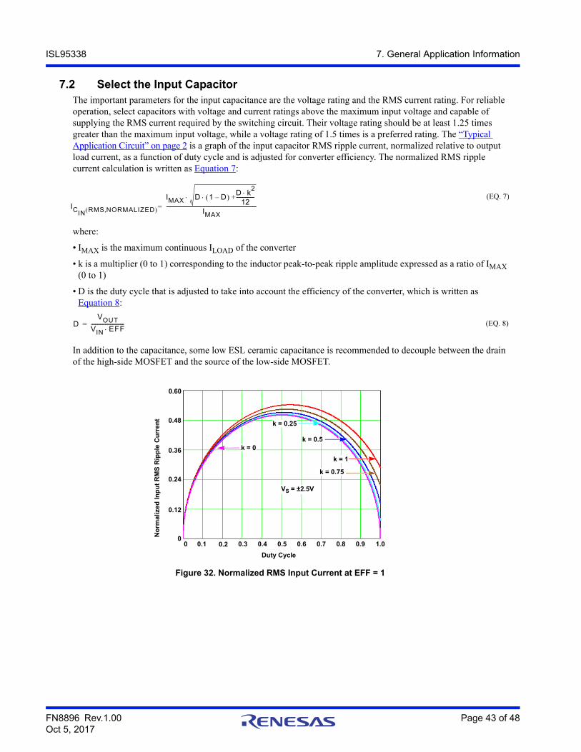
FN8896 Rev.1.00 Page 43 of 48Oct 5, 2017
ISL95338 7. General Application Information
7.2 Select the Input CapacitorThe important parameters for the input capacitance are the voltage rating and the RMS current rating. For reliable operation, select capacitors with voltage and current ratings above the maximum input voltage and capable of supplying the RMS current required by the switching circuit. Their voltage rating should be at least 1.25 times greater than the maximum input voltage, while a voltage rating of 1.5 times is a preferred rating. The “Typical Application Circuit” on page 2 is a graph of the input capacitor RMS ripple current, normalized relative to output load current, as a function of duty cycle and is adjusted for converter efficiency. The normalized RMS ripple current calculation is written as Equation 7:
where:
• IMAX is the maximum continuous ILOAD of the converter
• k is a multiplier (0 to 1) corresponding to the inductor peak-to-peak ripple amplitude expressed as a ratio of IMAX (0 to 1)
• D is the duty cycle that is adjusted to take into account the efficiency of the converter, which is written as Equation 8:
In addition to the capacitance, some low ESL ceramic capacitance is recommended to decouple between the drain of the high-side MOSFET and the source of the low-side MOSFET.
Figure 32. Normalized RMS Input Current at EFF = 1
(EQ. 7)ICIN RMS NORMALIZED,
IMAX D 1 D– D k2
12--------------+
IMAX-----------------------------------------------------------------------=
DVOUT
VIN EFF--------------------------= (EQ. 8)
No
rma
lized
Inp
ut
RM
S R
ipp
le C
urr
en
t
Duty Cycle
0 0.1 0.2 0.3 0.4 0.6 0.7 0.8 0.9 1.00.50
0.12
0.24
0.36
0.48
0.60
k = 0.75
k = 0.5
k = 0.25
k = 0
VS = ±2.5V
k = 1
FN8896 Rev.1.00 Page 44 of 48Oct 5, 2017
ISL95338 7. General Application Information
7.3 Select the Switching Power MOSFETTypically, a MOSFET cannot tolerate even brief excursions beyond their maximum drain-to-source voltage rating. The MOSFETs used in the power stage of the converter should have a maximum VDS rating that exceeds the sum of the upper voltage tolerance of the input power source and the voltage spike that occurs when the MOSFET switches off.
Several power MOSFETs are readily available that are optimized for DC/DC converter applications. The preferred high-side MOSFET emphasizes low gate ADP so that the device spends the least amount of time dissipating power in the linear region. Unlike the low-side MOSFET, which has the drain-to-source voltage clamped by its body diode during turn off, the high-side MOSFET turns off with a VDS of approximately VIN - VOUT, plus the spike across it. The preferred low-side MOSFET emphasizes low rDS(ON) when fully saturated to minimize conduction loss. It should be noted that this is an optimal configuration of MOSFET selection for low duty cycle applications (D < 50%). For higher output, low input voltage solutions, a more balanced MOSFET selection for high- and low-side devices may be warranted.
For the low-side (LS) MOSFET, the power loss can be assumed to be conductive only and is written as Equation 9:
For the high-side (HS) MOSFET, the conduction loss is written as Equation 10:
For the high-side MOSFET, the switching loss is written as Equation 11:
where:
• IVALLEY is the difference of the DC component of the inductor current minus 1/2 of the inductor ripple current
• IPEAK is the sum of the DC component of the inductor current plus 1/2 of the inductor ripple current
• tSW(ON) is the time required to drive the device into saturation
• tSW(OFF) is the time required to drive the device into cut-off
7.4 Select the Bootstrap CapacitorThe selection of the bootstrap capacitor is written by Equation 12:
where:
• Qg is the total gate ADP required to turn on the high-side MOSFET
• VBOOT is the maximum allowed voltage decay across the boot capacitor each time the high-side MOSFET is switched on
As an example, suppose the high-side MOSFET has a total gate ADP Qg of 25nC at VGS = 5V and a VBOOT of 200mV. The calculated bootstrap capacitance is 0.125µF; for a comfortable margin, select a capacitor that is double the calculated capacitance. In this example, 0.22µF will suffice. Use an X7R or X5R ceramic capacitor.
(EQ. 9)PCON_LS ILOAD2
r DS ON _LS 1 D–
(EQ. 10)PCON_HS ILOAD2
r DS ON _HS D=
(EQ. 11)PSW_HS
VIN IVALLEY tSW ON fSW
2------------------------------------------------------------------------------
VIN IPEAK tSW OFF fSW
2---------------------------------------------------------------------------+=
CBOOT
QgVBOOT------------------------= (EQ. 12)
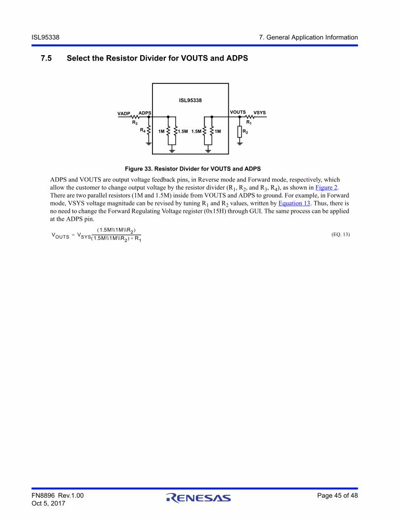
FN8896 Rev.1.00 Page 45 of 48Oct 5, 2017
ISL95338 7. General Application Information
7.5 Select the Resistor Divider for VOUTS and ADPS
Figure 33. Resistor Divider for VOUTS and ADPS
ADPS and VOUTS are output voltage feedback pins, in Reverse mode and Forward mode, respectively, which allow the customer to change output voltage by the resistor divider (R1, R2, and R3, R4), as shown in Figure 2. There are two parallel resistors (1M and 1.5M) inside from VOUTS and ADPS to ground. For example, in Forward mode, VSYS voltage magnitude can be revised by tuning R1 and R2 values, written by Equation 13. Thus, there is no need to change the Forward Regulating Voltage register (0x15H) through GUI. The same process can be applied at the ADPS pin.
1M1M 1.5M1.5M
VOUTSADPS VSYSVADP
ISL95338
R1
R2
R3
R4
VOUTS VSYS
1.5M\\1M\\R2
1.5M\\1M\\R2 R1+---------------------------------------------------------= (EQ. 13)
FN8896 Rev.1.00 Page 46 of 48Oct 5, 2017
ISL95338 8. Revision History
8. Revision History
Rev. Date Description
1.00 Oct 5, 2017 Removed Way Overcurrent Protection (WOCP) function
0.00 Aug 15, 2017 Initial release
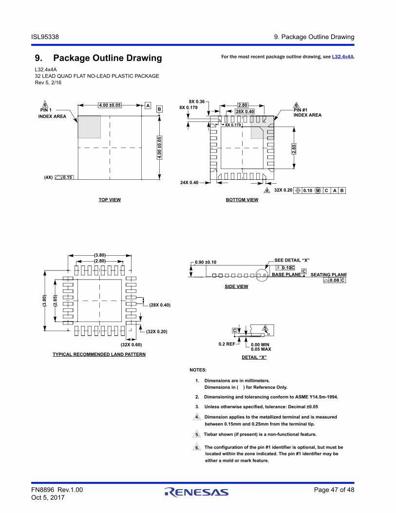
FN8896 Rev.1.00 Page 47 of 48Oct 5, 2017
ISL95338 9. Package Outline Drawing
9. Package Outline DrawingL32.4x4A32 LEAD QUAD FLAT NO-LEAD PLASTIC PACKAGE Rev 5, 2/16
BOTTOM VIEW
DETAIL “X”
SIDE VIEW
TYPICAL RECOMMENDED LAND PATTERN
TOP VIEW
located within the zone indicated. The pin #1 identifier may be
Unless otherwise specified, tolerance: Decimal ±0.05
Tiebar shown (if present) is a non-functional feature.
The configuration of the pin #1 identifier is optional, but must be
between 0.15mm and 0.25mm from the terminal tip.
Dimension applies to the metallized terminal and is measured
Dimensions in ( ) for Reference Only.
Dimensioning and tolerancing conform to ASME Y14.5m-1994.
6.
either a mold or mark feature.
3.
5.
4.
2.
Dimensions are in millimeters.1.
NOTES:
PIN #16
B0.10 M AC32X 0.20
24X 0.40
2.65
8X 0.179
8X 0.179
8X 0.36
28X 0.40INDEX AREA
PIN 16 A
B
(4X) 0.15
CSEATING PLANEBASE PLANE
0.08
SEE DETAIL “X”
C
C0.10// 0.90 ±0.10
0.00 MIN0.05 MAX
5
0.2 REF(32X 0.60)
(32X 0.20)
(28X 0.40)
(2.80)(3.80)
(3.8
0)
(2.6
5)
2.80
C
4
INDEX AREA
4.00 ±0.05
4.0
0 ±
0.0
5
For the most recent package outline drawing, see L32.4x4A.
FN8896 Rev.1.00 Page 48 of 48Oct 5, 2017
ISL95338 10. About Intersil
Intersil products are manufactured, assembled and tested utilizing ISO9001 quality systems as notedin the quality certifications found at www.intersil.com/en/support/qualandreliability.html
Intersil products are sold by description only. Intersil may modify the circuit design and/or specifications of products at any time without notice, provided that such modification does not, in Intersil's sole judgment, affect the form, fit or function of the product. Accordingly, the reader is cautioned to verify that datasheets are current before placing orders. Information furnished by Intersil is believed to be accurate and reliable. However, no responsibility is assumed by Intersil or its subsidiaries for its use; nor for any infringements of patents or other rights of third parties which may result from its use. No license is granted by implication or otherwise under any patent or patent rights of Intersil or its subsidiaries.
For information regarding Intersil Corporation and its products, see www.intersil.com
For additional products, see www.intersil.com/en/products.html
© Copyright Intersil Americas LLC 2017. All Rights Reserved.All trademarks and registered trademarks are the property of their respective owners.
10. About IntersilIntersil Corporation is a leading provider of innovative power management and precision analog solutions. The company's products address some of the largest markets within the industrial and infrastructure, mobile computing, and high-end consumer markets.
For the most updated datasheet, application notes, related documentation, and related parts, see the respective product information page found at www.intersil.com.
For a listing of definitions and abbreviations of common terms used in our documents, visit www.intersil.com/glossary.
You can report errors or suggestions for improving this datasheet by visiting www.intersil.com/ask.
Reliability reports are also available from our website at www.intersil.com/support.

Mouser Electronics
Authorized Distributor
Click to View Pricing, Inventory, Delivery & Lifecycle Information: Intersil:
ISL95338HRTZ-T7A