one-cycle-controlled bidirectional ac-to-dc converter with
TRANSCRIPT

IEEE TRANSACTIONS ON INDUSTRIAL ELECTRONICS, VOL. 56, NO. 5, MAY 2009 1499
One-Cycle-Controlled Bidirectional AC-to-DCConverter With Constant Power Factor
Dharmraj V. Ghodke, Sreeraj E. S., Kishore Chatterjee, and B. G. Fernandes
Abstract—Grid-connected unity-power-factor converters basedon one-cycle control (OCC) do not require the service of phase-locked loop or any other synchronization circuits for interfacingwith the utility. As a result, these schemes are becoming increas-ingly popular. However, as the power handled by the converterincreases, the power factor deteriorates. To understand quantita-tively the cause of poor power factor while negotiating high powerloads, large signal models for these schemes are developed. Havingunderstood the cause for poor power factor operation, a modified-OCC-based converter is proposed. This scheme has high powerfactor while supplying high power loads. Detailed simulation stud-ies are carried out to verify the efficacy of the scheme. In order toconfirm the viability of the scheme, detailed experimental studiesare carried out on a 3-kW laboratory prototype.
Index Terms—AC–DC power conversion, one-cycle controller,power-factor correction, single- and three-phase rectifier.
I. INTRODUCTION
T RADITIONALLY, diode or thyristor bridge rectifiers areemployed to obtain dc voltage from ac main. These rec-
tifiers pollute the utility with low-order harmonics, which aredifficult to filter. Pulsewidth-modulated (PWM) converters areused to overcome this problem. They shift the frequency of thedominant harmonics to a higher value so that these harmonicscan be eliminated by employing a small passive filter [1]. ThePWM bidirectional converter draws a near sinusoidal inputcurrent while providing a regulated output dc voltage and canoperate in the first and second quadrants of the voltage–currentplane [2]. Generally, the control structure of a three-phase six-switch PWM boost converter consists of an inner current and anouter voltage control loop [2]–[6], [10]–[16]. The current con-troller senses the input current and compares it with a sinusoidalcurrent reference. In order to obtain this reference, the phaseinformation of the utility voltages or current is required. Gener-ally, this information is obtained by employing a phase-lockedloop (PLL) (or current phase observer technique) [7]–[9].Grid-connected converters based on basic one-cycle control(B-OCC) do not require the service of PLL or zero crossingdetectors to synchronize with the grid and can be designed to
Manuscript received March 7, 2008; revised December 3, 2008. First pub-lished January 9, 2009; current version published April 29, 2009.
D. V. Ghodke is with the Raja Ramanna Centre for Advanced Technology,Indore 452013, India (e-mail: [email protected]).
Sreeraj E. S. is with the Department of Electrical Engineering, IndianInstitute of Technology Bombay, Mumbai 400076, India.
K. Chatterjee and B. G. Fernandes are with the Department of ElectricalEngineering, Indian Institute of Technology Bombay, Mumbai 400076, India(e-mail: [email protected]; [email protected]).
Color versions of one or more of the figures in this paper are available onlineat http://ieeexplore.ieee.org.
Digital Object Identifier 10.1109/TIE.2009.2012414
Fig. 1. Single-phase full-bridge converter.
supply power at power factors near to unity. As a result, theyare becoming increasingly popular [3]–[5], [10]. Moreover,in these schemes, the switching frequency of the devices isheld constant. This is an attractive feature for high powerconverters. However, OCC-based schemes exhibit instabilityin operation, when the converter is lightly loaded [3], [10],[12], [16]. Moreover, these converters cannot shift its operationfrom rectifying to inverting mode of operation, as would be thecase if the converter was required to negotiate active type ofloads. In order to address these limitations, a modified-OCC(M-OCC)-based scheme has been presented in [12] and [13]. Inall the aforementioned schemes based on OCC, the power fac-tor decreases under certain operating condition. This problembecomes prominent at low switching frequencies. In this paper,reasons for this limitation are analyzed. Having understood thereasons for low power factor operation, a constant power factorone-cycle controller for single-phase full bridge and three-phase six-switch boost bidirectional converter is proposed. Thiscontroller enables the converters to operate at constant and nearunity power factor even for a wide variation in load. Detailedanalytical and simulation studies are carried out to verify theefficacy of the scheme. In order to confirm the viability ofthe scheme, detailed experimental studies are carried out on ascaled down 3-kW laboratory prototype.
II. ONE-CYCLE-CONTROLLED AC-TO-DC CONVERTER
The schematic power circuit diagrams of single-phase fullbridge and three-phase six-switch boost bidirectional convert-ers are shown in Figs. 1 and 2, respectively. Although thebasic working principle of OCC-based single-phase converteris presented in [13], for the sake of completeness, it is brieflydescribed in this paper. The dc-side capacitor voltage (νO) issensed and compared with a reference voltage (V ∗
O), and theerror is compensated by a proportional–integral (PI) control-ler to produce a modulating reference signal (VM ). A bipolar
0278-0046/$25.00 © 2009 IEEE

1500 IEEE TRANSACTIONS ON INDUSTRIAL ELECTRONICS, VOL. 56, NO. 5, MAY 2009
Fig. 2. Three-phase six-switch boost converter.
sawtooth waveform whose peak-to-peak value of 2VM is gen-erated. The frequency of the sawtooth waveform is set by a freerunning clock, which also sets the switching frequency of theconverter. The sensed boost inductor current iS is comparedwith the sawtooth waveform. At every rising edge of the clockpulse, S2 and S4 are turned on. The inductor current, which isalso the source current, increases with a slope of K1, and this isgiven by
K1 = Rs(νS + VO)
L(1)
where νS is the utility voltage, L is the inductance of the boostinductor, and Rs is the gain of the source current sensor. Whenthe magnitude of boost inductor current becomes equal to thatof the sawtooth waveform, S2 and S4 are turned off, and S1 andS3 are turned on. The boost inductor current falls with a slopeK2; this is given by
K2 = Rs(νS − VO)
L. (2)
It has been shown in [13] that the peak value of current ineach switching cycle is given by
iS =(VMνS)(VORS)
. (3)
It can be inferred from (3) that source current magnitude isproportional to the source voltage and is in phase with it. Thepower handled by the converter is given by
P ≈(VMV 2
S
)VoRS
(4)
where Vs is the rms value of the source voltage.A control block diagram for the three-phase scheme is ex-
plained in detail in [10]. In this case, the phase current isgiven by
in =(VMνn)(2VORS)
, n = A,B,C (5)
and the total power handled by the converter is
P ≈(3 · VMV 2
S
)2 · VoRS
(6)
TABLE IPERFORMANCE OF B-OCC-BASED THREE-PHASE CONVERTER
TABLE IIPERFORMANCE OF M-OCC-BASED THREE-PHASE CONVERTER
where VS is the rms value of each phase voltage. From (3)and (5), it can be concluded that the source current and volt-ages are in phase. However, this holds good only under theassumption that the average voltage across the inductor in everyswitching cycle is zero. This is true only at high switchingfrequency. Moreover, operation of the converter based on theaforementioned scheme is unstable during light load conditionand can function only as a rectifier [3], [10]. To address theselimitations, a modified scheme is proposed in [12] and [13].The performance of the converter utilizing this technique isstable at light load condition, and more importantly, powerflow can now be bidirectional. In this technique, three fictitiouscurrent signals iFn(n = A,B,C), which are proportional tothe respective phase voltages (iF = Vn/RF n = A,B,C) andin phase with three utility voltages, are synthesized. Thesecurrent signals are added to the boost inductor current signals,and their sum is compared with the sawtooth waveform togenerate gating pulses for the converter switches.
A. Demonstration of Low Power Factor Operation
Converters with the aforementioned schemes [3], [10], [12],[13] operate at considerably low power factor as the powerhandled by the converter increases. This problem becomesprominent at lower switching frequencies. This feature of theB-OCC-based converter proposed in [3] and [10] is demon-strated in Table I and that of the M-OCC-based converterproposed in [12] and [13] in Table II.
III. LARGE-SIGNAL MODELS FOR
B-OCC-BASED CONVERTERS
A. B-OCC-Based Single-Phase Converter
The problem of poor power factor operation of B-OCC-based converters while negotiating high power loads has not yetbeen quantitatively assessed. In order to understand the reason

GHODKE et al.: BIDIRECTIONAL AC-TO-DC CONVERTER WITH CONSTANT POWER FACTOR 1501
Fig. 3. (a) Generation of switching logic for single-phase B-OCC-basedconverter presented in [3]. (b) Phasor model of single-phase B-OCC-basedconverter presented in [3].
for low power factor operation of B-OCC-based converterswhile negotiating high power loads, an effort has been madeto develop large signal models of these converters. Using thesemodels, the trajectory of the peak value of source current drawnby the converter in each switching cycle can be determined.When the switches S2 and S4 are on for the duration of t1,inductor current rises with the slope K1 (1), while for theduration t2, current falls with the slope of K2 (2).
The inductor current waveform, which is also the sourcecurrent at the N th and (N + 1)th switching cycles, along withthe sawtooth waveform, is shown in Fig. 3(a). The peak valueof current in N th switching cycle is IN , and I∗N denotes themagnitude of current at the end of N th switching cycle.
From Fig. 3(a),
RSI∗N = RSIN
(1 − K2
K3
)+ VM
K2
K3(7)
IN+1 = I∗N + K1t1 = VM − K3t1 (8)
where K3 is the slope of the falling edge of the sawtoothwaveform and is given by
K3 =VM
TI=
(2VM
TS
)=
(2VORS
ReTS
)(9)
and Ts is the switching time period. Assuming that the changein on time (t1) of the switch in two consecutive switching
cycles is small, and using (7) and (8), the durations of t1 andt2 from Fig. 3(a) are
t1 =VM − RSIN + (RSIN + VM )K2
K3
K3 + K1(10)
t2 =(RSIN + VM )
K3 + K1. (11)
The change in current ΔiS from the N th to (N + 1)th cycle intime TS(= t1 + t2) is
ΔiS = IN+1 − IN =VS
L(t1 + t2) +
VO
L(t1 − t2). (12)
Substituting K1, K2, and K3 from (1), (2) and (9) in (10)–(12)
νS = LΔiSΔt
+RSiSVO
VM. (13)
Considering the switching time period to be small, (13) can beapproximated as
νS = LdiSdt
+RSiSVO
VM. (14)
Considering νs to be a sinusoidal forcing function and neglect-ing the harmonics in is, the steady state phasor form of (14) canbe approximated as
iS =νS
RSVO
VM+ jωL
. (15)
Based on (15), the steady state model of the system is shown inFig. 3(b). It can be inferred that, if ωL is small compared to theratio of VO and VM , the system operates close to unity powerfactor. However, VM is proportional to the operating powerlevel, as depicted in (4). As a result, the power factor of theconverter decreases as the power negotiated by the converterincreases. The problem of operation with low power factor getsmore prominent if the converter is designed to operate at lowswitching frequency with higher value of boost inductor, whichis generally the case in medium and high power levels.
B. B-OCC-Based Three-Phase Converter
The sawtooth waveform, along with the three-phase currentsdrawn at a particular switching cycle, wherein iA > iB > iC ,is shown in Fig. 4(a). The duration for which iA, iB , andiC are less than the sawtooth waveform is t1, while t4 is theduration for which iA, iB , and iC are greater than the sawtoothwaveform. The duration for which only iA is higher than thesawtooth is t2, while t3 is the duration for which only ic is lessthan the sawtooth waveform. The slopes of the source currentsof each phase n (where n is a, b, or c) for the time durations t1,t2, t3, and t4 are K1n, K2n, K3n, and K4n, respectively, andare listed in Table III.
Since the utility considered is a three-phase three-wiresystem
iA + iB + iC = 0 (16)

1502 IEEE TRANSACTIONS ON INDUSTRIAL ELECTRONICS, VOL. 56, NO. 5, MAY 2009
Fig. 4. (a) Generation of switching logic for three-phase B-OCC-based con-verter presented in [3]. (b) Phasor model of three-phase B-OCC-based ac-to-dcconverter presented in [3].
TABLE IIISLOPES OF PHASE CURRENTS AT VARIOUS SWITCHING INSTANTS
therefore,
t3 =IB − IC
K3t2 =
IA − IB
K3(17)
where IA, IB , and IC denote the magnitude of iA, iB , and iCat the instants where they intersect with the falling slope of thesawtooth waveform. The change in phase-A current ΔiA duringa switching cycle (Δt = Ts) is given by
ΔiA =νA
LATS − VO
3LA(2t2 + t3). (18)
Combining (17) and (18) and using (16)
νA = LAΔiATS
+RSiAVO
K3TS. (19)
Substituting K3 from (17) and considering the switching timeperiod to be small, (19) can be approximated as
νA = LAdiAdt
+RSiAVO
2VM. (20)
Considering νA to be a sinusoidal forcing function and neglect-ing the harmonic content in iA, the steady state phasor form of(20) can be approximated for phase-A as
iA =νA
RSVO
2VM+ jωLA
. (21)
Therefore, three-phase source currents can be represented as
in =νn
RSVO
2VM+ jωLn
, n = A,B,C. (22)
Based on (22), the steady-state per-phase phasor model ofthe system is shown in Fig. 4(b). It can be inferred that, ifωL is small compared to the ratio of VO and VM , the sourcepower factor is approximately unity. Since VM is proportionalto the operating power level, the power factor decreases withincreases in power.
IV. LARGE-SIGNAL MODELS FOR
M-OCC-BASED CONVERTERS
A. Modified Single-Phase OCC Converter
In this converter, switching pulses are generated by compar-ing the sum of the source current signal (RSiS) and the fic-titious current signal iF RS = (RS/RF )νS with the sawtoothwaveform, as shown in Fig. 5(a), where RF is the resistance togenerate fictitious current (iF ). Therefore,
RSiO = RS(iS + iF ) = RS
(iS +
1RF
νS
). (23)
The change in peak current between two switching cycles is
ΔiS =K1t1+K2t2 =(
νS +VO
L
)t1+
(νS−VO
L
)t2. (24)
Therefore,
LΔiSTS
= VS − VO
VMRSiF . (25)
Combining (23) and (25),
LΔiSTS
= νS − RSVO
VM
(iS +
1RF
νS
). (26)
Considering the switching time period Ts to be small, (26) canbe approximated as
RSVO
VMiS + L
diSdt
= νS
(1 − RS
RF
VO
VM
). (27)

GHODKE et al.: BIDIRECTIONAL AC-TO-DC CONVERTER WITH CONSTANT POWER FACTOR 1503
Fig. 5. (a) Generation of switching logic for the M-OCC-based single-phaseconverter presented in [12]. (b) Phasor model of single-phase M-OCC-basedconverter presented in [12].
The steady-state phasor form of (27) can be approximated as
iS =V S
(1 − RS
RF
VO
VM
)RSVO
VM+ jωL
. (28)
Based on (28), the steady-state phasor model of the system isshown in Fig. 5(b). The conclusions made in the previous caseare also valid in this case.
B. M-OCC-Based Three-Phase Converter
As shown in Fig. 6(a), the sum of phase current signal andthe fictitious current signal inF RS = (RS/RF )νn is comparedwith the sawtooth waveform. At the point of intersection of thewaveform, the following can be written:
ieff(n) =RS(inf +iLn)=RS
(Vn
RF+iLn
), n=A,B,C.
(29)Moreover,
t2 =IOA − IOB
K3t3 =
IOB − IOC
K3. (30)
The change in current in phase-A in a switching cycle isgiven by
ΔIA =νA
LA(TS) − νA
3LA(t3 + 2t2). (31)
Fig. 6. (a) Generation of switching logic for three-phase M-OCC-basedconverter presented in [12]. (b) Phasor model of three-phase M-OCC-basedac-to-dc converter presented in [12].
Combining (29) and (31) and considering TS to be small, (31)can be approximated as
RSVO
2VMiA + LA
diAdt
= νA
(1 − RS
RF
VO
2VM
). (32)
Considering νA to be a sinusoidal forcing function and neglect-ing the harmonic in iA, the steady state phasor form of (32) canbe represented as
iA =νA
(1 − RS
RF
VO
2VM
)RSVO
2VM+ jωLA
. (33)
Similarly, three-phase inductor currents are given by
in =νn
(1 − RS
RF
VO
2VM
)RSVO
2VM+ jωLn
, n = A,B,C. (34)
Based on (34), the steady state phasor model of the systemis shown in Fig. 6(b). In addition to the conclusions drawnin Section IV, from models shown in Figs. 5(b) and 6(b), itcan be inferred that, for (1/RF )(VO/2VM ) < 1, the converteroperates in rectifying mode and, for (1/RF )(VO/2VM ) > 1,the converter operates in the inverting mode.
1504 IEEE TRANSACTIONS ON INDUSTRIAL ELECTRONICS, VOL. 56, NO. 5, MAY 2009
Fig. 7. (a) Equivalent circuit of the single-phase converter when switchesS2 and S4 conduct. (b) Equivalent circuit of the single-phase converter whenswitches S1 and S3 conduct.
V. PROPOSED CPF-OCC-BASED CONVERTER
In order to understand the cause for low power factor op-eration when the OCC-based converters are delivering largemagnitude of load, the basic principle of operation of OCC-based converters, which is presented in detail in [3] and brieflypresented in Section II, is again been repeated here. Consideringthe schematic power circuit diagram of single-phase convertershown in Fig. 1, switch pairs S1–S3 and S2–S4 are operatedwith a switching time period of Ts such that S2–S4 are on fora time duration of DTs and S1–S3 are on for a time durationof (1 − D)Ts. The pertinent equivalent circuits are shown inFig. 7(a) and (b). The switching frequency of the switchingdevices is 1/Ts.
If Ts is assumed to be small, referring to Fig. 1, I∗N ≈ I∗N+1,therefore, the average voltage drop across the inductor L can beequated to zero, as given in
(νs + Vo)DTs + (νs − Vo)(1 − D)Ts = 0. (35)
Hence,
νs = (1 − 2D)Vo. (36)
Now, if is has to be a sinusoidal current in phase with νs, ithas to be made proportional to νs. Defining this proportionalityconstant to be Re
νs = isRsRe (37)
wherein Rs is the gain of the source current sensor. Theconstant Re represents the effective emulated resistance that isbeing viewed by an ac source when the converter is feeding acertain load and drawing in phase current is from the source.Therefore, to have a unity power factor operation, the conditionthat has to be fulfilled is obtained by combining (36) and(37) as
isRsRe = (1 − 2D)Vo. (38)
Defining
VM =V0
Re(39)
(38) transforms to
VM (1 − 2D) = RsiS . (40)
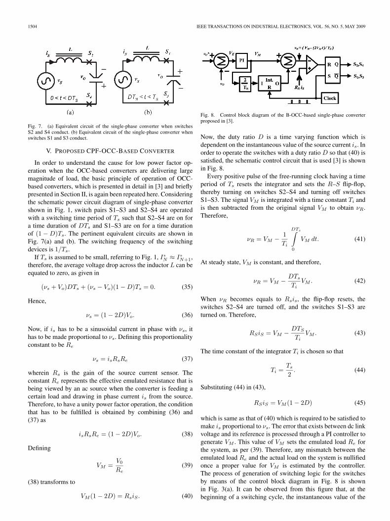
Fig. 8. Control block diagram of the B-OCC-based single-phase converterproposed in [3].
Now, the duty ratio D is a time varying function which isdependent on the instantaneous value of the source current is. Inorder to operate the switches with a duty ratio D so that (40) issatisfied, the schematic control circuit that is used [3] is shownin Fig. 8.
Every positive pulse of the free-running clock having a timeperiod of Ts resets the integrator and sets the R–S flip-flop,thereby turning on switches S2–S4 and turning off switchesS1–S3. The signal VM is integrated with a time constant Ti andis then subtracted from the original signal VM to obtain νR.Therefore,
νR = VM − 1Ti
DTs∫0
VM dt. (41)
At steady state, VM is constant, and therefore,
νR = VM − DTs
TiVM . (42)
When νR becomes equals to Rsis, the flip-flop resets, theswitches S2–S4 are turned off, and the switches S1–S3 areturned on. Therefore,
RSiS = VM − DTS
TiVM . (43)
The time constant of the integrator Ti is chosen so that
Ti =Ts
2. (44)
Substituting (44) in (43),
RSiS = VM (1 − 2D) (45)
which is same as that of (40) which is required to be satisfied tomake is proportional to νs. The error that exists between dc linkvoltage and its reference is processed through a PI controller togenerate VM . This value of VM sets the emulated load Re forthe system, as per (39). Therefore, any mismatch between theemulated load Re and the actual load on the system is nullifiedonce a proper value for VM is estimated by the controller.The process of generation of switching logic for the switchesby means of the control block diagram in Fig. 8 is shownin Fig. 3(a). It can be observed from this figure that, at thebeginning of a switching cycle, the instantaneous value of the

GHODKE et al.: BIDIRECTIONAL AC-TO-DC CONVERTER WITH CONSTANT POWER FACTOR 1505
source current I∗N is not equal to its instantaneous value I∗N+1
at the end of that switching cycle. This is due to the fact thatthe magnitude of forcing function νs is also changing within aswitching cycle. If
I∗N − I∗N+1 =Δi (46)
Δi =0 (47)
the condition depicted by (35) is valid, and is is in phase withνs, as shown earlier. Now, as Δi �= 0, the condition of (35)is not valid, and hence, is would not be in phase with νs.The larger is the magnitude of |Δi|, the more is the phaseshift that is introduced between νs and is, and hence, the pooris the power factor of the system. From Fig. 3(a), it can beinferred that |Δi| increases with increment in VM , as wellas with increment in Ts. Now, VM increases with incrementin load negotiated by the converter, as depicted in (39), andTs increases if the system is designed for a lower value ofswitching frequency. Therefore, as the load on the OCC-basedconverter is increased or the switching frequency is reduced, thepower factor of these converters falls. In the case of M-OCC-based bidirectional ac-to-dc converter proposed in [13], thefictitious current component iF is added with is, and then, thissignal is compared with the sawtooth waveform. Therefore,the amplitude of VM is more in this case compared to thatof B-OCC-based converter for the same amount of load beingnegotiated. Hence, the power factor of M-OCC-based converteris less compared to that of B-OCC-based converter when theload negotiated by both of them remains the same for a givenswitching frequency. This feature of OCC-based converters isquantitatively corroborated by deriving the large signal modelsof these systems in Sections III and IV. From the analysespresented earlier and also from the large signals models derivedin the previous sections, it can be inferred that the amplitudeof the sawtooth waveform determines the power drawn fromthe source and the power factor. The amplitude of the sawtoothwaveform increases with an increase in power drawn fromthe source. As a result, the power factor decreases. Hence,by some means, if the amplitude of the sawtooth waveform iskept small and is maintained constant throughout the operatingrange, high power factor can be maintained. Models shown inFigs. 5(b) and 6(b) suggest that power level can be changedif 1/RF is varied in sympathy with the power requirementof the load while maintaining VM constant. Based on theseobservations, in the control scheme of the OCC-based converterproposed in this paper, the amplitude of the sawtooth waveformis maintained constant, and its value is kept low. Furthermore,the amplitude of signals obtained after multiplying the utilityvoltages by 1/RF is multiplied by the error existing betweenthe sensed dc link voltage and the dc link voltage reference.This ensures that the magnitude of the signal, which is inphase with the utility voltages, gets modulated as per the powerrequirement of the load. The equations describing the behaviorof the proposed constant power factor OCC (CPF-OCC)-basedconverter remain the same as that of (28) and (34). The detailedstructure of the controller of the proposed scheme is explainedin the following section.
Fig. 9. (a) Control block diagram of the proposed CPF-OCC-based single-phase converter. (b) Control block diagram of the proposed CPF-OCC-basedthree-phase converter.
TABLE IVPARAMETERS USED FOR THE SIMULATION MODEL AND
LABORATORY PROTOTYPE OF THE SYSTEM
A. CPF-OCC-Based Single-Phase Converter
The schematic control block diagram of the proposed con-verter for single-phase case is shown in Fig. 9(a). The dc linkcapacitor voltage νO is sensed and compared with the referencevoltage V ∗
O. The error so generated is fed to a PI controller.The fictitious current signal iF , which is proportional to thesource voltage, is generated by multiplying νS by 1/RF . Theinverted output (−νe) of the PI controller is multiplied withiF to generate the signal im. The sum of im and the signal

1506 IEEE TRANSACTIONS ON INDUSTRIAL ELECTRONICS, VOL. 56, NO. 5, MAY 2009
Fig. 10. Schematic test setup for three-phase six-switch boost converter in rectifying and inverting modes of operations.
proportional to the source current (im + RSis) is then com-pared with the sawtooth waveform (νR). Unlike in the earlierschemes based on OCC, the amplitude of the sawtooth wave-form is maintained constant. Moreover, here, its magnitude iskept small so that the power factor of the system is maintainedhigh. A free running clock sets the frequency of this sawtoothwaveform. At every rising edge of the clock pulse, S2 and S4
are turned on. When the sum (im + RSis) becomes equal to thesawtooth waveform, S2 and S4 are turned off, and S1 and S2 areturned on.
B. CPF-OCC-Based Three-Phase Converter
The controller for the three-phase case is shown in Fig. 9(b),and the principle of operation remains almost the same as thatof the single-phase converter. The inverted output of the PI con-troller is multiplied by signals proportional to individual phasevoltages to generate fictitious current signals for the individualphases. These fictitious currents signals (RSiFn n = A,B,C)are then added to the signals proportional to the correspondingphase current signals (RSin n = A,B,C). The three signalsso generated are compared with a common sawtooth waveformof constant magnitude (νR). At the rising edge of each clockpulse S2, S4 and S6 are turned on. When the sum of each phasecurrent and the fictitious current becomes equal to the sawtoothwaveform, upper switches are turned on, and the lower switchesare turned off.
VI. SIMULATION AND EXPERIMENTAL RESULTS
The proposed one-cycle-controlled constant power factorthree-phase converter is simulated on MATLAB/Simulink plat-form. The parameters used for simulation studies are given inTable IV. The schematic power circuit diagram used for thestudy is shown in Fig. 10. The single pole double throw (SPDT)switch changes the mode of operation of the converter fromrectifying to inverting as the switch position is changed from2 to 1. When the converter is operating in inverting mode, theaverage power fed back to the utility is given by
Pinv =(
VG − Vo
Rc
)Vo. (48)
TABLE VCOMPARISON OF THE POWER FACTOR OF THE PROPOSED CONVERTER
WITH OTHER OCC-BASED CONVERTERS
Fig. 11. Variation of power factor with load for three-phase converters(B-OCC [3], M-OCC [12], and CPF-OCC).
Moreover, while in the rectifying mode, the power drawn fromthe utility is given by
Prect =V 2
o
RL. (49)
The variation in power factor with load for B-OCC- andM-OCC-based converters and the proposed CPF-OCC-basedconverter is provided in Table V, and it is shown graphicallyin Fig. 11. It can be inferred from this figure that OCC-based

GHODKE et al.: BIDIRECTIONAL AC-TO-DC CONVERTER WITH CONSTANT POWER FACTOR 1507
Fig. 12. (a) Simulated results of B-OCC-based three-phase converter operat-ing in rectifying mode (phase delay 12.04◦). (b) Simulated results of M-OCC-based three-phase converter operating in rectifying mode (phase delay 23.75◦).(c) Simulated results of proposed CPF-OCC-based three-phase converter oper-ating in rectifying mode (phase delay 2.56◦).
Fig. 13. Transient performance of the proposed CPF-OCC-based three-phaseconverter. (Transition from inverting to rectifying mode and back to invertingmode).
TABLE VIPARAMETERS USED FOR THE LABORATORY PROTOTYPE OF
THE PROPOSED ONE-CYCLE-CONTROLLER-BASED
BIDIRECTIONAL CONVERTER
constant power factor converter operates at almost unity powerfactor for all load conditions. The steady state responses duringthe rectifier mode of operation of the B-OCC-, M-OCC-, andCPF-OCC-based converters are shown in Fig. 12(a)–(c). Theload negotiated by the converter in all cases is 20 kW. It canbe observed from Fig. 12(a) that, in the case of B-OCC-basedconverter, the source current lags the source voltage by 12.04◦,while the angles for M-OCC-based converter [Fig. 12(b)] andthe proposed CPF-OCC-based converter [Fig. 12(c)] are 23.75◦
and 2.56◦, respectively. The transient performance of the CPF-OCC-based converter is shown in Fig. 13. The load negotiatedby the converter is changed from 20 to −20 kW at 0.08 sand from −20 to 20 kW at 0.12 s. From the results, it can beinferred that the dynamic response of the system is quite fast,and no instability in the source current is observed during theoperation.
In order to confirm the viability of the proposed CPF-OCC-based three-phase converter, a 3-kW laboratory prototype isdeveloped, and detailed experimental studies are carried out.The schematic power circuit of the experimental setup remainsessentially the same as that of Fig. 10. The parametric values ofthe components used to fabricate the power circuit of the proto-type are provided in Table VI. In order to have the performanceequivalence between the simulation and laboratory model, the

1508 IEEE TRANSACTIONS ON INDUSTRIAL ELECTRONICS, VOL. 56, NO. 5, MAY 2009
Fig. 14. (a) Experimental result of M-OCC-based converter operating inrectifying mode. (CH1) Phase-A voltage (νA; 100 V/div). (CH2) Phase-Bcurrent (iB ; 4 A/div). (CH3) Phase-C current (iC ; 4 A/div). (CH4) Phase-A current (iA; 4 A/div). (Time scale) 10 ms/div. (b) Experimental result ofB-OCC-based converter operating in rectifier mode. (CH1) Phase-A voltage(νA; 100 V/div). (CH2) Phase-B current (iB ; 4 A/div). (CH3) Phase-C current(iC ; 4 A/div). (CH4) Phase-A current (iA; 2 A/div). (Time scale) 10 ms/div.
size of the boost inductor in the hardware prototype is chosentwice than that of the simulation model. This is required, asthe chosen switching frequency of the laboratory prototype istwice that of the switching frequency of the simulation model.The measured steady state performance of the M-OCC-basedthree-phase ac-to-dc converter operating in rectifying mode isshown in Fig. 14(a). It can be seen from this figure that the anglebetween source voltages and the corresponding currents is−33.00◦. The steady state performances during rectifying modeof operation of the B-OCC-based three-phase ac-to-dc con-verter and the proposed converter are shown in Figs. 14(b) and15(a), respectively. The phase angle between the source voltageand the corresponding current in B-OCC-based converter is15.68◦ while that in the proposed converter is 7.34◦. It canbe observed from the harmonic spectrum of phase-A current,which is shown in Fig. 15(a), that low-order current harmonicsare absent in the input current waveform of the converter.
Fig. 15. (a) Experimental result of proposed CPF-OCC-based converter oper-ating in rectifying mode of operation. (CH1, CH2, CH3) Three-phase currents(iA), (iB), and (iC) (10 A/div). (CH4) Phase voltage (νA; 100 V/div). (Ch-M)Harmonic spectrum of phase-A current (0.5 A/div). (Time scale) 10 ms/div.(b) Experimental result of proposed CPF-OCC-based converter operating inthe inverting mode of operation. (CH1, CH2, CH3) Three-phase currents (iA),(iB), and (iC) (2 A/div). (CH4) Phase voltage (νA) (100 V/div). (Ch-M)Harmonic spectrum of phase-A current (0.5 A/div). (Time scale) 10 ms/div.
Fig. 15(b) shows the steady state performance of the proposedconverter operating in inverting mode and negotiating a load of−1 kW. The harmonic spectrum of the phase-A current is alsoshown in this figure. From the figure, it can be inferred thatthe proposed scheme can operate in the inverting mode withoutany current instability. The power factor while negotiating theaforementioned load is 0.997, and total harmonic distortion(THD) is less than 4%. In order to study the performanceduring transient condition, the load supplied by the converteris abruptly changed from −2 to +2.8 kW, i.e., the converteroperation is changed from inverter to rectifier mode, and theresults are shown in Fig. 16(a) and (b). In Fig. 16(a), CH-1and CH-2 depict the measured phase-A current and voltage,respectively, and CH-3 and CH-4 depict the load current and dclink voltage, respectively. At t = 45 ms, the mode of operationis changed from inverting to rectifying by changing the positionof SPDT switch from position 1 to 2 (Fig. 10). Fig. 16(b) showsthe measured three-phase line currents (CH-1 to CH-3) and the

GHODKE et al.: BIDIRECTIONAL AC-TO-DC CONVERTER WITH CONSTANT POWER FACTOR 1509
Fig. 16. (a) Experimental result of transient performance of the proposedCPF-OCC-based converter: Transition from inverting to rectifying mode ofoperation. (CH1) DC link load current (5 A/div). (CH2) DC link voltage (νO ;100 V/div). (CH3) Phase-A current (iA; 10 A/div). (CH4) Phase-A voltage(νA; 100 V/div). (Time scale) 10 ms/div. (b) Transient performance of theproposed CPF-OCC-based converter: Transition from inverting to rectifyingmode of operation. (CH1, CH2, CH3) Phase currents (iA), (iB), and (iC)(2 A/div). (CH4) Phase-A voltage (νA; 100 V/div). (Time scale) 10 ms/div.
measured phase-A voltage (CH-4) for the same condition asgiven earlier.
The efficiency of the proposed converter and the THD ofthe source current are measured for various load conditionsby employing Voltech power analyzer PM3000A. The plotsshowing the variation of efficiency and THD of the converterwith load in rectifying and inverting modes of operation areshown in Fig. 17(a). The full load efficiency of the system isfound to be 94.8% for the rectifying mode of operation and96.1% for the inverting mode of operation. Fig. 17(b) shows thevariation in power factor with various load currents; the powerfactor remains almost constant near to unity.
VII. CONCLUSION
The power factor of medium- and high-power grid-connectedconverters based on OCC varies with the load. In this paper, the
Fig. 17. (a) Variation in efficiency and THD of CPF-OCC-based converterunder various loading conditions. (b) Variation in power factor of CPF-OCC-based converter under various loading conditions.
aforementioned limitation is quantitatively explained by devel-oping large signal models. Having understood the reason forlow power factor operation, a new CPF-OCC-based converter isproposed. The operating power factor of the proposed schemeis high and independent of the magnitude of load handled bythe converter. Moreover, it can operate in bidirectional modewithout exhibiting any instability in current. The viability ofthe proposed scheme is established through detailed simulationand experimental studies.
REFERENCES
[1] B. T. Ooi, J. W. Dixon, A. B. Kulkarni, and M. Nishimoto, “An integratedAC drive system using a controlled-current PWM rectifier/inverter link,”IEEE Trans. Power Electron., vol. 3, no. 1, pp. 64–70, Jan. 1988.
[2] J. R. Rodriguez, J. W. Dixon, J. R. Espinoza, J. Pontt, and P. Lezana,“PWM regenerative rectifiers: State of the art,” IEEE Trans. Ind.Electron., vol. 52, no. 1, pp. 5–22, Feb. 2005.
[3] Q. Chongming and K. M. Smedley, “Unified constant-frequency integra-tion control of three-phase standard bridge boost rectifiers with power-factor correction,” IEEE Trans. Ind. Electron., vol. 50, no. 1, pp. 100–107,Feb. 2003.
[4] T. Jin, L. Li, and K. M. Smedley, “A universal vector controller for three-phase PFC, APF, STATCOM, and grid-connected inverter,” in Proc. IEEEAppl. Power Electron. Conf. Expo., 2004, vol. 1, pp. 594–600.
[5] Q. Chongming and K. M. Smedley, “Three-phase grid-connected in-verters interface for alternative energy sources with unified constant-frequency integration control,” in Proc. IEEE Ind. Appl. Conf., 2001,vol. 4, pp. 2675–2682.
[6] N. R. Zargari and G. Joos, “Performance investigation of a current con-trolled voltage-regulated PWM rectifier in rotating and stationary frames,”IEEE Trans. Ind. Electron., vol. 42, no. 4, pp. 396–401, Aug. 1995.
[7] I. Agirman and V. Blasko, “A novel control method of a VSC without ACline voltage sensors,” IEEE Trans. Ind. Appl., vol. 39, no. 2, pp. 519–524,Mar./Apr. 2003.

1510 IEEE TRANSACTIONS ON INDUSTRIAL ELECTRONICS, VOL. 56, NO. 5, MAY 2009
[8] M. Malinowski, M. P. Kazmierkowski, S. Hansen, F. Blaabjerg, andG. D. Marques, “Virtual-flux-based direct power control of three-phasePWM rectifiers,” IEEE Trans. Ind. Appl., vol. 37, no. 4, pp. 1019–1027,Jul./Aug. 2001.
[9] S. Chattopadhyay and V. Ramanarayanan, “Digital implementation of aline current shaping algorithm for three phase high power factor boostrectifier without input voltage sensing,” IEEE Trans. Power Electron.,vol. 19, no. 3, pp. 709–721, May 2004.
[10] Q. Chongming and K. M. Smedley, “Unified constant-frequency integra-tion control of three-phase standard bridge boost rectifier,” in Proc. IEEEPower Electron. Congr. CIEP, 2000, pp. 131–135.
[11] K. Chatterjee, A. Chandra, K. Al-Haddad, and P. J. Lagace, “A PLLless VAr generator based on one-cycle control,” in Proc. IEEE Int. Conf.Harmonics Quality Power, 2004, pp. 512–518.
[12] D. V. Ghodke, B. G. Fernandes, and K. Chatterjee, “PLL less bi-directional UPF converter,” in Proc. IEEE PESC, 2006, pp. 1700–1706.
[13] D. V. Ghodke, K. Chatterjee, and B. G. Fernandes, “Modified one cyclecontrolled bi-directional high power factor AC to DC converter,” IEEETrans. Ind. Electron., vol. 55, no. 6, pp. 2459–2472, Jun. 2008.
[14] Q. Chongming, K. M. Smedley, and F. Maddaleno, “A single-phase activepower filter with one-cycle control under unipolar operation,” IEEE Trans.Circuits Syst. I, Reg. Papers, vol. 51, no. 8, pp. 1623–1630, Aug. 2004.
[15] R. Ghosh and G. Narayanan, “Generalized feed forward control of single-phase PWM rectifiers using disturbance observers,” IEEE Trans. Ind.Electron., vol. 54, no. 2, pp. 985–993, Apr. 2007.
[16] Y. Chen and K. Ma Smedley, “Parallel operation of one-cycle controlledthree-phase PFC rectifiers,” IEEE Trans. Ind. Electron., vol. 54, no. 6,pp. 3217–3224, Dec. 2007.
Dharmraj V. Ghodke was born in Solapur, India,on October 20, 1968. He received the B.E. degree inelectrical engineering from Walchand College of En-gineering Sangli, Shivaji University, Kolhapur, India,in 1991, and the Ph.D. degree in power electronicsfrom the Indian Institute of Technology Bombay,Mumbai, India, in 2008.
After graduation, he joined the 35th batch of train-ing school at the Bhabha Atomic Research Centre,Department of Atomic Energy, Mumbai. After train-ing, since 1992, he has been a Scientific Officer with
the Raja Ramanna Centre for Advanced Technology, Indore, India, where hedemonstrated the first indigenous solid-state pulsed modulator for a coppervapor laser to replace the Thyratron-based pulsed modulator. He also designedand developed various circuits for low- and high-voltage isolated switch-mode power supplies, capacitor charging power supply of 1 W to 11 kW,and trigger and driver units for insulated-gate-bipolar-transistor- and thyratron-based pulsed modulators. These developments were made for different kindsof lasers. He is specialized in the area of high-frequency high-power switch-mode and solid-state pulse power supply, auxiliary controllers, and circuits forlaser applications. His current research interests include simulation and digitalcontrollers of pulsewidth-modulation active unity-power-factor rectifiers, activefilters, ac-to-dc and dc-to-dc converters, etc., for high-power applications.
Sreeraj E. S. was born in Kerala, India, in 1978. Hereceived the B.Tech. degree in electrical and elec-tronics engineering from the Regional EngineeringCollege, Calicut, India, in 2001, and the M.Tech. de-gree in energy systems engineering from the IndianInstitute of Technology Bombay, Mumbai, India,in 2006. He is currently working toward the Ph.D.degree in the Department of Electrical Engineering,Indian Institute of Technology Bombay.
Kishore Chatterjee was born in Calcutta, India, in1967. He received the B.E. degree in power elec-tronics from Maulana Azad College of Technology,Bhopal, India, in 1990, the M.E. degree in powerelectronics from Bengal Engineering College, WestBengal, India, in 1992, and the Ph.D. degree in powerelectronics from the Indian Institute of Technology,Kanpur, India, in 1998.
From 1997 to 1998, he was a Senior ResearchAssociate with the Indian Institute of Technology,Kanpur, where he was involved with a project on
power-factor correction and active power filtering, which was being sponsoredby the Central Board of Irrigation and Power, India. He became an AssistantProfessor in the Department of Electrical Engineering, Indian Institute ofTechnology Bombay, Mumbai, India, in 1998, where he has been an AssociateProfessor since 2005. His current research interests are modern var compen-sators, active power filters, utility-friendly converter topologies, and inductionmotor drives.
B. G. Fernandes received the B.Tech. degree fromMysore University, Mysore, India, in 1984, theM.Tech. degree from the Indian Institute of Technol-ogy, Kharagpur, India, in 1989, and the Ph.D. degreefrom the Indian Institute of Technology Bombay,Mumbai, India, in 1993.
He was with the Department of Electrical En-gineering, Indian Institute of Technology, Kanpur,India, as an Assistant Professor. Since 1997, he hasbeen with the Department of Electrical Engineering,Indian Institute of Technology Bombay, where he is
currently Professor. His current research interests are permanent-magnet ma-chines, high-performance ac drives, quasi-resonant link converter topologies,and power electronic interfaces for nonconventional energy sources.