nyquist-rate a/d converters
TRANSCRIPT

slide 1 of 26University of Toronto© D.A. Johns, K. Martin, 1997
Nyquist-Rate A/D Con ver ters
David Johns and Ken MartinUniversity of Toronto

slide 2 of 26University of Toronto© D.A. Johns, K. Martin, 1997
A/D Con ver ter Basics
(1)
• Range of valid input values produce the sameoutput signal — quantization error .
A/DVin
Vref
Bout
Vref b121–
b222– … bN2
N–+ + +( ) Vin x±=
where 12---– VLSB x
12---VLSB< <
01
00
10
11
0 1/21/4
VLSB
Vref
----------- 1/4 1 LSB= =Bout
Vin
Vref
---------3/4 1

slide 3 of 26University of Toronto© D.A. Johns, K. Martin, 1997
Analog to Digital Con ver tersLow-to-Medium
Speed,High Accuracy
Medium Speed,Medium Accuracy
High Speed,Low-to-Medium
Accuracy
Integrating Successiveapproximation
Flash
Oversampling(not Nyquist-rate)
Algorithmic Two-step
Interpolating
Folding
Pipelined
Time-interleaved

slide 4 of 26University of Toronto© D.A. Johns, K. Martin, 1997
Integrating Con ver ters
• Low offset and gain errors for low-speed applications • Small amount of circuitry
• Conversion speed is 2N+1 times 1/Tclk
(Vin is held constant during conversion.)
Control
logicCounter
b1b2b3
bN
Clock
fclk1
Tclk-----------=
S2
S1Vin–
Vref
S1S2
R1
C1
Vx
Bout
Comparator

slide 5 of 26University of Toronto© D.A. Johns, K. Martin, 1997
Integrating Con ver ters
• Count at end of T2 is digital output
• Does not depend on RC time-constant
Time
Vx
T1
Phase (I) Phase (II)
Vin1–
Vin2–
Vin3–
T2 (Three values for three inputs)
(Constant slope)

slide 6 of 26University of Toronto© D.A. Johns, K. Martin, 1997
Integrating Con ver ters
• Notches the input frequencies which are multiples of1/T1
10 100
0
–10
–20
–30
60 120 180 240 300
–20 dB/decade slopeH f( )
(dB)
Frequency (Hz)
(Log scale)

slide 7 of 26University of Toronto© D.A. Johns, K. Martin, 1997
Successive-Appr oximation Con ver ters
Sample
Start
Stop
No
Yes
No
Yes
bi 1= bi 0=
Signed input
Vin VD/A>
Vin VD/A, 0 i, 1= =
VD/A VD/A Vref 2i 1+⁄+→ VD/A VD/A Vref 2i 1+⁄( )–→
i i 1+→
i N≥
• Makes use of binary search algorithm
• /Requires N steps for N-bit converter
• Successively “tunes” a signal untilwithin 1 LSB of input
• Medium speed
• Moderate accuracy

slide 8 of 26University of Toronto© D.A. Johns, K. Martin, 1997
DAC Based Successive-Appr oximation
• Adjust until within 1 LSB of
• Start with MSB and continue until LSB found • D/A mainly determines overall accuracy • Input S/H required
S/H
D/A converter
Successive-approximation register(SAR) and control logic
b1 b2 bNBout
VD/A
Vin
Vref
VD/A V in

slide 9 of 26University of Toronto© D.A. Johns, K. Martin, 1997
Charge Redistrib ution A/D
CC2C4C8C16C
1. Sample mode
CC2C4C8C16C
2. Hold mode
CC2C4C8C16C
3. Bit cycling
SAR
SAR
SAR
b1 b2 b3 b4 b5 s3
s1
s2
b1 b2 b3 b4 b5 s3
s1
s2
b1 b2 b3 b4 b5 s3
s1
s2
Vx 0≅
Vx V in–=
Vx Vin–Vref
2------------+=
Vin Vref
Vin Vref
Vin Vref

slide 10 of 26University of Toronto© D.A. Johns, K. Martin, 1997
Charge Redistrib ution A/D • McCreary, 75 • Combines S/H, D/A converter, and difference circuit
• Sample mode: Caps charged to , compar reset.
• Hold mode: Caps switched to gnd so
• Bit cycling: Cap switched to . If cap leftconnected to and bit=1. Otherwise, cap back tognd and bit=0. Repeat times
• Cap bottom plates connected to side to minimizeparasitic capacitance at . Parasitic cap does notcause conversion errors but it attenuates .
Vin
Vx Vin–=
Vref Vx 0<Vref
N
Vref
Vx
Vx

slide 11 of 26University of Toronto© D.A. Johns, K. Martin, 1997
Algorithmic (or Cyc lic) A/D Con ver ter
Sample V = Vin, i = 1
Start
V > 0
V → 2(V – Vref /4) V → 2(V + Vref /4)
i → i + 1
i > N
Stop
No
Yes
No
Yes
bi 1= bi 0=
Signed input• Operates similar to successive-approx converter
• Successive-approx halves ref voltageeach cycle
• Algorithmic doubles error eachcycle (leaving ref voltage unchanged)

slide 12 of 26University of Toronto© D.A. Johns, K. Martin, 1997
Ratio-Independent Algorithmic Con ver ter
• McCharles, 77; Li, 84 • Small amount of circuitry — reuse cyclically in time • Requires a high-precision multiply by 2 gain stage
S/H
S/HX2
Cmp
Vref /4
–Vref /4
VinShift register
Out
Gain amp

slide 13 of 26University of Toronto© D.A. Johns, K. Martin, 1997
Ratio-Independent Algorithmic Con ver ter
• Does not rely on cap matching • Sample input twice using C1; hold first charge in C2
and re-combine with first charge on C1
CmpVerr
C1
Q1
C2
1. Sample remainder and cancel input-offset voltage.
CmpVerr
C1
Q1
C2
2. Transfer charge Q1 from C1 to C2.
Q1
CmpVerr
C1
Q2
C2
3. Sample input signal with C1 again
Q1
CmpVerr
C1
Q1+Q2
C2
4. Combine Q1 and Q2 on C1, and connect C1 to output.
Vout = 2 Verr
after storing charge Q1 on C2.

slide 14 of 26University of Toronto© D.A. Johns, K. Martin, 1997
Flash (or P arallel) Con ver ters • Peetz, 86; Yoshii, 87; Hotta, 87; and Gendai, 91
Vref
Vin
(2N–1) to N
encoder
N digitaloutputs
Over range
Comparators
R
R
R
R
R
R
R
Vr1
Vr2
Vr3
Vr4
Vr5
Vr6
Vr7
R2----
R 2⁄
• High-speed
• Large size and power hungry
• 2N comparators
• Speed bottleneck usually large capload at input
• Thermometer code out of comps
• Nands used for simpler decodingand/or bubble error correction
• Use comp offset cancellation

slide 15 of 26University of Toronto© D.A. Johns, K. Martin, 1997
Issues in Designing Flash A/D Con ver ters • Input Capacitive Loading — use interpolating arch. • Resistor-String Bowing — Due to Iin of bipolar
comps — force center tap (or more) to be correct. • Signal and/or Clock Delay — Small arrival diff in
clock or input cause errors. (250MHz 8-bit A/D needs5ps matching for 1LSB) — route clock and Vintogether with the delays matched [Gendai, 1991].Match capacitive loads
• Substrate and Power-Supply Noise —and 8-bit, 7.8 mV of noise causes 1 LSB error —shield clocks and use on-chip supply cap bypass
• Flashback — Glitch at input due to going from trackto latch mode — use preamps in comparators andmatch input impedances
Vref 2 V=

slide 16 of 26University of Toronto© D.A. Johns, K. Martin, 1997
Flash Con ver ters — Bubb le Err ors • Thermometer code should be 1111110000 • Bubble error (noise, metastability)— 1111110100 • Usually occurs near transition point but can cause
gross errors depending on encoder
• Can allow errors in lower 2 LSB but have MSBsencoder look at every 4th comp [Gendai, 91]
(2N–1) to Nencoder
N digitaloutputs
Vin
Vri
……
…
……… …
[Steyaert, 93]

slide 17 of 26University of Toronto© D.A. Johns, K. Martin, 1997
Reduced A uto-Zer oing • Tsukamoto et al, ISSCC/96 • Spalding et al, ISSCC/96 • Reduce the auto-zero portion of conversion
— auto zero when not performing conversion— add one more comparator and ripple up auto-zero
Advantages
• Lower power — less current drawn from ref string • More speed — more time for conversion
Disadvantage
• 1/f noise not rejected as much

slide 18 of 26University of Toronto© D.A. Johns, K. Martin, 1997
Two-Step A/D Con ver ters
• High-speed, medium accuracy (but 1 sample latency) • Less area and power than flash • Only 32 comparators in above 8-bit two-step • Gain amp likely sets speed limit • Without digital error correction, many blocks need at
least 8-bit accuracy
4-bit
A/D4-bitD/A 16
First 4 bits
Vin
Gain amp
V1
Vin
VqMSB
4-bit
A/DLSB
Lower 4 bitsb1 b2 b3 b4, , ,( ) b5 b6 b7 b8, , ,( )

slide 19 of 26University of Toronto© D.A. Johns, K. Martin, 1997
Digital Err or Correction
• Relaxes requirements on input A/D• Requires a 5-bit 2nd stage since Vq increased• Example, see [Petschacher, 1990].
S/H14-bit
A/D
S/H2
4-bitD/A 8 S/H3
ErrorcorrectionD
8 bits
Digital delay
4 bits
5 bits
Vin
Gain amp
(4-bit accurate)(8-bit accurate)
(5-bit accurate)
(5-bit accurate)
(8-bit accurate)
(8-bit accurate)
V1
Vin
VqMSB
5-bit
A/DLSB

slide 20 of 26University of Toronto© D.A. Johns, K. Martin, 1997
Interpolating A/D Con ver tersVref 1 V=
Vin
R
R
R
R
0.75 V
0.5 V
0.25 V
latch
latch
latch
latch
latch
latch
latch
latch
latch
latch
latch
latch
latch
latch
latch
latch
Digitallogic
b1b2b3b4
(Overflow)
Inputamplifiers
Latchcomparators
V1
V2
V3
V4
V2a
V2b
RRR
R
RRRR
V2c
R
R
R
R
R
R
R
R
1
2
3
4
5
6
7
8
9
10
11
12
13
14
15
16
• Goodenough, 1989
• Steyaert, 1993
• Kusumoto, 1993
• Use input amps toamplify input aroundreference voltages
• Latch thresholds lesscritical
• Less cap on input (fasterthan flash)
• Match delays to latches
• Often combined withfolding architecture

slide 21 of 26University of Toronto© D.A. Johns, K. Martin, 1997
Interpolating Con ver ters
Vin1.0
(Volts)
(Volts)
0.750.50.2500
5.0
Latch thresholdV1
V2
V2a
V2b V2c
9
I1 I2a I2b I2
933
3333
(Relative width sizing shown)(All lengths same)
current interpolation

slide 22 of 26University of Toronto© D.A. Johns, K. Martin, 1997
Folding A/D Con ver ters
Foldingblock
Foldingblock
2-bitMSB A/Dconverter
Latch
Latch
Latch
Latch
Digitallogic
Vin
b1
b2
b3
b4
V1
V2
V3
V4
Vin
V1
Vin
V2
Vin
V3
Vin
V4
Threshold
Threshold
Threshold
Threshold
Folding block responses
1(Volts)
(Volts)Vr
416------
816------
1216------
1616------, , ,
=
Vr316------
716------
1116------
1516------, , ,
=
Vref 1 V=
Vr216------
616------
1016------
1416------, , ,
=
Vr116------
516------
916------
1316------, , ,
=
416------
816------
1216------ 10
0
316------ 7
16------
1116------
1516------
216------
616------ 10
16------
1416------
116------
516------ 9
16------
1316------
1
Foldingblock
Foldingblock
• Reduce number oflatches using folding
• Save power and area
• Similar concept to 2-step
• Folding rate of 4 shownfor 4 bit converter

slide 23 of 26University of Toronto© D.A. Johns, K. Martin, 1997
Folding Cir cuit
Ib Ib IbIb
Vin
Vout
R1 R1
Vr1Vr2 Vr3 Vr4
Vin
Vout
VCC
VEE
VCC VBE–
VCC VBE– IbR1–
Vr1 Vr2 Vr3 Vr4
(b)
(a)
Q1 Q2VaVb
slide 24 of 26University of Toronto© D.A. Johns, K. Martin, 1997
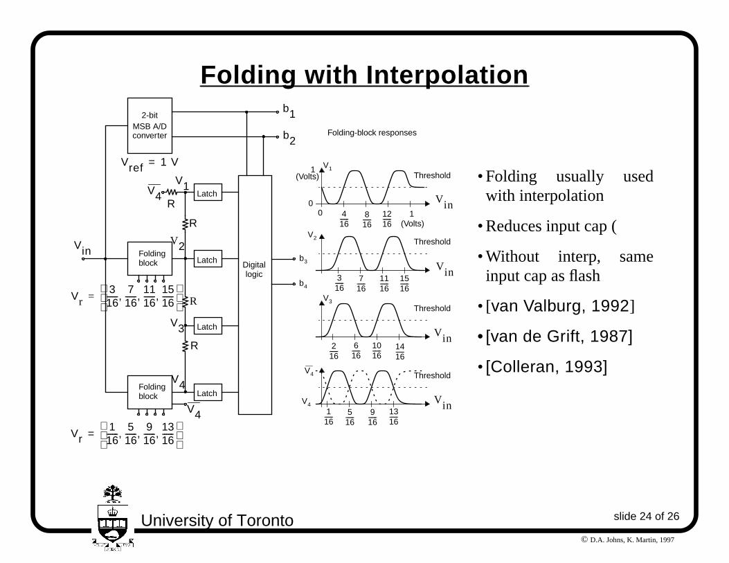
Folding with Interpolation
Foldingblock
Foldingblock
2-bitMSB A/Dconverter
Latch
Latch
Latch
Latch
Digitallogic
Vin
b1
b2
b3
b4
V1
V2
V3
V4
Vin
V1
Vin
V2
Vin
V3
VinV4
Threshold
Threshold
Threshold
Threshold
Folding-block responses
1(Volts)
(Volts)
Vr316------
716------
1116------
1516------, , ,
=
Vref 1 V=
Vr1
16------
516------
916------
1316------, , ,
=
416------ 8
16------
1216------
100
316------ 7
16------
1116------
1516------
216------
616------
1016------ 14
16------
116------ 5
16------
916------
1316------
R
R
V4
V4
V4
R
R
• Folding usually usedwith interpolation
• Reduces input cap (
• Without interp, sameinput cap as flash
• [van Valburg, 1992]
• [van de Grift, 1987]
• [Colleran, 1993]

slide 25 of 26University of Toronto© D.A. Johns, K. Martin, 1997
Pipelined A/D Con ver ters
D1
Q1
DN-2
QN-1
DN
QN
D1
Q1D1
Q1
DN-2
QN-1
1-bitDAPRX
1-bitDAPRX
1-bitDAPRX
1-bitDAPRX
Vin
N–
1-b
it sh
ift r
egis
ter
Analog pipeline(DAPRX - digital approximator)
b1
b2
bN
bN 1–
S/H
2
Cmp
–Vref/4
Vref/4
Vi–1
Vi
bi

slide 26 of 26University of Toronto© D.A. Johns, K. Martin, 1997
Time-Interlea ved A/D Con ver ters [Blac k, 80]
• Use parallel A/Ds and multiplex them• Tone occurs at fs/N for N converters if mismatched• Input S/H critical, others not — perhaps different tech for input S/H
S/H
S/H
S/H
S/H
S/H
N-bit A/D
N-bit A/D
N-bit A/D
N-bit A/D
Dig.mux
Digitaloutput
f2
f3
f4
f1
f0
Vin