model mn4783a test set for the me7840/4 handset amplifier …
TRANSCRIPT

P/N: 10410-00248REVISION: A
PRINTED: OCTOBER 2003COPYRIGHT 2003 ANRITSU CO.
MODEL MN4783A TEST SETFOR THE
ME7840/4 HANDSET AMPLIFIER TEST SYSTEM
MAINTENANCE MANUAL
490 JARVIS DRIVE l MORGAN HILL, CA 95037-2809

WARRANTY
The Anritsu product(s) listed on the title page is (are) warranted against defects in materials andworkmanship for three years from the date of shipment.Anritsu’s obligation covers repairing or replacing products which prove to be defective during thewarranty period. Buyers shall prepay transportation charges for equipment returned to Anritsu forwarranty repairs. Obligation is limited to the original purchaser. Anritsu is not liable for consequen-tial damages.
LIMITATION OF WARRANTY
The foregoing warranty does not apply to Anritsu connectors that have failed due to normal wear.Also, the warranty does not apply to defects resulting from improper or inadequate maintenance bythe Buyer, unauthorized modification or misuse, or operation outside of the environmental specifica-tions of the product. No other warranty is expressed or implied, and the remedies provided hereinare the Buyer’s sole and exclusive remedies.
TRADEMARK ACKNOWLEDGEMENTS
Scorpion and Scorpion Navigator are registered trademarks of Anritsu Company.Windows is a registered trademark of Microsoft Corporation.
NOTICE
Anritsu Company has prepared this manual for use by Anritsu Company personnel and customersas a guide for the proper installation, operation and maintenance of Anritsu Company equipmentand computer programs. The drawings, specifications, and information contained herein are theproperty of Anritsu Company, and any unauthorized use or disclosure of these drawings, specifica-tions, and information is prohibited; they shall not be reproduced, copied, or used in whole or in partas the basis for manufacture or sale of the equipment or software programs without the prior writ-ten consent of Anritsu Company.

Safety Symbols
To prevent the risk of personal injury or loss related to equipmentmalfunction, ANRITSU Company uses the following symbols to indi-cate safety-related information. For your own safety, please read thisinformation carefully BEFORE operating the equipment.
Symbols used in manuals
DANGER Indicates a very dangerous procedure that could result in serious in-jury or death if not performed properly.
WARNING Indicates a hazardous procedure that could result in serious injury ordeath if not performed properly.
CAUTION Indicates a hazardous procedure or danger that could result in light-to-severe injury, or loss related to equipment malfunction, if properprecautions are not taken.
Safety Symbols Used on Equipment and in Manuals
Some or all of the following five symbols may or may not be used on all ANRITSU equipment. In addition,there may be other labels attached to products that are not shown in the diagrams in this manual.
The following safety symbols are used inside or on the equipment nearoperation locations to provide information about safety items and op-eration precautions. Ensure that you clearly understand the meaningsof the symbols and take the necessary precautions BEFORE operatingthe equipment.
This symbol indicates a prohibited operation. The prohibited operationis indicated symbolically in or near the barred circle.
This symbol indicates a compulsory safety precaution. The requiredoperation is indicated symbolically in or near the circle.
This symbol indicates warning or caution. The contents are indicatedsymbolically in or near the triangle.
This symbol indicates a note. The contents are described in the box.
These symbols indicate that the marked part should be recycled.
MN4783A MM Safety-1

Safety-2 MN4783A MM
When supplying AC power to this equipment, connect the accessory 3-pin power cord to a 3-pin grounded power outlet. If a grounded 3-pinoutlet is not available, use a conversion adapter and ground the greenwire, or connect the frame ground on the rear panel of the equipmentto ground. If power is supplied without grounding the equipment, thereis a risk of receiving a severe or fatal electric shock.
WARNING
This equipment cannot be repaired by the operator. DO NOT attempt toremove the equipment covers or to disassemble internal components.Only qualified service technicians with a knowledge of electrical fireand shock hazards should service this equipment. There are high-voltage parts in this equipment presenting a risk of severe injury or fa-tal electric shock to untrained personnel. In addition, there is a risk ofdamage to precision components.
WARNING
WARNING
Repair
For Safety
WARNING
Always refer to the operation manual when working near locations atwhich the alert mark, shown on the left, is attached. If the operation,etc., is performed without heeding the advice in the operation manual,there is a risk of personal injury. In addition, the equipment perform-ance may be reduced.
Moreover, this alert mark is sometimes used with other marks and de-scriptions indicating other dangers.
If this equipment is used in a manner not specified by the manufac-turer, the protection provided by the equipment may be impaired.
WARNING

Table of Contents, Narrative
Chapter 1 — General Service InformationThis chapter provides a general description of the Model MN4783A Test Set for the ME7840/4 PowerAmplifier Test System, Handset Configuration. It explains the level of maintenance covered in thismanual and the service strategy used throughout this manual. It also contains static-sensitive com-ponent handling precautions and a list of recommended test equipment.
Chapter 2 — Replaceable PartsThis chapter lists all replaceable subassemblies and components for the MN4783A model. It explainsthe Anritsu exchange assembly program and provides parts ordering information.
Chapter 3 — Performance Verification ProceduresThis chapter provides detailed procedures for verifying that the performance of the MN4783A meetsthe minimum performance standards.
Chapter 4 — TroubleshootingThis chapter provides information for troubleshooting the MN4783A Test Set. The troubleshootingprocedures contained in this chapter support fault isolation down to a replaceable subassembly.
Chapter 5 — Removal and Replacement ProceduresThis chapter describes how to gain access to all of the major assemblies and major parts for trouble-shooting and/or replacement.
Appendix A — Connector Maintenance Check ProceduresThis appendix contains procedures and information needed to perform maintenance checks (includ-ing pin-depth measurements) for the connectors on all Anritsu supplied Calibration/Verification Kitcomponents, Through-cables, and other associated RF/microwave components.
Index
MN4783A MM i

Table of ContentsChapter 1 General Information
1-1 SCOPE OF MANUAL . . . . . . . . . . . . . . . . . . . . . . . . . . . . . . . . . 1-1
1-2 INTRODUCTION . . . . . . . . . . . . . . . . . . . . . . . . . . . . . . . . . . . 1-1
1-3 RELATED MANUALS. . . . . . . . . . . . . . . . . . . . . . . . . . . . . . . . . 1-1
1-4 IDENTIFICATION NUMBER. . . . . . . . . . . . . . . . . . . . . . . . . . . . . 1-2
1-5 CONVENTIONS . . . . . . . . . . . . . . . . . . . . . . . . . . . . . . . . . . . . 1-2
1-6 SYSTEM OVERVIEW . . . . . . . . . . . . . . . . . . . . . . . . . . . . . . . . . 1-2
1-7 HARDWARE DESCRIPTION . . . . . . . . . . . . . . . . . . . . . . . . . . . . . 1-2
1-8 SYSTEM DESCRIPTION . . . . . . . . . . . . . . . . . . . . . . . . . . . . . . . 1-4
DRA Scorpion · · · · · · · · · · · · · · · · · · · · · · · · · · · · · · · · · · · 1-4MN4783A Test Set· · · · · · · · · · · · · · · · · · · · · · · · · · · · · · · · · 1-5Connectors and Ports · · · · · · · · · · · · · · · · · · · · · · · · · · · · · · · 1-6
1-9 SERVICE CENTERS . . . . . . . . . . . . . . . . . . . . . . . . . . . . . . . . . 1-8
1-10 STATIC SENSITIVE COMPONENT HANDLING PROCEDURES. . . . . . . . . 1-8
1-11 RECOMMENDED TEST EQUIPMENT . . . . . . . . . . . . . . . . . . . . . . . 1-8
Chapter 2 Replaceable Parts2-1 INTRODUCTION . . . . . . . . . . . . . . . . . . . . . . . . . . . . . . . . . . . 2-1
2-2 EXCHANGE ASSEMBLY PROGRAM . . . . . . . . . . . . . . . . . . . . . . . . 2-1
2-3 REPLACEABLE SUBASSEMBLIES AND PARTS . . . . . . . . . . . . . . . . . 2-2
2-4 PARTS ORDERING INFORMATION . . . . . . . . . . . . . . . . . . . . . . . . 2-2
Chapter 3 Performance Verification Procedure3-1 INTRODUCTION . . . . . . . . . . . . . . . . . . . . . . . . . . . . . . . . . . . 3-1
3-2 CONVENTIONS . . . . . . . . . . . . . . . . . . . . . . . . . . . . . . . . . . . . 3-1
3-3 SOURCE OUTPUT ACCURACY . . . . . . . . . . . . . . . . . . . . . . . . . . . 3-2
3-4 DIRECTIVITY AND TEST PORT MATCH. . . . . . . . . . . . . . . . . . . . . . 3-4
3-5 SYSTEM DYNAMIC RANGE . . . . . . . . . . . . . . . . . . . . . . . . . . . . . 3-7
ii MN4783A MM

Chapter 4 Troubleshooting4-1 INTRODUCTION . . . . . . . . . . . . . . . . . . . . . . . . . . . . . . . . . . . 4-1
4-2 TROUBLESHOOTING . . . . . . . . . . . . . . . . . . . . . . . . . . . . . . . . 4-1
Power Up Failure · · · · · · · · · · · · · · · · · · · · · · · · · · · · · · · · · 4-2Directivity and Test Port Match Failure · · · · · · · · · · · · · · · · · · · · · 4-4Dynamic Range Failure · · · · · · · · · · · · · · · · · · · · · · · · · · · · · · 4-5
4-3 OPERATIONAL CHECK . . . . . . . . . . . . . . . . . . . . . . . . . . . . . . . 4-5
4-4 COMBINER CHECK . . . . . . . . . . . . . . . . . . . . . . . . . . . . . . . . . 4-6
4-5 PORT MODULE CHECK . . . . . . . . . . . . . . . . . . . . . . . . . . . . . . 4-10
4-6 TEST CHANNEL STEP ATTENUATOR CHECK . . . . . . . . . . . . . . . . . 4-14
Chapter 5 Removal and Replacement Procedures5-1 INTRODUCTION . . . . . . . . . . . . . . . . . . . . . . . . . . . . . . . . . . . 5-1
5-2 EQUIPMENT REQUIRED . . . . . . . . . . . . . . . . . . . . . . . . . . . . . . 5-1
5-3 REMOVING THE COVERS . . . . . . . . . . . . . . . . . . . . . . . . . . . . . . 5-1
5-4 CONTROL PCB . . . . . . . . . . . . . . . . . . . . . . . . . . . . . . . . . . . . 5-4
5-5 RF AMPLIFIERS . . . . . . . . . . . . . . . . . . . . . . . . . . . . . . . . . . . 5-5
5-6 STEP ATTENUATOR . . . . . . . . . . . . . . . . . . . . . . . . . . . . . . . . . 5-6
5-7 POWER DIVIDERS . . . . . . . . . . . . . . . . . . . . . . . . . . . . . . . . . . 5-7
5-8 POWER SUPPLY . . . . . . . . . . . . . . . . . . . . . . . . . . . . . . . . . . . 5-8
5-9 RF SWITCHES . . . . . . . . . . . . . . . . . . . . . . . . . . . . . . . . . . . . 5-10
5-10 PORT MODULES . . . . . . . . . . . . . . . . . . . . . . . . . . . . . . . . . . 5-12
5-11 FAN ASSEMBLY . . . . . . . . . . . . . . . . . . . . . . . . . . . . . . . . . . . 5-13
MN4783A MM iii
Table of Contents (Continued)

Appendix A Connector Maintenance Check ProceduresA-1 INTRODUCTION . . . . . . . . . . . . . . . . . . . . . . . . . . . . . . . . . . . A-1
A-2 PRECAUTIONS . . . . . . . . . . . . . . . . . . . . . . . . . . . . . . . . . . . . A-1
Pin Depth Problems · · · · · · · · · · · · · · · · · · · · · · · · · · · · · · · · A-1Pin-Depth Tolerance · · · · · · · · · · · · · · · · · · · · · · · · · · · · · · · A-2Avoid Over Torquing Connectors · · · · · · · · · · · · · · · · · · · · · · · · · A-3Teflon Tuning Washers · · · · · · · · · · · · · · · · · · · · · · · · · · · · · · A-3Avoid Mechanical Shock · · · · · · · · · · · · · · · · · · · · · · · · · · · · · A-3Keep Connectors Clean · · · · · · · · · · · · · · · · · · · · · · · · · · · · · · A-3Visual Inspection · · · · · · · · · · · · · · · · · · · · · · · · · · · · · · · · · A-3
A-3 REPAIR/MAINTENANCE . . . . . . . . . . . . . . . . . . . . . . . . . . . . . . A-3
Index
iv MN4783A MM
Table of Contents (Continued)
Chapter 1General Information
1-1 SCOPE OF MANUAL This manual provides general service and preventive maintenance in-formation for the Anritsu MN4783A test set for the ME7840/4 PowerAmplifier Test System, Handset Configuration. It contains proceduresfor:
� Testing the instrument for proper operation
� Verifying measurement accuracy and traceability to the NationalInstitute of Standards and Technology (NIST)
� Troubleshooting a failed instrument to the exchange subassem-bly level or to the subsystem requiring adjustment
� Locating and replacing failed parts
The procedures described in this manual presume a working knowl-edge of vector network analyzers and RF power amplifier testing pro-cedures. Refer to the other manuals supplied with the ME7840/4 testsystem for more detailed explanations of the system equipment andprocedures.
1-2 INTRODUCTION This chapter provides a general description of the power amplifier testsystem’s identification numbers, frequency ranges, and related manu-als. It also includes service strategy, available service facilities,static-sensitive component handling precautions, and a list of recom-mended test equipment.
1-3 RELATED MANUALS The ME7840/4 manual set consists of the following manuals:
Manual Description Anritsu Part Number
ME7840/4 Operation Manual (OM) 10410-00247
MN4783A Maintenance Manual (MM) 10410-00248 (optional)
Scorpion Navigator User’s Guide (SUG) 10410-00249
MS462XX Operating Manual (OM) 10410-00203
MS462XX Programming Manual (PM) 10410-00204
MS462XX Maintenance Manual (MM) 10410-00205 (optional)
The operating and programming manuals are supplied with the equip-ment; the maintenance manuals are optional items that may be pur-chased.
MN4783A MM 1-1

1-4 IDENTIFICATIONNUMBER
All Anritsu instruments are assigned a six-digit ID number, such as“030101.” This number appears on a decal affixed to the rear panel.Please use this identification number during any correspondence withAnritsu Customer Service about this instrument.
1-5 CONVENTIONS Throughout this manual, the ME7840/4 Power Amplifier Test System,Handset Configuration may be referenced as ME7840/4, or test sys-tem; the MS462XC Vector Network Measurement System may be ref-erenced as VNMS, Scorpion or MS462XC; the MN4783A test set maybe referenced as test set or MN4783A; the Amplifier Under Test, in-cluding the related components to their system, may be referenced asAUT.
1-6 SYSTEM OVERVIEW The Anritsu ME7840/4 is intended for the measurement and real-timegraphical display of the following parameters of a power amplifier inthe frequency range of 10 MHz to 6 GHz:
� S-parameters including Hot S22 and K-factor
� Single-tone Power Sweep
� Two-tone Power Sweep
� Intermodulation Distortion
� Harmonics
� Noise Figure
� Adjacent Channel Power Ratio (ACPR)
The ME7840/4 test system is designed to facilitate alignment, tuningand pass/fail testing of the components, modules, and subassemblies ofRF and microwave power amplifiers as well as the assembled ampli-fier systems.
1-7 HARDWAREDESCRIPTION
The ME7840/4 hardware consists of a MS462XC Direct Receiver Ac-cess (DRA) Scorpion®, a MN4783A test set, a customer supplied Per-sonal Computer (PC), and an optional current probe. A block diagramof the ME7840/4 test system is shown in Figure 1-1 on the followingpage. General test set specifications appear below:
IDENTIFICATION NUMBER GENERAL INFORMATION
1-2 MN4783A MM
ModelFrequency Range
(MHz)Maximum AUT Power
Output (Watts)Reverse Measurements
(S22, Hot S22, S12 Possible)Attenuator or Isolator(at AUT Output Path)
MN4783A 10 to 6000(Note 1)
5.0(Note 2)
Yes External
Notes:1. The frequency range does not account for any restricting effects caused by use of external isolators or circulators.2. The maximum AUT power assumes a minimum isolation of 20 dB provided by external isolators or circulators. The provided exter-nal 20 dB attenuator ensures the proper isolation for reverse measurements up to the specified maximum AUT power output.
Table 1-1. Test Set Configuration

GENERAL INFORMATION HARDWARE DESCRIPTION
MN4783A MM 1-3
OPTIONALPOWER METER
OPTIONAL SPECTRUMANALYZER
SYSTEM CONTROLLER(PC)GPIB BUS
B2
DUT
Port1Port3 B1A1 A2
STEPATTEN
HATSTESTSET
Port2
OPTIONALMODULATIONSYNTHESIZER
SOURCE 1
SOURCE 2
TRANSFERSW
SPDTSW
DOWNCONVERSION
MODULE
ALC
ARM
ALC
PORT 3MODULE
MS4623C withOptions
3D, 4E, 8, 13, 24
LO
IF IF
+10dBm
+10dBm
+10dBm
23dBm
18.8dBm
15 dBmmax -15
dBm37dBm [5W]
Max.
-20dB
-20dB
-20dB
17 dBm
D29830
J1J2J3J4
JTJR
OptionalExternal
PRE-AMP
J5
J3
NN N N
N NN
K
S
-20dB
J2
J4
J1
J2
(P3)
J3
J1
1 2
0
N N N
NoiseIn
+8 dBm
PWRDIVIDER
Amp
23dBm
19.5 dBm
20dB10WPad
SSSS S S
SW3
13.5dBm
K
S
SS S S
SW1
SW2
NoiseOut
10 dB10 dB
0 - 70 dB
Control In
D-Sub 15
8-bit TTLControl Line
Ext Loop
SW Driver/DC powerRegulator/
ControlPCB
8-bit TTL
bits0-2
bit3
bit4
PWRCOMBINER
K Noise In
Noise+28V
NoiseSource
BNC
C1 C2A1 B1 B2 A2
Input OutputExt.Source
Test Port 1 Test Port 2 Aux.Out
+8/-5v+8/-5v
optionalisolator
toPort1
toPort3
toPort2
OPTIONAL POWERSUPPLY / SOURCE
METER
Ext I/O
D-Sub 15
Figure 1-1. Overall Functional Block Diagram of the ME7840/4 Power Amplifier Test System, Handset Configurationwith the MN4783A Test Set.

1-8 SYSTEM DESCRIPTION The ME7840/4 test system consists of the MS462XC Direct ReceiverAccess Scorpion (DRA), the MN4783A Handset Amplifier Test Set anda library of external measurement software. Scorpion Navigator® or-chestrates the calibration and performs measurements on power am-plifiers in the 10 MHz to 6 GHz range. Software modules exist forS-parameters, K-factor, IMD, One-Tone Power Sweep, Two-Tone PowerSweep, Harmonics, Hot S22, Noise Figure, and ACPR measurements.Scorpion Navigator software runs best on Windows® NT/2000/XP andrequires a GPIB controller (preferably a National Instruments GPIBcontroller with NI-488.2 software version 1.7 or higher and NI VISAversion 2.5 or higher) and Scorpion firmware version 1.11 or higher.
DRA Scorpion The Scorpion Direct Receiver Access version of the Vector NetworkMeasurement System functions under control of the software residingin the PC through GPIB commands. The software supports tuning andalignment operations by generating real time graphic displays of themeasured data on the PC screen.
Under software control, 3rd, 5th, 7th, and 9th order IMD products can bemeasured and displayed. Also, the Upper and Lower Side Band (USBand LSB) components of the IMD products are measured anddisplayed separately.
The DRA Scorpion includes the following capabilities:
� Two internal, independent RF sources. Each source has a rangeof –15 dBm to +10 dBm. A 0 dB to 70 dB step attenuator (10 dB /step) is provided for each source resulting in a power outputrange of –85 dBm to +10 dBm from each source.
� Complete built-in capability for IMD measurements. A combineris provided in the test set.
� Internal Transfer Switch enabling S22 and Hot S22 measure-ments. The reflectometer set-up is provided in the test set.
� Direct access to each of the four receiver channels (two referencechannels and two test channels) for maximum flexibility in mea-suring forward and reverse S-parameters over a wide range ofAUT output power. The test set provides incident and reflectedsignal separation.
SYSTEM DESCRIPTION GENERAL INFORMATION
1-4 MN4783A MM
CAUTIONThe combiner has a power in-put rating of 5 Watts maxi-mum when terminated with aVSWR of 2:1. For an open orshort at the combiner output,the combiner input power rat-ing is 0.5 Watts maximum.

MN4783A Test Set The MN4783A test set contains a Wilkinson type combiner that com-bines the two RF signals from Port 1 and Port 3 (RF1 and RF3) of theScorpion. Two preamplifiers at the combiner input boost the input RFpower to the AUT.
The output of the combiner is fed to source selection switches that en-able one of the following to be applied to the AUT:
� The combined signal from the Scorpion sources
� A modulated signal from an optional external modulation synthe-sizer
� An innovative noise figure measurement capability based onY-factor techniques that can be routed through the test set foruse in characterizing amplifiers
A provision for the insertion of an optional external preamplifier (afterthe combiner and source selection switch) is also provided.
The test set includes two VSWR bridges (Port Modules) connectedback-to-back at the input of the AUT that separates the incident sig-nal from the reflected signal. The power rating of these VSWR bridgesis 5 Watts average. The –20 dB portion of the incident and reflectedsignals are applied to the Scorpion reference-port a1 and test-port b1,respectively, for S11 measurement. The S11 measurement determined bythe DRA Scorpion is simply the ratio of the reflected signal to the inci-dent signal.
The amplified output of the AUT is fed to a VSWR bridge in the testset. The power rating of this bridge is also 5 Watts average. The–20 dB coupled arm of this bridge is routed to the test-port b2 of theScorpion through a Wilkinson type power divider and a 0 dB to 70 dBstep attenuator (10 dB/step).
The divider enables the connections of a power meter or spectrum ana-lyzer, when desired, to measure the AUT output using the AUX OUTconnector. The through arm of the bridge is routed to the ScorpionPort 2 via a 20 dB 10 Watt attenuator (or optional isolator).
In the MN4783A test set, the attenuator (or isolator) is external. In se-lecting an external isolator (alternatively, a circulator with a termina-tion on the unused port may be used), the following criteria should befollowed:
� Power rating: Should be no less than the power output of theAUT
� Bandwidth: Should be sufficiently wide to cover the frequencyband of the AUT
� Isolation: Should be no less than (Po �17 dB), where Po is thepower output in dBm of the AUT
GENERAL INFORMATION SYSTEM DESCRIPTION
MN4783A MM 1-5

Where S22 or Hot S22 measurements are not required, power amplifierswith up to 5 Watts average output power can be tested with theMN4783A test set without any isolator by connecting the 20 dB10 Watt attenuator to port C1 and port C2 on the rear panel. The unitis shipped from the factory with this attenuator in place.
For S22 measurements, the transfer switch located within the Scorpionroutes the Source 1 output signal to the output port of the AUT viaPort 2 (RF2) of the Scorpion. A separate VSWR bridge in the test setapplies the –20 dB portion of this incident signal to the Scorpion refer-ence-port a2. The –20 dB portion of the signal reflected from the AUToutput port is applied to the Scorpion test-port b2 by means of the AUToutput VSWR bridge.
The ME7840/4 calibration is performed with the test set in place andat the connectors where the AUT will be connected directly. Therefore,the test set components and cables are included in the calibration loopand their effects are calibrated out, resulting in correct and accuratemeasurements of the AUT.
The software supplied by Anritsu supports operator control of thesource selection switch and step attenuator in the test set. This controlis achieved through the parallel TTL control lines available at theScorpion rear panel “External I/O” connector. The GPIB commandsfrom the PC to the Scorpion set the TTL control lines to the desiredstates.
Connectors and Ports On the front panel of the model MS462XC DRA Scorpion, three type N(female) connectors are provided for Ports 1, 2 and 3.
Port 1 provides RF Source 1 when the transfer switch is in the forwardposition, and is terminated into 50 ohms to ground when the transferswitch is in the reverse position.
Port 2 provides RF Source 1 when the transfer switch is in the reverseposition, and is terminated into 50 ohms to ground when the transferswitch is in the forward position.
Port 3 is allocated to RF Source 2. Under independent control, Port 3provides RF Source 2 or is terminated into 50 ohms to ground.
On the rear panel of the Scorpion, four SMA connectors are providedfor reference ports (a1 and a2) and test ports (b1 and b2). On theMN4783A test set, two additional SMA connectors provide for connect-ing an external isolator. If reverse measurements (S22 and Hot S22) arenot desired, then an isolator is not required. Instead, a 20 dB externalattenuator should be connected between connectors C1 and C2. TheMN4783A is shipped from the factory with this attenuator in place.
SYSTEM DESCRIPTION GENERAL INFORMATION
1-6 MN4783A MM
CAUTIONConnecting the externalcirculator incorrectly orplacing a direct connectionbetween C1 and C2 on theMN4783A rear panel willcause permanent damageto the MS462XC.
The unused port of thecirculator must be termi-nated with a high powertermination.

GENERAL INFORMATION SYSTEM DESCRIPTION
MN4783A MM 1-7
NoiseIn
Noise+28V
NO OPERATOR SERVICE-ABLE PARTS INSIDE.REFER SERVICING TOQUALIFIED PERSONNEL.
WARNING
CAUTIONFOR CONTINUED FIREPROTECTION REPLACEONLY WITH SPECIFIEDTYPE AND RATED FUSE.
IEEE 488.2GPIB
DedicatedGPIB
Serial Port Ethernet VGA SCSI-2
ExtAnalogOutput
ExtTrigger
LPT Line Printer Ext I/O
Ext AnalogIn
ExtSource
Ext 10 MHzIn
47-440 Hz85-264VAC
REPLACE FUSE ONLY WITHSAME TYPE AND RATING
CAUTIONDO NOT OPERATE
WITH POWER CORDUNGROUNDED
N274
a1 b1 b2a2
Figure 1-2. MS462XC Rear Panel Drawing
Figure 1-3. MN4783A Rear Panel Drawing

1-9 SERVICE CENTERS Anritsu Company offers a full range of repair and calibration servicesat fully staffed and equipped service centers throughout the world. Ta-ble 1-3, located on page 1-10, lists all Anritsu services centers.
1-10 STATIC SENSITIVECOMPONENTHANDLINGPROCEDURES
The test set contains components that can be damaged by static elec-tricity. Figure 1-2 illustrates the precautions that should be followedwhen handling static-sensitive subassemblies and components. If fol-lowed, these precautions will minimize the possibilities of static-shockdamage to these items.
1-11 RECOMMENDED TESTEQUIPMENT
Table 1-2 lists the recommended test equipment to be used for allmaintenance activities for the MN4783A test set. Note the “Use”codes listed in the right hand column of the table. These codes list theapplicable maintenance activities for the equipment listed.
1-8 MN4783A MM
SERVICE CENTERS GENERAL INFORMATION
INSTRUMENTCRITICAL
SPECIFICATIONRECOMMENDED
MANUFACTURER/MODELUSE**
Power Meter Anritsu ML2437A or MS2438A P
Power Sensor Anritsu MA2472A P
GPIB Cable IEEE 488-2 compliant Anritsu 2100-2, or equivalent P
Offset Termination 20 dB Return Loss Anritsu 29A50-20 P
Termination Return Loss 35 dB, DC to 3 GHz Anritsu 28L50LF OT
Adapter Anritsu 34NFNF50Anritsu 34SFSF50Anritsu 34NKF50
O, T
Air Line Anritsu 18N50 orAnritsu SC3833
P
Thru Line Anritsu 3670NN50-2 or15NN50-0.6B
P
Thru Line Phase stableLength: 4 feet (2 each)
GORE PhaseFlexTM
Part number EJD01D010480O, T
Calibration Kit Anritsu 3653 or 3753LF P,O
�� USE CODES:A Adjustment / Internal Hardware CalibrationO Operational TestingP Performance VerificationT Troubleshooting
Table 1-2. Recommended Test Equipment

GENERAL INFORMATION RECOMMENDED TEST EQUIPMENT
MN4783A MM 1-9
1. Do not touch exposed contacts onany static sensitive component.
2. Do not slide static sensitive compo-nent across any surface.
3. Do not handle static sensitive com-ponents in areas where the floor orwork surface covering is capable ofgenerating a static charge.
4. Wear a static-discharge wristbandwhen working with static sensitivecomponents.
5. Label all static sensitive devices. 6. Keep component leads shorted to-gether whenever possible.
7. Handle PCBs only by their edges.Do not handle by the edge connec-tors.
8. Lift & handle solid state devices bytheir bodies – never by their leads.
9. Transport and store PCBs andother static sensitive devices instatic-shielded containers.
10. ADDITIONAL PRECAUTIONS:� Keep work spaces clean and free of any objects capable of holding or storing a static charge.� Connect soldering tools to an earth ground.� Use only special anti-static suction or wick-type desoldering tools.
Figure 1-4. Static Sensitive Component Handling Procedures

RECOMMENDED TEST EQUIPMENT GENERAL INFORMATION
1-10 MN4783A MM
UNITED STATESANRITSU COMPANY490 Jarvis DriveMorgan Hill, CA 95037-2809Telephone: (408) 776-83001-800-ANRITSUFAX: 408-776-1744
FRANCEANRITSU S.A9 Avenue du QuebecZone de Courtaboeuf91951 Les Ulis CedexTelephone: 016-09-21-550FAX: 016-44-61-065
JAPANANRITSU CUSTOMER SERVICE LTD.1800 Onna Atsugi-shiKanagawa-Prf. 243 JapanTelephone: 0462-96-6688FAX: 0462-25-8379
ANRITSU COMPANY10 New Maple Ave., Unit 305Pine Brook, NJ 07058Telephone: (973) 227-89991-800-ANRITSUFAX: 973-575-0092
GERMANYANRITSU GmbHGrafenberger Allee 54-56D-40237 Dusseldorf, GermanyTelephone: 0211-968550FAX: 0211-9685555
SINGAPOREANRITSU (SINGAPORE) PTE LTD.10, Hoe Chiang Road#07-01/02 Keppel TowersSingapore 089315Telephone: 282-2400FAX: 282-2533
ANRITSU COMPANY1155 E. Collins BlvdRichardson, TX 75081Telephone: 1-800-ANRITSUFAX: 972-671-1877
INDIAMEERA AGENCIES PVT. LTD.23 Community CentreZamroodpur, Kailash Colony Extension,New Delhi, India 110 048Phone: 011-2-6442700/6442800FAX : 011-2-644250023
SOUTH AFRICAETECSA12 Surrey Square Office Park330 Surrey AvenueFerndale, Randburt, 2194South AfricaTelephone: 011-27-11-787-7200FAX: 011-27-11-787-0446
AUSTRALIAANRITSU PTY. LTD.Unit 3, 170 Foster RoadMt Waverley, VIC 3149AustraliaTelephone: 03-9558-8177FAX: 03-9558-8255
ISRAELTECH-CENT, LTD.4 Raul Valenberg StTel-Aviv 69719Telephone: (03) 64-78-563FAX: (03) 64-78-334
SWEDENANRITSU ABBotivid CenterFittja Backe 13A145 84 StockholmnTelephone: (08) 534-707-00FAX: (08) 534-707-30
BRAZILANRITSU ELECTRONICA LTDA.Praia de Botafogo, 440, Sala 2401CEP22250-040, Rio de Janeiro, RJ, BrasilTelephone: 021-527-6922FAX: 021-53-71-456
ITALYANRITSU Sp.ARoma OfficeVia E. Vittorini, 12900144 Roma EURTelephone: (06) 50-99-711FAX: (06) 50-22-4252
TAIWANANRITSU CO., INC.7F, No. 316, Section 1NeiHu RoadTaipei, Taiwan, R.O.C.Telephone: 886-2-8751-1816FAX: 886-2-8751-2126
CANADAANRITSU INSTRUMENTS LTD.700 Silver Seven Road, Suite 120Kanata, Ontario K2V 1C3Telephone: (613) 591-2003FAX: (613) 591-1006
KOREAANRITSU CORPORATION LTD.Head Office:14F, Hyunjuk Building 832-41Yeoksam-Dong, Kangnam-KuSeoul 135-080, South KoreaTelephone: 02-553-6603FAX: 02-553-6604
Service Center:8F Hyunjuk Building832-41, Yeoksam DongKangnam-GuSeoul, South Korea 135-080Telephone: 82-2-553-6603FAX: 82-2-553-6605
UNITED KINGDOMANRITSU LTD.200 Capability GreenLuton, BedfordshireLU1 3LU, EnglandTelephone: 015-82-433200FAX: 015-82-731303
CHINAANRITSU ELECTRONICS (SHANGHAI) CO. LTD.2F, Rm B, 52 Section Factory BuildingNo. 516 Fu Te Rd (N)Shanghai 200131 P.R. ChinaTelephone:21-58680226, 58680227, 58680228FAX: 21-58680588
Table 1-3. Anritsu Service Centers

Chapter 2Replaceable Parts
2-1 INTRODUCTION This chapter provides replaceable parts information for bothMN4783A models. The major replaceable test set assemblies and partsare listed in Table 2-1. The locations of these assemblies/parts areshown in Figure 2-1.
2-2 EXCHANGE ASSEMBLYPROGRAM
Anritsu maintains a module exchange program for selected subassem-blies. If a malfunction occurs in one of these subassemblies, the defec-tive item can be exchanged. Upon receiving your request, Anritsu willship the exchange subassembly to you, typically within 24 hours. Youthen have 45 days in which to return the defective item. All exchangesubassemblies or RF assemblies are warranted for 90 days from thedate of shipment, or for the balance of the original equipment war-ranty, whichever is longer.
NOTEWhen sending a failed assembly to the factory for exchange,acopy of the Service Log must always accompany the failedassembly. This copy may be a printout, or a saved disk copy.Due to the importance of the service log information to theAnritsu factory Service Engineers, the exchange prices areonly valid if the service log data is included with the failedassembly.
Please have the exact model number and serial number of your unitavailable when requesting this service, as the information about yourunit is filed according to the instrument’s model and serial number.For more information about the program, contact your local sales rep-resentative or call Anritsu Customer Service direct (refer toSection 2-4.
MN4783A MM 2-1

2-3 REPLACEABLESUBASSEMBLIES ANDPARTS
Table 2-1 lists the major replaceable subassemblies and parts for theMN4783A. These assemblies/parts are presently covered by theAnritsu exchange assembly program.
2-4 PARTS ORDERINGINFORMATION
All of the parts listed in Table 2-1 may be ordered from your localAnritsu service center (Table 1-3, page 1-10). Or, they may be ordereddirectly from the factory at the following address:
Anritsu CompanyATTN: Customer Service490 Jarvis DriveMorgan Hill, CA 95037-2809
Telephone: (408)-778-2000FAX: (408)-778-0239
REPLACEABLE SUBASSEMBLIES AND PARTS REPLACEABLE PARTS
2-2 MN4783A MM
Part Number Description
1010-49 20 dB Fixed Attenuator, 10 Watt
43KB-10 10 dB Fixed Attenuator
40-160 Power Supply
60547-3 Control PCB Assembly
61603 Combiner/Power Divider, 500 MHz to 6 GHz
ND60348 Amplifier 1 with Cable Harness
ND60349 Amplifier 2 with Cable Harness
ND60721 Switch 1 with Cable Harness
ND60722 Switch 2 with Cable Harness
ND60723 Switch 3 with Cable Harness
ND60327 Fan Assembly
339H40998A Step Attenuator
46720 Port 1 and Port 2 Modules (VSWR Bridges)
B45259 N Female Test Port Connector
Table 2-1. Replaceable Subassemblies

REPLACEABLE PARTS PARTS ORDERING INFORMATION
MN4783A MM 2-3
Switch 1
Switch 2
Switch 3
Power Supply
Power Divider 2
Power Divider 1
Bridge 1
Bridge 3
Bridge 2
Bridge 4
AMP 1
AMP 2
Fan
JS
P
JS
P
JSP
JS
P
AT
TE
NU
AT
OR
JB
JB
JB
JB
Control PCB
Front
Figure 2-1. Major Assemblies Location Diagram (Top View)

PARTS ORDERING INFORMATION REPLACEABLE PARTS
2-4 MN4783A MM
Red Black
Blue
Brown
Green/Yellow
LED
Switch 1
Switch 2
Switch 3
Power Supply
Power Divider 2
Power Divider 1
Bridge 1
Bridge 3
Bridge 2
Bridge 4
AMP 1
AMP 2
Fan
JS
P
JS
P
JSP
JS
P
AT
TE
NU
AT
OR
JB
JB
JB
JB
Control PCB
Note: The Control PCB is shown face up for clarity.
Figure 2-2. Major Assemblies Wiring Diagram (Top View)
REPLACEABLE PARTS PARTS ORDERING INFORMATION
MN4783A MM 2-5
Input OutputTo Port 3
(Top)
Ext. Source
AUX Out
(Bottom)
To Port 1
(Top)
Test Port 1
To Port 2
(Top)
Test Port 2
(Bottom)
Control InB2 B1 A2 A1 C2 Noise
Source In
C1Noise
Out
Switch 1
Switch 2
Switch 3
Power Supply
Power Divider 2
Power Divider 1
Bridge 1
Bridge 3
Bridge 2
Bridge 4
AMP 1
AMP 2
Fan
JS
P
JS
P
JSP
JS
P
AT
TE
NU
AT
OR
JB
JB
JB
JB
Control PCB
In
1
2In
1
2
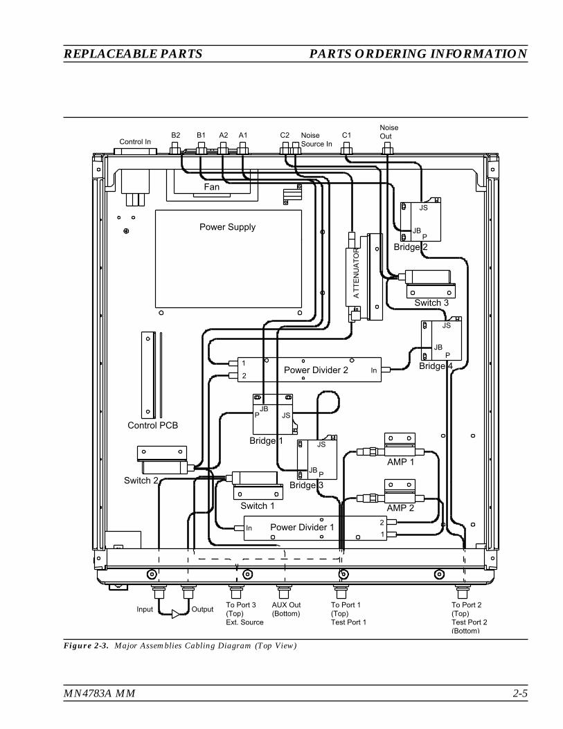
Figure 2-3. Major Assemblies Cabling Diagram (Top View)

PARTS ORDERING INFORMATION REPLACEABLE PARTS
2-6 MN4783A MM
Switch 2
Switch 1
Switch 3
AMP
Figure 2-4. Component Wiring Diagram

Chapter 3Performance VerificationProcedure
3-1 INTRODUCTION The following are the specific tests that should be used to verify theperformance of the Power Amplifier Test System ME7840 withOption 4 (ME7840/4):
� MS462XC Source Output Level Accuracy Test
� Directivity and Test Port Match Verification
� Dynamic Range Verification
3-2 CONVENTIONS The test instructions in this chapter will direct the use of front panelhard keys and soft keys. The hard keys and soft keys will appear in adifferent typeface. For example:
Step 1. Press the Utility key and select:
DIAGNOSTICSTROUBLESHOOTINGMOREVERIFY ALC CALIBRATION
The Utility key is a front panel hard key and DIAGNOSTICS, TROU-BLESHOOTING, MORE, and VERIFY ALC CALIBRATION are all softkeys.
MN4783A MM 3-1

3-3 SOURCE OUTPUTACCURACY
This test verifies the source output accuracy of the MS462XC. The testprocedure uses the built-in Power ALC Verification function of theMS462XC Basic Measurement software.
Required Equipment: The following equipment is required to perform the Source Output Ac-curacy verification procedure:
� Anritsu ML2437A/ML2438A Power Meter
� Anritsu MA2472A Power Sensor or equivalent
Setup: Set up the test equipment as described below:
Step 1. Connect a GPIB cable between the power meter GPIB connector andthe MS462XC dedicated GPIB connector, as shown in Figure 3-1.
Step 2. Turn on the MS462XC VNMS and allow it to warm-up for at least onehour.
SOURCE OUTPUT ACCURACY PERFORMANCE VERIFICATION
3-2 MN4783A MM
NoiseIn
Noise+28V
NO OPERATOR SERVICE-ABLE PARTS INSIDE.REFER SERVICING TOQUALIFIED PERSONNEL.
WARNING
CAUTIONFOR CONTINUED FIREPROTECTION REPLACEONLY WITH SPECIFIEDTYPE AND RATED FUSE.
IEEE 488.2GPIB
DedicatedGPIB
Serial Port Ethernet VGA SCSI-2
ExtAnalogOutput
ExtTrigger
LPT Line Printer Ext I/O
Port 1Port 2BiasBias
Port 2Bias Fuse
Port 1Bias Fuse
Ext AnalogIn
ExtSource
Ext 10 MHzIn
47-440 Hz85-264VAC
REPLACE FUSE ONLY WITHSAME TYPE AND RATING
CAUTIONDO NOT OPERATE
WITH POWER CORDUNGROUNDED
N274
00000001Made in UK
12-24V DC
(1.3A)
OUTPUT 1 OUTPUT 2 INPUT 1
DIGITAL
INPUT 2
ANALOG
CALIBRATORB
RS 232
PARALLEL PRINTER
GPIB / IEEE 488
CAUTION
DO NOT OPERATEWITH UNGROUNDEDPOWER CORD.
85-250 VAC
47-440Hz40VA MAX
SEE MANUAL FOR VOLTAGE RANGES ON BNC CONNECTORS
A
NO OPERATOR SERVICE-ABLE PARTS INSIDE.
WARNING
Figure 3-1. ML2430A Series Power Meter GPIB connection to the MS462XC Vector Network Measurement System

Test Procedure:
Step 1. Disconnect the interconnect cables between the output Port 1 of theMS462XC and the input Port 1 of the MN4782A test set and betweenthe output Port 3 of the MS462XC and the input Port 3 of theMN4783A test set.
Step 2. Press the Utility key and select:
DIAGNOSTICSTROUBLESHOOTINGMOREVERIFY ALC CALIBRATION
Step 3. Calibrate and zero the power sensor.
Step 4. Connect the power sensor to Port 1 of the MS462XC and select theSTART VERIFICATION soft key.
Step 5. Verify that Source 1 passes this test.
NOTEOnly the worst case test result will be displayed on the screenwhen the instrument fails this test. The failed test result isalso recorded in the Service Log.
Step 6. Press the SELECT SOURCE soft key to select Source 2.
Step 7. Connect the power sensor to Port 3 of the MS462XC and select theSTART VERIFICATION soft key.
Step 8. Verify that Source 2 passes this test.
CAUTIONThe TROUBLESHOOTING function must be properlyexited to restore normal measurement operation.
Step 9. Exit the TROUBLESHOOTING mode by selecting the menu soft keysas follows:
RETURNRETURNFINISHED, RECOVER FROM TROUBLESHOOTING
Step 10. Reconnect the interconnect cables between the output Port 1 of theMS462XC and the input Port 1 of the MN4783A test set and betweenthe output Port 3 of the MS462XC and the input Port 3 of theMN4783A test set.
PERFORMANCE VERIFICATION SOURCE OUTPUT ACCURACY
MN4783A MM 3-3

3-4 DIRECTIVITY AND TESTPORT MATCH
This procedure verifies that the corrected directivity (effectivedirectivity) and test port match (effective test port match) of the sys-tem meets specifications.
Required Equipment: The following equipment is required to perform the Directivity andTest Port Match verification procedure:
� Anritsu 3753LF or 3753R N Connector Calibration Kit
� Anritsu 18N50 or SC3833 Air Line
� Anritsu 29A50-20 Offset Termination
� Anritsu 22A50 Open/Short
Setup: Set up the test equipment as described below:
Step 1. Turn on the MS462XC VNMS and the MN4783A test set and allowthem to warm-up for at least one hour.
Step 2. Press the Default key, then the 0 key.
Step 3. Press the Seq key and select:
TTL I/OPARALLEL OUT SETUPSET PARALLEL OUT PORT (0-255)
Step 4. Change the value from 0 to 8 and Select:
RETURNRETURN
Step 5. Press the Display key and select:
DISPLAY MODESINGLE CHANNELRETURNGRAPH TYPELOG MAGNITUDE
DIRECTIVITY AND TEST PORT MATCH PERFORMANCE VERIFICATION
3-4 MN4783A MM

Test Procedure:
Step 1. If the calibration kit is an Anritsu Model 3753LF, insert the Calibra-tion Component Coefficients disk into the MS462XC floppy disk drive.For the Model 3753R calibration kit, skip to Step 3.
Step 2. Press the Cal key and select:
COMPONENT UTILITIESINSTALL KIT INFO FROM FLOPPY DISKRETURNPERFORM CAL 2 PORT
Step 3. Follow the prompts and select: (If skipped to step 3, what prompts?)
CAL METHOD: STANDARDLINE TYPE: COAXIALSELECT CALIBRATION TYPE: REFLECTION ONLY – PORT 1 ONLYFREQUENCY RANGE OF CALIBRATION: 10 MHz TO 6000 MHzSELECT CALIBRATION DATA POINTS: NORMALDATA POINTS: 401 POINTSPORT 1 CONNECTOR TYPE: N (F)LOAD TYPE: BROADBAND LOAD
Step 4. Select the START CAL soft key to begin the calibration.
Step 5. Install the calibration device per the instruction on the display and se-lect the appropriate soft key to measure the calibration device.
Step 6. When the message, “CALIBRATION SEQUENCE COMPLETED” is dis-played, press the Enter key to continue.
Step 7. Connect the N male connector end of the Air Line to Test Port 1 of theMN4783A and terminate the GPC-7 connector end of the Air Linewith a Short.
Step 8. Press the Display key and select AUTO SCALE.
Step 9. Press the Marker key and select READOUT MARKERS.
Step 10. Turn on Marker 1, Marker 2, and Marker 3. Find the largest ripple be-tween 10 MHz and 3 GHz.
PERFORMANCE VERIFICATION DIRECTIVITY AND TEST PORT MATCH
MN4783A MM 3-5

Step 11. Using the rotary knob, position Marker 1 and Marker 2 to adjacentpeaks of the ripple with the greatest negative trough (or adjacenttroughs if the ripple has the greatest positive peak). Also, positionMarker 3 to the bottom of the trough (or the top of the peak if the rip-ple has the greatest positive peak). Refer to Figure 3-2 below.
Step 12. Record the values of Marker 1 and Marker 2. Sum the two values anddivide the result by 2 (see the formula below). This is the averagevalue of the two peaks (or troughs). Record this average value.
DIRECTIVITY AND TEST PORT MATCH PERFORMANCE VERIFICATION
3-6 MN4783A MM
Figure 3-2. Return Loss Measurement Display

3-5 SYSTEM DYNAMICRANGE
This test verifies the test system’s dynamic range.
Equipment Required: The following equipment is required to perform the System DynamicRange verification procedure:
� Anritsu 3753LF or 3753R Calibration Kit
� Anritsu 3670NN50-2 Cable or equivalent
Setup:
Step 1. Turn on the MS462XC VNMS and the MN4783A test set and allowthem to warm-up for one hour.
Step 2. Press the Default key, then the 0 key to reset the system.
Step 3. Press the Seq key and select:
TTL I/OPARALLEL OUT SETUPSET PARALLEL OUT PORT (0-255)
Step 4. Change the PARALLEL OUT PORT value from 0 to 8.
Step 5. Select:
RETURNRETURN
Step 6. Press the Ch 3 key.
Step 7. Press the Display key and select:
DISPLAY MODESINGLE CHANNELRETURNGRAPH TYPELOG MAGNITUDE
Step 8. Press the Power key and select the SOURCE 1 SETUP soft key.
Step 9. Change SOURCE 1 POWER to 10 dBm.
PERFORMANCE VERIFICATION SYSTEM DYNAMIC RANGE
MN4783A MM 3-7

Test Procedure:
Step 1. Press the Cal key and select:
PERFORM CAL 2 PORTNEXT CAL STEPTRANSMISSION FREQUENCY RESPONSEFORWARD PATH (S21)INCLUDE ISOLATION (STANDARD)N-DISCRETE FREQUENCIES (2 TO 1601 POINTS)
Step 2. Change START FREQ to 100 MHz and NUMBER OF POINTS to60 POINT(S).
Step 3. Select the FILL THE RANGE soft key.( 60 ENTERED) will be displayed beneath FILL THE RANGE.
Step 4. Select the INDIVIDUAL FREQ INSERT soft key.
Step 5. Verify that the NEXT FREQUENCY value is 10 MHz. If not, change thevalue to 10 MHz.
Step 6. Select:
INSERT NET FREQUENCYRETURNNEXT CAL STEPSTART CAL
Step 7. Install the calibration device per the instructions on the display andselect the appropriate soft key to start the measurement.
Step 8. When prompted to connect the isolation device, press the Avg key andselect:
SELECT I.F. BANDWIDTHI.F. BW 10 Hz
Step 9. Select the MEASURE BOTH PORTS soft key to continue.
Step 10. When the software display prompts you for a throughline, connect acable between Test Port 1 and Test Port 2 of the MN4783A test set.
Step 11. When the message, “CALIBRATION SEQUENCE COMPLETED” is dis-played, press the Enter key to continue.
SYSTEM DYNAMIC RANGE PERFORMANCE VERIFICATION
3-8 MN4783A MM

Step 12. Press the Avg key and select:
SELECT I.F. BANDWIDTHI.F. BW 10 Hz
Step 13. Remove the through cable between Test Port 1 and Test Port 2 of theMN4783A test set and connect terminations to both test ports.
Step 14. Press the Display key, then select SCALE.
Step 15. Set the REFERENCE VALUE to –80.
Step 16. Verify that the trace is less than:
� –80 dB from 10 MHz to 100 MHz
� –80 dB from 100 MHz to 3 GHz
� –70 dB from 3 GHz to 6 GHz.
PERFORMANCE VERIFICATION SYSTEM DYNAMIC RANGE
MN4783A MM 3-9

SYSTEM DYNAMIC RANGE PERFORMANCE VERIFICATION
3-10 MN4783A MM
X
(Ref + X)
(Ref - X)(Ref)
Phasor Interaction
The first three columns are conversion ta-bles for return loss, reflection coefficient,and SWR.The last four columns are values for inter-actions of a small phasor X with a largephasor (unity reference) expressed in dBrelated to the reference.The RF Measurement Chart can be usedto determine the uncertainty due tobridge/autotester VNA directivity. The“X dB Below Reference” column representsthe difference between the directivity andthe measured reflection (return loss). The“Ref + X dB” and “Ref – X dB” values are360�. Therefore, the peak-to-peak ripple(1 ± X) is the total measurement uncer-tainty caused by the error signal.For example, if a 30 dB return loss is mea-sured with a 40 dB directivity autotester,the X dB Below Reference value is 10 dB.The Ref + X dB value is 2.3866 dB and theRef – X dB value is 3.3018 dB.The actual return loss is between27.6134 dB (– 30 + 2.3866) and33.3018 dB (– 30 – 3.3018). Thepeak-to-peak ripple on a swept measure-ment will be 5.6884 dB. If the error anddirectivity signals are equal, the Ref + X dBvalue equals 6 dB (voltage doublingcauses a 6 dB change) and the Ref – X dBvalue becomes infinite, since the two sig-nals are equal in amplitude and 180� out ofphase (zero voltage).
SWRReflectionCoefficient
ReturnLoss(dB)
Relative to Unity Reference
X dBBelow
Reference
Ref + X(dB)
Ref - X(dB)
Ref � XPk to Pk Ripple
(dB)17.3910 0.8913 1 1 5.5350 -19.2715 24.8065
8.7242 0.7943 2 2 5.0780 -13.7365 18.8145
5.8480 0.7079 3 3 4.6495 -10.6907 15.3402
4.4194 0.6310 4 4 4.2489 -8.6585 12.9073
3.5698 0.5623 5 5 3.8755 -7.1773 11.0528
3.0095 0.5012 6 6 3.5287 -6.0412 9.5699
2.6146 0.4467 7 7 3.2075 -5.1405 8.3480
2.3229 0.3981 8 8 2.9108 -4.4096 7.3204
2.0999 0.3548 9 9 2.6376 -3.8063 6.4439
1.9250 0.3162 10 10 2.3866 -3.3018 5.6884
1.7849 0.2818 11 11 2.1567 -2.8756 5.0322
1.6709 0.2512 12 12 1.9465 -2.5126 4.4590
1.5769 0.2239 13 13 1.7547 -2.2013 3.9561
1.4985 0.1995 14 14 1.5802 -1.9331 3.5133
1.4326 0.1778 15 15 1.4216 -1.7007 3.1224
1.3767 0.1585 16 16 1.2778 -1.4988 2.7766
1.3290 0.1413 17 17 1.1476 -1.3227 2.4703
1.2880 0.1259 18 18 1.0299 -1.1687 2.1986
1.2528 0.1122 19 19 0.9237 -1.0337 1.9574
1.2222 0.1000 20 20 0.8279 -0.9151 1.7430
1.1957 0.0891 21 21 0.7416 -0.8108 1.5524
1.1726 0.0794 22 22 0.6639 -0.7189 1.3828
1.1524 0.0708 23 23 0.5941 -0.6378 1.2319
1.1347 0.0631 24 24 0.5314 -0.5661 1.0975
1.1192 0.0562 25 25 0.4752 -0.5027 0.9779
1.1055 0.0501 26 26 0.4248 -0.4466 0.8714
1.0935 0.0447 27 27 0.3796 -0.3969 0.7765
1.0829 0.0398 28 28 0.3391 -0.3529 0.6919
1.0736 0.0355 29 29 0.3028 -0.3138 0.6166
1.0653 0.0316 30 30 0.2704 -0.2791 0.5495
1.0580 0.0282 31 31 0.2414 -0.2483 0.4897
1.0515 0.0251 32 32 0.2155 -0.2210 0.4365
1.0458 0.0224 33 33 0.1923 -0.1967 0.3890
1.0407 0.0200 34 34 0.1716 -0.1751 0.3467
1.0362 0.0178 35 35 0.1531 -0.1558 0.3090
1.0322 0.0158 36 36 0.1366 -0.1388 0.2753
1.0287 0.0141 37 37 0.1218 -0.1236 0.2454
1.0255 0.0126 38 38 0.1087 -0.1100 0.2187
1.0227 0.0112 39 39 0.0969 -0.0980 0.1949
1.0202 0.0100 40 40 0.0864 -0.0873 0.1737
1.0180 0.0089 41 41 0.0771 -0.0778 0.1548
1.0160 0.0079 42 42 0.0687 -0.0693 0.1380
1.0143 0.0071 43 43 0.0613 -0.0617 0.1230
1.0127 0.0063 44 44 0.0546 -0.0550 0.1096
1.0113 0.0056 45 45 0.0487 -0.0490 0.0977
1.0101 0.0050 46 46 0.0434 -0.0436 0.0871
1.0090 0.0045 47 47 0.0387 -0.0389 0.0776
1.0080 0.0040 48 48 0.0345 -0.0346 0.0692
1.0071 0.0035 49 49 0.0308 -0.0309 0.0616
1.0063 0.0032 50 50 0.0274 -0.0275 0.0549
1.0057 0.0028 51 51 0.0244 -0.0245 0.0490
1.0050 0.0025 52 52 0.0218 -0.0218 0.0436
1.0045 0.0022 53 53 0.0194 -0.0195 0.0389
1.0040 0.0020 54 54 0.0173 -0.0173 0.0347
1.0036 0.0018 55 55 0.0154 -0.0155 0.0309
1.0032 0.0016 56 56 0.0138 -0.0138 0.0275
1.0028 0.0014 57 57 0.0123 -0.0123 0.0245
1.0025 0.0013 58 58 0.0109 -0.0109 0.0219
1.0022 0.0011 59 59 0.0097 -0.0098 0.0195
1.0020 0.0010 60 60 0.0087 -0.0087 0.0174
Table 3-1. RF Measurement Chart

Chapter 4Troubleshooting
4-1 INTRODUCTION The tests in this section provide a method of testing the MN4783A testset for proper operation. These tests are intended to be used as a trou-bleshooting tool for checking the operational functionality of the com-ponents in the MN4783A.
CAUTIONPrior to performing these tests, the MS462XC must beverified to be in good condition.
WARNINGHazardous voltages are present inside the instrument whenthe AC line power is connected. Turn off the instrument andremove the line cord before removing any covers or panels.Troubleshooting or repair procedures should only beperformed by qualified service personnel who are fully awareof the potential hazards.
4-2 TROUBLESHOOTING Troubleshooting consists of isolating and repairing failures to the as-sembly level. The following failures are covered in this manual:
� Power Up Failure
� Directivity and Test Port Match Failure
� Dynamic Range Failure
MN4783A MM 4-1
WARNING

Power Up Failure If the MN4783A test set does not power up when connected to an ACpower source and the Power key is pressed, perform the power supplychecks described below:
Step 1. Verify that the AC power source is providing stable power at the cor-rect line voltage.
NoteThe MN4783A is designed to automatically sense andoperate with an AC line voltage in the range of 85 to 264 VACwith a frequency of 47 to 63 Hz.
Step 2. Verify that the power input cord is in good condition.
Step 3. Verify that the power line fuse is installed, that it is not blown (open),and that it is the correct value (2A, Slow Blow, part number 631-82).
Step 4. Turn off the test set and disconnect the power cord from the instru-ment. Ensure that all external cable connections to the test set frontand rear panel are also disconnected.
Step 5. Remove the top cover.
Step 6. Reconnect the power cord to the test set and turn it on.
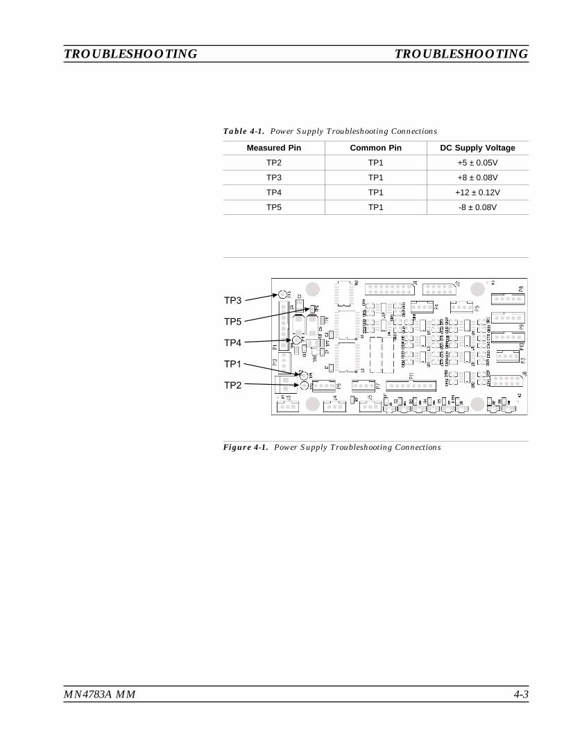
Step 7. Using a digital multimeter or an oscilloscope, measure the DC powersupply voltages listed in Table 4-1 (following page) by connecting thedigital multimeter or oscilloscope to the test points on the ControllerPCB assembly (shown in Figure 4-1 on the following page).
Step 8. If any of the DC voltage tests fail, replace the DC power supply as de-scribed in the removal and replacement procedures on page 5-8.
TROUBLESHOOTING TROUBLESHOOTING
4-2 MN4783A MM
TROUBLESHOOTING TROUBLESHOOTING
MN4783A MM 4-3
Measured Pin Common Pin DC Supply Voltage
TP2 TP1 +5 ± 0.05V
TP3 TP1 +8 ± 0.08V
TP4 TP1 +12 ± 0.12V
TP5 TP1 -8 ± 0.08V
Table 4-1. Power Supply Troubleshooting Connections
TP3
TP5
TP4
TP1
TP2
Figure 4-1. Power Supply Troubleshooting Connections

Directivity and TestPort Match Failure
If the system fails any of the directivity and test port match tests, per-form the following initial checks:
Step 1. Use a different calibration kit for measurement calibration and repeatthe Directivity Test. This step determines whether the calibration kitis the cause of the failure.
Step 2. Verify the performance of the MS462XC per Chapter 3 of theMS462XX Maintenance Manual (part number 10410-00205). This stepdetermines whether the MS462XC is the cause of the failure.
Step 3. If both the calibration kit and the MS462XC are okay, then go to thenext appropriate section of this troubleshooting procedure.
If the system fails the Directivity and Test Port Match tests at Port 1,perform the following checks:
Step 1. Perform the Port Module A check (refer to Section 4-5).
Step 2. If the insertion loss is too high, replace Port Module A (refer to the re-moval and replacement procedures for Bridge 1 on page 5-12).
Step 3. Verify that the directivity and test port match are now within specifi-cations.
Step 4. Perform the Port Module B check (refer to Section 4-5).
Step 5. If the insertion loss is too high, replace Port Module B (refer to the re-moval and replacement procedures for Bridge 3 on page 5-12).
Step 6. Verify that the directivity and test port match are now within specifi-cations.
Step 7. If the tests continue to fail, replace Switch 2 (refer to the removal andreplacement procedures for Switch 2 on page 5-10).
Step 8. Verify that the directivity and test port match are now within specifi-cations.
Step 9. If the tests continue to fail, perform the Combiner check (refer toSection 4-4).
If the System fails the Directivity and Test Port Match tests at Port 2,perform the following checks:
Step 1. Perform the Port Module C check (refer to Section 4-5).
Step 2. If the insertion loss is too high, replace Port Module C (refer to the re-moval and replacement procedures for Bridge 4 on page 5-12).
Step 3. Verify that the directivity and test port match are now within specifi-cations.
4-4 MN4783A MM
TROUBLESHOOTING TROUBLESHOOTING

Step 4. Perform the Port Module D check (refer to Section 4-5).
Step 5. If the test fails, replace Port Module D (refer to the removal and re-placement procedures for Bridge 2 on page 5-12).
Step 6. Verify that the directivity and test port match are now within specifi-cations.
Step 7. Perform the Test Channel Step Attenuator check (refer to Section 4-6).
Step 8. If the test fails, replace the Test Channel Step Attenuator (refer to theremoval and replacement procedures for the Step Attenuator onpage 5-6).
Step 9. Verify that the directivity and test port match are now within specifi-cations.
Step 10. If the test fails, replace the Power Divider (refer to the removal and re-placement procedures for Power Divider 1 on page 5-7).
Dynamic RangeFailure
If the system fails the Dynamic Range test, perform the following pro-cedure:
Step 1. Verify the performance of the MS462XC per Chapter 3 of theMS462XX Maintenance Manual (part number 10410-00205). This stepdetermines whether the MS462XC is the cause of the failure.
Step 2. Perform the Port Module D Check (refer to Section 4-5).
Step 3. If the test fails, replace Port Module D (refer to the removal and re-placement procedures for Bridge 2 on page 5-12).
Step 4. Verify that the system dynamic range is now within specifications.
Step 5. Perform the Test Channel Step Attenuator check (refer to Section 4-6).
Step 6. If the test fails, replace the Test Channel Step Attenuator (refer to theremoval and replacement procedures for the Step Attenuator onpage 5-6).
Step 7. Verify that the system dynamic range is now within specifications.
Step 8. If the test fails, replace the Power Divider (refer to the removal and re-placement procedures for Power Divider 2 on page 5-7).
4-3 OPERATIONAL CHECK Operational tests for the MN4783A consists of the following:
� Combiner Check
� Port Module Check
� Test Channel Step Attenuator Check
TROUBLESHOOTING OPERATIONAL CHECK
MN4783A MM 4-5

4-4 COMBINER CHECK This test checks whether the Combiner functions properly.
Equipment Required: The following equipment is required to perform the Combiner check:
� Anritsu ML243XA Power Meter
� Anritsu MA2472A Power Sensor
� Anritsu 2100-2 GPIB Interface Cable
� Anritsu 34NFNF50 Adapter
� Anritsu 3670NN50-2 Through Cable orAnritsu 15NN50-0.6B Cable
Setup: Set up the equipment as shown in Figure 4-2.
COMBINER CHECK TROUBLESHOOTING
4-6 MN4783A MM
MS4783ATest Set
ML243XAPower Meter
Connect as directed by the procedure
GPIB
Rear panel power meter GPIB connection
MS462X3CDRA Scorpion
Port 1 Port 2Port 3
POWER SENSOR
Cal / Zero
ML2408A Power Meter
����� �����
ON / OFF
Sensor Channel Trigger System
CALIBRATOR
0
1
4
7
2
5
8
+ / -
3
6
9
CLR
A
B
NoiseIn
Noise+28V
NO OPERATOR SERVICE-ABLE PARTS INSIDE.REFER SERVICING TOQUALIFIED PERSONNEL.
WARNING
CAUTIONFOR CONTINUED FIREPROTECTION REPLACEONLY WITH SPECIFIEDTYPE AND RATED FUSE.
IEEE 488.2GPIB
DedicatedGPIB
Serial Port Ethernet VGA SCSI-2
ExtAnalogOutput
ExtTrigger
LPT Line Printer Ext I/O
Port 1Port 2BiasBias
Port 2Bias Fuse
Port 1Bias Fuse
Ext AnalogIn
ExtSource
Ext 10 MHzIn
47-440 Hz85-264VAC
REPLACE FUSE ONLY WITHSAME TYPE AND RATING
CAUTIONDO NOT OPERATE
WITH POWER CORDUNGROUNDED
N274
00000001Made in UK
12-24V DC
(1.3A)
OUTPUT 1 OUTPUT 2 INPUT 1
DIGITAL
INPUT 2
ANALOG
CALIBRATORB
RS 232
PARALLEL PRINTER
GPIB / IEEE 488
CAUTION
DO NOT OPERATEWITH UNGROUNDEDPOWER CORD.
85-250 VAC
47-440Hz40VA MAX
SEE MANUAL FOR VOLTAGE RANGES ON BNC CONNECTORS
A
NO OPERATOR SERVICE-ABLE PARTS INSIDE.
WARNING
Figure 4-2. Test Equipment Setup for Combiner Check
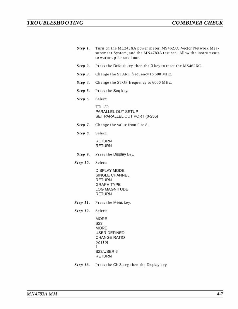
Step 1. Turn on the ML243XA power meter, MS462XC Vector Network Mea-surement System, and the MN4783A test set. Allow the instrumentsto warm-up for one hour.
Step 2. Press the Default key, then the 0 key to reset the MS462XC.
Step 3. Change the START frequency to 500 MHz.
Step 4. Change the STOP frequency to 6000 MHz.
Step 5. Press the Seq key.
Step 6. Select:
TTL I/OPARALLEL OUT SETUPSET PARALLEL OUT PORT (0-255)
Step 7. Change the value from 0 to 8.
Step 8. Select:
RETURNRETURN
Step 9. Press the Display key.
Step 10. Select:
DISPLAY MODESINGLE CHANNELRETURNGRAPH TYPELOG MAGNITUDERETURN
Step 11. Press the Meas key.
Step 12. Select:
MORES23MOREUSER DEFINEDCHANGE RATIOb2 (Tb)1S23/USER 6RETURN
Step 13. Press the Ch 3 key, then the Display key.
TROUBLESHOOTING COMBINER CHECK
MN4783A MM 4-7

Step 14. Select:
GRAPH TYPELOG MAGNITUDERETURN
Step 15. Press the Meas key.
Step 16. Select:
MORES21MOREUSER DEFINEDCHANGE RATIOb2 (Tb)1S21/USER 1RETURN
Step 17. Press the Config key.
Step 18. Select:
DATA POINTS201 MAX PTS
Step 19. Disconnect the N male connector of the interconnect RF cable from the“To Port 1” front panel connector. Refer to Figure 4-2.
Step 20. Zero and calibrate the power sensor. Install the 34NFNF50 adapter tothe input of the Power Sensor.
Step 21. Connect the Power Sensor to the end of the RF cable.
Step 22. Press Power key.
Step 23. Select:
SOURCE 1 SETUPFLAT TEST PORT POWER CALPOWER TARGET 0.00 dBmBEGIN CAL
Step 24. After the calibration is complete, remove the power sensor from the RFcable and reconnect the cable to “To Port 1” front panel connector.
Step 25. Disconnect the N male connector of the interconnect RF cable from the“To Port 3” front panel connector. Refer to Figure 4-2.
Step 26. Connect the power sensor to the end of the RF cable.
Step 27. Press the Power key.
COMBINER CHECK TROUBLESHOOTING
4-8 MN4783A MM

Step 28. Select:
SOURCE 2 SETUPFLAT TEST PORT POWER CALPOWER TARGET 0.00 dBmBEGIN CAL
Step 29. After the calibration is complete, remove the power sensor from the RFcable and reconnect the cable to the “To Port 3” front panel connector.
Test Procedure:
Step 1. Connect a through cable between Test Port 1 and Test Port 2 of theMN4783A test set.
Step 2. Press the Display key.
Step 3. Select:
TRACE MEMORY
Step 4. Allow the trace to sweep twice.
Step 5. Select:
STORE DATA TO MEMORYDISK OPERATIONSSAVE MEMORY TO HARD DISKCREATE NEW FILE
Step 6. Enter “COMBTST” as the file name and select DONE to save the datato the hard disk.
Step 7. Press the CH1 key.
Step 8. Press the Display key.
Step 9. Select:
TRACE MEMORYDISK OPERATIONSRECALL MEMORY FROM HARD DISKCOMBTST NRMVIEW DATA (/) MEMORY
Step 10. Verify that the slope of the displayed trace is less than 1 dB.
Step 11. If the slope is larger than 1 dB, compare the two traces and determinewhether the Port 1 or Port 3 path is the cause of the problem. Replacethe appropriate amplifier or combiner as needed.
TROUBLESHOOTING COMBINER CHECK
MN4783A MM 4-9

4-5 PORT MODULE CHECK This test checks whether the Port 1 and Port 2 modules function prop-erly.
Equipment Required: The following equipment is required to perform the port module check:
� Gore PhaseFlex™ cables (p/n EJD01D01048.0) (2 each)or equivalent
� Anritsu 34SFSF50 adapter or equivalent
� Anritsu 34NKF50 adapters (2 each) or equivalent
� Anritsu 28N50LF termination or equivalent
� Anritsu 28L50LF termination or equivalent
Setup: Set up the test equipment as described below:
Step 1. Disconnect all inter-connect RF cables between the MS462XC VectorNetwork Measurement System and the MN4783A test set.
NOTEDo not disconnect the cable connected between Ext I/O portof the MS462XC and Control In port of the MN4783A.
Step 2. Connect the MS462XC as shown in Figure 4-3.
Step 3. Connect a through cable between the C1 and C2 connector ports of theMN4783A.
Step 4. Turn on the MS462XC Vector Network Measurement System and theMN4783A test set. Allow the system to warm-up for one hour.
Step 5. Press the Default key, then the 0 key to reset the MS462XC.
4-10 MN4783A MM
PORT MODULE CHECK TROUBLESHOOTING
Data Entry
PowerKeyboard
Port 3
Channels Enhancement
Stimulus System
Port 1 Port 2
Probe Power
MS4623B Vector Network Measurement System10 MHz-6 GHz
1
8
5
2
9
6
3
-.
G/ns/m
M/ s/cmµ
k/ms/mm
X1
Enter
Local
Appl
Meas
Marker
Hold
Ch 1 Ch 2
Ch 4Ch 3
Freq Sweep
Power Config
Seq Cal
Avg Utility
Hard
Copy
DefaultSave /
Recall
0
7
4
Display
Clr
NoiseIn
Noise+28V
NO OPERATOR SERVICE-ABLE PARTS INSIDE.REFER SERVICING TOQUALIFIED PERSONNEL.
WARNING
CAUTIONFOR CONTINUED FIREPROTECTION REPLACEONLY WITH SPECIFIEDTYPE AND RATED FUSE.
IEEE 488.2GPIB
DedicatedGPIB
Serial Port Ethernet VGA SCSI-2
ExtAnalogOutput
ExtTrigger
LPT Line Printer Ext I/O
Port 1Port 2BiasBias
Port 2Bias Fuse
Port 1Bias Fuse
Ext AnalogIn
ExtSource
Ext 10 MHzIn
47-440 Hz85-264VAC
REPLACE FUSE ONLY WITHSAME TYPE AND RATING
CAUTIONDO NOT OPERATE
WITH POWER CORDUNGROUNDED
N274
MS462XC Front Panel
Port 1b2 input
34SFSF50 Adapter
Cable A4 foot Gore PhaseFlexcable (part number EJD01D01048.0)
Cable B4 foot Gore PhaseFlexcable (part number EJD01D01048.0)
MS462XC Rear Panel
Figure 4-3. Coupler Check Test Setup

Step 6. Change the START frequency to 10 MHz.
Step 7. Change the STOP frequency to 6000 MHz.
Step 8. Press the Ch3 key, then the Display key.
Step 9. Select:
DISPLAY MODESINGLE CHANNELRETURNGRAPH TYPELOG MAGNITUDERETURN
Step 10. Press the Meas key.
Step 11. Select:
MORES21MOREUSER DEFINEDCHANGE RATIOb2 (Tb)1S21/USER 1RETURN
Step 12. Press Power key.
Step 13. Select:
SOURCE 1 SETUPPORT 1 ATTN 2*10 dB (0 – 70)
Step 14. Verify that the PORT 1 POWER is below –15 dBm. Adjust theSOURCE 1 POWER control if necessary.
Step 15. Connect the two cables together with the 34SFSF50 adapter.
Step 16. Press the Display key.
Step 17. Select:
TRACE MEMORY
Step 18. Allow the trace to sweep twice, then select:
STORE DATA TO MEMORYVIEW DATA (/) MEMORY
Step 19. Disconnect the connection between cable A and cable B at the adapter.
TROUBLESHOOTING PORT MODULE CHECK
MN4783A MM 4-11

Test Procedure:
Step 1. Disconnect the Ext Pre-Amp RF loop cable between the Input andOutput connectors.
Step 2. Connect cable A, cable B, and the terminations to the connector portsas indicated in Table 4-3. Refer to Figure 4-3 and Figure 4-4 (followingpage) for the connector locations.
Step 3. Verify that the insertion loss in the corresponding path is within thetolerance as stated in Table 4-3.
Step 4. Repeat the test for the rest of the signal paths stated in Table 4-3.
Step 5. Reconnect all of the inter-connect RF cables between the MS462XCVector Network Measurement System and MN4783A test set. Also,reconnect the Ext Pre Amp RF loop cable.
PORT MODULE CHECK TROUBLESHOOTING
4-12 MN4783A MM
TestsCable A
(from Port 1 of MS462XC)Cable B
(to b1 Input of MS462XC)Termination
InsertionLoss
A External Pre-Amp Output connectorof the MN4783A
a1 Output connector of theMN4783A
Test Port 1 connector � 21 dB
B Test Port 1 connector of theMN4783A
b1 Output connector of theMN4783A
Ext Pre-Amp Output con-nector of the MN4783A
� 21 dB
C Test Port 2 connector of theMN4783A
Aux Out connector of theMN4783A
b2 Output connector andTo Port 2 connector of theMN4783A
�24 dB
D To Port 2 connector of theMN4783A
a2 Output connector of theMN4783A
C1 connector of theMN4783A
� 21 dB
Table 4-3. Troubleshooting Connections

TROUBLESHOOTING PORT MODULE CHECK
MN4783A MM 4-13
Noise Out
Noise
Source
C1 C2
a1 a2 b1 b2 ControlIn
Figure 4-4. Test Set Rear Panel
Figure 4-3. Test Set Front Panel

4-6 TEST CHANNEL STEPATTENUATOR CHECK
This test checks whether the Test Channel Step Attenuator functionsproperly.
Setup: Set up the test equipment as described below:
Step 1. Turn on the MS462XC Vector Network Measurement System and theMN4783A test set and allow the equipment to warm-up for one hour.
Step 2. Press the Default key and then 0 key.
Step 3. Press the Seq key.
Step 4. Select:
TTL I/OPARALLEL OUT SETUPSET PARALLEL OUT PORT (0-255)
Step 5. Change the value from 0 to 8.
Step 6. Select:
RETURNRETURN
Step 7. Press the Display key.
Step 8. Select:
DISPLAY MODESINGLE CHANNELRETURN
Step 9. Press the Ch 3 key, then the Display key.
Step 10. Select:
GRAPH TYPELOG MAGNITUDERETURN
Step 11. Press the Avg key.
Step 12. Select:
SELECT I.F. BANDWIDTHI. F. BW 10 Hz
TEST CHANNEL STEP ATTENUATOR CHECK TROUBLESHOOTING
4-14 MN4783A MM

Test Procedure:
Step 1. Connect a through cable between Test Port 1 and Test Port 2.
Step 2. Select:
TRACE MEMORY
Step 3. Allow the trace to sweep twice.
Step 4. Select:
STORE DATA TO MEMORYVIEW DATA (/) MEMORYRETURN
Step 5. Select:
SCALE10 dB/DIV
Step 6. Press the Seq key.
Step 7. Select:
TTL I/OPARALLEL OUT SETUPSET PARALLEL OUT PORT (0-255)
Step 8. Change the SET PARALLEL OUT PORT value to 9.
Step 9. Verify that the displayed S21 trace is within the range specified in Ta-ble 4-6.
Step 10. Repeat Step 7 and Step 8 for the other PARALLEL OUT PORT valueslisted in Table 4-6.
TROUBLESHOOTING TEST CHANNEL STEP ATTENUATOR CHECK
MN4783A MM 4-15/4-16
Parallel Out Port ValueCorresponding StepAttenuator Setting
Expected Range
9 10 dB 10 ± 1 dB10 20 dB 20 ± 1 dB12 40 dB 40 ± 2 dB
Table 4-6. Step Attenuator Specifications


Chapter 5Removal and ReplacementProcedures
5-1 INTRODUCTION This chapter provides procedures for removing and reinstalling thereplaceable subassemblies listed in Chapter 2, Table 2-1.
5-2 EQUIPMENT REQUIRED All procedures in this chapter require the use of either a #1 or #2 sizePhillips type screw driver. Most procedures require the use of a5/16 inch wrench and the Anritsu 01-201 (8 inch-pounds) torquewrench. Some procedures require the use of a small jewelers Phillipsscrewdriver.
CAUTIONAlways use a torque wrench calibrated to 8 inch-poundswhen tightening SMA connectors. Over-torquing will causedamage to the RF connectors.
5-3 REMOVING THE COVERS Troubleshooting operations require removal of the top cover.Replacement of some test set assemblies and parts require removal ofall covers. The following procedure describes this process.
Preliminary:
Step 1. Switch the test set power off and remove the power cord.
Step 2. Remove the test set from the ME7840/4 test system by disconnectingall cable connections and separating the test set from the MS462XC.
Procedure: Refer to Figure 5-1, page 5-3, during this procedure.
NOTEIt is only necessary to loosen the test set’s front handleassemblies to remove the top, bottom, or side covers.However, if the front panel is to be removed, the handleassemblies should also be removed.
MN4783A MM 5-1

Step 1. Loosen (or remove) the right and left handle assemblies as follows:
a. Place the test set on its top (bottom-side up).
b. Loosen (or remove) the screws at the sides of the handle assem-blies.
c. If removing the handles, pull them away from the unit and setthem aside.
CAUTIONThe green headed screws have metric threads. Be sure toretain all of the screws and replace them in their originallocation.
Step 2. To remove the top cover:
a. Place the test set in the normal (top-side up) position.
b. Remove the feet from the two top corners at the rear of the testset.
c. Remove the center screw from the rear of the top cover.
d. Lift and slide the top cover away from the test set.
Step 3. To remove the bottom cover:
a. Place the test set on its top (bottom-side up).
b. Remove the feet from the two bottom corners at the rear of the testset.
c. Remove the center screw from the rear of the bottom cover.
d. Lift and slide the bottom cover away from the test set.
Step 4. To remove the right cover:
a. Place the test set on its left side.
b. Remove the feet from the two right-side corners at the rear of thetest set.
c. Remove the center screw from the right cover.
d. Lift and slide the side cover away from the test set.
Step 5. To remove the left cover:
a. Place the test set its right side.
b. Remove the feet from the two left-side corners at the rear of thetest set.
c. Remove the center screw from the rear of the left side cover.
d. Lift and slide the side cover away from the test set.
REMOVING THE COVERS REMOVAL AND REPLACEMENT
5-2 MN4783A MM

To replace the instrument covers, perform the previous steps in thereverse order.
REMOVAL AND REPLACEMENT REMOVING THE COVERS
MN4783A MM 5-3
Figure 5-1. MN4783A Test Set Cover Removal

5-4 CONTROL PCB This Section provides a procedure for removing and replacing the Con-trol PCB in the test set.
Step 1. Remove the top cover from the test set (Section 5-3).
Step 2. Disconnect the wires from connectors P1, P6, P8, P9, P10, J1, J2, J3,J4, and J5on the Control PCB (Figure 5-2).
Step 3. Use a #1 Phillips screwdriver to remove the four mounting screws.
Step 4. Lift the Control PCB assembly out from the test set chassis.
To replace the Control PCB, reverse the order of the removalprocedure.
CONTROL PCB REMOVAL AND REPLACEMENT
5-4 MN4783A MM
Remove
Mounting Screws (4)
Disconnect
Wire Connections (10)
Switch 1
Switch 2
Switch 3
Power Supply
Power Divider 2
Power Divider 1
Bridge 1
Bridge 3
Bridge 2
Bridge 4
AMP 1
AMP 2
Fan
JS
P
JS
P
JSP
JS
P
AT
TE
NU
AT
OR
JB
JB
JB
JB
Control PCB
Figure 5-2. Control PCB Removal

5-5 RF AMPLIFIERS This Section provides a procedure for removing and replacing the twoRF Amplifiers in the test set.
Step 1. Remove the top cover from the test set (Section 5-3).
Step 2. Disconnect the two RF cables from the RF amplifier with a 5/16-inchwrench (Figure 5-3).
Step 3. Disconnect the appropriate supply wire from J3 or P6 on the ControlPCB.
Step 4. Remove the two amplifier mounting screws from the mounting bracketwith a #1 Phillips screwdriver.
Step 5. Lift the amplifier out from the test set chassis.
Step 6. Remove the two Phillips screws that secure the amplifier to themounting bracket.
To replace the amplifiers, reverse the order of the removal procedure.
REMOVAL AND REPLACEMENT RF AMPLIFIERS
MN4783A MM 5-5
Switch 1
Switch 2
Switch 3
Power Supply
Power Divider 2
Power Divider 1
Bridge 1
Bridge 3
Bridge 2
Bridge 4
AMP 1
AMP 2
Fan
JS
P
JS
P
JSP
JS
P
AT
TE
NU
AT
OR
JB
JB
JB
JB
Control PCB
Remove
RF Cables
Remove Mounting
Screws (2)
Disconnect
Supply Wires
Amplifier Detail
Remove
Mounting Screws (2)
Figure 5-3. Amplifier 1 and Amplifier 2 Removal

5-6 STEP ATTENUATOR This Section provides a procedure for removing and replacing theStep Attenuator in the test set.
Step 1. Remove the top cover from the test set (Section 5-3).
Step 2. Disconnect the Step Attenuator ribbon-cable from the Attenuator (Fig-ure 5-4).
Step 3. Disconnect the RF cables from the Step Attenuator using a 5/16-inchwrench.
Step 4. Remove the two Step Attenuator mounting screws from the mountingbracket with a #1 Phillips screwdriver.
Step 5. Lift the Step Attenuator out from the test set chassis.
Step 6. Remove the two larger Phillips screws that secure the attenuator tothe mounting bracket.
To replace the Step Attenuator, reverse the order of the removalprocedure.
STEP ATTENUATOR REMOVAL AND REPLACEMENT
5-6 MN4783A MM
Switch 1
Switch 2
Switch 3Power Supply
Power Divider 2
Power Divider 1
Bridge 1
Bridge 3
Bridge 2
Bridge 4
AMP 1
AMP 2
Fan
JS
P
JS
P
JSP
JS
P
Atten
uato
r
JB
JB
JB
JB
Control PCB
Remove Mounting
Screws (2)
Remove
RF Cables
Disconnect
Ribbon Cable
Remove RF Cables
Remove Ribbon Cable
Remove Larger Mounting Screws
Figure 5-4. Step Attenuator Removal

5-7 POWER DIVIDERS This Section provides a procedure for removing and replacing thePower Dividers in the test set.
Step 1. Remove the top cover from the test set (Section 5-3).
Step 2. Disconnect the three RF cables from the Power Divider using a5/16-inch wrench (Figure 5-5).
Step 3. Remove the two Power Divider mounting screws with a #1 Phillipsscrewdriver.
Step 4. Lift the Power Divider out from the chassis.
To replace the Power Divider, reverse the order of the removal proce-dure.
REMOVAL AND REPLACEMENT POWER DIVIDERS
MN4783A MM 5-7
Switch 1
Switch 2
Switch 3
Power Supply
Power Divider 2
Power Divider 1
Bridge 1
Bridge 3
Bridge 2
Bridge 4
AMP 1
AMP 2
Fan
JS
P
JS
P
JSP
JS
P
AT
TE
NU
AT
OR
JB
JB
JB
JB
Control PCB
Disconnect
RF Cables (3)
Remove Mounting
Screws (2)
Figure 5-5. Power Divider Removal

5-8 POWER SUPPLY This Section provides a procedure for removing and replacing thePower Supply in the test set.
Step 1. Remove the top and bottom covers from the test set (Section 5-3).
Step 2. Disconnect all of the wire connections from the Power Supply (Fig-ure 5-6).
Step 3. Turn the test set on its side.
POWER SUPPLY REMOVAL AND REPLACEMENT
5-8 MN4783A MM
Red Black
Blue
Brown
Green/Yellow
LED
Switch 1
Switch 2
Switch 3
Power Supply
Power Divider 2
Power Divider 1
Bridge 1
Bridge 3
Bridge 2
Bridge 4
AMP 1
AMP 2
Fan
JS
P
JS
P
JSP
JS
P
AT
TE
NU
AT
OR
JB
JB
JB
JB
Control PCB
Disconnect Power Supply
I/O Connections
Figure 5-6. Power Supply Removal (Top View)

Step 4. Hold the Power Supply and remove the four mounting screws with a#1 Phillips screwdriver (Figure 5-7).
Step 5. Lift the Power supply out from the test set chassis.
To replace the Power Supply, reverse the order of the removal proce-dure.
REMOVAL AND REPLACEMENT POWER SUPPLY
MN4783A MM 5-9
Remove Power Supply
Mounting Screws (4)
Figure 5-7. Power Supply Removal (Bottom View)

5-9 RF SWITCHES This Section provides a procedure for removing and replacing thethree RF Switches.
Step 1. Remove the top cover from the test set (Section 5-3).
Step 2. Use a 5/16 inch wrench to disconnect the three RF cables from the RFSwitch to be removed (Figure 5-8).
Step 3. Disconnect the appropriate wire connector from the Control PCB.
Step 4. Remove the two mounting screws from the mounting bracket with a#1 Phillips screwdriver.
RF SWITCHES REMOVAL AND REPLACEMENT
5-10 MN4783A MM
Switch 1
Switch 2
Switch 3
Power Supply
Power Divider 2
Power Divider 1
Bridge 1
Bridge 3
Bridge 2
Bridge 4
AMP 1
AMP 2
Fan
JS
P
JS
P
JSP
JS
P
AT
TE
NU
AT
OR
JB
JB
JB
JB
Control PCB
Disconnect
RF Cables (3)
Remove
Mounting Screws (2)
Disconnect
Wire Connection
Figure 5-8. RF Switch Removal

Step 5. Lift the RF Switch out from the test set chassis.
Step 6. Remove the two Phillips screws that secure the RF Switch to themounting bracket (Figure 5-9).
To replace the RF Switch, reverse the order of the removal procedure.
REMOVAL AND REPLACEMENT RF SWITCHES
MN4783A MM 5-11
Switch 2
Switch 1
Switch 3
Remove
Mounting Screws (2)
Figure 5-9. Switch Wiring and Bracket Detail

5-10 PORT MODULES This section provides a procedure for removing and replacing the portmodules (VSWR Bridges) in the test set.
Step 1. Remove the top cover from the test set (Section 5-3).
Step 2. Use a 5/16 inch wrench to disconnect the RF cable connections on theport module at ports P, JB, and JS (Figure 5-10).
Step 3. Use a #1 Phillips screwdriver to remove the three mounting screws.
Step 4. Lift the port module out from the test set chassis.
To replace the port module, reverse the order of the removal proce-dure.
PORT MODULES REMOVAL AND REPLACEMENT
5-12 MN4783A MM
Switch 1
Switch 2
Switch 3
Power Supply
Power Divider 2
Power Divider 1
Bridge 1
Bridge 3
Bridge 2
Bridge 4
AMP 1
AMP 2
Fan
JS
P
JS
P
JSP
JS
P
AT
TE
NU
AT
OR
JB
JB
JB
JB
Control PCB
Disconnect
RF Cables (3)
Remove
Mounting Screws (3)
Figure 5-10. Port Module Removal

5-11 FAN ASSEMBLY This Section provides a procedure for removing and replacing the rearpanel fan assembly.
Step 1. Remove the top cover from the test set (Section 5-3).
Step 2. Disconnect the fan supply wire at J3 of the control PCB (Refer to Sec-tion 5-4 for a diagram).
Step 3. Use a #1 Phillips screwdriver to remove the four screws holding thefan guard in place (Figure 5-11).
Step 4. Remove the fan guard and lift the fan out from the chassis.
To replace the fan, reverse the order of the removal procedure.
REMOVAL AND REPLACEMENT FAN ASSEMBLY
MN4783A MM 5-13/5-14
Figure 5-11. Fan Removal


Appendix AConnector MaintenanceCheck Procedures
A-1 INTRODUCTION This appendix provides general, precautionary information and in-structions pertaining to precision connectors.
A-2 PRECAUTIONS The following paragraphs are precautionary notes relating to mainte-nance considerations for precision connectors
Pin Depth Problems Based on Anritsu precision components returned for repair, destruc-tive pin depth of mating connectors is the major cause of failure in thefield. When a precision component is mated with a connector having adestructive pin depth, damage will likely occur to the precision compo-nent’s connector. A connector is considered to have destructive pindepth when the center pin is too long in respect to the connector’s ref-erence plane (Figure A-1).
Before mating an unknown or new device with your test set Port con-nectors or calibration devices, always measure the pin depth of the de-vice’s connectors. Use an Anritsu Pin Depth Gauge, or equivalent, forthese measurements (Figure A-2, following page). Also, measure theconnector pin-depth of a device when intermittent or degraded perfor-mance is suspected.
Gauging sets for measuring the pin-depth of precision connectors areavailable from your nearest Anritsu Service center, or from the factory.Instructions for measuring connector pin-depth are included with thegauging set(s).
MN4783A MM A-1
REFERENCEPLANE
MALE
PINDEPTH
(INCHES)
REFERENCEPLANE
FEMALE
PINDEPTH
(INCHES)
Figure A-1. N Connector Pin DepthDefinition

Pin-Depth Tolerance The center pin of a precision connector has a tolerances measured inmils (one mil = 1/1000 inch). The connectors of test devices may not beprecision types and they may not have the proper pin-depth. Theseconnectors should be measured before mating to ensure suitability.
When gauging pin depth, if the connector being measured indicatesout of tolerance in the “+” region of the gauge (Table A-1), the centerpin is too long. Mating under this condition will likely damage the mat-ing connector. On the other hand, if the test device connector indicatesout of tolerance in the “–” region, the center pin is too short. While thiswill not cause any damage, it will result in a poor connection and aconsequent degradation in performance.
A-2 MN4783A MM
PRECAUTIONS APPENDIX A
PortConnector Type
Pin Depth(MILS)
GaugeReading
GPC-7 +0.000–0.003
Same AsPin Depth
N Male 207 –0.000+0.004
207 +0.000–0.004
N Female 207 –0.004+0.000
Same AsPin Depth
3.5 mm Male, Female –0.000+0.002
K Male, Female +0.0000–0.0035
V Male +0.000–0.001
V Female +0.000–0.001
Table A-1. Connector Pin-Depth Tolerance
01
2
3
45
1
2
3
4
21 1
2
Figure A-2. Pin Depth Gauge

Avoid Over TorquingConnectors
Over-torquing connectors is destructive; it may damage the connectorcenter pin. Finger-tight is usually sufficient, especially on Type N con-nectors. Should it be necessary to use a wrench to tighten SMA orWSMA connectors, use a torque wrench that breaks at 8 inch-pounds.As a general rule, never use pliers to tighten connectors.
Teflon TuningWashers
The center conductor on many precision connectors contains a smallTeflon tuning washer located near the point of mating (interface). Thiswasher compensates for minor impedance discontinuities at the inter-face. The washer’s location is critical to the connector’s performance.Do not disturb it.
Avoid MechanicalShock
Precision connectors are designed to withstand years of normal benchhandling. Do not drop or otherwise treat them roughly. They are labo-ratory-quality devices, and like other such devices, they require carefulhandling.
Keep ConnectorsClean
The precise geometry that makes a precision connector’s high perfor-mance possible can be disturbed by dirt and other contamination ad-hering to connector interfaces. When not in use, keep the connectorscovered.
Visual Inspection Precision connectors should be inspected periodically. Check for thefollowing:
� Bent or broken center pin� Damaged threads� Other bent or damaged connector parts� Dirt or foreign material in connector cavity.
A-3 REPAIR/MAINTENANCE Anritsu recommends that no maintenance other than cleaning be at-tempted by the customer. Any device with a suspected defective con-nector should be returned to Anritsu for repair and/or service whenneeded.
MN4783A MM A-3/A-4
APPENDIX A REPAIR/MAINTENANCE


Index
AAnritsu Service Centers · · · · · · · · · · · · 1-10Assembly Exchange Program· · · · · · · · · · 2-1Assembly Location Diagram (Top View)· · · · 2-3Avoid Mechanical Shock · · · · · · · · · · · · A-3
BBlock Diagram· · · · · · · · · · · · · · · · · · 1-3
CCabling Diagram (Top View) · · · · · · · · · · 2-5Combiner Check · · · · · · · · · · · · · 4-6 to 4-9Component Wiring Diagram · · · · · · · · · · 2-6Connector Maintenance
Cleaning · · · · · · · · · · · · · · · · · · · A-3Mechanical Shock · · · · · · · · · · · · · · A-3Pin Depth Problems · · · · · · · · · · · · · A-1Pin Depth Tolerances · · · · · · · · · · · · A-2Precautions· · · · · · · · · · · · · · · · · · A-1Repair/Maintenance · · · · · · · · · · · · · A-3Teflon Tuning Washer · · · · · · · · · · · · A-3Torque · · · · · · · · · · · · · · · · · · · · A-3Visual Inspection· · · · · · · · · · · · · · · A-3
Connectors and Ports, Description · · · · · · · 1-6Control PCB
Replacement · · · · · · · · · · · · · · · · · 5-4Conventions
in Manual · · · · · · · · · · · · · · · · · · · 1-2in Procedures · · · · · · · · · · · · · · · · · 3-1
Covers, Removing · · · · · · · · · · · · 5-1 to 5-3
DDescriptions
Connectors and Ports· · · · · · · · · · · · · 1-6DRA Scorpion· · · · · · · · · · · · · · · · · 1-4MN4783A · · · · · · · · · · · · · · · · · · · 1-5System · · · · · · · · · · · · · · · · · 1-4 to 1-7Test Set · · · · · · · · · · · · · · · · · · · · 1-5
Diagram, Block · · · · · · · · · · · · · · · · · 1-3Directivity and Test Port Match Failure · · · · 4-4Directivity and Test Port Match Test · · 3-4 to 3-6Drawing, Rear Panel · · · · · · · · · · · · · · 1-7Dynamic Range Failure · · · · · · · · · · · · · 4-5
EElectro-static Discharge Procedures · · · · · · 1-8Equipment, Required for
Removing and Replacing Subassemblies · · 5-1Exchange Assembly Program· · · · · · · · · · 2-1
FFan Assembly
Replacement· · · · · · · · · · · · · · · · · 5-13
HHardware Description · · · · · · · · · · 1-2 to 1-3
IIdentification Number · · · · · · · · · · · · · 1-2
MMaintenance, of Connectors · · · · · · · · · · A-3Major Assemblies
Cabling Diagram (Top View)· · · · · · · · · 2-5Location Diagram (Top View) · · · · · · · · 2-3Wiring Diagram (Top View) · · · · · · · · · 2-4
Manual Scope · · · · · · · · · · · · · · · · · · 1-1Manuals, Related · · · · · · · · · · · · · · · · 1-1ME7840/4
Block Diagram · · · · · · · · · · · · · · · · 1-3Hardware · · · · · · · · · · · · · · · · · · · 1-2
MN4783ABlock Diagram · · · · · · · · · · · · · · · · 1-3Rear Panel Drawing · · · · · · · · · · · · · 1-7Test Set Description · · · · · · · · · · · · · 1-5
MS462XC Rear Panel Drawing· · · · · · · · · 1-7
OOperational Check · · · · · · · · · · · · · · · 4-5
Combiner · · · · · · · · · · · · · · · 4-6 to 4-9Port Module · · · · · · · · · · · · · 4-10 to 4-13Step Attenuator· · · · · · · · · · · 4-14 to 4-15
Ordering Information, Parts · · · · · · · 2-2 to 2-6
MN4783A MM Index-1
INDEX A TO O

PParts Ordering Information · · · · · · · 2-2 to 2-6Pin Depth
Problems · · · · · · · · · · · · · · · · · · · A-1Tolerances · · · · · · · · · · · · · · · · · · A-2
Port ModuleCheck · · · · · · · · · · · · · · · · 4-10 to 4-13Replacement· · · · · · · · · · · · · · · · · 5-12
Ports and Connectors, Description · · · · · · · 1-6Power Divider
Replacement · · · · · · · · · · · · · · · · · 5-7Power Up Failure · · · · · · · · · · · · · · · · 4-2Precautions · · · · · · · · · · · · · · · · · · · A-1
RRear Panel
Drawing· · · · · · · · · · · · · · · · · · · · 1-7Recommended Test Equipment · · · · 1-8 to 1-10Related Manuals · · · · · · · · · · · · · · · · 1-1Removal and Replacement Procedures
Control PCB · · · · · · · · · · · · · · · · · 5-4Covers · · · · · · · · · · · · · · · · · 5-1 to 5-3Equipment Required · · · · · · · · · · · · · 5-1Fan Assembly · · · · · · · · · · · · · · · · 5-13Port Module · · · · · · · · · · · · · · · · · 5-12Power Divider · · · · · · · · · · · · · · · · 5-7RF Amplifiers· · · · · · · · · · · · · · · · · 5-5RF Switch · · · · · · · · · · · · · · 5-10 to 5-11Step Attenuator · · · · · · · · · · · · · · · 5-6
Repair, of Connectors · · · · · · · · · · · · · · A-3Replaceable Subassemblies · · · · · · · · · · · 2-2Replaceable Subassemblies and Parts · · · · · 2-2Required Equipment for
Removing and Replacing Subassemblies · · 5-1RF Amplifiers
Replacement · · · · · · · · · · · · · · · · · 5-5RF Switch
Replacement · · · · · · · · · · · · 5-10 to 5-11
SScope of Manual · · · · · · · · · · · · · · · · · 1-1Scorpion
DRA Description · · · · · · · · · · · · · · · 1-4Rear Panel Drawing · · · · · · · · · · · · · 1-7
Serial Interface PCBReplacement · · · · · · · · · · · · · · · · · 5-4
Service Centers · · · · · · · · · · · · · · · · 1-10Source Output Accuracy Test · · · · · · 3-2 to 3-3Static Precautions· · · · · · · · · · · · · · · · 1-8Step Attenuator
Replacement · · · · · · · · · · · · · · · · · 5-6Step Attenuator Check · · · · · · · · 4-14 to 4-15System Description· · · · · · · · · · · · 1-4 to 1-7System Dynamic Range Test · · · · · · 3-7 to 3-10System Overview · · · · · · · · · · · · · · · · 1-2
TTeflon Tuning Washers · · · · · · · · · · · · A-3Test Procedure Conventions · · · · · · · · · · 3-1Test Set
Description · · · · · · · · · · · · · · · · · · 1-5Rear Panel Drawing · · · · · · · · · · · · · 1-7
Torquing Connectors · · · · · · · · · · · · · · A-3Troubleshooting · · · · · · · · · · · · · 4-1 to 4-4
Combiner Check · · · · · · · · · · · · 4-6 to 4-9Directivity · · · · · · · · · · · · · · · · · · 4-4Dynamic Range· · · · · · · · · · · · · · · · 4-5Operational Check · · · · · · · · · · · · · · 4-5Port Module Check · · · · · · · · · 4-10 to 4-13Power-up Failure · · · · · · · · · · · · · · · 4-2Step Attenuator Check · · · · · · · 4-14 to 4-15Test Port Match · · · · · · · · · · · · · · · 4-4
VVerification Procedures
Directivity · · · · · · · · · · · · · · · 3-4 to 3-6Source Output Accuracy · · · · · · · 3-2 to 3-3System Dynamic Range · · · · · · · 3-7 to 3-10Test Port Match · · · · · · · · · · · · 3-4 to 3-6
Visual Inspection · · · · · · · · · · · · · · · · A-3
WWiring Diagram
of Components · · · · · · · · · · · · · · · · 2-6of Test Set· · · · · · · · · · · · · · · · · · · 2-4
Index-2 MN4783A MM
P TO W INDEX

