application note sky77336 power amplifier … power amplifier module ... pa output power is...
TRANSCRIPT
Skyworks Solutions, Inc. • Phone [781] 376-3000 • Fax [781] 376-3100 • [email protected] • www.skyworksinc.com 200938A • Skyworks Proprietary and Confidential Information. • Products and product information are subject to change without notice. • September 9, 2008 1
APPLICATION NOTE
SKY77336 Power Amplifier Module – Evaluation Information Applicability: SKY77336 Power Amplifier Modules
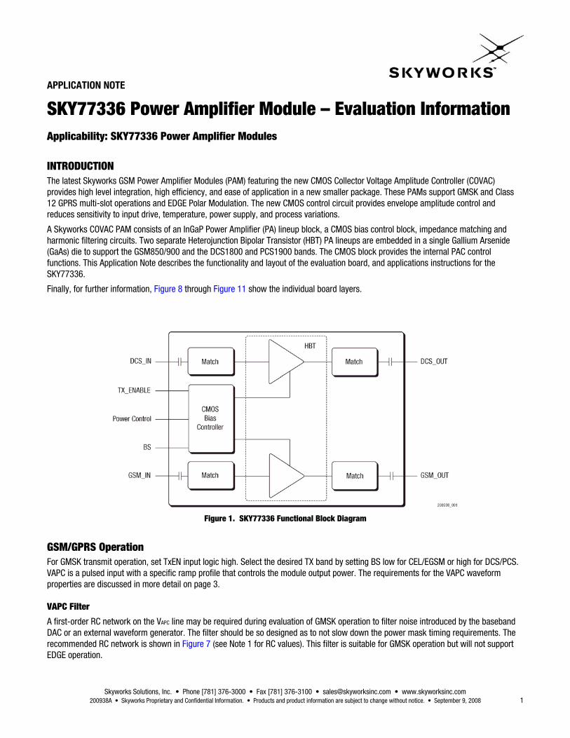
INTRODUCTION The latest Skyworks GSM Power Amplifier Modules (PAM) featuring the new CMOS Collector Voltage Amplitude Controller (COVAC) provides high level integration, high efficiency, and ease of application in a new smaller package. These PAMs support GMSK and Class 12 GPRS multi-slot operations and EDGE Polar Modulation. The new CMOS control circuit provides envelope amplitude control and reduces sensitivity to input drive, temperature, power supply, and process variations.
A Skyworks COVAC PAM consists of an InGaP Power Amplifier (PA) lineup block, a CMOS bias control block, impedance matching and harmonic filtering circuits. Two separate Heterojunction Bipolar Transistor (HBT) PA lineups are embedded in a single Gallium Arsenide (GaAs) die to support the GSM850/900 and the DCS1800 and PCS1900 bands. The CMOS block provides the internal PAC control functions. This Application Note describes the functionality and layout of the evaluation board, and applications instructions for the SKY77336.
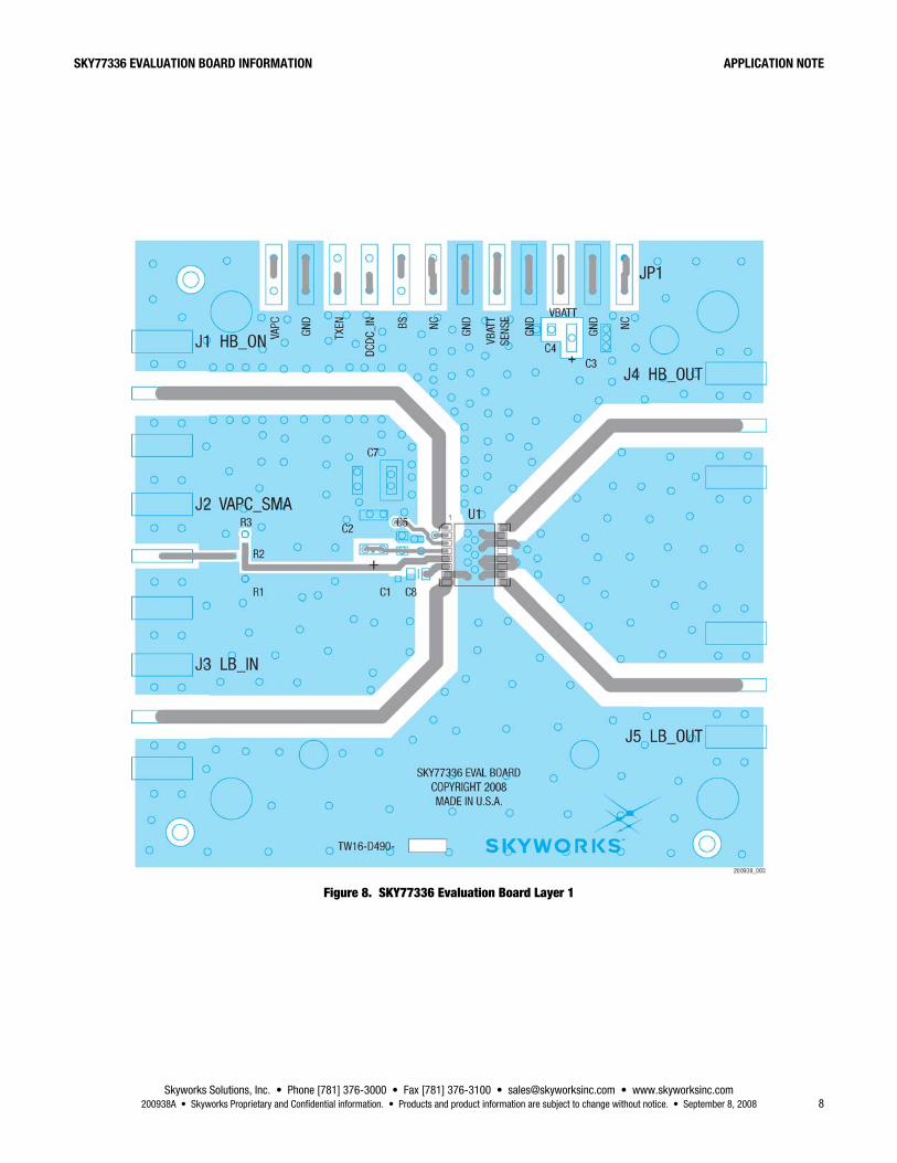
Finally, for further information, Figure 8 through Figure 11 show the individual board layers.
Figure 1. SKY77336 Functional Block Diagram
GSM/GPRS Operation For GMSK transmit operation, set TxEN input logic high. Select the desired TX band by setting BS low for CEL/EGSM or high for DCS/PCS. VAPC is a pulsed input with a specific ramp profile that controls the module output power. The requirements for the VAPC waveform properties are discussed in more detail on page 3.
VAPC Filter
A first-order RC network on the VAPC line may be required during evaluation of GMSK operation to filter noise introduced by the baseband DAC or an external waveform generator. The filter should be so designed as to not slow down the power mask timing requirements. The recommended RC network is shown in Figure 7 (see Note 1 for RC values). This filter is suitable for GMSK operation but will not support EDGE operation.
APPLICATION NOTE SKY77336 EVALUATION BOARD INFORMATION
Skyworks Solutions, Inc. • Phone [781] 376-3000 • Fax [781] 376-3100 • [email protected] • www.skyworksinc.com 2 September 9, 2008 • Skyworks Proprietary and Confidential Information. • Products and product information are subject to change without notice. • 200938A
Depending on the operating characteristics of the baseband DAC, the RC network must be carefully designed or eliminated. Increasing the resistor value might have a negative impact on voltage drop, and consequently, PA output power. The loop bandwidth requirement of the Polar Loop Transmitter architecture must be considered if such a filter is needed.
Power Control Scheme:
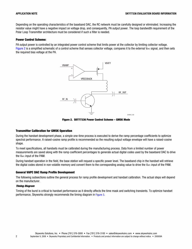
PA output power is controlled by an integrated power control scheme that limits power at the collector by limiting collector voltage. Figure 2 is a simplified schematic of a control scheme that senses collector voltage, compares it to the external VAPC signal, and then sets the required bias voltage at the PA.
Figure 2. SKY77336 Power Control Scheme – GMSK Mode
Transmitter Calibration for GMSK Operation
During the handset development phase, a simple one-time process is executed to derive the ramp percentage coefficients to optimize spectral performance. A raised-cosine ramp profile is recommended so the resulting output voltage envelope will have a raised-cosine shape.
To meet specifications, all handsets must be calibrated during the manufacturing process. Data from a limited number of power measurements are saved along with the ramp coefficient percentages to generate actual digital codes used by the baseband DAC to drive the VAPC input of the PAM.
During handset operation in the field, the base station will request a specific power level. The baseband chip in the handset will retrieve the digital codes stored in non-volatile memory and convert them to the corresponding analog value to drive the VAPC input of the PAM.
General VAPC DAC Ramp Profile Development
The following subsections outline the general process for ramp profile development and handset calibration. The actual steps will depend on the manufacturer.
Timing Diagram
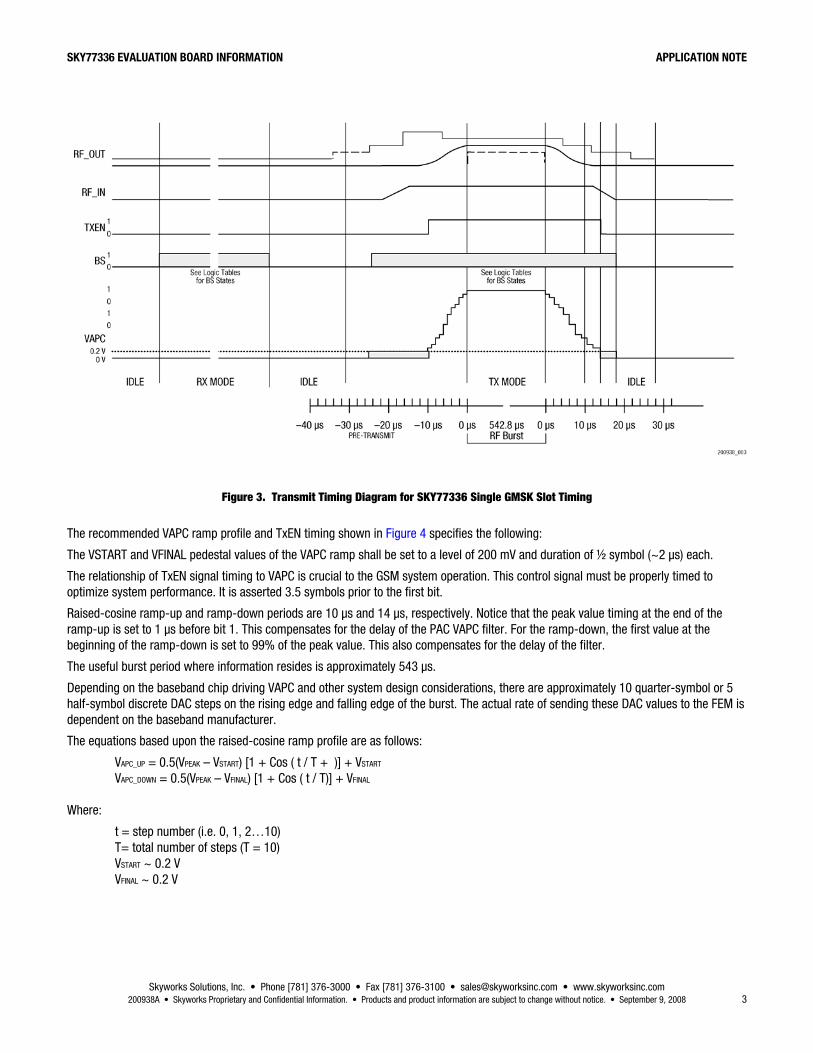
Timing of the burst is critical to handset performance as it directly affects the time mask and switching transients. To optimize handset performance, Skyworks strongly recommends the timing diagram in Figure 3.
SKY77336 EVALUATION BOARD INFORMATION APPLICATION NOTE
Skyworks Solutions, Inc. • Phone [781] 376-3000 • Fax [781] 376-3100 • [email protected] • www.skyworksinc.com 200938A • Skyworks Proprietary and Confidential Information. • Products and product information are subject to change without notice. • September 9, 2008 3
Figure 3. Transmit Timing Diagram for SKY77336 Single GMSK Slot Timing
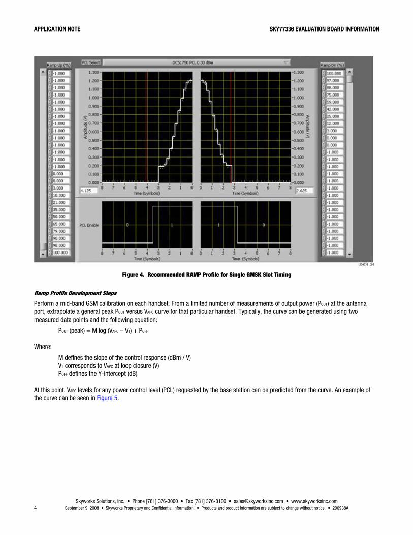
The recommended VAPC ramp profile and TxEN timing shown in Figure 4 specifies the following:
The VSTART and VFINAL pedestal values of the VAPC ramp shall be set to a level of 200 mV and duration of ½ symbol (~2 μs) each.
The relationship of TxEN signal timing to VAPC is crucial to the GSM system operation. This control signal must be properly timed to optimize system performance. It is asserted 3.5 symbols prior to the first bit.
Raised-cosine ramp-up and ramp-down periods are 10 μs and 14 μs, respectively. Notice that the peak value timing at the end of the ramp-up is set to 1 μs before bit 1. This compensates for the delay of the PAC VAPC filter. For the ramp-down, the first value at the beginning of the ramp-down is set to 99% of the peak value. This also compensates for the delay of the filter.
The useful burst period where information resides is approximately 543 μs.
Depending on the baseband chip driving VAPC and other system design considerations, there are approximately 10 quarter-symbol or 5 half-symbol discrete DAC steps on the rising edge and falling edge of the burst. The actual rate of sending these DAC values to the FEM is dependent on the baseband manufacturer.
The equations based upon the raised-cosine ramp profile are as follows:
VAPC_UP = 0.5(VPEAK – VSTART) [1 + Cos ( t / T + )] + VSTART VAPC_DOWN = 0.5(VPEAK – VFINAL) [1 + Cos ( t / T)] + VFINAL
Where:
t = step number (i.e. 0, 1, 2…10) T= total number of steps (T = 10) VSTART ~ 0.2 V VFINAL ~ 0.2 V
APPLICATION NOTE SKY77336 EVALUATION BOARD INFORMATION
Skyworks Solutions, Inc. • Phone [781] 376-3000 • Fax [781] 376-3100 • [email protected] • www.skyworksinc.com 4 September 9, 2008 • Skyworks Proprietary and Confidential Information. • Products and product information are subject to change without notice. • 200938A
Figure 4. Recommended RAMP Profile for Single GMSK Slot Timing
Ramp Profile Development Steps
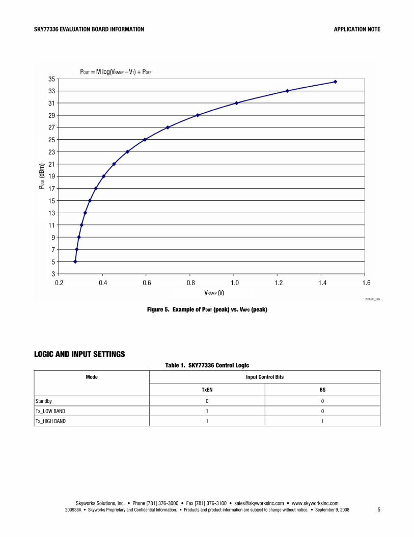
Perform a mid-band GSM calibration on each handset. From a limited number of measurements of output power (POUT) at the antenna port, extrapolate a general peak POUT versus VAPC curve for that particular handset. Typically, the curve can be generated using two measured data points and the following equation:
POUT (peak) = M log (VAPC – VT) + POFF
Where:
M defines the slope of the control response (dBm / V) VT corresponds to VAPC at loop closure (V) POFF defines the Y-intercept (dB)
At this point, VAPC levels for any power control level (PCL) requested by the base station can be predicted from the curve. An example of the curve can be seen in Figure 5.
SKY77336 EVALUATION BOARD INFORMATION APPLICATION NOTE
Skyworks Solutions, Inc. • Phone [781] 376-3000 • Fax [781] 376-3100 • [email protected] • www.skyworksinc.com 200938A • Skyworks Proprietary and Confidential Information. • Products and product information are subject to change without notice. • September 9, 2008 5
Figure 5. Example of POUT (peak) vs. VAPC (peak)
LOGIC AND INPUT SETTINGS Table 1. SKY77336 Control Logic
Input Control Bits Mode
TxEN BS
Standby 0 0
Tx_LOW BAND 1 0
Tx_HIGH BAND 1 1
APPLICATION NOTE SKY77336 EVALUATION BOARD INFORMATION
Skyworks Solutions, Inc. • Phone [781] 376-3000 • Fax [781] 376-3100 • [email protected] • www.skyworksinc.com 6 September 9, 2008 • Skyworks Proprietary and Confidential Information. • Products and product information are subject to change without notice. • 200938A
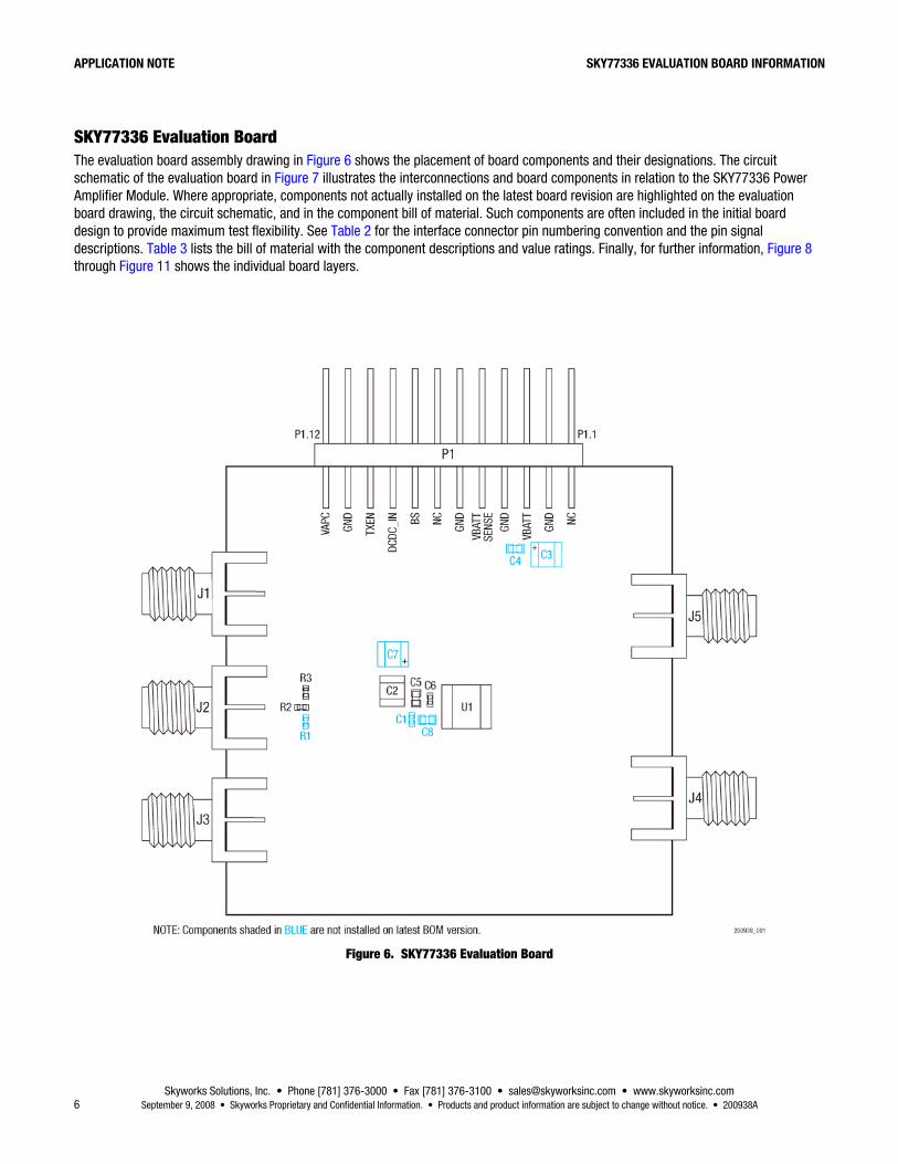
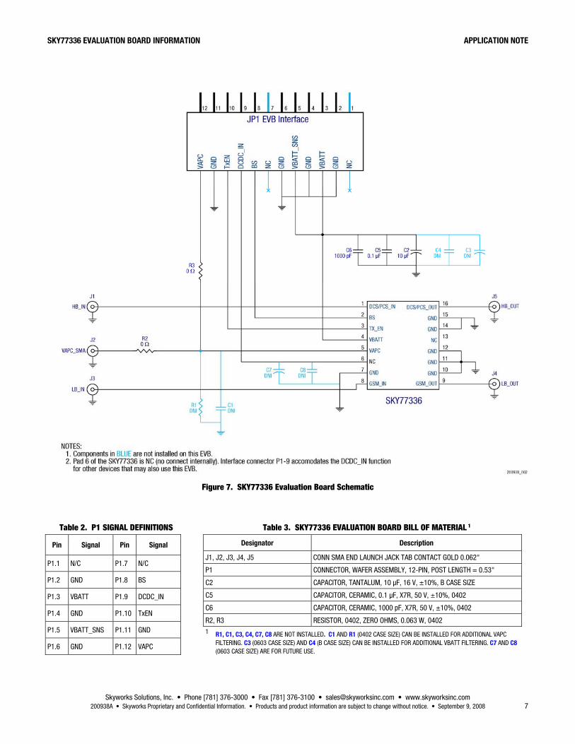
SKY77336 Evaluation Board The evaluation board assembly drawing in Figure 6 shows the placement of board components and their designations. The circuit schematic of the evaluation board in Figure 7 illustrates the interconnections and board components in relation to the SKY77336 Power Amplifier Module. Where appropriate, components not actually installed on the latest board revision are highlighted on the evaluation board drawing, the circuit schematic, and in the component bill of material. Such components are often included in the initial board design to provide maximum test flexibility. See Table 2 for the interface connector pin numbering convention and the pin signal descriptions. Table 3 lists the bill of material with the component descriptions and value ratings. Finally, for further information, Figure 8 through Figure 11 shows the individual board layers.
Figure 6. SKY77336 Evaluation Board
SKY77336 EVALUATION BOARD INFORMATION APPLICATION NOTE
Skyworks Solutions, Inc. • Phone [781] 376-3000 • Fax [781] 376-3100 • [email protected] • www.skyworksinc.com 200938A • Skyworks Proprietary and Confidential Information. • Products and product information are subject to change without notice. • September 9, 2008 7
Figure 7. SKY77336 Evaluation Board Schematic
Table 2. P1 SIGNAL DEFINITIONS
Pin Signal Pin Signal
P1.1 N/C P1.7 N/C
P1.2 GND P1.8 BS
P1.3 VBATT P1.9 DCDC_IN
P1.4 GND P1.10 TxEN
P1.5 VBATT_SNS P1.11 GND
P1.6 GND P1.12 VAPC
Table 3. SKY77336 EVALUATION BOARD BILL OF MATERIAL 1
Designator Description
J1, J2, J3, J4, J5 CONN SMA END LAUNCH JACK TAB CONTACT GOLD 0.062"
P1 CONNECTOR, WAFER ASSEMBLY, 12-PIN, POST LENGTH = 0.53"
C2 CAPACITOR, TANTALUM, 10 μF, 16 V, ±10%, B CASE SIZE
C5 CAPACITOR, CERAMIC, 0.1 μF, X7R, 50 V, ±10%, 0402
C6 CAPACITOR, CERAMIC, 1000 pF, X7R, 50 V, ±10%, 0402
R2, R3 RESISTOR, 0402, ZERO OHMS, 0.063 W, 0402
1 R1, C1, C3, C4, C7, C8 ARE NOT INSTALLED. C1 AND R1 (0402 CASE SIZE) CAN BE INSTALLED FOR ADDITIONAL VAPC FILTERING. C3 (0603 CASE SIZE) AND C4 (B CASE SIZE) CAN BE INSTALLED FOR ADDITIONAL VBATT FILTERING. C7 AND C8 (0603 CASE SIZE) ARE FOR FUTURE USE.
SKY77336 EVALUATION BOARD INFORMATION APPLICATION NOTE
Skyworks Solutions, Inc. • Phone [781] 376-3000 • Fax [781] 376-3100 • [email protected] • www.skyworksinc.com 200938A • Skyworks Proprietary and Confidential information. • Products and product information are subject to change without notice. • September 8, 2008 8
Figure 8. SKY77336 Evaluation Board Layer 1
SKY77336 EVALUATION BOARD INFORMATION APPLICATION NOTE
Skyworks Solutions, Inc. • Phone [781] 376-3000 • Fax [781] 376-3100 • [email protected] • www.skyworksinc.com 200938A • Skyworks Proprietary and Confidential Information. • Products and product information are subject to change without notice. • September 9, 2008 9
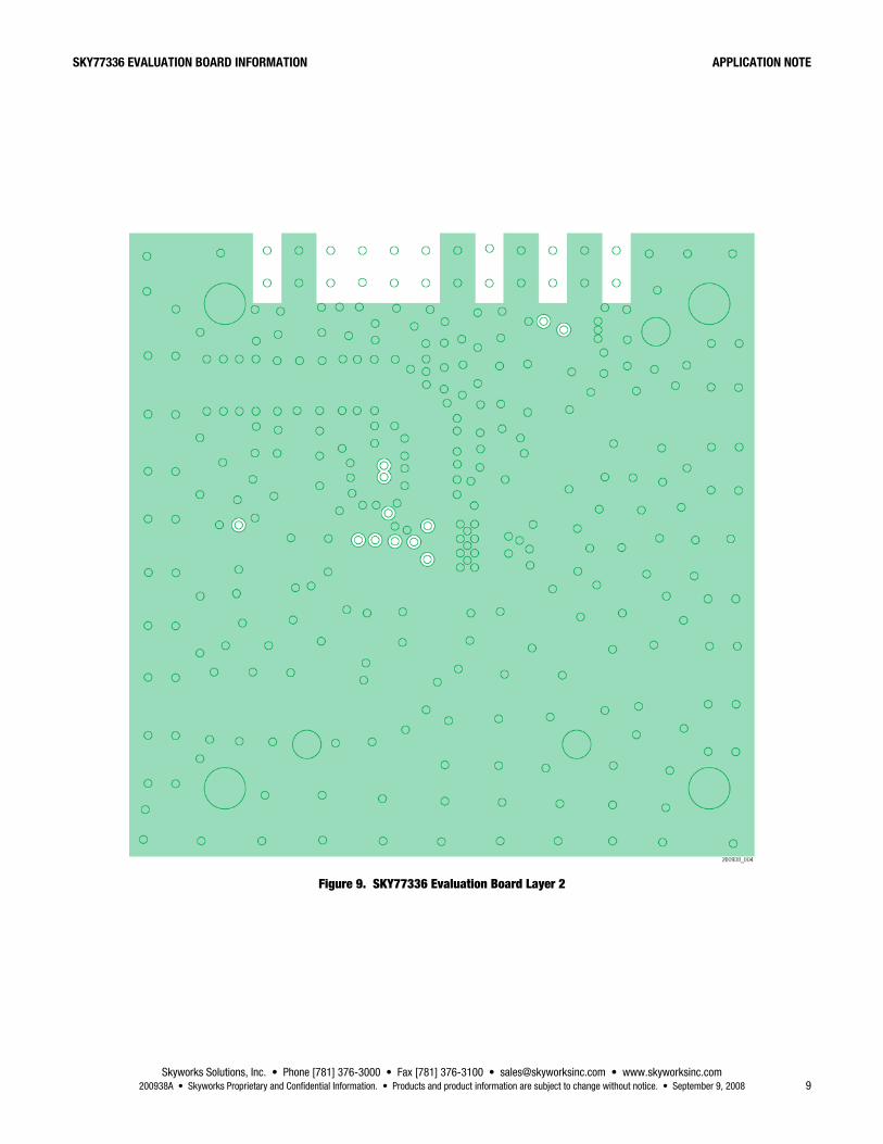
Figure 9. SKY77336 Evaluation Board Layer 2
APPLICATION NOTE SKY77336 EVALUATION BOARD INFORMATION
Skyworks Solutions, Inc. • Phone [781] 376-3000 • Fax [781] 376-3100 • [email protected] • www.skyworksinc.com 10 September 9, 2008 • Skyworks Proprietary and Confidential Information. • Products and product information are subject to change without notice. • 200938A
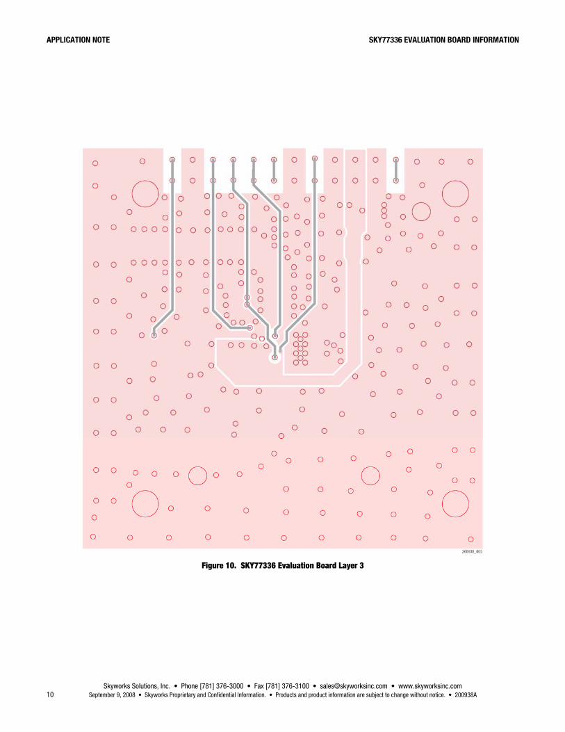
Figure 10. SKY77336 Evaluation Board Layer 3
SKY77336 EVALUATION BOARD INFORMATION APPLICATION NOTE
Skyworks Solutions, Inc. • Phone [781] 376-3000 • Fax [781] 376-3100 • [email protected] • www.skyworksinc.com 200938A • Skyworks Proprietary and Confidential Information. • Products and product information are subject to change without notice. • September 9, 2008 11
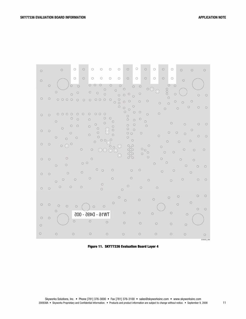
Figure 11. SKY77336 Evaluation Board Layer 4
APPLICATION NOTE SKY77336 EVALUATION BOARD INFORMATION
Skyworks Solutions, Inc. • Phone [781] 376-3000 • Fax [781] 376-3100 • [email protected] • www.skyworksinc.com 12 September 9, 2008 • Skyworks Proprietary and Confidential Information. • Products and product information are subject to change without notice. • 200938A
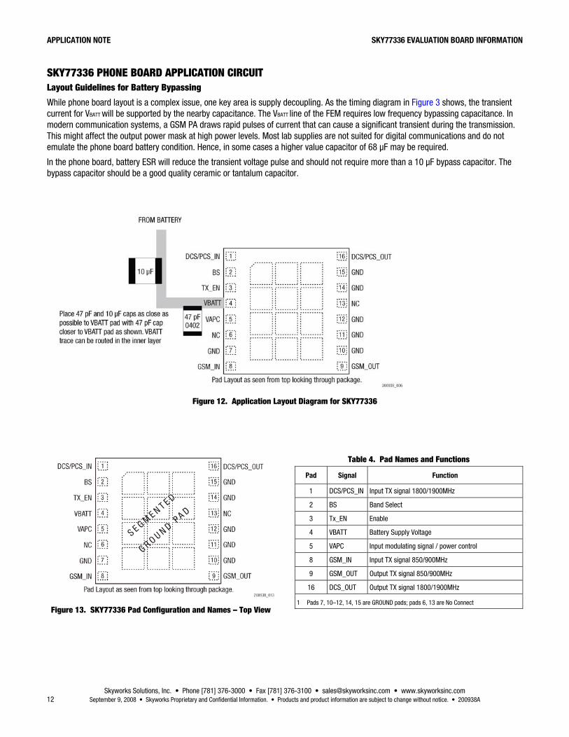
SKY77336 PHONE BOARD APPLICATION CIRCUIT Layout Guidelines for Battery Bypassing
While phone board layout is a complex issue, one key area is supply decoupling. As the timing diagram in Figure 3 shows, the transient current for VBATT will be supported by the nearby capacitance. The VBATT line of the FEM requires low frequency bypassing capacitance. In modern communication systems, a GSM PA draws rapid pulses of current that can cause a significant transient during the transmission. This might affect the output power mask at high power levels. Most lab supplies are not suited for digital communications and do not emulate the phone board battery condition. Hence, in some cases a higher value capacitor of 68 μF may be required.
In the phone board, battery ESR will reduce the transient voltage pulse and should not require more than a 10 μF bypass capacitor. The bypass capacitor should be a good quality ceramic or tantalum capacitor.
Figure 12. Application Layout Diagram for SKY77336
Figure 13. SKY77336 Pad Configuration and Names – Top View
Table 4. Pad Names and Functions
Pad Signal Function
1 DCS/PCS_IN Input TX signal 1800/1900MHz
2 BS Band Select
3 Tx_EN Enable
4 VBATT Battery Supply Voltage
5 VAPC Input modulating signal / power control
8 GSM_IN Input TX signal 850/900MHz
9 GSM_OUT Output TX signal 850/900MHz
16 DCS_OUT Output TX signal 1800/1900MHz
1 Pads 7, 10–12, 14, 15 are GROUND pads; pads 6, 13 are No Connect
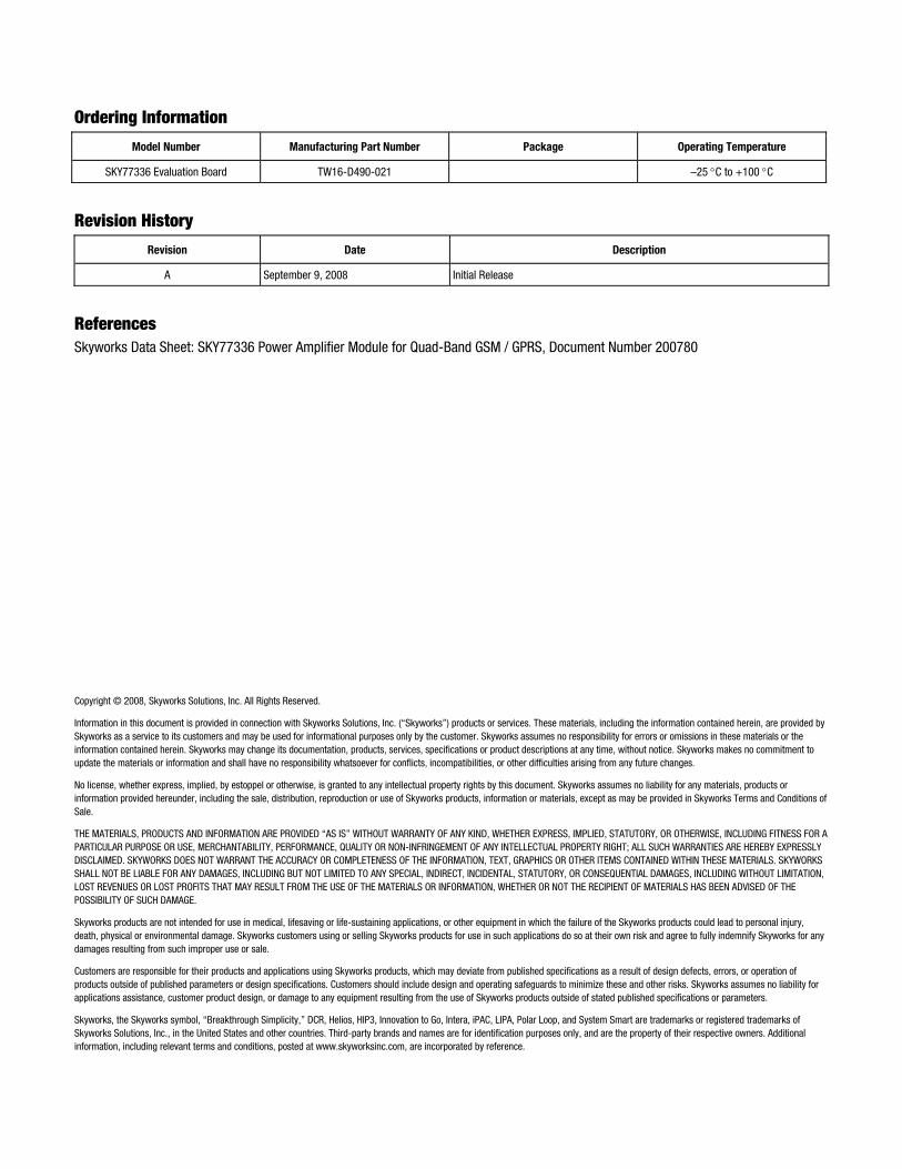
Ordering Information
Model Number Manufacturing Part Number Package Operating Temperature
SKY77336 Evaluation Board TW16-D490-021 –25 °C to +100 °C
Revision History
Revision Date Description
A September 9, 2008 Initial Release
References Skyworks Data Sheet: SKY77336 Power Amplifier Module for Quad-Band GSM / GPRS, Document Number 200780
Copyright © 2008, Skyworks Solutions, Inc. All Rights Reserved.
Information in this document is provided in connection with Skyworks Solutions, Inc. (“Skyworks”) products or services. These materials, including the information contained herein, are provided by Skyworks as a service to its customers and may be used for informational purposes only by the customer. Skyworks assumes no responsibility for errors or omissions in these materials or the information contained herein. Skyworks may change its documentation, products, services, specifications or product descriptions at any time, without notice. Skyworks makes no commitment to update the materials or information and shall have no responsibility whatsoever for conflicts, incompatibilities, or other difficulties arising from any future changes.
No license, whether express, implied, by estoppel or otherwise, is granted to any intellectual property rights by this document. Skyworks assumes no liability for any materials, products or information provided hereunder, including the sale, distribution, reproduction or use of Skyworks products, information or materials, except as may be provided in Skyworks Terms and Conditions of Sale.
THE MATERIALS, PRODUCTS AND INFORMATION ARE PROVIDED “AS IS” WITHOUT WARRANTY OF ANY KIND, WHETHER EXPRESS, IMPLIED, STATUTORY, OR OTHERWISE, INCLUDING FITNESS FOR A PARTICULAR PURPOSE OR USE, MERCHANTABILITY, PERFORMANCE, QUALITY OR NON-INFRINGEMENT OF ANY INTELLECTUAL PROPERTY RIGHT; ALL SUCH WARRANTIES ARE HEREBY EXPRESSLY DISCLAIMED. SKYWORKS DOES NOT WARRANT THE ACCURACY OR COMPLETENESS OF THE INFORMATION, TEXT, GRAPHICS OR OTHER ITEMS CONTAINED WITHIN THESE MATERIALS. SKYWORKS SHALL NOT BE LIABLE FOR ANY DAMAGES, INCLUDING BUT NOT LIMITED TO ANY SPECIAL, INDIRECT, INCIDENTAL, STATUTORY, OR CONSEQUENTIAL DAMAGES, INCLUDING WITHOUT LIMITATION, LOST REVENUES OR LOST PROFITS THAT MAY RESULT FROM THE USE OF THE MATERIALS OR INFORMATION, WHETHER OR NOT THE RECIPIENT OF MATERIALS HAS BEEN ADVISED OF THE POSSIBILITY OF SUCH DAMAGE.
Skyworks products are not intended for use in medical, lifesaving or life-sustaining applications, or other equipment in which the failure of the Skyworks products could lead to personal injury, death, physical or environmental damage. Skyworks customers using or selling Skyworks products for use in such applications do so at their own risk and agree to fully indemnify Skyworks for any damages resulting from such improper use or sale.
Customers are responsible for their products and applications using Skyworks products, which may deviate from published specifications as a result of design defects, errors, or operation of products outside of published parameters or design specifications. Customers should include design and operating safeguards to minimize these and other risks. Skyworks assumes no liability for applications assistance, customer product design, or damage to any equipment resulting from the use of Skyworks products outside of stated published specifications or parameters.
Skyworks, the Skyworks symbol, “Breakthrough Simplicity,” DCR, Helios, HIP3, Innovation to Go, Intera, iPAC, LIPA, Polar Loop, and System Smart are trademarks or registered trademarks of Skyworks Solutions, Inc., in the United States and other countries. Third-party brands and names are for identification purposes only, and are the property of their respective owners. Additional information, including relevant terms and conditions, posted at www.skyworksinc.com, are incorporated by reference.