multiband lte power amplifier for handset...
TRANSCRIPT
MULTIBAND LTE POWER AMPLIFIER FOR HANDSET
APPLICATION
JAGADHESWARAN RAJENDRAN
THESIS SUBMITTED IN FULFILMENT OF THE REQUIREMENT
FOR THE DEGREE OF DOCTOR OF PHILOSOPHY IN
ENGINEERING
FACULTY OF ENGINEERING
UNIVERSITY OF MALAYA
KUALA LUMPUR
2015
iii
ABSTRACT
As wireless communication standard continues to evolve accommodating the demand of
high data rate operation, the design of RF power amplifier (PA) becomes ever challenging.
PAs are required to operate more efficiently while maintaining stringent linearity
requirement. In this work, a new circuit to extend the linear operation bandwidth of a LTE
(Long Term Evolution) power amplifier, while delivering a high efficiency is presented.
The 950µm x 900µm monolithic microwave integrated circuit (MMIC) power amplifier
(PA) is fabricated in a 2µm InGaP/GaAs process. The PA consists of three stages, which is
the pre-driver, driver and main stages. The main stage is designed in class-J configuration
in order to improve the efficiency of the PA. The optimum conduction angle method is
employed to enable the PA to operate in bias condition which has the optimum operation
for linearity and efficiency. A novel on-chip analog pre-distorter (APD) is designed and
integrated into the driver stage to improve the linearity of the highly efficient PA further to
meet the adjacent channel leakage ratio (ACLR) and error vector magnitude (EVM)
specifications for LTE signal profile with 20MHz channel bandwidth. Experimental result
verifies that the designed PA is capable to meet the ACLR specifications of -30dBc from
1.7GHz to 2.05GHz which encapsulates LTE Band 1,2,3,4,9,10,33,34,35,36,37 and 39 at
maximum linear output power of 28dBm. The maximum EVM at 28dBm for 16-QAM
scheme is 3.38% at 2050MHz.The corresponding power added efficiency (PAE) varies
from 40.5% to 55.8% across band. With a respective input return loss of less than -15dB,
the PA’s maximum power gain is measured to be 35.8dB while exhibiting an unconditional
stability characteristic from DC up to 5GHz. The proposed architecture serves to be a good
solution to improve the linearity and efficiency of a PA for wideband LTE operation

iv
without sacrificing other critical performance metrics. This will ultimately reach the goal to
have single chip solution for handset LTE PA.

v
ABSTRAK
Sebagai wayarles komunikasi standard terus berkembang menampung permintaan operasi
kadar data yang tinggi , reka bentuk RF penguat kuasa (PA) menjadi semakin mencabar.
PA diperlukan untuk beroperasi dengan lebih cekap di samping mengekalkan keperluan
kelinearan ketat. Dalam karya ini , litar baru untuk melanjutkan jalur lebar operasi linear
daripada LTE ( Long Term Evolution ) penguat kuasa, manakala menyampaikan kecekapan
yang tinggi dibentangkan. X 900μm mikro litar bersepadu monolitik 950μm (MMIC )
amplifier kuasa ( PA) adalah rekaan dalam 2μm InGaP / GaAs proses. PA ini terdiri
daripada tiga peringkat , yang merupakan pra- pemandu, pemandu dan peringkat utama.
Pentas utama direka dalam konfigurasi kelas -J untuk meningkatkan kecekapan PA tanpa
perdagangan teruk off dalam keupayaan penghantaran linear . Novel A atas cip analog pra-
distorter (APD ) direka dan bersepadu ke peringkat pemandu untuk meningkatkan
kelinearan PA yang sangat berkesan untuk memenuhi nisbah bersebelahan saluran
kebocoran (PPHT) dan vektor magnitud ralat ( EVM ) spesifikasi untuk isyarat LTE profil
dengan saluran jalur lebar 20MHz . Hasil eksperimen mengesahkan bahawa PA yang
direka mampu untuk memenuhi spesifikasi PPHT of- 30dBc dari 1.7GHz untuk 2.05GHz
yang merangkumi LTE Band 1,2,3,4,9,10,33,34,35,36,37 dan 39 pada kuasa output linear
maksimum 28dBm . The EVM maksimum pada 28dBm untuk skim 16- QAM adalah 3.38
% pada 2050MHz.The kuasa sama menambah kecekapan ( PAE ) berbeza daripada 40.5%
kepada 55.8 % di seluruh band. Dengan input kerugian pulangan masing-masing kurang
daripada- 15dB , keuntungan kuasa maksimum PA adalah diukur untuk menjadi 35.8dB
manakala mempamerkan satu ciri kestabilan tanpa syarat dari DC sehingga 5GHz . Seni
bina yang dicadangkan bertujuan untuk menjadi satu penyelesaian yang baik untuk

vi
meningkatkan kelinearan dan kecekapan PA untuk operasi LTE Wideband tanpa
mengorbankan lain metrik prestasi kritikal. Ini akhirnya akan mencapai matlamat untuk
mempunyai penyelesaian cip tunggal untuk telefon bimbit LTE PA.

vii
ACKNOWLEDGEMENTS
I first would like to express my deepest gratitude to my supervisor, Dr Harikrishnan
Ramiah for his dedicated supervision and invaluable guidance on my research project. His
enthusiasm and motivation drove me throughout this project. His vision and strong
technical knowledge is a major contributor to the successful completion of this project.
Thank you very much Dr Hari.
I also would like to thank the Higher Education Ministry of Malaysia for providing
me the financial support through the MyPhD Scholarship. This work would not have been
possible without this support.
Finally, I would like to express my deepest gratitude to my wife Mrs Kavitha
Jagadheswaran for her endless love and support throughout this project. I am also grateful
to my parents Mr Rajendran Uthirajoo and Mrs Suppamah Govindasamy for their
continuous encouragement during the tough times. Last but not least, I would like to thank
my lovely daughter, Tharini Jagadheswaran for her smiles and laughter which encourages
me to always stay positive and cheerful.

viii
TABLE OF CONTENTS
ABSTRACT iii
ABSTRAK v
ACKNOWLEDGEMENTS vii
LIST OF FIGURES xii
LIST OF TABLES xvii
LIST OF ABBREVIATIONS xviii
LIST OF APPENDICES xix
CHAPTER 1. INTRODUCTION 1
1.1 Overview of LTE Systems 1
1.2 Research Motivation 5
1.3 Research Objectives 7
1.4 Thesis Organization 8
CHAPTER 2. LITERATURE REVIEW OF POWER AMPLIFIER EFFICIENCY
AND LINEARIZATION TECHNIQUES 9
2.1 Introduction 9
2.2 Efficiency Enhancement Techniques 10
2.2.1 Device Switching 10

ix
2.2.2 Doherty Power Amplifier 11
2.2.3 Average Bias Tracking 14
2.2.4 Envelope Tracking 15
2.2.5 Class-S 18
2.3 Linearization Techniques 18
2.3.1 Hybrid Class PA 18
2.3.2 Feedforward Linearization Technique 19
2.3.3 Analog Pre-Distortion Linearization 21
2.3.4 Digital Pre-Distortion Linearization 23
2.3.5 Other Linearization Techniques 23
2.4 Process Evolution in RFPA Design 25
CHAPTER 3. POWER CELL DESIGN 26
3.1 Introduction 26
3.2 Power Cell Optimum Size 26
3.3 Thermal Runaway Phenomenon 37
3.3.1Thermal Runaway in HBT 37
3.3.2 Thermal Compensation Circuit 40
3.3.3 Measurement Evaluation 44
3.4 Power Cell Optimum Conduction Angle 49
3.4.1 Fourier Analysis 49
x
3.4.2 Relationship between Conduction Angle and Efficiency 53
3.4.3 Optimum Bias Point Determination 55
3.5 Biasing Circuit Design 57
CHAPTER 4. DESIGN OF WIDEBAND EFFICIENCY POWER AMPLIFIER 59
4.1 Introduction 59
4.2 Class-J Power Amplifier- Theoretical Analysis 61
4.2.1 Fundamental of Class-J Design 61
4.2.2 Class-J Output Impedance Analysis with the Integration of Output Matching
Network 67
4.3 Simulation Analysis 70
4.4 Output Matching Network Design 73
CHAPTER 5. ANALOG PRE-DISTORTER DESIGN AND THE REALIZATION OF
HIGH GAIN POWER AMPLIFIER 80
5.1 Introduction 80
5.2 Theoretical Analysis of APD Technique 81
5.3 APD Design Methodologies 85
5.3.1 Initial Design Methodologies 85
5.3.1.1 Passive Pre-Distorter Linearizer 85
5.3.1.2 Dual Stage Linearizer 87
5.3.2 Novel Wideband APD 89

xi
5.4 High Gain Power Amplifier Design 96
CHAPTER 6. MEASUREMENT RESULTS 98
6.1 Measurement Station Setup 98
6.2 Measurement Results 101
6.2.1 Small Signal Measurement Results 101
6.2.2 Large Signal Measurement Results 103
CHAPTER 7. CONCLUSION AND FUTURE WORKS 116
7.1 Conclusion 116
7.2 Future Works 118
REFERENCES 119
LIST OF PUBLICATIONS AND PAPERS PRESENTED 128
APPENDIX A 137
APPENDIX B 141
APPENDIX C 145

xii
LIST OF FIGURES
Figure 1.1: LTE Bands around the Globe…………………………………………………...3
Figure 1.2: OFDMA and SC-FDMA Comparison in Transmitting QPSK Symbols………..4
Figure 1.3: Tear down of a Smart Phone……………………………………………………6
Figure 2.1: Switching PA Topology…………………………………………………….....11
Figure 2.2: DPA Concept………………………………………………………………......12
Figure 2.3: DPA Topology…………………………………………………………………13
Figure 2.4: DPA Profile……………………………………………………………………13
Figure 2.5: ET Topology…………………………………………………………………...16
Figure 2.6: Feedforward Transmitter Block Diagram……………………………………...19
Figure 2.7: Analog Predistortion Technique……………………………………………….22
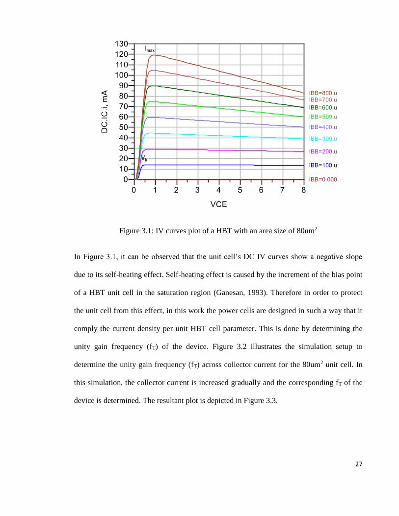
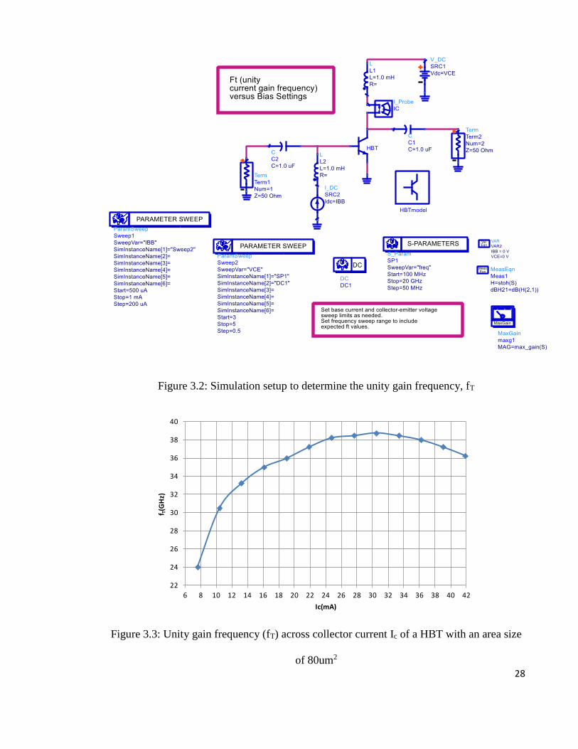
Figure 3.1: IV Curves Plot of a HBT with an Area Size of 80um2………………………...27
Figure 3.2: Simulation Setup to Determine the Unity Gain Frequency, fT………………...28
Figure 3.3: Unity Gain Frequency (fT) Across Collector Current Ic of a HBT with an Area
size of 80um2…………………………………………………………………...28
Figure 3.4: Power cell of the LTE PA……………………………………………………...32
Figure 3.5: Simulation setup to measure the maximum output power and efficiency of the
power cell………………………………………………………………………33
Figure 3.6: Simulation Result for the 4800um2 Power Cell with Load
Resistance of 3.33Ω……………………………………………………………34
Figure 3.7: Load Line Swing across Collector Voltage of the Power Cell up to Maximum
Output Power of 33dBm………………………………………………………..35

xiii
Figure 3.8: The load resistance Rload is swept from 3Ω to 5Ω, in 0.5Ω step………………36
Figure 3.9: HBT unit cells in parallel………………………………………………………38
Figure 3.10: Current collapse phenomenon observed in Device 2, represented by Icc2……38
Figure 3.11: Device 1 is experiencing Vbe degradation, which is indication of thermal
runaway phenomenon………………………………………………………...39
Figure 3.12: Strap resistor, Rss1 and Rss2 are implemented mitigating thermal runaway
phenomenon…………………………………………………………………...41
Figure 3.13: (a) The schematic in Figure 3.9 is redrawn with strap resistors integrated at the
base of the transistors……………………………………………………...43
Figure 3.13: (b) Collector current in Device 1, Icc1 and Device 2, Icc2 do not collapse after
integration of strap resistors……………………………………………...44
Figure 3.14: Micrograph of PA fabricated with strap resistors…………………………….45
Figure 3.15: Schematic of the fabricated PA with strap resistors integration……………...45
Figure 3.16: AM-AM comparison plot of the PA with base ballast and strap ballast……..46
Figure 3.17: Collector current (Icc) against output power comparison in base ballast and
strap resistor integration……………………………………………………….47
Figure 3.18: LTE ACLR plots comparing three different combinations…………………..48
Figure 3.19: The PAE comparison plot across output power for both techniques…………48
Figure 3.20: The collector current waveform plot…………………………………………50
Figure 3.21: Current waveform’s normalized amplitude across conduction angle………...52
Figure 3.22: Collector current waveforms for various conduction angle of the PA……….54
Figure 3.23: Single stage power amplifier for the optimum bias point determination ……55
Figure 3.24: Measurement Setup…………………………………………………………..56
xiv
Figure 3.25: ACLR and PAE plot for various biasing current for the single stage
amplifier……………………………………………………………………...56
Figure 3.26: Proposed biasing circuit………………………………………………………58
Figure 4.1: The voltage and current waveform of various classes of PA………………….60
Figure 4.2: The modification of the voltage waveform……………………………………64
Figure 4.3: The schematic of class-J HBT PA……………………………………………..67
Figure 4.4: Class-J amplifier load pull simulation setup…………………………………...71
Figure 4.5: Gain and PAE plot across output power for Zout 2+j3…………………………72
Figure 4.6: Output matching network topology of the class-J amplifier…………………..73
Figure 4.7: Impedance Transformation Plot……………………………………………….75
Figure 4.8: The simulated output power and PAE of the fully modeled final stage class-J
amplifier……………………………………………………………………….77
Figure 4.9: Class-J Output impedance and second harmonic plot across output power from
1.7GHz to 2GHz………………………………………………………….......77
Figure 4.10: Class-J voltage and current waveform at Psat and Pbo of 28dBm……………..78
Figure 5.1: Nonlinear amplification of PA………………………………………………...81
Figure 5.2: The resultant third order frequency components generated due to amplification
of dual carrier signals ω1 and ω2……………………………………………....82
Figure 5.3: Interference component generated by ω3 to ω1………………………………...83
Figure 5.4: IMD3 cancellation analysis……………………………………………………83
Figure 5.5: Proposed class-E LTE PA with passive pre-distorter………………………….85
Figure 5.6: Measured AM-AM responses of the Class-E PA before and
after linearization……………………………………………………………....86
xv
Figure 5.7: Simulated spectrum of the PA at 1.95 GHz……………………………………86
Figure 5.8: The schematic of the proposed PA with integrated dual stage linearizer
network..............................................................................................................87
Figure 5.9: Measured ACLR comparison between PA with and without dual stage
linearizer at 1980MHz…………………………………...................................88
Figure 5.10: Schematic diagram of the LTE PA with built in APD……………………….89
Figure 5.11: Load pull simulation result which illustrates the IMD3 and PAE contours of
the main amplifier at output power 28dBm…….............................................90
Figure 5.12: Biasing profile of the integrated parallel base collector diodes……………....92
Figure 5.13: Simulated AM-PM responses of the APD and main amplifier across operating
band………………………………………………………………………......93
Figure 5.14: Location of the impedance point of the driver (A), main amplifier (B) and
APD(X) at centre frequency of 1.7GHz……………………………………...94
Figure 5.15: AM-AM profile for various intermediate matching network impedances
mentioned in Figure 5.14…………………………………………………….94
Figure 5.16: IMD3 and PAE contours of the PA after linearization……………………….95
Figure 6.1: Small signal Measurement Setup…………………………………………….99
Figure 6.2: Large Signal Measurement Setup…………………………………………….99
Figure 6.3: Die microphotograph of the fabricated PA with integrated APD…………….100
Figure 6.4: Measured and simulated S-parameters of the PA with supply headroom of
3.3V……………………..................................................................................101
Figure 6.5: PA has K-Factor >1 from DC up to 5GHz…………………………………...102
Figure 6.6: Source and load stability circles……………………………………………...102
xvi
Figure 6.7: Power gain plot across output power………………………………………..103
Figure 6.8: CCDF curve of the 20MHz 16QAM LTE signal…………………………...104
Figure 6.9: ACLR and PAE performances of the linearized PA from 1.7GHz to
2.05GHz……………………………………………………………….........105
Figure 6.10: ACLR and spectral mask at output power of 28dBm from 1.71GHz to
2.05GHz which are within the specifications……….....................................105
Figure 6.11: EVM plot of the linearized PA……………………………………………...110
Figure 6.12: EVM constellation diagram at output power of 28dBm from 1.71GHz to
2.05GHz which are within the specifications……………….........................110

xvii
LIST OF TABLES
Table 1.1: LTE Frequency Bands ……..……………………………………………………3
Table 2.1: Performance Comparison of Various Topologies ...............................................24
Table 3.1: Conduction angle and corresponding quiescent current for a typical class-A, AB
and B amplifier ...................................................................................................54
Table 6.1: Performance summary of the PA……………………………...........................113
Table 6.2: Performance comparison of published LTE power amplifiers………..............114
xviii
LIST OF ABBREVIATIONS
ACLR Adjacent Channel Leakage Ratio
APD Analog Pre-Distorter
EVM Error Vector Magnitude
IMD3 Third Order Intermodulation Product
LTE Long Term Evolution
OFDMA Orthogonal Frequency Division Multiple
Access
PA Power Amplifier
PAPR Peak to Average Power Ratio
QAM Quadrature Amplitude Modulation
SC-FDMA Single Carrier Frequency Division Multiple
Access

xix
LIST OF APPENDICES
Appendix A- Reduced Conduction Angle Analysis……………………………………...137
Appendix B- Class-J Power Amplifier Fundamental and Second Order Voltage Analysis
………………….141
Appendix C- Class-J Output Matching Network Analysis……………………………….145
1
CHAPTER 1. INTRODUCTION
1.1 Overview of LTE System
Long Term Evolution (LTE) evolves from the Universal Mobile Telephone System
(UMTS) which was initiated by the Third Generation Partnership Project (3GPP) to address
the continuous demand for high data rates. Among the key specifications of LTE are
(Rumney, LTE Introduction, 2009):
a) Increased downlink and uplink peak data rates.
b) Scalable channel bandwidths of 1.4MHz, 3.0MHz, 5MHz, 10MHz, 15MHz and
20MHz in both uplink and downlink.
c) Spectral efficiency improvements over Release 6 HSPA of 3 to 4 times in the
downlink and 2 to 3 times in the uplink.
d) Sub- 5ms latency for small Internet Protocol (IP) packets.
e) Performance optimized for low mobile speeds from 0 to 15km/h supported with
high performance from 15 to 120km/h; functional support from 120 to 350km/h.
f) Co-existence with legacy standards while evolving toward an all-IP network.
The LTE frequency bands as defined by the European Telecommunications Standards
Institute (ETSI) and 3GPP are shown in Table 1.1 (3GPP TS 36.101 version 9.4.0 Release
9, 2010).
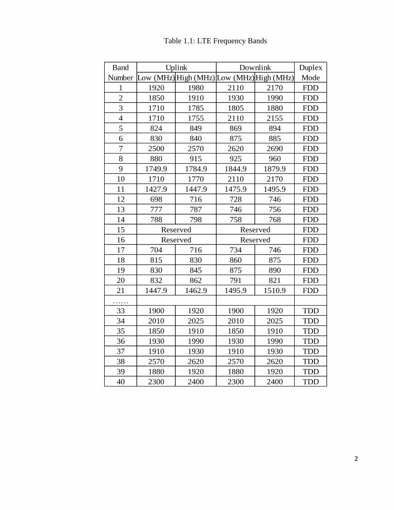
2
Table 1.1: LTE Frequency Bands
Low (MHz) High (MHz) Low (MHz)High (MHz)
1 1920 1980 2110 2170 FDD
2 1850 1910 1930 1990 FDD
3 1710 1785 1805 1880 FDD
4 1710 1755 2110 2155 FDD
5 824 849 869 894 FDD
6 830 840 875 885 FDD
7 2500 2570 2620 2690 FDD
8 880 915 925 960 FDD
9 1749.9 1784.9 1844.9 1879.9 FDD
10 1710 1770 2110 2170 FDD
11 1427.9 1447.9 1475.9 1495.9 FDD
12 698 716 728 746 FDD
13 777 787 746 756 FDD
14 788 798 758 768 FDD
15 FDD
16 FDD
17 704 716 734 746 FDD
18 815 830 860 875 FDD
19 830 845 875 890 FDD
20 832 862 791 821 FDD
21 1447.9 1462.9 1495.9 1510.9 FDD
……
33 1900 1920 1900 1920 TDD
34 2010 2025 2010 2025 TDD
35 1850 1910 1850 1910 TDD
36 1930 1990 1930 1990 TDD
37 1910 1930 1910 1930 TDD
38 2570 2620 2570 2620 TDD
39 1880 1920 1880 1920 TDD
40 2300 2400 2300 2400 TDD
Band
Number
Uplink Downlink Duplex
Mode
Reserved Reserved
Reserved Reserved
3
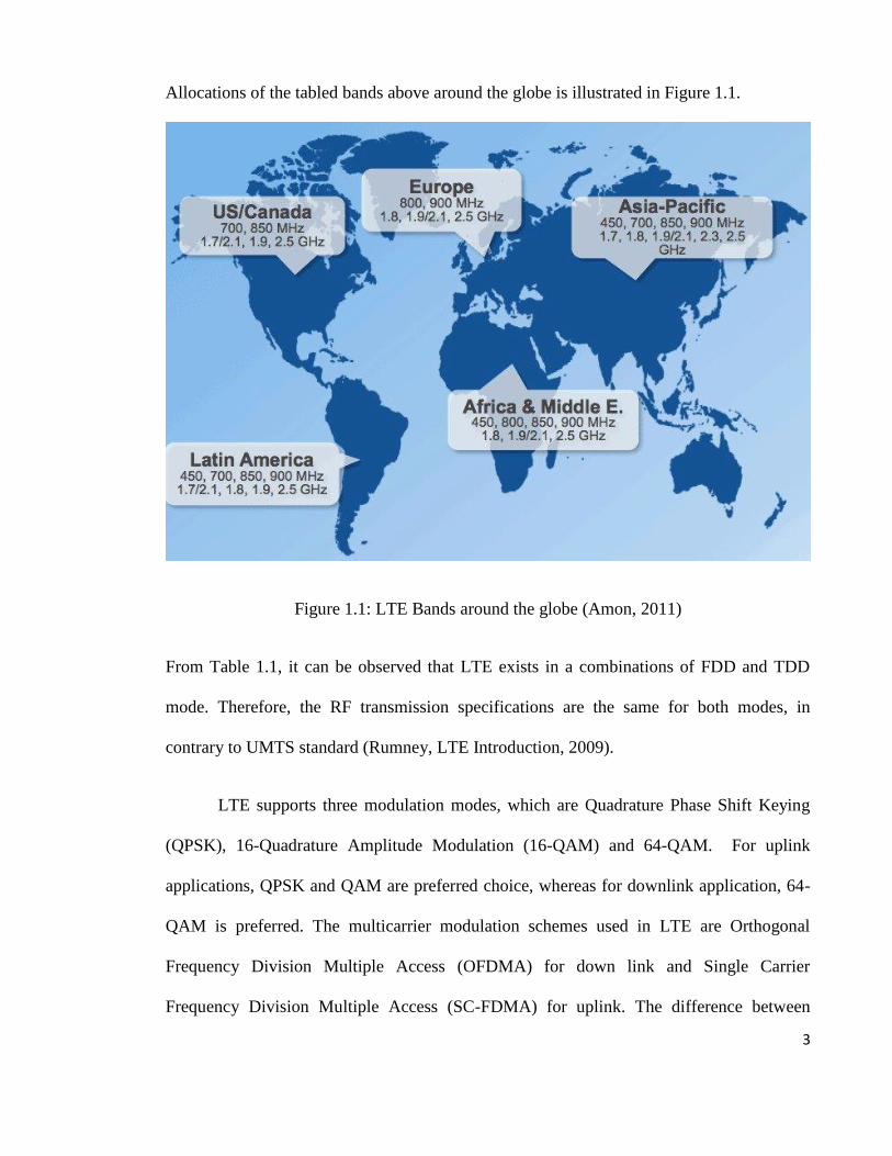
Allocations of the tabled bands above around the globe is illustrated in Figure 1.1.
Figure 1.1: LTE Bands around the globe (Amon, 2011)
From Table 1.1, it can be observed that LTE exists in a combinations of FDD and TDD
mode. Therefore, the RF transmission specifications are the same for both modes, in
contrary to UMTS standard (Rumney, LTE Introduction, 2009).
LTE supports three modulation modes, which are Quadrature Phase Shift Keying
(QPSK), 16-Quadrature Amplitude Modulation (16-QAM) and 64-QAM. For uplink
applications, QPSK and QAM are preferred choice, whereas for downlink application, 64-
QAM is preferred. The multicarrier modulation schemes used in LTE are Orthogonal
Frequency Division Multiple Access (OFDMA) for down link and Single Carrier
Frequency Division Multiple Access (SC-FDMA) for uplink. The difference between
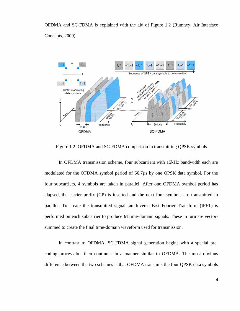
4
OFDMA and SC-FDMA is explained with the aid of Figure 1.2 (Rumney, Air Interface
Concepts, 2009).
Figure 1.2: OFDMA and SC-FDMA comparison in transmitting QPSK symbols
In OFDMA transmission scheme, four subcarriers with 15kHz bandwidth each are
modulated for the OFDMA symbol period of 66.7µs by one QPSK data symbol. For the
four subcarriers, 4 symbols are taken in parallel. After one OFDMA symbol period has
elapsed, the carrier prefix (CP) is inserted and the next four symbols are transmitted in
parallel. To create the transmitted signal, an Inverse Fast Fourier Transform (IFFT) is
performed on each subcarrier to produce M time-domain signals. These in turn are vector-
summed to create the final time-domain waveform used for transmission.
In contrast to OFDMA, SC-FDMA signal generation begins with a special pre-
coding process but then continues in a manner similar to OFDMA. The most obvious
difference between the two schemes is that OFDMA transmits the four QPSK data symbols

5
in parallel, one per subcarrier, while SC-FDMA transmits the four QPSK data symbols in
series at four times the rate, with each data symbol occupying a wider M x 15kHz
bandwidth. This is well illustrated in Figure 1.2. The OFDMA signal clearly behaves as a
multi-carrier with one data symbol per subcarrier, but the SC-FDMA signal appears to be
more like a single-carrier with each data symbol being represented by one wide signal. It is
the parallel transmission of multiple symbols that creates the undesirable high PAPR of
OFDMA. By transmitting the M data symbols in series at M times the rate, the SC-FDMA
occupied bandwidth is the same as multi-carrier OFDMA but, crucially, the PAPR is the
same as that used for the original data symbols. In a nutshell, the PAPR of SC-FDMA is
lower than OFDMA. For example, adding together many narrowband QPSK waveforms in
OFDMA will always create higher peaks than would be seen in the wider bandwidth single
carrier QPSK waveform of SC-FDMA. As the number of subcarriers increases, the PAPR
of OFDMA with random modulating data approaches Gaussian noise statistics but,
regardless the number of sub-carriers, the SC-FDMA PAPR remains the same as that used
for the original data symbols.
1.2 Research Motivation
The setback of SC-FDMA carrier modulation scheme is the generation of non-
constant amplitude signals. Therefore the transmitter circuits particularly power amplifier
(PA) faces stiff challenge in meeting the linear transmission specifications, mainly the
adjacent channel leakage ratio (ACLR) and error vector magnitude (EVM). It’s an uphill
task to meet these specifications without trading off the PA’s efficiency. This is because the
PA needs to operate at certain back-off level from the 1dB compression point in order to
transmit non-constant amplitude signals without clipping them (Raab, et al., 2002).
6
Efficiency is an important figure of merit to protect the battery life of the handset. The first
motivation for this project is to reduce the tradeoff between linearity and efficiency of the
PA so that it is suitable for handset application.
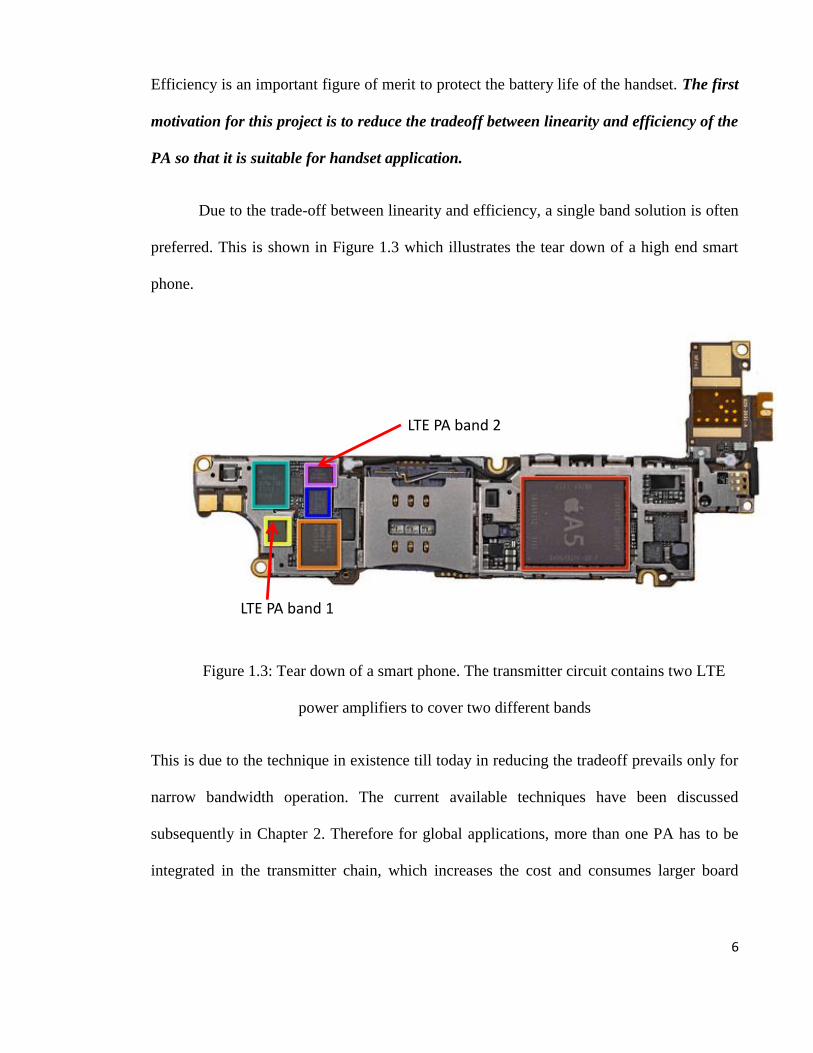
Due to the trade-off between linearity and efficiency, a single band solution is often
preferred. This is shown in Figure 1.3 which illustrates the tear down of a high end smart
phone.
LTE PA band 1
LTE PA band 2
Figure 1.3: Tear down of a smart phone. The transmitter circuit contains two LTE
power amplifiers to cover two different bands
This is due to the technique in existence till today in reducing the tradeoff prevails only for
narrow bandwidth operation. The current available techniques have been discussed
subsequently in Chapter 2. Therefore for global applications, more than one PA has to be
integrated in the transmitter chain, which increases the cost and consumes larger board

7
space. Therefore, the second motivation is to design a multiband LTE PA, where several
bands are integrated in single chip solution.
The third research motivation is to design a high gain PA. This shall serve as an
advantage to the baseband chip which is not designed to deliver high output power. A high
gain PA also shall counter the antenna path loss on the phone board.
The fourth research motivation is to reduce the size of the active chip area of the
PA, which helps in reducing the die manufacturing cost.
1.3 Research Objectives
In this project, the design of a monolithic microwave integrated circuit (MMIC)
power amplifier (PA) for handset was intended. The first research objective was to reduce
the trade-off between linearity and efficiency of the PA. In order to meet this requirement,
the optimum conduction angle technique was used. A conduction angle which has the
lowest third order inter-modulation product (IMD3) and optimum efficiency is chosen to
bias the PA.
The second objective of this research is to improve the efficiency of the PA while
meeting its linearity specifications. The class-J concept was explored to achieve this
objective. The reactive harmonic termination concept is proposed to improve the efficiency
of the PA instead of conventional practice of terminating the second harmonic.
The third objective of this research is to improve the linear operation bandwidth of
the PA. A novel analog pre-distorter (APD) was integrated at the input of the main
amplifier of the PA. The designed APD introduces IMD3 cancellation to improve the
8
adjacent channel leakage ratio (ACLR) which is crucial for linearity. The APD is integrated
on the same chip as the PA.
The fourth objective is to increase the power gain of the PA. A pre-driver and driver
amplifier is integrated in the chip to achieve this objective. This eliminates the need of
external driver amplifier to counter the antenna path loss.
Finally, the fifth objective is to characterize the proposed topology with LTE signal.
This test is essential to ensure PA meets the ACLR and Error Vector Magnitude (EVM)
specifications, thus complying with the 3GPP specifications. Essential optimization was
conducted to meet the stringent linearity requirement for several operating band to fulfill
the multi-band operation objective.
1.4 Thesis Organization
The outline of this thesis is organized as follows. Chapter 2 summarizes the
literature review on various published linearization and efficiency enhancement techniques.
In Chapter 3, the design approach on the power cell, which is the main amplifier is
described and analyzed. Mathematical analysis and lab experiments on choosing the
optimum bias point for linearity and efficiency has also been presented. Chapter 4 presents
the design methodology of the high efficiency wideband class-J PA. The design and
implementation of the Analog Pre-distorter technique is described in Chapter 5.
Subsequently, in Chapter 6 the mode of implementation and measurement results are
presented. Finally, conclusion and suggestion for future works are given in Chapter 7.
9
CHAPTER 2. LITERATURE REVIEW OF POWER AMPLIFIER EFFICIENCY
AND LINEARIZATION TECHNIQUES
2.1 Introduction
LTE employs single carrier frequency division multiple access (SC-FDMA) for
uplink and orthogonal frequency division multiple access (OFDMA) for downlink, a
multicarrier modulation scheme ensuring spectral efficiency (Rana, Islam, & Kouzani,
2010). This modulation scheme is subjected to high peak to average ratio (PAPR). SC-
FDMA has a similar performance and complexity respective to OFDMA, in favor of lower
PAPR (Akter, Islam, & Song, 2010). Typically, the PAPR of SC-FDMA signal is 7dB
whereas OFDMA is 10dB, heavily depending on the modulation scheme adapted (QPSK,
16QAM or 64QAM) (Rumney, Air Interface Concepts, 2009). To amplify signals with high
PAPR, the power amplifier (PA) needs to operate at a backed off output power satisfying
the stringent linearity requirement, specified in terms of adjacent channel leakage ratio
(ACLR) and error vector magnitude (EVM). The drawback of this conventional technique
is in the degradation in PA’s power added efficiency (PAE). The relationship between
backed off output power and efficiency for a multicarrier signal can be appreciated in the
following equations (Cripps, Amplifier Classes, A to S, 2012):
max
1
2
bopbo classA
P
P (2.1)
max4
bopbo classB
P
P
(2.2)
10
where Pbo and Pmax represent backed off output power and maximum output power
respectively. For example, if a PA which has Pmax of 35dBm is transmitting LTE signal
with PAPR of 7dB, the resultant efficiency at Pbo of 28dBm is only 9.9% and 30% in a
respective operation of class A and class B mode.
The solution to improve the PAE of LTE PA lies in two techniques, which are the
efficiency enhancement technique and linearization technique. The efficiency enhancement
technique mandates in improving the efficiency of a linear PA, while linearization
techniques improves the linearity of an efficient non-linear PA (Cripps, RF Power
Amplifiers for Wireless Communications, 2006).
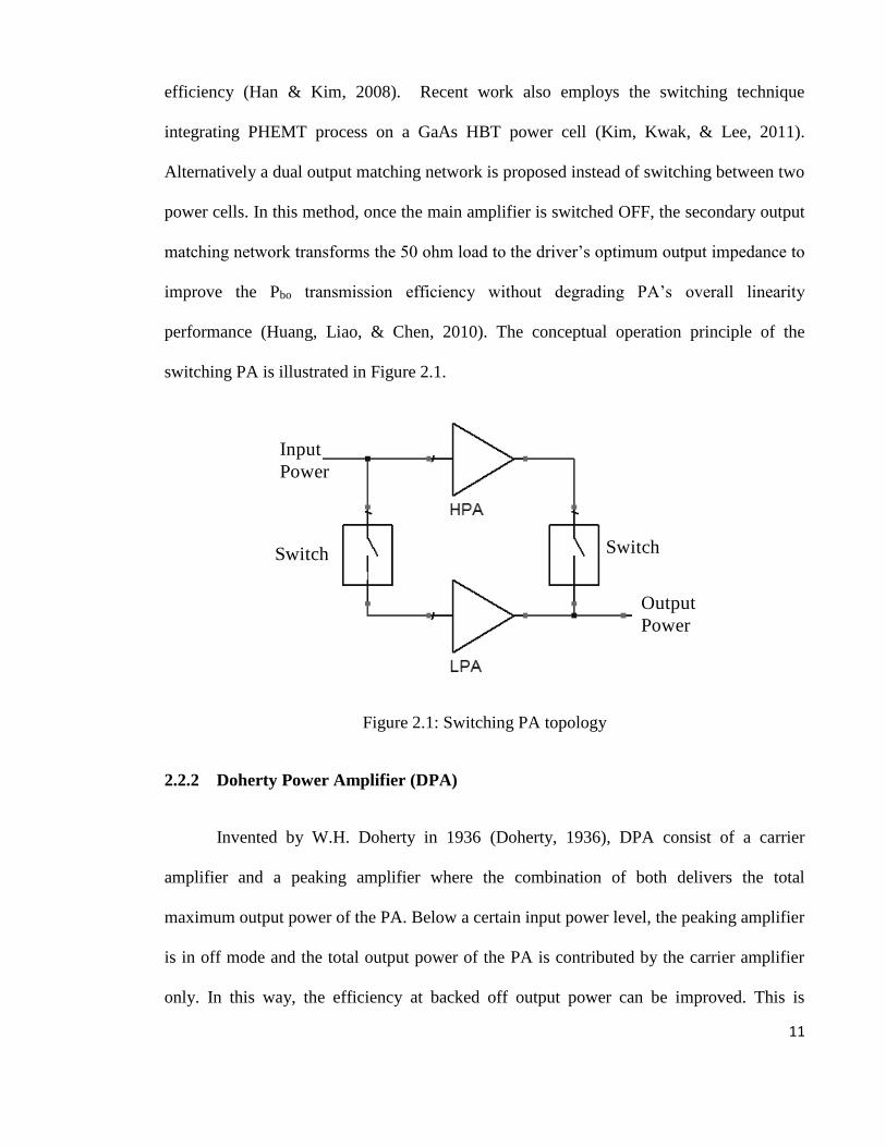
2.2 Efficiency Enhancement Techniques
2.2.1 Device Switching (DS)
Efficiency enhancement technique mandates in improving the efficiency of a linear
PA, which is typically biased at class-AB mode of operation. The device switching
approach is a simple methodology to improve the efficiency of WCDMA PA at Pbo. In this
technique, the size of the power cells is varied respective to the output power. In other
words, the power cells are smaller at Pbo as compared to Pmax, resulting in a higher
efficiency at backed off output power operation region. The switching of the power cells is
executed at the base of the power cells (Deng, Gudem, Larson, Kimball, & Asbeck, A SiGe
PA with Dual Dynamic Bias Control and Memoryless Digital Predistortion for WCDMA
Handset Applications, 2006; Deng, Gudem, Larson, & Asbeck, A High Average Efficiency
SiGe HBT Power Amplifier for WCDMA Handset Applications, 2005). A novel switching
method is reported which utilizes the base-collector diode to improve the switching
11
efficiency (Han & Kim, 2008). Recent work also employs the switching technique
integrating PHEMT process on a GaAs HBT power cell (Kim, Kwak, & Lee, 2011).
Alternatively a dual output matching network is proposed instead of switching between two
power cells. In this method, once the main amplifier is switched OFF, the secondary output
matching network transforms the 50 ohm load to the driver’s optimum output impedance to
improve the Pbo transmission efficiency without degrading PA’s overall linearity
performance (Huang, Liao, & Chen, 2010). The conceptual operation principle of the
switching PA is illustrated in Figure 2.1.
SwitchSwitch
Input
Power
Output
Power
Figure 2.1: Switching PA topology
2.2.2 Doherty Power Amplifier (DPA)
Invented by W.H. Doherty in 1936 (Doherty, 1936), DPA consist of a carrier
amplifier and a peaking amplifier where the combination of both delivers the total
maximum output power of the PA. Below a certain input power level, the peaking amplifier
is in off mode and the total output power of the PA is contributed by the carrier amplifier
only. In this way, the efficiency at backed off output power can be improved. This is
12
usually achieved by varying the load impedance of the single carrier amplifier by applying
another current source at its output terminal. In other words an active load pull is done at
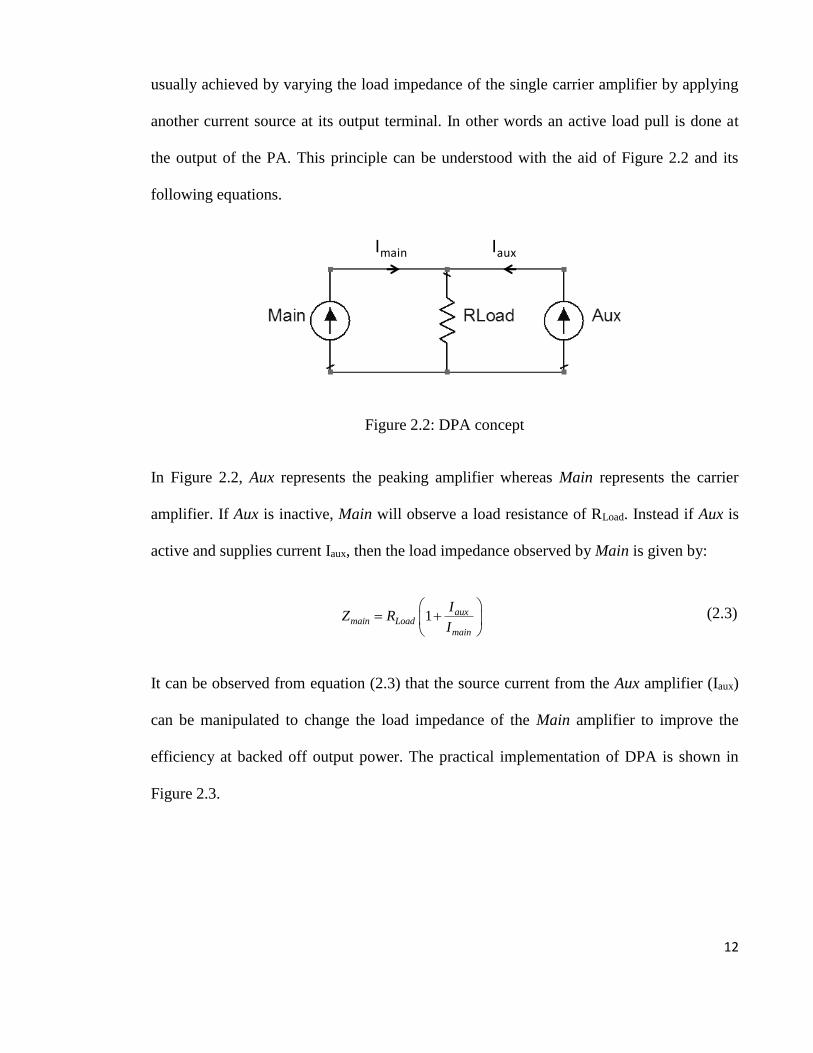
the output of the PA. This principle can be understood with the aid of Figure 2.2 and its
following equations.
Imain Iaux
Figure 2.2: DPA concept
In Figure 2.2, Aux represents the peaking amplifier whereas Main represents the carrier
amplifier. If Aux is inactive, Main will observe a load resistance of RLoad. Instead if Aux is
active and supplies current Iaux, then the load impedance observed by Main is given by:
1 auxmain Load
main
IZ R
I
(2.3)
It can be observed from equation (2.3) that the source current from the Aux amplifier (Iaux)
can be manipulated to change the load impedance of the Main amplifier to improve the
efficiency at backed off output power. The practical implementation of DPA is shown in
Figure 2.3.
13
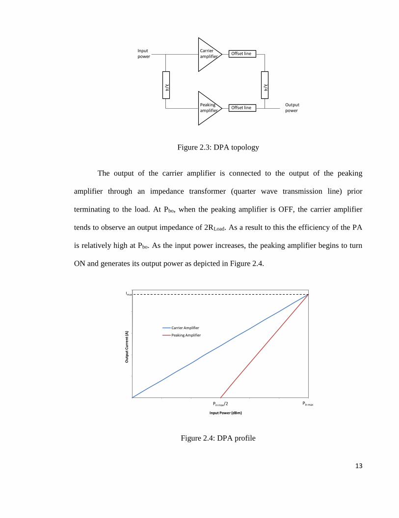
Carrieramplifier
Peakingamplifier
λ/4
λ/4
Inputpower
Outputpower
Offset line
Offset line
Figure 2.3: DPA topology
The output of the carrier amplifier is connected to the output of the peaking
amplifier through an impedance transformer (quarter wave transmission line) prior
terminating to the load. At Pbo, when the peaking amplifier is OFF, the carrier amplifier
tends to observe an output impedance of 2RLoad. As a result to this the efficiency of the PA
is relatively high at Pbo. As the input power increases, the peaking amplifier begins to turn
ON and generates its output power as depicted in Figure 2.4.
Ou
tpu
t C
urr
en
t (A
)
Input Power (dBm)
Carrier Amplifier
Peaking Amplifier
Imax
Pin maxPin max/2
Figure 2.4: DPA profile

14
Accordingly, the load impedance of the carrier amplifier reduces. At Pmax, the load
impedance seen by both amplifiers is RLoad, which generates an equal output power of
Pmax/2 between the carrier and peaking amplifier.
Initial work on DPA in mobile wireless communications highlights a discrete
solution, where the output network responsible for load modulation is integrated on printed
circuit board (Iwamoto, et al., 2001), eventually evolving into a fully integrated approach
(Kato, Yamaguchi, & Kuriyama, 2006). The concept of fully integrated chip using the HBT
technology is extended up to 5 GHz operation (Yu, Kim, Han, Shin, & Kim, 2006).
An on-chip bias control circuit has also been introduced to reduce the tradeoff
between linearity and efficiency at Pbo (Nam & Kim, 2007). Through the introduction of a
third order harmonic control circuitry at the conventional DPA, further improvement in
efficiency is achieved at Pbo (Kang, et al., 2008). Another proposed method is through
optimizing the load modulation by designing an integrated optimum input power divider
(Kang, et al., 2009). Recent work has also proposed wideband architecture for LTE
application (Kang, et al., 2011), where the bandwidth is achieved through the aid of a phase
compensation circuit, which ensures the load modulation is performed successfully across a
wide range of frequency. In another work, switch load power mode technique has been
designed to improve the DPA’s backed off efficiency with the aid of an HEMT amplifier
((Cho, et al., 2014).
2.2.3 Average Bias Tracking (ABT)
The average bias tracking is another popular technique to improve the efficiency of
the PA at Pbo. In this method, the biasing of the PA is adjusted respective to the output
15
power level. Instead of switching between two power devices, both supply voltage and bias
current are dynamically adjusted for a single power cell. At Pbo, the supply voltage and bias
current is low, thus improving the efficiency in this region of operation. The bias controller
circuit is usually implemented on a CMOS platform. The penalty paid is in the inherit
complexity as dual process is needed for the PA realization (Sahu & Rincon-Mora, 2007;
Tombak, Baeten, Jorgenson, & Dening, 2006). There has been a continuous attempt to use
an all CMOS process to reduce the design cost (Shameli, Safarian, Rofougaran,
Rofougaran, & DeFlaviis, 2008). However the PAE and output power is still low as
compared to GaAs based PAs.
2.2.4 Envelope Tracking (ET)
The envelope tracking method was given an immediate attention in the quest to
design an efficient LTE PA. The construction is an evolution from the envelope elimination
and restoration (EER) technique proposed by Kahn (Kahn, 1952). In EER, the phase
modulation of the input signal is preserved, thus eliminating AM-PM distortion. Instead,
the amplitude modulation of the input signal is used to modulate the supply voltage of the
PA to improve the efficiency at Pbo. The improvement is obtained due to the reduction of
the supply voltage in the PA accordingly. For EDGE application, this method is used to
improve the power efficiency of a class-E PA at Pbo (Reynaert & Steyaert, 2005). On the
other hand, the improvement in the bandwidth of the modulator without significantly
degrading its efficiency is also proposed (Chu, Bakkaloglu, & Kiaei, 2008). In EER, the
detection of the amplitude modulated supply voltage at the output of the PA needs to be
accurate to ensure the linearity of the PA (in term of AM-PM distortion) is not jeopardized.
This issue can be resolved by replacing the non-linear PA (class-E, Class-D) with an
16
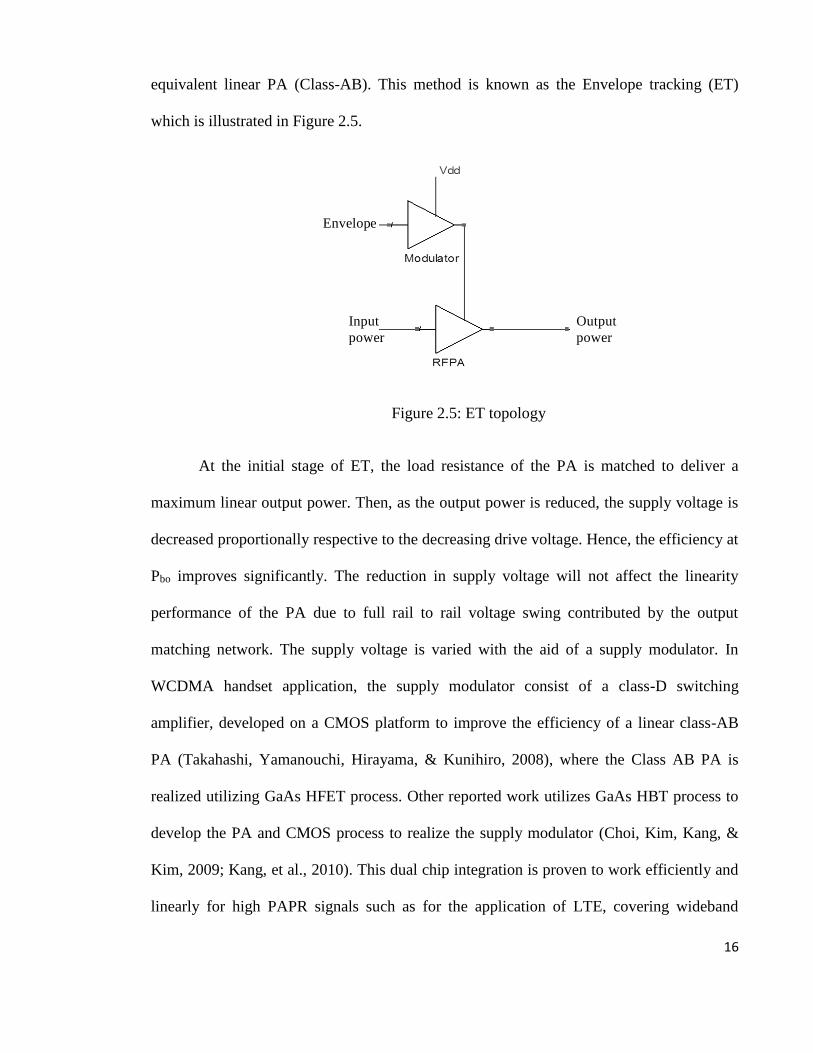
equivalent linear PA (Class-AB). This method is known as the Envelope tracking (ET)
which is illustrated in Figure 2.5.
Envelope
Input
power
Output
power
Figure 2.5: ET topology
At the initial stage of ET, the load resistance of the PA is matched to deliver a
maximum linear output power. Then, as the output power is reduced, the supply voltage is
decreased proportionally respective to the decreasing drive voltage. Hence, the efficiency at
Pbo improves significantly. The reduction in supply voltage will not affect the linearity
performance of the PA due to full rail to rail voltage swing contributed by the output
matching network. The supply voltage is varied with the aid of a supply modulator. In
WCDMA handset application, the supply modulator consist of a class-D switching
amplifier, developed on a CMOS platform to improve the efficiency of a linear class-AB
PA (Takahashi, Yamanouchi, Hirayama, & Kunihiro, 2008), where the Class AB PA is
realized utilizing GaAs HFET process. Other reported work utilizes GaAs HBT process to
develop the PA and CMOS process to realize the supply modulator (Choi, Kim, Kang, &
Kim, 2009; Kang, et al., 2010). This dual chip integration is proven to work efficiently and
linearly for high PAPR signals such as for the application of LTE, covering wideband

17
operation (Moon, Son, Lee, & Kim, 2011; Hassan, Larson, Leung, Kimball, & Asbeck,
2012). In the continuous effort to reduce the complexity and cost, RFPA and supply
modulator is integrated as a single chip solution. For high power application, LDMOS is
used to deliver an efficiency of up to 60% at backed off output power of 31dBm (Pinon,
Hasbani, Giry, Pache, & Garnier, 2008). SiGe BiCMOS process is also well explored in the
PA implementation (Li, Lopez, Wu, Wu, & Lie, 2011; Wang, Kimball, Lie, & Asbeck,
2007). The advantage of low voltage headroom operation in this technology adapts well
into handset transmitter integration frame. However, the GaAs HBT based PA out shines
the SiGe BiCMOS based PA in the linear output power performance. On the other hand, in
the effort to reduce the sensitivity of the supply modulator to battery headroom variation,
new integrated power management architecture is proposed (Choi, Kim, Kang, & Kim, A
New Power Management IC Architecture for Envelope Tracking Power Amplifier, 2011).
An alternative method, known as the interlock operation is also proposed to
enhance the efficiency of the ET PA. Through this method the output current waveform and
the RF input signal is optimized to increase the efficiency of the PA. Optimization of the
RF input signal is executed by increasing the amplitude of the modulated signal at low
output power prior injecting it into the input of the PA, resulting the PA to operate in its
saturated region at low output power, which in turn improves its efficiency (Kim, Son, Jee,
Kim, & Kim, 2013). Recent research work reports on the utilization of the switching
technique to further boost the efficiency of ET PA at Pbo. As an alternative for conventional
series switching techniques, which places series switch at the input and output of the main
amplifier, in current approach a shunt switched capacitor is used to toggle between the low
18
power and high power mode. This technique does not limit the bandwidth of operation in
the PA, thus enables the PA to operate for multiband operation (Cho, et al., 2013).
2.2.5 Class-S
The class-S amplifier is gaining its popularity as a complementing efficient
enhancement technique. Originally meant for audio applications, an improved efficiency
can be achieved for modern RF applications with the aid of GaN process, which promises
high breakdown voltage and fast switching (Rui, Zhancang, Yang, & Lanfranco, 2012;
Maier, et al., 2011; Heinrich, Wentzel, & Melaini, 2010; Wentzel, Meliani, & Heinrich,
2010). Therefore it is a suitable application for high voltage transmitter circuits at current
use.
2.3 Linearization Techniques
2.3.1 Hybrid Class PA
In conventional practice the class-AB PA is the preferred choice in obtaining a good
efficiency performance abstaining the tradeoff on linearity. However for signal with high
PAPR, class-AB is not an optimal solution. Hence, the solution matures into a hybrid
integration of class AB and class-F PA in single chip realization (Kang, et al., A Highly
Efficient and Linear Class-AB/F Power Amplifier for Multimode Operation, 2008). This
solution is achieved by ensuring the fundamental load of the amplifier is sandwiched in
between class F and class-AB loads highlighting an optimum load resistance for linearity
and efficiency. However, the optimum load resistance is obtained only for a narrowband
operation.
19
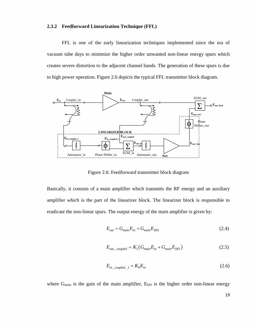
2.3.2 Feedforward Linearization Technique (FFL)
FFL is one of the early linearization techniques implemented since the era of
vacuum tube days to minimize the higher order unwanted non-linear energy spurs which
creates severe distortion to the adjacent channel bands. The generation of these spurs is due
to high power operation. Figure 2.6 depicts the typical FFL transmitter block diagram.
f
S
Sf
Ein Coupler_in
Main
LINEARIZER BLOCK
Eout Coupler_outSUM_out
Eout_final
Eout_corr
Phase
Shifter_out
Eout_Aux
AuxAttenuator_out
Eout_R
Ein_coupled_2
SUM_inPhase Shifter_inAttenuator_in
Ein_coupled_1
Eout_coupled
Figure 2.6: Feedforward transmitter block diagram
Basically, it consists of a main amplifier which transmits the RF energy and an auxiliary
amplifier which is the part of the linearizer block. The linearizer block is responsible to
eradicate the non-linear spurs. The output energy of the main amplifier is given by:
out main in main HOE G E G E (2.4)
_ 1out coupled main in main HOE K G E G E (2.5)
_ _1 0in coupled inE K E (2.6)
where Gmain is the gain of the main amplifier, EHO is the higher order non-linear energy

20
spurs while K0 and K1 is the coupling coefficient of the input and output coupler,
respectively. The amplitude and phase of the coupled undistorted input signal (no higher
order energy) will be attenuated and reversed such that:
_ _ 2 _ 1in coupled out coupled in inE E A K E (2.7)
where Ain is the input attenuation to cancel Gmain.
Therefore, the resultant energy at the output of SUM_in is:
HOmaincoupledincoupledoutRout EGKEEE 12____ (2.8)
The auxiliary amplifier will amplify Eout_R to generate Eout_Aux. With an aid of a phase
shifter, the correction signal is produced, given as:
HOauxcorrout EKGE 1_ (2.9)
where Gaux is the auxiliary amplifier’s gain. With the aid of Attenuator_out and
phase_shifter_out, the Eout_corr can be adjusted to generate an equal EHO amplitude but with
opposite phase response to achieve a perfect cancellation. Finally, the higher order energy
free output signal is given as:
corroutoutfinalout EEE __ (2.10)
The main design challenge in realizing FFL is the generation of the correction
signal Eout_corr. In order to ensure perfect distortion cancellation, a good accuracy in
coupling at the output of the PA and subsequently generate the correction signal is required
in any transmission condition. A possible solution for the above mentioned constraint is to
21
use an adaptive control system to control the amplitude and phase response of the
correction signal. This adaptive control system is realized with the aid of a digital controller
(Suzuki, Ohkawara, & Narahashi, 2011; Legarda, et al., 2005; Kang, Park, Lee, & Hong,
2003). The controller is responsible to generate the amplitude and phase algorithm at
various operating frequencies, to ensure broadband distortion cancellation is achieved.
The usage of coupler in this technique also causes some losses in the fundamental
energy transmission. In order to minimize this losses, the feedforward technique is used as
a pre-distorter where it is connected to the input of the main amplifier, rather than creating
the conventional loop of operation (Kim, et al., 2006).
Due to the complexity of implementation and large board space consumption, the
FFL approach is deemed more suitable for base station applications. Eventually, to improve
on these drawbacks, pre-distortion technique is ventured upon.
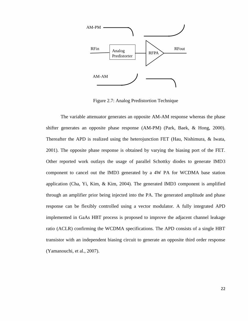
2.3.3 Analog Pre-distortion Linearization (APD)
APD integration is the limelight of PA design due to its simplicity and capability to
be integrated in single chip solution. The principle of operation in APD is through the
generation of inverse phase and magnitude response of the third and fifth order nonlinearity
respective to the corresponding output of the amplifier. In PA design, this reversal in phase
and magnitude can be translated to its AM-AM and AM-PM characteristics as depicted in
Figure 2.7. In other words, the coefficients of the generated non linearity from the APD
cancel the intrinsic non linearity of the PA at the same order. Initial approach shows that a
variable attenuator and phase shifter is used to manually compensate the IMD3 product
generates by the non linear PA.
22
Analog
PredistorterRFPA
RFin RFout
AM-PM
AM-AM
Figure 2.7: Analog Predistortion Technique
The variable attenuator generates an opposite AM-AM response whereas the phase
shifter generates an opposite phase response (AM-PM) (Park, Baek, & Hong, 2000).
Thereafter the APD is realized using the heterojunction FET (Hau, Nishimura, & Iwata,
2001). The opposite phase response is obtained by varying the biasing port of the FET.
Other reported work outlays the usage of parallel Schottky diodes to generate IMD3
component to cancel out the IMD3 generated by a 4W PA for WCDMA base station
application (Cha, Yi, Kim, & Kim, 2004). The generated IMD3 component is amplified
through an amplifier prior being injected into the PA. The generated amplitude and phase
response can be flexibly controlled using a vector modulator. A fully integrated APD
implemented in GaAs HBT process is proposed to improve the adjacent channel leakage
ratio (ACLR) confirming the WCDMA specifications. The APD consists of a single HBT
transistor with an independent biasing circuit to generate an opposite third order response
(Yamanouchi, et al., 2007).
23
2.3.4 Digital Pre-distortion Linearization (DPD)
The major disadvantage of APD techniques mentioned above is in its limited
operation range in which the IMD3 and IMD5 cancellation is quite sensitive to the PA’s
output power and works only for narrow bandwidth. To improve on the bandwidth and to
reduce the sensitivity, DPD is proposed. The DPD adaptation enables an accurate synthesis
of the AM-AM and AM-PM coefficients to generate the 3rd order, 5th order and higher
order cancellation. This improves the linearization dynamic range. Therefore, it can be used
to linearize a highly non-linear PA such as the class-D (Landin, Fritzin, Moer, Isaksson, &
Alvanpour, 2012) and Class-E configuration (Chen, Li, Horng, Jau, & Li, 2009). For
extended application of wideband and high power, the DPD is also integrated together with
envelope tracking technique (Jeong, et al., 2009). Another DPD method which uses the
memory less predistorter techniques to reduce the sampling speed is proposed (Hammi,
Kwan, Bensmida, & Morris, 2014). However, at this point of time the complexity of
implementation and the consumption of larger board space serves are among the
disadvantages DPD technique.
2.3.5 Other Linearization Techniques
As an alternative to the pre-distortion technique, other reported works also
contributed in the effort to improve the linearity of the PA. As such is the bias linearizer
circuit for WCDMA PA (Wen & Sun, 2006). The reverse biased diode maintains a constant
base-emitter voltage (Vbe) across input power, thus effectively improves the gain
compression. The added advantage of this solution is in the reduced DC power
consumption.
24
Another linearization method is the linear amplifications with nonlinear components
(LINC). A novel technique is proposed to reduce the power dissipation at output combiner,
which is achieved through a multi-level out-phasing transmitter scheme (Aref, Askar, Nafe,
Tarar, & Negra, 2012).
The techniques mentioned in section 2.2 and 2.3 are compared in term of linear out
power and corresponding efficiency in Table 2.1.
Table 2.1: Performance Comparison of Various Topologies
Ref Concept Process Freq
(GHz)
Linear
Pout
(dBm)
PAE
(%)
(Huang, Liao,
& Chen, 2010) DS GaAs HBT 1.95 28 34
(Kang, et al.,
2011) DPA GaAs HBT 1.6-2.1 27.5 30
(Shameli,
Safarian,
Rofougaran,
Rofougaran, &
DeFlaviis,
2008)
ABT 0.18um
CMOS 0.9 27.8 34
(Hassan,
Larson, Leung,
Kimball, &
Asbeck, 2012)
ET
GaAs HBT
+ 0.15um
CMOS
2.5 29 43
(Eswaran,
Ramiah,
Kanesan, &
Reza, 2013)
APD GaAs HBT 1.95 29 55
(Chen, Li,
Horng, Jau, &
Li, 2009)
DPD GaAs
PHEMT 1.95 22.7 48
25
2.4 Process Evolution in RFPA Design
An extensive amount of work has been published addressing PA design in CMOS
process, leading to a positive transition from GaAs HBT to CMOS. The major mile stone is
set upon when envelope tracking begins to gain its popularity. As highlighted, the current
practice in ET realization is in the adaptation of dual process technology, CMOS and GaAs
HBT platform, in constructing the PA encapsulating the RFPA and supply modulator.
Favorably if the RFPA is realized in CMOS platform, a single chip solution is feasible
resorting into a cost effective integration. The output power is improved through distributed
active transformer in delivering an output power of more than 25dBm (Francois &
Reyneart, 2012; Tuffery, et al., 2011). Alternately the output power could also be improved
through the introduction of closed loop technique consisting of an amplitude and phase
feedback (Kousai, Onikuza, Yamaguchi, Kuriyama, & Nagaoka, 2012), in which the
operating bandwidth is also subjected to improve. On the other hand, a 90nm fully
integrated CMOS power amplifier which improves the linear output power up to 27.3dBm
is achieved through the couple L-Shape transformer design (Yang, Chen, & Chen, 2014).
Referring to the reviewed published works above, it can be concluded that the
proposed solutions for LTE transmission are scattered around, in terms of linearization and
efficiency improvements. Having said that, efforts on merging this two section as a single
solutions has been lauded despite the higher cost, dual chip fabrications and board space
consumption. Therefore, in this work a significant mileage has been taken to design a PA
with both efficiency and linearization enhancement techniques integrated in one chip
encapsulated to a single fabrication process.
26
CHAPTER 3. POWER CELL DESIGN
3.1 Introduction
In order to obtain the maximum output power for a particular device size, the
optimum load line of the device plays an important role. The load-line determines the
details of the transistor’s collector matching network (Sweet, 1990). For LTE, the
maximum linear output power allowed for reliable transmission by the transmitter system is
23dBm (3GPP TS 36.101 version 9.4.0 Release 9, 2010). Hence, the power amplifier (PA)
needs to transmit at least 28dBm of linear output power to compensate the antenna path
loss (Walsh & Johnson, 2009).
3.2 Power Cell Optimum Size
The optimum load resistance for a single HBT unit cell can be calculated with the
following equation (Sweet, Designing Bipolar Transistor Radio Frequency Integrated
Circuits, 2008):
maxI
VVR kcc
opt
(3.1)
where Vcc is the desired operating voltage, Vk is the IV curve knee voltage and Imax is the
maximum current obtained if the device is biased at class-A biasing point. The IV curve of
a single HBT cell with an area of 80um2 is illustrated in Figure 3.1.
27
Vk
Imax
Figure 3.1: IV curves plot of a HBT with an area size of 80um2
In Figure 3.1, it can be observed that the unit cell’s DC IV curves show a negative slope
due to its self-heating effect. Self-heating effect is caused by the increment of the bias point
of a HBT unit cell in the saturation region (Ganesan, 1993). Therefore in order to protect
the unit cell from this effect, in this work the power cells are designed in such a way that it
comply the current density per unit HBT cell parameter. This is done by determining the
unity gain frequency (fT) of the device. Figure 3.2 illustrates the simulation setup to
determine the unity gain frequency (fT) across collector current for the 80um2 unit cell. In
this simulation, the collector current is increased gradually and the corresponding fT of the
device is determined. The resultant plot is depicted in Figure 3.3.
28
Figure 3.2: Simulation setup to determine the unity gain frequency, fT
22
24
26
28
30
32
34
36
38
40
6 8 10 12 14 16 18 20 22 24 26 28 30 32 34 36 38 40 42
f T(G
Hz)
Ic(mA)
Figure 3.3: Unity gain frequency (fT) across collector current Ic of a HBT with an area size
of 80um2

29
It can be observed from Figure 3.3 that the fT degrades when Ic is more than 30.5mA. With
this the safe operating area (SOA) is defined as:
Area
MaxSOA cT I f
(3.2)
280
5.30
um
mA
= 0.38mA/um2
Therefore in this work the maximum current density per unit cell has been set to
0.38mA/um2.
Since the targeted maximum linear output power is 28dBm, therefore the initial
value for the maximum saturated output power of the amplifier is set to 32dBm. In other
words, the back-off level is set to at least 4dB. This is an effort to optimize the efficiency of
the PA with optimal device size. This can be viewed through equation (3.1) where smaller
device will have larger Ropt and smaller Imax for the exact supply voltage headroom. The
methodology to determine the power cell size is as follows:
1) Targeted maximum output power: 32dBm
2) Convert to Watt:
( )
10( ) 10 1
outP dBm
outP W mW
(3.3)
30
32
310( ) 10 1 10outP W
= 1.58W
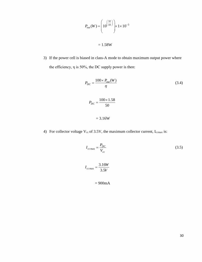
3) If the power cell is biased in class-A mode to obtain maximum output power where
the efficiency, η is 50%, the DC supply power is then:
100 ( )outDC
P WP
(3.4)
100 1.58
50DCP
= 3.16W
4) For collector voltage Vcc of 3.5V, the maximum collector current, Iccmax is:
maxDC
cc
cc
PI
V (3.5)
max
3.16
3.5cc
WI
V
= 900mA

31
5) Referring to Figure 3.1, Icc of 15mA is selected as in this saturation region device is
not severely affected by self-heating. Therefore the number of unit cells required:
maxcc
ccunitcell
IN
I (3.6)
900
15N
N= 60
The number of unit cells required is 60.
6) The total device size is:
size (Q) single unit sizeTotal N (3.7)
Q 60 80
= 4800um2
Therefore the calculated power cell size is 4800um2.
The load resistance of the power cell is calculated as following:
1) Rload of a single unit cell using equation (3.1):
max
cc kopt
V VR
I
3.5 0.5
0.015optR
= 200Ω
32
2) The Rload of the power cell with size of 4800um2 :
opt
load
RR
N (3.8)
200
60loadR
= 3.33Ω
The calculated load resistance of 3.33Ω delivers a maximum output power of 32dBm.
The above calculated power cell size and its corresponding load resistance are verified in
simulation. Figure 3.4 shows the schematic of the power cell. …….
Device 20
Icc1
Icc2
Vc
Vbb
C2
Device 2
Rss2
Rss1C1
RFin
Device 1
Figure 3.4: Power cell of the LTE PA. There are total 20 numbers of cells. Rss is the
ballasting resistor and C1 and C2 are the coupling capacitor
33
The size of each cell in Figure 3.4 is:
Cell size= Emitter width (µm) x Emitter Length (µm) x Number of emitter (3.9)
= 3 x 20 x 4
= 240um2
The cells size is multiplied by 20 to achieve the overall size of 4800um2. The simulation
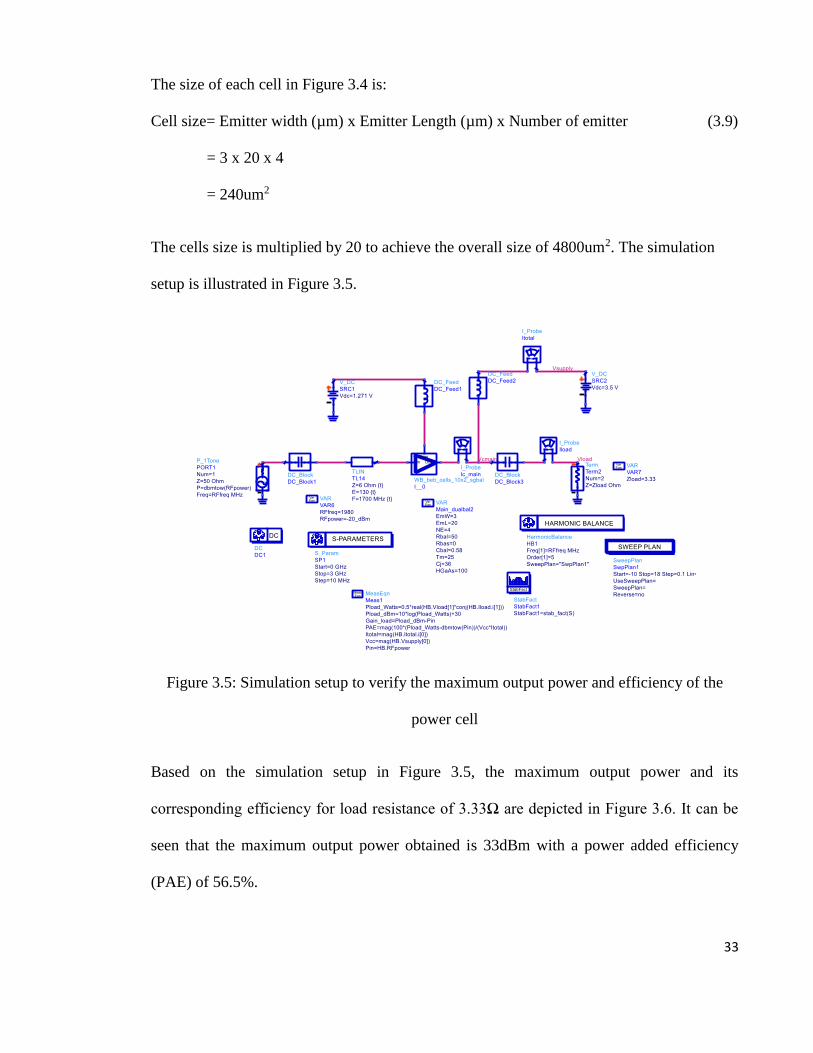
setup is illustrated in Figure 3.5.
Figure 3.5: Simulation setup to verify the maximum output power and efficiency of the
power cell
Based on the simulation setup in Figure 3.5, the maximum output power and its
corresponding efficiency for load resistance of 3.33Ω are depicted in Figure 3.6. It can be
seen that the maximum output power obtained is 33dBm with a power added efficiency
(PAE) of 56.5%.
34
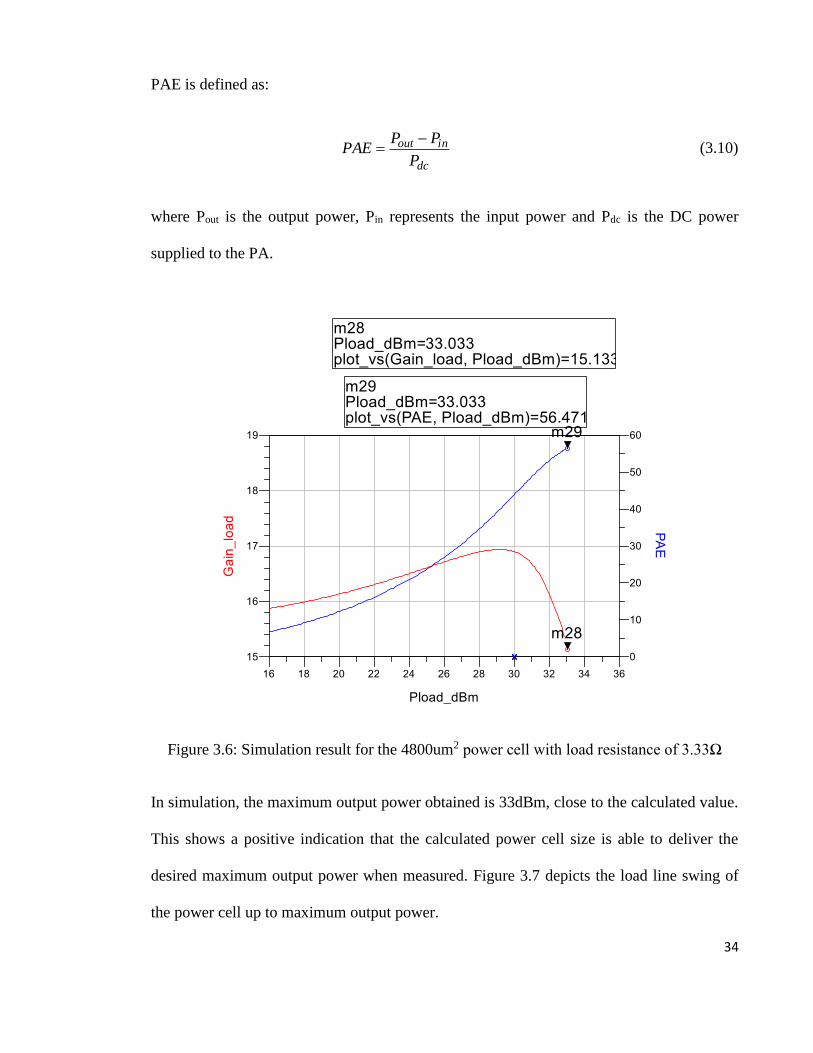
PAE is defined as:
dc
inout
P
PPPAE
(3.10)
where Pout is the output power, Pin represents the input power and Pdc is the DC power
supplied to the PA.
Figure 3.6: Simulation result for the 4800um2 power cell with load resistance of 3.33Ω
In simulation, the maximum output power obtained is 33dBm, close to the calculated value.
This shows a positive indication that the calculated power cell size is able to deliver the
desired maximum output power when measured. Figure 3.7 depicts the load line swing of
the power cell up to maximum output power.
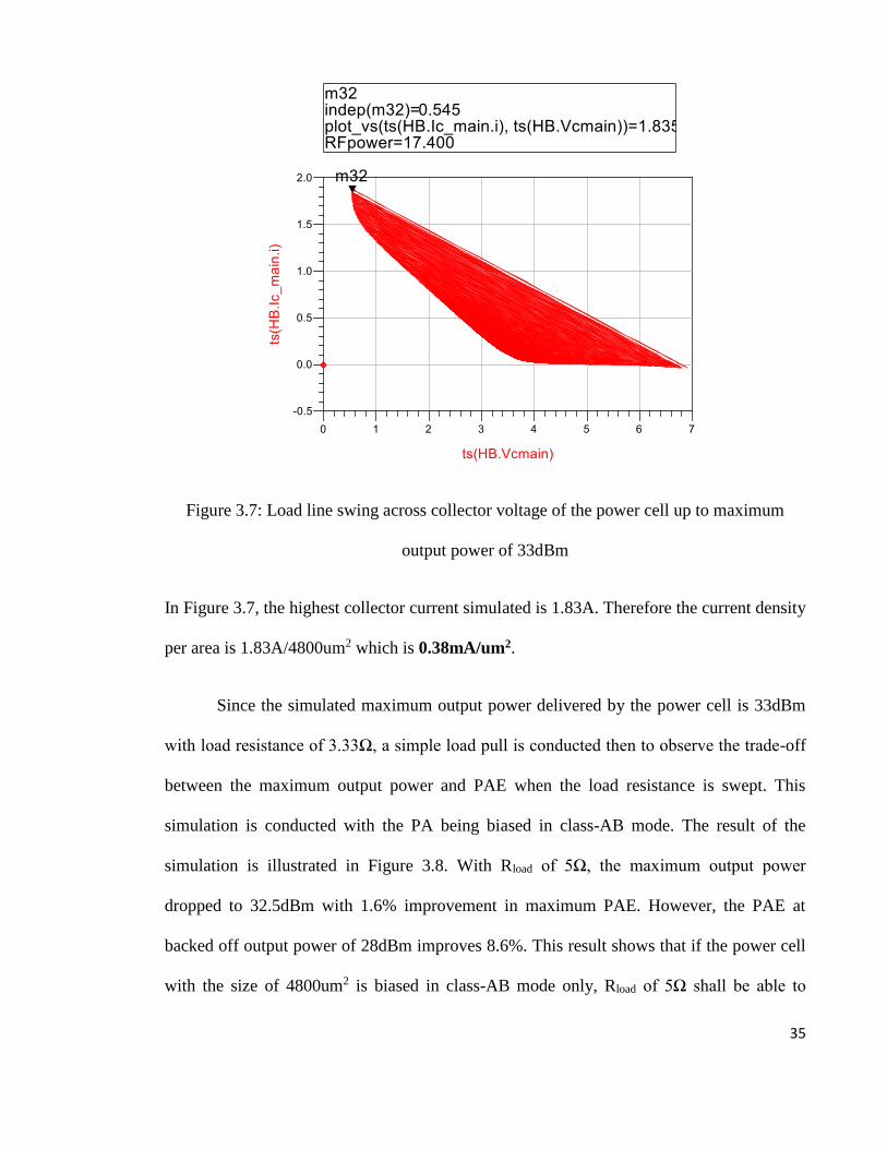
35
Figure 3.7: Load line swing across collector voltage of the power cell up to maximum
output power of 33dBm
In Figure 3.7, the highest collector current simulated is 1.83A. Therefore the current density
per area is 1.83A/4800um2 which is 0.38mA/um2.
Since the simulated maximum output power delivered by the power cell is 33dBm
with load resistance of 3.33Ω, a simple load pull is conducted then to observe the trade-off
between the maximum output power and PAE when the load resistance is swept. This
simulation is conducted with the PA being biased in class-AB mode. The result of the
simulation is illustrated in Figure 3.8. With Rload of 5Ω, the maximum output power
dropped to 32.5dBm with 1.6% improvement in maximum PAE. However, the PAE at
backed off output power of 28dBm improves 8.6%. This result shows that if the power cell
with the size of 4800um2 is biased in class-AB mode only, Rload of 5Ω shall be able to
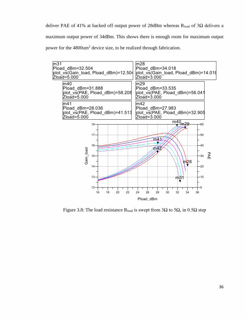
36
deliver PAE of 41% at backed off output power of 28dBm whereas Rload of 3Ω delivers a
maximum output power of 34dBm. This shows there is enough room for maximum output
power for the 4800um2 device size, to be realized through fabrication.
Figure 3.8: The load resistance Rload is swept from 3Ω to 5Ω, in 0.5Ω step
37
3.3 Thermal Runaway Phenomenon
3.3.1 Thermal runaway in HBT
The ability to deliver high output power at high frequency favors Hybrid Bipolar
Transistor (HBT) technology as a solution for high frequency PA design (Sweet, Designing
Bipolar Transistor Radio Frequency Integrated Circuits, 2008). However, due to its positive
temperature coefficient characteristic, HBT is susceptible to an undesired phenomenon,
known as thermal runaway. Liu et.al reported that, this is due to the collapse of current gain
as the temperature of HBT increases (Liu, Nelson, Hill, & Khatibzadeh, 1993). An
analytical model has been accordingly presented in predicting this phenomenon to certain
accuracy (Liou, Liou, & Huang, 1994). The collapse of current gain is initiated, in the event
the current of the parallel multiple HBT unit cells tumble. The parallel configuration is
essential in delivering high transmission output power. Current collapse commences if any
of the unit cell operates at higher temperature due to self-heating effect. The aftermath of
this effect observes a higher collector current being injected by the designated unit cell.
Higher collector current would eventually lead to a dependent chain of increase in the unit
cell temperature. Subsequently the base-emitter voltage of the cell will drop due to the self-
heating effect, resulting in the collector current hogs the remaining active unit cell. Current
hogging increases the temperature and subsequently shuts down the remaining unit cells.
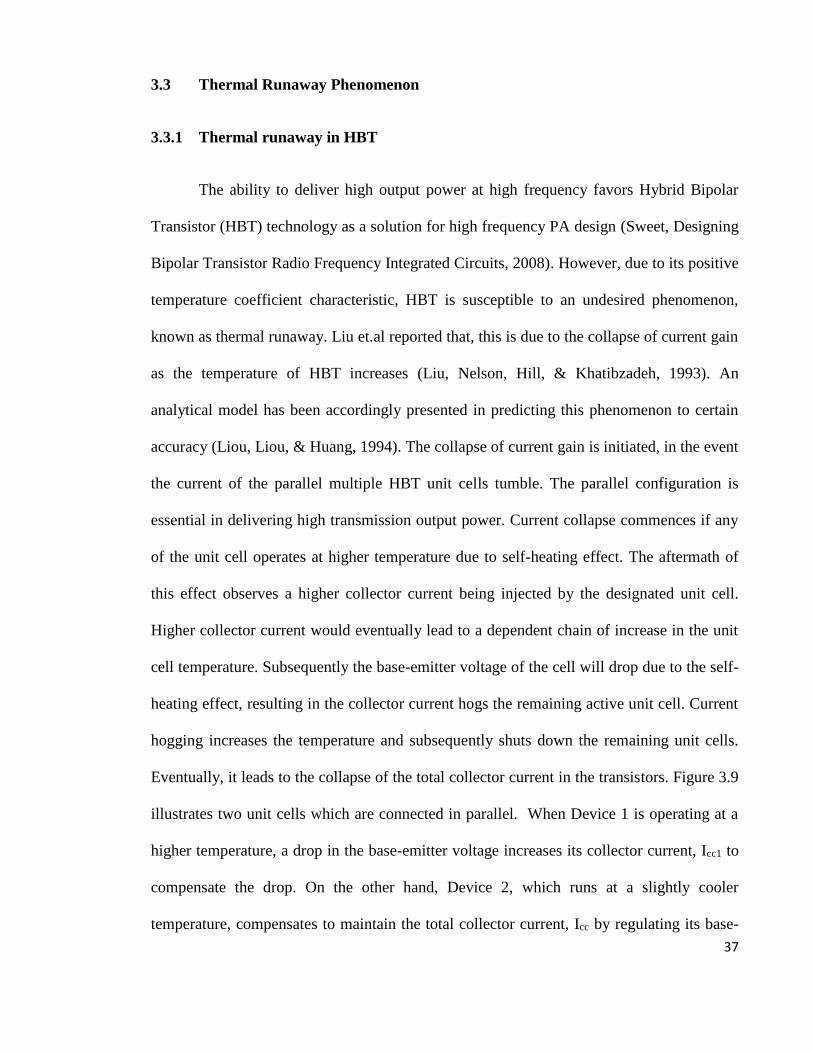
Eventually, it leads to the collapse of the total collector current in the transistors. Figure 3.9
illustrates two unit cells which are connected in parallel. When Device 1 is operating at a
higher temperature, a drop in the base-emitter voltage increases its collector current, Icc1 to
compensate the drop. On the other hand, Device 2, which runs at a slightly cooler
temperature, compensates to maintain the total collector current, Icc by regulating its base-
38
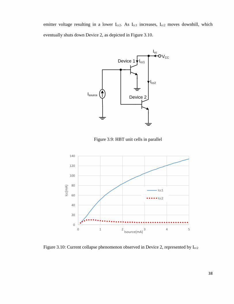
emitter voltage resulting in a lower Icc2. As Icc1 increases, Icc2 moves downhill, which
eventually shuts down Device 2, as depicted in Figure 3.10.
Device 1
IsourceDevice 2
VCC
Icc1
Icc2
Icc
Figure 3.9: HBT unit cells in parallel
0
20
40
60
80
100
120
140
0 1 2 3 4 5
Icc(
mA
)
Isource(mA)
Icc1
Icc2
Figure 3.10: Current collapse phenomenon observed in Device 2, represented by Icc2
39
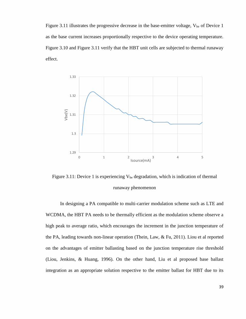
Figure 3.11 illustrates the progressive decrease in the base-emitter voltage, Vbe of Device 1
as the base current increases proportionally respective to the device operating temperature.
Figure 3.10 and Figure 3.11 verify that the HBT unit cells are subjected to thermal runaway
effect.
1.29
1.3
1.31
1.32
1.33
0 1 2 3 4 5
Vb
e(V
)
Isource(mA)
Figure 3.11: Device 1 is experiencing Vbe degradation, which is indication of thermal
runaway phenomenon
In designing a PA compatible to multi-carrier modulation scheme such as LTE and
WCDMA, the HBT PA needs to be thermally efficient as the modulation scheme observe a
high peak to average ratio, which encourages the increment in the junction temperature of
the PA, leading towards non-linear operation (Thein, Law, & Fu, 2011). Liou et al reported
on the advantages of emitter ballasting based on the junction temperature rise threshold
(Liou, Jenkins, & Huang, 1996). On the other hand, Liu et al proposed base ballast
integration as an appropriate solution respective to the emitter ballast for HBT due to its
40
decreasing current gain to temperature dependency (Liu, Khatibzadeh, Sweder, & Chau,
1996). However, base ballast tends to degrade the power gain of the PA and contributes to
the degradation of linear output power (Maas, 2006). Jang et al alternatively integrated a
depletion FET to the base of HBT to act as non-linear base ballast outlining thermal
stability (Jang, Kan, Arnborg, Johansson, & Dutton, 1998), with a penalty paid in the
complexity of the physical layout and fabrication cost. On the other hand, Jin-Dong et al
proposed an optimized value of base ballast resistor based on thermal feedback network
analysis to reduce the trade-off in power gain. Based on computer aided simulation result,
HBT architecture conceptually requires a smaller base ballast resistor as compared to BJT
(Dong, Zhang, Jun, Pan, & Ying, 2006). Bayraktaroglu et al alternatively proposed for a
thermal isolation circuit to be integrated between the current source and the power stage as
a substitute of the base ballasting concept (Bayraktaroglu & Salib, 1997).
3.3.2 Thermal Compensation Circuit
Figure 3.12 describes the circuit diagram of integrating the strap resistors, Rss1 and Rss2.
Expressing the temperature delta of both devices in Figure 3.12 as:
jc dT P
(3.11)
where θjc is the thermal resistance and Pd is the power dissipated, defined to be:
d cc cP I V (3.12)
where Icc = Icc1 + Icc2.
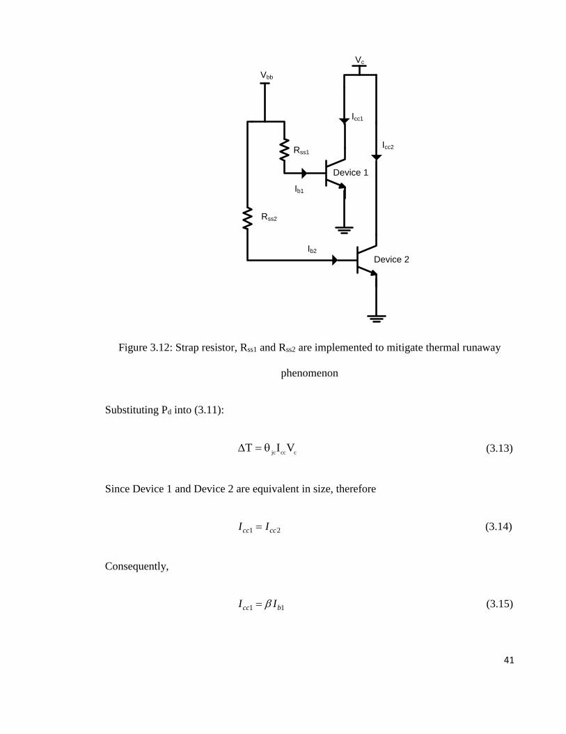
41
Icc1
Icc2
Vc
Vbb
Device 2
Rss2
Rss1
Device 1
Ib2
Ib1
Figure 3.12: Strap resistor, Rss1 and Rss2 are implemented to mitigate thermal runaway
phenomenon
Substituting Pd into (3.11):
jc cc cT I V
(3.13)
Since Device 1 and Device 2 are equivalent in size, therefore
1 2cc ccI I (3.14)
Consequently,
1 1cc bI I (3.15)
42
and
2 2cc bI I (3.16)
The relationship between the base currents and strap resistors is given as:
1
1
bbb
ss
VI
R (3.17)
and
2
2
bbb
ss
VI
R (3.18)
Substituting Ib1 and Ib2 in equation (3.15) and (3.16) respectively:
1
1
bbcc
ss
VI
R (3.19)
and
2
2
bbcc
ss
VI
R (3.20)
The total collector current Icc can be equated as:
1 2
1 2
1 1
=
cc bb
ss ss
bb
ss ss
I VR R
V
R R
(3.21)
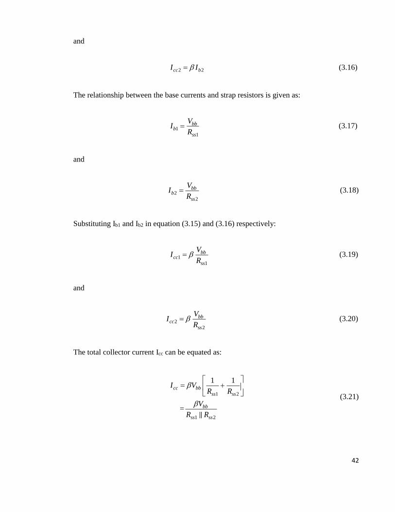
43
substituting (3.21) into (3.13):
bb
jc c
ss1 ss2
VT V
R || R
(3.22)
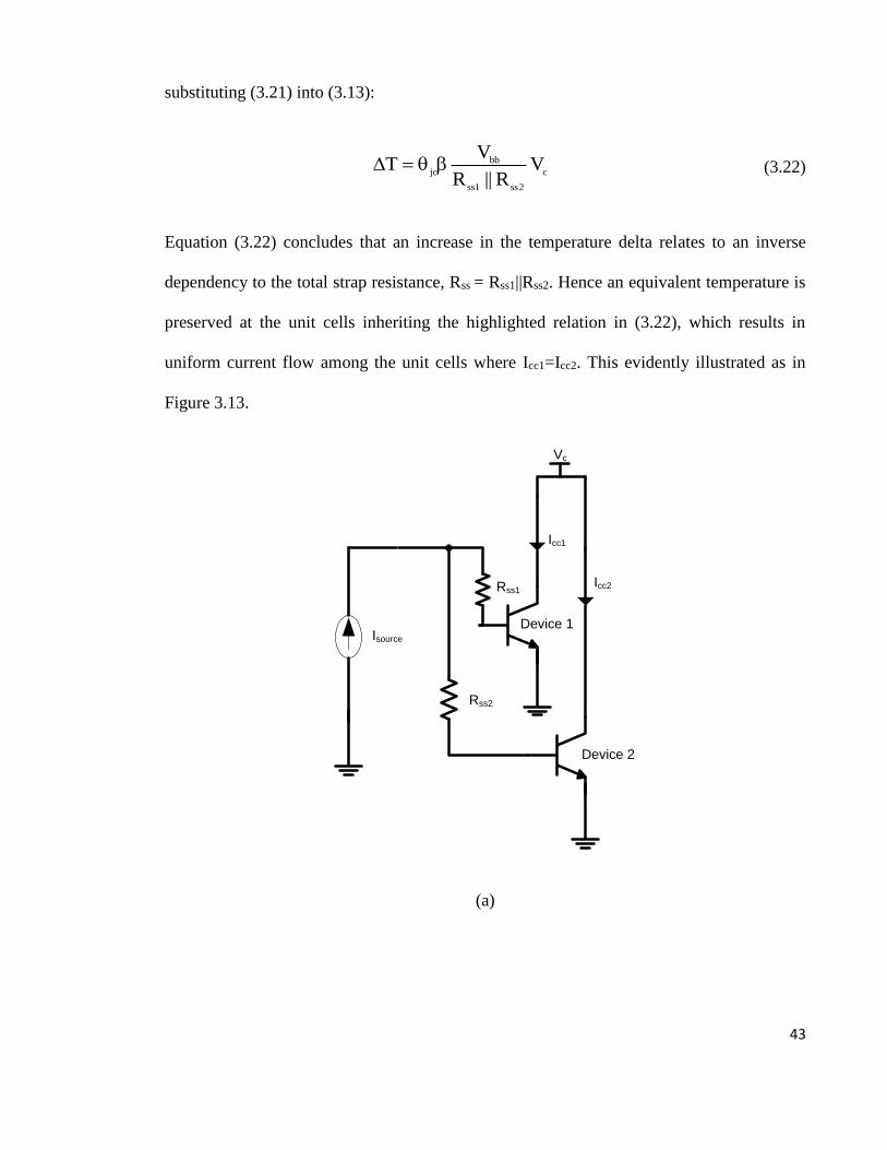
Equation (3.22) concludes that an increase in the temperature delta relates to an inverse
dependency to the total strap resistance, Rss = Rss1||Rss2. Hence an equivalent temperature is
preserved at the unit cells inheriting the highlighted relation in (3.22), which results in
uniform current flow among the unit cells where Icc1=Icc2. This evidently illustrated as in
Figure 3.13.
Icc1
Icc2
Vc
Device 2
Rss2
Rss1
Device 1Isource
(a)
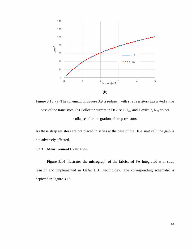
44
0
20
40
60
80
100
120
140
0 1 2 3 4 5
Icc(
mA
)
Isource(mA)
Icc1
Icc2
(b)
Figure 3.13: (a) The schematic in Figure 3.9 is redrawn with strap resistors integrated at the
base of the transistors. (b) Collector current in Device 1, Icc1 and Device 2, Icc2 do not
collapse after integration of strap resistors
As these strap resistors are not placed in series at the base of the HBT unit cell, the gain is
not adversely affected.
3.3.3 Measurement Evaluation
Figure 3.14 illustrates the micrograph of the fabricated PA integrated with strap
resistor and implemented in GaAs HBT technology. The corresponding schematic is
depicted in Figure 3.15.
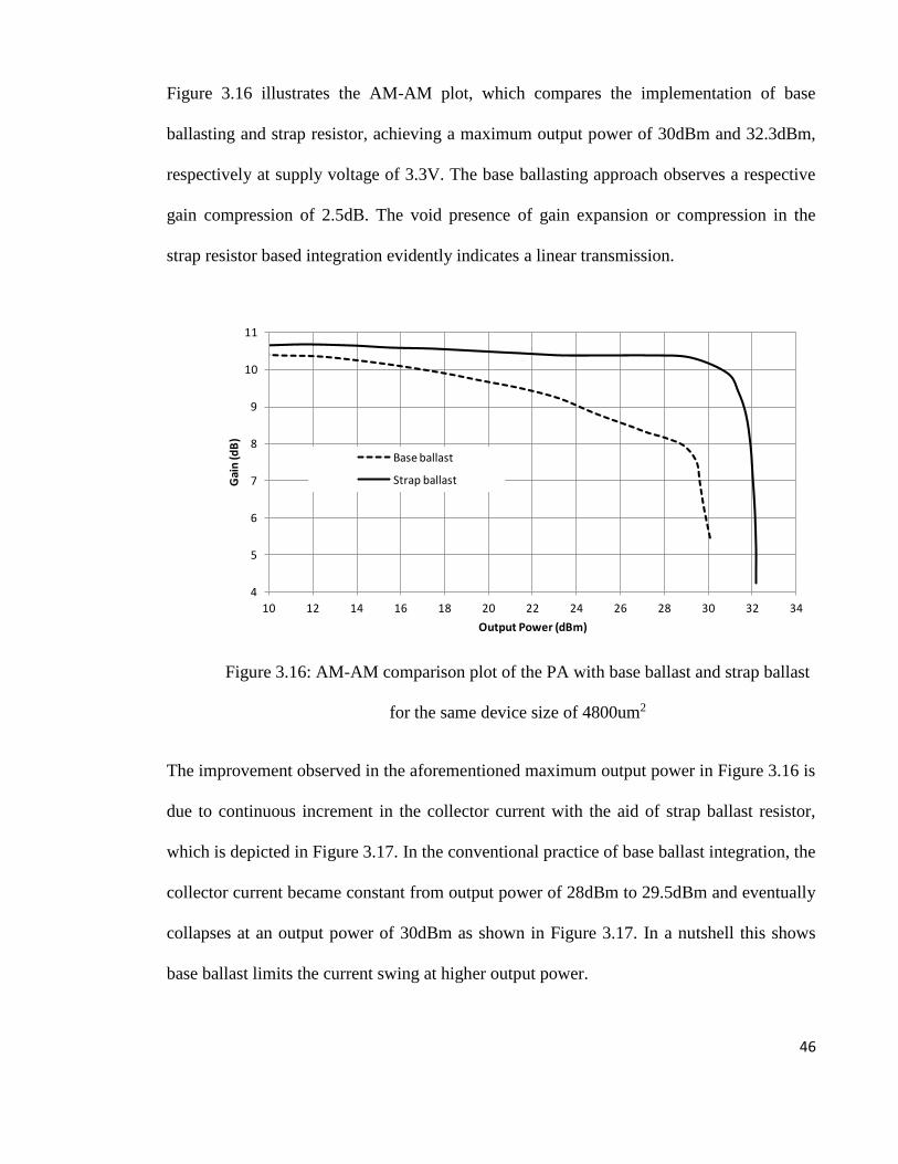
45
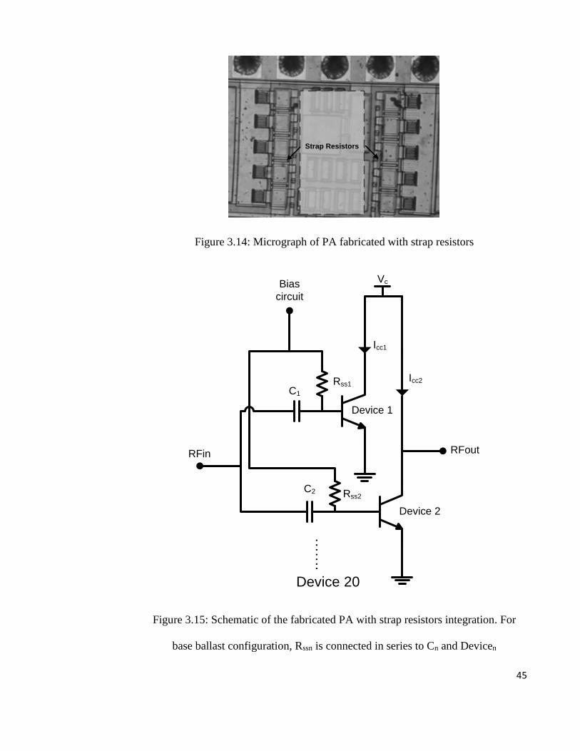
Strap Resistors
Figure 3.14: Micrograph of PA fabricated with strap resistors
Icc1
Icc2
Vc
C2
Device 2
Rss2
Rss1C1
RFin
Device 1
Bias
circuit
RFout
…….
Device 20
Figure 3.15: Schematic of the fabricated PA with strap resistors integration. For
base ballast configuration, Rssn is connected in series to Cn and Devicen
46
Figure 3.16 illustrates the AM-AM plot, which compares the implementation of base
ballasting and strap resistor, achieving a maximum output power of 30dBm and 32.3dBm,
respectively at supply voltage of 3.3V. The base ballasting approach observes a respective
gain compression of 2.5dB. The void presence of gain expansion or compression in the
strap resistor based integration evidently indicates a linear transmission.
4
5
6
7
8
9
10
11
10 12 14 16 18 20 22 24 26 28 30 32 34
Gai
n (d
B)
Output Power (dBm)
Base ballast
Strap ballast
Figure 3.16: AM-AM comparison plot of the PA with base ballast and strap ballast
for the same device size of 4800um2
The improvement observed in the aforementioned maximum output power in Figure 3.16 is
due to continuous increment in the collector current with the aid of strap ballast resistor,
which is depicted in Figure 3.17. In the conventional practice of base ballast integration, the
collector current became constant from output power of 28dBm to 29.5dBm and eventually
collapses at an output power of 30dBm as shown in Figure 3.17. In a nutshell this shows
base ballast limits the current swing at higher output power.
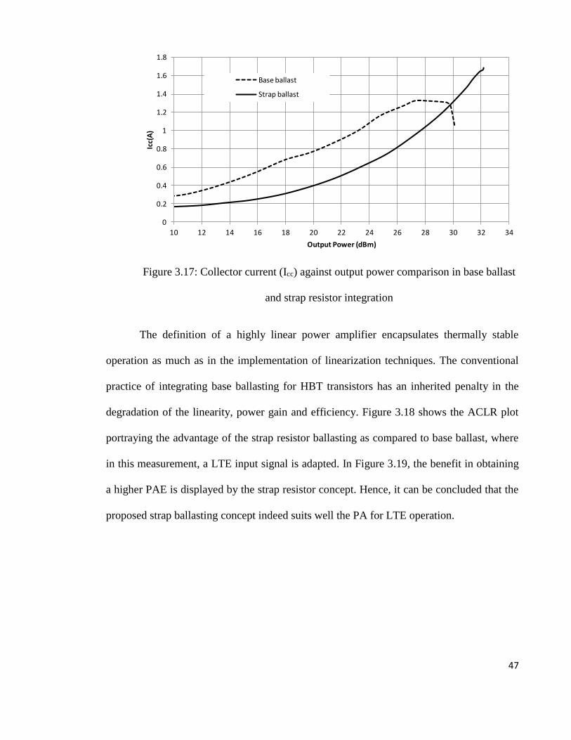
47
0
0.2
0.4
0.6
0.8
1
1.2
1.4
1.6
1.8
10 12 14 16 18 20 22 24 26 28 30 32 34
Icc(
A)
Output Power (dBm)
Base ballast
Strap ballast
Figure 3.17: Collector current (Icc) against output power comparison in base ballast
and strap resistor integration
The definition of a highly linear power amplifier encapsulates thermally stable
operation as much as in the implementation of linearization techniques. The conventional
practice of integrating base ballasting for HBT transistors has an inherited penalty in the
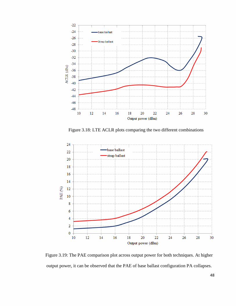
degradation of the linearity, power gain and efficiency. Figure 3.18 shows the ACLR plot
portraying the advantage of the strap resistor ballasting as compared to base ballast, where
in this measurement, a LTE input signal is adapted. In Figure 3.19, the benefit in obtaining
a higher PAE is displayed by the strap resistor concept. Hence, it can be concluded that the
proposed strap ballasting concept indeed suits well the PA for LTE operation.
48
Figure 3.18: LTE ACLR plots comparing the two different combinations
Figure 3.19: The PAE comparison plot across output power for both techniques. At higher
output power, it can be observed that the PAE of base ballast configuration PA collapses.

49
Therefore it can be concluded strap resistors not only prevent the collapse of current at high
input power, but also guarantees a higher linear output power and PAE delivery as
compared to the conventional practice base ballast integration. Therefore, in this work, this
concept is applied in the PA design as an effort to preserve its linear output power and
PAE.
3.4 Power Cell Optimum Conduction Angle
3.4.1 Fourier Analysis
The trade-off between linear operation and efficiency is fundamentally determined
by the PA’s biasing point, alternately known as the conduction angle of the PA. Selecting
an optimum conduction angle is essential in designing a linear and efficient PA. As the
conduction angle reduces, the rise of even and odd orders components are more significant.
Third order component adversely affects the linearity performance of the PA. Cripps has
conducted a mathematical analysis to determine the even and odd order responses for a
FET transistor (Cripps, RF Power Amplifiers for Wireless Communications, 2006).
Adapting the analysis as a reference, a similar mathematical analysis has been done for the
HBT transistor in this work and extended up to 5th order components. Figure 3.20 illustrates
the RF collector current waveform plot of a class B HBT amplifier.
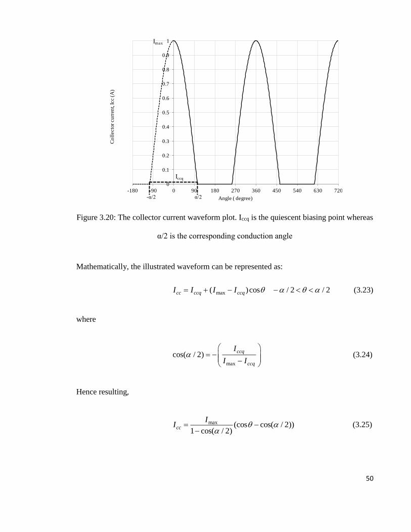
50
0
0.1
0.2
0.3
0.4
0.5
0.6
0.7
0.8
0.9
1
-180 -90 0 90 180 270 360 450 540 630 720
Co
llecto
r cu
rren
t, Icc (
A)
Angle ( degree)
Iccq
α/2
Imax
-α/2
Figure 3.20: The collector current waveform plot. Iccq is the quiescent biasing point whereas
α/2 is the corresponding conduction angle
Mathematically, the illustrated waveform can be represented as:
max( )cos / 2 / 2cc ccq ccqI I I I (3.23)
where
max
cos( / 2)ccq
ccq
I
I I
(3.24)
Hence resulting,
max (cos cos( / 2))1 cos( / 2)
cc
II
(3.25)
51
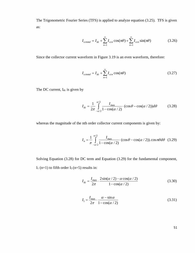
The Trigonometric Fourier Series (TFS) is applied to analyze equation (3.25). TFS is given
as:
1 1
cos( ) sin( )cctotal dc ccn ccn
n n
I I I n I n
(3.26)
Since the collector current waveform in Figure 3.19 is an even waveform, therefore:
1
cos( )cctotal dc ccn
n
I I I n
(3.27)
The DC current, Idc is given by
/2
max
/2
1(cos cos( / 2))
2 1 cos( / 2)dc
II d
(3.28)
whereas the magnitude of the nth order collector current components is given by:
/2
max
/2
1(cos cos( / 2)).cos
1 cos( / 2)n
II n d
(3.29)
Solving Equation (3.28) for DC term and Equation (3.29) for the fundamental component,
I1 (n=1) to fifth order I5 (n=5) results in:
max 2sin( / 2) cos( / 2)
2 1 cos( / 2)dc
II
(3.30)
max1
sin
2 1 cos( / 2)
II
(3.31)
52
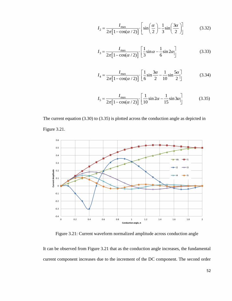
max
2
1 3sin sin
2 1 cos( / 2) 2 3 2
II
(3.32)
max
3
1 1sin sin 2
2 1 cos( / 2) 3 6
II
(3.33)
max
4
1 3 1 5sin sin
2 1 cos( / 2) 6 2 10 2
II
(3.34)
max
5
1 1sin 2 sin3
2 1 cos( / 2) 10 15
II
(3.35)
The current equation (3.30) to (3.35) is plotted across the conduction angle as depicted in
Figure 3.21.
-0.4
-0.3
-0.2
-0.1
0
0.1
0.2
0.3
0.4
0.5
0.6
0 0.2 0.4 0.6 0.8 1 1.2 1.4 1.6 1.8 2
Cu
rre
nt
Am
plit
ud
e
Conduction angle, π
Idc I1
I2 I3
I4 I5
Figure 3.21: Current waveform normalized amplitude across conduction angle
It can be observed from Figure 3.21 that as the conduction angle increases, the fundamental
current component increases due to the increment of the DC component. The second order
53
component which translates to second harmonic has an amplitude more than 0 from 0.5π to
1.5π. The peak is at 0.8π, which is close to class-B biasing. On the other hand, the third
order current component also reduces as the conduction angle increases. An interesting
observation is at the conduction angle within the range of π<α<1.8π. In this region, the
fundamental component is the highest and the third order component is at the lowest. This
shows that it is theoretically possible to obtain higher fundamental output power, although
the PA is not biased at class-A (conduction angle 2π) mode. The lowest third order
component on the other hand promises a linear operation to a certain extent without
sacrificing the efficiency at much.
3.4.2 Relationship between Conduction Angle and Efficiency
In order to determine the efficiency corresponding to α=2π which represents the
conduction angle of a class-A amplifier, Equation (3.30) and (3.31) is appreciated, resulting
in Idc= Imax/2π and I1= Imax/2π hence reflecting the efficiency of class A, which is I1/Idc to be
1. Using this result, the relationship between the conduction angle and efficiency in
reference to class-A mode is given by:
1 .1dc
I
I (3.36)
1 . class A
dc
I
I (3.37)
Subsequently from equation (3.30) and (3.31):
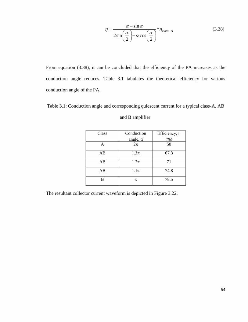
54
sin
*
2sin cos2 2
class A
(3.38)
From equation (3.38), it can be concluded that the efficiency of the PA increases as the
conduction angle reduces. Table 3.1 tabulates the theoretical efficiency for various
conduction angle of the PA.
Table 3.1: Conduction angle and corresponding quiescent current for a typical class-A, AB
and B amplifier.
Class Conduction
angle, α
Efficiency, η
(%) A 2π 50
AB 1.3π 67.3
AB 1.2π 71
AB 1.1π 74.8
B π 78.5
The resultant collector current waveform is depicted in Figure 3.22.
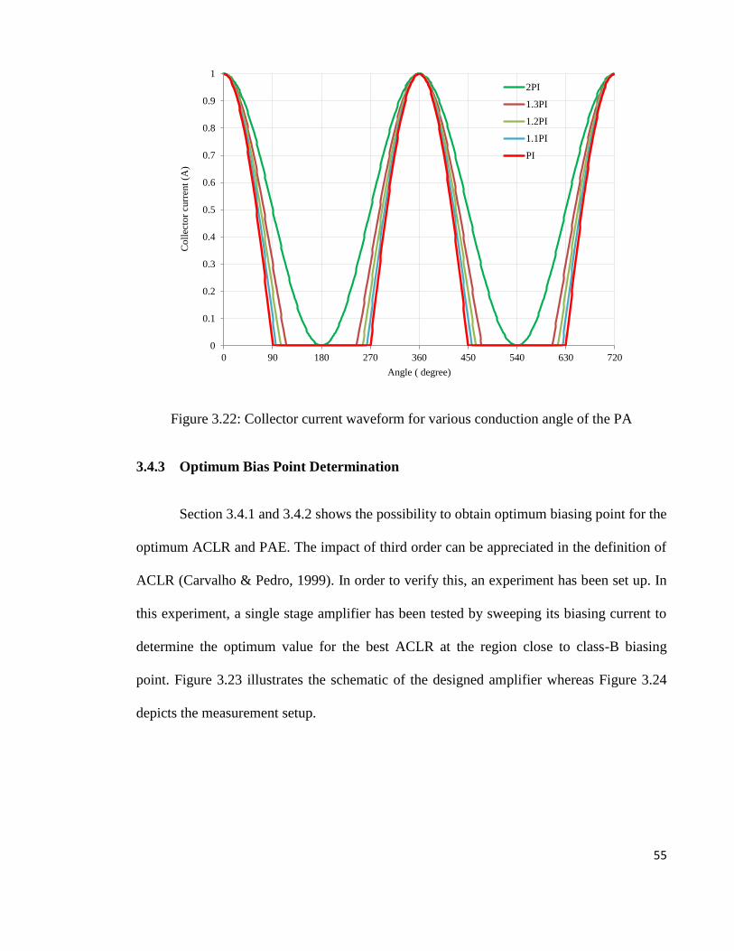
55
0
0.1
0.2
0.3
0.4
0.5
0.6
0.7
0.8
0.9
1
0 90 180 270 360 450 540 630 720
Co
llec
tor
curr
ent
(A)
Angle ( degree)
2PI
1.3PI
1.2PI
1.1PI
PI
Figure 3.22: Collector current waveform for various conduction angle of the PA
3.4.3 Optimum Bias Point Determination
Section 3.4.1 and 3.4.2 shows the possibility to obtain optimum biasing point for the
optimum ACLR and PAE. The impact of third order can be appreciated in the definition of
ACLR (Carvalho & Pedro, 1999). In order to verify this, an experiment has been set up. In
this experiment, a single stage amplifier has been tested by sweeping its biasing current to
determine the optimum value for the best ACLR at the region close to class-B biasing
point. Figure 3.23 illustrates the schematic of the designed amplifier whereas Figure 3.24
depicts the measurement setup.
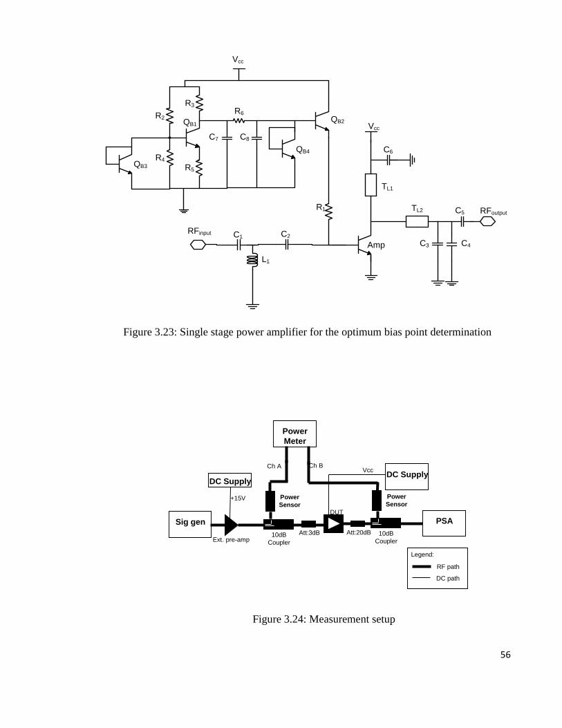
56
Vcc
Amp
C1
L1
RFoutput
RFinput C2
C6
TL1
TL2 C5
C3 C4
R1
QB2
R5
R3
R2
R4
QB1
QB3
QB4
R6
C7 C8
Vcc
Figure 3.23: Single stage power amplifier for the optimum bias point determination
10dB
Coupler
Ch A
Att:3dBExt. pre-amp
+15V
DC Supply
Power
Sensor
Power
Meter
Sig gen
DUT
Att:20dB
Ch B
10dB
Coupler
Power
Sensor
PSA
Legend:
RF path
DC path
DC Supply Vcc
Figure 3.24: Measurement setup
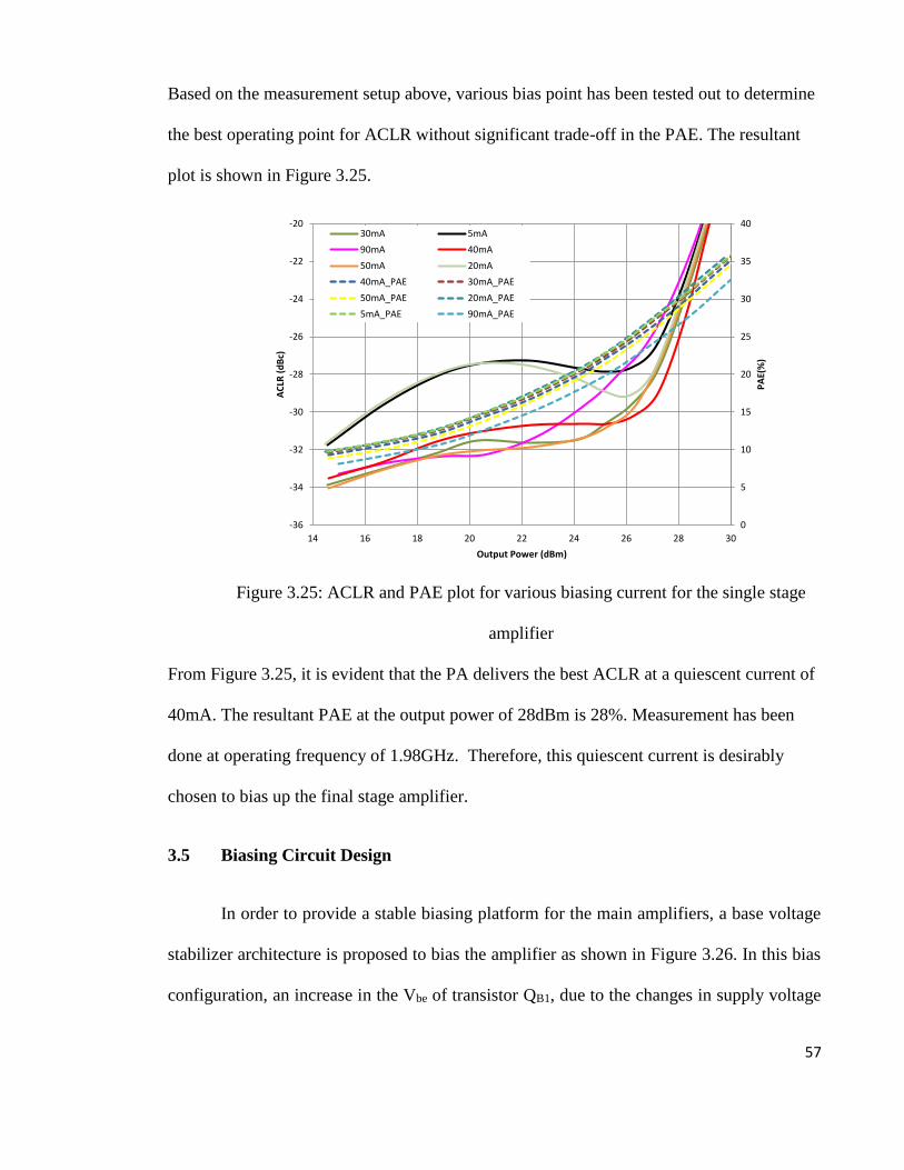
57
Based on the measurement setup above, various bias point has been tested out to determine
the best operating point for ACLR without significant trade-off in the PAE. The resultant
plot is shown in Figure 3.25.
0
5
10
15
20
25
30
35
40
-36
-34
-32
-30
-28
-26
-24
-22
-20
14 16 18 20 22 24 26 28 30
PA
E(%
)
AC
LR (
dB
c)
Output Power (dBm)
30mA 5mA
90mA 40mA
50mA 20mA
40mA_PAE 30mA_PAE
50mA_PAE 20mA_PAE
5mA_PAE 90mA_PAE
Figure 3.25: ACLR and PAE plot for various biasing current for the single stage
amplifier
From Figure 3.25, it is evident that the PA delivers the best ACLR at a quiescent current of
40mA. The resultant PAE at the output power of 28dBm is 28%. Measurement has been
done at operating frequency of 1.98GHz. Therefore, this quiescent current is desirably
chosen to bias up the final stage amplifier.
3.5 Biasing Circuit Design
In order to provide a stable biasing platform for the main amplifiers, a base voltage
stabilizer architecture is proposed to bias the amplifier as shown in Figure 3.26. In this bias
configuration, an increase in the Vbe of transistor QB1, due to the changes in supply voltage
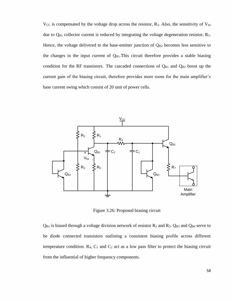
58
VCC is compensated by the voltage drop across the resistor, R3. Also, the sensitivity of Vbe
due to QB1 collector current is reduced by integrating the voltage degeneration resistor, R5.
Hence, the voltage delivered to the base-emitter junction of QB2 becomes less sensitive to
the changes in the input current of QB1.This circuit therefore provides a stable biasing
condition for the RF transistors. The cascaded connections of QB1 and QB2 boost up the
current gain of the biasing circuit, therefore provides more room for the main amplifier’s
base current swing which consist of 20 unit of power cells.
QB1 C2
VCC
C1
QB3 QB4
QB2
R1R2
R3 R5 R7
Main
Amplifier
R4
+
-Vbe
Figure 3.26: Proposed biasing circuit
QB1 is biased through a voltage division network of resistor R2 and R3. QB3 and QB4 serve to
be diode connected transistors outlining a consistent biasing profile across different
temperature condition. R4, C1 and C2 act as a low pass filter to protect the biasing circuit
from the influential of higher frequency components.

59
CHAPTER 4. DESIGN OF WIDEBAND EFFICIENCY POWER AMPLIFIER
4.1. Introduction
Efficiency is a critical parameter in power amplifier design. Primarily, the
conduction angle of the power amplifier marks the optimum operating point for a highly
efficient with reasonable trade-off in linearity. However, this is just not enough to fulfill the
specification requirement for handset operation as it operates at backed-off output power
where the efficiency is much lower.
In order to improve the efficiency of the PA, the voltage and current waveform is
manipulated. Figure 4.1 shows the voltage and current waveform for various classes of PA.
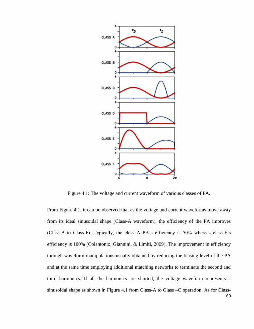
60
Figure 4.1: The voltage and current waveform of various classes of PA.
From Figure 4.1, it can be observed that as the voltage and current waveforms move away
from its ideal sinusoidal shape (Class-A waveform), the efficiency of the PA improves
(Class-B to Class-F). Typically, the class A PA’s efficiency is 50% whereas class-F’s
efficiency is 100% (Colantonio, Giannini, & Limiti, 2009). The improvement in efficiency
through waveform manipulations usually obtained by reducing the biasing level of the PA
and at the same time employing additional matching networks to terminate the second and
third harmonics. If all the harmonics are shorted, the voltage waveform represents a
sinusoidal shape as shown in Figure 4.1 from Class-A to Class –C operation. As for Class-
61
F, the efficiency is boosted by imparting the odd harmonics to the voltage waveform which
approximates a square wave (Raab, et al., 2002). Designing wideband harmonic resonators
to have wideband efficiency usually ends with trade off in the fundamental output power
(Tuffy, Zhu, & Brazil, 2011). As a result of this trade-off degradation in linear output
power is observed as well.
4.2. Class-J Power Amplifier – Theoretical Analysis
4.2.1. Fundamental of Class-J Design
The class-J PA was invented by S.C. Cripps (Cripps, RF Power Amplifiers for
Wireless Communications, 2006). It is capable of delivering the same efficiency and
linearity as with the class-AB power amplifier without the need of band limiting
transmission line harmonic short (Wright, Lees, Benedikt, Tasker, & Cripps, 2009).
Instead, it employs a reactance harmonic termination technique to achieve the efficiency
goal.
The conduction angle method to improve the efficiency of the power amplifier
focuses in modifying the current waveform. Modifying the current waveform from
sinusoidal (Class-A) to rectified sine wave (Class-B) increases the efficiency of the PA by
the factor of π/2 which can be proven with equation (3.38) in Chapter 3. However, in class-
J mode, the modification includes the voltage waveform as well which is explained through
the following analysis.
If the fundamental RF output power is given as:
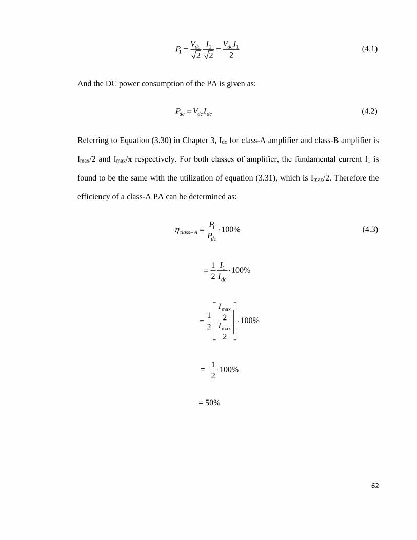
62
1 11
22 2
dc dcV I V IP (4.1)
And the DC power consumption of the PA is given as:
dc dc dcP V I (4.2)
Referring to Equation (3.30) in Chapter 3, Idc for class-A amplifier and class-B amplifier is
Imax/2 and Imax/π respectively. For both classes of amplifier, the fundamental current I1 is
found to be the same with the utilization of equation (3.31), which is Imax/2. Therefore the
efficiency of a class-A PA can be determined as:
1 100%class A
dc
P
P (4.3)
11100%
2 dc
I
I
max
max
1 2 100%2
2
I
I
= 1
100%2
= 50%
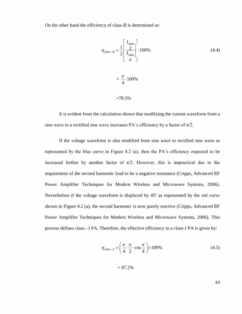
63
On the other hand the efficiency of class-B is determined as:
max
max
1 2 100%2
class B
I
I
(4.4)
= 100%4
=78.5%
It is evident from the calculation shown that modifying the current waveform from a
sine wave to a rectified sine wave increases PA’s efficiency by a factor of π/2.
If the voltage waveform is also modified from sine wave to rectified sine wave as
represented by the blue curve in Figure 4.2 (a), then the PA’s efficiency expected to be
increased further by another factor of π/2. However, this is impractical due to the
requirement of the second harmonic load to be a negative resistance (Cripps, Advanced RF
Power Amplifier Techniques for Modern Wireless and Microwave Systems, 2006).
Nevertheless if the voltage waveform is displaced by 45º as represented by the red curve
shown in Figure 4.2 (a), the second harmonic is now purely reactive (Cripps, Advanced RF
Power Amplifier Techniques for Modern Wireless and Microwave Systems, 2006). This
process defines class –J PA. Therefore, the effective efficiency in a class-J PA is given by:
cos 100%4 2 4
class J
(4.5)
= 87.2%
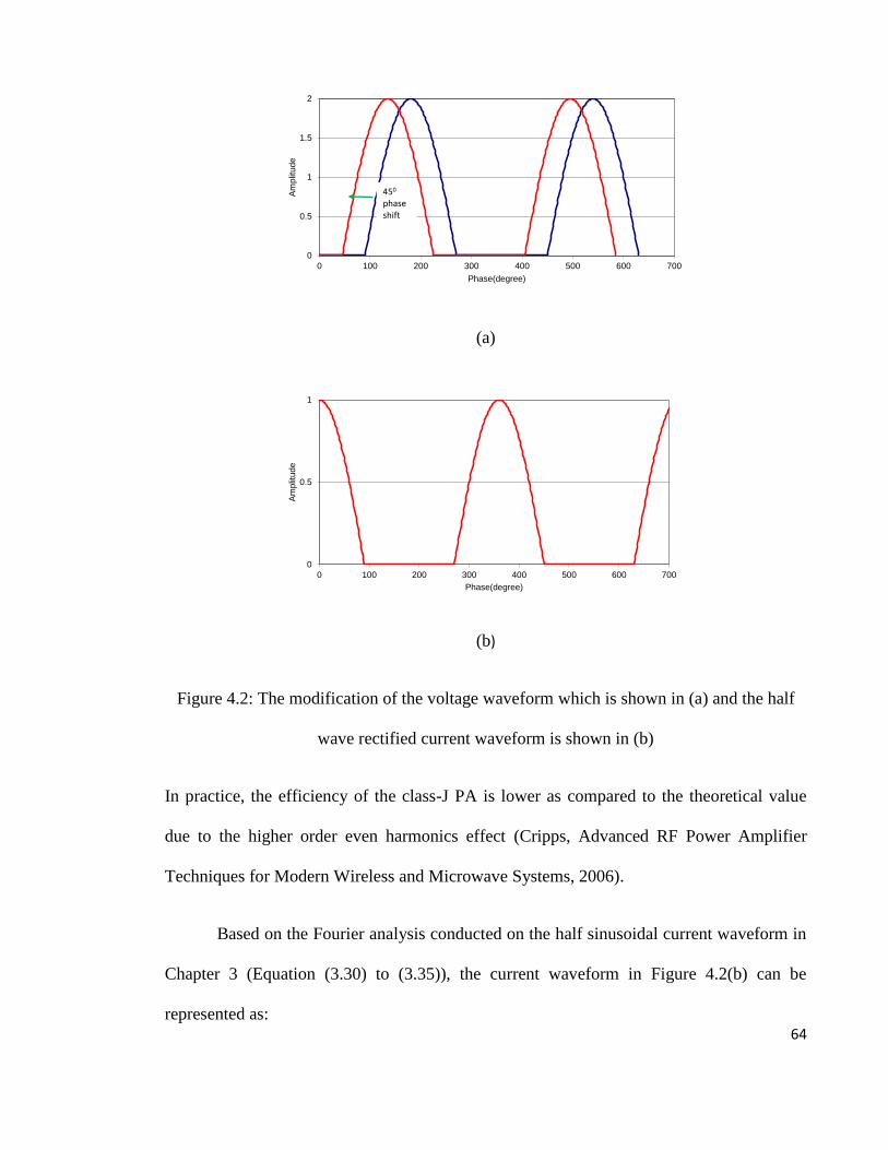
64
0
0.5
1
1.5
2
0 100 200 300 400 500 600 700
Am
plit
ude
Phase(degree)
450
phase shift
(a)
0
0.5
1
0 100 200 300 400 500 600 700
Am
plit
ud
e
Phase(degree)
(b)
Figure 4.2: The modification of the voltage waveform which is shown in (a) and the half
wave rectified current waveform is shown in (b)
In practice, the efficiency of the class-J PA is lower as compared to the theoretical value
due to the higher order even harmonics effect (Cripps, Advanced RF Power Amplifier
Techniques for Modern Wireless and Microwave Systems, 2006).
Based on the Fourier analysis conducted on the half sinusoidal current waveform in
Chapter 3 (Equation (3.30) to (3.35)), the current waveform in Figure 4.2(b) can be
represented as:
65
max
1 1 2( ) cos cos2 ......
2 3I I
(4.6)
whereas the shifted voltage waveform in Figure 4.2(a) is represented as:
1 1 2
( ) cos cos 2 .....2 3
dcV kV
………. (4.7)
where k is a constant with a value ≥ 2 which illustrates the class-J voltage waveform and δ
represents the shifted phase of the voltage waveform (Moon, Kim, & Kim, 2010). The load
impedance for each harmonic frequency can be calculated by:
nn
n
VZ
I (4.8)
Referring to Eq (4.6) and (4.7), if Imax =1 and k = π and the DC voltage is normalized to 1
by selecting k = π and Vdc= 1/π, the fundamental and second harmonic load impedances are
given as:
1 1Z (4.9)
2 1 2Z (4.10)
66
For class-J application, δ= π/4 rad. Therefore in rectangular form, equations (4.9) and
(4.10) can be represented as:
1
11
2Z j (4.11)
2Z j (4.12)
which shows presence of positive reactive component for the fundamental load impedance
and negative reactive component for the second harmonic, assuming the rest of the
harmonics are shorted.
The maximum value of the fundamental voltage of the class-J amplifier is increased
by factor of 2 above the class B amplifier. Therefore the fundamental load impedance is
set to optR2 where Ropt is the load impedance of the amplifier (Moon, Kim, & Kim, 2010).
On the other hand, in order to properly shape up the half-sinusoidal voltage waveform, the
ratio between second harmonic voltage waveform to fundamental voltage waveform is set
to 4
2 . Therefore:
0
2
2fV (4.13)
where Vfo is the fundamental voltage waveform. The ratio between the second harmonic
waveform (V2f0) to Vf0 is given as:
2 0
0
2
4
f
f
V
V
(4.14)
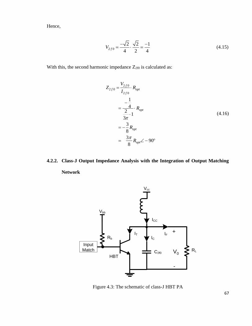
67
Hence,
2 0
2 2 1
4 2 4fV
(4.15)
With this, the second harmonic impedance Z2f0 is calculated as:
2 02 0
2 0
1
4 2
13
3
8
3 90
8
ff opt
f
opt
opt
opt
VZ R
I
R
R
R
(4.16)
4.2.2. Class-J Output Impedance Analysis with the Integration of Output Matching
Network
ICC
Vcc
Vbb
HBT
Rb
Input
Match
ICIT IF
RLC2f0 V0
+
-
Figure 4.3: The schematic of class-J HBT PA
68
Figure 4.3 depicts the schematic of the HBT class-J PA. The transistor is biased in class-B
mode where the RF output current waveform is half-wave rectified. Therefore:
max sinTI I for 0
= 0 for 2 (4.6)
The fundamental current component flowing in the matching network is given as:
1 sinFI I (4.7)
where ϕ is the phase deviation contributed by the matching network and I1 is fundamental
current.
The current flowing into C2f0 of Figure 4.3 is:
C CC F TI I I I (4.8)
where the DC output current, maxCC
II
.
The output voltage V0 is:
0
2 0 0
1C
f
V I dC
(4.9)
2 0 0
1C C
f
I d I dC
Therefore from conduction angle 0< θ<π,

69
max0 1 max
2 0 0
1sin sin
f
IV I I d
C
(4.10)
The solution for equation (4.10) is given in (4.11):
0 max 1
2 0
12 cos
f
V I IC
(4.11)
The negative sign means the voltage and current are out of phase to each other.
From conduction angle 0< θ<2π, IT of equation (4.8) is zero. Therefore:
max0 1
2 0 0
1sin
f
IV I d
C
(4.12)
where the resultant is given as:
max0 1
2 0
1cos cos
f
IV I
C
(4.13)
Fourier analysis is conducted on the output voltage to determine its fundamental and
second order components. The fundamental component is given as:
(4.14)
max
1
2 01
max
2 01
12sin cos sin 1
1
1 1sin cos sin 2 cos sin 1 cos2
2 4
1sin cos 2 1 cos
1
1 1 1cos 1 cos cos 1 cos2 sin sin 2
2 2 2
f
f
I
VC
I
I
jC
I
70
The second order component is:
max
2
2 0
1
1
2 0max
1 1 1 1sin 2 cos2 sin 2
2 4 41
1 1 1sin sin sin 3 sin 2 cos
3 6 2
1 1 1cos 1 cos2 cos 1 cos cos 1 cos3 sin sin sin 3 sin
2 3 31
1 1
2
f
f
I
VC
I
I
jC
I
sin 2 cos2 cos2 12
(4.15)
The full derivation of equation (4.10) to (4.15) is given in Appendix B. In equation (4.14)
and (4.15) it can be observed that the fundamental (V1) has a positive imaginary component
whereas the second order voltage (V2) has negative imaginary component. Therefore it can
be confirmed mathematically that the polarity of the imaginary components will not be
affected by the output matching network.
4.3 Simulation Analysis
As mentioned in Chapter 3, the Ropt is set to 5Ω which set to be optimum value for
maximum output power and PAE. Therefore, the initial 2nd harmonic reactive termination
capacitor value is calculated as below:
2 0
2 0
1
2f
f
CfZ
(4.18)
Since optf RZ8
302
and Ropt = 5Ω, at the highest operating frequency of 2GHz,
C2f0 = 13.5pF.
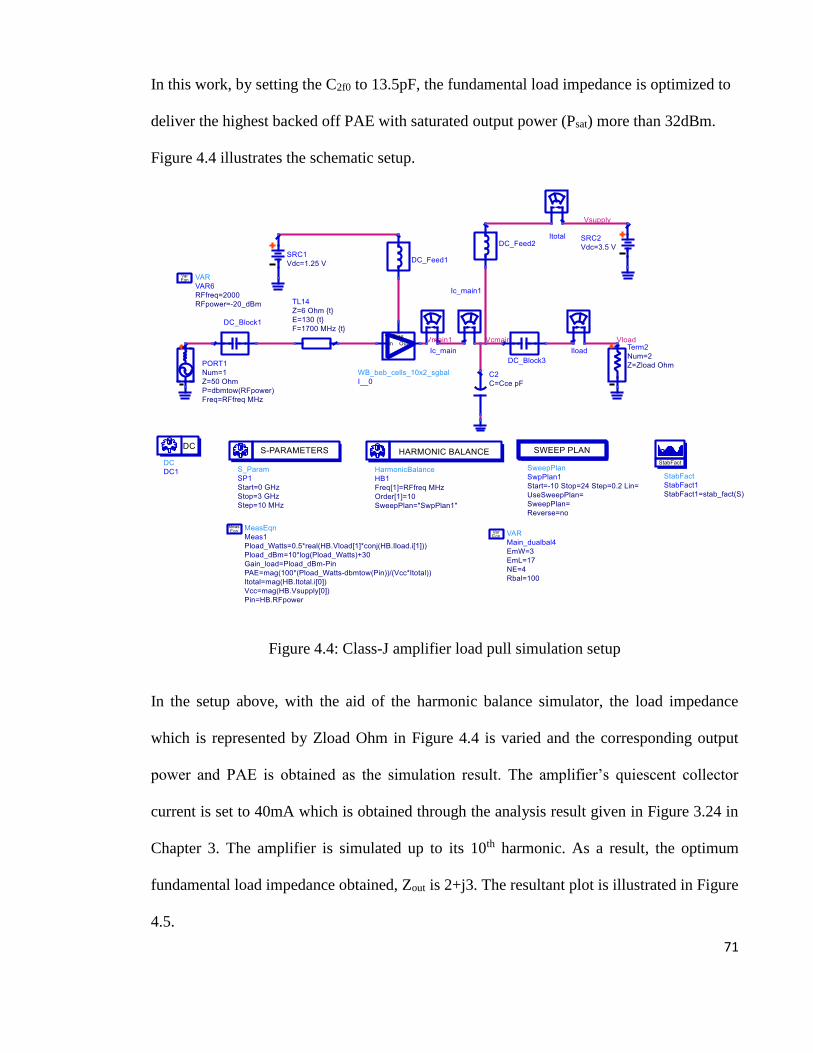
71
In this work, by setting the C2f0 to 13.5pF, the fundamental load impedance is optimized to
deliver the highest backed off PAE with saturated output power (Psat) more than 32dBm.
Figure 4.4 illustrates the schematic setup.
Figure 4.4: Class-J amplifier load pull simulation setup
In the setup above, with the aid of the harmonic balance simulator, the load impedance
which is represented by Zload Ohm in Figure 4.4 is varied and the corresponding output
power and PAE is obtained as the simulation result. The amplifier’s quiescent collector
current is set to 40mA which is obtained through the analysis result given in Figure 3.24 in
Chapter 3. The amplifier is simulated up to its 10th harmonic. As a result, the optimum
fundamental load impedance obtained, Zout is 2+j3. The resultant plot is illustrated in Figure
4.5.
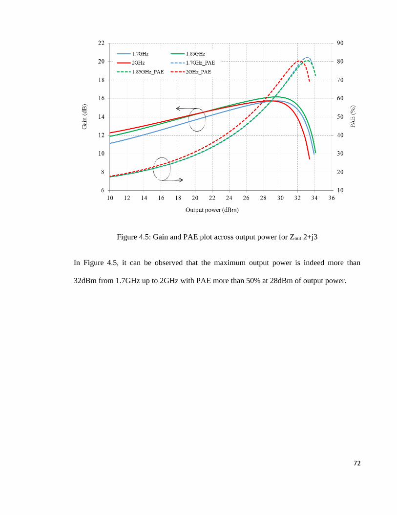
72
Figure 4.5: Gain and PAE plot across output power for Zout 2+j3
In Figure 4.5, it can be observed that the maximum output power is indeed more than
32dBm from 1.7GHz up to 2GHz with PAE more than 50% at 28dBm of output power.
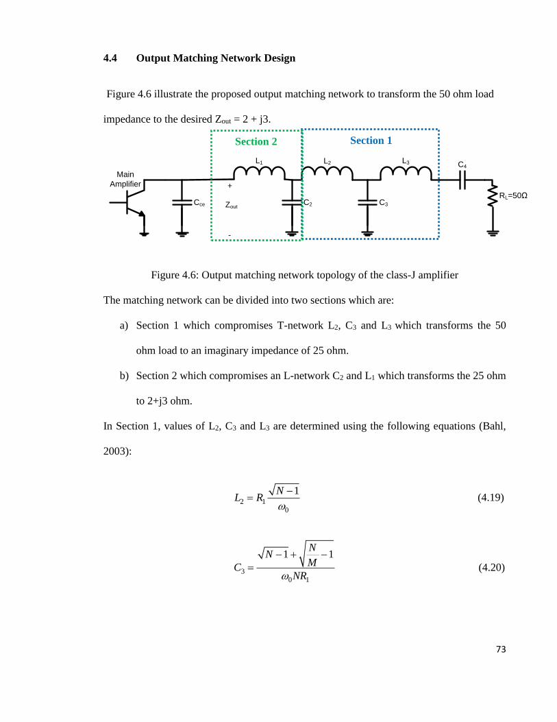
73
4.4 Output Matching Network Design
Figure 4.6 illustrate the proposed output matching network to transform the 50 ohm load
impedance to the desired Zout = 2 + j3.
L2
C3
L3 C4
C2
L1
Cce
RL=50Ω
+
-
Zout
Main
Amplifier
Figure 4.6: Output matching network topology of the class-J amplifier
The matching network can be divided into two sections which are:
a) Section 1 which compromises T-network L2, C3 and L3 which transforms the 50
ohm load to an imaginary impedance of 25 ohm.
b) Section 2 which compromises an L-network C2 and L1 which transforms the 25 ohm
to 2+j3 ohm.
In Section 1, values of L2, C3 and L3 are determined using the following equations (Bahl,
2003):
2 1
0
1NL R
(4.19)
3
0 1
1 1N
NMC
NR
(4.20)
Section 1 Section 2
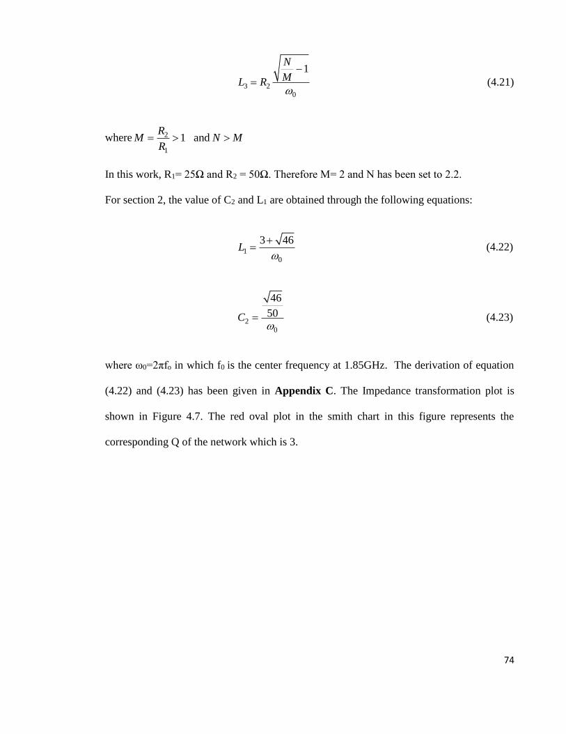
74
3 2
0
1N
ML R
(4.21)
where 2
1
1 and R
M N MR
In this work, R1= 25Ω and R2 = 50Ω. Therefore M= 2 and N has been set to 2.2.
For section 2, the value of C2 and L1 are obtained through the following equations:
1
0
3 46L
(4.22)
2
0
46
50C
(4.23)
where ω0=2πfo in which f0 is the center frequency at 1.85GHz. The derivation of equation
(4.22) and (4.23) has been given in Appendix C. The Impedance transformation plot is
shown in Figure 4.7. The red oval plot in the smith chart in this figure represents the
corresponding Q of the network which is 3.
75
Figure 4.7: Impedance Transformation Plot
Subsequently, L1, L2 and L3 are transformed to microstrip line using the following
equations (Bahl, Fundamentals of RF and Microwave Transistor Amplifiers, 2009):
0( / ) reZL H mm
c
(4.25)
where c is the speed of light, 3x10¹¹ mms-1. Ɛre can be determined using Eq. (4.26).
1 1( / )
2 2
r rre F W h
(4.26)
where F (W/h) is given as:
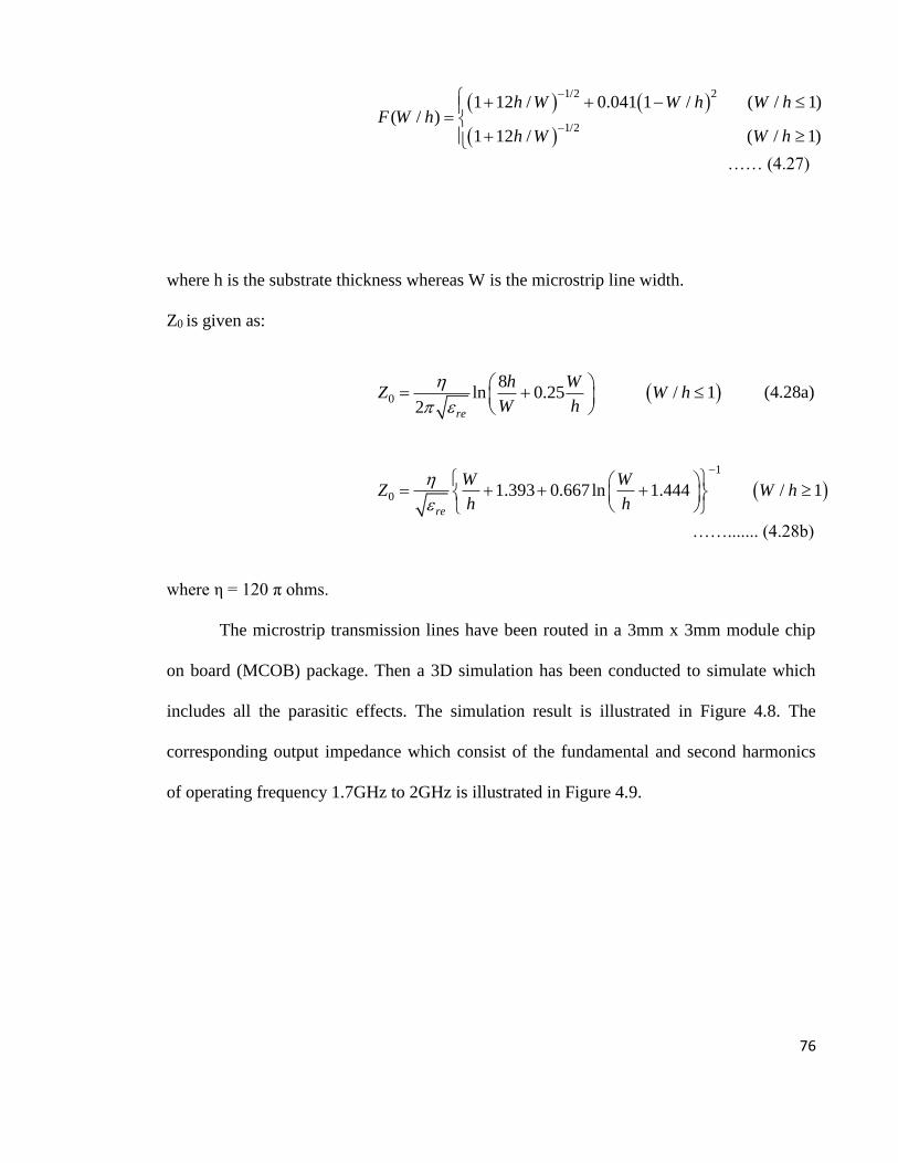
76
1/2 2
1/2
1 12 / 0.041 1 / ( / 1)( / )
1 12 / ( / 1)
h W W h W hF W h
h W W h
…… (4.27)
where h is the substrate thickness whereas W is the microstrip line width.
Z0 is given as:
0
8ln 0.25 / 1
2 re
h WZ W h
W h
(4.28a)
1
0 1.393 0.667ln 1.444 / 1re
W WZ W h
h h
……....... (4.28b)
where η = 120 π ohms.
The microstrip transmission lines have been routed in a 3mm x 3mm module chip
on board (MCOB) package. Then a 3D simulation has been conducted to simulate which
includes all the parasitic effects. The simulation result is illustrated in Figure 4.8. The
corresponding output impedance which consist of the fundamental and second harmonics
of operating frequency 1.7GHz to 2GHz is illustrated in Figure 4.9.
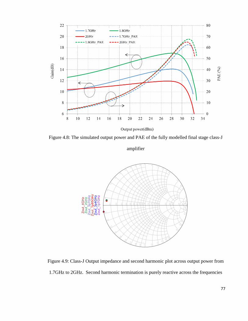
77
Figure 4.8: The simulated output power and PAE of the fully modelled final stage class-J
amplifier
Figure 4.9: Class-J Output impedance and second harmonic plot across output power from
1.7GHz to 2GHz. Second harmonic termination is purely reactive across the frequencies
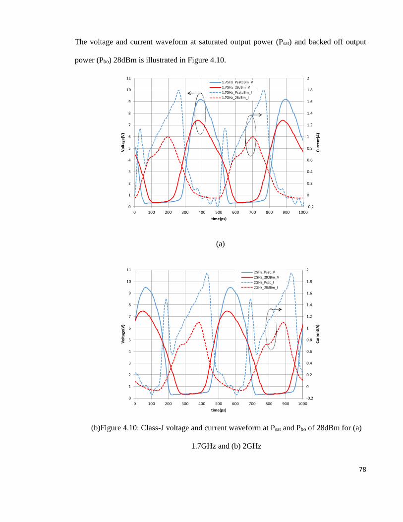
78
The voltage and current waveform at saturated output power (Psat) and backed off output
power (Pbo) 28dBm is illustrated in Figure 4.10.
-0.2
0
0.2
0.4
0.6
0.8
1
1.2
1.4
1.6
1.8
2
0
1
2
3
4
5
6
7
8
9
10
11
0 100 200 300 400 500 600 700 800 900 1000
Cu
rre
nt(
A)
Vo
ltag
e(V
)
time(ps)
1.7GHz_PsatdBm_V
1.7GHz_28dBm_V
1.7GHz_PsatdBm_I
1.7GHz_28dBm_I
(a)
-0.2
0
0.2
0.4
0.6
0.8
1
1.2
1.4
1.6
1.8
2
0
1
2
3
4
5
6
7
8
9
10
11
0 100 200 300 400 500 600 700 800 900 1000
Cu
rre
nt(
A)
Vo
ltag
e(V
)
time(ps)
2GHz_Psat_V
2GHz_28dBm_V
2GHz_Psat_I
2GHz_28dBm_I
(b)Figure 4.10: Class-J voltage and current waveform at Psat and Pbo of 28dBm for (a)
1.7GHz and (b) 2GHz

79
It can be observed in Figure 4.10 that the current waveform of Psat is bifurcated which
translates to a drop in PAE at output power more than 31dBm. This is known as bifurcation
phenomena (Cripps, RF Power Amplifiers for Wireless Communications, 2006). This issue
can be minimized if the supply voltage of the PA is increased.
80
CHAPTER 5. ANALOG PRE-DISTORTER DESIGN AND THE REALIZATION
OF HIGH GAIN POWER AMPLIFIER
5.1. Introduction
The goal of the linearization technique in this work is to reduce the back-off output
power level due to PAPR backlash, thus exhibiting higher linear output power with low
quiescent current. This is accomplished by integrating an analog pre-distorter (APD) block
at the input of the low voltage main amplifier in the proposed architecture.
Operating the main amplifier at low quiescent current headroom results into gain
expansion phenomena. This is due to the rise of the third order intermodulation distortion
(IMD3) component as the output power increases (Carvalho & Pedro, 1999). The rise of the
third order nonlinearity significantly degrades the ACLR (Carvalho & Pedro, Compact
Formulas to Relate ACPR and NPR to Two Tone IMR and IP3, 1999). In order to mitigate
this adverse effect, the APD architecture is integrated to produce IMD3 components, which
are equal in amplitude but 180o out-of-phase respective to the IMD3 spurs generated by the
main amplifier. Thus, the IMD3 cancellation attained extends the overall linear output
power span of the PA.
Finally, in order to boost up the power gain to be more than 30dB, a pre-driver
amplifier is cascaded to the class-J PA with a built in APD. A higher gain cannot be
achieved with a single stage amplifier due to the technology constraint whereby as the
output power of the amplifier increases the power gain will be lower (Gilmore & Besser,
2003). The inter-stage matching network between the pre-driver amplifier and the APD
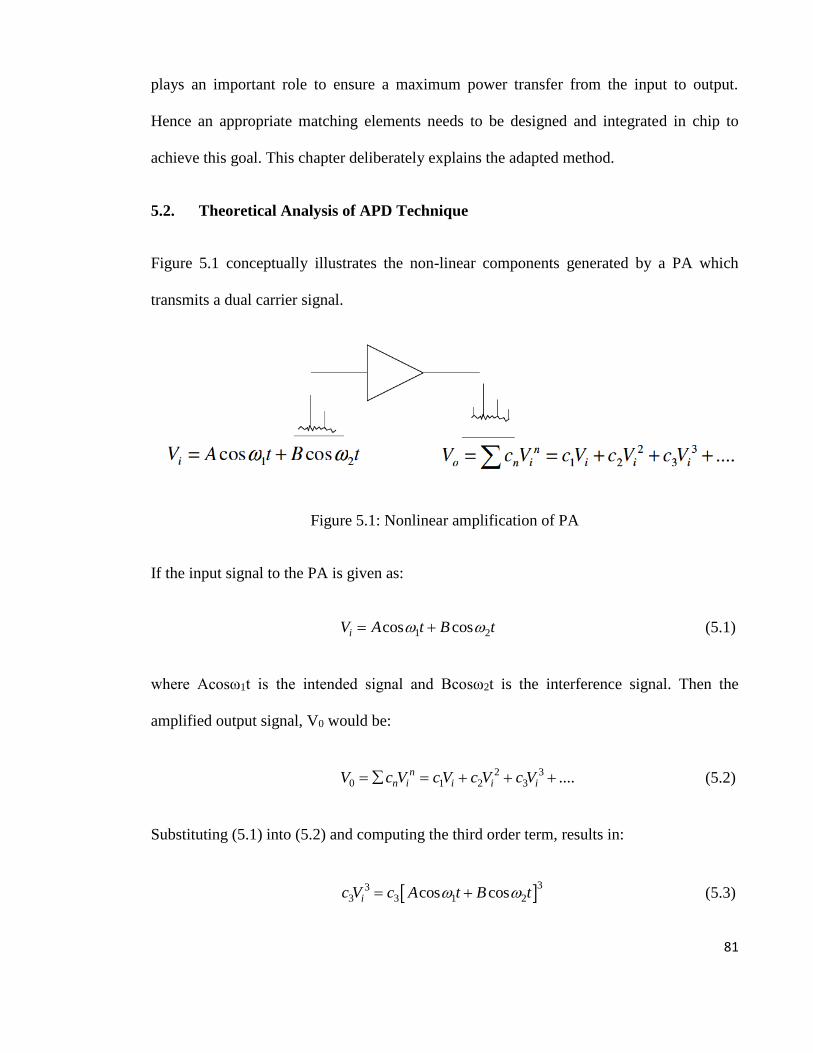
81
plays an important role to ensure a maximum power transfer from the input to output.
Hence an appropriate matching elements needs to be designed and integrated in chip to
achieve this goal. This chapter deliberately explains the adapted method.
5.2. Theoretical Analysis of APD Technique
Figure 5.1 conceptually illustrates the non-linear components generated by a PA which
transmits a dual carrier signal.
Figure 5.1: Nonlinear amplification of PA
If the input signal to the PA is given as:
1 2cos cosiV A t B t (5.1)
where Acosω1t is the intended signal and Bcosω2t is the interference signal. Then the
amplified output signal, V0 would be:
2 30 1 2 3 ....n
n i i i iV c V c V c V c V (5.2)
Substituting (5.1) into (5.2) and computing the third order term, results in:
33
3 3 1 2cos cosic V c A t B t (5.3)
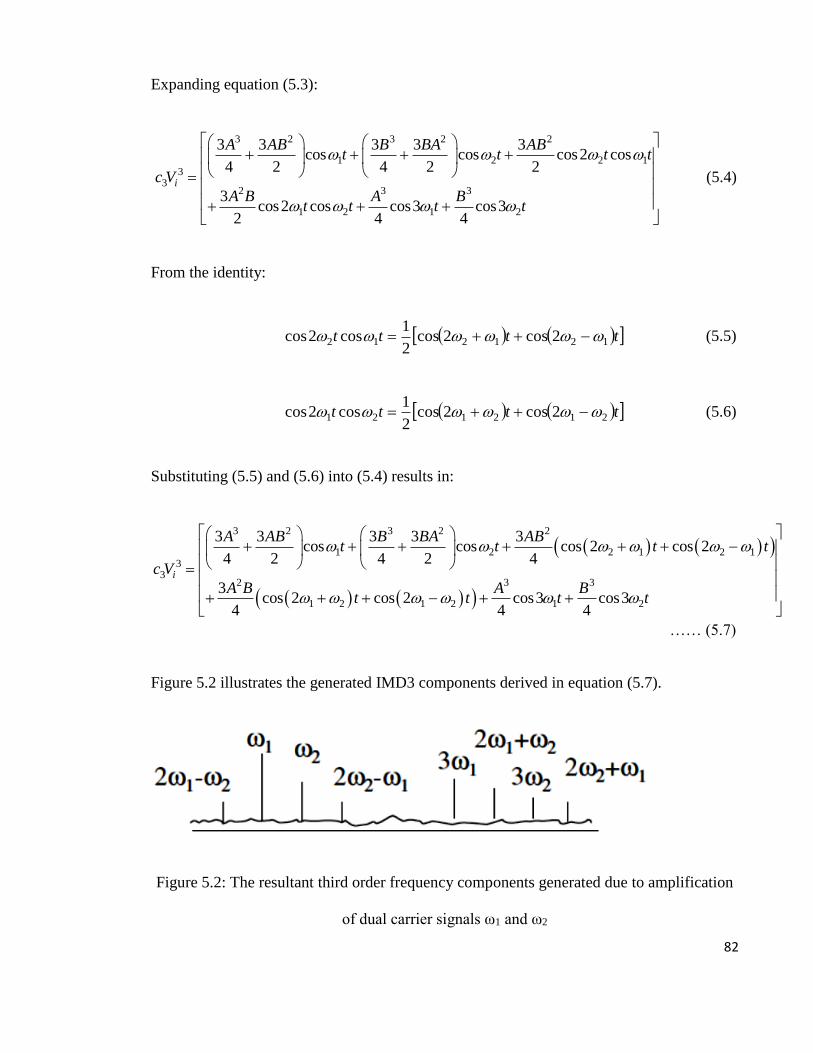
82
Expanding equation (5.3):
3 2 3 2 2
1 2 2 13
32 3 3
1 2 1 2
3 3 3 3 3cos cos cos2 cos
4 2 4 2 2
3cos2 cos cos3 cos3
2 4 4
i
A AB B BA ABt t t t
c V
A B A Bt t t t
(5.4)
From the identity:
tttt 121212 2cos2cos2
1cos2cos (5.5)
tttt 212121 2cos2cos2
1cos2cos (5.6)
Substituting (5.5) and (5.6) into (5.4) results in:
3 2 3 2 2
1 2 2 1 2 13
32 3 3
1 2 1 2 1 2
3 3 3 3 3cos cos cos 2 cos 2
4 2 4 2 4
3cos 2 cos 2 cos3 cos3
4 4 4
i
A AB B BA ABt t t t
c V
A B A Bt t t t
…… (5.7)
Figure 5.2 illustrates the generated IMD3 components derived in equation (5.7).
Figure 5.2: The resultant third order frequency components generated due to amplification
of dual carrier signals ω1 and ω2
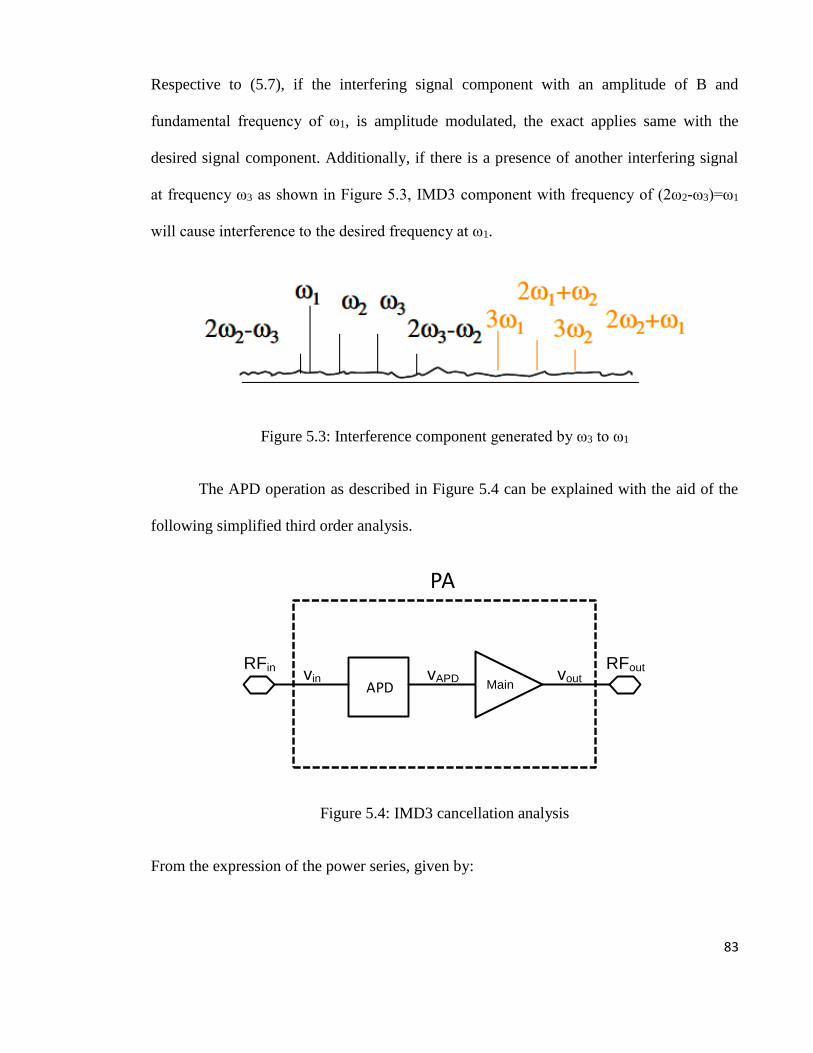
83
Respective to (5.7), if the interfering signal component with an amplitude of B and
fundamental frequency of ω1, is amplitude modulated, the exact applies same with the
desired signal component. Additionally, if there is a presence of another interfering signal
at frequency ω3 as shown in Figure 5.3, IMD3 component with frequency of (2ω2-ω3)=ω1
will cause interference to the desired frequency at ω1.
Figure 5.3: Interference component generated by ω3 to ω1
The APD operation as described in Figure 5.4 can be explained with the aid of the
following simplified third order analysis.
vAPDvin APD
&
Driver
Main
RFin RFoutvout
PA
APD
Figure 5.4: IMD3 cancellation analysis
From the expression of the power series, given by:
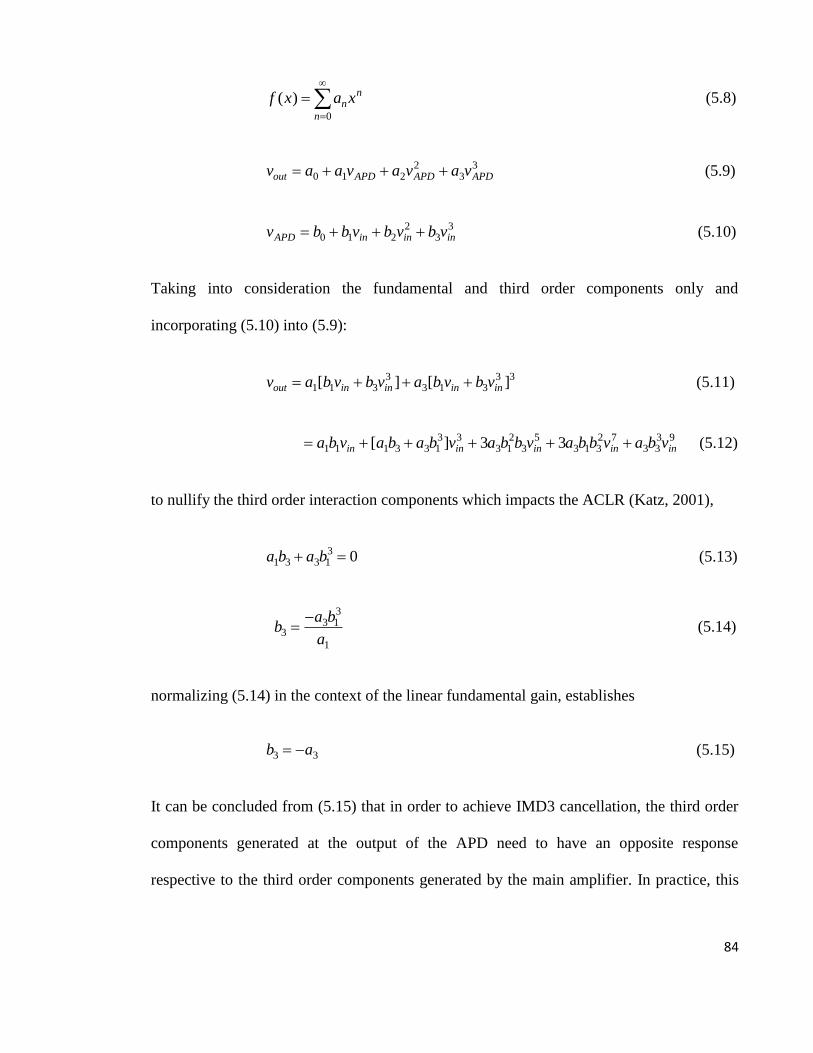
84
0
( ) nn
n
f x a x
(5.8)
2 30 1 2 3out APD APD APDv a a v a v a v (5.9)
2 30 1 2 3APD in in inv b b v b v b v (5.10)
Taking into consideration the fundamental and third order components only and
incorporating (5.10) into (5.9):
3 3 31 1 3 3 1 3[ ] [ ]out in in in inv a b v b v a b v b v (5.11)
3 3 2 5 2 7 3 91 1 1 3 3 1 3 1 3 3 1 3 3 3[ ] 3 3in in in in ina b v a b a b v a b b v a b b v a b v (5.12)
to nullify the third order interaction components which impacts the ACLR (Katz, 2001),
31 3 3 1 0a b a b (5.13)
3
3 13
1
a bb
a
(5.14)
normalizing (5.14) in the context of the linear fundamental gain, establishes
3 3b a (5.15)
It can be concluded from (5.15) that in order to achieve IMD3 cancellation, the third order
components generated at the output of the APD need to have an opposite response
respective to the third order components generated by the main amplifier. In practice, this
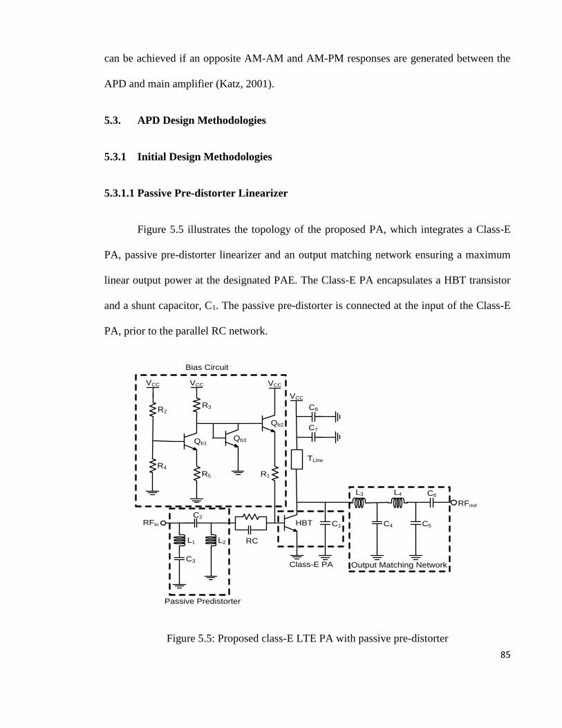
85
can be achieved if an opposite AM-AM and AM-PM responses are generated between the
APD and main amplifier (Katz, 2001).
5.3. APD Design Methodologies
5.3.1 Initial Design Methodologies
5.3.1.1 Passive Pre-distorter Linearizer
Figure 5.5 illustrates the topology of the proposed PA, which integrates a Class-E
PA, passive pre-distorter linearizer and an output matching network ensuring a maximum
linear output power at the designated PAE. The Class-E PA encapsulates a HBT transistor
and a shunt capacitor, C1. The passive pre-distorter is connected at the input of the Class-E
PA, prior to the parallel RC network.
C4HBT C5
L4
RFout
Output Matching Network
RC
C1
C7
TLine
C8
L2
RFin
L1
C2
R1R5
R3R2
R4
VCCVCCVCC
VCC
L3 C6
Class-E PA
Passive Predistorter
Bias Circuit
C3
Qb1
Qb2
Qb3
Figure 5.5: Proposed class-E LTE PA with passive pre-distorter
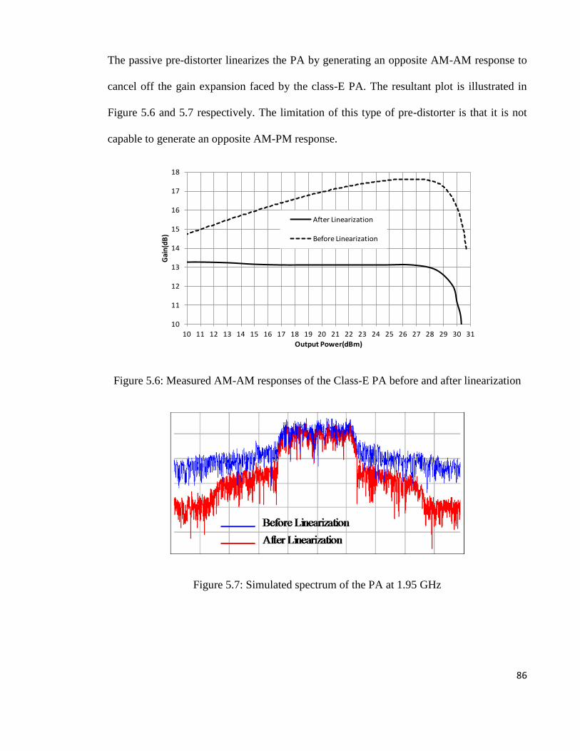
86
The passive pre-distorter linearizes the PA by generating an opposite AM-AM response to
cancel off the gain expansion faced by the class-E PA. The resultant plot is illustrated in
Figure 5.6 and 5.7 respectively. The limitation of this type of pre-distorter is that it is not
capable to generate an opposite AM-PM response.
10
11
12
13
14
15
16
17
18
10 11 12 13 14 15 16 17 18 19 20 21 22 23 24 25 26 27 28 29 30 31
Gai
n(d
B)
Output Power(dBm)
After Linearization
Before Linearization
Figure 5.6: Measured AM-AM responses of the Class-E PA before and after linearization
Figure 5.7: Simulated spectrum of the PA at 1.95 GHz
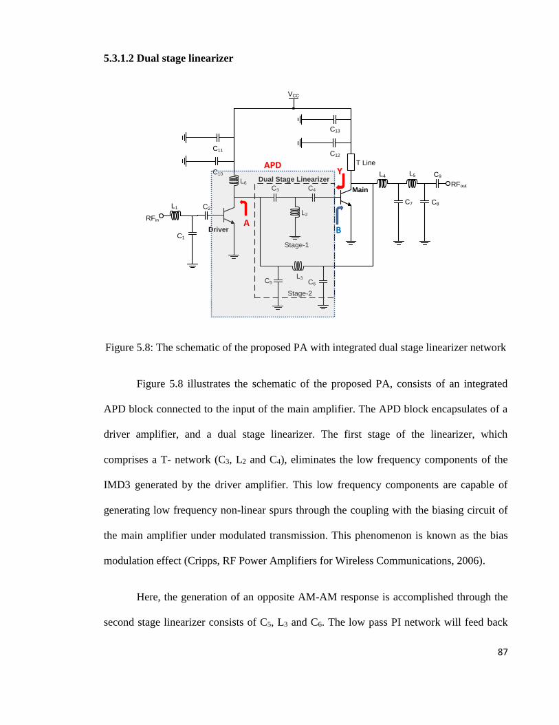
87
5.3.1.2 Dual stage linearizer
RFin
L1
C1
L6
Driver
C10
C11
C3
L2
C12
C13
C4
C7
L4 L5
C8
RFoutMain
VCC
C2
C9
T Line
L3
Stage-1
Stage-2
C5 C6
Dual Stage LinearizerY
APD
AB
Figure 5.8: The schematic of the proposed PA with integrated dual stage linearizer network
Figure 5.8 illustrates the schematic of the proposed PA, consists of an integrated
APD block connected to the input of the main amplifier. The APD block encapsulates of a
driver amplifier, and a dual stage linearizer. The first stage of the linearizer, which
comprises a T- network (C3, L2 and C4), eliminates the low frequency components of the
IMD3 generated by the driver amplifier. This low frequency components are capable of
generating low frequency non-linear spurs through the coupling with the biasing circuit of
the main amplifier under modulated transmission. This phenomenon is known as the bias
modulation effect (Cripps, RF Power Amplifiers for Wireless Communications, 2006).
Here, the generation of an opposite AM-AM response is accomplished through the
second stage linearizer consists of C5, L3 and C6. The low pass PI network will feed back
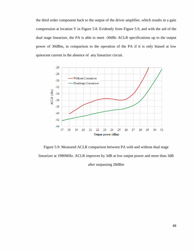
88
the third order component back to the output of the driver amplifier, which results in a gain
compression at location Y in Figure 5.8. Evidently from Figure 5.9, and with the aid of the
dual stage linearizer, the PA is able to meet -30dBc ACLR specifications up to the output
power of 30dBm, in comparison to the operation of the PA if it is only biased at low
quiescent current in the absence of any linearizer circuit.
Figure 5.9: Measured ACLR comparison between PA with and without dual stage
linearizer at 1980MHz. ACLR improves by 3dB at low output power and more than 3dB
after surpassing 28dBm
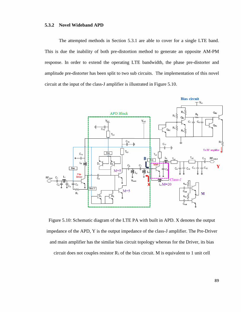
89
5.3.2 Novel Wideband APD
The attempted methods in Section 5.3.1 are able to cover for a single LTE band.
This is due the inability of both pre-distortion method to generate an opposite AM-PM
response. In order to extend the operating LTE bandwidth, the phase pre-distorter and
amplitude pre-distorter has been split to two sub circuits. The implementation of this novel
circuit at the input of the class-J amplifier is illustrated in Figure 5.10.
Figure 5.10: Schematic diagram of the LTE PA with built in APD. X denotes the output
impedance of the APD, Y is the output impedance of the class-J amplifier. The Pre-Driver
and main amplifier has the similar bias circuit topology whereas for the Driver, its bias
circuit does not couples resistor R1 of the bias circuit. M is equivalent to 1 unit cell
Y
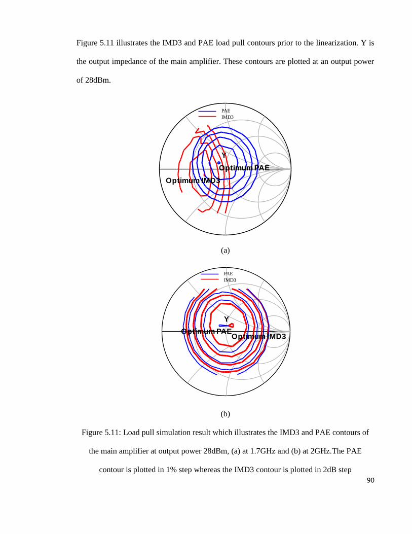
90
Figure 5.11 illustrates the IMD3 and PAE load pull contours prior to the linearization. Y is
the output impedance of the main amplifier. These contours are plotted at an output power
of 28dBm.
indep(ThirdOrdIMD_contours_p) (0.000 to 31.000)
Thir
dO
rdIM
D_conto
urs
_p
indep(PAE_contours_p) (0.000 to 36.000)
PA
E_conto
urs
_p
Y
Optimum PAE
Optimum IMD3
PAE
IMD3
(a)
indep(PAE_contours_p) (0.000 to 37.000)
PA
E_
co
nto
urs
_p
indep(Pdel_contours_p) (0.000 to 37.000)
Pd
el_
co
nto
urs
_p
Y
PAE
IMD3
Optimum PAEOptimum IMD3
(b)
Figure 5.11: Load pull simulation result which illustrates the IMD3 and PAE contours of
the main amplifier at output power 28dBm, (a) at 1.7GHz and (b) at 2GHz.The PAE
contour is plotted in 1% step whereas the IMD3 contour is plotted in 2dB step
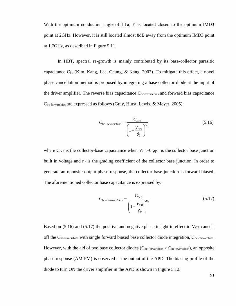
91
With the optimum conduction angle of 1.1π, Y is located closed to the optimum IMD3
point at 2GHz. However, it is still located almost 8dB away from the optimum IMD3 point
at 1.7GHz, as described in Figure 5.11.
In HBT, spectral re-growth is mainly contributed by its base-collector parasitic
capacitance Cbc (Kim, Kang, Lee, Chung, & Kang, 2002). To mitigate this effect, a novel
phase cancellation method is proposed by integrating a base collector diode at the input of
the driver amplifier. The reverse bias capacitance Cbc-reversebias and forward bias capacitance
Cbc-forwardbias are expressed as follows (Gray, Hurst, Lewis, & Meyer, 2005):
0
0
1
c
bcbc reversebias n
CB
CC
V
f
(5.16)
where Cbc0 is the collector-base capacitance when VCB=0 ,φ0 is the collector base junction
built in voltage and nc is the grading coefficient of the collector base junction. In order to
generate an opposite output phase response, the collector-base junction is forward biased.
The aforementioned collector base capacitance is expressed by:
0
0
1
c
bcbc forwardbias n
CB
CC
V
f
(5.17)
Based on (5.16) and (5.17) the positive and negative phase insight in effect to VCB cancels
off the Cbc-reversebias with single forward biased base collector diode integration, Cbc-forwardbias.
However, with the aid of two base collector diodes (Cbc-forwardbias > Cbc-reversebias), an opposite
phase response (AM-PM) is observed at the output of the APD. The biasing profile of the
diode to turn ON the driver amplifier in the APD is shown in Figure 5.12.
92
0
20
40
60
80
100
120
140
160
180
200
0 0.2 0.4 0.6 0.8 1 1.2 1.4 1.6 1.8 2 2.2 2.4 2.6
Dri
ver
Co
llect
or
Cu
rre
nt,
I c(m
A)
Diode voltage,VD(V)
Figure 5.12: Biasing profile of the integrated parallel base collector diodes. The supply
voltage to the diodes has to be at least 2.2V to turn ON the driver stage
The simulated AM-PM response at the output of the APD and class-J main amplifier are
illustrated in Figure 5.13.
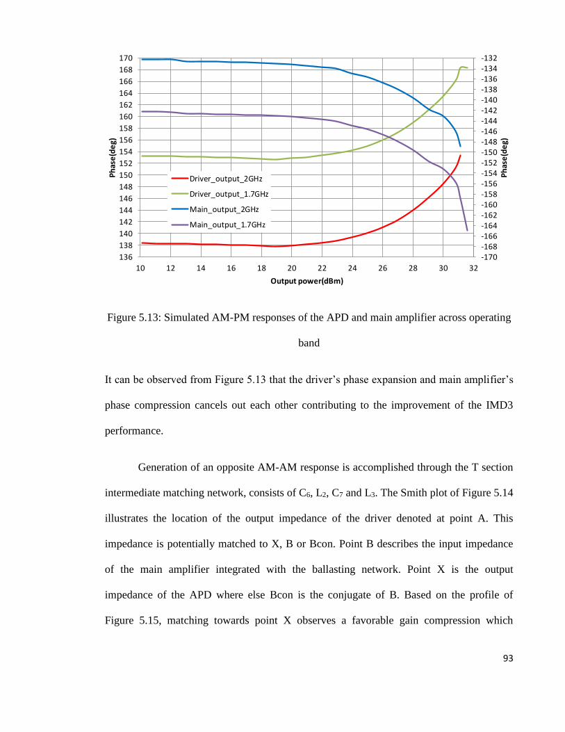
93
-170-168-166-164-162-160-158-156-154-152-150-148-146-144-142-140-138-136-134-132
136
138
140
142
144
146
148
150
152
154
156
158
160
162
164
166
168
170
10 12 14 16 18 20 22 24 26 28 30 32
Ph
ase
(de
g)
Ph
ase
(de
g)
Output power(dBm)
Driver_output_2GHz
Driver_output_1.7GHz
Main_output_2GHz
Main_output_1.7GHz
Figure 5.13: Simulated AM-PM responses of the APD and main amplifier across operating
band
It can be observed from Figure 5.13 that the driver’s phase expansion and main amplifier’s
phase compression cancels out each other contributing to the improvement of the IMD3
performance.
Generation of an opposite AM-AM response is accomplished through the T section
intermediate matching network, consists of C6, L2, C7 and L3. The Smith plot of Figure 5.14
illustrates the location of the output impedance of the driver denoted at point A. This
impedance is potentially matched to X, B or Bcon. Point B describes the input impedance
of the main amplifier integrated with the ballasting network. Point X is the output
impedance of the APD where else Bcon is the conjugate of B. Based on the profile of
Figure 5.15, matching towards point X observes a favorable gain compression which
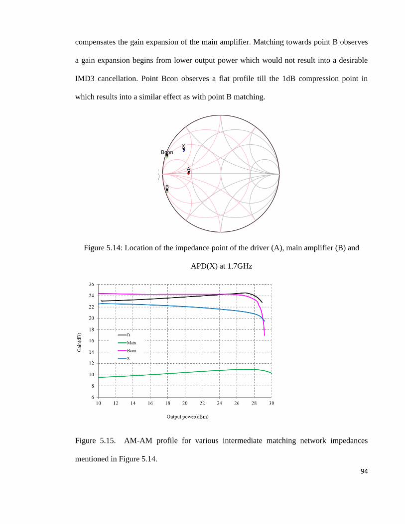
94
compensates the gain expansion of the main amplifier. Matching towards point B observes
a gain expansion begins from lower output power which would not result into a desirable
IMD3 cancellation. Point Bcon observes a flat profile till the 1dB compression point in
which results into a similar effect as with point B matching.
A-Driver outputB-Main input( including ballast cct)
RFpower (-6.000 to -6.000)
Z_
IMP
Readout
A
Readout
B
Readout
X
Readout
Bcon
ARFpower=Zout_drv=0.551 / 179.056impedance = 14.484 + j0.377
-6.000
BRFpower=Zin_main=0.970 / -162.144impedance = 0.784 - j7.853
-6.000
XRFpower=Zout_ITS1=0.756 / 147.687impedance = 7.503 + j14.184
-6.000
BconRFpower=Zin_main_conj=0.970 / 162.144impedance = 0.784 + j7.853
-6.000
Figure 5.14: Location of the impedance point of the driver (A), main amplifier (B) and
APD(X) at 1.7GHz
Figure 5.15. AM-AM profile for various intermediate matching network impedances
mentioned in Figure 5.14.
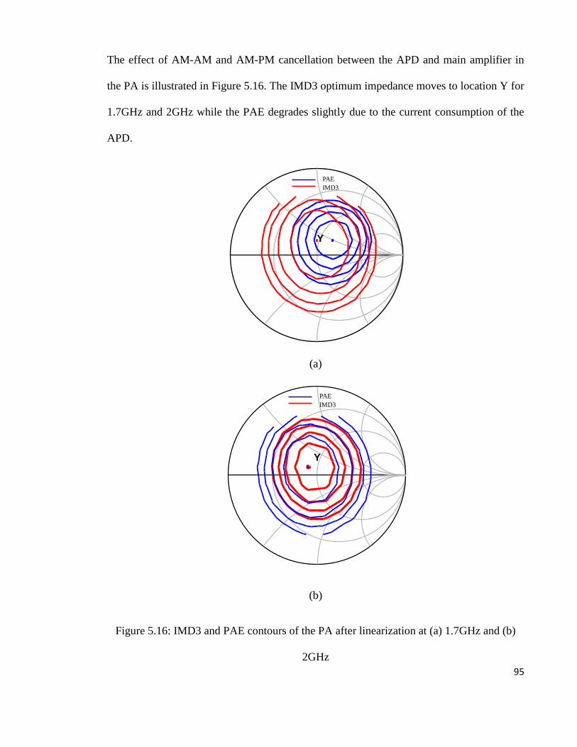
95
The effect of AM-AM and AM-PM cancellation between the APD and main amplifier in
the PA is illustrated in Figure 5.16. The IMD3 optimum impedance moves to location Y for
1.7GHz and 2GHz while the PAE degrades slightly due to the current consumption of the
APD.
indep(PAE_contours_p) (0.000 to 38.000)
PA
E_conto
urs
_p
indep(Pdel_contours_p) (0.000 to 43.000)
Pdel_
conto
urs
_p
Y
PAE
IMD3
(a)
indep(PAE_contours_p) (0.000 to 36.000)
PA
E_
co
nto
urs
_p
indep(Pdel_contours_p) (0.000 to 39.000)
Pd
el_
co
nto
urs
_p
Y
PAE
IMD3
(b)
Figure 5.16: IMD3 and PAE contours of the PA after linearization at (a) 1.7GHz and (b)
2GHz
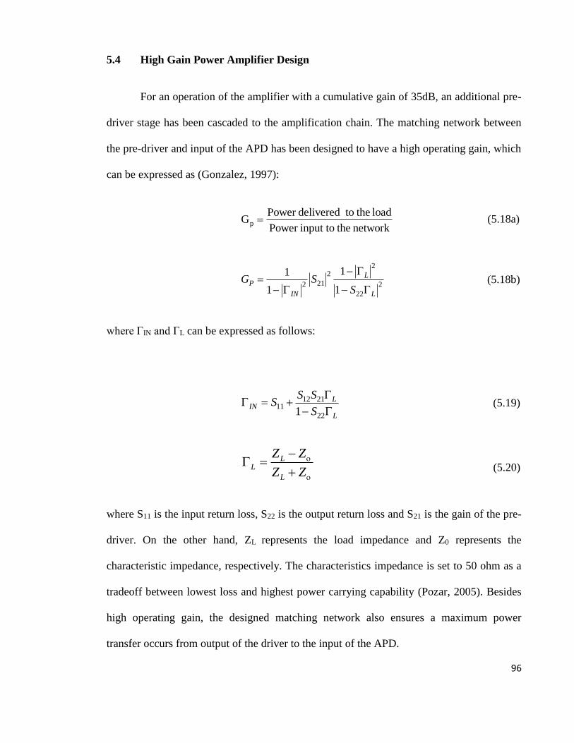
96
5.4 High Gain Power Amplifier Design
For an operation of the amplifier with a cumulative gain of 35dB, an additional pre-
driver stage has been cascaded to the amplification chain. The matching network between
the pre-driver and input of the APD has been designed to have a high operating gain, which
can be expressed as (Gonzalez, 1997):
p
Power delivered to the loadG
Power input to the network (5.18a)
22
212 2
22
11
11
LP
LIN
G SS
(5.18b)
where ΓIN and ΓL can be expressed as follows:
12 2111
221
LIN
L
S SS
S
(5.19)
LL
L
Z Z
Z Z
(5.20)
where S11 is the input return loss, S22 is the output return loss and S21 is the gain of the pre-
driver. On the other hand, ZL represents the load impedance and Z0 represents the
characteristic impedance, respectively. The characteristics impedance is set to 50 ohm as a
tradeoff between lowest loss and highest power carrying capability (Pozar, 2005). Besides
high operating gain, the designed matching network also ensures a maximum power
transfer occurs from output of the driver to the input of the APD.

97
Another important parameter which has been given priority in this paper is the
unconditional stability factor, which known the Rollett factor, K (Rollett, 1962). The power
amplifier has been designed to meet this criterion, which is conditioned as (Ludwig &
Bretchko, 2000):-
2 2 2
11 22 11 22 12 21
12 21
11
2
S S S S S SK
S S
(5.21)
Besides the above mentioned stability factor, the source and load stability circles of the
integrated PA has also been plotted to ensure it is located outside the Smith chart to operate
in unconditional stability mode. The plots are reviewed in Chapter 6.
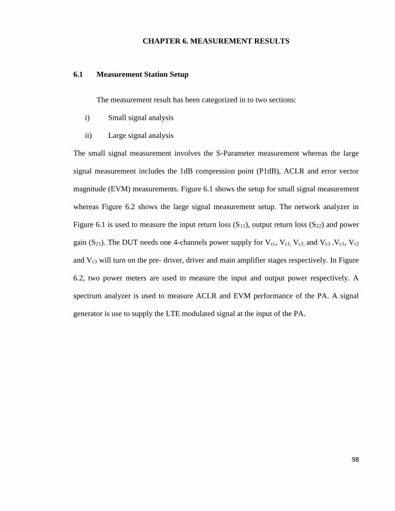
98
CHAPTER 6. MEASUREMENT RESULTS
6.1 Measurement Station Setup
The measurement result has been categorized in to two sections:
i) Small signal analysis
ii) Large signal analysis
The small signal measurement involves the S-Parameter measurement whereas the large
signal measurement includes the 1dB compression point (P1dB), ACLR and error vector
magnitude (EVM) measurements. Figure 6.1 shows the setup for small signal measurement
whereas Figure 6.2 shows the large signal measurement setup. The network analyzer in
Figure 6.1 is used to measure the input return loss (S11), output return loss (S22) and power
gain (S21). The DUT needs one 4-channels power supply for Vcc, Vc1, Vc2, and Vc3 .Vc1, Vc2
and Vc3 will turn on the pre- driver, driver and main amplifier stages respectively. In Figure
6.2, two power meters are used to measure the input and output power respectively. A
spectrum analyzer is used to measure ACLR and EVM performance of the PA. A signal
generator is use to supply the LTE modulated signal at the input of the PA.
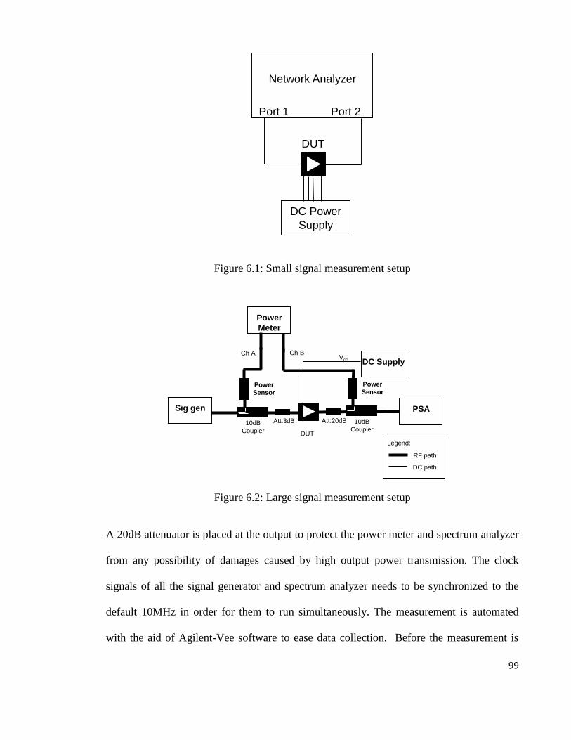
99
Network Analyzer
Port 1 Port 2
DUT
DC Power
Supply
Figure 6.1: Small signal measurement setup
10dB
Coupler
Ch A
Att:3dB
Power
Sensor
Power
Meter
Sig gen
DUT
Att:20dB
Ch B
10dB
Coupler
Power
Sensor
PSA
Legend:
RF path
DC path
DC Supply Vcc
Figure 6.2: Large signal measurement setup
A 20dB attenuator is placed at the output to protect the power meter and spectrum analyzer
from any possibility of damages caused by high output power transmission. The clock
signals of all the signal generator and spectrum analyzer needs to be synchronized to the
default 10MHz in order for them to run simultaneously. The measurement is automated
with the aid of Agilent-Vee software to ease data collection. Before the measurement is
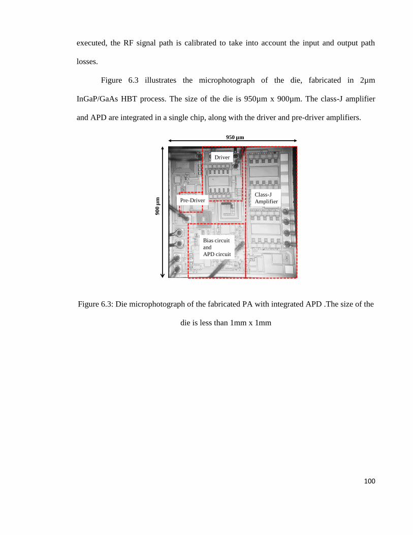
100
executed, the RF signal path is calibrated to take into account the input and output path
losses.
Figure 6.3 illustrates the microphotograph of the die, fabricated in 2µm
InGaP/GaAs HBT process. The size of the die is 950µm x 900µm. The class-J amplifier
and APD are integrated in a single chip, along with the driver and pre-driver amplifiers.
950 µm
90
0 µ
m
Class-J
Amplifier
Driver
Pre-Driver
Bias circuit
and
APD circuit
Figure 6.3: Die microphotograph of the fabricated PA with integrated APD .The size of the
die is less than 1mm x 1mm
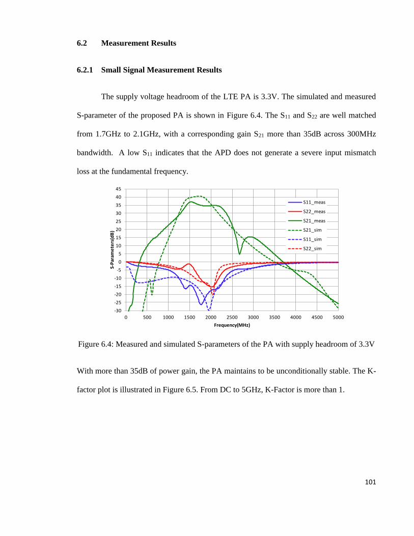
101
6.2 Measurement Results
6.2.1 Small Signal Measurement Results
The supply voltage headroom of the LTE PA is 3.3V. The simulated and measured
S-parameter of the proposed PA is shown in Figure 6.4. The S11 and S22 are well matched
from 1.7GHz to 2.1GHz, with a corresponding gain S21 more than 35dB across 300MHz
bandwidth. A low S11 indicates that the APD does not generate a severe input mismatch
loss at the fundamental frequency.
-30
-25
-20
-15
-10
-5
0
5
10
15
20
25
30
35
40
45
0 500 1000 1500 2000 2500 3000 3500 4000 4500 5000
S-P
aram
ete
rs(d
B)
Frequency(MHz)
S11_meas
S22_meas
S21_meas
S21_sim
S11_sim
S22_sim
Figure 6.4: Measured and simulated S-parameters of the PA with supply headroom of 3.3V
With more than 35dB of power gain, the PA maintains to be unconditionally stable. The K-
factor plot is illustrated in Figure 6.5. From DC to 5GHz, K-Factor is more than 1.
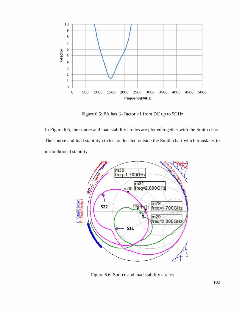
102
0
1
2
3
4
5
6
7
8
9
10
0 500 1000 1500 2000 2500 3000 3500 4000 4500 5000
K-F
acto
r
Frequency(MHz)
Figure 6.5: PA has K-Factor >1 from DC up to 5GHz
In Figure 6.6, the source and load stability circles are plotted together with the Smith chart.
The source and load stability circles are located outside the Smith chart which translates to
unconditional stability.
S22
S11
Figure 6.6: Source and load stability circles
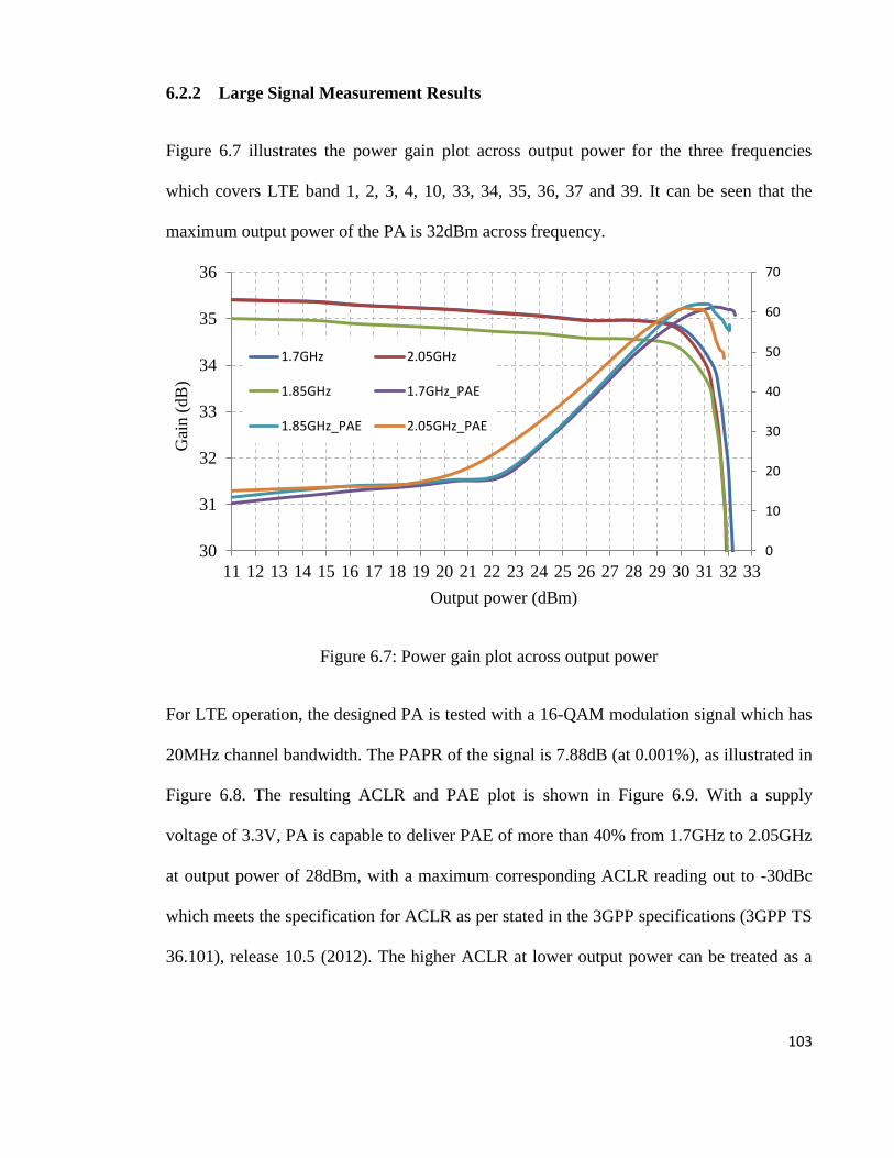
103
6.2.2 Large Signal Measurement Results
Figure 6.7 illustrates the power gain plot across output power for the three frequencies
which covers LTE band 1, 2, 3, 4, 10, 33, 34, 35, 36, 37 and 39. It can be seen that the
maximum output power of the PA is 32dBm across frequency.
0
10
20
30
40
50
60
70
30
31
32
33
34
35
36
11 12 13 14 15 16 17 18 19 20 21 22 23 24 25 26 27 28 29 30 31 32 33
Gai
n (
dB
)
Output power (dBm)
1.7GHz 2.05GHz
1.85GHz 1.7GHz_PAE
1.85GHz_PAE 2.05GHz_PAE
Figure 6.7: Power gain plot across output power
For LTE operation, the designed PA is tested with a 16-QAM modulation signal which has
20MHz channel bandwidth. The PAPR of the signal is 7.88dB (at 0.001%), as illustrated in
Figure 6.8. The resulting ACLR and PAE plot is shown in Figure 6.9. With a supply
voltage of 3.3V, PA is capable to deliver PAE of more than 40% from 1.7GHz to 2.05GHz
at output power of 28dBm, with a maximum corresponding ACLR reading out to -30dBc
which meets the specification for ACLR as per stated in the 3GPP specifications (3GPP TS
36.101), release 10.5 (2012). The higher ACLR at lower output power can be treated as a
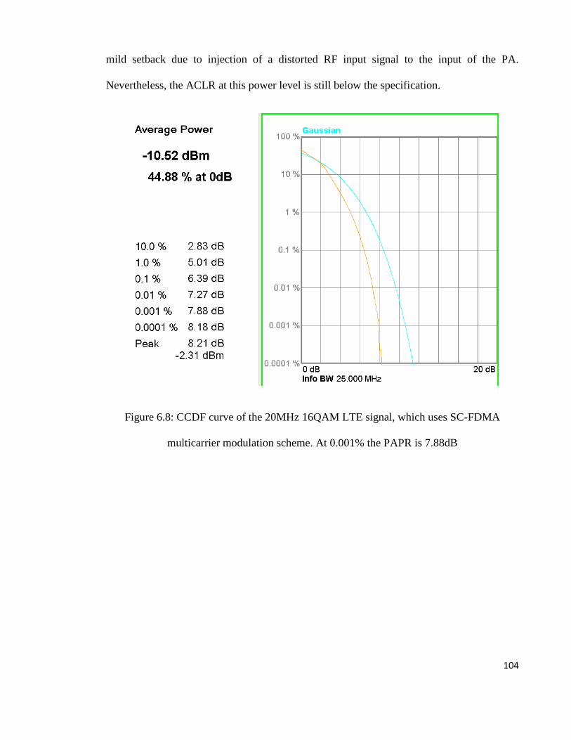
104
mild setback due to injection of a distorted RF input signal to the input of the PA.
Nevertheless, the ACLR at this power level is still below the specification.
Figure 6.8: CCDF curve of the 20MHz 16QAM LTE signal, which uses SC-FDMA
multicarrier modulation scheme. At 0.001% the PAPR is 7.88dB
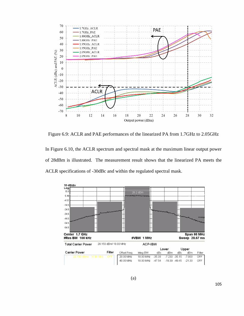
105
Figure 6.9: ACLR and PAE performances of the linearized PA from 1.7GHz to 2.05GHz
In Figure 6.10, the ACLR spectrum and spectral mask at the maximum linear output power
of 28dBm is illustrated. The measurement result shows that the linearized PA meets the
ACLR specifications of -30dBc and within the regulated spectral mask.
(a)
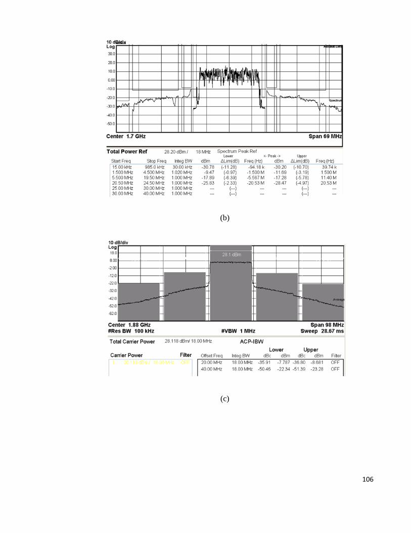
106
(b)
(c)
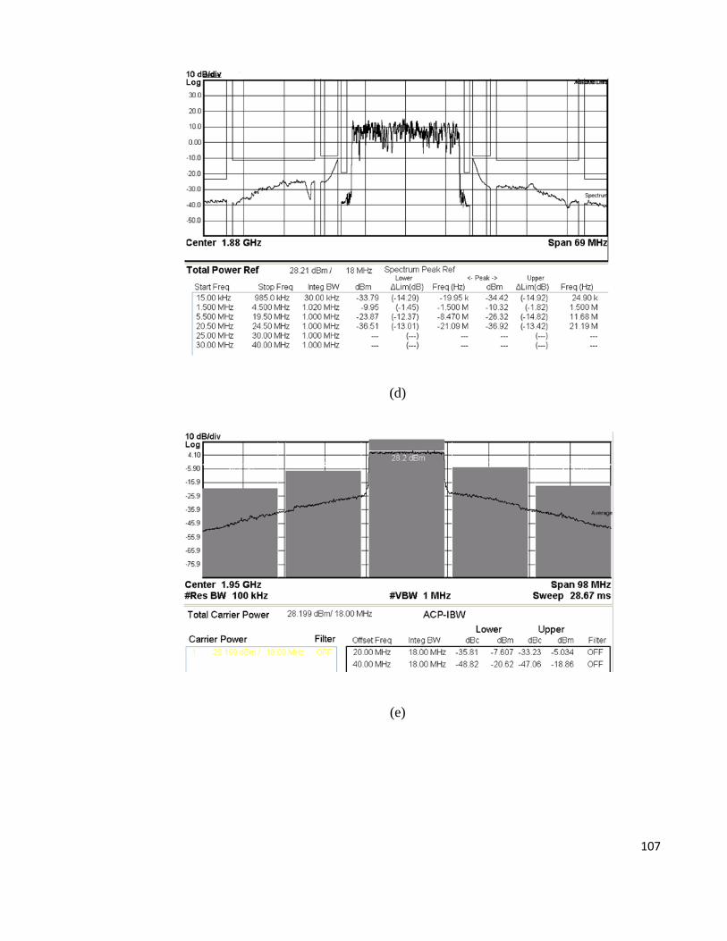
107
(d)
(e)
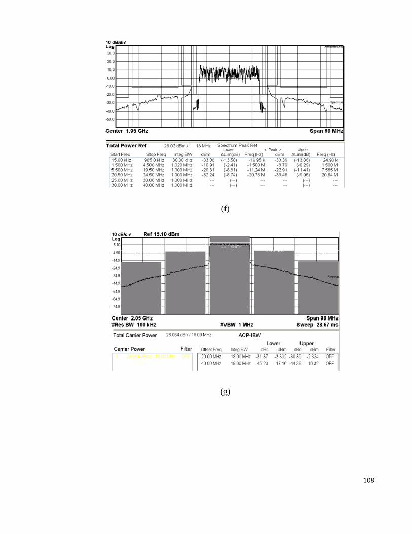
108
(f)
(g)
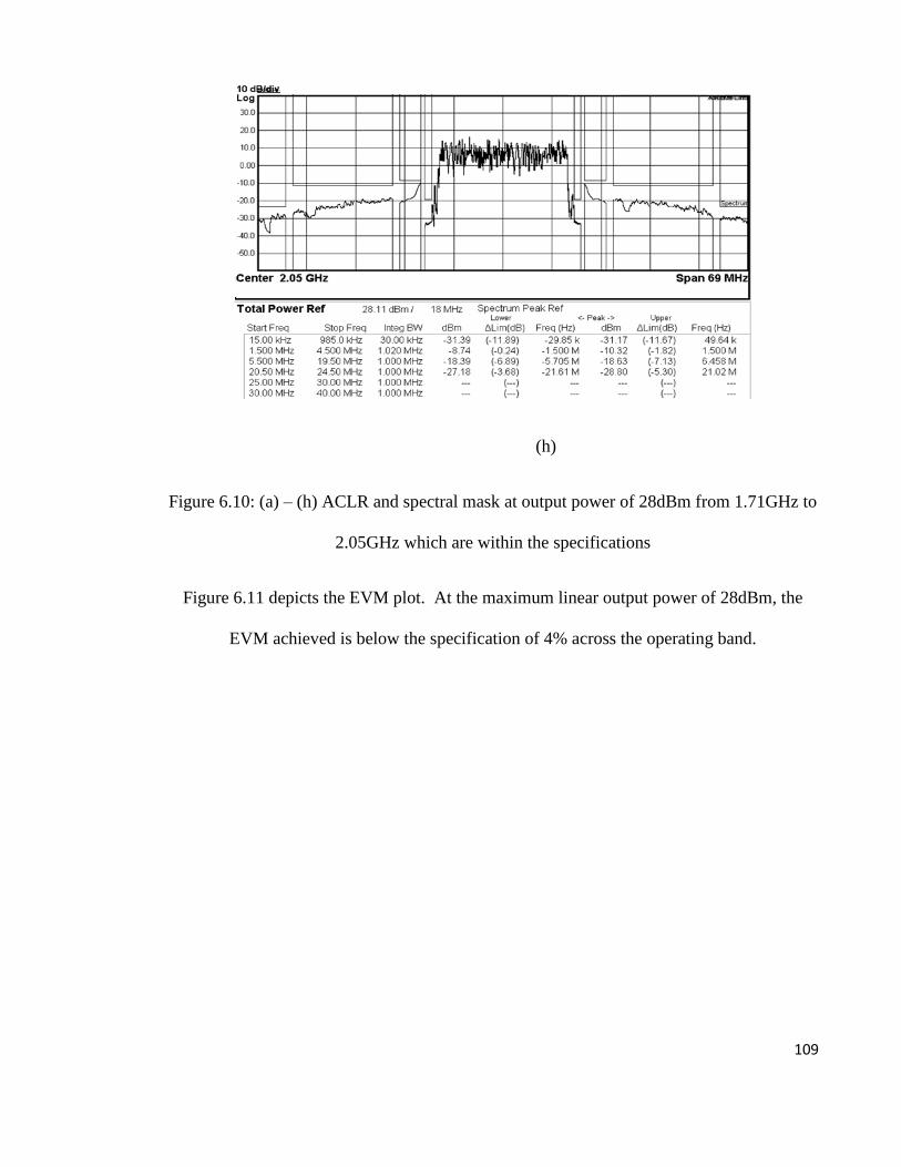
109
(h)
Figure 6.10: (a) – (h) ACLR and spectral mask at output power of 28dBm from 1.71GHz to
2.05GHz which are within the specifications
Figure 6.11 depicts the EVM plot. At the maximum linear output power of 28dBm, the
EVM achieved is below the specification of 4% across the operating band.
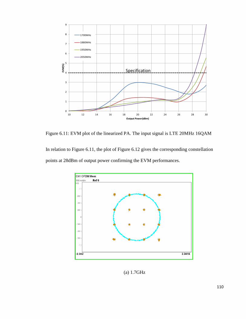
110
0
1
2
3
4
5
6
7
8
9
10 12 14 16 18 20 22 24 26 28 30
EVM
(%)
Output Power(dBm)
1700MHz
1880MHz
1950MHz
2050MHz
Specification
Figure 6.11: EVM plot of the linearized PA. The input signal is LTE 20MHz 16QAM
In relation to Figure 6.11, the plot of Figure 6.12 gives the corresponding constellation
points at 28dBm of output power confirming the EVM performances.
(a) 1.7GHz
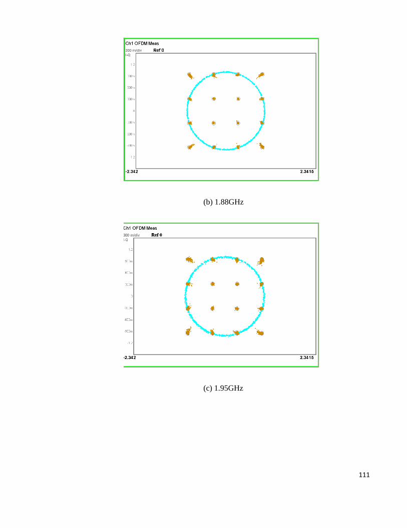
111
(b) 1.88GHz
(c) 1.95GHz
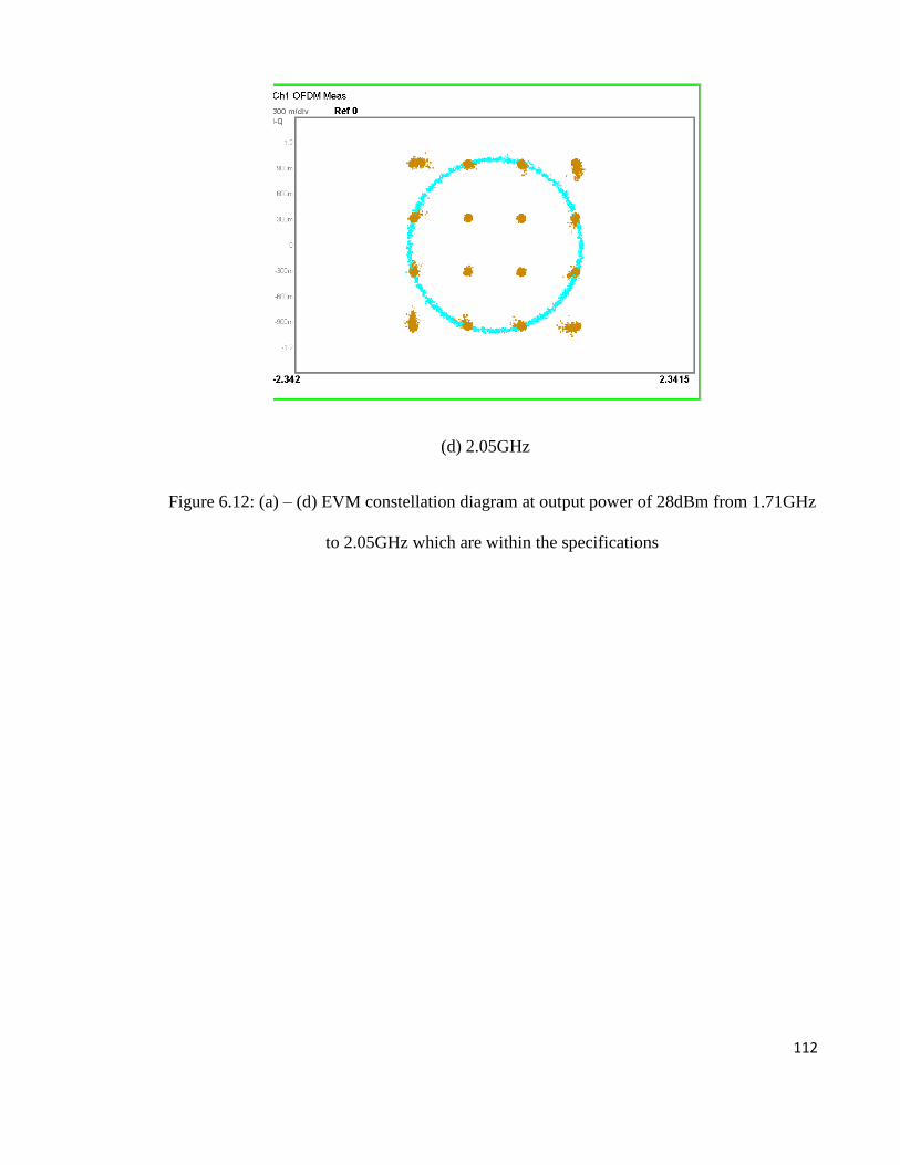
112
(d) 2.05GHz
Figure 6.12: (a) – (d) EVM constellation diagram at output power of 28dBm from 1.71GHz
to 2.05GHz which are within the specifications
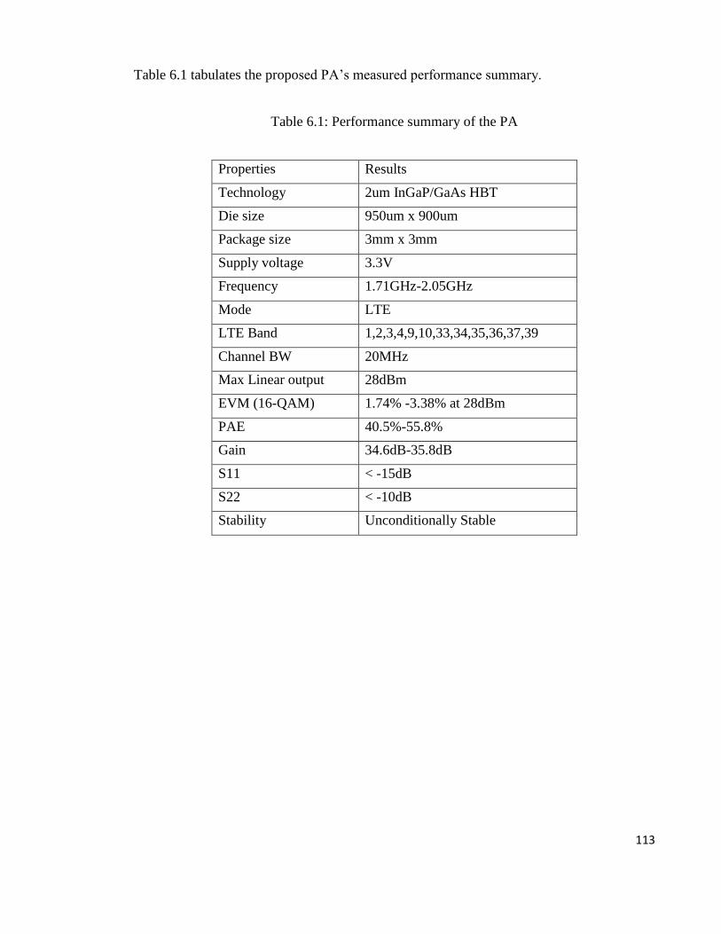
113
Table 6.1 tabulates the proposed PA’s measured performance summary.
Table 6.1: Performance summary of the PA
Properties Results
Technology 2um InGaP/GaAs HBT
Die size 950um x 900um
Package size 3mm x 3mm
Supply voltage 3.3V
Frequency 1.71GHz-2.05GHz
Mode LTE
LTE Band 1,2,3,4,9,10,33,34,35,36,37,39
Channel BW 20MHz
Max Linear output
Power
28dBm
EVM (16-QAM) 1.74% -3.38% at 28dBm
PAE 40.5%-55.8%
Gain 34.6dB-35.8dB
S11 < -15dB
S22 < -10dB
Stability Unconditionally Stable
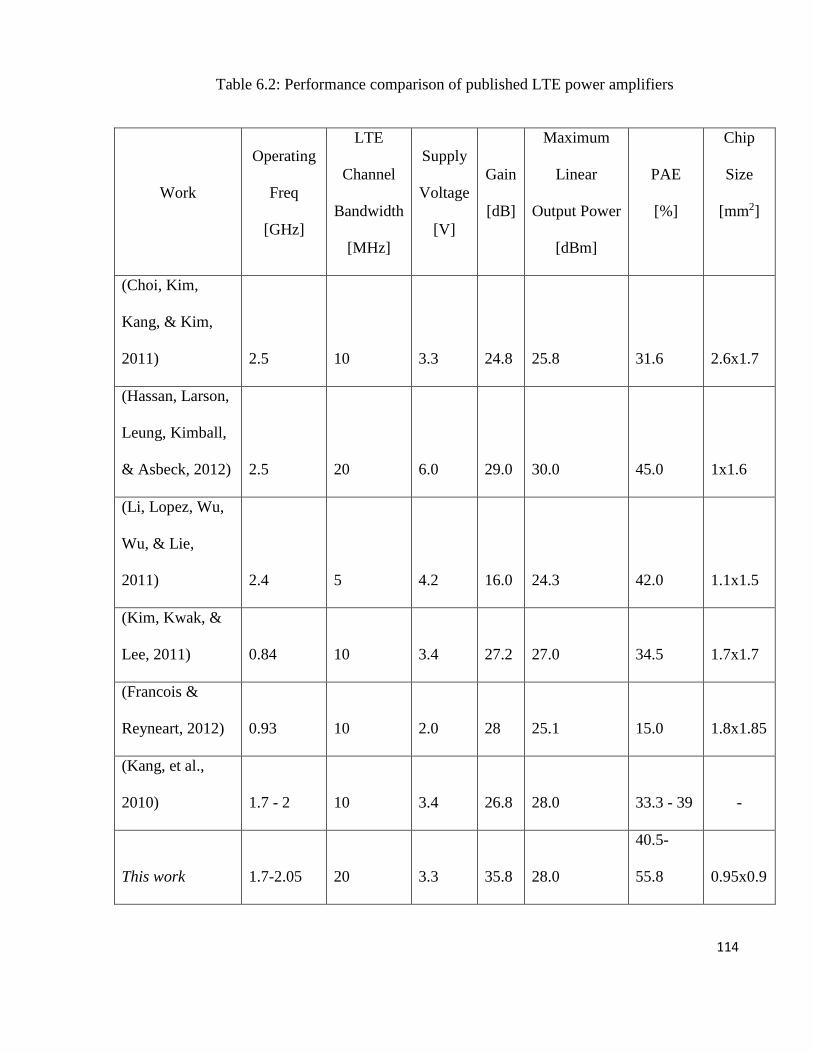
114
Table 6.2: Performance comparison of published LTE power amplifiers
Work
Operating
Freq
[GHz]
LTE
Channel
Bandwidth
[MHz]
Supply
Voltage
[V]
Gain
[dB]
Maximum
Linear
Output Power
[dBm]
PAE
[%]
Chip
Size
[mm2]
(Choi, Kim,
Kang, & Kim,
2011) 2.5 10 3.3 24.8 25.8 31.6
2.6x1.7
(Hassan, Larson,
Leung, Kimball,
& Asbeck, 2012) 2.5 20 6.0 29.0 30.0 45.0
1x1.6
(Li, Lopez, Wu,
Wu, & Lie,
2011) 2.4 5 4.2 16.0 24.3 42.0
1.1x1.5
(Kim, Kwak, &
Lee, 2011) 0.84 10 3.4 27.2 27.0 34.5
1.7x1.7
(Francois &
Reyneart, 2012) 0.93 10 2.0 28 25.1 15.0
1.8x1.85
(Kang, et al.,
2010) 1.7 - 2 10 3.4 26.8 28.0 33.3 - 39
-
This work 1.7-2.05 20 3.3 35.8 28.0
40.5-
55.8
0.95x0.9
115
In Table 6.2, recent work on envelope tracking methodology by (Hassan, Larson,
Leung, Kimball, & Asbeck, 2012) and (Kang, et al., 2010) indeed has improve the PAE of
the LTE PA. Furthermore, (Kang, et al., 2010) has achieved more than 30% PAE for
300MHz bandwidth. Both technique needs the additional CMOS chip besides the GaAs
HBT PA to achieve the reported performance. An attempt by (Francois & Reyneart, 2012)
is a great start to design LTE PA with CMOS process. However, work still need to be done
to improve the PAE.
On the other hand, the proposed architecture in this research able to deliver more
than 40% PAE for bandwidth of 350MHz. This is achieved with integrating a wideband
efficiency PA (Class-J) and the linearization scheme (APD) in a single chip. Furthermore,
the performance is achieved with high gain of more than 34dB for 350MHz bandwidth.
The comparison data shows that the designed architecture can be well implemented in the
handset’s transmitter without much constraint in terms of performance and space on the
phone board.

116
CHAPTER 7. CONCLUSION AND FUTURE WORKS
7.1 Conclusion
In this work, the design of a multi-band LTE power amplifier has been presented.
The design integrates two distinct techniques which are the class-J power amplifier to
improve backed-off output power efficiency and analog pre-distorter linearization scheme
which ensure PA meets the linear transmission specifications respectively.
In order to meet the wideband performance, the design of a power cell is
highlighted in Chapter 3. The optimum power cell size followed by the integrating
ballasting concept is proven essential through this chapter. As a result, a novel ballasting
concept which does not serve a trade-off for linearity and efficiency is successfully
designed and implemented. In a nutshell, the foundation of the power amplifier building is
strengthen before moving to the next level. Also, importance is given in choosing an
optimum conduction angle for the power amplifier. Through Fourier analysis, an optimum
operating point in the appreciation of the linearity and efficiency is defined. This operating
point was verified through bias sweep experiment analysis. On the other hand, an
appropriate biasing circuit to bias up the respective power cells has been reviewed in. The
biasing circuits is constructed in an effort to make sure it does not impact the linearity of
the PA.
Chapter 4 demonstrates the design methodology of class-J power amplifier. The
mathematical analysis concludes the need of a reactive second harmonic termination to
amend the voltage component of the PA to boost up its efficiency. Load pull simulation is
117
executed in order to determine the optimum fundamental and second harmonic output
impedances. This is followed by the design of the desired output matching network which
delivers more than 40% power added efficiency from 1.7GHz to 2.0GHz at backed off
output power of 28dBm. The highest efficiency is at 2.05GHz which reads to 55.8%.
In Chapter 5, a novel analog pre-distorter linearization scheme is designed to meet
the linearity specification from 1.7GHz to 2.05GHz. The insight of this design is to execute
the amplitude and phase linearization through two sub-circuits which ensures wideband
operation. Furthermore, these circuits are implemented as an integrating part of the PA
itself.
The designed PA consists of a 950µm x 900µm die mounted on a 3mm x 3mm
package is capable to operate linearly from 1.7GHz to 2.05GHz which covers LTE band
1,2,3,4,9,10,33,34,35,36,37 and 39. The PAE ranges from 40.5% to 55.8%. The size and
performance of the PA places it as the right choice for handset applications.

118
7.2 Future Works
The successful implementation of the class-J power amplifier with integrated analog pre-
distorter linearizer in this work increases the desire to further improve the linearity and
efficiency to cater for the increasing data rate requirement. This opens the door for future
works. The suggestions are as follows:
a) Improve the efficiency of the APD linearized class-J PA with integrated envelope
tracking method.
b) Improving the linearity of the wideband efficiency class-J PA with digital pre-
distortion linearization (DPD). Through this method, the class-J PA can be used for
base station application which has more stringent linearity specifications.
c) Integrating the APD linearization technique with other high efficiency topology
such as Doherty power amplifier.
d) To explore all the above mentioned techniques with CMOS process which will
benefit in the context of cost.
119
REFERENCES
3GPP TS 36.101 version 9.4.0 Release 9. (2010). Retrieved from ETSI: http://www.etsi.org
Akter, R., Islam, M.-R., & Song, J.-B. (2010). PAPR in 3rd Generation Partnership Project
Long Term Evolution: An Overview to Find the Impact. IETE Technical Review,
493-502.
Amon, C. (4 March, 2011). LTE: The Road Ahead. EE Times.
Aref, A.-F., Askar, A., Nafe, A., Tarar, M., & Negra, R. (2012). Efficient Amplification of
Signals with High PAPR using a Novel Multilevel LINC Transmitter Architecture.
7th European Microwave Integrated Circuit Conference (pp. 655-658). Amsterdam:
IEEE.
Bahl, I. (2003). Lumped Elements for RF and Microwave Circuits. Norwood: Artech
House.
Bahl, I. (2009). Fundamentals of RF and Microwave Transistor Amplifiers. New Jersey:
Wiley.
Bayraktaroglu, B., & Salib, M. (1997). Unconditional Thermally Stable Cascode GaAs
HBTs for Microwave Applications. IEEE Microwave Guided Wave Letters, 187-
189.
Bulja, S., & Syahkal, D.-M. (2009). Combined Low Frequency and Third Harmonic
Injection in Power Amplifier Linearization. IEEE Microwave and Wireless
Components Letters, 584-586.
Carvalho, N., & Pedro, C. (1999). Gain Compression or Expansion, Distortion and Other
Large Signal Power Amplifier Related Phenomena. Telecommunication Conference
(pp. 1-4). Sesembra: University De Aveiro.
Carvalho, N., & Pedro, J.-C. (1999). Compact Formulas to Relate ACPR and NPR to Two
Tone IMR and IP3. Microwave Journal, 70-75.
Cha, J., Yi, J., Kim, J., & Kim, B. (2004). Optimum Design of a Predistortion RF Power
Amplifier for Multicarrier WCDMA Applications. IEEE Transactions on
Microwave Theory and Techniques, 655-663.
120
Chen, C.-T., Li, C.-J., Horng, T.-S., Jau, J.-K., & Li, J.-Y. (2009). Design and Linearization
of Class-E Power Amplifier for Nonconstant Envelope Modulation. IEEE
Transaction on Microwave Theory and Techniques, 957-964.
Cho, Y., Kang, D., Kim, J., Kim, D., Park, B., & Kim, B. (2013). A Dual Power Mode
Multi-band Power Amplifier with Envelope Tracking for Handset Applications.
IEEE Transactions on Microwave Theory and Techniques, 1608-1619.
Choi, J., Kim, D., Kang, D., & Kim, B. (2009). A Polar Transmitter with CMOS
Programmable Hysteretic Controlled Hybrid Switching Supply Modulator for
Multi-Standard Applications. IEEE Transactions on Microwave Theory and
Techniques, 1675-1686.
Choi, J., Kim, D., Kang, D., & Kim, B. (2011). A New Power Management IC Architecture
for Envelope Tracking Power Amplifier. IEEE Transactions on Microwave Theory
and Techniques, 1796-1802.
Chu, W., Bakkaloglu, B., & Kiaei, S. (2008). A 10MHz Bandwidth 2mV-Ripple PA-
Supply Regulator for CDMA Transmitters. IEEE International Solid Circuit
Conference Digest Technical Papers, 448-449.
Colantonio, P., Giannini, F., & Limiti, E. (2009). High Efficiency RF and Microwave Solid
State Power Amplifiers. West Sussex: John Wiley.
Cripps, S. (2006). Advanced RF Power Amplifier Techniques for Modern Wireless and
Microwave Systems. Chard: Hywave Associates.
Cripps, S. (2006). RF Power Amplifiers for Wireless Communications. Norwood: Artech
House.
Cripps, S. (2012). Amplifier Classes, A to S. In J. Walker, Handbook of RF and Microwave
Power Amplifiers (pp. 159-161). Cambridge: Cambridge University Press.
Deng, J., Gudem, P.-S., Larson, L.-E., & Asbeck, P.-M. (2005). A High Average Efficiency
SiGe HBT Power Amplifier for WCDMA Handset Applications. IEEE
Transactions on Microwave Theory and Techniques, 529-537.
Deng, J., Gudem, P.-S., Larson, L.-E., Kimball, D.-F., & Asbeck, P.-M. (2006). A SiGe PA
with Dual Dynamic Bias Control and Memoryless Digital Predistortion for
WCDMA Handset Applications. IEEE Journal of Solid State Circuits, 1210-1221.
121
Doherty, W.-H. (1936). A New High Efficiency Power Amplifier for Modulated Waves.
Bell System Technical Journal,The, 469-475.
Dong, Y., Zhang, W.-R., Jun, Q.-J., Pan, G., & Ying, X. (2006). A Simple Method to
Optimize the Ballasting Resistor of RF Power HBT. IEEE International Symposium
on Antenna Propagation and EM Theory (pp. 1-4). Guilin: IEEE.
Francois, B., & Reyneart, P. (2012). A Fully Integrated Watt Level Linear 900MHZ CMOS
RF Power Amplifier for LTE Applications. IEEE Transactions on Microwave
Theory and Techniques, 1878-1885.
Ganesan, S. (1993). GaAs/AlGaAs HBT Device Modeling and Implementation as a High
Power Device in Broadband Microwave Circuits. Ohio: Ohio University.
Gilmore, R., & Besser, L. (2003). Practical RF Circuit Design for Modern Wireless
Systems. Norwood: Artech House.
Gonzalez, G. (1997). Microwave Transistor Amplifiers. New Jersey: Prentice Hall.
Gray, P., Hurst, P., Lewis, S., & Meyer, R. (2005). Analysis and Design of Analog
Integrated Circuits. New York: Wiley.
Han, K., & Kim, B. (2008). A Parallel Power Amplifier with a Novel Mode Switching
Control. IEEE Microwave and Wireless Components Letters, 200-202.
Hassan, M., Larson, L.-E., Leung, V.-W., Kimball, D.-F., & Asbeck, P.-M. (2012). A
Wideband CMOS/GaAs HBT Envelope Tracking Power Amplifier for 4G LTE
Mobile Terminal Applications. IEEE Transactions on Microwave Theory and
Techniques, 1321-1330.
Hau, G., Nishimura, T.-B., & Iwata, N. (2001). A Highly Efficient Linearized Wide-Band
CDMA Handset Power Amplifier based on Predistortion Under Various Bias
Conditions. IEEE Transactions on Microwave Theory and Techniques, 1194-1201.
Heinrich, W., Wentzel, A., & Melaini, C. (2010). Advanced Switch-Mode Concepts using
GAN: The Class-S Amplifier. Microwave Radar and Wireless Communications
(MIKON) (pp. 1-6). Lithuania: IEEE.
Huang, J., Liao, Y., & Chen, Z. (2010). A dual mode GaAs HBT Power Amplifier for LTE
Applications. IEEE International Conference on Solid State and Integrated Circuit
Technology Proceedings (pp. 722-724). Shanghai: IEEE.

122
Iwamoto, M., Williams, A., Chen, P.-F., Metzger, A.-G., Larson, L.-E., & Asbeck, P.
(2001). An Extended Doherty Amplifier with High Efficiency Over A Wide Power
Range. IEEE Transactions on Microwave Theory and Techniques, 2472-2479.
Jang, J., Kan, E., Arnborg, T., Johansson, T., & Dutton, R. (1998). Characterization of RF
Power BJT and Improvement of Thermal Stability with Nonlinear Base Ballasting.
IEEE Solid State Circuit Journal, 1428-1432.
Jeong, J., Kimball, D.-F., Kwak, M., Hsia, C., Draxler, P., & Asbeck, P.-M. (2009).
Wideband Envelope Tracking Power Amplifiers with Reduced Bandwidth Power
Supply Waveforms and Adaptive Digital Predistortion Techniques. IEEE
Transactions on Microwave Theory and Techniques, 3307-3314.
Kahn, L.-R. (1952). Single Sideband Transmission by Envelope Elimination and
Restoration. IRE Proceedings, 803-806.
Kang, D., Choi, J., Yu, K., Min, K., Min, M., Jun, M., . . . Kim, B. (2009). Input Power
Dividing of Doherty Power Amplifiers for Handset Applications. IEEE MTT-S
International Microwave Symposium (pp. 421-424). Boston: IEEE.
Kang, D., Kim, D., Cho, Y., Park, B., Kim, J., & Kim, B. (2011). Design of Bandwidth
Enhanced Doherty Power Amplifiers for Handset Applications. IEEE Transactions
on Microwave Theory and Techniques, 3474-3483.
Kang, D., Kim, D., Choi, J., Kim, J., Cho, Y., & Kim, B. (2010). A Multimode/Multiband
Power Amplifier with a Boosted Supply Modulator for Multi-Standard
Applications. IEEE Transactions on Microwave Theory and Techniques, 2598-
2608.
Kang, D., Yu, D., Min, K., Choi, J., Jun, M., Kim, D., & Kim, B. (2008). Class-AB/F
Doherty Power Amplifiers. Proceedings of 38th European Microwave Conference
(pp. 230-233). Amsterdam: IEEE.
Kang, D., Yu, D., Min, K., Han, K., Choi, J., Kim, D., . . . Kim, B. (2008). A Highly
Efficient and Linear Class-AB/F Power Amplifier for Multimode Operation. IEEE
Transactions on Microwave Theory and Techniques, 77-87.
Kang, S., Park, U., Lee, K., & Hong, S. (2003). Adaptive Feedforward Amplifier using
Digital Contoller. 57th IEEE Semianual Vehicular Technology Conference (pp.
2076-2079). South Korea: IEEE.

123
Kato, T., Yamaguchi, K., & Kuriyama, Y. (2006). A Doherty Power Amplifier Module for
Mobile Terminals with Variable Linearity Function. Proceedings of Asia-Pacific
Microwave Conference (pp. 1881-1884). Yokohama: IEEE.
Katz, A. (2001). Linearization: Reducing Distortion in Power Amplifiers. IEEE Microwave
Magazine, 37-49.
Kim, B., Kwak, C., & Lee, J. (2011). A Dual Mode Power Amplifier with on Chip Switch
Bias Control Circuits for LTE Handsets. IEEE Transactions on Circuits and
Systems, 857-861.
Kim, B., Kwak, C., & Lee, J. (2011). A Dual Mode Power Amplifier with on Chip Switch
Bias Control Circuits for LTE Handsets. IEEE Transactions on Circuits and
Systems, 857-861.
Kim, I., Cha, J., Hong, S., Woo, Y., Kim, J., & Kim, B. (2006). Predistortion Power
Amplifier for Base Station using a Feedforward Loop Linearizer. 36th European
Microwave Conference (pp. 141-144). Manchester: IEEE.
Kim, J., Son, S., Jee, S., Kim, S., & Kim, B. (2013). Optimization of Envelope Tracking
Power Amplifier for Base Station Applications. IEEE Transactions on Microwave
Theory and Techniques, 1620-1627.
Kim, W., Kang, S., Lee, K., Chung, M., & Kang, J. (2002). Analysis of Nonlinear Behavior
of Powr HBTs. IEEE Transactions on Microwave Theory and Techniques, 1714-
1722.
Kousai, S., Onikuza, K., Yamaguchi, T., Kuriyama, Y., & Nagaoka, M. (2012). A 28.3mW
PA Closed Loop for Linearity and Efficiency Improvement Integrated in a
27.12dBm WCDMA CMOS Power Amplifier. IEEE International Solid State
Circuits Conference Digest Technical Papers, 84-86.
Landin, P.-N., Fritzin, J., Moer, W.-V., Isaksson, M., & Alvanpour, A. (2012). Modeling
and Digital Predistortion of Class D Outphasing RF Power Amplifiers. IEEE
Transactions on Microwave Theory and Techniques, 1907-1915.
Legarda, J., Presa, J., E, H., Solar, H., J, M., & J, P. (2005). An Adaptive Feedforward
Amplifier under Maximum Output Control Method for UMTS Downlink
Transmitters. IEEE Transactions on Microwave Theory and Techniques, 2481-
2486.

124
Li, Y., Lopez, J., Wu, P.-H. H., Wu, R., & Lie, D.-Y. (2011). A SiGe Envelope Tracking
Power Amplifier with an Integrated CMOS Envelope Modulator for Mobile
WiMAX/3GPP LTE Transmitters. IEEE Transactions on Microwave Theory and
Techniques, 2525-2536.
Liou, J.-J., Liou, L.-L., & Huang, C.-I. (1994). Analytical Model for the AlGaAs/GaAs
Multiemitter Finger HBT Including Self Heating and Thermal Coupling Effects.
IET Journal, 469-475.
Liou, L.-L., Jenkins, T., & Huang, C.-I. (1996). Effect of Base Potential Distribution on
Thermal Runaway and the Power Limitation of the Heterojunction Bipolar
Transistor with CIrcular Dot Geometry. Electron Devices Meeting (pp. 49-52).
Ohio: IEEE.
Liu, W., Khatibzadeh, A., Sweder, J., & Chau, H.-F. (1996). The Use of Base Ballasting to
Prevent the Collapse of Current Gain in AlGaAs/GaAs Heterojunction Bipolar
Transistors. IEEE Electron Devices, 245-251.
Liu, W., Nelson, S., Hill, D.-G., & Khatibzadeh, A. (1993). Current Gain Collapse in
Microwave Multifinger Heterojunction Bipolar Transistors Operated at very High
Power Densities. IEEE Electron Device, 1917-1927.
Ludwig, R., & Bretchko, P. (2000). RF Circuit Design Theory and Applications. New
Jersey: Prentice Hall.
Maas, S. (2006). Ballasting HBTs for Wireless Power Amplifier Operation. ARMMS
Conference (pp. 1-9). Steventon: ARMMS UK.
Maier, S., Wiegner, D., Zierdt, M., Kuebart, W., Seyfried, U., Haslach, C., . . . Quay, R.
(2011). 900 MHz Pulse Width Modulated Class-S Power Amplifier with Improved
Linearity. Microwave Symposium Digest (MTT) (pp. 1-4). Baltimore: IEEE.
Moon, J., Kim, J., & Kim, B. (2010). Investigation of a Class-J Power Amplifier with a
Non-linear Cout for Optimized Operation. IEEE Transactions on Microwave
Theory and Techniques, 2800-2811.
Moon, J., Son, J., Lee, J., & Kim, B. (2011). A Multimode/Multiband Envelope Tracking
Transmitter with Broadband Saturated Amplifier. IEEE Transactions on Microwave
Theory and Techniques, 3463-3473.
125
Nam, J., & Kim, B. (2007). The Doherty Power Amplifier with On-Chip Dynamic Bias
Control Circuit for Handset Application. IEEE Transactions on Microwave Theory
and Techniques, 633-642.
Park, H.-M., Baek, D.-H. J.-I., & Hong, S. (2000). A Predistortion Linearizer Using
Envelope Feedback Technique with Simplified Carrier Cancellation Scheme for
Class-A and Class-AB Power Amplifiers. IEEE Transactions on Microwave Theory
and Techniques, 898-904.
Pinon, V., Hasbani, F., Giry, A., Pache, D., & Garnier, C. (2008). A Single Chip WCDMA
Envelope Reconstruction LDMOS PA with 130MHz Switched Mode Power
Supply. IEEE International Solid State Circuits Conference Digest Technical
Papers, 564-565.
Pozar, D. (2005). Microwave Engineering. New York: Wiley.
Raab, F.-H., Asbeck, P., Cripps, S., Kenington, P.-B., Popovic, Z.-B., Pothecary, N., . . .
Sokal, N.-O. (2002). Power Amplifiers and Transmitters for RF and Microwave.
IEEE Transactions on Microwave Theory and Techniques, 814-826.
Rana, M.-M., Islam, M.-S., & Kouzani, A.-Z. (2010). Peak to Average Power Ratio
Analysis for LTE Systems. IEEE International Conference on Communication
Software and Networks (pp. 516-520). Singapore: IEEE.
Reynaert, P., & Steyaert, M. (2005). A 1.7GHz Polar Modulated CMOS RF Power
Amplifier for GSM-EDGE. IEEE Journal of Solid State Circuits, 2598-2608.
Rollett, J.-M. (1962). Stability and Power Gain Invariants of Linear Two Ports. IRE
Transactions on Circuit Theory, 29-32.
Rui, M., Zhancang, W., Yang, X., & Lanfranco, S. (2012). Implementation of a Current
Mode Class-S RF Power Amplifier with GaN HEMTS for LTE Advanced. Wireless
and Microwave Technology Conference (WAMICON) (pp. 1-6). Florida: IEEE.
Rumney, M. (2009). Air Interface Concepts. In M. Rumney, LTE and the Evolution to 4G
Wireless (pp. 11-57). China: Agilent Technologies.
Rumney, M. (2009). LTE and the Evolution to 4G Wireless. China: Agilent Technologies.
Rumney, M. (2009). LTE Introduction. In M. Rumney, LTE and the Evolution to 4G
Wireless (pp. 1-7). China: Agilent Technologies.
126
Sahu, B., & Rincon-Mora, G.-A. (2007). A High Efficiency WCDMA RF Power Amplifier
with Adaptive Dual Mode Buck-Boost Supply and Bias Current Control. IEEE
Microwave and Wireless Components Letters, 238-240.
Shameli, A., Safarian, A., Rofougaran, A., Rofougaran, M., & DeFlaviis, F. (2008). A Two
Point Modulation Technique for CMOS Power Amplifier in Polar Transmitter
Architecture. IEEE Transactions on Microwave Theory and Techniques, 31-38.
Suzuki, Y., Ohkawara, J., & Narahashi, S. (2011). A 3.5GHz Band 140-W Class Wideband
Feedforward Power Amplifier for Mobile Base Stations. General Assembly and
Scientific Symposium (pp. 1-4). Istanbul: IEEE.
Suzuki, Y., Ohkawara, J., & Narahashi, S. (2011). A 3.5GHz Band 140-W Class Wideband
Feedforward Power Amplifier for Mobile Base Stations. General Assembly and
Scientific Symposium (pp. 1-4). Istanbul: IEEE.
Sweet, A. (1990). MIC and MMIC Amplifier and Oscillator Circuit Design. Norwood:
Artech House.
Sweet, A. (2008). Designing Bipolar Transistor Radio Frequency Integrated Circuits.
Norwood: Artech House.
Takahashi, K., Yamanouchi, Y., Hirayama, & Kunihiro, k. (2008). An Envelope Tracking
power Amplifier Using an Adaptive Biased Envelope Amplifier for WCDMA
Handsets. Radio Frequency Integrated Circuits (RFIC) Symposium (pp. 405-408).
Atlanta: IEEE.
Thein, T.-T., Law, C.-L., & Fu, K. (2011). Frequency Domain Dynamic Thermal Analysis
in GaAs HBT for Power Amplifier Applications. Progress in Electromagnetic
Research, 71-87.
Tombak, A., Baeten, R.-J., Jorgenson, J.-D., & Dening, D.-C. (2006). Integration of a
Cellular Handset Power Amplifier and a DC/DC Converter in a Silicon-On-
Insulator(SOI) Technology. Radio Frequency Integrated Circuits (RFIC)
Symposium (pp. 413-416). Atlanta: IEEE.
Tuffery, A., Deltimple, N., Leite, B., Cathelin, P., Knopik, V., & Kerherye, E. (2011). A
27.5dBm Linear Reconfigurable CMOS Power Amplifier for 3GPP LTE
Applications. NEWCAS (pp. 221-224). France: IEEE.
Tuffy, T., Zhu, A., & Brazil, T.-J. (2011). Class-J RF Power Amplifier with Wideband
Harmonic Supression. IEEE MTT-S International (pp. 1-4). Baltimore: IEEE.

127
Walsh, K., & Johnson, J. (2009). 3G/4G Multimode Cellular Front End Challenges; Impact
on Power Amplifier Design. San Jose: RFMD.
Wang, F., Kimball, D.-F., Lie, D.-Y., & Asbeck, P.-M. L.-E. (2007). A Monolithic High
Efficiency 2.4GHz 20-dBm SiGe BiCMOS Envelope Tracking OFDM Power
Amplifier. IEEE Journal of Solid State Circuits, 1271-1281.
Wen, J.-C., & Sun, L.-L. (2006). A GaAs HBT Power Amplifier with a Newly Active Bias
Linearizer for WCDMA Terminal. 8th International Conference on Solid State and
Integrated Circuit Technology Proceedings (pp. 1727-1729). Shanghai: IEEE.
Wentzel, A., Meliani, C., & Heinrich, W. (2010). RF Class-S Power Amplifiers: State of
the Art Results and Potential. Microwave Symposium Digest (MTT) (pp. 812-815).
Anaheim: IEEE.
Wright, P., Lees, J., Benedikt, J., Tasker, P.-J., & Cripps, S.-C. (2009). A Methodology for
Realizing High Efficiency Class-J in Linear and Broadband Power Amplifier. IEEE
Transactions on Microwave Theory and Techniques, 3196-3204.
Yamanouchi, S., Aoki, Y., Kunihiro, K., Hirayama, T., Miyazaki, T., & Hida, H. (2007).
Analysis and Design of a Dynamic Predistorter for WCDMA Handset Power
Amplifiers. IEEE Transactions on Microwave Theory and Techniques, 493-503.
Yu, D., Kim, Y., Han, K., Shin, J., & Kim, B. (2006). Fully Integrated Doherty Power
Amplifiers for 5GHz Wireless-LANs. Radio Frequency Integrated Circuits (RFIC)
Symposium (pp. 177-180). San Francisco: IEEE.
Cho, Y., Kang, D., Kim, J., Moon, K., Park, B., & Kim, B. (2014). Linear Doherty Power
Amplifier with an Enhanced Back-Off Efficiency Mode for Handset Applications.
IEEE Transactions on Microwave Theory and Techniques, 567-578.
Hammi, O., Kwan, A., Bensmida, S., & Morris, K. (2014). A Digital Predistortion System
with Extended Correction Bandwidth with Application to LTE-A Nonlinear Power
Amplifiers . IEEE Transactions on Circuits and Syatems, 3487-3495.
Yang, S.-H., Chen, J.-H., & Chen, Y.-J. (2014). A 1.2V 90-nm Fully Integrated Compact
CMOS Linear Power Amplifier Using the Coupled L-Shape Concentric Vortical
Transformer. IEEE Transactions on Microwave Theory and Techniques, 2689-
2699.
128
LIST OF PUBLICATIONS AND PAPERS PRESENTED
ISI Journals
Eswaran, U., Ramiah, H., Kanesan, J., & Reza, A.-W. (2014). Class-E GaAs HBT Power
Amplifier with Passive Linearization Scheme for Mobile Wireless
Communications. Turkish Journal of Electrical Engineering and Computer
Sciences, 1210-1218.
Ramiah, H., Eswaran, U., & Kanesan, J. (2014). A High Gain and High Linearity Class-AB
Power Amplifier for WCDMA Applications. Microelectronics International, 1-7.
Eswaran, U., Ramiah, H., & Kanesan, J. (2014). Power Amplifier Design Methodologies
for Next Generation Wireless Communications. IETE Technical Review, 241-248.
Eswaran, U., Ramiah, H., Kanesan, J., & Reza, A.-W. (2014). Design of Wideband LTE
Power Amplifier with Novel Dual Stage Linearizer for Mobile Wireless
Communication. Journal of Circuits, Systems and Computers, 1-9.
Eswaran, U., Ramiah, H., & Kanesan, J. (2014). Class-E Power Amplifier with Novel Pre-
Distortion Linearization Technique for 4G Mobile Wireless Communications.
Elektronika Ir Elektrotechnika, 53-56.
Eswaran, U., Ramiah, H., Kanesan, J., & Reza, A.-W. (2014). Wideband LTE Power
Amplifier with Integrated Novel Analog Pre-Distorter Linearizer for Mobile
Wireless Communications. Plos One, 1-16.
Eswaran, U., Ramiah, H., & Kanesan, J. (2014). A High Efficiency 1.8W Power Amplifier
for Wireless Communications. Elektronika Ir Elektrotechnika, (Accepted for
Publications).
Conference Paper
U. Eswaran, H. Ramiah & J. Kanesan. (2013). A Novel Power Amplifier Linearization
Method for Handset Applications. International Conference on Innovative Trends in
Electronic Communication and Applications (ICIECA) (pp. 17-22). India: ASDF.
129
130
131
132
133
134
135
136
137
APPENDIX A – REDUCED CONDUCTION ANGLE ANALYSIS
If
max( ) cos cos / 2
1 cos / 2cc
II
, (1)
/2
max
/2
1cos cos / 2
2 1 cos / 2dc
II d
(2)
and
dnI
In cos.2/coscos2/cos1
12/
2/
max
(3)
Resultant of Equation (2):
2/cos1
2/cos2/sin2
2
max
IIdc (4)
Fundamental component I1 (n=1)
ddI
I cos.2/coscos2/cos1
2/
2/
2/
2/
2max1
(5)
2/
2/
2/
2/
max cos2/cos2
2cos1
2/cos1
dd
I (6)
2/
2/
2/
2/
2/
2/
max cos2/cos2cos2
1
2
1
2/cos1
ddI
(7)
2/2/
2/
2/
2/
2/
max sin2/cos2sin2
1
2
1
2
1
2/cos1
I (8)

138
2sin
2sin
2cossin
2
1sin
2
1
2
1
22/cos1
max
I (9)
2sin
2cos2sin
2
1
22/cos1
max
I (10)
sin
2
sin
22/cos12
maxI (11)
2cos1
sin
2
max1
II (12)
Second order component I2 (n=2)
ddI
I 2cos2/cos2coscos2/cos1
2/
2/
2/
2/
max2
(13)
2/
2/
2/
2/
max 2cos2/cos2cos2cos2
1
2/cos1
ddI
(14)
2/
2/
2/
2/
2/
2/
max 2cos2
cos3coscos2
1
2/cos1
dddI
(15)
2/
2/
2/
2/
2/2/
max 2sin2
1
2cos3sin
3
1sin
2
1
2/cos1
I (16)
sin
2cos
2
3sin
3
2
2sin2
2
1
2/cos1 maxI
(17)
2sin
2sin
2
1
2
3sin
3
1
2sin
2/cos1 max
I (18)
2
3sin
2
1
2sin
2
1
2
3sin
3
1
2sin
2/cos1 max
I (19)

139
2
3sin
2
1
2sin
2
1
2
3sin
3
1
2sin
2/cos1 max
I (20)
2
3sin
6
1
2sin
2
1
2/cos1 max
I (21)
2
3sin
3
1
2sin
2/cos12I max
2
I (22)
Third order component I3 (n=3)
ddI
I 3cos2/cos3coscos2/cos1
2/
2/
2/
2/
max3
(23)
2/
2/
2/
2/
max 3cos2/cos3cos3cos2
1
2/cos1
ddI
(24)
2/
2/
2/
2/
2/
2/
max 3cos2
cos4cos2cos2
1
2/cos1
dddI
(25)
2/
2/
2/
2/
2/
2/
max 3sin3
1
2cos4sin
8
12sin
4
1
2/cos1
I (26)
2sinsin
3
12sin
4
1sin
2
1
2/cos1 maxI
(27)
2sin
12
1sin
6
1
2/cos1 maxI
(28)
2sin
6
1sin
3
1
2/cos12I max
3
I (29)
Fourth order component I4 (n=4)
ddI
I 4cos2/cos4coscos2/cos1
2/
2/
2/
2/
max4
(30)

140
2/
2/
2/
2/
max 4cos2/cos4cos4cos2
1
2/cos1
ddI
(31)
2/
2/
2/
2/
2/
2/
max 4cos2
cos5cos3cos2
1
2/cos1
dddI
(32)
2/
2/
2/
2/
2/
2/
max 4sin4
1
2cos5sin
10
13sin
6
1
2/cos1
I (33)
2
5sin
4
1
2
3sin
4
1
2
5sin
5
1
2
3sin
3
1
2/cos1 max
I (34)
2
5sin
20
1
2
3sin
12
1
2/cos1 max
I (35)
2
5sin
10
1
2
3sin
6
1
2/cos12I max
4
I (36)
Fifth order component I5 (n=5)
ddI
I 5cos2
cos5coscos2/cos1
2/
2/
2/
2/
max5
(37)
2/
2/
2/
2/
2/
2/
max 5cos2
cos6cos2
14cos
2
1
2/cos1
ddI
(38)
2/
2/
2/
2/
2/
2/
max 5sin5
1
2cos6sin
12
14sin
8
1
2/cos1
I (39)
3sin
5
13sin
6
12sin
5
12sin
4
1
2/cos1 maxI
(40)

141
APPENDIX B – CLASS-J POWER AMPLIFIER FUNDAMENTAL AND SECOND
ORDER VOLTAGE ANALYSIS
Fourier analysis on Fundamental Voltage component of Class-J Amplifier
sincos1 BA VVV (1)
where
dVVA cos1
0 (2)
and
dVVB sin1
0 (3)
ff
f
coscoscos2
11
max1max
02
0 II
IIC
Vf
(4)
ff
coscos2
1 11
maxmax
02
III
IC f
(5)
Insert (5) into (2):
maxmax 1 1
2 0 0 0 0 0
12 cos cos cos cos cos cosA
f
IV I d d I d I d
C
……….. (6)
maxmax 10 0 0
2 01 0
0 0
2 sin cos sin cos sin
1
1 1 1cos sin 2 sin cos2
2 2 2f
II I
CI
(7)
142
max
2 01
12sin cos sin 1
1
1 1sin cos sin 2 cos sin 1 cos2
2 4
A
f
I
VC
I
(8)
Insert (5) into (3):
maxmax 1 1
2 0 0 0 0 0
12 sin sin sin cos cos sinB
f
IV I d d I d I d
C
……… (9)
maxmax 10 0 0
2 01 0
0 0
2 cos sin cos cos cos
1
1 1 1 1cos cos2 sin sin 2
2 2 2 2f
II I
CI
(10)
max
2 01
1sin cos 2 1 cos
1
1 1 1cos 1 cos cos 1 cos2 sin sin 2
2 2 2
B
f
I
VC
I
(11)
Therefore, the fundamental voltage component of the class-J PA if the output matching
network is taken account is:
max
1
1
2 0max
1
12sin cos sin 1
1 1sin cos sin 2 cos sin 1 cos2
2 41
1sin cos 2 1 cos
1 1 1cos 1 cos cos 1 cos2 sin sin 2
2 2 2
f
I
I
VC
I
j
I
…………(12)
Fourier analysis on 2nd order voltage component of Class-J Amplifier
143
2sin2cos 222 BA VVV (13)
where
dVV A 2cos1
02 (14)
and
dVV B 2sin1
02 (15)
max2 max 1 1
2 0 0 0 0 0
12 cos2 cos2 cos cos2 cos cos2A
f
IV I d d I d I d
C
maxmax 1
0 0 0
2 0
1 0 00 0
1 1 1 12 sin 2 sin 2 cos2 cos sin 2
2 2 4 21
1 1 1cos sin sin cos cos sin3 sin cos3
2 3 3
f
II I
CI
…… (16)
max
2
2 0
1
1 1 1 1sin 2 cos2 sin 2
2 4 41
1 1 1sin sin sin 3 sin 2 cos
3 6 2
A
f
I
VC
I
(17)
max2 max 1 1
2 0 0 0 0 0
12 sin 2 sin 2 sin 2 cos cos sin 2B
f
IV I d d I d I d
C
…… (18)
144
maxmax 1
0 0 0
2 0
1 0 00 0
1 1 1 12 cos2 sin 2 cos2 cos cos2
2 4 2 21
1 1 1cos cos sin sin cos cos3 sin sin 3
2 3 3
f
II I
CI
… (19)
max
2
2 0
1
1 1sin 2 cos2 cos2 1
2 2
1 1cos 1 cos2 cos 1 cos cos 1 cos3
1 3
12sin sin sin 3 sin
3
B
f
I
VC
I
…. (20)
Therefore, the second order voltage component of the class-J PA if the output matching
network is taken account is represented as:
max
1
2
2 0
1
max
1 1 1 1sin 2 cos2 sin 2
2 4 4
1 1 1sin sin sin 3 sin 2 cos
3 6 21
cos 1 cos2 cos 1 cos1
1 12 cos 1 cos3 sin sin sin 3 sin
3 3
1 1sin 2
2 2
f
I
I
VC
I
j
I
cos2 cos2 1
…….. (21)
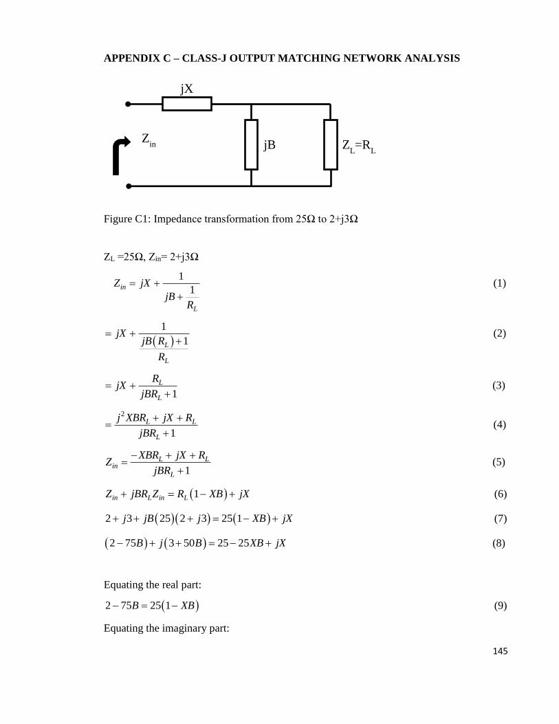
145
APPENDIX C – CLASS-J OUTPUT MATCHING NETWORK ANALYSIS
Figure C1: Impedance transformation from 25Ω to 2+j3Ω
ZL =25Ω, Zin= 2+j3Ω
1
1in
L
Z jX
jBR
(1)
1
1L
L
jXjB R
R
(2)
1
L
L
RjX
jBR
(3)
2
1
L L
L
j XBR jX R
jBR
(4)
1
L Lin
L
XBR jX RZ
jBR
(5)
1in L in LZ jBR Z R XB jX (6)
2 3 25 2 3 25 1j jB j XB jX (7)
2 75 3 50 25 25B j B XB jX (8)
Equating the real part:
2 75 25 1B XB (9)
Equating the imaginary part:
jX
jB ZL=R
L
Zin

146
3 50B X (10)
Insert (9) into (10):
2 75 25 1 3 50B B B (11)
46
50B (12)
Insert (12) into (10):
3 46X (13)
Therefore the respective components value is calculated as:
0
3 46L
(14)
and
0
46
50C
(15)