midterm exam statistics - university of california, berkeleyee247/fa07/files07/lectures/l18_f... ·...
TRANSCRIPT

EECS 247- Lecture 18 Nyquist Rate ADCs-Sampling © 2007 H.K. Page 1
Midterm Exam Statistics
0
1
2
3
4
5
6
10 15 16 17 17.5 18GradeMax.=20
Number of Occurrence
Mean=16Standard Deviation: 2
EECS 247- Lecture 18 Nyquist Rate ADCs-Sampling © 2007 H.K. Page 2
EE247Lecture 18
• ADC Converters– Sampling (continued)
• Sampling switch considerations– Switch induced distortion
• Sampling switch conductance dependence on input voltage
• Clock voltage boosters– Sampling switch charge injection & clock feedthrough
• Complementary switch• Use of dummy device• Bottom-plate switching
– Track & hold circuits– T/H circuit incorporating gain & offset cancellation

EECS 247- Lecture 18 Nyquist Rate ADCs-Sampling © 2007 H.K. Page 3
Summary of Last Lecture
• DAC Converters (continued)• Dynamic element matching
– DAC reconstruction filter• ADC Converters
– Sampling (continued)• Sampling switch considerations
– Thermal noise due to switch resistance– Sampling switch bandwidth limitations– Switch induced distortion
• Sampling switch conductance dependence on input voltage
EECS 247- Lecture 18 Nyquist Rate ADCs-Sampling © 2007 H.K. Page 4
Practical SamplingSummary So Far!
2
2212
B
BFS
C k TV
≥
( )1 for inON o o ox DD th
DD th
WVg g g C V VV V Lμ⎛ ⎞= − = −⎜ ⎟−⎝ ⎠
0.72
sR
B f C<<
• kT/C noise
• Finite Rsw limited bandwidth
• gsw = f (Vin) distortion
vINvOUT
CM1
φ1
EECS 247- Lecture 18 Nyquist Rate ADCs-Sampling © 2007 H.K. Page 5
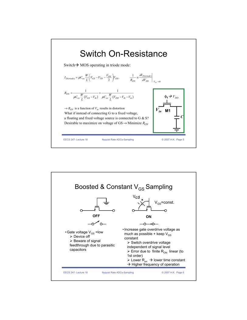
Switch On-ResistanceSwitch MOS operating in triode mode:
Vin
CM1
φ1 VDD( ) ( )
( )( )
0
1,2
1 1
is a function of results in distortionWhat if instead of connecting G to a fixed voltage,
DS
D triodeDSD triode ox GS TH DS
ON DS V
ON
ox GS th ox DD th in
ON in
dIW VI C V V VL R dV
R W WC V V C V V VL L
R V
μ
μ μ
→
⎛ ⎞= − − ≅⎜ ⎟⎝ ⎠
= =− − −
→
a floating and fixed voltage source is connected to G & S?Desirable to maximize on voltage of GS Minimize ONR→
EECS 247- Lecture 18 Nyquist Rate ADCs-Sampling © 2007 H.K. Page 6
Boosted & Constant VGS Sampling
VGS=const.
OFF ON
• Increase gate overdrive voltage as much as possible + keep VGSconstant
Switch overdrive voltage independent of signal level
Error due to finite RON linear (to 1st order)
Lower Ron lower time constantHigher frequency of operation
• Gate voltage VGS =lowDevice offBeware of signal
feedthrough due to parasitic capacitors
EECS 247- Lecture 18 Nyquist Rate ADCs-Sampling © 2007 H.K. Page 7
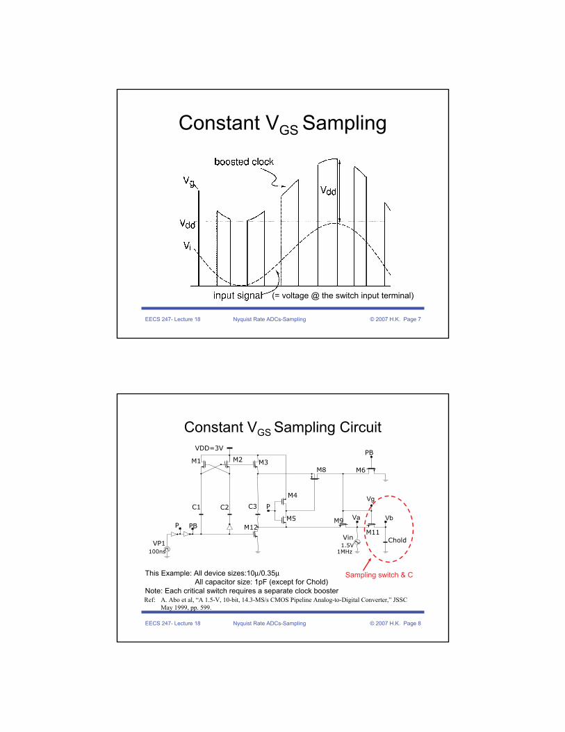
Constant VGS Sampling
(= voltage @ the switch input terminal)
EECS 247- Lecture 18 Nyquist Rate ADCs-Sampling © 2007 H.K. Page 8
Constant VGS Sampling Circuit
VP1100ns
M12
M8
M9
M6
M11Vin
1.5V1MHz
Chold
P
C1 C2
M1 M2
VDD=3V
M3
C3
M5
M4
P
This Example: All device sizes:10μ/0.35μAll capacitor size: 1pF (except for Chold)
Note: Each critical switch requires a separate clock booster
Vg
Va Vb
Sampling switch & C
PB
Ref: A. Abo et al, “A 1.5-V, 10-bit, 14.3-MS/s CMOS Pipeline Analog-to-Digital Converter,” JSSC May 1999, pp. 599.
PB
EECS 247- Lecture 18 Nyquist Rate ADCs-Sampling © 2007 H.K. Page 9
Clock Voltage Doubler Operation
C1 C2
M10ff
M2Saturation
mode
VP1=clock
PB
VDD=0 3V
P
a) Start–up
0 3V
0 3V 0 0
0 3V 0 (3V-VthM2)
Acquire charge C1 C2
M1Triode
M2off
VP1
PB
VDD=3V
P
3V 0
3V 0
3V 0 3V (3V-VthM2) (6V-Vth
M2)
b) Next clock transition
0 3V
VP1
EECS 247- Lecture 18 Nyquist Rate ADCs-Sampling © 2007 H.K. Page 10
Clock Voltage Doubler Operation
C1 C2
M10ff
M2
VP1
PB
VDD=3V
P
0 3V
0 3V
3V ~6V
3V 0
c) Next clock phase
(6V-VthM2) (3V-Vth
M2) ~ 3V
M2Triode
Acquires charge
• Both C1 & C2 charged to
VDD after one clock cycle
• Note that bottom plate of C1 & C2 is either 0 or VDD while top plates are at VDD or 2VDD
EECS 247- Lecture 18 Nyquist Rate ADCs-Sampling © 2007 H.K. Page 11
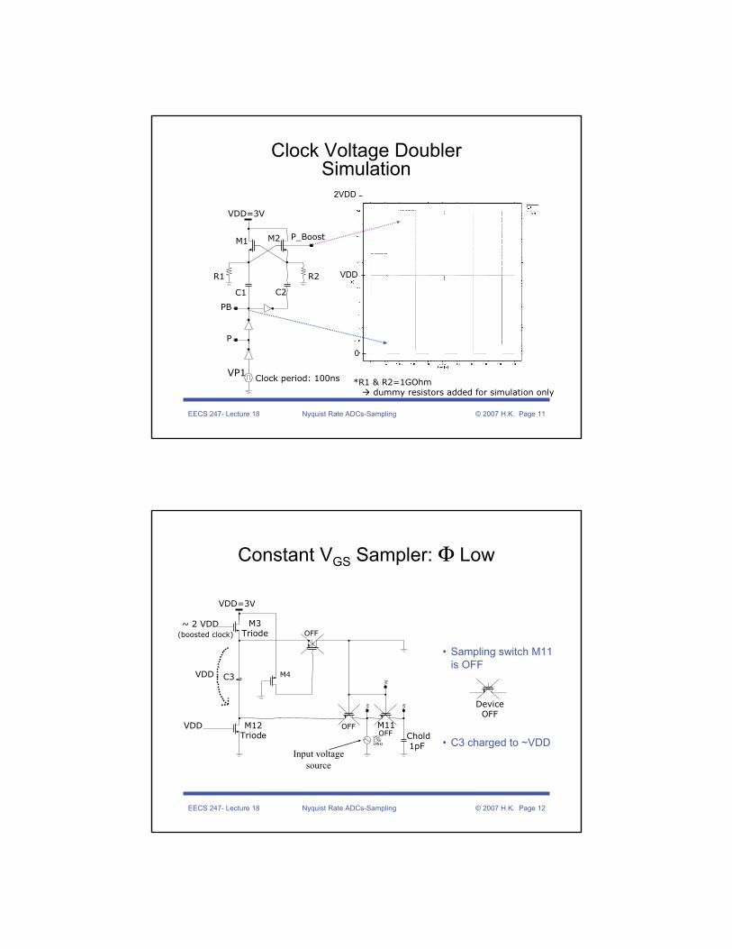
Clock Voltage DoublerSimulation
C1 C2
M1 M2
VP1Clock period: 100ns
PB
P_Boost
VDD
2VDD
0
VDD=3V
R1 R2
*R1 & R2=1GOhmdummy resistors added for simulation only
P
EECS 247- Lecture 18 Nyquist Rate ADCs-Sampling © 2007 H.K. Page 12
Constant VGS Sampler: Φ Low
• Sampling switch M11 is OFF
• C3 charged to ~VDDInput voltage
source
M3Triode
C3
M12Triode
M4
OFF
VS11.5V1MHz
Chold1pF
~ 2 VDD(boosted clock)
VDD
VDD
OFF M11OFF
DeviceOFF
VDD=3V
EECS 247- Lecture 18 Nyquist Rate ADCs-Sampling © 2007 H.K. Page 13
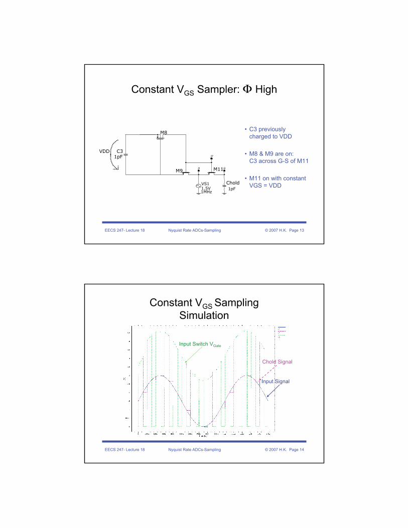
Constant VGS Sampler: Φ High
• C3 previously charged to VDD
• M8 & M9 are on:C3 across G-S of M11
• M11 on with constant VGS = VDD
C31pF
M8
M9 M11
VS11.5V1MHz
Chold1pF
VDD
EECS 247- Lecture 18 Nyquist Rate ADCs-Sampling © 2007 H.K. Page 14
Constant VGS SamplingSimulation
Input Switch VGate
Input Signal
Chold Signal
EECS 247- Lecture 18 Nyquist Rate ADCs-Sampling © 2007 H.K. Page 15
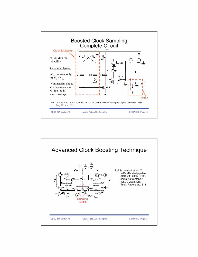
Boosted Clock Sampling Complete Circuit
Ref: A. Abo et al, “A 1.5-V, 10-bit, 14.3-MS/s CMOS Pipeline Analog-to-Digital Converter,” JSSC May 1999, pp. 599.
Clock Multiplier
Switch
M7 & M13 for reliability
Remaining issues:
-VGS constant only for Vin <Vout
-Nonlinearity due to Vth dependence of M11on body-source voltage
EECS 247- Lecture 18 Nyquist Rate ADCs-Sampling © 2007 H.K. Page 16
Advanced Clock Boosting Technique
Ref: M. Waltari et al., "A self-calibrated pipeline ADC with 200MHz IF-sampling frontend," ISSCC 2002, Dig. Tech. Papers, pp. 314
Sampling Switch
EECS 247- Lecture 18 Nyquist Rate ADCs-Sampling © 2007 H.K. Page 17
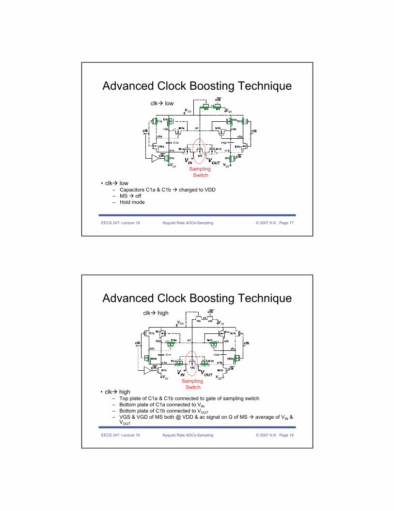
Advanced Clock Boosting Technique
• clk low– Capacitors C1a & C1b charged to VDD– MS off– Hold mode
Sampling Switch
clk low
EECS 247- Lecture 18 Nyquist Rate ADCs-Sampling © 2007 H.K. Page 18
Advanced Clock Boosting Technique
Sampling Switch
• clk high– Top plate of C1a & C1b connected to gate of sampling switch– Bottom plate of C1a connected to VIN– Bottom plate of C1b connected to VOUT– VGS & VGD of MS both @ VDD & ac signal on G of MS average of VIN &
VOUT
clk high
EECS 247- Lecture 18 Nyquist Rate ADCs-Sampling © 2007 H.K. Page 19
Advanced Clock Boosting Technique
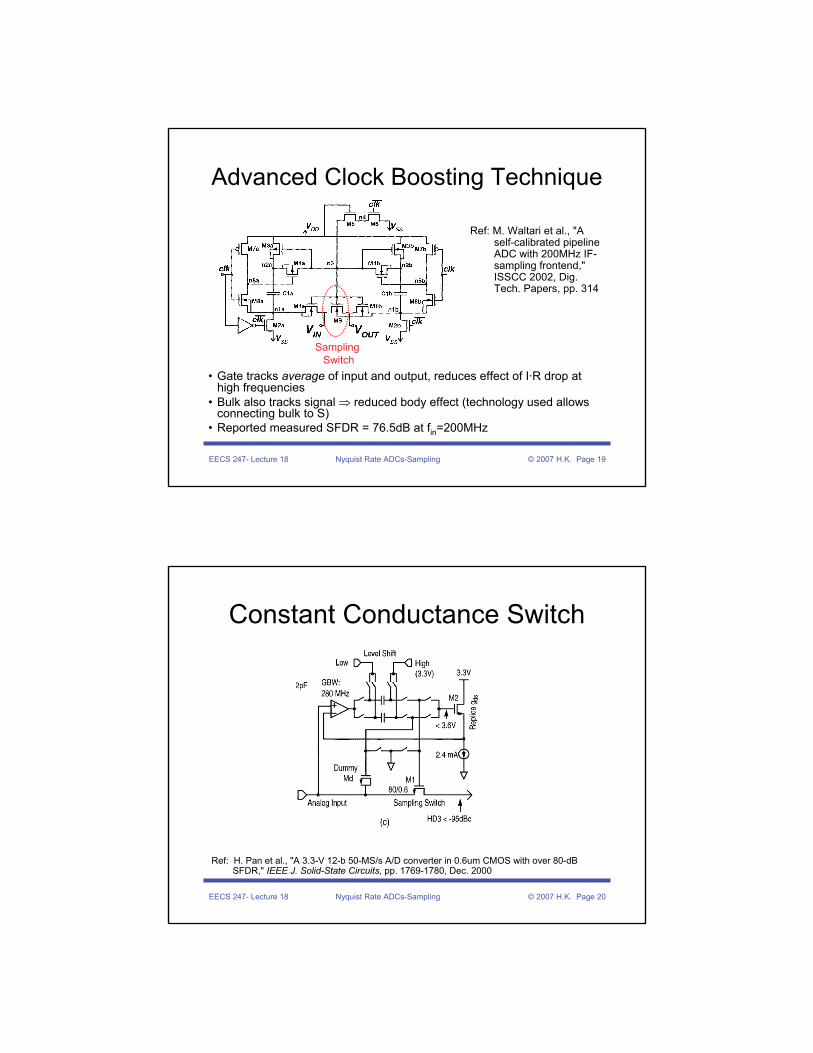
• Gate tracks average of input and output, reduces effect of I·R drop at high frequencies
• Bulk also tracks signal ⇒ reduced body effect (technology used allows connecting bulk to S)
• Reported measured SFDR = 76.5dB at fin=200MHz
Ref: M. Waltari et al., "A self-calibrated pipeline ADC with 200MHz IF-sampling frontend," ISSCC 2002, Dig. Tech. Papers, pp. 314
Sampling Switch
EECS 247- Lecture 18 Nyquist Rate ADCs-Sampling © 2007 H.K. Page 20
Constant Conductance Switch
Ref: H. Pan et al., "A 3.3-V 12-b 50-MS/s A/D converter in 0.6um CMOS with over 80-dB SFDR," IEEE J. Solid-State Circuits, pp. 1769-1780, Dec. 2000

EECS 247- Lecture 18 Nyquist Rate ADCs-Sampling © 2007 H.K. Page 21
Constant Conductance Switch
Ref: H. Pan et al., "A 3.3-V 12-b 50-MS/s A/D converter in 0.6um CMOS with over 80-dB SFDR," IEEE J. Solid-State Circuits, pp. 1769-1780, Dec. 2000
OFF
EECS 247- Lecture 18 Nyquist Rate ADCs-Sampling © 2007 H.K. Page 22
Constant Conductance Switch
Ref: H. Pan et al., "A 3.3-V 12-b 50-MS/s A/D converter in 0.6um CMOS with over 80-dB SFDR," IEEE J. Solid-State Circuits, pp. 1769-1780, Dec. 2000
ON
M2 Constant currentconstant gds
M1 replica of M2 & same VGSas M2M1 alsoconstant gds
• Note: Authors report requirement of 280MHz GBW for the opamp for 12bit 50Ms/s ADC
• Also, opamp common-mode compliance for full input range required
EECS 247- Lecture 18 Nyquist Rate ADCs-Sampling © 2007 H.K. Page 23
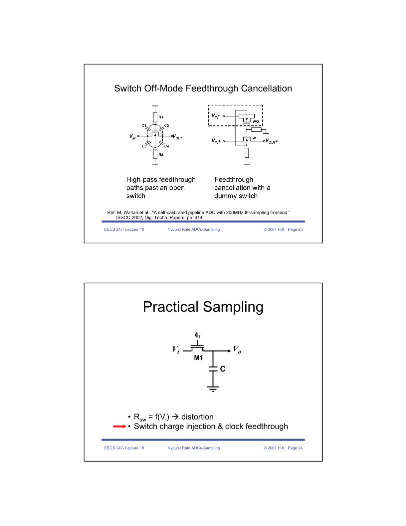
Switch Off-Mode Feedthrough Cancellation
Ref: M. Waltari et al., "A self-calibrated pipeline ADC with 200MHz IF-sampling frontend," ISSCC 2002, Dig. Techn. Papers, pp. 314
EECS 247- Lecture 18 Nyquist Rate ADCs-Sampling © 2007 H.K. Page 24
Practical Sampling
Vo
CM1
φ1
• Rsw = f(Vi) distortion• Switch charge injection & clock feedthrough
Vi
EECS 247- Lecture 18 Nyquist Rate ADCs-Sampling © 2007 H.K. Page 25
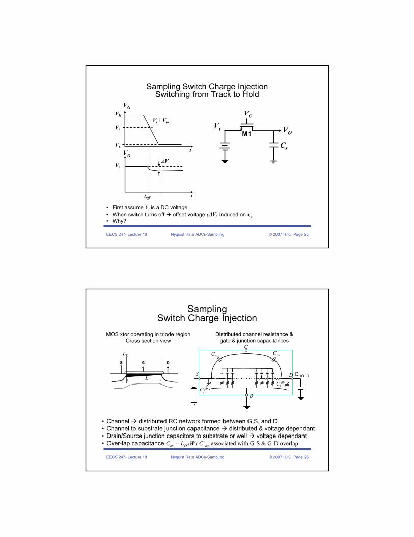
Sampling Switch Charge Injection Switching from Track to Hold
Vi VO
Cs
M1
VG
• First assume Vi is a DC voltage• When switch turns off offset voltage (ΔV) induced on Cs• Why?
VG
t
VH
Vi
VL
Vi +Vth
VO
Vi
toff
ΔV
t
EECS 247- Lecture 18 Nyquist Rate ADCs-Sampling © 2007 H.K. Page 26
SamplingSwitch Charge Injection
• Channel distributed RC network formed between G,S, and D• Channel to substrate junction capacitance distributed & voltage dependant• Drain/Source junction capacitors to substrate or well voltage dependant• Over-lap capacitance Cov = LDxWx C’ox associated with G-S & G-D overlap
MOS xtor operating in triode regionCross section view
Distributed channel resistance & gate & junction capacitances
S
G
D
B
LD
L
Cov Cov
Cjdb
Cjsb
CHOLD
EECS 247- Lecture 18 Nyquist Rate ADCs-Sampling © 2007 H.K. Page 27
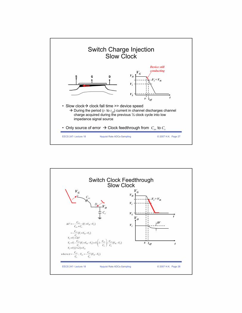
Switch Charge Injection Slow Clock
• Slow clock clock fall time >> device speed During the period (t- to toff) current in channel discharges channel charge acquired during the previous ½ clock cycle into low impedance signal source
• Only source of error Clock feedthrough from Cov to Cs
VG
t
VH
Vi
VL
Vi +Vth
tofft-
Device still conducting
EECS 247- Lecture 18 Nyquist Rate ADCs-Sampling © 2007 H.K. Page 28
Switch Clock Feedthrough Slow Clock
VG
t
VH
Vi
VL
Vi +Vth
VO
Vi
toff
ΔV
t
D
Cov
VG
( )
( )
( ) ( )
( )
( )
ovi th L
ov s
ovi th L
so i
ov ov ovo i i th L i th L
s s so i os
ov ovos th L
s s
CV V V V
C C
CV V V
CV V V
C C CV V V V V V 1 V V
C C CV V 1 V
C Cwhere ; V V V
C C
ε
ε
Δ = − + −+
≈ − + −
= + Δ⎛ ⎞
= − + − = − − −⎜ ⎟⎜ ⎟⎝ ⎠
= + +
= − = − −
t-
Cs
VO
EECS 247- Lecture 18 Nyquist Rate ADCs-Sampling © 2007 H.K. Page 29
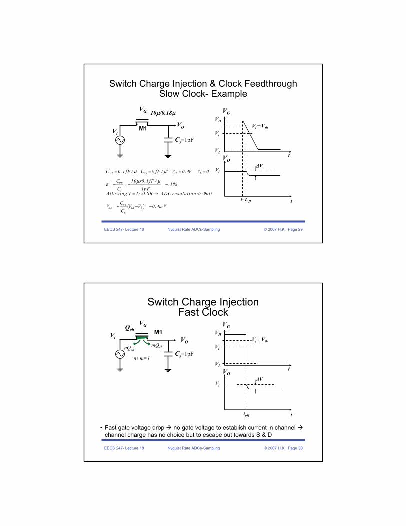
Switch Charge Injection & Clock Feedthrough Slow Clock- Example
( )
' 2ov ox th L
ov
s
ovos th L
s
C 0.1 fF / C 9 fF / V 0.4V V 0
C 10 x0.1 fF /.1%
C 1pFAllowing 1/ 2LSB ADC resolut ion ~ 9bit
CV V V 0.4mV
C
μ μ
μ με
ε
= = = =
= − = − = −
= → <
= − − = −
VG
t
VH
Vi
VL
Vi +Vth
VO
Vi
toff
ΔV
t
Vi
VO
Cs=1pF
M1
VG 10μ/0.18μ
t-
EECS 247- Lecture 18 Nyquist Rate ADCs-Sampling © 2007 H.K. Page 30
Switch Charge Injection Fast Clock
VG
t
VH
Vi
VL
Vi +Vth
VO
Vi
toff
ΔV
t
Vi VO
Cs=1pF
M1VG
• Fast gate voltage drop no gate voltage to establish current in channel channel charge has no choice but to escape out towards S & D
Qch
mQchnQch
n+m=1
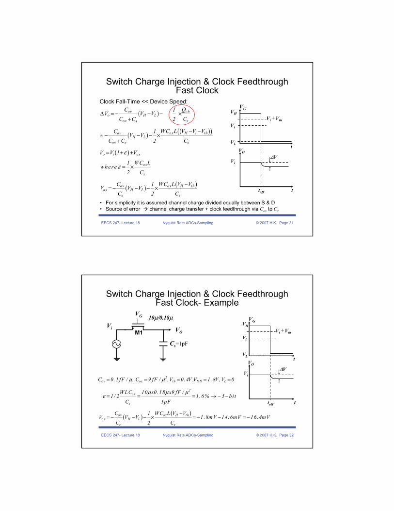
EECS 247- Lecture 18 Nyquist Rate ADCs-Sampling © 2007 H.K. Page 31
• For simplicity it is assumed channel charge divided equally between S & D • Source of error channel charge transfer + clock feedthrough via Cov to Cs
VG
t
VH
Vi
VL
Vi +Vth
VO
Vi
toff
ΔV
t
Switch Charge Injection & Clock FeedthroughFast Clock
Clock Fall-Time << Device Speed:
( )
( ) ( )( )
( )
( ) ( )
ov cho H L
ov s s
ox H i thovH L
ov s s
o i os
ox
s
ov ox H thos H L
s s
C 1 QV V V
C C 2 C
WC L V V VC 1V V
C C 2 C
V V 1 V
1 WC Lwhere
2 C
C 1 WC L V VV V V
C 2 C
ε
ε
Δ = − − − ×+
− −≈ − − − ×
+
= + +
= ×
−= − − − ×
EECS 247- Lecture 18 Nyquist Rate ADCs-Sampling © 2007 H.K. Page 32
Switch Charge Injection & Clock FeedthroughFast Clock- Example
Vi VO
Cs=1pF
M1
VG 10μ/0.18μ VG
t
VH
Vi
VL
Vi +Vth
VO
Vi
toff
ΔV
t
( ) ( )
2ov ox th DD L
2ox
s
ov ox H thos H L
s s
C 0.1 fF / , C 9 fF / V 0.4V ,V 1.8V ,V 0
WLC 10 x0.18 x9 fF /1/ 2 1.6% ~ 5 bi t
C 1pF
C 1 WC L V VV V V 1.8mV 14.6mV 16.4mV
C 2 C
,μ μ
μ μ με
= = = = =
= = = → −
−= − − − × = − − = −

EECS 247- Lecture 18 Nyquist Rate ADCs-Sampling © 2007 H.K. Page 33
Vo
ΔV
Vi
Switch Charge Injection & Clock FeedthroughSlow Clock versus Fast Clock
Slow Clock
Vo
ΔV
Vi
Fast Clock
EECS 247- Lecture 18 Nyquist Rate ADCs-Sampling © 2007 H.K. Page 34
Switch Charge Injection & Clock FeedthroughExample-Summary
Error function of:Clock fall time Input voltage level Source impedance Sampling capacitanceSwitch size
Clock fall/rise should be well-controlled & not to be faster (sharper) than necessary
Clock fall time
ε VOS
Clock fall time
1.6%
-.1%
16mV
0.4mV
EECS 247- Lecture 18 Nyquist Rate ADCs-Sampling © 2007 H.K. Page 35
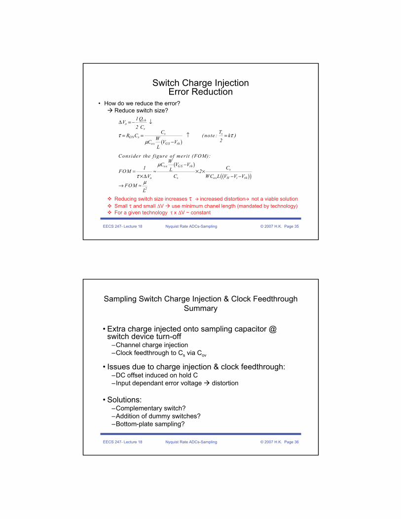
Switch Charge InjectionError Reduction
( )
( )
( )( )
cho
ss s
ON s
ox GS th
ox GS ths
o s ox H i th
2
1 QV
2 CC T
R C ( note : kW 2C V VL
Consider the f igure of meri t (FOM):W
C V V1 CLFOM 2V C WC L V V V
FOML
)μ
μ
μ
τ τ
τ
Δ = − ↓
= = ↑ =−
−= ≈ ×
Δ − −
→ ≈
××
• How do we reduce the error? Reduce switch size?
Reducing switch size increases τ increased distortion not a viable solutionSmall τ and small ΔV use minimum chanel length (mandated by technology)For a given technology τ x ΔV ~ constant
EECS 247- Lecture 18 Nyquist Rate ADCs-Sampling © 2007 H.K. Page 36
Sampling Switch Charge Injection & Clock FeedthroughSummary
• Extra charge injected onto sampling capacitor @ switch device turn-off
–Channel charge injection–Clock feedthrough to Cs via Cov
• Issues due to charge injection & clock feedthrough:–DC offset induced on hold C–Input dependant error voltage distortion
• Solutions:–Complementary switch?–Addition of dummy switches?–Bottom-plate sampling?
EECS 247- Lecture 18 Nyquist Rate ADCs-Sampling © 2007 H.K. Page 37
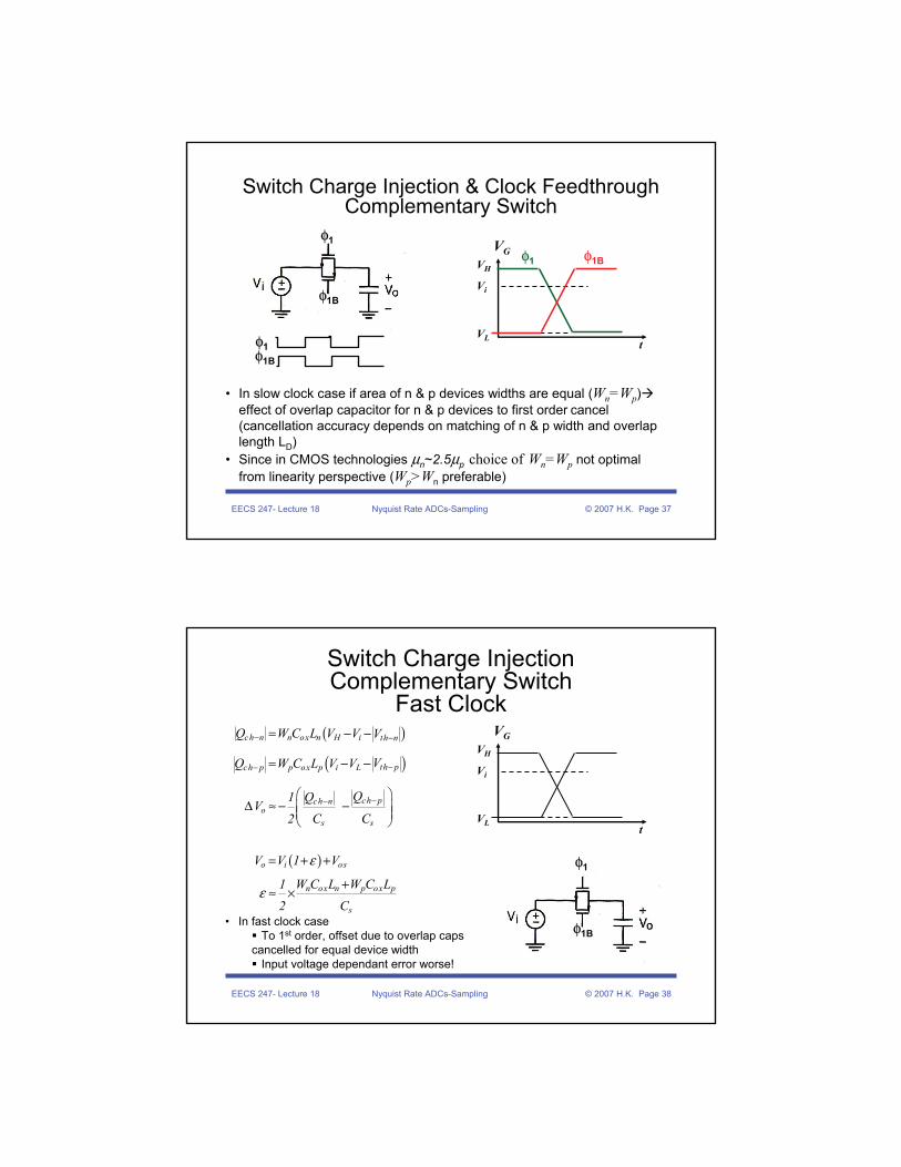
Switch Charge Injection & Clock FeedthroughComplementary Switch
• In slow clock case if area of n & p devices widths are equal (Wn=Wp)effect of overlap capacitor for n & p devices to first order cancel (cancellation accuracy depends on matching of n & p width and overlap length LD)
• Since in CMOS technologies μn~2.5μp choice of Wn=Wp not optimal from linearity perspective (Wp>Wn preferable)
φ1φ1B
φ1
φ1B
VG
t
VH
Vi
VL
φ1 φ1B
EECS 247- Lecture 18 Nyquist Rate ADCs-Sampling © 2007 H.K. Page 38
Switch Charge Injection Complementary Switch
Fast Clock
• In fast clock case To 1st order, offset due to overlap caps
cancelled for equal device widthInput voltage dependant error worse!
φ1
φ1B
VG
t
VH
Vi
VL
( )
( )
( )
ch n n ox n H i th n
th pch p p ox p i L
ch pch no
s s
o i os
n ox n p ox p
s
Q W C L V V V
VQ W C L V V
Q1 QV
2 C C
V V 1 V
1 W C L W C L2 C
ε
ε
− −
−−
−−
= − −
= − −
⎛ ⎞Δ ≈ − −⎜ ⎟⎜ ⎟
⎝ ⎠
= + +
+≈ ×
EECS 247- Lecture 18 Nyquist Rate ADCs-Sampling © 2007 H.K. Page 39
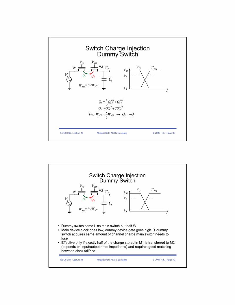
Switch Charge InjectionDummy Switch
Vi
VO
Cs
t
VH
Vi
VL
VG VGB
WM2=1/2WM1
VG VGB
M1 M2
M 1 M 11 ch ov
M 2 M 22 ch ov
M 2 M 1 2 1
1Q Q Q
2Q Q 2Q
1For W W Q Q
2
≈ +
≈ +
= → = −
Q1 Q2
EECS 247- Lecture 18 Nyquist Rate ADCs-Sampling © 2007 H.K. Page 40
Switch Charge InjectionDummy Switch
Vi
VO
Cs
t
VH
Vi
VL
VG VGB
• Dummy switch same L as main switch but half W • Main device clock goes low, dummy device gate goes high dummy
switch acquires same amount of channel charge main switch needs to lose
• Effective only if exactly half of the charge stored in M1 is transferred to M2 (depends on input/output node impedance) and requires good matching between clock fall/rise
WM2=1/2WM1
VG VGB
M1 M2
Q1 Q2
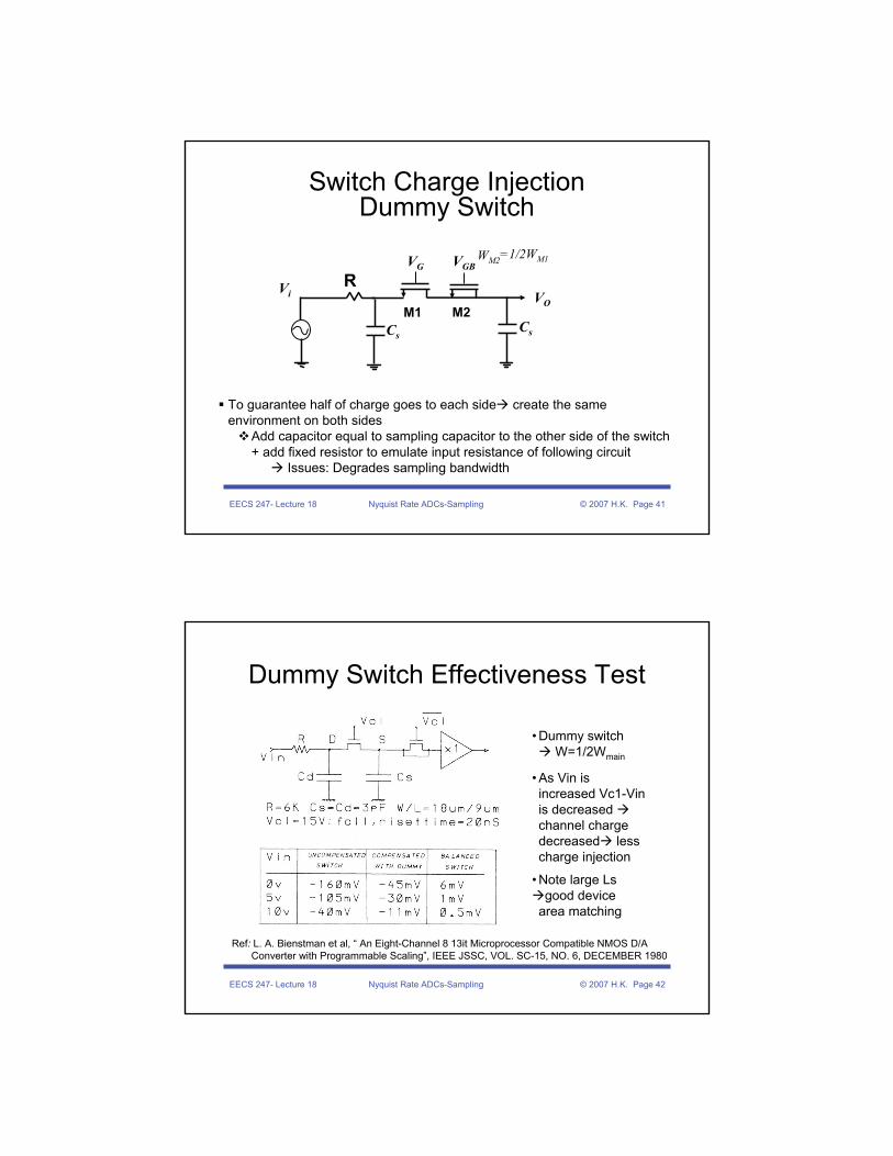
EECS 247- Lecture 18 Nyquist Rate ADCs-Sampling © 2007 H.K. Page 41
Switch Charge InjectionDummy Switch
Vi VOM1
VG
M2
VGB
To guarantee half of charge goes to each side create the same environment on both sides
Add capacitor equal to sampling capacitor to the other side of the switch + add fixed resistor to emulate input resistance of following circuit
Issues: Degrades sampling bandwidth
CsCs
RWM2=1/2WM1
EECS 247- Lecture 18 Nyquist Rate ADCs-Sampling © 2007 H.K. Page 42
Dummy Switch Effectiveness Test
Ref: L. A. Bienstman et al, “ An Eight-Channel 8 13it Microprocessor Compatible NMOS D/A Converter with Programmable Scaling”, IEEE JSSC, VOL. SC-15, NO. 6, DECEMBER 1980
• Dummy switch W=1/2Wmain
• As Vin is increased Vc1-Vin is decreased channel charge decreased less charge injection
• Note large Lsgood device
area matching
EECS 247- Lecture 18 Nyquist Rate ADCs-Sampling © 2007 H.K. Page 43
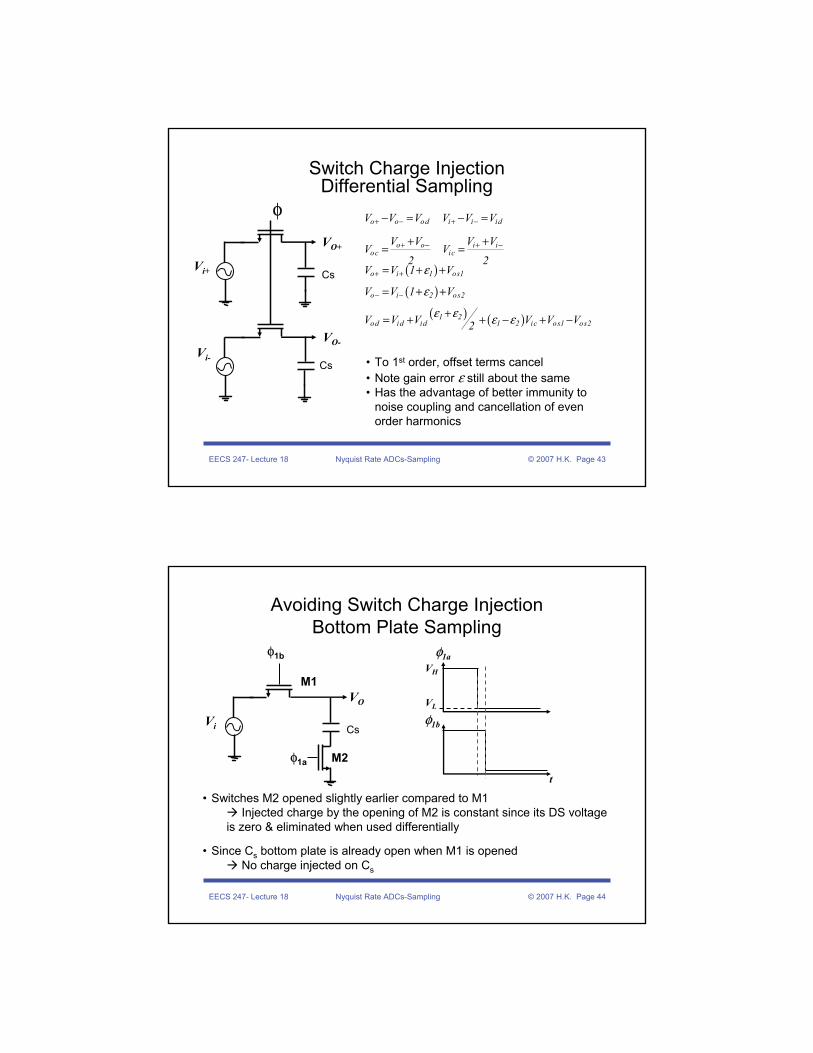
Switch Charge InjectionDifferential Sampling
Vi+
VO+
Vi-
VO-
• To 1st order, offset terms cancel• Note gain error ε still about the same• Has the advantage of better immunity to
noise coupling and cancellation of even order harmonics
φ
Cs
Cs
( )( )
( ) ( )
o o od i i id
o o i ioc ic
o i 1 os1
o i 2 os2
1 2od id id 1 2 ic os1 os2
V V V V V V
V V V VV V
2 2V V 1 V
V V 1 V
V V V V V V2
ε
ε
ε ε ε ε
+ − + −
+ − + −
+ +
− −
− = − =
+ += =
= + +
= + +
+= + + − + −
EECS 247- Lecture 18 Nyquist Rate ADCs-Sampling © 2007 H.K. Page 44
Avoiding Switch Charge InjectionBottom Plate Sampling
• Switches M2 opened slightly earlier compared to M1Injected charge by the opening of M2 is constant since its DS voltage
is zero & eliminated when used differentially
• Since Cs bottom plate is already open when M1 is openedNo charge injected on Cs
φ1aVH
VL
t
φ1bVi
VO
M1
φ1b
φ1a M2
Cs
EECS 247- Lecture 18 Nyquist Rate ADCs-Sampling © 2007 H.K. Page 45
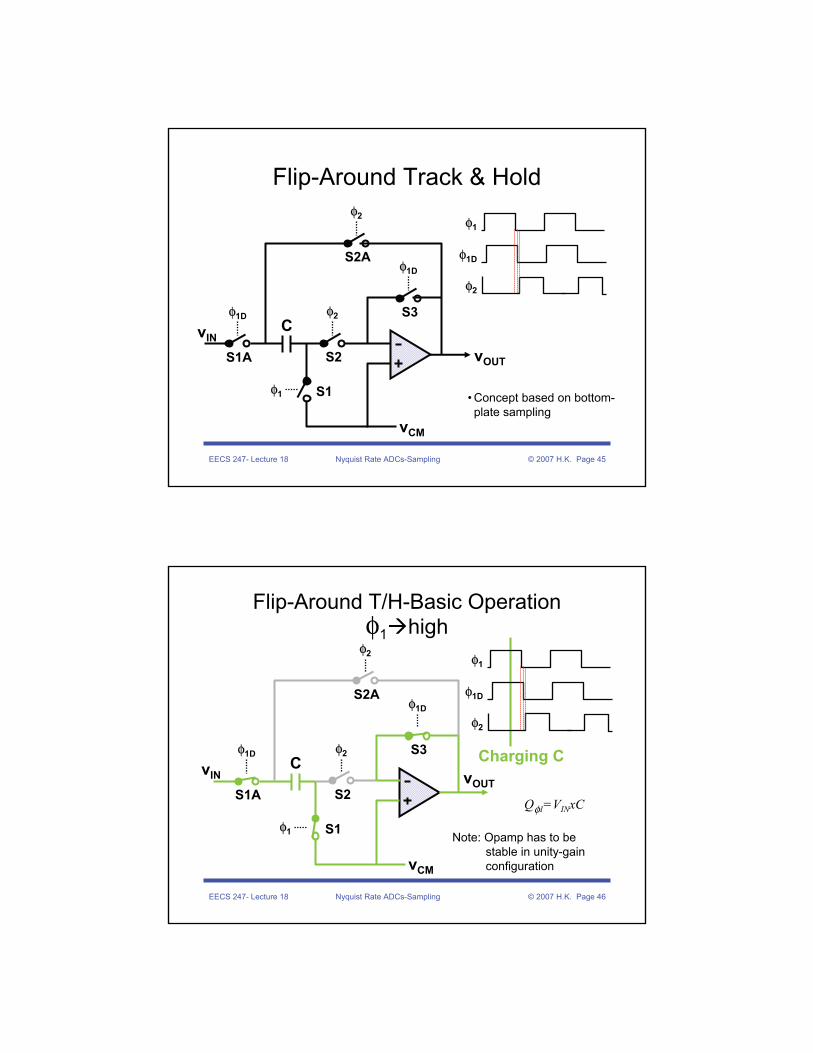
Flip-Around Track & Hold
vIN
vOUT
C
S1A
φ1D
S2
φ2
S2A
φ2
S3
φ1D
φ1 S1
vCM
• Concept based on bottom-plate sampling
φ1
φ2
φ1D
EECS 247- Lecture 18 Nyquist Rate ADCs-Sampling © 2007 H.K. Page 46
Flip-Around T/H-Basic Operationφ1 high
vIN vOUT
C
S1A
φ1D
S2
φ2
S2A
φ2
S3
φ1D
φ1 S1
vCM
Charging C
φ1
φ1D
φ2
Note: Opamp has to be stable in unity-gain configuration
Qφ1=VINxC
EECS 247- Lecture 18 Nyquist Rate ADCs-Sampling © 2007 H.K. Page 47
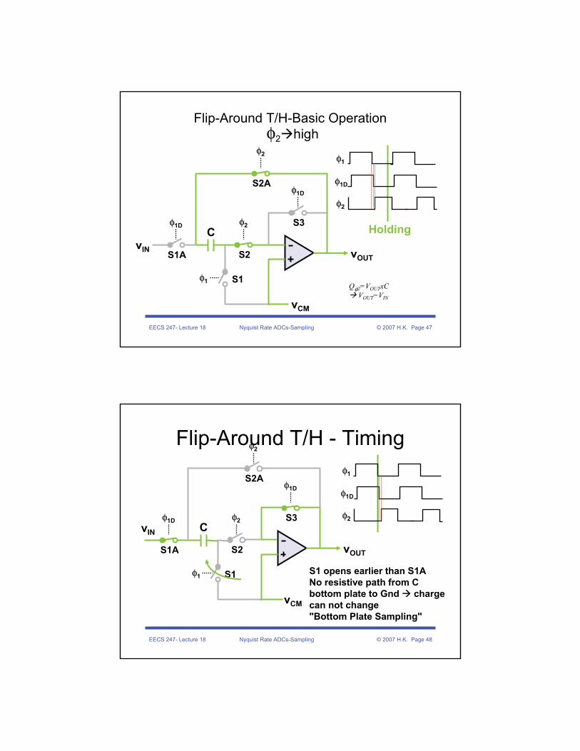
Flip-Around T/H-Basic Operationφ2 high
vIN vOUT
C
S1A
φ1D
S2
φ2
S2A
φ2
S3
φ1D
φ1 S1
vCM
Holding
φ1
φ2
φ1D
Qφ2=VOUTxCVOUT=VIN
EECS 247- Lecture 18 Nyquist Rate ADCs-Sampling © 2007 H.K. Page 48
Flip-Around T/H - Timing
S1 opens earlier than S1ANo resistive path from C bottom plate to Gnd charge can not change"Bottom Plate Sampling"
vIN
vOUT
C
S1A
φ1D
S2
φ2
S2A
φ2
S3
φ1D
φ1 S1
vCM
φ1
φ2
φ1D
EECS 247- Lecture 18 Nyquist Rate ADCs-Sampling © 2007 H.K. Page 49
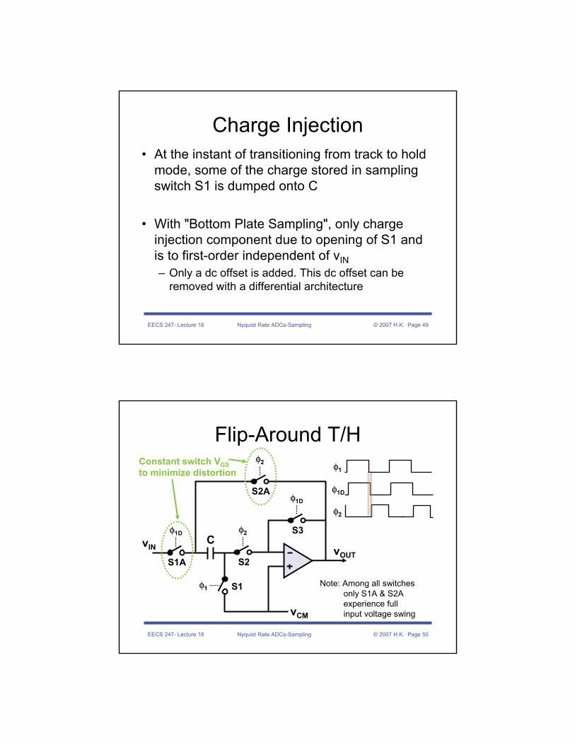
Charge Injection• At the instant of transitioning from track to hold
mode, some of the charge stored in sampling switch S1 is dumped onto C
• With "Bottom Plate Sampling", only charge injection component due to opening of S1 and is to first-order independent of vIN– Only a dc offset is added. This dc offset can be
removed with a differential architecture
EECS 247- Lecture 18 Nyquist Rate ADCs-Sampling © 2007 H.K. Page 50
Flip-Around T/H
vIN vOUT
C
S1A
φ1D
S2
φ2
S2A
φ2
S3
φ1D
φ1 S1
vCM
Constant switch VGSto minimize distortion
Note: Among all switches only S1A & S2A experience full input voltage swing
φ1
φ2
φ1D

EECS 247- Lecture 18 Nyquist Rate ADCs-Sampling © 2007 H.K. Page 51
Flip-Around T/H• S1 is chosen to be an n-channel MOSFET• Since it always switches the same voltage, it’s on-
resistance, RS1, is signal-independent (to first order) • Choosing RS1 >> RS1A minimizes the non-linear
component of R = RS1A+ RS1– Typically, S1A is a wide (much lower resistance than S1) &
constant VGS switch– In practice size of S1A is limited by the (nonlinear) S/D
capacitance that also adds distortion– If S1A’s resistance is negligible delay depends only on S1
resistance– S1 resistance is independent of VIN error due to finite
time-constant independent of VIN
EECS 247- Lecture 18 Nyquist Rate ADCs-Sampling © 2007 H.K. Page 52
Differential Flip-Around T/H
Ref: W. Yang, et al. “A 3-V 340-mW 14-b 75-Msample/s CMOS ADC With 85-dB SFDR at Nyquist Input,” IEEE JOURNAL OF SOLID-STATE CIRCUITS, VOL. 36, NO. 12, DECEMBER 2001 1931
Offset voltage associated with charge injection of S11 & S12 cancelled by differential nature of the circuitDuring input sampling phase amp outputs shorted together
S11
S12
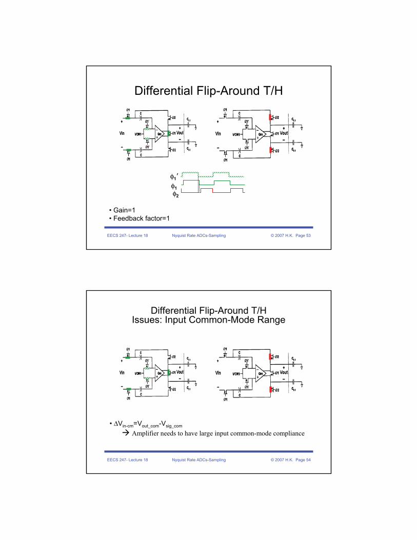
EECS 247- Lecture 18 Nyquist Rate ADCs-Sampling © 2007 H.K. Page 53
Differential Flip-Around T/H
• Gain=1• Feedback factor=1
φ1’φ1φ2
EECS 247- Lecture 18 Nyquist Rate ADCs-Sampling © 2007 H.K. Page 54
Differential Flip-Around T/HIssues: Input Common-Mode Range
• ΔVin-cm=Vout_com-Vsig_com
Amplifier needs to have large input common-mode compliance
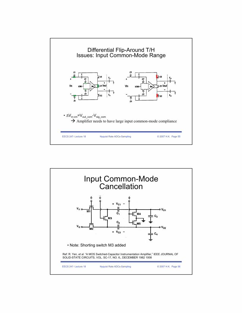
EECS 247- Lecture 18 Nyquist Rate ADCs-Sampling © 2007 H.K. Page 55
Differential Flip-Around T/HIssues: Input Common-Mode Range
• ΔVin-cm=Vout_com-Vsig_com
Amplifier needs to have large input common-mode compliance
EECS 247- Lecture 18 Nyquist Rate ADCs-Sampling © 2007 H.K. Page 56
Input Common-Mode Cancellation
Ref: R. Yen, et al. “A MOS Switched-Capacitor Instrumentation Amplifier,” IEEE JOURNAL OF SOLID-STATE CIRCUITS, VOL. SC-17, NO. 6,, DECEMBER 1982 1008
• Note: Shorting switch M3 added
EECS 247- Lecture 18 Nyquist Rate ADCs-Sampling © 2007 H.K. Page 57
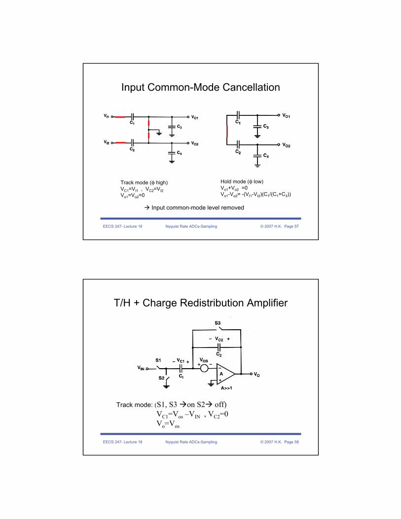
Input Common-Mode Cancellation
Track mode (φ high)VC1=VI1 , VC2=VI2Vo1=Vo2=0
Hold mode (φ low)Vo1+Vo2 =0Vo1-Vo2= -(VI1-VI2)(C1/(C1+C3))
Input common-mode level removed
EECS 247- Lecture 18 Nyquist Rate ADCs-Sampling © 2007 H.K. Page 58
T/H + Charge Redistribution Amplifier
Track mode: (S1, S3 on S2 off)VC1=Vos –VIN , VC2=0Vo=Vos
EECS 247- Lecture 18 Nyquist Rate ADCs-Sampling © 2007 H.K. Page 59
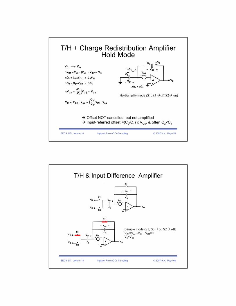
T/H + Charge Redistribution AmplifierHold Mode
Hold/amplify mode (S1, S3 off S2 on)
Offset NOT cancelled, but not amplifiedInput-referred offset =(C2/C1) x VOS, & often C2<C1
2
1
2
EECS 247- Lecture 18 Nyquist Rate ADCs-Sampling © 2007 H.K. Page 60
T/H & Input Difference Amplifier
Sample mode (S1, S3 on S2 off)VC1=Vos –VI1 , VC2=0Vo=Vos