marvell (88ap3xx) processor - toradex · marvell may make changes to these specifications at any...
TRANSCRIPT
Marvell. Moving Forward Faster
Doc. No. MV-S301374-02, Revision 2.0 Version -
April 6, 2009 Released
Cover
Marvell® PXA3xx (88AP3xx) Processor FamilyVol. II: Memory Controller Configuration Developers ManualPXA30x Processor (88AP300, 88AP301, 88AP302, 88AP303)
PXA31x Processor (88AP310, 88AP311, 88AP312)
PXA320 Processor (88AP320, 88AP322)
Document Conventions
Note: Provides related information or information of special importance.
Caution: Indicates potential damage to hardware or software, or loss of data.
Warning: Indicates a risk of personal injury.
Document Status Draft For internal use. This document has not passed a complete technical review cycle and ECN signoff
process.
Preliminary Tapeout (Advance)
This document contains design specifications for a product in its initial stage of design and development. A revision of this document or supplementary information may be published at a later date. Marvell may make changes to these specifications at any time without notice.Contact Marvell Field Application Engineers for more information.
Preliminary Information
This document contains preliminary specifications. A revision of this document or supplementary information may be published at a later date. Marvell may make changes to these specifications at any time without notice. . Contact Marvell Field Application Engineers for more information.
Complete Information
This document contains specifications for a product in its final qualification stages. Marvell may make changes to these specifications at any time without notice. Contact Marvell Field Application Engineers for more information.
Doc Status: Preliminary Technical Publication: 2.00
X . Y ZMilestone Indicator:Draft = 0.xxAdvance = 1.xxPreliminary = 2.xx Various Revisions Indicator
Work in Progress IndicatorZero means document is released.
For more information, visit our website at: www.marvell.comDisclaimerNo part of this document may be reproduced or transmitted in any form or by any means, electronic or mechanical, including photocopying and recording, for any purpose, without the express written permission of Marvell. Marvell retains the right to make changes to this document at any time, without notice. Marvell makes no warranty of any kind, expressed or implied, with regard to any information contained in this document, including, but not limited to, the implied warranties of merchantability or fitness for any particular purpose. Further, Marvell does not warrant the accuracy or completeness of the information, text, graphics, or other items contained within this document. Marvell products are not designed for use in life-support equipment or applications that would cause a life-threatening situation if any such products failed. Do not use Marvell products in these types of equipment or applications. With respect to the products described herein, the user or recipient, in the absence of appropriate U.S. government authorization, agrees: 1) Not to re-export or release any such information consisting of technology, software or source code controlled for national security reasons by the U.S. Export Control Regulations ("EAR"), to a national of EAR Country Groups D:1 or E:2; 2) Not to export the direct product of such technology or such software, to EAR Country Groups D:1 or E:2, if such technology or software and direct products thereof are controlled for national security reasons by the EAR; and, 3) In the case of technology controlled for national security reasons under the EAR where the direct product of the technology is a complete plant or component of a plant, not to export to EAR Country Groups D:1 or E:2 the direct product of the plant or major component thereof, if such direct product is controlled for national security reasons by the EAR, or is subject to controls under the U.S. Munitions List ("USML"). At all times hereunder, the recipient of any such information agrees that they shall be deemed to have manually signed this document in connection with their receipt of any such information. Copyright © 2009. Marvell International Ltd. All rights reserved. Marvell, the Marvell logo, Moving Forward Faster, Alaska, Fastwriter, Datacom Systems on Silicon, Libertas, Link Street, NetGX, PHYAdvantage, Prestera, Raising The Technology Bar, The Technology Within, Virtual Cable Tester, and Yukon are registered trademarks of Marvell. Ants, AnyVoltage, Discovery, DSP Switcher, Feroceon, GalNet, GalTis, Horizon, Marvell Makes It All Possible, RADLAN, UniMAC, and VCT are trademarks of Marvell. Intel XScale® is a trademark or registered trademark of Intel Corporation or its subsidiaries in the United States and other countries. All other trademarks are the property of their respective owners.
PXA3xx (88AP3xx) Processor Family Vol. II: Memory Controller Configuration Developers Manual
Doc. No. MV-S301374-02 Revision 2.0 Version -
Copyright © 2009 Marvell
Page 2 April 6, 2009 Released
1234567891011121314151617181920212223242526272829303132333435363738394041424344454647484950515253545556575859
Contents
Copyright © 2009 Marvell Doc. No. MV-S301374-02 Rev. 2.0Version -
April 6, 2009 Released Page 3
Contents
1 Dynamic Memory Controller.......................................................................................................13
1.1 External Memory Pin Interface (EMPI)............................................................................................................131.1.1 Dynamic Memory Controller (DMC)..................................................................................................13
1.2 Data Flash Interface (DFI) ..............................................................................................................................131.2.1 NAND Flash Controller (NFC)...........................................................................................................131.2.2 Static Memory Controller (SMC).......................................................................................................13
1.3 Overview .........................................................................................................................................................131.3.1 PXA3xx Processor Differences.........................................................................................................14
1.4 Features ..........................................................................................................................................................14
1.5 Signal Descriptions .........................................................................................................................................141.5.1 Dynamic Memory Controller Signals.................................................................................................15
1.6 Operation ........................................................................................................................................................161.6.1 Dynamic (SDRAM) Controller Functions ..........................................................................................16
1.6.1.1 SDRAM Refreshes .............................................................................................................161.6.1.2 Phase Detector Operation..................................................................................................161.6.1.3 Delay Line Calibration Operation .......................................................................................161.6.1.4 Resistive Compensation (RCOMP)....................................................................................171.6.1.5 Auto Powerdown Mode (APD) ...........................................................................................17
1.6.2 SDRAM Memory Size Options .........................................................................................................181.6.2.1 SDRAM Burst Length, Burst Type, and Strength Settings .................................................191.6.2.2 Dynamic Memory Controller Memory Map.........................................................................191.6.2.3 Illegal Accesses and Nonexistent Memory.........................................................................19
1.6.3 SDRAM Command Overview ...........................................................................................................20
1.7 DDR Overview ................................................................................................................................................211.7.1 DDR Reads.......................................................................................................................................211.7.2 DDR Writes.......................................................................................................................................221.7.3 Strobe Delay Calibration and Programming .....................................................................................23
1.8 Power Mode, Reset and Frequency Changes ...............................................................................................231.8.1 SDRAM Reset/Power-Up Procedure................................................................................................231.8.2 GPIO Reset Procedure.....................................................................................................................251.8.3 Power Mode: S0/D1/C2, S0/D2/C2 Entry .........................................................................................271.8.4 Power Mode: S0/D1/C2, S0/D2/C2 Exit ...........................................................................................271.8.5 Power Mode: S0/D0CS/C0 ..............................................................................................................28
1.8.5.1 Exiting S0/D0CS/C0 ...........................................................................................................281.8.5.2 Entering S0/D0CS/C0 ........................................................................................................28
PXA3xx (88AP3xx) Processor Family Vol. II: Memory Controller Configuration Developers Manual
Doc. No. MV-S301374-02 Rev. 2.0 Version -
Copyright © 2009 Marvell
Page 4 April 6, 2009 Released
1.9 Register Descriptions ......................................................................................................................................281.9.1 Register Summary ............................................................................................................................291.9.2 SDRAM Configuration Register (MDCNFG).....................................................................................301.9.3 SDRAM Refresh Control Register (MDREFR)..................................................................................32
1.9.3.1 SDRAM Mode Register Set Configuration Register (MDMRS) ..........................................331.9.4 DDR Hardware Calibration Register (DDR_HCAL) ..........................................................................341.9.5 DDR Write Strobe Calibration Register (DDR_WCAL).....................................................................361.9.6 Dynamic Memory Controller Interrupt Enable Register (DMCIER)...................................................371.9.7 Dynamic Memory Controller Interrupt Status Register (DMCISR)....................................................381.9.8 Delay Line Status Register (DDR_DLS) ...........................................................................................39
1.9.8.1 External Memory Pin Interface Control Register (EMPI) ...................................................401.9.8.2 Rcomp Control Register (RCOMP) ....................................................................................41
1.9.9 Programmable Buffer Strength and Slew Registers .........................................................................431.9.10 PAD_MA Strength and Slew Settings Register (PAD_MA) ..............................................................431.9.11 PAD_MDMSB Strength and Slew Settings Register (PAD_MDMSB) (PXA32x processor only) .....431.9.12 PAD_MDLSB Strength and Slew Settings Register (PAD_MDLSB) ................................................441.9.13 PAD_SDRAM Strength and Slew Settings Register (PAD_SDRAM)...............................................451.9.14 PAD_SDCLK Strength and Slew Settings Register (PAD_SDCLK) .................................................461.9.15 PAD_SDCS Strength and Slew Settings Register (PAD_SDCS) .....................................................46
2 Static Memory Controller ............................................................................................................49
2.1 External Memory Pin Interface (EMPI)............................................................................................................492.1.1 Dynamic Memory Controller (DMC)..................................................................................................49
2.2 Data Flash Interface (DFI) ..............................................................................................................................492.2.1 NAND Flash Controller (NFC)...........................................................................................................492.2.2 Static Memory Controller (SMC).......................................................................................................49
2.3 Overview .........................................................................................................................................................492.3.1 PXA3xx Processor Differences.........................................................................................................50
2.4 Features ..........................................................................................................................................................502.4.1 AA/D Memories.................................................................................................................................502.4.2 Non-AA/D Memories .........................................................................................................................50
2.5 Signal Descriptions .........................................................................................................................................51
Contents
Copyright © 2009 Marvell Doc. No. MV-S301374-02 Rev. 2.0Version -
April 6, 2009 Released Page 5
2.6 Operation ........................................................................................................................................................532.6.1 Transfer Processing Order ...............................................................................................................53
2.6.1.1 Frequency Change.............................................................................................................532.6.2 Reset ................................................................................................................................................542.6.3 Memory Map.....................................................................................................................................542.6.4 Memory Interface Options ................................................................................................................55
2.6.4.1 Restrictions on Chip-Select Use.........................................................................................552.6.4.2 DFI Transceiver Control .....................................................................................................55
2.6.5 Types and Sizes of Memory Accesses.............................................................................................552.6.6 Byte Enables and Byte Address .......................................................................................................55
2.6.6.1 Aborts and Nonexistent Memory ........................................................................................562.6.7 Addressing Operations .....................................................................................................................56
2.6.7.1 Address Options.................................................................................................................572.6.8 Programming Static Memory Control Registers................................................................................59
2.6.8.1 SMC Configuration .............................................................................................................592.6.9 SRAM Controller ...............................................................................................................................602.6.10 DFI Asynchronous Flash Controller ..................................................................................................602.6.11 DFI VLIO Controller ..........................................................................................................................602.6.12 Synchronous Controller ....................................................................................................................602.6.13 PC Card/Compact Flash Controller (PXA32x Only)..........................................................................61
2.6.13.1 PC Card/Compact Flash Interface Overview .....................................................................612.6.14 Timing Equations .............................................................................................................................64
2.7 Register Descriptions ......................................................................................................................................642.7.1 Register Summary ............................................................................................................................642.7.2 Static Memory Control Registers (MSC0/1)......................................................................................65
2.7.2.1 Static Memory Control Register 0 (MSC0) .........................................................................652.7.2.2 Static Memory Control Register 1 (MSC1) .........................................................................65
2.7.3 Address Configuration Registers (CSADRCFGx).............................................................................672.7.3.1 Address Configuration Register 0 (CSADRCFG0).............................................................672.7.3.2 Address Configuration Register 1 (CSADRCFG1).............................................................672.7.3.3 Address Configuration Register 2 (CSADRCFG2).............................................................672.7.3.4 Address Configuration Register 3 (CSADRCFG3).............................................................682.7.3.5 Address Configuration Register P (CSADRCFG_P) ..........................................................68
2.7.4 Chip Select Configuration Register (CSMSADRCFG)......................................................................702.7.5 Clock Configuration Register (MEMCLKCFG)..................................................................................722.7.6 Synchronous Static Memory Control Register (SXCNFG)................................................................722.7.7 Card Interface Registers (PXA32x processor only) ..........................................................................78
2.7.7.1 Expansion Memory Timing Configuration Register (MCMEM0).........................................782.7.7.2 Expansion Memory Timing Configuration Register (MCATT0) ..........................................782.7.7.3 Expansion Memory Timing Configuration Register (MCIO0) .............................................792.7.7.4 Expansion Memory Configuration Register (MECR)..........................................................81
3 NAND Flash Controller................................................................................................................83
3.1 External Memory Pin Interface (EMPI)............................................................................................................833.1.1 Dynamic Memory Controller (DMC)..................................................................................................83
3.2 Data Flash Interface (DFI) ..............................................................................................................................833.2.1 NAND Flash Controller (NFC)...........................................................................................................833.2.2 Static Memory Controller (SMC).......................................................................................................83
3.3 Overview .........................................................................................................................................................833.3.1 PXA3xx Processor Differences.........................................................................................................84
3.4 Features ..........................................................................................................................................................84
3.5 Signal Descriptions .........................................................................................................................................84
PXA3xx (88AP3xx) Processor Family Vol. II: Memory Controller Configuration Developers Manual
Doc. No. MV-S301374-02 Rev. 2.0 Version -
Copyright © 2009 Marvell
Page 6 April 6, 2009 Released
3.6 NAND Flash Interface ....................................................................................................................................853.6.1 DFI Bus Arbitration ...........................................................................................................................85
3.7 Operation ........................................................................................................................................................853.7.1 DMA and Non-DMA Operating Modes .............................................................................................85
3.7.1.1 DMA Operating Mode.........................................................................................................863.7.1.2 Non-DMA Operating Mode.................................................................................................89
3.7.2 Low-Power Mode Operation .............................................................................................................903.7.3 Error Checking and Correction (ECC) ..............................................................................................913.7.4 Hamming Code for ECC ...................................................................................................................913.7.5 Bad Block Management Support ......................................................................................................923.7.6 Command Execution When Bad Blocks are Detected .....................................................................92
3.7.6.1 Flash Memory Data Width when Two Flash Devices Connect to the Same Chip..............933.7.6.2 Data Area Available Under NDCR[PAGE_SZ] Settings.....................................................933.7.6.3 Sequential Row Read (SRR) Functionality ........................................................................94
3.8 Register Descriptions ......................................................................................................................................943.8.1 Register Summary ............................................................................................................................953.8.2 NAND Control Register (NDCR).......................................................................................................953.8.3 NAND Interface Timing Parameter 0 Register (NDTR0CS0) .........................................................1033.8.4 NAND Interface Timing Parameter 1 Register (NDTR1CS0) .........................................................1053.8.5 NAND Controller Status Register (NDSR) ......................................................................................1063.8.6 NAND Controller Page Count Register (NDPCR)...........................................................................1123.8.7 NAND Controller Bad Block Registers (NDBBRx) ..........................................................................1133.8.8 NAND Read Enable Return Delay Register (NDREDEL) (PXA30x and PXA31x Processors Only) ....
1143.8.9 NAND Controller Data Buffer (NDDB) ............................................................................................1163.8.10 NAND Controller Command Buffers (NDCBx)................................................................................116
3.8.10.1 NAND Controller Command Buffer 0 (NDCB0) ................................................................1173.8.10.2 NAND Controller Command Buffer 1 (NDCB1) ................................................................1193.8.10.3 NAND Controller Command Buffer 2 (NDCB2) ................................................................120
4 Internal Memory.........................................................................................................................121
4.1 Overview .......................................................................................................................................................1214.1.1 PXA3xx Processor Differences.......................................................................................................121
4.2 Features ........................................................................................................................................................121
4.3 Signal Descriptions .......................................................................................................................................122
4.4 Operation ......................................................................................................................................................1224.4.1 SRAM Bank and Arrays..................................................................................................................1224.4.2 Internal Memory Controller (IMC) Operation...................................................................................1234.4.3 MIMC Operation .............................................................................................................................1234.4.4 Power Management........................................................................................................................124
4.4.4.1 Power Management of IMC and MIMC Modules .............................................................1244.4.4.2 SRAM Array Power Modes ..............................................................................................1244.4.4.3 IMC Power Management of SRAM Arrays.......................................................................1244.4.4.4 MIMC Power Management of SRAM Arrays....................................................................124
4.5 Register Descriptions ....................................................................................................................................1284.5.1 Register Summary ..........................................................................................................................1284.5.2 IM Power Management Control Register (IMPMCR)......................................................................129
5 MultiMediaCard/SD/SDIO Controller ........................................................................................131
5.1 Features ........................................................................................................................................................131
5.2 Signals ..........................................................................................................................................................132

Contents
Copyright © 2009 Marvell Doc. No. MV-S301374-02 Rev. 2.0Version -
April 6, 2009 Released Page 7
5.3 Operation ......................................................................................................................................................1325.3.1 MMC/SD/SDIO Mode .....................................................................................................................1365.3.2 MMC/SD/SDIO Data Transfer Modes.............................................................................................136
5.3.2.1 Single-Block Data Transfers ............................................................................................1365.3.2.2 Multiple-Block Data Transfers ..........................................................................................1365.3.2.3 Stream Data Transfers (MMC Only).................................................................................1375.3.2.4 SPI Mode..........................................................................................................................137
5.3.3 MMC Mode .....................................................................................................................................137
5.4 SD/SDIO Mode .............................................................................................................................................1385.4.1 New I/O Read/Write Commands ....................................................................................................1385.4.2 SD Switch Function ........................................................................................................................1395.4.3 SDIO Data Transfer Aborts.............................................................................................................1395.4.4 SDIO Interrupts...............................................................................................................................1395.4.5 SDIO Suspend/Resume .................................................................................................................1395.4.6 SDIO Read Wait .............................................................................................................................1395.4.7 SDIO Interrupts...............................................................................................................................1405.4.8 SDIO Suspend/Resume .................................................................................................................1405.4.9 SDIO Read Wait .............................................................................................................................140
5.5 MMC/SD/SDIO Controller Functional Description.........................................................................................1415.5.1 Reset ..............................................................................................................................................1415.5.2 Card Initialization Sequence ...........................................................................................................1415.5.3 Response and Data Error Detection...............................................................................................1415.5.4 Interrupts.........................................................................................................................................1425.5.5 Clock Control ..................................................................................................................................1435.5.6 Data FIFOs .....................................................................................................................................144
5.5.6.1 Response Data FIFO (MMC_RES) ..................................................................................1445.5.6.2 Receive Data FIFO (MMC_RXFIFO) ...............................................................................1445.5.6.3 Transmit Data FIFO (MMC_TXFIFO) ...............................................................................144
5.5.7 DMA and Program I/O ....................................................................................................................145
5.6 MMC/SD/SDIO Card Communication Protocol .............................................................................................1455.6.1 Start and Stop Clock.......................................................................................................................1455.6.2 Enabling SPI Mode .........................................................................................................................1465.6.3 MMC Card Stream Data Write (MMC Only)....................................................................................1465.6.4 MMC Card Stream Data Read (MMC Only) ...................................................................................1475.6.5 Basic, No Data, Command and Response Sequence....................................................................1475.6.6 Card Data Transfer .........................................................................................................................1485.6.7 Card Block Data Write ....................................................................................................................1485.6.8 Card Block Data Read ....................................................................................................................1495.6.9 Card SPI Functionality ...................................................................................................................1495.6.10 SDIO Card Communication Protocol ..............................................................................................1505.6.11 Basic, No Data, Command-Response Sequence...........................................................................1505.6.12 Data Transfer ..................................................................................................................................151
5.6.12.1 Block Data Write...............................................................................................................1515.6.12.2 Block Data Read ..............................................................................................................1525.6.12.3 Stop Data Transmission Command (CMD12) or IO ABORT (CMD52)............................152
5.6.13 Overlapping a Command with a Data Transfer ..............................................................................1535.6.14 Busy Sequence...............................................................................................................................153
PXA3xx (88AP3xx) Processor Family Vol. II: Memory Controller Configuration Developers Manual
Doc. No. MV-S301374-02 Rev. 2.0 Version -
Copyright © 2009 Marvell
Page 8 April 6, 2009 Released
5.7 MMC/SD/SCIO Controller Registers .............................................................................................................1535.7.1 MMC Clock Start/Stop Register (MMC_STRPCL)..........................................................................1565.7.2 MMC Status Register (MMC_STAT)...............................................................................................1565.7.3 MMC Clock Rate Register (MMC_CLKRT).....................................................................................1595.7.4 MMC SPI Mode Register (MMC_SPI) ............................................................................................1595.7.5 MMC Command Data Register (MMC_CMDAT) ............................................................................1605.7.6 MMC Response Timeout Register (MMC_RESTO) .......................................................................1635.7.7 MMC Read Timeout Register (MMC_RDTO) .................................................................................1635.7.8 MMC Block Length Register (MMC_BLKLEN) ...............................................................................1645.7.9 MMC Number of Blocks Register (MMC_NUMBLK).......................................................................1645.7.10 MMC Partial Buffer Register (MMC_PRTBUF)...............................................................................1655.7.11 MMC Interrupt Mask Register (MMC_I_MASK)..............................................................................1665.7.12 MMC Interrupt Request Register (MMC_I_REG) ...........................................................................1675.7.13 MMC Command Register (MMC_CMD) .........................................................................................1705.7.14 MMC Argument High Register (MMC_ARGH)................................................................................1705.7.15 MMC Argument Low Register (MMC_ARGL) .................................................................................1715.7.16 MMC RESPONSE FIFO (MMC_RES)............................................................................................1715.7.17 MMC RECEIVE FIFO (MMC_RXFIFO) ..........................................................................................1715.7.18 MMC TRANSMIT FIFO (MMC_TXFIFO) ........................................................................................1725.7.19 MMC READ WAIT Register (MMC_RDWAIT)................................................................................1735.7.20 MMC Blocks Remaining Register (MMC_BLKS_REM)..................................................................173
Figures
Copyright © 2009 Marvell Doc. No. MV-S301374-02 Rev. 2.0Version -
April 6, 2009 Released Page 9
Figures
Figure 1: 16-bit External to Internal Address Mapping (Example) ...................................................................18
Figure 2: 32-bit External to Internal Address Mapping (Example) ...................................................................18
Figure 3: DDR DRAM Read Cycle: SDRAM Drives DQS- Controller Delays DQS to DQS’ (internal).............22
Figure 4: Zoom-In of Delayed Strobe DQS’ (internal) on DDR Reads.............................................................22
Figure 5: DDR Write Cycle—Controller Drives and Delays DQS.....................................................................22
Figure 6: Data-Valid Window ...........................................................................................................................23
Figure 7: Most Useful Address Multiplexing Option .........................................................................................57
Figure 8: Error Detection Process....................................................................................................................92
Figure 9: Organization and Memory Mapping of SRAM Arrays (PXA30x and PXA31x Processors).............122
Figure 10: Organization and Memory Mapping of SRAM Arrays (PXA32x Processor) ...................................123
Figure 11: Power Mode Changes Initiated by Internal Memory Controller ......................................................125
Figure 12: Power Mode Changes Initiated by Mini-Internal Memory Controller...............................................125
Figure 13: MMC/SD/SDIO Mode Operation Without Data Transfer.................................................................134
Figure 14: MMC/SD/SDIO Mode Operation With Data Transfer......................................................................134
Figure 15: SPI Mode Operation Without Data Transfer ...................................................................................134
Figure 16: SPI Mode Read Operation..............................................................................................................135
Figure 17: SPI Mode Write Operation..............................................................................................................135

PXA3xx (88AP3xx) Processor Family Vol. II: Memory Controller Configuration Developers Manual
Doc. No. MV-S301374-02 Rev. 2.0 Version -
Copyright © 2009 Marvell
Page 10 April 6, 2009 Released
Tables
Table 1: PXA3xx Processors Feature Differences .........................................................................................14
Table 2: Dynamic Memory Controller Pins .....................................................................................................15
Table 2: RCOMP Strength/Slew Control Groups............................................................................................17
Table 3: Processor Internal to External Addressing Options ..........................................................................19
Table 4: Dynamic Memory Controller Address Map .......................................................................................19
Table 5: SDRAM Command Encoding ...........................................................................................................20
Table 6: Dynamic Memory Controller Register Summary...............................................................................29
Table 7: MDCNFG Bit Definitions ...................................................................................................................30
Table 8: MDREFR Bit Definitions ...................................................................................................................32
Table 9: MDMRS Bit Definitions .....................................................................................................................34
Table 10: DDR_HCAL Bit Definitions ...............................................................................................................35
Table 11: DDR_WCAL Bit Definitions...............................................................................................................37
Table 12: DMCIER Bit Definitions.....................................................................................................................38
Table 13: DMCISR Bit Definitions.....................................................................................................................38
Table 14: DDR_DLS Bit Definitions ..................................................................................................................40
Table 15: EMPI Bit Definitions ..........................................................................................................................40
Table 16: RCOMP Bit Definitions .....................................................................................................................42
Table 17: PAD_MA Bit Definitions ....................................................................................................................43
Table 18: PAD_MDLSB Bit Definitions .............................................................................................................44
Table 19: PAD_SDRAM Bit Definitions ............................................................................................................45
Table 20: PAD_SDCLK Bit Definitions .............................................................................................................46
Table 21: PAD_SDCS Bit Definitions ...............................................................................................................47
Table 22: PXA3xx Processors Feature Differences .........................................................................................50
Table 23: Static Memory Controller External Signal Descriptions ....................................................................51
Table 24: Static Memory Controller Address Map ............................................................................................54
Table 25: 16-Bit Byte Address Bit Based on nBE<1:0>....................................................................................56
Table 26: Latched Address Signals ..................................................................................................................58
Table 27: PC Card/Compact Flash Memory Map.............................................................................................61
Table 28: Possible Common Memory Space Write Commands.......................................................................63
Table 29: Possible Common Memory Space Read Commands.......................................................................63
Table 30: Possible Attribute Memory Space Write Commands........................................................................63
Table 31: Possible Attribute Memory Space Read Commands........................................................................63
Table 32: Possible 16-Bit I/O Space Write Commands (nIOIS16 = 0) .............................................................63
Table 33: Possible 16-Bit I/O Space Read Commands (nIOIS16 = 0) .............................................................63
Table 34: Possible 8-Bit I/O Space Write Commands (nIOIS16 = 1) ...............................................................63
Table 35: Possible 8-Bit I/O Space Read Commands (nIOIS16 = 1) ................................................................................64
Table 36: Memory Configuration Control Register Summary ...........................................................................64
Table 37: MSC0/1 Bit Definitions......................................................................................................................66
Table 38: CSADRCFGx Bit Definitions.............................................................................................................68
Tables
Copyright © 2009 Marvell Doc. No. MV-S301374-02 Rev. 2.0Version -
April 6, 2009 Released Page 11
Table 39: CSMSADRCFG Bit Definitions .........................................................................................................71
Table 40: MEMCLKCFG Bit Definitions............................................................................................................72
Table 41: SXCNFG Bit Definitions ..................................................................................................................73
Table 42: MC<space>0 Bit Definitions .............................................................................................................79
Table 43: Card Interface Command Assertion Codes ......................................................................................79
Table 44: MECR Bit Definitions ........................................................................................................................81
Table 45: PXA3xx Processors Feature Differences .........................................................................................84
Table 46: NAND Flash Controller Signal Descriptions......................................................................................85
Table 47: Command Format .............................................................................................................................87
Table 48: Spare Area Usage ...........................................................................................................................91
Table 49: Even Data Stream ............................................................................................................................91
Table 50: Odd Data Stream..............................................................................................................................92
Table 51: Possible Flash Interfaces for Various Data Bus Width Combinations ..............................................93
Table 52: Data Area Available to Programmer When NDCR[PAGE_SZ] = 01.................................................93
Table 53: Data Area Available to Programmer When NDCR[PAGE_SZ] = 00.................................................93
Table 54: SRR Availability for Settings of PAGE_SZ, SPARE_EN, and ECC_EN...........................................94
Table 55: NAND Flash Controller Register Summary.......................................................................................95
Table 56: NDCR Bit Definitions ........................................................................................................................96
Table 57: NDTR0CS0 Bit Definitions..............................................................................................................104
Table 58: NDTR1CS0 Bit Definitions..............................................................................................................106
Table 59: NDSR Bit Definitions.......................................................................................................................107
Table 60: NDPCR Bit Definitions ....................................................................................................................113
Table 61: NDBBRx Bit Definitions ..................................................................................................................114
Table 62: NDREDEL Bit Definitions................................................................................................................114
Table 63: NDREDEL Mapping of Register Value to Typical Delay.................................................................115
Table 64: NDDB Bit Definitions.......................................................................................................................116
Table 65: NDCB0 Bit Definitions.....................................................................................................................117
Table 66: NDCB1 Bit Definitions.....................................................................................................................120
Table 67: NDCB2 Bit Definitions.....................................................................................................................120
Table 68: PXA3xx Processors Feature Differences .......................................................................................121
Table 69: Internal Memory and Memory Array Power Modes ........................................................................126
Table 70: Internal Memory Responses during Various Processor and SRAM Power Modes ........................127
Table 71: Register Internal Memory Address Map .........................................................................................128
Table 72: IMPMCR Bit Definitions ..................................................................................................................129
Table 73: Multimedia Card and Secure Digital I/O Signal Summary ..............................................................132
Table 74: Command Format ...........................................................................................................................133
Table 75: MMC/SD/SDIO Data Token Format ...............................................................................................133
Table 76: MMC/SD/SDIO Data Transfer Types..............................................................................................135
Table 77: Response and Data Errors .............................................................................................................142
Table 78: MMC/SD/SDIO Controller-Generated Interrupts.............................................................................143
Table 79: MMC/SD/SDIO Controller Register Summary for MMC1 ...............................................................153
Table 80: MMC/SD/SDIO Controller Register Summary for MMC2 ...............................................................154
Table 81: MMC/SD/SDIO Controller Register Summary for MMC3 (For PXA31x Only) ...............................155
Table 82: MMC_STRPCL Bit Definitions ........................................................................................................156
PXA3xx (88AP3xx) Processor Family Vol. II: Memory Controller Configuration Developers Manual
Doc. No. MV-S301374-02 Rev. 2.0 Version -
Copyright © 2009 Marvell
Page 12 April 6, 2009 Released
Table 83: MMC_STAT Bit Definitions .............................................................................................................157
Table 84: MMC_CLKRT Bit Definitions ......................................................................................................... 159
Table 85: MMC_SPI Bit Definitions ............................................................................................................... 160
Table 86: MMC_CMDAT Bit Definitions .........................................................................................................161
Table 87: CMD_DAT_CONT RES_TYPE Bit Field Encoding.........................................................................162
Table 88: MMC_RESTO Bit Definitions..........................................................................................................163
Table 89: MMC_RDTO Bit Definitions ............................................................................................................164
Table 90: MMC_BLKLEN Bit Definitions ........................................................................................................164
Table 91: MMC_NUMBLK Bit Definitions .......................................................................................................165
Table 92: MMC_PRTBUF Bit Definitions........................................................................................................165
Table 93: MMC_I_MASK Bit Definitions .........................................................................................................166
Table 94: MMC_I_REG Bit Definitions ...........................................................................................................168
Table 95: MMC_CMD Bit Definitions ..............................................................................................................170
Table 96: MMC_ARGH Bit Definitions............................................................................................................170
Table 97: MMC_ARGL Bit Definitions ............................................................................................................171
Table 98: MMC_RES Bit Definitions...............................................................................................................171
Table 99: MMC_RXFIFO Bit Definitions .........................................................................................................172
Table 100: MMC_TXFIFO Bit Definitions .........................................................................................................172
Table 101: MMC_RDWAIT Bit Definitions ........................................................................................................173
Table 102: MMC_BLKS_REM Bit Definitions ...................................................................................................174
Dynamic Memory ControllerExternal Memory Pin Interface (EMPI)
Copyright © 2009 Marvell Doc. No. MV-S301374-02 Rev. 2.0Version -
April 6, 2009 Released Page 13
12345678910111213141516171819202122232425262728293031323334353637383940414243444546474849505152535455565758
1 Dynamic Memory ControllerThe PXA32x, PXA31x and PXA30x processors (referred to as “the processor” through this chapter) are composed of three separate external memory controllers on two separate external interfaces, which are described in three separate chapters.
1.1 External Memory Pin Interface (EMPI)The EMPI is a 32-bit high-speed memory interface on the PXA32x processor, and a 16-bit high- speed memory interface on the PXA30x and PXA31x processors, and is used by the Dynamic Memory Controller. The EMPI has all data and control signals required to interface to Double Data Rate (DDR) SDRAM.
1.1.1 Dynamic Memory Controller (DMC)The Dynamic Memory Controller (DMC) supports JEDEC-compliant Low-Power Double Data Rate (DDR) SDRAM.
1.2 Data Flash Interface (DFI) The DFI is shared between the NAND Flash Controller (NFC) and the Static Memory Controller (SMC). It is a 16-bit interface with multiplexed address and data signals on the DF_IO<15:0> pins. Two sets of control signals are shared between the NFC and SMC.
Address Latch Enable (ALE) and Write Enable (nWE) on the DF_ALE_nWE pin.Command Latch Enable (CLE) and Output Enable (nOE) on the DF_CLE_nOE pin
The NFC also has two additional control signals (Read Enable (nRE) and Write Enable (nWE)) that are not shared with the SMC. The NFC and SMC also have separate chip selects independent of each other.
1.2.1 NAND Flash Controller (NFC)The NAND Flash Controller (NFC) supports large and small block, 8-bit, and 16-bit NAND flash devices. Refer to the NAND Flash Controller chapter in this volume for more details on the NFC.
1.2.2 Static Memory Controller (SMC)The Static Memory Controller (SMC) maintains multiple static-memory types, such as synchronous and asynchronous flash devices, SRAM, SRAM-like variable-latency IO devices (VLIO) and compact Flash (PXA32x processor only). Refer to the Static Memory Controller chapter in this volume for more information on the SMC.
1.3 OverviewThe DMC handles transfers to low-power (LP) double-data-rate (DDR) SDRAM. The DMC can be connected to stacked memory devices on a processor multi-chip module (MCM), package-on- package (POP), or to external memory devices off of the chip.

PXA3xx (88AP3xx) Processor Family Vol. II: Memory Controller Configuration Developers Manual
Doc. No. MV-S301374-02 Rev. 2.0 Version -
Copyright © 2009 Marvell
Page 14 April 6, 2009 Released
12345678910111213141516171819202122232425262728293031323334353637383940414243444546474849505152535455565758
Note
Note To minimize signal integrity issues, all devices connected to the EMPI bus must be either all stacked devices (MCP or POP) or all external devices. Connecting additional external devices to an MCP or POP device is not supported.
1.3.1 PXA3xx Processor DifferencesTable 1 shows the Dynamic Memory Controller differences among the PXA32x, PXA31x, and PXA30x processors.
1.4 FeaturesThe DMC provides the following features:
Supports most x16 and x32 (PXA32x processor only) SDRAM chips.Interfaces with two chip-selects of SDRAM. Each chip-select can address up to 1 GByte of memory.Supports only JEDEC-compliant low-power DDR SDRAMs.Places the SDRAMs into self-refresh mode before entering low-power modes such as sleep or standby.Powerdown mode automatically places the SDRAMs in a low-power state when not being used.
Supports SDRAM clock rates up to 156 MHz. Provides a robust DDR strobe-calibration scheme that allows for hardware calibration and programming.Supports Dynamic Resistive Compensation (RCOMP) circuits that change output drive strength and slew rate.Bus is always driven to avoid the need for external pullup/pulldown resistors. On the bidirectional pins, weak drivers can be used to retain the last state of the pin.Separate clock for refresh and RCOMP allows these two events to be independent of SDRAM clock frequency.
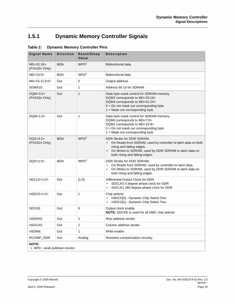
1.5 Signal DescriptionsThis section describes the signals used by the DMC (see Table 2, “Dynamic Memory Controller Pins").
Table 1: PXA3xx Processors Feature Differences
Feature PXA30x PXA31x PXA32x
Maximum Bus Width 16-bits 16-bits 32-bits
SDRAM Clock frequency in S0/D0CS/C0 15 MHz 15 MHz or 30 MHz1 15 MHz or 30 MHz1
Chip Select address space 512 Mbyte 512 Mbyte 1 Gbyte
1. The SDRAM clock frequency is selected using the DDR_D0CS bit in the Application Subsystem Clock Control Register (ACCR).
Dynamic Memory ControllerSignal Descriptions
Copyright © 2009 Marvell Doc. No. MV-S301374-02 Rev. 2.0Version -
April 6, 2009 Released Page 15
12345678910111213141516171819202122232425262728293031323334353637383940414243444546474849505152535455565758
1.5.1 Dynamic Memory Controller Signals
Table 2: Dynamic Memory Controller Pins
Signal Name Direction Reset /SleepValue
Description
MD<31:16> (PXA32x Only)
BiDir WPD1 Bidirectional data
MD<15:0> BiDir WPD1 Bidirectional data
MA<15:11,9:0> Out 0 Output address
SDMA10 Out 1 Address bit 10 for SDRAM
DQM<3:2> (PXA32x Only)
Out 1 Data byte mask control for SDRAM memory.DQM2 corresponds to MD<23:16>DQM3 corresponds to MD<31:24>0 = Do not mask out corresponding byte1 = Mask out corresponding byte
DQM<1:0> Out 1 Data byte mask control for SDRAM memory.DQM0 corresponds to MD<7:0>DQM1 corresponds to MD<15:8>0 = Do not mask out corresponding byte1 = Mask out corresponding byte
DQS<3:2> (PXA32x Only)
BiDir WPD1 DDR Strobe for DDR SDRAM. • On Reads from SDRAM, used by controller to latch data on both
rising and falling edges. • On Writes to SDRAM, used by DDR SDRAM to latch data on
both rising and falling edges.
DQS<1:0> BiDir WPD1 DDR Strobe for DDR SDRAM. • On Reads from SDRAM, used by controller to latch data. • On Writes to SDRAM, used by DDR SDRAM to latch data on
both rising and falling edges.
SDCLK<1:0> Out [1,0] Differential Output Clock for DDR. • SDCLK0 0 degree phase clock for DDR• SDCLK1 180 degree phase clock for DDR
nSDCS<1:0> Out 1 Chip selects • nSDCS[0] - Dynamic Chip Select One• nSDCS[1] - Dynamic Chip Select Two
SDCKE Out 0 Output clock enableNOTE: SDCKE is used for all DMC chip selects.
nSDRAS Out 1 Row address strobe
nSDCAS Out 1 Column address strobe
nSDWE Out 1 Write enable
RCOMP_DDR Out Analog Resistive compensation circuitry
NOTE:1. WPD - weak pulldown resistor.
PXA3xx (88AP3xx) Processor Family Vol. II: Memory Controller Configuration Developers Manual
Doc. No. MV-S301374-02 Rev. 2.0 Version -
Copyright © 2009 Marvell
Page 16 April 6, 2009 Released
12345678910111213141516171819202122232425262728293031323334353637383940414243444546474849505152535455565758
1.6 OperationThis section details the functions of the DMC, phase detector, calibration circuit and resistive compensation.
1.6.1 Dynamic (SDRAM) Controller FunctionsThe DMC handles all DDR SDRAM memory transactions. The SDRAM interface supports 16-bit and 32-bit wide chip selects (partitions) of SDRAM. Each partition is allocated 512 Mbyte (PXA30x and PXA31x) or 1 Gbyte (PXA32x only) of the internal memory map selected by the Section 1.9.2, SDRAM Configuration Register (MDCNFG). However, the physical size of each partition depends on the particular SDRAM type and configuration used, and the MDCNFG[DRAC] and MDCNFG[DCAC] bits. The two SDRAM partitions must have the same timing parameter (tRAS, tRP, tRCD, tRC), the same width (16 bit), and the same frequency.
Note
Note The density for each partition can be a different size.
1.6.1.1 SDRAM RefreshesThe DMC performs auto-refresh (CBR) during normal operation and supports self-refreshing SDRAM during low-power modes in which the dynamic controller clocks and power are shut off. An SDRAM Auto-powerdown mode is used to turn off SDCLK to the DRAM when the DRAM is not being accessed. The SDRAM Refresh Control Register (MDREFR) sets the interval that the DMC sends refresh commands to the DDR SDRAM. After reset (hardware or GPIO), the MDREFR register must be written with the correct refresh interval that meets the DDR SDRAM requirements specified in the device datasheet. Hardware automatically distributes the auto-refresh commands. Consult the DDR SDRAM datasheet for the correct values for MDREFR[DRI].
1.6.1.2 Phase Detector OperationThe phase detector is used to for hardware calibrations of the delay line data strobes (DQSx). The Out of Range interrupt (DMCIER[EORF]) must be enabled to interrupt the processor when the phase detector value is found to be out of range. The phase detector compares the new value with the old value residing in DMCISR[ORV] field. If the new value is found to be out of the range specified by the DDR_HCAL[HCRNG], the new value determined by the phase detector is written to DMCISR[ORV] field. The phase detector does not alter the strobe or the READ command. For more information on enabling the phase detector, refer to Section 1.9.4, DDR Hardware Calibration Register (DDR_HCAL).
1.6.1.3 Delay Line Calibration OperationThe phase detection circuit is used for hardware calibration to determine the number of delay-line elements required to delay the DQSx strobe by ¼ of an SDCLK clock cycle across voltage and temperature variations. DDR strobe calibration and configuration is performed by hardware. Four separate delay lines exist to calibrate the eight possible strobes: 1 strobe / byte = 4 strobes.
Hardware calibration can be configured to interrupt the processor when a new delay-line value is programmed or when the delay-line value falls out of range. If hardware reprograms the delay line, an offset can be set by software and applied to the value determined by the phase detector. A status register, DMCISR, is used to provide interrupt status and the results of the phase-detection circuits.
For more information on the hardware calibration settings, refer to the Section 1.9.4, DDR Hardware Calibration Register (DDR_HCAL) and Section 1.9.5, DDR Write Strobe Calibration Register (DDR_WCAL).

Dynamic Memory ControllerOperation
Copyright © 2009 Marvell Doc. No. MV-S301374-02 Rev. 2.0Version -
April 6, 2009 Released Page 17
12345678910111213141516171819202122232425262728293031323334353637383940414243444546474849505152535455565758
Note
Note The phase detector must be enabled for S0/D0/C0 and is optional for S0/D0CS/C0. Refer to section Section 1.8.5, Power Mode: S0/D0CS/C0 for more information on S0/D0CS/C0 mode.
1.6.1.4 Resistive Compensation (RCOMP)RCOMP dynamically compensates the DMC output drivers to account for variations in operating conditions due to process, temperature, voltage, and board layout. These effects are measured through a resistive mechanism referred to as a Resistive Dynamic Compensation feature, called RCOMP. The DMC interface is designed to work with RCOMP enabled for all operations.
RCOMP tunes four separate output driver parameters:
Pullup strength (PCODE)Pulldown strength (NCODE)Pullup slew rate (PSLEW)
Pulldown slew rate (NSLEW)
These parameters are tuned separately for the groups defined in Table 2. The groups are adjusted using the registers in Section 1.9.9, Programmable Buffer Strength and Slew Registers.
Resistive compensation can be divided into two sub-sequences:
1. RCOMP evaluation: When the conditions of the silicon are sampled and the new RCOMP value is determined.
2. RCOMP update: When the output drivers receive the new PCODE, NCODE, PSLEW, and NSLEW settings.
The RCOMP compensation sequence (evaluation and update) must be performed initially when the processor resets and then periodically afterwards. The initial sequence is initiated directly by software when programming the Section 1.9.8.2, Rcomp Control Register (RCOMP).
Periodic evaluation is based on a programmable RCOMP timer (RCOMP[REI]).For more information on the procedures for setting up and programming the RCOMP circuits refer to 1.8 "Power Mode, Reset and Frequency Changes"
1.6.1.5 Auto Powerdown Mode (APD)Auto-powerdown is an automatic mechanism for minimizing power consumption in the processor. It works by sending the “powerdown” command to SDRAM when no memory transaction requests are
Table 2: RCOMP Strength/Slew Control Groups
Register Descript ion
PAD_MA Strength/Slew Settings for MA[15:0]
PAD_MDMSB Strength/Slew Settings for MD[31:16]
PAD_MDLSB Strength/Slew Settings for MD[15:0], DQM<3:0>, and DQS<3:0>
PAD_DMEM Strength/Slew Settings for nSDCAS, nSDRAS, nSDWE, SDCKE, and SDMA10
PAD_SDCLK Strength/Slew Settings for SDCLK[1:0]
PAD_SDCS Strength/Slew Settings for nSDCS[1:0]
PXA3xx (88AP3xx) Processor Family Vol. II: Memory Controller Configuration Developers Manual
Doc. No. MV-S301374-02 Rev. 2.0 Version -
Copyright © 2009 Marvell
Page 18 April 6, 2009 Released
12345678910111213141516171819202122232425262728293031323334353637383940414243444546474849505152535455565758
queued. This in turn shuts off the SDRAM internal clocking and input receivers, and for SSTL receivers, allows the SSTL Vref to be powered down because SDRAM CKE and CLK pins used to restart the SDRAM can sense LVCMOS levels. For the processor, APD mode is always enabled and cannot be turned off by software.
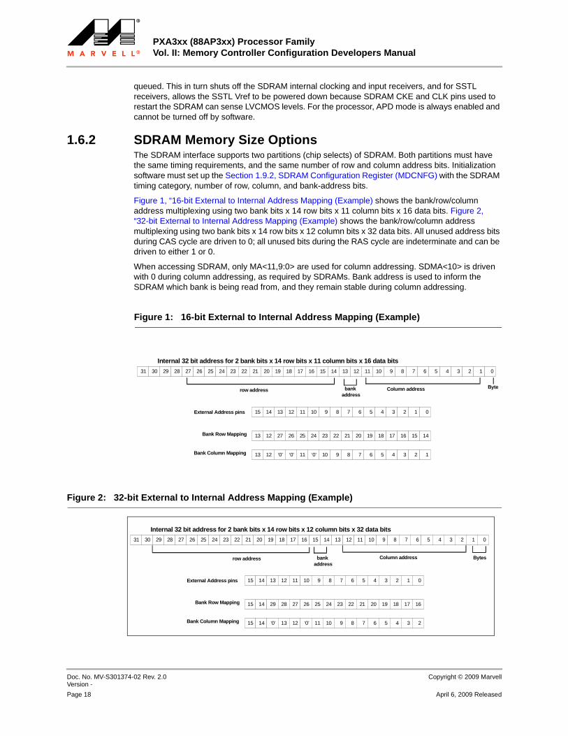
1.6.2 SDRAM Memory Size OptionsThe SDRAM interface supports two partitions (chip selects) of SDRAM. Both partitions must have the same timing requirements, and the same number of row and column address bits. Initialization software must set up the Section 1.9.2, SDRAM Configuration Register (MDCNFG) with the SDRAM timing category, number of row, column, and bank-address bits.
Figure 1, “16-bit External to Internal Address Mapping (Example) shows the bank/row/column address multiplexing using two bank bits x 14 row bits x 11 column bits x 16 data bits. Figure 2, “32-bit External to Internal Address Mapping (Example) shows the bank/row/column address multiplexing using two bank bits x 14 row bits x 12 column bits x 32 data bits. All unused address bits during CAS cycle are driven to 0; all unused bits during the RAS cycle are indeterminate and can be driven to either 1 or 0.
When accessing SDRAM, only MA<11,9:0> are used for column addressing. SDMA<10> is driven with 0 during column addressing, as required by SDRAMs. Bank address is used to inform the SDRAM which bank is being read from, and they remain stable during column addressing.
Figure 1: 16-bit External to Internal Address Mapping (Example)
Byte
31 30 29 28 27 26 25 24 23 22 21 20 19 18 17 16 15 14 13 12 11 10 9 8 7 6 5 4 3 2 1 0
Column addressbank address
row address
15 14 13 12 11 10 9 8 7 6 5 4 3 2 1 0
13 12 27 26 25 24 23 22 21 20 19 18 17 16 15 14
13 12 ‘0’ ‘0’ 11 ‘0’ 10 9 8 7 6 5 4 3 2 1
Bank Row Mapping
Bank Column Mapping
External Address pins
Internal 32 bit address for 2 bank bits x 14 row bits x 11 column bits x 16 data bits
Figure 2: 32-bit External to Internal Address Mapping (Example)
Bytes
31 30 29 28 27 26 25 24 23 22 21 20 19 18 17 16 15 14 13 12 11 10 9 8 7 6 5 4 3 2 1 0
Column addressbank address
row address
15 14 13 12 11 10 9 8 7 6 5 4 3 2 1 0
15 14 29 28 27 26 25 24 23 22 21 20 19 18 17 16
15 14 ‘0’ 13 12 ‘0’ 11 10 9 8 7 6 5 4 3 2
Bank Row Mapping
Bank Column Mapping
External Address pins
Internal 32 bit address for 2 bank bits x 14 row bits x 12 column bits x 32 data bits
Dynamic Memory ControllerOperation
Copyright © 2009 Marvell Doc. No. MV-S301374-02 Rev. 2.0Version -
April 6, 2009 Released Page 19
12345678910111213141516171819202122232425262728293031323334353637383940414243444546474849505152535455565758
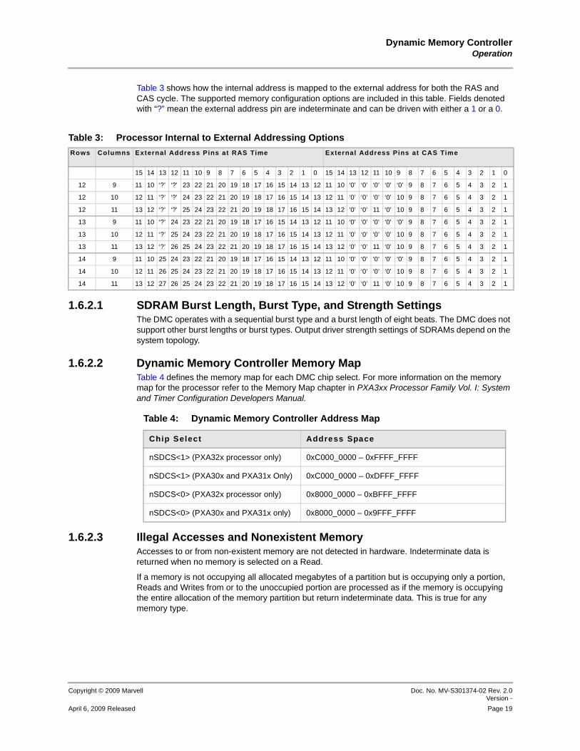
Table 3 shows how the internal address is mapped to the external address for both the RAS and CAS cycle. The supported memory configuration options are included in this table. Fields denoted with “?” mean the external address pin are indeterminate and can be driven with either a 1 or a 0.
1.6.2.1 SDRAM Burst Length, Burst Type, and Strength SettingsThe DMC operates with a sequential burst type and a burst length of eight beats. The DMC does not support other burst lengths or burst types. Output driver strength settings of SDRAMs depend on the system topology.
1.6.2.2 Dynamic Memory Controller Memory MapTable 4 defines the memory map for each DMC chip select. For more information on the memory map for the processor refer to the Memory Map chapter in PXA3xx Processor Family Vol. I: System and Timer Configuration Developers Manual.
1.6.2.3 Illegal Accesses and Nonexistent MemoryAccesses to or from non-existent memory are not detected in hardware. Indeterminate data is returned when no memory is selected on a Read.
If a memory is not occupying all allocated megabytes of a partition but is occupying only a portion, Reads and Writes from or to the unoccupied portion are processed as if the memory is occupying the entire allocation of the memory partition but return indeterminate data. This is true for any memory type.
Table 3: Processor Internal to External Addressing Options
Rows Columns External Address Pins at RAS Time External Address Pins at CAS Time
15 14 13 12 11 10 9 8 7 6 5 4 3 2 1 0 15 14 13 12 11 10 9 8 7 6 5 4 3 2 1 0
12 9 11 10 ‘?’ ‘?’ 23 22 21 20 19 18 17 16 15 14 13 12 11 10 ‘0’ ‘0’ ‘0’ ‘0’ ‘0’ 9 8 7 6 5 4 3 2 1
12 10 12 11 ‘?’ ‘?’ 24 23 22 21 20 19 18 17 16 15 14 13 12 11 ‘0’ ‘0’ ‘0’ ‘0’ 10 9 8 7 6 5 4 3 2 1
12 11 13 12 ‘?’ ‘?’ 25 24 23 22 21 20 19 18 17 16 15 14 13 12 ‘0’ ‘0’ 11 ‘0’ 10 9 8 7 6 5 4 3 2 1
13 9 11 10 ‘?’ 24 23 22 21 20 19 18 17 16 15 14 13 12 11 10 ‘0’ ‘0’ ‘0’ ‘0’ ‘0’ 9 8 7 6 5 4 3 2 1
13 10 12 11 ‘?’ 25 24 23 22 21 20 19 18 17 16 15 14 13 12 11 ‘0’ ‘0’ ‘0’ ‘0’ 10 9 8 7 6 5 4 3 2 1
13 11 13 12 ‘?’ 26 25 24 23 22 21 20 19 18 17 16 15 14 13 12 ‘0’ ‘0’ 11 ‘0’ 10 9 8 7 6 5 4 3 2 1
14 9 11 10 25 24 23 22 21 20 19 18 17 16 15 14 13 12 11 10 ‘0’ ‘0’ ‘0’ ‘0’ ‘0’ 9 8 7 6 5 4 3 2 1
14 10 12 11 26 25 24 23 22 21 20 19 18 17 16 15 14 13 12 11 ‘0’ ‘0’ ‘0’ ‘0’ 10 9 8 7 6 5 4 3 2 1
14 11 13 12 27 26 25 24 23 22 21 20 19 18 17 16 15 14 13 12 ‘0’ ‘0’ 11 ‘0’ 10 9 8 7 6 5 4 3 2 1
Table 4: Dynamic Memory Controller Address Map
Chip Select Address Space
nSDCS<1> (PXA32x processor only) 0xC000_0000 – 0xFFFF_FFFF
nSDCS<1> (PXA30x and PXA31x Only) 0xC000_0000 – 0xDFFF_FFFF
nSDCS<0> (PXA32x processor only) 0x8000_0000 – 0xBFFF_FFFF
nSDCS<0> (PXA30x and PXA31x only) 0x8000_0000 – 0x9FFF_FFFF

PXA3xx (88AP3xx) Processor Family Vol. II: Memory Controller Configuration Developers Manual
Doc. No. MV-S301374-02 Rev. 2.0 Version -
Copyright © 2009 Marvell
Page 20 April 6, 2009 Released
12345678910111213141516171819202122232425262728293031323334353637383940414243444546474849505152535455565758
Note
Note Accesses to reserved memory-controller register space result in indeterminate behavior.
1.6.3 SDRAM Command OverviewWhen writing to the MDMRS register for each enabled SDRAM partition, a Mode Register Set command (MRS) or Extended Mode Register Set command (EMRS) is sent to the SDRAM devices. Whatever is written into the register bits is passed directly to the SDRAMs. Therefore, the software must ensure that the parameters programmed into the SDRAM match those programmed into the configuration registers. During SDRAM configuration, all of the address pins are used to transfer the MRS command.
The processor accesses SDRAM by using the following subset of standard interface commands:
Mode register set (MRS)Extended Mode register set (EMRS)
Bank activate (ACT)Read (READ)Write (WRITE)
Precharge all banks (PALL)Precharge one bank (PRE)Auto-refresh (CBR)
Powerdown (PWRDN)Enter self-refresh (SLFRSH)Exit powerdown (PWRDNX)
No operation (NOP)
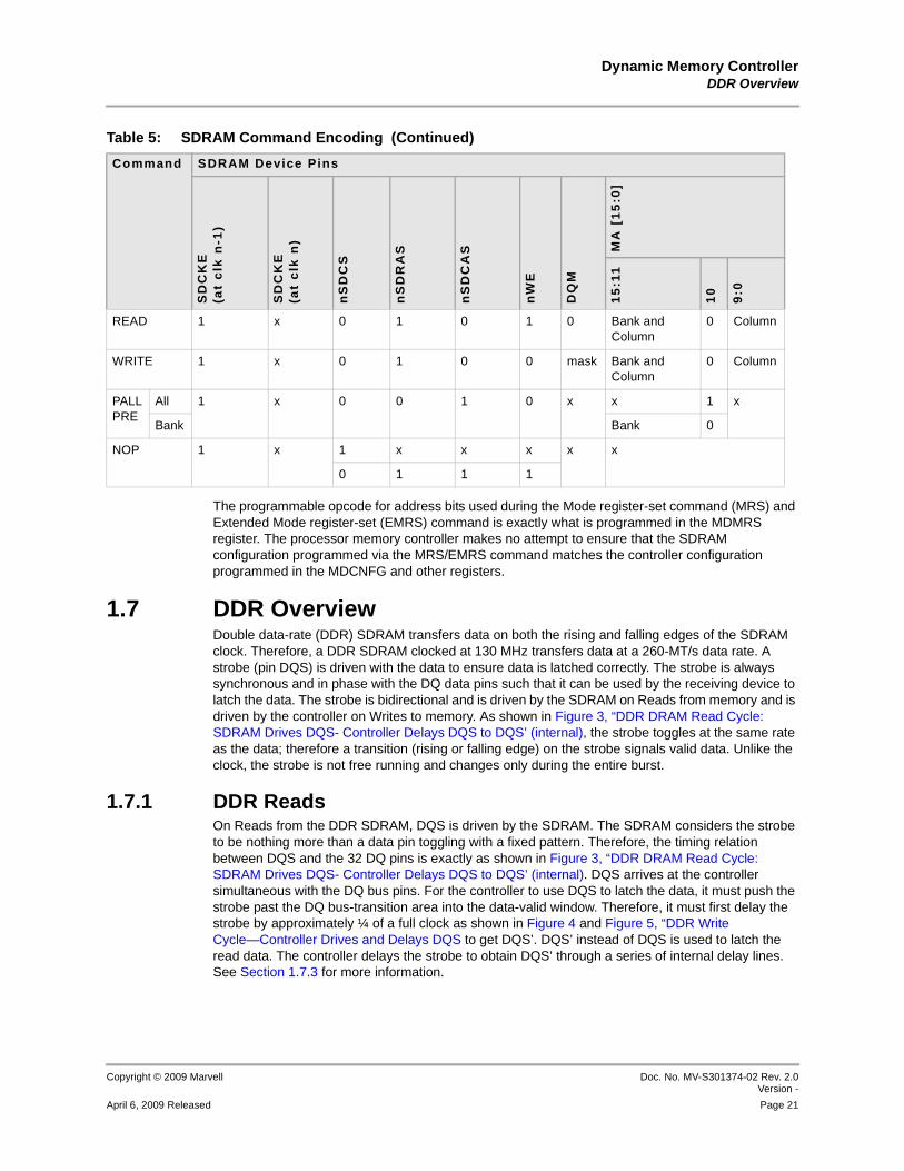
Table 5, “SDRAM Command Encoding" shows the SDRAM interface commands.
Table 5: SDRAM Command Encoding
Command SDRAM Device Pins
SD
CK
E(a
t c
lk n
-1)
SD
CK
E(a
t c
lk n
)
nS
DC
S
nS
DR
AS
nS
DC
AS
nW
E
DQ
M
MA
[1
5:0
]1
5:1
1
10
9:0
PWRDN 1 0 1 1 1 1 1 x
PWRDNX 0 1 1 1 1 1 1 x
SLFRSH 1 0 0 0 0 1 0 x
CBR 1 1 0 0 0 1 x x
MRS/EMRS 1 x 0 0 0 0 1 OP code
ACT 1 x 0 0 1 1 x Bank and Row
Dynamic Memory ControllerDDR Overview
Copyright © 2009 Marvell Doc. No. MV-S301374-02 Rev. 2.0Version -
April 6, 2009 Released Page 21
12345678910111213141516171819202122232425262728293031323334353637383940414243444546474849505152535455565758
The programmable opcode for address bits used during the Mode register-set command (MRS) and Extended Mode register-set (EMRS) command is exactly what is programmed in the MDMRS register. The processor memory controller makes no attempt to ensure that the SDRAM configuration programmed via the MRS/EMRS command matches the controller configuration programmed in the MDCNFG and other registers.
1.7 DDR OverviewDouble data-rate (DDR) SDRAM transfers data on both the rising and falling edges of the SDRAM clock. Therefore, a DDR SDRAM clocked at 130 MHz transfers data at a 260-MT/s data rate. A strobe (pin DQS) is driven with the data to ensure data is latched correctly. The strobe is always synchronous and in phase with the DQ data pins such that it can be used by the receiving device to latch the data. The strobe is bidirectional and is driven by the SDRAM on Reads from memory and is driven by the controller on Writes to memory. As shown in Figure 3, “DDR DRAM Read Cycle: SDRAM Drives DQS- Controller Delays DQS to DQS’ (internal), the strobe toggles at the same rate as the data; therefore a transition (rising or falling edge) on the strobe signals valid data. Unlike the clock, the strobe is not free running and changes only during the entire burst.
1.7.1 DDR ReadsOn Reads from the DDR SDRAM, DQS is driven by the SDRAM. The SDRAM considers the strobe to be nothing more than a data pin toggling with a fixed pattern. Therefore, the timing relation between DQS and the 32 DQ pins is exactly as shown in Figure 3, “DDR DRAM Read Cycle: SDRAM Drives DQS- Controller Delays DQS to DQS’ (internal). DQS arrives at the controller simultaneous with the DQ bus pins. For the controller to use DQS to latch the data, it must push the strobe past the DQ bus-transition area into the data-valid window. Therefore, it must first delay the strobe by approximately ¼ of a full clock as shown in Figure 4 and Figure 5, “DDR Write Cycle—Controller Drives and Delays DQS to get DQS’. DQS’ instead of DQS is used to latch the read data. The controller delays the strobe to obtain DQS’ through a series of internal delay lines. See Section 1.7.3 for more information.
READ 1 x 0 1 0 1 0 Bank andColumn
0 Column
WRITE 1 x 0 1 0 0 mask Bank andColumn
0 Column
PALLPRE
All 1 x 0 0 1 0 x x 1 x
Bank Bank 0
NOP 1 x 1 x x x x x
0 1 1 1
Table 5: SDRAM Command Encoding (Continued)
Command SDRAM Device Pins
SD
CK
E(a
t c
lk n
-1)
SD
CK
E(a
t c
lk n
)
nS
DC
S
nS
DR
AS
nS
DC
AS
nW
E
DQ
M
MA
[1
5:0
]1
5:1
1
10
9:0
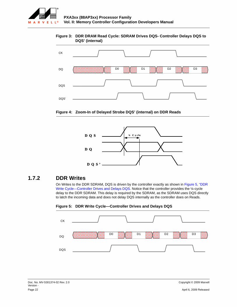
PXA3xx (88AP3xx) Processor Family Vol. II: Memory Controller Configuration Developers Manual
Doc. No. MV-S301374-02 Rev. 2.0 Version -
Copyright © 2009 Marvell
Page 22 April 6, 2009 Released
12345678910111213141516171819202122232425262728293031323334353637383940414243444546474849505152535455565758
Figure 3: DDR DRAM Read Cycle: SDRAM Drives DQS- Controller Delays DQS to DQS’ (internal)
1.7.2 DDR WritesOn Writes to the DDR SDRAM, DQS is driven by the controller exactly as shown in Figure 5, “DDR Write Cycle—Controller Drives and Delays DQS. Notice that the controller provides the ¼-cycle delay to the DDR SDRAM. This delay is required by the SDRAM, as the SDRAM uses DQS directly to latch the incoming data and does not delay DQS internally as the controller does on Reads.
Figure 5: DDR Write Cycle—Controller Drives and Delays DQS
Figure 4: Zoom-In of Delayed Strobe DQS’ (internal) on DDR Reads
CK
DQ
DQS
D0
DQS’
D0 D1 D2 D3
D Q S
D Q
D Q S ’
¼ C y c l eD Q S
D Q
D Q S ’
¼ C y c l e
CK
DQ D0
DQS
D0 D1 D2 D3
Dynamic Memory ControllerPower Mode, Reset and Frequency Changes
Copyright © 2009 Marvell Doc. No. MV-S301374-02 Rev. 2.0Version -
April 6, 2009 Released Page 23
12345678910111213141516171819202122232425262728293031323334353637383940414243444546474849505152535455565758
1.7.3 Strobe Delay Calibration and ProgrammingDDR SDRAM requires a separate strobe (DQS) for each byte of data on the DQ data bus. Therefore, there must be support for the calibration and configuration of two separate delay lines. The delay lines are programmable to account for variations in processor transistor characteristics, operating conditions (voltage and temperature), and system-load characteristics (including board-routing topologies). Voltage (V) and temperature (T) vary while the part is running, periodically monitoring the calibration and reconfiguring the delay into the center of the data-valid window is required. For more information on the procedures for setting up and programming the delay line calibrations, refer to Section 1.8.
Figure 6: Data-Valid Window
Figure 6 shows where the DQ pins are sampled for a given DQS strobe delay:
0–10 strobe-delay elements selected—not enough delay and the Read fails.11–26 strobe-delay elements selected—passing region; ideal delay uses 19 delay elements.> 27 strobe-delay elements—too much delay selected.
1.8 Power Mode, Reset and Frequency Changes This section details the DMC requirements when changing power modes (S0/D1/C2, S0/D2/C2 and S0/D0CS/C0), when a reset occurs (hardware of GPIO), and when changing SDRAM clock frequencies.
1.8.1 SDRAM Reset/Power-Up ProcedureSoftware is responsible for controlling the following procedures when coming out of a hardware reset. Follow the startup procedure exactly, in the order specified, or proper operation cannot be guaranteed.
Note
Note DDR memory accesses are ignored until MDCNFG[DMCEN] is set. If MDCNFG[DMCEN] is cleared, requests will hang.
1. On hardware reset, complete a power-on wait period to allow the internal clocks used to generate SDCLK to stabilize. The JEDEC power-on wait time requirement is 200µs. Refer to the SDRAM datasheet for exact device timing requirements.
2. Program the DTC[1:0], DRAC[1:0], DCAC[1:0] bits in the Section 1.9.2, SDRAM Configuration
Register (MDCNFG) to configure the timing and addressing scheme for the SDRAM device.1,2
0.00 1.50 3.01 4.51 6.02RightLimit
7.52LeftLimit
Middle ofDVW
1 2 3 4 5 6 7 8 9 10 11 12 13 14 15 16 17 18 19 20 21 22 23 24 25 26 27 28 29 30 31 32

PXA3xx (88AP3xx) Processor Family Vol. II: Memory Controller Configuration Developers Manual
Doc. No. MV-S301374-02 Rev. 2.0 Version -
Copyright © 2009 Marvell
Page 24 April 6, 2009 Released
12345678910111213141516171819202122232425262728293031323334353637383940414243444546474849505152535455565758
3. Enable the occupied DRAM partitions by setting appropriate MDCNFG[DCSEx] bits.1 When the partitions are enabled, SDCKE is asserted and SDCLK<1:0> begins to toggle.
4. Wait a typical NOP power-up waiting period required by SDRAM. (Refer to the SDRAM datasheet for exact device timing requirements) Steps 5 and 6 can be executed during this waiting period.
5. Setup the RCOMP interrupt interval and perform an initial RCOMP calibration cycle.1,9
a) Enable the RCOMP interrupt by setting the DMCIER[ERCI] register.b) Program the preferred range into RCOMP[RCRNG]. This is the range in which the new
sample can differ from the old sample before the processor is interrupted.3
c) Program the preferred interval between RCOMP evaluation cycles into RCOMP[REI].4
d) Force an initial RCOMP evaluation phase by setting RCOMP[SWEVAL]. Once the evaluationcycle is complete, this bit clears automatically.5
e) Once the RCOMP interrupt is received, software must use the new values from theDMCISR[PCODE] and DMCISR[NCODE] fields to calculate the NSLEW and PSLEWvalues.
f) Software programs the new NCODE, PCODE, NSLEW and PSLEW into thePAD_XX[NCODE], PAD_XX[PCODE], PAD_XX[NSLEW] and PAD_XX[PSLEW] controlfields.
g) Software must set the RCOMP[UPDATE] bit to force four NOP cycles on the DMC interfaceand to update the output drivers.
h) RCOMP[UPDATE] is cleared automatically by hardware, and normal operation is resumedonce the update is complete.
6. Configure the SDRAM strobe delay calibration1. This step can be performed in parallel with Step 5.
a) Enable the calibration-complete interrupt DMCIER[EDLP].10 b) Clear DDR_HCAL[HCRNG] to guarantee interrupt occurs (if HCRNG is greater than 1, the
interrupt occurs only if out of calibration).c) Clear the DDR_HCAL[HCOFFx] bits6. d) Clear the DDR_WCAL[WCOFF] bit.7
e) Clear the DDR_WCAL[WCEN] so the Write strobe is shifted using the falling edge of theSDCLK.
f) Set DDR_HCAL[HCEN] to enable the phase detector.g) Set the DDR_HCAL[PROG] to enable automatic hardware delay line calibration updates.h) Set the MDCNFG[HWFREQ] bit to enable automatic delay line calibrations during a
frequency change.8
i) The RCOMP cycle completes before delay-line calibration completes. If RCOMP codes mustbe updated, software must do so before proceeding to Step 10.
7. Write the MRS register to condition the SDRAM and send the MRS command. The SDRAM gets “conditioned” by setting MDMRS[MDCOND], before the MRS command MDMRS[13:0] is issued (performed by writing to the MDMRS register once).
8. Program the MDREFR[DRI] register with the required refresh interval.1
9. Program DDR_HCAL[HCRNG] to greater than 1 so that the DMCISR[DLP] interrupt occurs if
out of calibration.1, 11
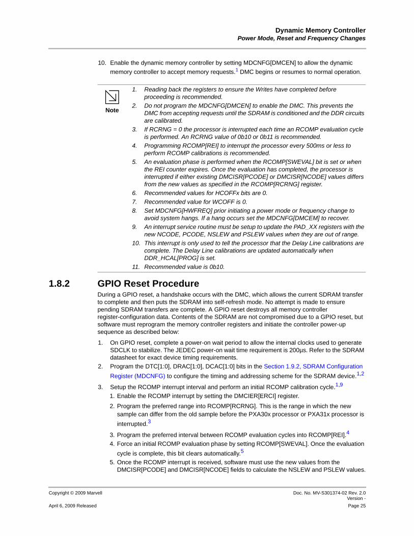
Dynamic Memory ControllerPower Mode, Reset and Frequency Changes
Copyright © 2009 Marvell Doc. No. MV-S301374-02 Rev. 2.0Version -
April 6, 2009 Released Page 25
12345678910111213141516171819202122232425262728293031323334353637383940414243444546474849505152535455565758
10. Enable the dynamic memory controller by setting MDCNFG[DMCEN] to allow the dynamic
memory controller to accept memory requests.1 DMC begins or resumes to normal operation.
1.8.2 GPIO Reset ProcedureDuring a GPIO reset, a handshake occurs with the DMC, which allows the current SDRAM transfer to complete and then puts the SDRAM into self-refresh mode. No attempt is made to ensure pending SDRAM transfers are complete. A GPIO reset destroys all memory controller register-configuration data. Contents of the SDRAM are not compromised due to a GPIO reset, but software must reprogram the memory controller registers and initiate the controller power-up sequence as described below:
1. On GPIO reset, complete a power-on wait period to allow the internal clocks used to generate SDCLK to stabilize. The JEDEC power-on wait time requirement is 200µs. Refer to the SDRAM datasheet for exact device timing requirements.
2. Program the DTC[1:0], DRAC[1:0], DCAC[1:0] bits in the Section 1.9.2, SDRAM Configuration
Register (MDCNFG) to configure the timing and addressing scheme for the SDRAM device.1,2
3. Setup the RCOMP interrupt interval and perform an initial RCOMP calibration cycle.1,9
1. Enable the RCOMP interrupt by setting the DMCIER[ERCI] register.
2. Program the preferred range into RCOMP[RCRNG]. This is the range in which the new sample can differ from the old sample before the PXA30x processor or PXA31x processor is
interrupted.3
3. Program the preferred interval between RCOMP evaluation cycles into RCOMP[REI].4
4. Force an initial RCOMP evaluation phase by setting RCOMP[SWEVAL]. Once the evaluation
cycle is complete, this bit clears automatically.5
5. Once the RCOMP interrupt is received, software must use the new values from the DMCISR[PCODE] and DMCISR[NCODE] fields to calculate the NSLEW and PSLEW values.
Note
1. Reading back the registers to ensure the Writes have completed before proceeding is recommended.
2. Do not program the MDCNFG[DMCEN] to enable the DMC. This prevents the DMC from accepting requests until the SDRAM is conditioned and the DDR circuits are calibrated.
3. If RCRNG = 0 the processor is interrupted each time an RCOMP evaluation cycle is performed. An RCRNG value of 0b10 or 0b11 is recommended.
4. Programming RCOMP[REI] to interrupt the processor every 500ms or less to perform RCOMP calibrations is recommended.
5. An evaluation phase is performed when the RCOMP[SWEVAL] bit is set or when the REI counter expires. Once the evaluation has completed, the processor is interrupted if either existing DMCISR[PCODE] or DMCISR[NCODE] values differs from the new values as specified in the RCOMP[RCRNG] register.
6. Recommended values for HCOFFx bits are 0.
7. Recommended value for WCOFF is 0.8. Set MDCNFG[HWFREQ] prior initiating a power mode or frequency change to
avoid system hangs. If a hang occurs set the MDCNFG[DMCEM] to recover.9. An interrupt service routine must be setup to update the PAD_XX registers with the
new NCODE, PCODE, NSLEW and PSLEW values when they are out of range.10. This interrupt is only used to tell the processor that the Delay Line calibrations are
complete. The Delay Line calibrations are updated automatically when DDR_HCAL[PROG] is set.
11. Recommended value is 0b10.
PXA3xx (88AP3xx) Processor Family Vol. II: Memory Controller Configuration Developers Manual
Doc. No. MV-S301374-02 Rev. 2.0 Version -
Copyright © 2009 Marvell
Page 26 April 6, 2009 Released
12345678910111213141516171819202122232425262728293031323334353637383940414243444546474849505152535455565758
6. Software programs the new NCODE, PCODE, NSLEW and PSLEW into the PAD_XX[NCODE], PAD_XX[PCODE], PAD_XX[NSLEW] and PAD_XX[PSLEW] control fields.
7. Software must set the RCOMP[UPDATE] bit to force four NOP cycles on the DMC interface and to update the output drivers.
8. RCOMP[UPDATE] is cleared automatically by hardware, and normal operation is resumed once the update is complete.
4. Configure the SDRAM strobe delay calibration1. This step can be performed in parallel with Step 5.
1. Enable the calibration-complete interrupt DMCIER[EDLP]10.
2. Clear DDR_HCAL[HCRNG] to guarantee interrupt occurs (if HCRNG is greater than 1, the interrupt occurs only if out of calibration).
3. Clear the DDR_HCAL[HCOFFx] bits6.
4. Clear the DDR_WCAL[WCOFF] bit7. 5. Clear the DDR_WCAL[WCEN] so the Write strobe is shifted using the falling edge of the
SDCLK.6. Set DDR_HCAL[HCEN] to enable the phase detector.7. Set the DDR_HCAL[PROG] to enable automatic hardware delay line calibration updates.
8. Set the MDCNFG[HWFREQ] bit to enable automatic delay line calibrations during a
frequency change8.9. The RCOMP cycle completes before delay-line calibration completes. If RCOMP codes must
be updated, software must do so before proceeding to Step 10.5. Program the MDREFR[DRI] register with the required refresh interval.
6. Program DDR_HCAL[HCRNG] to greater than1 so that the DMCISR[DLP] interrupt occurs if
out of calibration11.
7. Enable the DMC by setting MDCNFG[DMCEN] to allow the dynamic memory controller to accept memory requests. At the same time, set MDCNFG[DCSE] bits to enable SDCLK<1:0> to set SDCKE to take the SDRAM out of self-refresh mode.
Dynamic Memory ControllerPower Mode, Reset and Frequency Changes
Copyright © 2009 Marvell Doc. No. MV-S301374-02 Rev. 2.0Version -
April 6, 2009 Released Page 27
12345678910111213141516171819202122232425262728293031323334353637383940414243444546474849505152535455565758
1.8.3 Power Mode: S0/D1/C2, S0/D2/C2 EntryS0/D1/C2 and S0/D2/C2 entry is controlled through internal handshaking with the Services Power Management Unit (SPMU). The SPMU must first drain all memory traffic from the switch interface before initiating S0/D1/C2 or S0/D2/C2 entry request to the DMC.
The DMC performs the following when a request for S0/D1/C2 or S0/D2/C2 is received:
Allows all pending DMC requests to complete
Ensures refresh, RCOMP, and Delay Line calibration requests are completePuts DDR SDRAM into Self-Refresh mode to preserve memory contents.
1.8.4 Power Mode: S0/D1/C2, S0/D2/C2 Exit1. Disable hardware calibration by clearing DDR_HCAL[HCEN] to reset the phase detector
counters, which ensures clean calibration cycle when restarted.
2. Initiate an RCOMP cycle by setting RCOMP[SWEVAL].3. Delay lines must be recalibrated before memory requests can begin. Steps 3c through 3e are
completed at same time. a) Set DMCISR[DLP] to clear the Delay Lines Programmed interrupt status bit.b) Set DMCIER[EDLP] to enable interrupt.c) Set DDR_HCAL[HCEN] to enable phase detector.d) Set DDR_HCAL[PROG] to enable programming of delay lines.e) Clear DDR_HCAL[HCRNG] to guarantee interrupt occurs regardless (if HCRNG is greater
than 1 the interrupt occurs only if out of calibration). Software is interrupted when calibration is complete (512 clk cycles * 1/130 MHz) = 3.94 μSat 130 MHz. This step can be performed in parallel with step 2. The Rcomp cycle completes
Note
1. Reading back the registers to ensure the Writes have completed before proceeding is recommended.
2. Do not program the MDCNFG[DMCEN] or MDCNFG[DCSEx] bits. This prevents the DMC from accepting requests until the SDRAM is conditioned and the DDR circuits are calibrated, and leaves the SDRAM in self-refresh mode.
3. If RCRNG = 0 the processor is interrupted each time an RCOMP evaluation cycle is performed. An RCRNG value of 0b10 or 0b11 is recommended.
4. Programming RCOMP[REI] to interrupt the processor every 500ms or less to perform RCOMP calibrations is recommended.
5. An evaluation phase is performed when the RCOMP[SWEVAL] bit is set or when the REI counter expires. Once the evaluation has completed, the processor is interrupted if either existing DMCISR[PCODE] or DMCISR[NCODE] values differs from the new values as specified in the RCOMP[RCRNG] register.
6. Recommended values for HCOFFx bits are 0.
7. Recommended value for WCOFF is 0.8. Set MDCNFG[HWFREQ] prior initiating a power mode or frequency change to
avoid system hangs. If a hang occurs set the MDCNFG[DMCEM] to recover.9. An interrupt service routine must be setup to update the PAD_XX registers with the
new NCODE, PCODE, NSLEW and PSLEW values when they are out of range.10. This interrupt is only used to tell the processor that the Delay Line calibrations are
complete. The Delay Line calibrations are updated automatically when DDR_HCAL[PROG] is set.
11. Recommended value is 0b10.

PXA3xx (88AP3xx) Processor Family Vol. II: Memory Controller Configuration Developers Manual
Doc. No. MV-S301374-02 Rev. 2.0 Version -
Copyright © 2009 Marvell
Page 28 April 6, 2009 Released
12345678910111213141516171819202122232425262728293031323334353637383940414243444546474849505152535455565758
before delay-line calibration completes. If necessary, software should update Rcomp codesbefore proceeding to step 4.
4. Re-enable the DMC by setting MDCNG[DMCEN].5. Set DDR_HCAL[HCRNG] to greater than 1 so that the DMCISR[DLP] interrupt occurs if out of
calibration. 6. Clear DMCISR[DLP] interrupt status bit.
1.8.5 Power Mode: S0/D0CS/C0 Currently, frequency change is supported only after reset and D0CS mode entry/exit. SDRAM frequency throttling to save power is not supported.
1.8.5.1 Exiting S0/D0CS/C0Delay lines must be calibrated at the new SDRAM frequency before memory accesses occur. The following procedures must be followed:
1. Set DDR_HCAL[HCEN] to enable the phase detector.
2. Read back DDR_HCAL[HCEN] to ensure it is set before proceeding. 3. Set MDCNFG[HWFREQ].
4. Read back MDCNFG[HWFREQ] to ensure it is set before proceeding.
5. When frequency change is complete and delay lines have been calibrated, the controller automatically begins processing memory transactions if the controller and memory have been initialized previously.
1.8.5.2 Entering S0/D0CS/C0Delay lines do not need to be recalibrated when the SDRAM clock frequency is lowered. By omitting delay-line calibration approximately 3.94μs (512 clk cycles * 1/130 MHz) can be saved by disabling the phase detector before initiating change. The following procedures must be followed when calibrating delay lines:
1. Clear DDR_HCAL[HCEN] to disable the phase detector.
2. Read back DDR_HCAL[HCEN] to ensure it is cleared before proceeding. 3. Set MDCNFG[HWFREQ].
4. Read back MDCNFG[DWFREQ] to ensure it is set before proceeding.
5. When frequency change is complete, the controller automatically begins processing memory transactions if the controller and memory have been initialized previously.
Note
Note 1. Set MDCNFG[HWFREQ] prior initiating a power mode or frequency change to avoid system hangs. If a hang occurs, set the MDCNFG[DMCEM] to recover.
2. MDCNFG[HWFREQ] is cleared automatically.
1.9 Register DescriptionsThe section describes in detail the Dynamic Memory Controller configuration registers and the programmable Buffer Strength and Slew registers.
The DMC receives its configuration from the system bus and its memory requests from the switch. These registers are not configured to any particular DMC request. To ensure that a new
Dynamic Memory ControllerRegister Descriptions
Copyright © 2009 Marvell Doc. No. MV-S301374-02 Rev. 2.0Version -
April 6, 2009 Released Page 29
12345678910111213141516171819202122232425262728293031323334353637383940414243444546474849505152535455565758
configuration does not get applied to the wrong memory request, observe the following rules when programming the configuration registers:
Program the MDCNFG, MDMRS, and EMPI registers only after a reset or standby event that results in corruption of configuration data.All other DMC registers can be calibrated “on the fly” because they do not need to be applied to any particular DMC request.
1.9.1 Register SummaryTable 6 shows the registers associated with the DMC interface and the physical addresses used to access them. These registers must be mapped as non-cacheable and non-bufferable and can be accessed only as word accesses.
Table 6: Dynamic Memory Controller Register Summary
Address Descript ion Page
Dynamic Memory Controller Registers
0x4810_0000 SDRAM Configuration Register (MDCNFG) page 30
0x4810_0004 SDRAM Refresh Control Register (MDREFR) page 32
0x4810_0020 reserved
0x4810_0040 SDRAM Mode Register Set Configuration Register (MDMRS)
page 33
0x4810_0050 reserved
0x4810_0060 DDR Hardware Calibration Register (DDR_HCAL) page 34
0x4810_0068 DDR Write Strobe Calibration Register (DDR_WCAL) page 36
0x4810_0070 Dynamic Memory Controller Interrupt Enable Register (DMCIER)
page 37
0x4810_0078 Dynamic Memory Controller Interrupt Status Register (DMCISR)
page 38
0x4810_0080 Delay Line Status Register (DDR_DLS) page 39
0x4810_0090 External Memory Pin Interface Control Register (EMPI)
page 40
0x4810_0100 Rcomp Control Register (RCOMP) page 42
Programmable Buffer Strength and Slew Registers
0x4810_0110 PAD_MA Strength and Slew Settings Register (PAD_MA)
page 43
0x4810_0114 PAD_MDMSB Strength and Slew Settings Register (PAD_MDMSB) (PXA32x processor only) page 44
0x4810_0118 PAD_MDLSB Strength and Slew Settings Register (PAD_MDLSB)
page 45
0x4810_011C PAD_SDRAM Strength and Slew Settings Register (PAD_SDRAM)
page 46
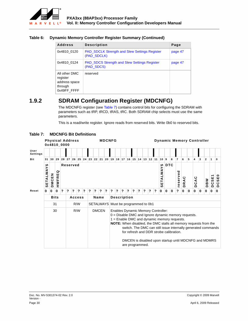
PXA3xx (88AP3xx) Processor Family Vol. II: Memory Controller Configuration Developers Manual
Doc. No. MV-S301374-02 Rev. 2.0 Version -
Copyright © 2009 Marvell
Page 30 April 6, 2009 Released
12345678910111213141516171819202122232425262728293031323334353637383940414243444546474849505152535455565758
1.9.2 SDRAM Configuration Register (MDCNFG)The MDCNFG register (see Table 7) contains control bits for configuring the SDRAM with parameters such as tRP, tRCD, tRAS, tRC. Both SDRAM chip selects must use the same parameters.
This is a read/write register. Ignore reads from reserved bits. Write 0b0 to reserved bits.
0x4810_0120 PAD_SDCLK Strength and Slew Settings Register (PAD_SDCLK)
page 47
0x4810_0124 PAD_SDCS Strength and Slew Settings Register (PAD_SDCS)
page 47
All other DMC register address space through0x49FF_FFFF
reserved
Table 6: Dynamic Memory Controller Register Summary (Continued)
Address Descript ion Page
Table 7: MDCNFG Bit Definitions
Physical Address0x4810_0000
MDCNFG Dynamic Memory Controller
User Settings
Bit 31 30 29 28 27 26 25 24 23 22 21 20 19 18 17 16 15 14 13 12 11 10 9 8 7 6 5 4 3 2 1 0
SE
TA
LW
AY
S
DM
CE
N
HW
FR
EQ
ReservedS
ET
AL
WA
YS DTC
res
erv
ed
DR
AC
DC
AC
DB
W
DC
SE
1
DC
SE
0
Reset 0 0 0 ? ? ? ? ? ? ? ? ? ? ? ? ? ? ? ? ? ? 0 0 0 ? 0 0 0 0 0 0 0
Bits Access Name Descript ion
31 R/W SETALWAYS Must be programmed to 0b1
30 R/W DMCEN Enables Dynamic Memory Controller:0 = Disable DMC and Ignore dynamic memory requests.1 = Enable DMC and dynamic memory requests.NOTE: When disabled, the DMC stalls all memory requests from the
switch. The DMC can still issue internally generated commands for refresh and DDR strobe calibration.
DMCEN is disabled upon startup until MDCNFG and MDMRS are programmed.
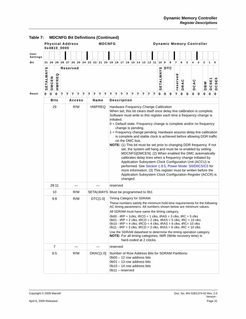
Dynamic Memory ControllerRegister Descriptions
Copyright © 2009 Marvell Doc. No. MV-S301374-02 Rev. 2.0Version -
April 6, 2009 Released Page 31
12345678910111213141516171819202122232425262728293031323334353637383940414243444546474849505152535455565758
29 R/W HWFREQ Hardware Frequency Change CalibrationWhen set, this bit clears itself once delay line calibration is complete. Software must write to this register each time a frequency change is initiated.0 = Default state. Frequency change is complete and/or no frequency
change is pending.1 = Frequency change pending. Hardware assures delay line calibration
is complete and stable clock is achieved before allowing DDR traffic on the DMC bus.
NOTE: (1) This bit must be set prior to changing DDR frequency. If not set, the system will hang and must be re-enabled by setting MDCNFG[DMCEN]. (2) When enabled the DMC automatically calibrates delay lines when a frequency change initiated by Application Subsystem Clock Configuration Unit (ACCU) is performed. See Section 1.8.5, Power Mode: S0/D0CS/C0 for more information. (3) This register must be written before the Application Subsystem Clock Configuration Register (ACCR) is changed.
28:11 — — reserved
10 R/W SETALWAYS Must be programmed to 0b1
9:8 R/W DTC[1:0] Timing Category for SDRAM:
These numbers satisfy the minimum hold time requirements for the following AC timing parameters. All numbers shown below are minimum values.
All SDRAM must have same the timing category.
0b00 - tRP = 1clks, tRCD = 1 clks, tRAS = 3 clks, tRC = 5 clks0b01 - tRP = 2 clks, tRCD = 2 clks, tRAS = 5 clks, tRC = 10 clks0b10 - tRP = 4 clks, tRCD = 4 clks, tRAS = 6 clks, tRC= 10 clks0b11 - tRP = 3 clks, tRCD = 3 clks, tRAS = 6 clks, tRC = 10 clks
Use the SDRAM datasheet to determine the timing operation category.NOTE: For all timing categories, tWR (Write recovery time) is
hard-coded at 2 clocks.
7 — — reserved
6:5 R/W DRAC[1:0] Number of Row Address Bits for SDRAM Partitions:0b00 – 12 row address bits0b01 – 13 row address bits0b10 – 14 row address bits0b11 – reserved
Table 7: MDCNFG Bit Definitions (Continued)
Physical Address0x4810_0000
MDCNFG Dynamic Memory Controller
User Settings
Bit 31 30 29 28 27 26 25 24 23 22 21 20 19 18 17 16 15 14 13 12 11 10 9 8 7 6 5 4 3 2 1 0
SE
TA
LW
AY
S
DM
CE
N
HW
FR
EQ
Reserved
SE
TA
LW
AY
S DTC
res
erv
ed
DR
AC
DC
AC
DB
W
DC
SE
1
DC
SE
0
Reset 0 0 0 ? ? ? ? ? ? ? ? ? ? ? ? ? ? ? ? ? ? 0 0 0 ? 0 0 0 0 0 0 0
Bits Access Name Descript ion
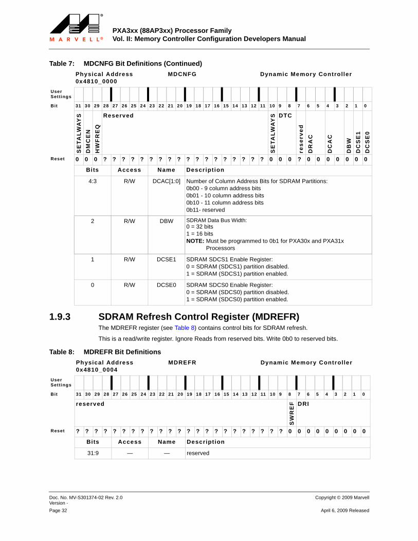
PXA3xx (88AP3xx) Processor Family Vol. II: Memory Controller Configuration Developers Manual
Doc. No. MV-S301374-02 Rev. 2.0 Version -
Copyright © 2009 Marvell
Page 32 April 6, 2009 Released
12345678910111213141516171819202122232425262728293031323334353637383940414243444546474849505152535455565758
1.9.3 SDRAM Refresh Control Register (MDREFR)The MDREFR register (see Table 8) contains control bits for SDRAM refresh.
This is a read/write register. Ignore Reads from reserved bits. Write 0b0 to reserved bits.
4:3 R/W DCAC[1:0] Number of Column Address Bits for SDRAM Partitions:0b00 - 9 column address bits0b01 - 10 column address bits0b10 - 11 column address bits0b11- reserved
2 R/W DBW SDRAM Data Bus Width:0 = 32 bits1 = 16 bitsNOTE: Must be programmed to 0b1 for PXA30x and PXA31x
Processors
1 R/W DCSE1 SDRAM SDCS1 Enable Register:0 = SDRAM (SDCS1) partition disabled.1 = SDRAM (SDCS1) partition enabled.
0 R/W DCSE0 SDRAM SDCS0 Enable Register:0 = SDRAM (SDCS0) partition disabled.1 = SDRAM (SDCS0) partition enabled.
Table 7: MDCNFG Bit Definitions (Continued)
Physical Address0x4810_0000
MDCNFG Dynamic Memory Controller
User Settings
Bit 31 30 29 28 27 26 25 24 23 22 21 20 19 18 17 16 15 14 13 12 11 10 9 8 7 6 5 4 3 2 1 0
SE
TA
LW
AY
S
DM
CE
N
HW
FR
EQ
Reserved
SE
TA
LW
AY
S DTC
res
erv
ed
DR
AC
DC
AC
DB
W
DC
SE
1
DC
SE
0
Reset 0 0 0 ? ? ? ? ? ? ? ? ? ? ? ? ? ? ? ? ? ? 0 0 0 ? 0 0 0 0 0 0 0
Bits Access Name Descript ion
Table 8: MDREFR Bit Definitions
Physical Address0x4810_0004
MDREFR Dynamic Memory Control ler
User Settings
Bit 31 30 29 28 27 26 25 24 23 22 21 20 19 18 17 16 15 14 13 12 11 10 9 8 7 6 5 4 3 2 1 0
reserved
SW
RE
F DRI
Reset ? ? ? ? ? ? ? ? ? ? ? ? ? ? ? ? ? ? ? ? ? ? ? 0 0 0 0 0 0 0 0 0
Bits Access Name Descript ion
31:9 — — reserved

Dynamic Memory ControllerRegister Descriptions
Copyright © 2009 Marvell Doc. No. MV-S301374-02 Rev. 2.0Version -
April 6, 2009 Released Page 33
12345678910111213141516171819202122232425262728293031323334353637383940414243444546474849505152535455565758
1.9.3.1 SDRAM Mode Register Set Configuration Register (MDMRS)The MDMRS register (Table 9) is used to issue MRS and EMRS commands to SDRAM (see Table 5, “SDRAM Command Encoding"). Writing this register triggers a MRS or EMRS command being issued to external SDRAM. The MRS command is written out on MA<15:11>, SDMA10, and MA<9:0> pins.
8 R/W SWREF Software Refresh:0 = No refresh being performed1 = Refresh is performed by the DMC. NOTE: This bit is cleared automatically once the refresh has been
performed.
7:0 R/W DRI<7:0> SDRAM Refresh Interval, All Partitions:The number of refresh clock cycles (divided by 4) between auto-refresh (CBR) cycles. One row is refreshed in each SDRAM bank during each CBR refresh cycle. This interval is applicable to all SDRAM chip selects. The value that must be loaded into this register is calculated as follows: DRI = (Number of refresh clock cycles) / 4
= ((Refresh time / rows) x Refresh clock frequency) / 4. NOTE: (1) This number must be less than the tRAS (max) for the
SDRAM being accessed.(2) The refresh clock is a separate 13MHz clock used only to count refresh, DDR calibration, and RCOMP intervals.(3) DRI values less than 0x14 are not supported. This value should not be programmed less than required, otherwise the performance of the memory controller suffers. When set to 0, no refreshes are sent to the SDRAMs
Table 8: MDREFR Bit Definitions (Continued)
Physical Address0x4810_0004
MDREFR Dynamic Memory Control ler
User Settings
Bit 31 30 29 28 27 26 25 24 23 22 21 20 19 18 17 16 15 14 13 12 11 10 9 8 7 6 5 4 3 2 1 0
reserved
SW
RE
F DRI
Reset ? ? ? ? ? ? ? ? ? ? ? ? ? ? ? ? ? ? ? ? ? ? ? 0 0 0 0 0 0 0 0 0
Bits Access Name Descript ion
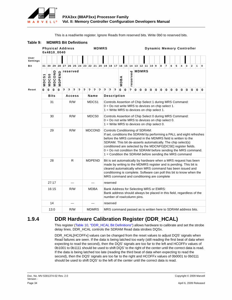
PXA3xx (88AP3xx) Processor Family Vol. II: Memory Controller Configuration Developers Manual
Doc. No. MV-S301374-02 Rev. 2.0 Version -
Copyright © 2009 Marvell
Page 34 April 6, 2009 Released
12345678910111213141516171819202122232425262728293031323334353637383940414243444546474849505152535455565758
This is a read/write register. Ignore Reads from reserved bits. Write 0b0 to reserved bits.
1.9.4 DDR Hardware Calibration Register (DDR_HCAL)This register (Table 10, “DDR_HCAL Bit Definitions") allows hardware to calibrate and set the strobe delay lines. DDR_HCAL controls the SDRAM Read data strobes DQSx.
DDR_HCAL[HCOFFx] values can be changed from the reset values to adjust DQS’ signals when Read failures are seen. If the data is being latched too early (still reading the first beat of data when expecting to read the second), then the DQS’ signals are too far to the left and HCOFFx values of 0b1001 to 0b1111 should be used to shift DQS’ to the right of the center until the correct data is read. If the data is being latched too late (reading the third beat of data when expecting to read the second), then the DQS’ signals are too far to the right and HCOFFx values of 0b0001 to 0b0111 should be used to shift DQS’ to the left of the center until the correct data is read.
Table 9: MDMRS Bit Definitions
Physical Address0x4810_0040
MDMRS Dynamic Memory Control ler
User Settings
Bit 31 30 29 28 27 26 25 24 23 22 21 20 19 18 17 16 15 14 13 12 11 10 9 8 7 6 5 4 3 2 1 0
MD
CS
1
MD
CS
0
MD
CO
ND
MD
PE
ND reserved
MD
BA
res
erv
ed MDMRS
Reset 0 0 0 0 ? ? ? ? ? ? ? ? ? ? ? 0 0 ? 0 0 0 0 0 0 0 0 0 0 0 0 0 0
Bits Access Name Descript ion
31 R/W MDCS1 Controls Assertion of Chip Select 1 during MRS Command:0 = Do not write MRS to devices on chip select 1.1 = Write MRS to devices on chip select 1.
30 R/W MDCS0 Controls Assertion of Chip Select 0 during MRS Command:0 = Do not write MRS to devices on chip select 0.1 = Write MRS to devices on chip select 0.
29 R/W MDCOND Controls Conditioning of SDRAM:If set, conditions the SDRAM by performing a PALL and eight refreshes before the MRS command in the MDMRS field is written to the SDRAM. This bit de-asserts automatically. The chip select(s) conditioned are selected by the MDCNFG[DCSE] register fields.0 = Do not condition the SDRAM before sending the MRS command.1 = Condition the SDRAM before sending the MRS command
28 R MDPEND Bit is set automatically by hardware when a MRS request has been made by writing to the MDMRS register and is pending. This bit is cleared automatically when MRS command has been issued and conditioning is complete. Software can poll this bit to know when the MRS command and conditioning are complete
27:17 — — reserved
16:15 R/W MDBA Bank Address for Selecting MRS or EMRS:Bank address should always be placed in this field, regardless of the number of row/column pins.
14 — — reserved
13:0 R/W MDMRS MRS command passed as is written here to SDRAM address bits.
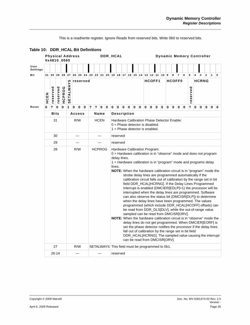
Dynamic Memory ControllerRegister Descriptions
Copyright © 2009 Marvell Doc. No. MV-S301374-02 Rev. 2.0Version -
April 6, 2009 Released Page 35
12345678910111213141516171819202122232425262728293031323334353637383940414243444546474849505152535455565758
This is a read/write register. Ignore Reads from reserved bits. Write 0b0 to reserved bits.
Table 10: DDR_HCAL Bit Definitions
Physical Address0x4810_0060
DDR_HCAL Dynamic Memory Controller
User Settings
Bit 31 30 29 28 27 26 25 24 23 22 21 20 19 18 17 16 15 14 13 12 11 10 9 8 7 6 5 4 3 2 1 0
HC
EN
res
erv
ed
res
erv
ed
HC
PR
OG
SE
TA
LW
AY
S reserved HCOFF1 HCOFF0
res
erv
ed
HCRNG
Reset 0 ? 0 0 1 0 0 0 ? ? 0 0 0 0 0 0 0 0 0 0 0 0 0 0 0 0 ? 0 0 0 0 0
Bits Access Name Descript ion
31 R/W HCEN Hardware Calibration Phase Detector Enable:0 = Phase detector is disabled.1 = Phase detector is enabled.
30 — — reserved
29 — — reserved
28 R/W HCPROG Hardware Calibration Program:0 = Hardware calibration is in “observe” mode and does not program delay lines.1 = Hardware calibration is in “program” mode and programs delay lines.NOTE: When the hardware calibration circuit is in “program” mode the
strobe delay lines are programmed automatically if the calibration circuit falls out of calibration by the range set in bit field DDR_HCAL[HCRNG]. If the Delay Lines Programmed Interrupt is enabled (DMCIER[EDLP]=1) the processor will be interrupted when the delay lines are programmed. Software can also observe the status bit (DMCISR[DLP]) to determine when the delay lines have been programmed. The values programmed (which include DDR_HCAL[HCOFF] offsets) can be read from DDR_DLS[DLV], while the out-of-range value sampled can be read from DMCISR[ORV].
NOTE: When the hardware calibration circuit is in “observe” mode the delay lines do not get programmed. When DMCIER[EORF] is set the phase detector notifies the processor if the delay lines fall out of calibration by the range set in bit field DDR_HCAL[HCRNG]. The sampled value causing the interrupt can be read from DMCISR[ORV].
27 R/W SETALWAYS This field must be programmed to 0b1.
26:14 — — reserved

PXA3xx (88AP3xx) Processor Family Vol. II: Memory Controller Configuration Developers Manual
Doc. No. MV-S301374-02 Rev. 2.0 Version -
Copyright © 2009 Marvell
Page 36 April 6, 2009 Released
12345678910111213141516171819202122232425262728293031323334353637383940414243444546474849505152535455565758
1.9.5 DDR Write Strobe Calibration Register (DDR_WCAL)This register (Table 11, “DDR_WCAL Bit Definitions") lets hardware calibration set the write-strobe delay lines. DDR_WCAL controls external-memory bus strobes DQSx. If DDR_WCAL[WCEN] is clear, Write strobes are calibrated automatically. This is the preferred default mode, but can be overridden using this register. If DDR_WCAL[WCEN] is set, this mode is controlled by the fields described within this register and the DDR_HCAL register.
The method used to calibrate the Write-strobe delay lines is set by the DDR_HCAL register. Several of the fields in these registers are shared by both the Read and Write delay lines, specifically: DDR_HCAL[HCEN], DDR_HCAL[HCPROG], DDR_HCAL[HCRNG]. The Write delay lines have an independent offset defined in the DDR_WCAL[WCOFF]register. Unlike the Read strobes that can be programmed independently, all Write strobes are always programmed with the same values, which is why there is only one DDR_WCAL[WCOFF] field and only one DDR_WCAL[WSDLV] field.
13:10 R/W HCOFF1 Hardware Calibration Offset for DQS[1]:Provides a fractional offset from the value determined by the hardware calibration circuit. The offset range is 1/8 to 15/8 of a DDR data eye. The value programmed into delay line is DQS[1] = (DDR_DMCISR[ORV]) * HCOFF1. 0b0000 = 0 - No offset (strobe centered)0b0001 to 0b0111= 1/8 to 7/8 - Offset (moves strobe left of center)0b1000 = 8/8 - No offset (strobe centered)0b1001 to 0b1111 = 9/8 to 15/8 - Offset (moves strobe right of center)
9:6 R/W HCOFF0 Hardware Calibration Offset for DQS[0]:Provides a fractional offset from the value determined by the hardware calibration circuit. The offset range is 1/8 to 15/8 of a DDR data eye. The value programmed into delay line is DQS[0] = (DDR_DMCISR[ORV]) * HCOFF0.0b0000 = 0 - No offset (strobe centered)0b0001 to 0b0111= 1/8 to 7/8 - Offset (moves strobe left of center)0b1000 = 8/8 - No offset (strobe centered)0b1001 to 0b1111 = 9/8 to 15/8 - Offset (moves strobe right of center)
5 — — reserved
4:0 R/W HCRNG Hardware Calibration Range:Provides a calibration range around DMCISR[ORV]. The new delay value determined by the phase detector is considered to be out of range if one of the following is true.DMCISR[PDV] ≥ DMCISR[ORV] + HCRNGDMCISR[PDV] ≤ DMCISR[ORV] – HCRNG
Table 10: DDR_HCAL Bit Definitions (Continued)
Physical Address0x4810_0060
DDR_HCAL Dynamic Memory Controller
User Settings
Bit 31 30 29 28 27 26 25 24 23 22 21 20 19 18 17 16 15 14 13 12 11 10 9 8 7 6 5 4 3 2 1 0
HC
EN
res
erv
ed
res
erv
ed
HC
PR
OG
SE
TA
LW
AY
S reserved HCOFF1 HCOFF0
res
erv
ed
HCRNG
Reset 0 ? 0 0 1 0 0 0 ? ? 0 0 0 0 0 0 0 0 0 0 0 0 0 0 0 0 ? 0 0 0 0 0
Bits Access Name Descript ion

Dynamic Memory ControllerRegister Descriptions
Copyright © 2009 Marvell Doc. No. MV-S301374-02 Rev. 2.0Version -
April 6, 2009 Released Page 37
12345678910111213141516171819202122232425262728293031323334353637383940414243444546474849505152535455565758
This is a read/write register. Ignore Reads from reserved bits. Write 0b0 to reserved bits.
1.9.6 Dynamic Memory Controller Interrupt Enable Register (DMCIER)The DMCIER is the Interrupt Enable register (Table 12, “DMCIER Bit Definitions") for all of the DMC interrupts. The status bit corresponding to an interrupt is set in the DMCISR register regardless of the enable bit state.
This is a read/write register. Ignore Reads from reserved bits. Write 0b0 to reserved bits.
Table 11: DDR_WCAL Bit Definitions
Physical Address0x4810_0068
DDR_WCAL Dynamic Memory Controller
User Settings
Bit 31 30 29 28 27 26 25 24 23 22 21 20 19 18 17 16 15 14 13 12 11 10 9 8 7 6 5 4 3 2 1 0
WC
EN reserved WSDLV_STATUS reserved WCOFF reserved
Reset 0 ? ? ? ? ? ? ? ? 0 0 0 0 0 0 0 ? ? ? ? 0 0 0 0 ? ? ? ? ? ? ? ?
Bits Access Name Description
31 R/W WCEN Write Calibration Enable:When set, the write strobe is delayed using delay lines instead of the falling clock edge. When set, the write strobe delay line mode is controlled by the fields in this register as well as the DDR_HCAL register.0 = Default mode: Strobe shifted using falling edge of clock.1 = Strobe shifted using delay lines. Mode controlled by DDR_HCAL register.
30:23 — — reserved
22:16 R WSDLVSTATUS
Write Strobe Delay Line Value Status (Read Only):Actual delay line value set by hardware for both DQS write strobes. This value includes WCOFF offset. This field is similar to the read_strobe DDR_DLS[SSDLVx] fields.
15:12 — — reserved
11:8 R/W WCOFF Write Strobe Offset:This field is enabled only when hardware calibration is enabled by setting DDR_HCAL[HCEN]. Provides a fractional offset from the value determined by the hardware calibration circuit. The offset range is 1/8 to 15/8. The value programmed into the delay line is DQS[0] = (DDR_DMCISR[ORV]) * WCOFF. For a derivation of this formula, see Section 1.7.3. This field is similar to Read strobe DDR_HCAL[HCOFF] field.
0b0000 = 0 - No offset (strobe centered) 0b0001 - 0b0111 = 1/8 to 7/8 - Offset (moves strobe left of center) 0b1000 = 8/8 - No offset (strobe centered) 0b1001 - 0b1111 = 9/8 to 15/8 - Offset (moves strobe right of center)
7:0 — — reserved

PXA3xx (88AP3xx) Processor Family Vol. II: Memory Controller Configuration Developers Manual
Doc. No. MV-S301374-02 Rev. 2.0 Version -
Copyright © 2009 Marvell
Page 38 April 6, 2009 Released
12345678910111213141516171819202122232425262728293031323334353637383940414243444546474849505152535455565758
1.9.7 Dynamic Memory Controller Interrupt Status Register (DMCISR)The DMCISR is the Interrupt Status register (see Table 13) for all of the DMC interrupts.
This is a read/write register. Ignore Reads from reserved bits. Write 0b0 to reserved bits.
Table 12: DMCIER Bit Definitions
Physical Address0x4810_0070
DMCIER Dynamic Memory Controller
User Settings
Bit 31 30 29 28 27 26 25 24 23 22 21 20 19 18 17 16 15 14 13 12 11 10 9 8 7 6 5 4 3 2 1 0
ER
CI
EO
RF
ED
LP reserved
Reset 0 0 0 ? ? ? ? ? ? ? ? ? ? ? ? ? ? ? ? ? ? ? ? ? ? ? ? ? ? ? ? ?
Bits Access Name Descript ion
31 R/W ERCI Rcomp Interrupt Enable:0 = ERCI interrupt disabled1 = ERCI interrupt enabled
30 R/W EORF Out of Range Found Interrupt Enable:0 = EORF interrupt disabled1 = EORF interrupt enabled
29 R/W EDLP Delay Lines Programmed Interrupt Enable:0 = EDLP interrupt disabled1 = EDLP interrupt enabled
28:0 — — reserved
Table 13: DMCISR Bit Definitions
Physical Address0x4810_0078
DMCISR Dynamic Memory Control ler
User Settings
Bit 31 30 29 28 27 26 25 24 23 22 21 20 19 18 17 16 15 14 13 12 11 10 9 8 7 6 5 4 3 2 1 0
RC
I
OR
F
DL
P
PCODE NCODE PDV
SL
FR
EF ORV
Reset 0 0 0 0 0 0 0 0 0 0 0 0 0 0 0 0 0 0 0 0 0 0 0 0 0 0 0 0 0 0 0 0
Bits Access Name Descript ion
31 R/Write 1 to Clear
RCI RCOMP Interrupt:Resistive compensation was found to be out of the range specified in RCOMP[RCRNG]. The new value can be read from the PCODE and NCODE fields.0 = No RCOMP interrupt1 = RCOMP interrupt generated when the new PCODE and NCODE values are out of range.
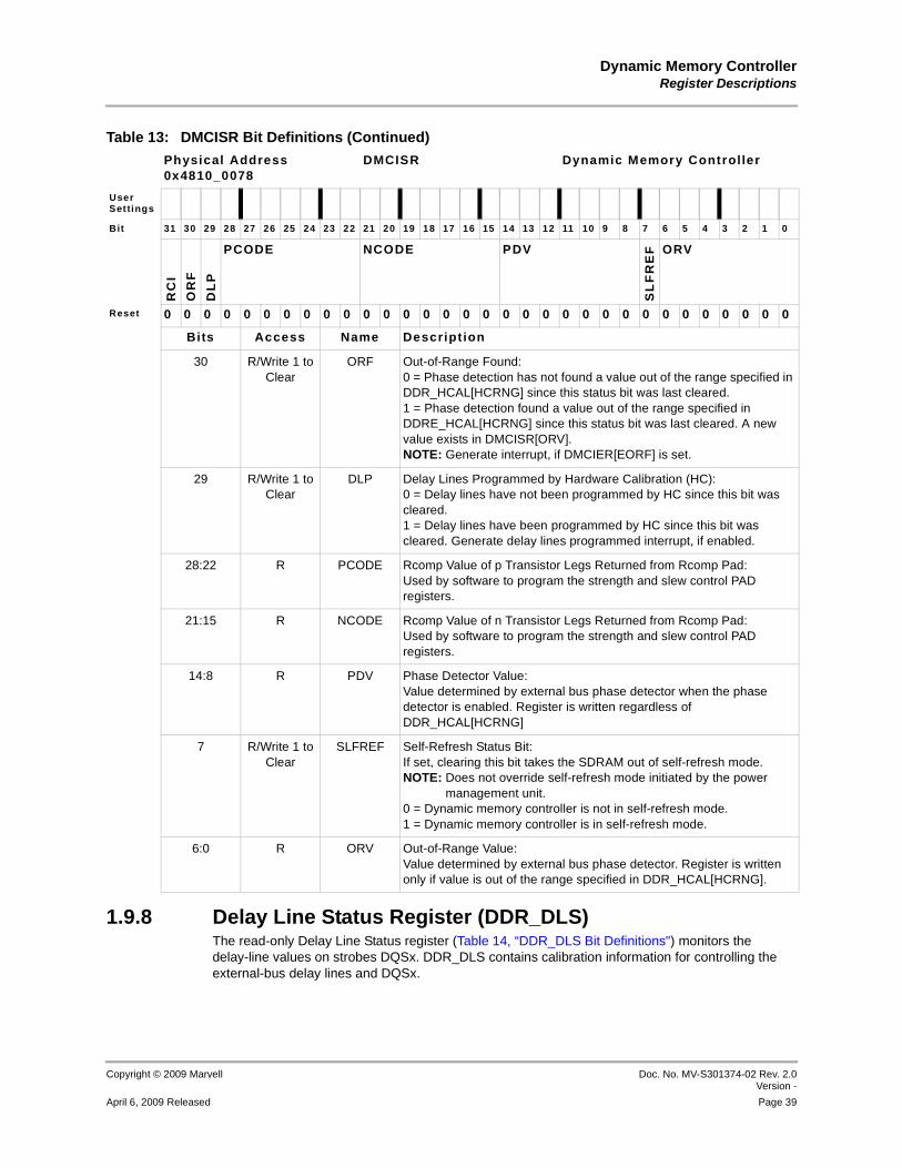
Dynamic Memory ControllerRegister Descriptions
Copyright © 2009 Marvell Doc. No. MV-S301374-02 Rev. 2.0Version -
April 6, 2009 Released Page 39
12345678910111213141516171819202122232425262728293031323334353637383940414243444546474849505152535455565758
1.9.8 Delay Line Status Register (DDR_DLS)The read-only Delay Line Status register (Table 14, “DDR_DLS Bit Definitions") monitors the delay-line values on strobes DQSx. DDR_DLS contains calibration information for controlling the external-bus delay lines and DQSx.
30 R/Write 1 to Clear
ORF Out-of-Range Found:0 = Phase detection has not found a value out of the range specified in DDR_HCAL[HCRNG] since this status bit was last cleared.1 = Phase detection found a value out of the range specified in DDRE_HCAL[HCRNG] since this status bit was last cleared. A new value exists in DMCISR[ORV]. NOTE: Generate interrupt, if DMCIER[EORF] is set.
29 R/Write 1 to Clear
DLP Delay Lines Programmed by Hardware Calibration (HC):0 = Delay lines have not been programmed by HC since this bit was cleared.1 = Delay lines have been programmed by HC since this bit was cleared. Generate delay lines programmed interrupt, if enabled.
28:22 R PCODE Rcomp Value of p Transistor Legs Returned from Rcomp Pad:Used by software to program the strength and slew control PAD registers.
21:15 R NCODE Rcomp Value of n Transistor Legs Returned from Rcomp Pad:Used by software to program the strength and slew control PAD registers.
14:8 R PDV Phase Detector Value:Value determined by external bus phase detector when the phase detector is enabled. Register is written regardless of DDR_HCAL[HCRNG]
7 R/Write 1 to Clear
SLFREF Self-Refresh Status Bit:If set, clearing this bit takes the SDRAM out of self-refresh mode. NOTE: Does not override self-refresh mode initiated by the power
management unit.0 = Dynamic memory controller is not in self-refresh mode.1 = Dynamic memory controller is in self-refresh mode.
6:0 R ORV Out-of-Range Value:Value determined by external bus phase detector. Register is written only if value is out of the range specified in DDR_HCAL[HCRNG].
Table 13: DMCISR Bit Definitions (Continued)
Physical Address0x4810_0078
DMCISR Dynamic Memory Control ler
User Settings
Bit 31 30 29 28 27 26 25 24 23 22 21 20 19 18 17 16 15 14 13 12 11 10 9 8 7 6 5 4 3 2 1 0
RC
I
OR
F
DL
P
PCODE NCODE PDV
SL
FR
EF ORV
Reset 0 0 0 0 0 0 0 0 0 0 0 0 0 0 0 0 0 0 0 0 0 0 0 0 0 0 0 0 0 0 0 0
Bits Access Name Descript ion
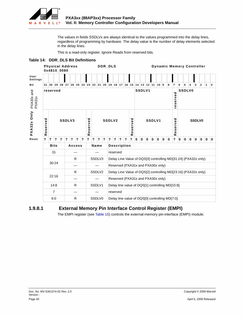
PXA3xx (88AP3xx) Processor Family Vol. II: Memory Controller Configuration Developers Manual
Doc. No. MV-S301374-02 Rev. 2.0 Version -
Copyright © 2009 Marvell
Page 40 April 6, 2009 Released
12345678910111213141516171819202122232425262728293031323334353637383940414243444546474849505152535455565758
The values in fields SSDLVx are always identical to the values programmed into the delay lines, regardless of programming by hardware. The delay value is the number of delay elements selected in the delay lines.
This is a read-only register. Ignore Reads from reserved bits.
1.9.8.1 External Memory Pin Interface Control Register (EMPI)The EMPI register (see Table 15) controls the external-memory pin-interface (EMPI) module.
Table 14: DDR_DLS Bit Definitions
Physical Address0x4810_0080
DDR_DLS Dynamic Memory Controller
User Settings
Bit 31 30 29 28 27 26 25 24 23 22 21 20 19 18 17 16 15 14 13 12 11 10 9 8 7 6 5 4 3 2 1 0
PX
A30
x an
d P
XA
31x
reserved SSDLV1
res
erv
ed
SSDLV0
PX
A3
2x
On
ly
Re
se
rve
d SSDLV3
Re
se
rve
d SSDLV2
Re
se
rve
d SSDLV1
Re
se
rve
d SSDLV0
Reset ? ? ? ? ? ? ? ? ? ? ? ? ? ? ? ? ? 0 0 0 0 0 0 0 ? 0 0 0 0 0 0 0
Bits Access Name Descript ion
31 — — reserved
30:24R SSDLV3 Delay Line Value of DQS[3] controlling MD[31:24] (PXA32x only)
— — Reserved (PXA31x and PXA30x only)
22:16R SSDLV2 Delay Line Value of DQS[2] controlling MD[23:16] (PXA32x only)
— — Reserved (PXA31x and PXA30x only)
14:8 R SSDLV1 Delay line value of DQS[1] controlling MD[15:8].
7 — — reserved
6:0 R SSDLV0 Delay line value of DQS[0] controlling MD[7:0].
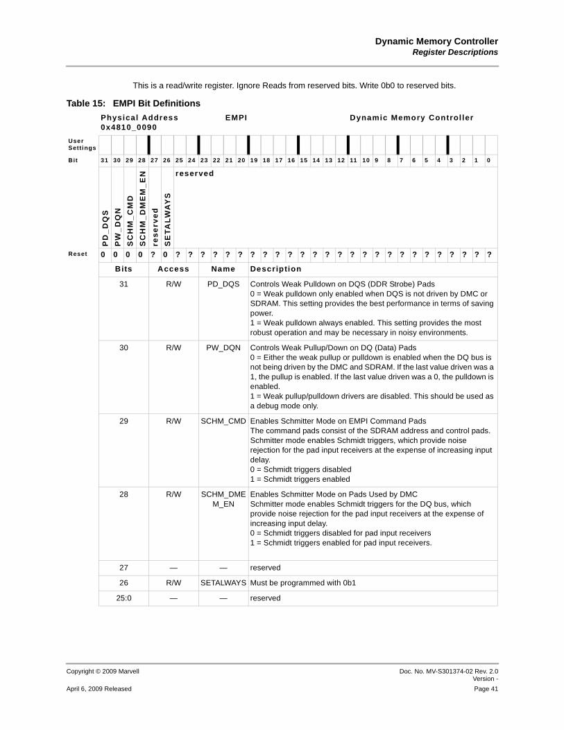
Dynamic Memory ControllerRegister Descriptions
Copyright © 2009 Marvell Doc. No. MV-S301374-02 Rev. 2.0Version -
April 6, 2009 Released Page 41
12345678910111213141516171819202122232425262728293031323334353637383940414243444546474849505152535455565758
This is a read/write register. Ignore Reads from reserved bits. Write 0b0 to reserved bits.
Table 15: EMPI Bit Definitions
Physical Address0x4810_0090
EMPI Dynamic Memory Control ler
User Settings
Bit 31 30 29 28 27 26 25 24 23 22 21 20 19 18 17 16 15 14 13 12 11 10 9 8 7 6 5 4 3 2 1 0
PD
_D
QS
PW
_D
QN
SC
HM
_C
MD
SC
HM
_D
ME
M_
EN
res
erv
ed
SE
TA
LW
AY
Sreserved
Reset 0 0 0 0 ? 0 ? ? ? ? ? ? ? ? ? ? ? ? ? ? ? ? ? ? ? ? ? ? ? ? ? ?
Bits Access Name Description
31 R/W PD_DQS Controls Weak Pulldown on DQS (DDR Strobe) Pads0 = Weak pulldown only enabled when DQS is not driven by DMC or SDRAM. This setting provides the best performance in terms of saving power.1 = Weak pulldown always enabled. This setting provides the most robust operation and may be necessary in noisy environments.
30 R/W PW_DQN Controls Weak Pullup/Down on DQ (Data) Pads0 = Either the weak pullup or pulldown is enabled when the DQ bus is not being driven by the DMC and SDRAM. If the last value driven was a 1, the pullup is enabled. If the last value driven was a 0, the pulldown is enabled. 1 = Weak pullup/pulldown drivers are disabled. This should be used as a debug mode only.
29 R/W SCHM_CMD Enables Schmitter Mode on EMPI Command PadsThe command pads consist of the SDRAM address and control pads. Schmitter mode enables Schmidt triggers, which provide noise rejection for the pad input receivers at the expense of increasing input delay.0 = Schmidt triggers disabled1 = Schmidt triggers enabled
28 R/W SCHM_DMEM_EN
Enables Schmitter Mode on Pads Used by DMCSchmitter mode enables Schmidt triggers for the DQ bus, which provide noise rejection for the pad input receivers at the expense of increasing input delay. 0 = Schmidt triggers disabled for pad input receivers1 = Schmidt triggers enabled for pad input receivers.
27 — — reserved
26 R/W SETALWAYS Must be programmed with 0b1
25:0 — — reserved

PXA3xx (88AP3xx) Processor Family Vol. II: Memory Controller Configuration Developers Manual
Doc. No. MV-S301374-02 Rev. 2.0 Version -
Copyright © 2009 Marvell
Page 42 April 6, 2009 Released
12345678910111213141516171819202122232425262728293031323334353637383940414243444546474849505152535455565758
1.9.8.2 Rcomp Control Register (RCOMP)The Rcomp Control register (Table 16, “RCOMP Bit Definitions") is similar in concept to the SDRAM Refresh Control register, MDREFR. Both registers use a counter clocked off of a 13-MHz clock to initiate events, and both registers contain an identical software mechanism for initiating their respective events.
This is a read/write register. Ignore Reads from reserved bits. Write 0b0 to reserved bits.
Table 16: RCOMP Bit Definitions
Physical Address0x4810_0100 RCOMP Dynamic Memory Controller
User Settings
Bit 31 30 29 28 27 26 25 24 23 22 21 20 19 18 17 16 15 14 13 12 11 10 9 8 7 6 5 4 3 2 1 0
SW
EVA
L
UP
DA
TE
RCRNG
SE
TALW
AY
S
reserved REI
Reset 0 0 0 0 0 0 0 0 ? ? ? ? 0 0 0 0 0 0 0 0 0 0 0 0 0 0 0 0 0 0 0 0
Bits Access Name Descript ion
31 R/W SWEVAL Software Rcomp Evaluation Request1 = Initiates an RCOMP evaluation cycle. 0 = Has no effect. NOTE: This bit is automatically cleared by hardware when the cycle is
complete.NOTE: Setting SWEVAL performs the same operation that occurs when
the REI counter expires.
30 R/W UPDATE UpdateSoftware must set this bit once the Programmable Buffer Strength and Slew Registers have been updated. 1 = The DMC initiates a EMPI NOP cycle and programs the EMPI pads with the values programmed in the Programmable Buffer Strength and Slew Registers. 0 = Has no effect. NOTE: This bit is automatically cleared by hardware when the cycle is
complete.
29:25 R/W RCRNG Resistive Compensation RangeIf RCOMP interrupt is enabled, the processor is interrupted if the new RCOMP value falls out of the range specified in this field. New RCOMP PCODE ≥ DMCISR[PCODE] + RCRNGNew RCOMP PCODE ≤ DMCISR[PCODE] - RCRNGNew RCOMP NCODE ≥ DMCISR[NCODE] + RCRNGNew RCOMP NCODE ≤ DMCISR[NCODE] - RCRNGNOTE: The processor is interrupted if the new values are out of range
and the DMCIER[ERCI] bit is set.NOTE: If RCRNG is set to 0, the processor is interrupted every time the
REI counter expires.
24 R/W SETALWAYS Must be programmed with 0b1
23:20 — — reserved
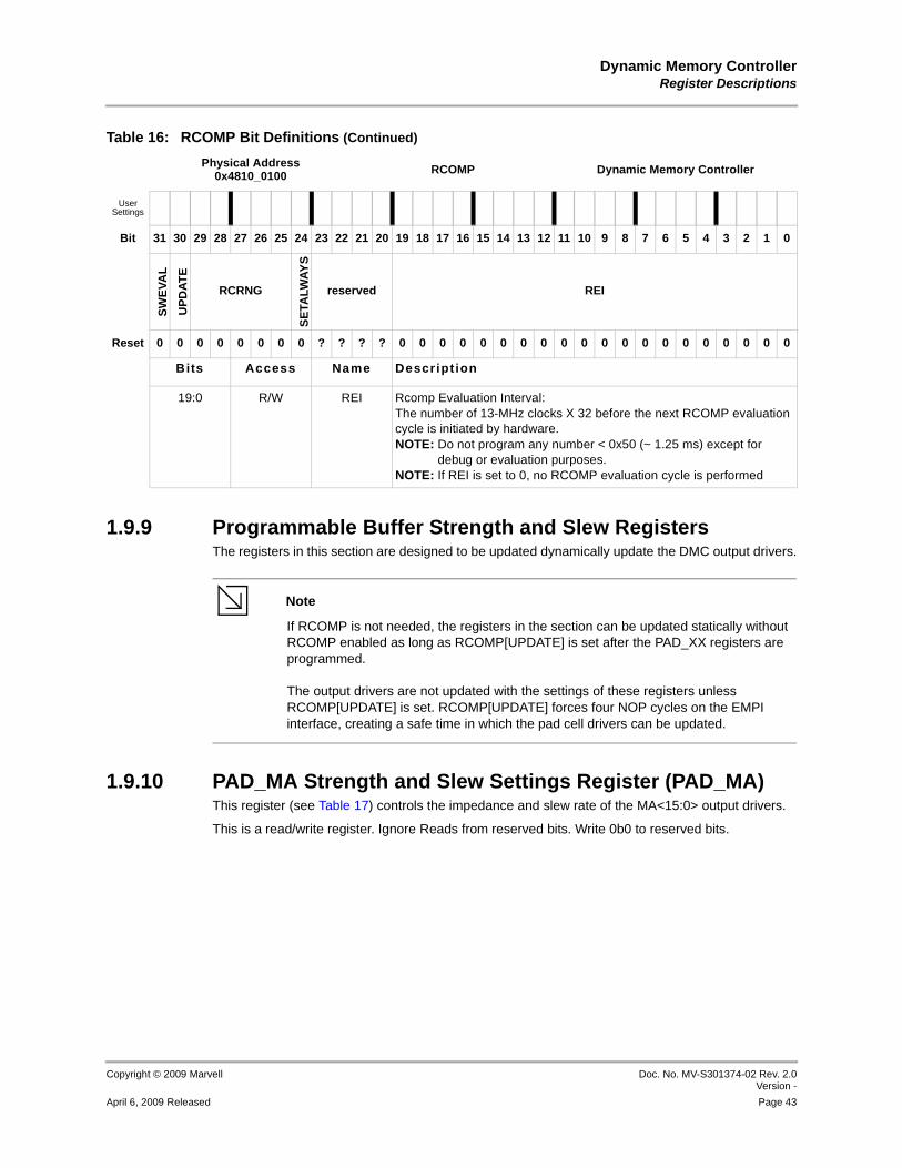
Dynamic Memory ControllerRegister Descriptions
Copyright © 2009 Marvell Doc. No. MV-S301374-02 Rev. 2.0Version -
April 6, 2009 Released Page 43
12345678910111213141516171819202122232425262728293031323334353637383940414243444546474849505152535455565758
1.9.9 Programmable Buffer Strength and Slew RegistersThe registers in this section are designed to be updated dynamically update the DMC output drivers.
Note
Note If RCOMP is not needed, the registers in the section can be updated statically without RCOMP enabled as long as RCOMP[UPDATE] is set after the PAD_XX registers are programmed.
The output drivers are not updated with the settings of these registers unless RCOMP[UPDATE] is set. RCOMP[UPDATE] forces four NOP cycles on the EMPI interface, creating a safe time in which the pad cell drivers can be updated.
1.9.10 PAD_MA Strength and Slew Settings Register (PAD_MA)This register (see Table 17) controls the impedance and slew rate of the MA<15:0> output drivers.
This is a read/write register. Ignore Reads from reserved bits. Write 0b0 to reserved bits.
19:0 R/W REI Rcomp Evaluation Interval:The number of 13-MHz clocks X 32 before the next RCOMP evaluation cycle is initiated by hardware. NOTE: Do not program any number < 0x50 (~ 1.25 ms) except for
debug or evaluation purposes.NOTE: If REI is set to 0, no RCOMP evaluation cycle is performed
Table 16: RCOMP Bit Definitions (Continued)
Physical Address0x4810_0100 RCOMP Dynamic Memory Controller
User Settings
Bit 31 30 29 28 27 26 25 24 23 22 21 20 19 18 17 16 15 14 13 12 11 10 9 8 7 6 5 4 3 2 1 0
SW
EVA
L
UP
DA
TE
RCRNGS
ETA
LWA
YS
reserved REI
Reset 0 0 0 0 0 0 0 0 ? ? ? ? 0 0 0 0 0 0 0 0 0 0 0 0 0 0 0 0 0 0 0 0
Bits Access Name Descript ion
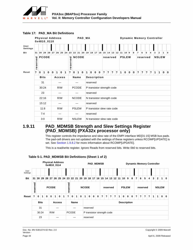
PXA3xx (88AP3xx) Processor Family Vol. II: Memory Controller Configuration Developers Manual
Doc. No. MV-S301374-02 Rev. 2.0 Version -
Copyright © 2009 Marvell
Page 44 April 6, 2009 Released
12345678910111213141516171819202122232425262728293031323334353637383940414243444546474849505152535455565758
1.9.11 PAD_MDMSB Strength and Slew Settings Register (PAD_MDMSB) (PXA32x processor only)This register controls the impedance and slew rate of the EMPI interface MD[31:15] MSB bus pads. The pad-cell drivers are not updated with the settings of these registers unless RCOMP[UPDATE] is set. See Section 1.9.8.2 for more information about RCOMP[UPDATE].
This is a read/write register. Ignore Reads from reserved bits. Write 0b0 to reserved bits.
Table 17: PAD_MA Bit Definitions
Physical Address0x4810_0110
PAD_MA Dynamic Memory Controller
User Settings
Bit 31 30 29 28 27 26 25 24 23 22 21 20 19 18 17 16 15 14 13 12 11 10 9 8 7 6 5 4 3 2 1 0
res
erv
ed PCODE
res
erv
ed NCODE reserved PSLEW reserved NSLEW
Reset ? 0 1 0 0 1 0 1 ? 0 1 0 1 0 0 0 ? ? ? ? 1 0 0 0 ? ? ? ? 1 1 0 0
Bits Access Name Descript ion
31 — — reserved
30:24 R/W PCODE P transistor strength code
23 — — reserved
22:16 R/W NCODE N transistor strength code
15:12 — — reserved
11:8 R/W PSLEW P transistor slew rate code
7:4 — — reserved
3:0 R/W NSLEW N transistor slew rate code
Table 5-1. PAD_MDMSB Bit Definitions (Sheet 1 of 2)
Physical Address0x4810_0114 PAD_MDMSB Dynamic Memory Controller
User Settings
Bit 31 30 29 28 27 26 25 24 23 22 21 20 19 18 17 16 15 14 13 12 11 10 9 8 7 6 5 4 3 2 1 0
rese
rved
PCODE
rese
rved
NCODE reserved PSLEW reserved NSLEW
Reset ? 0 1 0 0 1 0 1 ? 0 1 0 1 0 0 0 ? ? ? ? 1 0 0 0 ? ? ? ? 1 1 0 0
Bits Access Name Description
31 — — reserved
30:24 R/W PCODE P transistor strength code
23 — — reserved

Dynamic Memory ControllerRegister Descriptions
Copyright © 2009 Marvell Doc. No. MV-S301374-02 Rev. 2.0Version -
April 6, 2009 Released Page 45
12345678910111213141516171819202122232425262728293031323334353637383940414243444546474849505152535455565758
1.9.12 PAD_MDLSB Strength and Slew Settings Register (PAD_MDLSB)This register (Table 18, “PAD_MDLSB Bit Definitions") controls the impedance and slew rate of the MD<15:0>, DQM<3:0>, and DQS<3:0> output drivers.
This is a read/write register. Ignore Reads from reserved bits. Write 0b0 to reserved bits.
22:16 R/W NCODE N transistor strength code
15:12 — — reserved
11:8 R/W PSLEW P transistor slew rate code
7:4 — — reserved
3:0 R/W NSLEW N transistor slew rate code
Table 5-1. PAD_MDMSB Bit Definitions (Sheet 2 of 2)
Physical Address0x4810_0114 PAD_MDMSB Dynamic Memory Controller
User Settings
Bit 31 30 29 28 27 26 25 24 23 22 21 20 19 18 17 16 15 14 13 12 11 10 9 8 7 6 5 4 3 2 1 0
rese
rved
PCODE
rese
rved
NCODE reserved PSLEW reserved NSLEW
Reset ? 0 1 0 0 1 0 1 ? 0 1 0 1 0 0 0 ? ? ? ? 1 0 0 0 ? ? ? ? 1 1 0 0
Bits Access Name Description
Table 18: PAD_MDLSB Bit Definitions
Physical Address0x4810_0118
PAD_MDLSB Dynamic Memory Control ler
User Settings
Bit 31 30 29 28 27 26 25 24 23 22 21 20 19 18 17 16 15 14 13 12 11 10 9 8 7 6 5 4 3 2 1 0
res
erv
ed PCODE
res
erv
ed NCODE reserved PSLEW reserved NSLEW
Reset ? 0 1 0 0 1 0 1 ? 0 1 0 1 0 0 0 ? ? ? ? 1 0 0 0 ? ? ? ? 1 1 0 0
Bits Access Name Descript ion
31 — — reserved
30:24 R/W PCODE P transistor strength code
23 — — reserved
22:16 R/W NCODE N transistor strength code
15:12 — — reserved
11:8 R/W PSLEW P transistor slew rate code
7:4 — — reserved
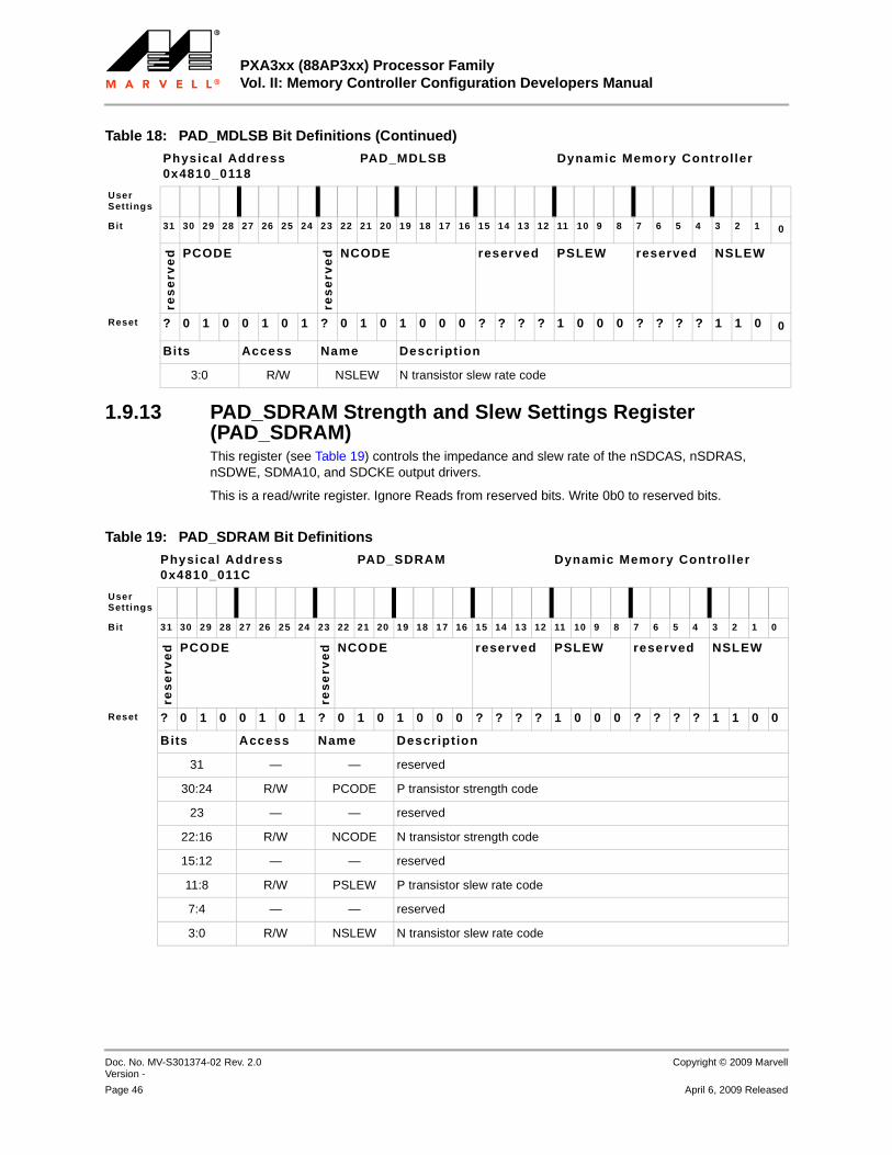
PXA3xx (88AP3xx) Processor Family Vol. II: Memory Controller Configuration Developers Manual
Doc. No. MV-S301374-02 Rev. 2.0 Version -
Copyright © 2009 Marvell
Page 46 April 6, 2009 Released
12345678910111213141516171819202122232425262728293031323334353637383940414243444546474849505152535455565758
1.9.13 PAD_SDRAM Strength and Slew Settings Register (PAD_SDRAM)This register (see Table 19) controls the impedance and slew rate of the nSDCAS, nSDRAS, nSDWE, SDMA10, and SDCKE output drivers.
This is a read/write register. Ignore Reads from reserved bits. Write 0b0 to reserved bits.
3:0 R/W NSLEW N transistor slew rate code
Table 18: PAD_MDLSB Bit Definitions (Continued)
Physical Address0x4810_0118
PAD_MDLSB Dynamic Memory Control ler
User Settings
Bit 31 30 29 28 27 26 25 24 23 22 21 20 19 18 17 16 15 14 13 12 11 10 9 8 7 6 5 4 3 2 1 0
res
erv
ed PCODE
res
erv
ed NCODE reserved PSLEW reserved NSLEW
Reset ? 0 1 0 0 1 0 1 ? 0 1 0 1 0 0 0 ? ? ? ? 1 0 0 0 ? ? ? ? 1 1 0 0
Bits Access Name Descript ion
Table 19: PAD_SDRAM Bit Definitions
Physical Address0x4810_011C
PAD_SDRAM Dynamic Memory Controller
User Settings
Bit 31 30 29 28 27 26 25 24 23 22 21 20 19 18 17 16 15 14 13 12 11 10 9 8 7 6 5 4 3 2 1 0
res
erv
ed PCODE
res
erv
ed NCODE reserved PSLEW reserved NSLEW
Reset ? 0 1 0 0 1 0 1 ? 0 1 0 1 0 0 0 ? ? ? ? 1 0 0 0 ? ? ? ? 1 1 0 0
Bits Access Name Descript ion
31 — — reserved
30:24 R/W PCODE P transistor strength code
23 — — reserved
22:16 R/W NCODE N transistor strength code
15:12 — — reserved
11:8 R/W PSLEW P transistor slew rate code
7:4 — — reserved
3:0 R/W NSLEW N transistor slew rate code
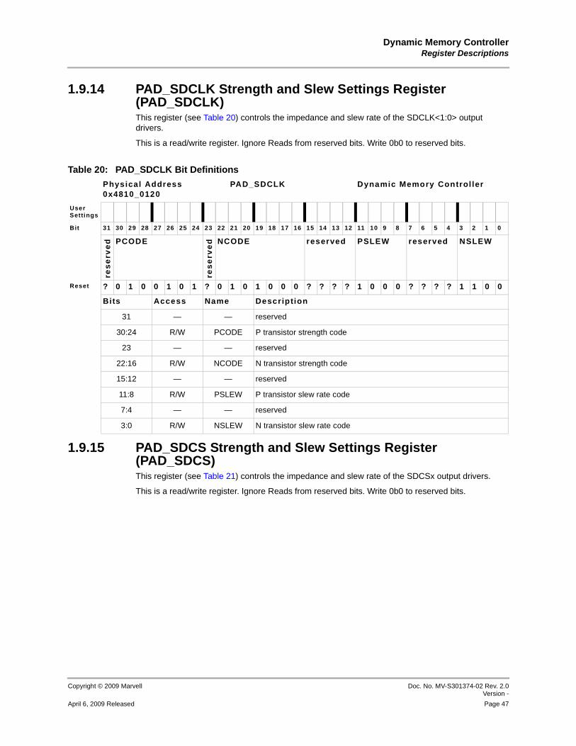
Dynamic Memory ControllerRegister Descriptions
Copyright © 2009 Marvell Doc. No. MV-S301374-02 Rev. 2.0Version -
April 6, 2009 Released Page 47
12345678910111213141516171819202122232425262728293031323334353637383940414243444546474849505152535455565758
1.9.14 PAD_SDCLK Strength and Slew Settings Register (PAD_SDCLK)This register (see Table 20) controls the impedance and slew rate of the SDCLK<1:0> output drivers.
This is a read/write register. Ignore Reads from reserved bits. Write 0b0 to reserved bits.
1.9.15 PAD_SDCS Strength and Slew Settings Register (PAD_SDCS)This register (see Table 21) controls the impedance and slew rate of the SDCSx output drivers.
This is a read/write register. Ignore Reads from reserved bits. Write 0b0 to reserved bits.
Table 20: PAD_SDCLK Bit Definitions
Physical Address0x4810_0120
PAD_SDCLK Dynamic Memory Control ler
User Settings
Bit 31 30 29 28 27 26 25 24 23 22 21 20 19 18 17 16 15 14 13 12 11 10 9 8 7 6 5 4 3 2 1 0
res
erv
ed PCODE
res
erv
ed NCODE reserved PSLEW reserved NSLEW
Reset ? 0 1 0 0 1 0 1 ? 0 1 0 1 0 0 0 ? ? ? ? 1 0 0 0 ? ? ? ? 1 1 0 0
Bits Access Name Description
31 — — reserved
30:24 R/W PCODE P transistor strength code
23 — — reserved
22:16 R/W NCODE N transistor strength code
15:12 — — reserved
11:8 R/W PSLEW P transistor slew rate code
7:4 — — reserved
3:0 R/W NSLEW N transistor slew rate code

PXA3xx (88AP3xx) Processor Family Vol. II: Memory Controller Configuration Developers Manual
Doc. No. MV-S301374-02 Rev. 2.0 Version -
Copyright © 2009 Marvell
Page 48 April 6, 2009 Released
12345678910111213141516171819202122232425262728293031323334353637383940414243444546474849505152535455565758
Table 21: PAD_SDCS Bit Definitions
Physical Address0x4810_0124
PAD_SDCS Dynamic Memory Control ler
User Settings
Bit 31 30 29 28 27 26 25 24 23 22 21 20 19 18 17 16 15 14 13 12 11 10 9 8 7 6 5 4 3 2 1 0
res
erv
ed PCODE
res
erv
ed NCODE reserved PSLEW reserved NSLEW
Reset ? 0 1 0 0 1 0 1 ? 0 1 0 1 0 0 0 ? ? ? ? 1 0 0 0 ? ? ? ? 1 1 0 0
Bits Access Name Description
31 — — reserved
30:24 R/W PCODE P transistor strength code
23 — — reserved
22:16 R/W NCODE N transistor strength code
15:12 — — reserved
11:8 R/W PSLEW P transistor slew rate code
7:4 — — reserved
3:0 R/W NSLEW N transistor slew rate code
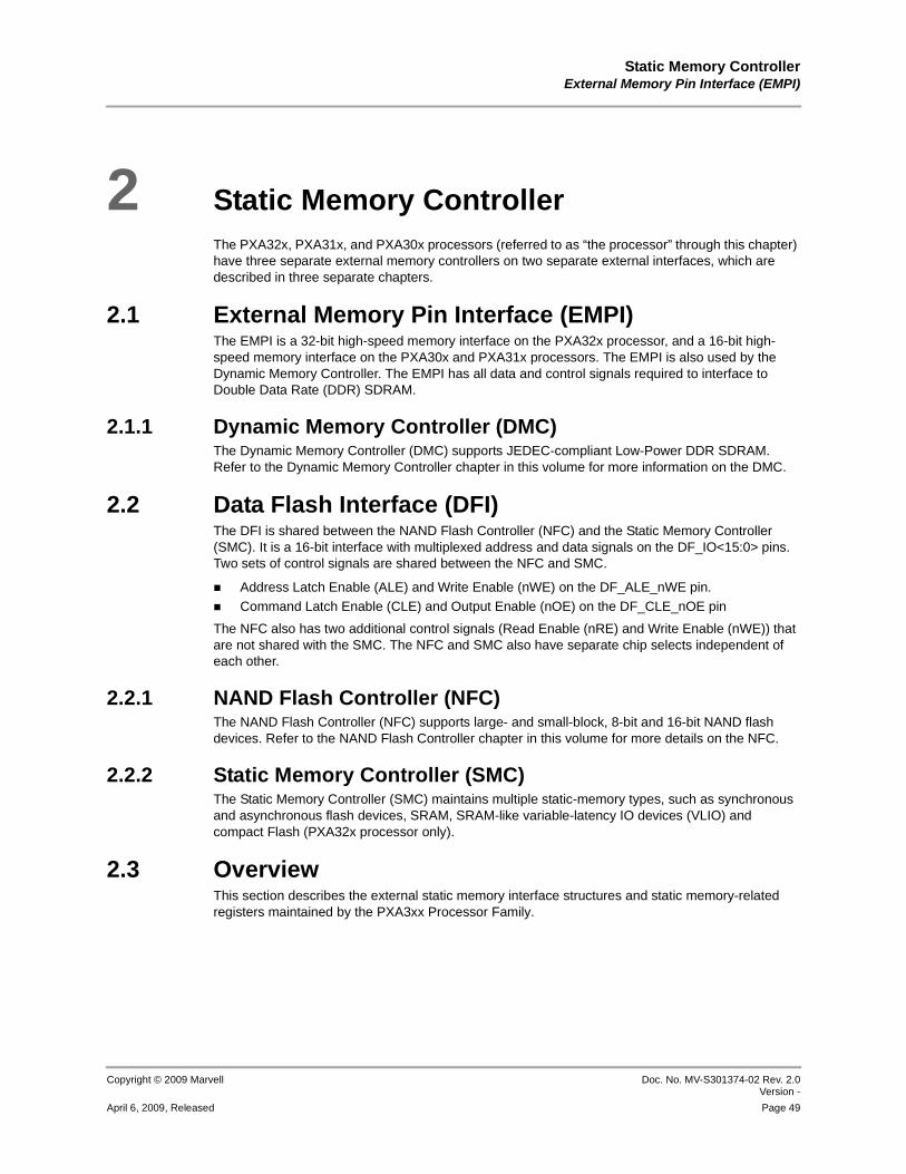
Static Memory ControllerExternal Memory Pin Interface (EMPI)
Copyright © 2009 Marvell Doc. No. MV-S301374-02 Rev. 2.0Version -
April 6, 2009, Released Page 49
2 Static Memory ControllerThe PXA32x, PXA31x, and PXA30x processors (referred to as “the processor” through this chapter) have three separate external memory controllers on two separate external interfaces, which are described in three separate chapters.
2.1 External Memory Pin Interface (EMPI)The EMPI is a 32-bit high-speed memory interface on the PXA32x processor, and a 16-bit high- speed memory interface on the PXA30x and PXA31x processors. The EMPI is also used by the Dynamic Memory Controller. The EMPI has all data and control signals required to interface to Double Data Rate (DDR) SDRAM.
2.1.1 Dynamic Memory Controller (DMC)The Dynamic Memory Controller (DMC) supports JEDEC-compliant Low-Power DDR SDRAM. Refer to the Dynamic Memory Controller chapter in this volume for more information on the DMC.
2.2 Data Flash Interface (DFI) The DFI is shared between the NAND Flash Controller (NFC) and the Static Memory Controller (SMC). It is a 16-bit interface with multiplexed address and data signals on the DF_IO<15:0> pins. Two sets of control signals are shared between the NFC and SMC.
Address Latch Enable (ALE) and Write Enable (nWE) on the DF_ALE_nWE pin.Command Latch Enable (CLE) and Output Enable (nOE) on the DF_CLE_nOE pin
The NFC also has two additional control signals (Read Enable (nRE) and Write Enable (nWE)) that are not shared with the SMC. The NFC and SMC also have separate chip selects independent of each other.
2.2.1 NAND Flash Controller (NFC)The NAND Flash Controller (NFC) supports large- and small-block, 8-bit and 16-bit NAND flash devices. Refer to the NAND Flash Controller chapter in this volume for more details on the NFC.
2.2.2 Static Memory Controller (SMC)The Static Memory Controller (SMC) maintains multiple static-memory types, such as synchronous and asynchronous flash devices, SRAM, SRAM-like variable-latency IO devices (VLIO) and compact Flash (PXA32x processor only).
2.3 OverviewThis section describes the external static memory interface structures and static memory-related registers maintained by the PXA3xx Processor Family.

PXA3xx (88AP3xx) Processor Family Vol. II: Memory Controller Configuration Developers Manual
Doc. No. MV-S301374-02 Rev. 2.0 Version -
Copyright © 2009 Marvell
Page 50 April 6, 2009, Released
2.3.1 PXA3xx Processor DifferencesTable 22 shows the Static Memory Controller differences among the PXA32x, PXA31x, and PXA30x processors.
2.4 FeaturesThe SMC provides the following features:
Interface to SRAM-like devices, variable latency I/O (VLIO) devices, and various types of execute-in-place (XIP) flash (including synchronous and asynchronous) and PC Card/Compact Flash (PXA32x processor only)Managed NAND devices (NAND devices with NOR flash/SRAM interface) including Samsung OneNAND* and SanDisk Mobile Disk on Chip* (mDOC).Each partition has a 28-bit logical address (with byte significance). For some of these devices, the space in the memory map may not be sufficient to use this range. For such situations, the address is padded with zeros. For more information on the SMC memory map, refer to Table 26, “Latched Address Signals” .
nCS0 and nCS1 support asynchronous flash, SRAM, VLIO, and synchronous flash (synchronous Reads and asynchronous Writes).nCS2 and nCS3 support asynchronous flash, SRAM, VLIO, synchronous flash (Reads and Writes) and synchronous (Reads and Writes) flash-type companion chips
2.4.1 AA/D MemoriesThe term “AA/D” refers to the way addresses and data are supplied to the external memory devices, and to the number of cycles on the DFI bus (DF_IO<15:0>) to produce an access. In AA/D multiplexed mode, no dedicated address pins are used; instead, two additional address cycles are provided before the data cycle. The upper address and tranceiver control signals are latched using nLUA (high-order addresses). The lower 16 address signals are latched using nLLA (low-order addresses).
2.4.2 Non-AA/D MemoriesThe SMC is optimized to operate with AA/D multiplexed memories, but non-multiplexed devices can be maintained using external address latches. The SMC can use two external latches to hold the address value that is sent out in two cycles on the data bus and latched with the nLUA and nLLA signals. This process maintains non-address/data multiplexed parts.
An optional “Latched Addressing Mode” is also maintained where the address lines are provided on separate GPIO pins. The same upper and lower address cycles are still sent out on the DFI bus, while the address signals are latched on the GPIO pins using the nLUA and nLLA signals.
Table 22: PXA3xx Processors Feature Differences
Feature PXA30x PXA31x PXA32x
Compact Flash Support Not Supported Not Supported Supported
Chip Selects 4 (nCS<3:0>) 4 (nCS<3:0>) 2 (nCS<3:2>)
Latched Addressing Mode
Supported Supported Not Supported
Extenal DMA Request signal
Not Supported Supported Supported

Static Memory ControllerSignal Descriptions
Copyright © 2009 Marvell Doc. No. MV-S301374-02 Rev. 2.0Version -
April 6, 2009, Released Page 51
2.5 Signal DescriptionsTable 23 describes the input and output signals from the SMC. Only signals used by the SMC are listed. DMC and NFC signals can be found in their respective chapters.
Table 23: Static Memory Controller External Signal Descriptions
Ball Name Signal Name
Direct ion Descript ion
Arbitrated DFI Signals
DF_IO<15:0> DF_IO<15:0> Input/Output Bidirectional DFI data/address bus
DF_ALE_NWE DF_nWE Output Write enable (PXA30x and PXA31x processors only)
DF_ALE_NWE1 and DF_ALE_NWE2
DF_nWE Output Write enable (PXA32x processor only)
DF_ALE_NOE DF_nOE Output Output enable
Non-Arbitrated DFI Signals
DF_SCLK_E DF_SCLK Output Output clock for synchronous accessesNOTE: The Application Subsystem Clock Control Unit provides
the clock for the SMC through the Application Subsystem Clock Control Register (ACCR[SMCFS]). This clock is then divided using the MEMCLKCFG[DF_CLKDIV] register to output the correct frequency.
GPIO4GPIO3
nCS3nCS2
Output Chip selects (PXA32x processor only)
GPIO2GPIO1nCS1nCS0
nCS3nCS2nCS1nCS0
Output Chip selects (PXA30x and PXA31x processors only)
nLUA nLUA Output Latch upper address Used to latch the high-order address bits during the upper address cycle.
nLLA nLLA Output Latch lower address Used to latch the low-order address bits during the lower address cycle.
DF_ADDR<3:0> DF_ADDR<3:0>
Output Low-order address bits Used as the lowest four address bits during an asynchronous burst transfer of the values in the lower address cycle on the DF_IO<15:0> pins.
nBE<1:0> nBE<1:0> Output Data byte enable nBE<0> corresponds to DF_IO<7:0> nBE<1> corresponds to DF_IO<15:8> 0 = Do not mask out corresponding byte1 = Mask out corresponding byte

PXA3xx (88AP3xx) Processor Family Vol. II: Memory Controller Configuration Developers Manual
Doc. No. MV-S301374-02 Rev. 2.0 Version -
Copyright © 2009 Marvell
Page 52 April 6, 2009, Released
GPIO2 RDY Input Variable-Latency I/O Ready signal for inserting wait states. (PXA32x processor only)0 = Wait1 = VLIO is ready
GPIO0 RDY Input Variable-Latency I/O Ready signal for inserting wait states. (PXA30x and PXA31x processors Only)0 = Wait1 = VLIO is ready
nXCVREN nXCVREN Output External transceiver enable (PXA32x processor Only)This signal can be used to enable an external transceiver. It is asserted along with the Output Enable (nOE) pin during read accesses and one DF_SLCK cycle before the Write Enable (nWE) pin during write accesses.0 = Enable transceiver 1 = Disable transceiver
GPIO2 nXCVREN Output External transceiver enable (PXA30x and PXA31x processors Only)This signal can be used to enable an external transceiver. It is asserted along with the Output Enable (nOE) pin during read accesses and one DF_SLCK cycle before the Write Enable (nWE) pin during write accesses.0 = Enable transceiver 1 = Disable transceiver
A31 (DF_IO<15>) during the nLUA address cycle
RDnWR Output Used to determine which direction the transceiver operates.0 = Indicates a write. The transceiver drives towards the external
devices.1 = Indicates a read. The transceiver drives toward the PXA3xx
Processor Family.
GPIO0 DREQ Input Static Memory Controller DMA request line (PXA32x processor only)The external SMC chip asserts the DREQ signal when a DMA transfer is required. The DREQ signal must remain asserted for four DF_SCLK cycles to allow the DMA Controller to recognize a low-to-high transition.
GPIO0 DREQ1 Input Static Memory Controller DMA request line (PXA31x processor only)The external SMC chip asserts the DREQ signal when a DMA transfer is required. The DREQ signal must remain asserted for four DF_SCLK cycles to allow the DMA Controller to recognize a low-to-high transition.
GPIO1 DREQ2 Input Static Memory Controller DMA request line (PXA31x processor only)The external SMC chip asserts the DREQ signal when a DMA transfer is required. The DREQ signal must remain asserted for four DF_SCLK cycles to allow the DMA Controller to recognize a low-to-high transition.
Table 23: Static Memory Controller External Signal Descriptions (Continued)
Ball Name Signal Name
Direct ion Descript ion
Static Memory ControllerOperation
Copyright © 2009 Marvell Doc. No. MV-S301374-02 Rev. 2.0Version -
April 6, 2009, Released Page 53
2.6 OperationThe SMC is used to connect to external memory devices through the DFI bus. This section details the architecture of the SMC and how it is configured for different memory types.
2.6.1 Transfer Processing OrderMemory requests are placed in a four-deep processing queue for each initiator source, for example, the core or the system buses, and processed in the order they are received from each source. No out-of-order processing is performed. Multiple requests are always processed in the order received independent of which initiator sent the request. For more information, refer to the Memory Switch chapter in Volume I.
2.6.1.1 Frequency ChangeFollow these requirements when changing the SMC fequency and DF_SCLK frequency:
GPIO2 DREQ3 Input Static Memory Controller DMA request line (PXA31x processor only)The external SMC chip asserts the DREQ signal when a DMA transfer is required. The DREQ signal must remain asserted for four DF_SCLK cycles to allow the DMA Controller to recognize a low-to-high transition.
PC Card Control Signals (Non-Arbitrated DFI) (PXA32x processor only)
GPIO5 nPIOR Output Card interface I/O space output enable
GPIO6 nPIOW Output Card interface I/O space write enable
GPIO7 nIOIS16 Input Card interface input from I/O space telling size of data bus.0 = 16-bit I/O space1 = 8-bit I/O space
GPIO8 nPWAIT Input Card interface input for inserting wait states.0 = Wait1 = Card is ready
A30, nLUAA29,nLUA
nPCE<2:1> Output Byte Lane enable for the card interfacenPCE1 - DF_IO<7:0> enablenPCE2 - DF_IO<15:8> enableThese signals are not provided as separate pins. Instead they are multiplexed onto the data bus and held in external latches like the address signals. See Section 2.7. nPCE1 signal is latched during nLUA assertion as A29 (DF_IO[13]). nPCE2 signal is latched during nLUA assertion as A30 (DF_IO[14]).
A26, nLUA nPREG Output Serves as the card interface address bit <26> and selects register space (I/O or attribute) versus memory spaceThis signal is not provided as a separate pin. Instead it is multiplexed onto the data bus and held in external latches like the address signals. See Section 2.7. This signal is latched during nLUA assertion as A26 (DF_IO[10]).
Table 23: Static Memory Controller External Signal Descriptions (Continued)
Ball Name Signal Name
Direct ion Descript ion
PXA3xx (88AP3xx) Processor Family Vol. II: Memory Controller Configuration Developers Manual
Doc. No. MV-S301374-02 Rev. 2.0 Version -
Copyright © 2009 Marvell
Page 54 April 6, 2009, Released
When decreasing frequencies from 208 MHz (ACCR[SMCFS] = 0b101) to 104 MHz (ACCR[SMCFS] = 0b010), the SMC frequency (ACCR[SMCFS]) must be lowered first, followed by the clock divisor (MEMCLKCFG[DF_CLKDIV]).
When increasing frequencies from 104 MHz (ACCR[SMCFS] = 0b010) to 208 MHz (ACCR[SMCFS] = 0b101), the clock divisor (MEMCLKCFG[DF_CLKDIV]) must be changed first, followed by the SMC frequency (ACCR[SMCFS]). When changing the DF_SCLK to a different frequency (52 MHz to 19.5 MHz), the SXCNCFG, MSCx, and SXCNFG registers must be changed to match the external device timing requirements.This change in frequencies must occur while the SMC is idle and no accesses are occuring.
Note
Note For more information on frequency changes and the Application Subsystem Clock Configuration Register (ACCR), refer to Chapter 6 “Clock Controllers and Power Management” in PXA3xx Processor Family Vol. I: System and Timer Configuration Developers Manual
2.6.2 ResetAt reset de-assertion, all SMC registers default to their reset values. They must be configured appropriately, depending on which devices the memory controller is interfacing to, before any accesses can be performed. Refer to Section 2.6.8 for the proper sequence of programming the SMC registers.
Note
Note Refer to the PXA3xx Processor Boot ROM Reference Manual for more information on the requirements for booting from an SMC chip select.
2.6.3 Memory MapThe SMC has four separate partitions that are shown in Table 24. For more infomation on the PXA3xx Processor Family memory map, refer to the Memory Map chapter in PXA3xx Processor Family Vol. I: System and Timer Configuration Developers Manual.
Table 24: Static Memory Controller Address Map
Name Address Region
nCS0 0x0000_0000–0x0FFF_FFFF (256 Mbyte) (PXA30x and PXA31x processors only)
nCS1 0x3000_0000–0x3FFF_FFFF (256 Mbyte) (PXA30x and PXA31x processors only)
nCS2 0x1000_0000–0x13FF_FFFF (64 Mbyte)
nCS3 0x1400_0000–0x17FF_FFFF (64 Mbyte)
Card Memory 0x2000_0000–0x2FFF_FFFF (256 Mbyte) (PXA32x processor only)
Static Memory ControllerOperation
Copyright © 2009 Marvell Doc. No. MV-S301374-02 Rev. 2.0Version -
April 6, 2009, Released Page 55
2.6.4 Memory Interface OptionsThe memory type on a particular chip select is configured by the CSADRCFGx, MSCx and SXCNFGx registers for that chip select.
2.6.4.1 Restrictions on Chip-Select UseEach chip select can be configured for any of the legal memory types defined by CSADRCFG[INFTYPE]. No checking is performed to ensure that a particular memory type is allowable on the chip select for which it is configured. When using two flash devices on separate chip selects, both chip selects must be configured identically with the same size and frequency.
Note
Note The restriction on flash devices does not stop nCS2 being flash and nCS3 being a non-flash device. It merely states that if both are flash, then they must be identical.
2.6.4.2 DFI Transceiver ControlExternal transceivers can be used for each address latch phase (nLUA/nLLA) on latches positioned between the PXA3xx Processor Family and external devices controlled. The transceivers are controlled using the nXCVREN and RDnWR signals. When using multiple SMC devices, the transceiver should be enabled only when the connected device is being accessed.
2.6.5 Types and Sizes of Memory AccessesThe SMC can generate only certain types of memory access. No accesses can cross an aligned 32-byte boundary. On a 16-bit data bus, each full-word access becomes two half-word accesses, with address bit 1 always starting at 0.
2.6.6 Byte Enables and Byte AddressThe PXA3xx Processor Family calculates 28 bits of byte address for accesses of up to 256 MB per chip select (nCS0 and nCS1). For nCS2 and nCS3 chip select address accesses up to 64 MB, the upper bits are not used and are held zero. This byte address is then formatted to be sent out in two parts, according to the programming of the Address Configuration Registers (CSADRCFGx).
Table 25 shows the least significant bit of the logical address. This address may not actually come out of the chip, depending on the setting of CSADRCFGx[ADDRBASE]. For example, if set to 0b01, then the least significant address sent out would be address <1>.
Where the byte address is of no concern, the lowest bit can be truncated (by not connecting the address at the system level or by using the CSADRCFGx controls). For all Reads, the byte address bits are 0. For Writes, the byte address bits are summarized in Table 25.
Note
Note The SMC maintains byte addressing but not byte interfaces.
PXA3xx (88AP3xx) Processor Family Vol. II: Memory Controller Configuration Developers Manual
Doc. No. MV-S301374-02 Rev. 2.0 Version -
Copyright © 2009 Marvell
Page 56 April 6, 2009, Released
2.6.6.1 Aborts and Nonexistent MemoryAccesses to or from unpopulated memory locations are not detected in hardware. When no memory is selected on a Read, indeterminate data is returned.
Reads and Writes to or from the unoccupied portion are processed as if the memory occupies the entire allocation of the memory partition if a memory is not occupying all allocated megabytes of a partition but is occupying only a portion. This memory processing is true for any memory type.
2.6.7 Addressing OperationsThe PXA3xx Processor Family provides a varying number of addressing bits. Various forms of address multiplexing enable connection to different types of memories. All address ranges are described based on the full byte address. Thus, the logical A<0> bit always has byte significance.
Here are general guidelines to follow for address configuration:
CSADRCFGx<ADDRBASE> should be 0b01, which means the lowest address bits (the byte address) are not required.CSADRCFG<ADDRSPLIT> should be 0b1001, which means physical internal address bit A<16:1> goes out on DF_IO<15:0> during the low address phase, and A<27:17> goes out on DF_IO<15:0> during the upper address phase.Each chip select can be configured to a different address configuration.No automatic configuration of address bits is performed. The Control register (CSADRCFGx) must be set up for the relevant chip select before an operation is performed. Inconsistent programming states behave incorrectly and are not permitted.
Table 25: 16-Bit Byte Address Bit Based on nBE<1:0>
nBE<1:0> Addr<0>
00 0
10 0
01 1
11 0
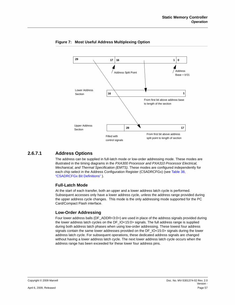
Static Memory ControllerOperation
Copyright © 2009 Marvell Doc. No. MV-S301374-02 Rev. 2.0Version -
April 6, 2009, Released Page 57
2.6.7.1 Address OptionsThe address can be supplied in full-latch mode or low-order addressing mode. These modes are illustrated in the timing diagrams in the PXA300 Processor and PXA310 Processor Electrical, Mechanical, and Thermal Specification (EMTS). These modes are configured independently for each chip select in the Address Configuration Register (CSADRCFGx) (see Table 38, “CSADRCFGx Bit Definitions” ).
Full-Latch ModeAt the start of each transfer, both an upper and a lower address latch cycle is performed. Subsequent accesses only have a lower address cycle, unless the address range provided during the upper address cycle changes. This mode is the only addressing mode supported for the PC Card/Compact Flash interface.
Low-Order AddressingFour lower address balls (DF_ADDR<3:0>) are used in place of the address signals provided during the lower address latch cycles on the DF_IO<15:0> signals. The full address range is supplied during both address latch phases when using low-order addressing. These lowest four address signals contain the same lower addresses provided on the DF_IO<15:0> signals during the lower address latch cycle. For subsequent operations, these dedicated address signals are changed without having a lower address latch cycle. The next lower address latch cycle occurs when the address range has been exceeded for these lower four address pins.
Figure 7: Most Useful Address Multiplexing Option
Address Split Point AddressBase = b’01
Lower AddressSection
Upper AddressSection
Filled with control signals
From first bit above address baseto length of the section
From first bit above addresssplit point to length of section
011617
17
1
29
29
16
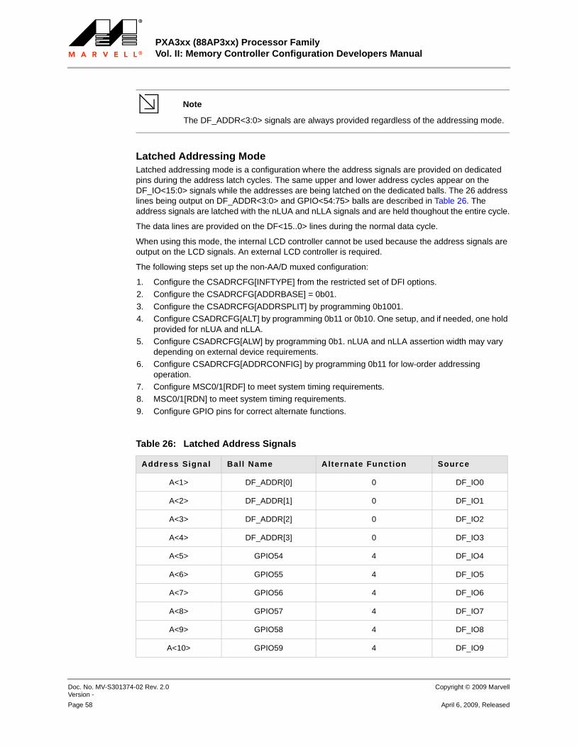
PXA3xx (88AP3xx) Processor Family Vol. II: Memory Controller Configuration Developers Manual
Doc. No. MV-S301374-02 Rev. 2.0 Version -
Copyright © 2009 Marvell
Page 58 April 6, 2009, Released
Note
Note The DF_ADDR<3:0> signals are always provided regardless of the addressing mode.
Latched Addressing ModeLatched addressing mode is a configuration where the address signals are provided on dedicated pins during the address latch cycles. The same upper and lower address cycles appear on the DF_IO<15:0> signals while the addresses are being latched on the dedicated balls. The 26 address lines being output on DF_ADDR<3:0> and GPIO<54:75> balls are described in Table 26. The address signals are latched with the nLUA and nLLA signals and are held thoughout the entire cycle.
The data lines are provided on the DF<15..0> lines during the normal data cycle.
When using this mode, the internal LCD controller cannot be used because the address signals are output on the LCD signals. An external LCD controller is required.
The following steps set up the non-AA/D muxed configuration:
1. Configure the CSADRCFG[INFTYPE] from the restricted set of DFI options.2. Configure the CSADRCFG[ADDRBASE] = 0b01.
3. Configure the CSADRCFG[ADDRSPLIT] by programming 0b1001.4. Configure CSADRCFG[ALT] by programming 0b11 or 0b10. One setup, and if needed, one hold
provided for nLUA and nLLA.5. Configure CSADRCFG[ALW] by programming 0b1. nLUA and nLLA assertion width may vary
depending on external device requirements.6. Configure CSADRCFG[ADDRCONFIG] by programming 0b11 for low-order addressing
operation.7. Configure MSC0/1[RDF] to meet system timing requirements.8. MSC0/1[RDN] to meet system timing requirements.
9. Configure GPIO pins for correct alternate functions.
Table 26: Latched Address Signals
Address Signal Ball Name Alternate Function Source
A<1> DF_ADDR[0] 0 DF_IO0
A<2> DF_ADDR[1] 0 DF_IO1
A<3> DF_ADDR[2] 0 DF_IO2
A<4> DF_ADDR[3] 0 DF_IO3
A<5> GPIO54 4 DF_IO4
A<6> GPIO55 4 DF_IO5
A<7> GPIO56 4 DF_IO6
A<8> GPIO57 4 DF_IO7
A<9> GPIO58 4 DF_IO8
A<10> GPIO59 4 DF_IO9

Static Memory ControllerOperation
Copyright © 2009 Marvell Doc. No. MV-S301374-02 Rev. 2.0Version -
April 6, 2009, Released Page 59
2.6.8 Programming Static Memory Control RegistersThis section is intended as an aid and not a substitute to the overall programming of the SMC. In particular, read the relevant register definitions carefully.
The programmable MSCx[RTx], CSADRCFG[INFTYPE] and SXCNFG[SXENx] fields combine together to specify the type of memory and timing.
2.6.8.1 SMC ConfigurationFollow these steps to configure the SMC:
1. Configure the CSADRCFG[INFTYPE] from the restricted set of options.2. Configure the CSADRCFG[ADDRBASE]. This is a constant for the chosen device where a
16-bit device implies using b01. One exception to this setting is that CSADRCFG[ADDRBASE] must be 0b00 (8-bit) for CF Card.
3. Configure the CSADRCFG[ADDRSPLIT]. This is a constant for the chosen device where a 16-bit device implies using b1001. For CF Card CSADRCFG[ADDRSPLIT] must be 0b1000.
4. CSADRCFG[ALT/ALW] depend on the hardware configuration. Reasonable values would be:
• CSADRCFG[ALT]=0b11, both address setup and hold implies an external latch,
• CSADRCFG[ALW] = 1 unless a very slow device is used. For synchronous devices, CSADRCFG[ALW] must equal 1.
A<11> GPIO60 4 DF_IO10
A<12> GPIO61 4 DF_IO11
A<13> GPIO62 4 DF_IO12
A<14> GPIO63 4 DF_IO13
A<15> GPIO64 4 DF_IO14
A<16> GPIO65 4 DF_IO15
A<17> GPIO66 5 DF_IO0
A<18> GPIO67 5 DF_IO1
A<19> GPIO68 4 DF_IO2
A<20> GPIO69 4 DF_IO3
A<21> GPIO70 4 DF_IO4
A<22> GPIO71 4 DF_IO5
A<23> GPIO72 4 DF_IO6
A<24> GPIO73 4 DF_IO7
A<25> GPIO74 4 DF_IO8
A<26> GPIO75 4 DF_IO9
NOTE: Address signals shown with CSADRCFG[ADDRBASE] = 0b01
Table 26: Latched Address Signals (Continued)
Address Signal Ball Name Alternate Function Source
PXA3xx (88AP3xx) Processor Family Vol. II: Memory Controller Configuration Developers Manual
Doc. No. MV-S301374-02 Rev. 2.0 Version -
Copyright © 2009 Marvell
Page 60 April 6, 2009, Released
5. CSADRCFG[ADDRCONFIG] setting also depends on hardware configuration.
• If possible, b011 (low-order addressing) is recommended both for performance and low part count. If a relatively small VLIO device is used then no address latches may be required.
• Low order addressing is irrelevant when a synchronous access is being performed.
6. Configure the MSCx[RT] based on the memory type. 7. Configure MSCx[RDF] and MSCx[RDN] based on device timings.
8. Configure SXCNFG[SXCLx] based on device timings for synchronous Reads.9. Configure SXCNFG[SXWRCLx] based on device timings for synchronous Writes.10. Configure SXCNFG[SXENx] to enable Synchronous mode.
2.6.9 SRAM ControllerThe nCS<3:0> signals select the SRAM bank. The nOE signal is asserted on Reads, and nWE is asserted on Writes. Logical-address bits <27:0> provide addressability of SRAM per bank as defined in Table 24, “Static Memory Controller Address Map” .
For Reads, nBE<1:0> are asserted to 0b00. During Writes, data pins are actively driven by the processor (that is, they are not three-stated), regardless of the state of the individual nBE pins. The nBE pins are used as byte enables for SRAM Writes.
2.6.10 DFI Asynchronous Flash ControllerAsynchronous Flash transactions performed are very similar to those for SRAM. All operations that are possible with SRAM are possible with Flash, which allows operations that are not valid for the Flash to be performed by the memory controller. For all asynchronous Flash accesses, the Byte Enables (nBE<1:0>) are asserted to 0b00.
2.6.11 DFI VLIO ControllerThe VLIO interface differs from asynchronous Flash or SRAM in that it allows the use of a data-ready input signal, RDY, to insert a variable number of memory-cycle wait states. The signal RDY is synchronized on input via a two-stage synchronizer, and when the synchronized signal is high, the I/O device is ready for data transfer. RDY can be pulled high to cause a zero-wait-state I/O access.
In addition, VLIO read accesses differ from SRAM read accesses in that the nOE toggles for each beat of an asynchronous burst.
Warning
Warning The memory controller waits indefinitely for the RDY signal to be asserted. This wait can hang the system if the external device is not responding. To prevent indefinite hangs, set the watchdog timer when starting a VLIO transfer and reset the system if no response is received from the external device.
2.6.12 Synchronous ControllerSynchronous accesses are configured by selecting a synchronous interface type in the CSADRCFGx[INFTYPE] register. The CSADRCFGx, MSCx and SXCNFG registers are used to set timing parameters for external device requirements.
The SMC supports a continuous-word burst up to 32 bytes of data using DMA accesses. Once a burst transfer begins, all data requested must arrive in consecutive cycles. For more information on DMA requirement, refer to the DMA chapter in Volume 1 of this developers manual.
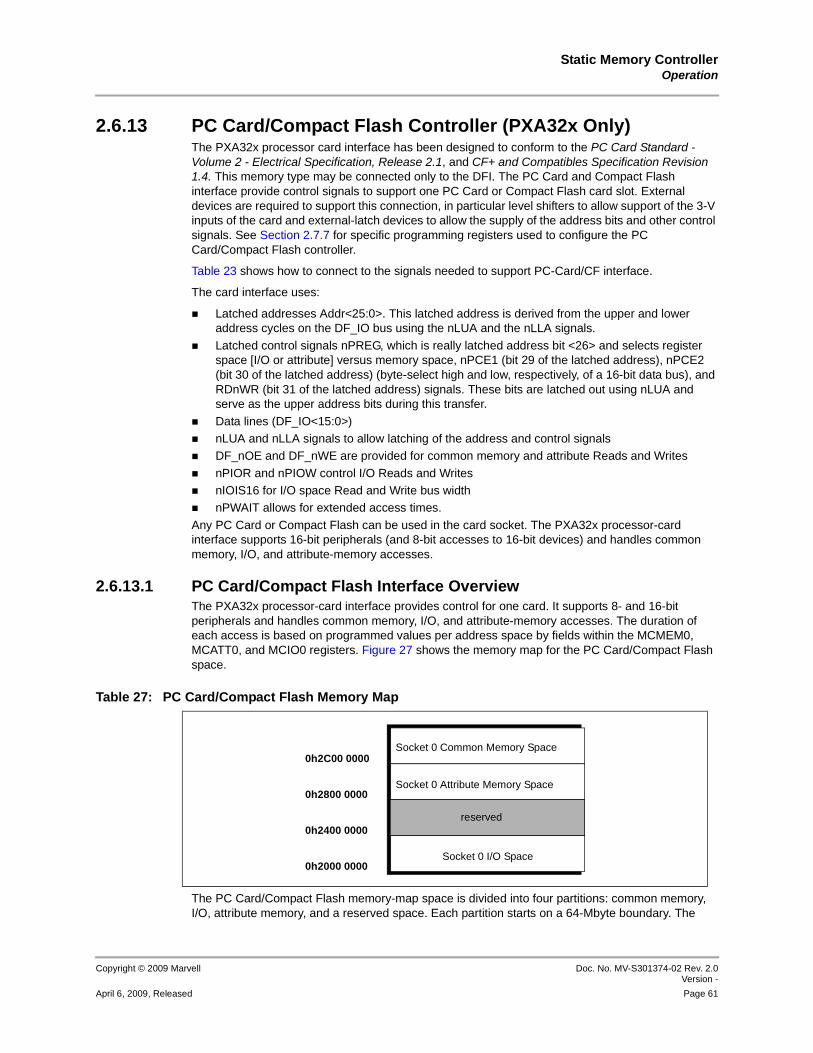
Static Memory ControllerOperation
Copyright © 2009 Marvell Doc. No. MV-S301374-02 Rev. 2.0Version -
April 6, 2009, Released Page 61
2.6.13 PC Card/Compact Flash Controller (PXA32x Only)The PXA32x processor card interface has been designed to conform to the PC Card Standard - Volume 2 - Electrical Specification, Release 2.1, and CF+ and Compatibles Specification Revision 1.4. This memory type may be connected only to the DFI. The PC Card and Compact Flash interface provide control signals to support one PC Card or Compact Flash card slot. External devices are required to support this connection, in particular level shifters to allow support of the 3-V inputs of the card and external-latch devices to allow the supply of the address bits and other control signals. See Section 2.7.7 for specific programming registers used to configure the PC Card/Compact Flash controller.
Table 23 shows how to connect to the signals needed to support PC-Card/CF interface.
The card interface uses:
Latched addresses Addr<25:0>. This latched address is derived from the upper and lower address cycles on the DF_IO bus using the nLUA and the nLLA signals.
Latched control signals nPREG, which is really latched address bit <26> and selects register space [I/O or attribute] versus memory space, nPCE1 (bit 29 of the latched address), nPCE2 (bit 30 of the latched address) (byte-select high and low, respectively, of a 16-bit data bus), and RDnWR (bit 31 of the latched address) signals. These bits are latched out using nLUA and serve as the upper address bits during this transfer.
Data lines (DF_IO<15:0>)nLUA and nLLA signals to allow latching of the address and control signals DF_nOE and DF_nWE are provided for common memory and attribute Reads and Writes
nPIOR and nPIOW control I/O Reads and WritesnIOIS16 for I/O space Read and Write bus widthnPWAIT allows for extended access times.
Any PC Card or Compact Flash can be used in the card socket. The PXA32x processor-card interface supports 16-bit peripherals (and 8-bit accesses to 16-bit devices) and handles common memory, I/O, and attribute-memory accesses.
2.6.13.1 PC Card/Compact Flash Interface OverviewThe PXA32x processor-card interface provides control for one card. It supports 8- and 16-bit peripherals and handles common memory, I/O, and attribute-memory accesses. The duration of each access is based on programmed values per address space by fields within the MCMEM0, MCATT0, and MCIO0 registers. Figure 27 shows the memory map for the PC Card/Compact Flash space.
The PC Card/Compact Flash memory-map space is divided into four partitions: common memory, I/O, attribute memory, and a reserved space. Each partition starts on a 64-Mbyte boundary. The
Table 27: PC Card/Compact Flash Memory Map
Socket 0 Common Memory Space
Socket 0 Attribute Memory Space
Socket 0 I/O Space
reserved
0h2C00 0000
0h2800 0000
0h2400 0000
0h2000 0000
PXA3xx (88AP3xx) Processor Family Vol. II: Memory Controller Configuration Developers Manual
Doc. No. MV-S301374-02 Rev. 2.0 Version -
Copyright © 2009 Marvell
Page 62 April 6, 2009, Released
address is driven out in two cycles using the LUA and LLA address cycles. The allocation of addresses to cycles is made according to Address Configuration Register P (CSADRCFG_P).
Several control signals are sent out on the LUA cycle. These are latched in the external latch devices. nPCE2, nPCE1, and RDnWR signals are sent on the upper address bits, which include bits 30, 29, and 31 of the latched address. In addition, the functionality of the nPREG signal from the PXA320 processor is provided using the relevant address bit.
For I/O accesses, the value of nPCE<2:1> depends on the value of nIOIS16, and thus is valid a finite time after nIOIS16 is valid. Because nIOIS16 depends on the address, a special mechanism is used to set the value correctly. Two nLUA address cycles are performed, one with address and an initial value of the nPCE bits with both asserted indicating a 16-bit transfer and a second after the nIOIS16 signal value is determined. The second address cycle has the identical address but has corrected nPCE bits. The Read or Write strobes are asserted as required only after this address cycle has been performed.
Common-memory and attribute-memory accesses assert the DF_nOE or DF_nWE control signals. I/O accesses assert the nPIOR or nPIOW control signals and use the nIOIS16 input signal to determine the bus width of the transfer (8 or 16 bits). The PXA320 processor uses nPCE2 to indicate to the expansion device that the upper half of the data bus, DF_IO<15:8>, is used for the transfer. nPCE1 indicates that the lower half of the data bus, DF_IO<7:0>, is used.
Attribute-memory space allows only even bytes for valid data, so the card ignores nPCE2 and the upper byte lane (odd byte), DF_IO<15:8>, and only looks at nPCE1 and the lower byte lane (even byte), DF_IO<7:0>. For this reason, no burst transfers should be performed to card-attribute memory space, that is, DMA, USB host, or LCD memory space. For common-memory and attribute-memory space, all even bytes are transferred across the lower byte lane, DF_IO<7:0>, with nPCE1 asserted. When nPCE1 and nPCE2 are asserted, address bit <0> is ignored, an even byte is transferred across DF_IO<7:0>, and an odd byte is transferred across DF_IO<15:8>. When nPCE2 is de-asserted and nPCE1 is asserted, address bit <0> is used to determine whether the byte being transferred across the lower byte lane is even (address bit <0> = 0) or odd (address bit <0> = 1). nPCE2 is never asserted when nPCE1 is de-asserted.
Accesses to I/O space may be 8- or 16-bits, depending on the state of the nIOIS16 input pin. I/O transfers always start assuming a 16-bit bus. After the address is placed on the bus, an I/O device may respond with nIOIS16, indicating that it can perform the transfer in a single 16-bit transfer. If nIOIS16 is not asserted within the proper time, the address is assumed to be to two 8-bit registers. The transfer is completed as two 8-bit transfers on the low byte lane, DF_IO<7:0>, with nPCE2 deasserted, nPCE1 asserted, address bit <0>=0 for the first 8-bit transfer (even byte), and address bit <0>=1 for the second 8-bit transfer (odd byte).
The memory controller waits indefinitely for the nPWAIT signal to be de-asserted, which can hang the system if the card memory is not responding. To prevent indefinite hangs, set the watchdog timer when starting a card transfer and the system reset, if no response is received from the card. The interface waits a minimum amount of time (<space>0_ASST_WAIT) before checking the value of the nPWAIT signal. If the nPWAIT signal is asserted (active low), the interface continues to wait for a variable number of wait states until nPWAIT is de-asserted. Once the nPWAIT signal is de-asserted, the command is asserted for a fixed amount of time (<space>0_ASST_HOLD).
For Writes to card sockets, if a byte has been masked out using a byte enable internally, the Write does not occur at all on the external bus. For Reads, 16 bits (or one half-word) are always read from the socket, even if only one byte was requested. In some cases, based on internal-address alignment, four bytes may be read (or one word), even if only one byte was requested.
For both Reads and Writes from/to card devices, a special DMA mode exists that causes the address to not be incriminated to the card device. This mode allows port-type card devices to interface to the PXA3xx Processor Family. The special DMA mode is valid only for VLIO and card devices. Refer to the DMA chapter for more information. Table 28, Table 29, Table 30, Table 31, Table 32, Table 33, Table 34, and Table 35 describe possible memory and I/O space Read and Write commands.
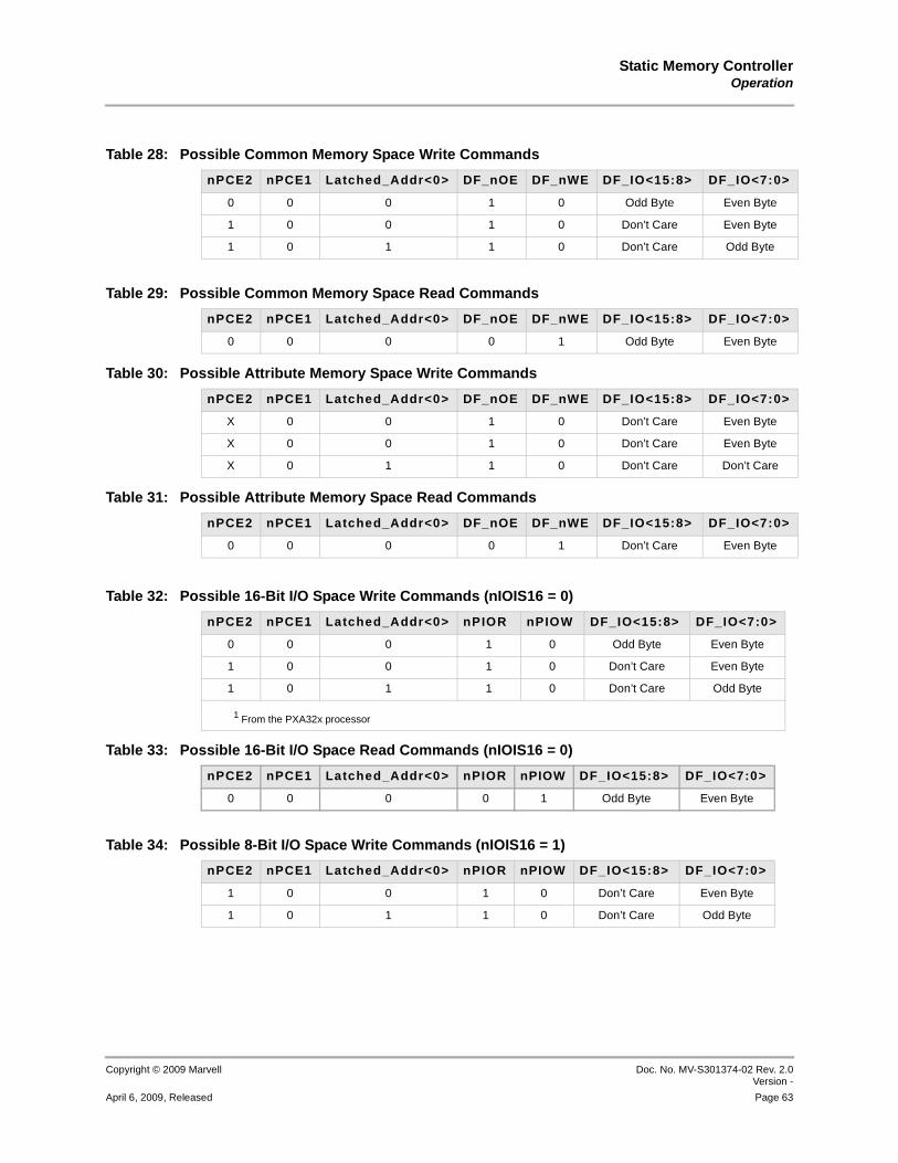
Static Memory ControllerOperation
Copyright © 2009 Marvell Doc. No. MV-S301374-02 Rev. 2.0Version -
April 6, 2009, Released Page 63
Table 28: Possible Common Memory Space Write Commands
nPCE2 nPCE1 Latched_Addr<0> DF_nOE DF_nWE DF_IO<15:8> DF_IO<7:0>
0 0 0 1 0 Odd Byte Even Byte
1 0 0 1 0 Don’t Care Even Byte
1 0 1 1 0 Don’t Care Odd Byte
Table 29: Possible Common Memory Space Read Commands
nPCE2 nPCE1 Latched_Addr<0> DF_nOE DF_nWE DF_IO<15:8> DF_IO<7:0>
0 0 0 0 1 Odd Byte Even Byte
Table 30: Possible Attribute Memory Space Write Commands
nPCE2 nPCE1 Latched_Addr<0> DF_nOE DF_nWE DF_IO<15:8> DF_IO<7:0>
X 0 0 1 0 Don’t Care Even Byte
X 0 0 1 0 Don’t Care Even Byte
X 0 1 1 0 Don’t Care Don’t Care
Table 31: Possible Attribute Memory Space Read Commands
nPCE2 nPCE1 Latched_Addr<0> DF_nOE DF_nWE DF_IO<15:8> DF_IO<7:0>
0 0 0 0 1 Don’t Care Even Byte
Table 32: Possible 16-Bit I/O Space Write Commands (nIOIS16 = 0)
nPCE2 nPCE1 Latched_Addr<0> nPIOR nPIOW DF_IO<15:8> DF_IO<7:0>
0 0 0 1 0 Odd Byte Even Byte
1 0 0 1 0 Don’t Care Even Byte
1 0 1 1 0 Don’t Care Odd Byte
1 From the PXA32x processor
Table 33: Possible 16-Bit I/O Space Read Commands (nIOIS16 = 0)
nPCE2 nPCE1 Latched_Addr<0> nPIOR nPIOW DF_IO<15:8> DF_IO<7:0>
0 0 0 0 1 Odd Byte Even Byte
Table 34: Possible 8-Bit I/O Space Write Commands (nIOIS16 = 1)
nPCE2 nPCE1 Latched_Addr<0> nPIOR nPIOW DF_IO<15:8> DF_IO<7:0>
1 0 0 1 0 Don’t Care Even Byte
1 0 1 1 0 Don’t Care Odd Byte
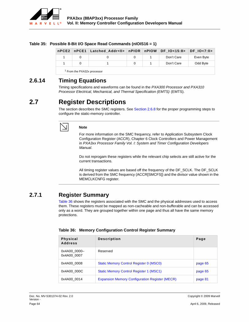
PXA3xx (88AP3xx) Processor Family Vol. II: Memory Controller Configuration Developers Manual
Doc. No. MV-S301374-02 Rev. 2.0 Version -
Copyright © 2009 Marvell
Page 64 April 6, 2009, Released
2.6.14 Timing Equations Timing specifications and waveforms can be found in the PXA300 Processor and PXA310 Processor Electrical, Mechanical, and Thermal Specification (EMTS) (EMTS).
2.7 Register DescriptionsThe section describes the SMC registers. See Section 2.6.8 for the proper programming steps to configure the static-memory controller.
Note
Note For more information on the SMC frequency, refer to Application Subsystem Clock Configuration Register (ACCR), Chapter 6 Clock Controllers and Power Management in PXA3xx Processor Family Vol. I: System and Timer Configuration Developers Manual.
Do not reprogam these registers while the relevant chip selects are still active for the current transactions.
All timing register values are based off the frequency of the DF_SCLK. The DF_SCLK is derived from the SMC frequency (ACCR[SMCFS]) and the divisor value shown in the MEMCLKCNFG register.
2.7.1 Register SummaryTable 36 shows the registers associated with the SMC and the physical addresses used to access them. These registers must be mapped as non-cacheable and non-bufferable and can be accessed only as a word. They are grouped together within one page and thus all have the same memory protections.
Table 35: Possible 8-Bit I/O Space Read Commands (nIOIS16 = 1)
nPCE2 nPCE1 Latched_Addr<0> nPIOR nPIOW DF_IO<15:8> DF_IO<7:0>
1 0 0 0 1 Don’t Care Even Byte
1 0 1 0 1 Don’t Care Odd Byte
1 From the PXA32x processor
Table 36: Memory Configuration Control Register Summary
Physical Address
Descript ion Page
0x4A00_0000–0x4A00_0007
Reserved
0x4A00_0008 Static Memory Control Register 0 (MSC0) page 65
0x4A00_000C Static Memory Control Register 1 (MSC1) page 65
0x4A00_0014 Expansion Memory Configuration Register (MECR) page 81
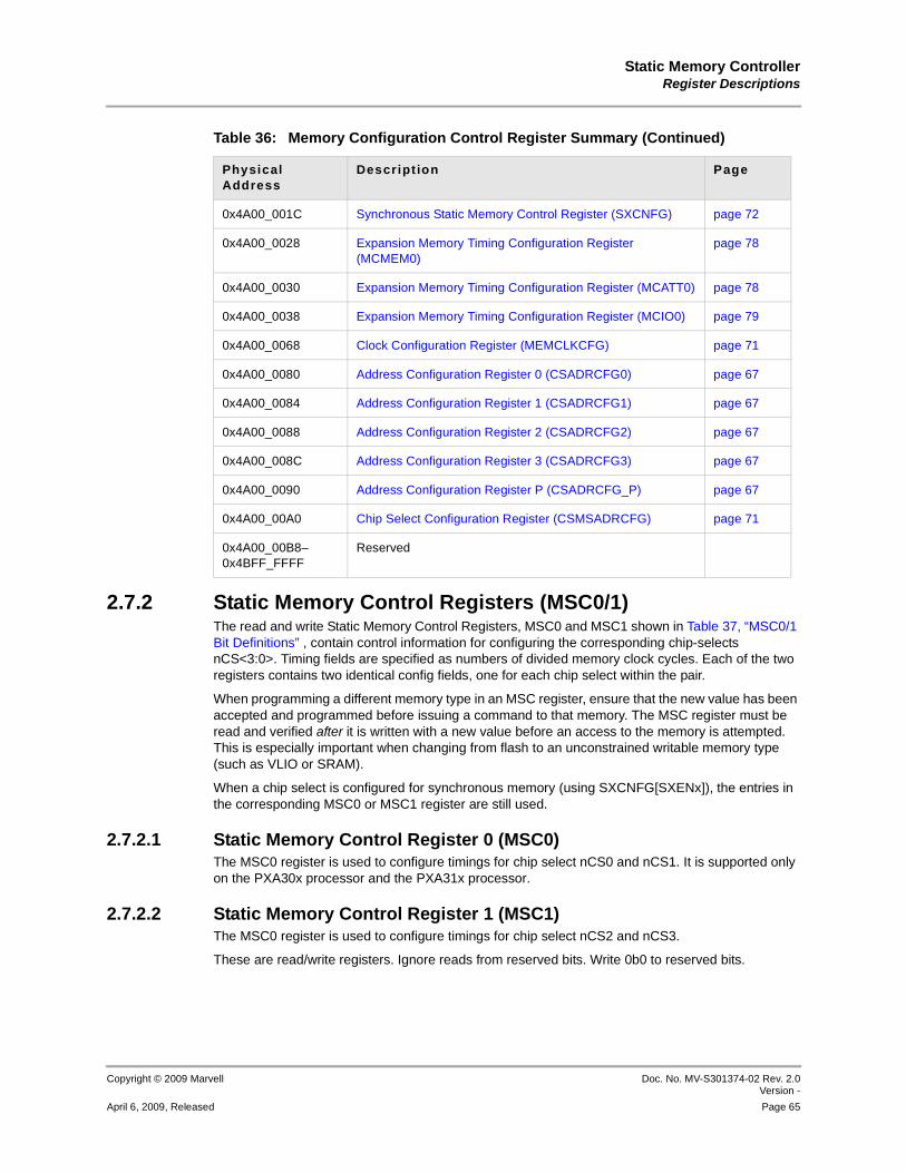
Static Memory ControllerRegister Descriptions
Copyright © 2009 Marvell Doc. No. MV-S301374-02 Rev. 2.0Version -
April 6, 2009, Released Page 65
2.7.2 Static Memory Control Registers (MSC0/1)The read and write Static Memory Control Registers, MSC0 and MSC1 shown in Table 37, “MSC0/1 Bit Definitions” , contain control information for configuring the corresponding chip-selects nCS<3:0>. Timing fields are specified as numbers of divided memory clock cycles. Each of the two registers contains two identical config fields, one for each chip select within the pair.
When programming a different memory type in an MSC register, ensure that the new value has been accepted and programmed before issuing a command to that memory. The MSC register must be read and verified after it is written with a new value before an access to the memory is attempted. This is especially important when changing from flash to an unconstrained writable memory type (such as VLIO or SRAM).
When a chip select is configured for synchronous memory (using SXCNFG[SXENx]), the entries in the corresponding MSC0 or MSC1 register are still used.
2.7.2.1 Static Memory Control Register 0 (MSC0)The MSC0 register is used to configure timings for chip select nCS0 and nCS1. It is supported only on the PXA30x processor and the PXA31x processor.
2.7.2.2 Static Memory Control Register 1 (MSC1)The MSC0 register is used to configure timings for chip select nCS2 and nCS3.
These are read/write registers. Ignore reads from reserved bits. Write 0b0 to reserved bits.
0x4A00_001C Synchronous Static Memory Control Register (SXCNFG) page 72
0x4A00_0028 Expansion Memory Timing Configuration Register (MCMEM0)
page 78
0x4A00_0030 Expansion Memory Timing Configuration Register (MCATT0) page 78
0x4A00_0038 Expansion Memory Timing Configuration Register (MCIO0) page 79
0x4A00_0068 Clock Configuration Register (MEMCLKCFG) page 71
0x4A00_0080 Address Configuration Register 0 (CSADRCFG0) page 67
0x4A00_0084 Address Configuration Register 1 (CSADRCFG1) page 67
0x4A00_0088 Address Configuration Register 2 (CSADRCFG2) page 67
0x4A00_008C Address Configuration Register 3 (CSADRCFG3) page 67
0x4A00_0090 Address Configuration Register P (CSADRCFG_P) page 67
0x4A00_00A0 Chip Select Configuration Register (CSMSADRCFG) page 71
0x4A00_00B8–0x4BFF_FFFF
Reserved
Table 36: Memory Configuration Control Register Summary (Continued)
Physical Address
Descript ion Page

PXA3xx (88AP3xx) Processor Family Vol. II: Memory Controller Configuration Developers Manual
Doc. No. MV-S301374-02 Rev. 2.0 Version -
Copyright © 2009 Marvell
Page 66 April 6, 2009, Released
Table 37: MSC0/1 Bit Definitions
Physical Address0x4A00_00080x4A00_000C
MSC0MSC1
Stat ic Memory Controller
User Settings
Bit 31 30 29 28 27 26 25 24 23 22 21 20 19 18 17 16 15 14 13 12 11 10 9 8 7 6 5 4 3 2 1 0
PX
A3
2x
pro
ce
ss
or
on
ly
Re
se
rve
d
RD
N3
RD
F3
RB
W3
RT
3
Re
se
rve
d
RD
N2
RD
F2
RB
W2
RT
2
PX
A3
0x
pro
ce
ss
or
an
dP
XA
31
x p
roc
es
so
r o
nly
Re
se
rve
d
RD
N1
/3
RD
F1
/3
Se
tAlw
ay
s
RT
1/3
Re
se
rve
d
RD
N0
/2
RD
F0
/2
Se
tAlw
ay
s
RT
0/2
Reset ? ? ? ? 1 1 1 1 1 1 1 1 0 0 0 0 ? ? ? ? 1 1 1 1 1 1 1 1 0 0 0 0
Bits Access Name Descript ion
31:28 and
15:12
— — Reserved
27:24 and11:8
R/W RDNx Return Delay Next is a programmable number of DF_SCLK cycles and varies for each interface type. • For SRAM accesses this is used to set the DF_nWE assertion time.• For VLIO accesses this is used to program setup and hold times in
relation to the DF_nWE and DF_nOE signals.• Not used for flash accesses.NOTE: Consult the PXA300 Processor and PXA310 Processor
Electrical, Mechanical, and Thermal Specification (EMTS) for specific usage based on interface type.
23:20 and7:4
R/W RDFx Return Delay First is a programmable number of DF_SCLK cycles and varies for each interface type. • For SRAM accesses this is used to set the DF_nOE assertion time
and to program the read data setup time.• For VLIO accesses this is used to set the DF_nWE and DF_nOE
assertion time• For Flash accesses this is used to set the DF_nWE and DF_nOE
assertion time and to program the read data setup time.NOTE: Consult the PXA300 Processor and PXA310 Processor
Electrical, Mechanical, and Thermal Specification (EMTS) for specific usage based on interface type.
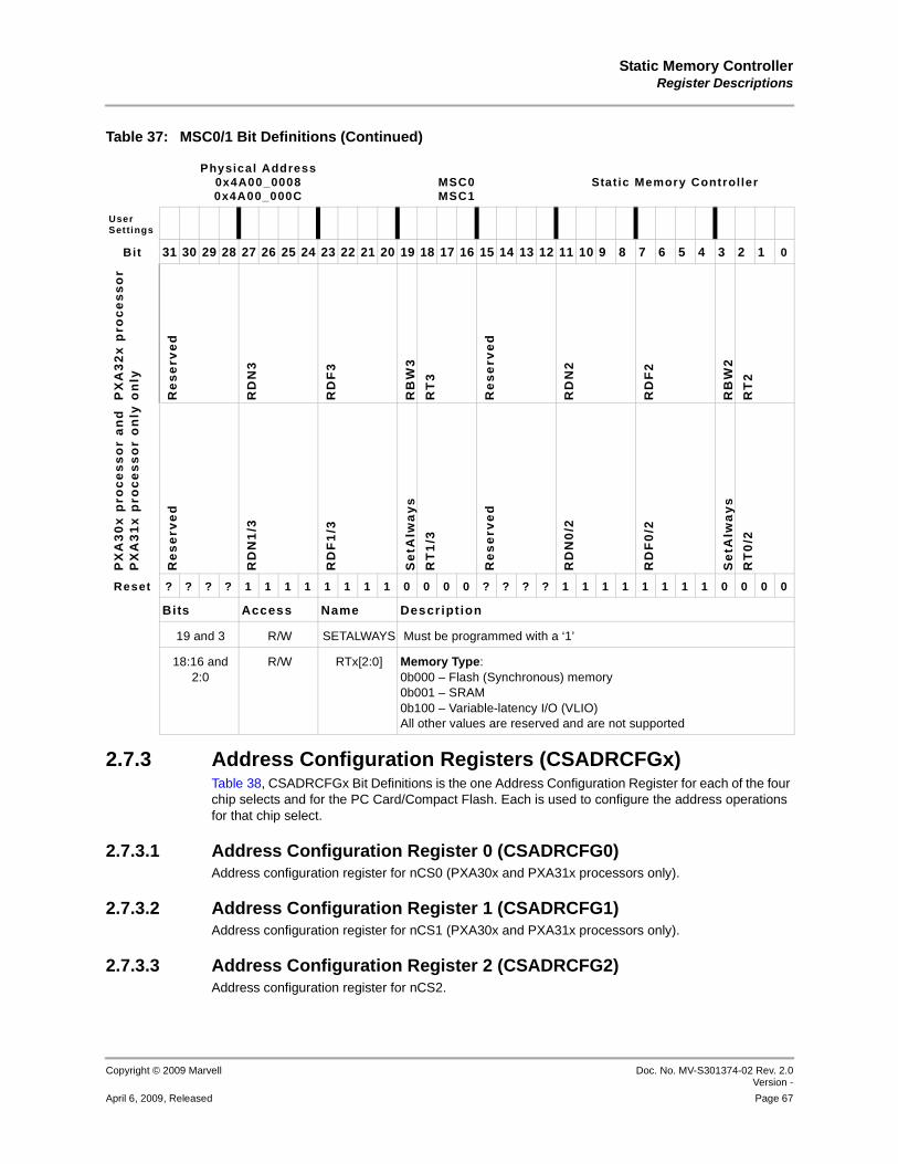
Static Memory ControllerRegister Descriptions
Copyright © 2009 Marvell Doc. No. MV-S301374-02 Rev. 2.0Version -
April 6, 2009, Released Page 67
2.7.3 Address Configuration Registers (CSADRCFGx)Table 38, CSADRCFGx Bit Definitions is the one Address Configuration Register for each of the four chip selects and for the PC Card/Compact Flash. Each is used to configure the address operations for that chip select.
2.7.3.1 Address Configuration Register 0 (CSADRCFG0)Address configuration register for nCS0 (PXA30x and PXA31x processors only).
2.7.3.2 Address Configuration Register 1 (CSADRCFG1)Address configuration register for nCS1 (PXA30x and PXA31x processors only).
2.7.3.3 Address Configuration Register 2 (CSADRCFG2)Address configuration register for nCS2.
19 and 3 R/W SETALWAYS Must be programmed with a ‘1’
18:16 and 2:0
R/W RTx[2:0] Memory Type:0b000 – Flash (Synchronous) memory0b001 – SRAM0b100 – Variable-latency I/O (VLIO)All other values are reserved and are not supported
Table 37: MSC0/1 Bit Definitions (Continued)
Physical Address0x4A00_00080x4A00_000C
MSC0MSC1
Stat ic Memory Controller
User Settings
Bit 31 30 29 28 27 26 25 24 23 22 21 20 19 18 17 16 15 14 13 12 11 10 9 8 7 6 5 4 3 2 1 0
PX
A3
2x
pro
ce
ss
or
on
ly
Re
se
rve
d
RD
N3
RD
F3
RB
W3
RT
3
Re
se
rve
d
RD
N2
RD
F2
RB
W2
RT
2
PX
A3
0x
pro
ce
ss
or
an
dP
XA
31
x p
roc
es
so
r o
nly
Re
se
rve
d
RD
N1
/3
RD
F1
/3
Se
tAlw
ay
s
RT
1/3
Re
se
rve
d
RD
N0
/2
RD
F0
/2
Se
tAlw
ay
s
RT
0/2
Reset ? ? ? ? 1 1 1 1 1 1 1 1 0 0 0 0 ? ? ? ? 1 1 1 1 1 1 1 1 0 0 0 0
Bits Access Name Descript ion

PXA3xx (88AP3xx) Processor Family Vol. II: Memory Controller Configuration Developers Manual
Doc. No. MV-S301374-02 Rev. 2.0 Version -
Copyright © 2009 Marvell
Page 68 April 6, 2009, Released
2.7.3.4 Address Configuration Register 3 (CSADRCFG3)Address configuration register for nCS3.
2.7.3.5 Address Configuration Register P (CSADRCFG_P)Address configuration register for PC Card/Compact Flash (PXA32x processor only).
These are read/write registers. Ignore reads from reserved bits. Write 0b0 to reserved bits.
Table 38: CSADRCFGx Bit Definitions
Physical Address0x4A00_00800x4A00_00840x4A00_00880x4A00_008C0x4A00_0090
CSADRCFG0CSADRCFG1CSADRCFG2CSADRCFG3CSADRCFG_P
Stat ic Memory Controller
User Settings
Bit 31 30 29 28 27 26 25 24 23 22 21 20 19 18 17 16 15 14 13 12 11 10 9 8 7 6 5 4 3 2 1 0
Reserved ALT ALWA
DD
RC
ON
FIG
Re
se
rve
d
AD
DR
SP
LIT
Re
se
rve
d
AD
DR
BA
SE
INF
TY
PE
Reset ? ? ? ? ? ? ? ? ? ? 0 0 0 0 1 0 0 0 ? ? 0 0 0 0 ? ? 0 0 0 0 0 0
Bits Access Name Description
31:22 — — Reserved
21:20 R/W ALT Address Latch Timing:Used to set the timing for an address to be valid on the DF_IO<15:0> bus with respect to the nLUA and nLLA signals..0b00 – No setup or hold is provided. • The address is sent out at the same time as the LxA signal is
asserted and removed at the same time as the signal is deasserted.
0b01 – No setup and one hold provided. • One DF_SCLK of hold is provided after the deassertion of the nLxA
signals.0b10 – No hold and one setup provided. • One DF_SCLK of setup is provided before the assertion of the
nLxA signals.0b11 – One setup and one hold is provided• One DF_SCLK setup and one hold.
NOTE: For asynchronous flash, hold time is in general required on the address so 0b01 or 0b11 are normally required. For synchronous reads and writes, an extra cycle of hold does not affect the latency to the read or write. The latency is the address valid signal latched to valid data on the bus.

Static Memory ControllerRegister Descriptions
Copyright © 2009 Marvell Doc. No. MV-S301374-02 Rev. 2.0Version -
April 6, 2009, Released Page 69
19:17 R/W ALW Address Latch Width:Used to set the width of the nLUA and nLLA signalsALW is the number of external DF_SCLK cycles that the nLUA and nLLA signals are asserted.0b000 is an illegal combination in all cases.NOTE: For all synchronous devices, this field MUST be configured to
0b001.
16:14 R/W ADDRCONFIG
Address Configuration:Controls the addressing mode during the upper and lower address cycles.0b000 - 0b001 – Full-latch mode0b011 – Low-order addressing in operationAll other values are reserved and are not supportedRefer to Section 2.6.7.1 for more information.
13:12 — — Reserved
11:8 R/W ADDRSPLIT Address Split:This configures the split point between the upper and lower address cycle. This selects the first address bit in the upper address cycle (nLUA)0b1000 – byte address bit 160b1001 – byte address bit 17All other values are reserved and are not supportedNOTE: Setting this field to b1001 is the general guideline to follow
7:6 — — Reserved
5:4 R/W ADDRBASE Address Base:The least significant address to be sent out as part of the lower address cycle.0b00 – Byte address bit <0> (Byte Addressing)0b01 – Byte address bit <1> (Word (x16) Addressing)0b10 – 0b11 – ReservedNOTE: Setting this field to b01 is the guideline to follow:
Table 38: CSADRCFGx Bit Definitions (Continued)
Physical Address0x4A00_00800x4A00_00840x4A00_00880x4A00_008C0x4A00_0090
CSADRCFG0CSADRCFG1CSADRCFG2CSADRCFG3CSADRCFG_P
Stat ic Memory Controller
User Settings
Bit 31 30 29 28 27 26 25 24 23 22 21 20 19 18 17 16 15 14 13 12 11 10 9 8 7 6 5 4 3 2 1 0
Reserved ALT ALW
AD
DR
CO
NF
IG
Re
se
rve
d
AD
DR
SP
LIT
Re
se
rve
d
AD
DR
BA
SE
INF
TY
PE
Reset ? ? ? ? ? ? ? ? ? ? 0 0 0 0 1 0 0 0 ? ? 0 0 0 0 ? ? 0 0 0 0 0 0
Bits Access Name Description
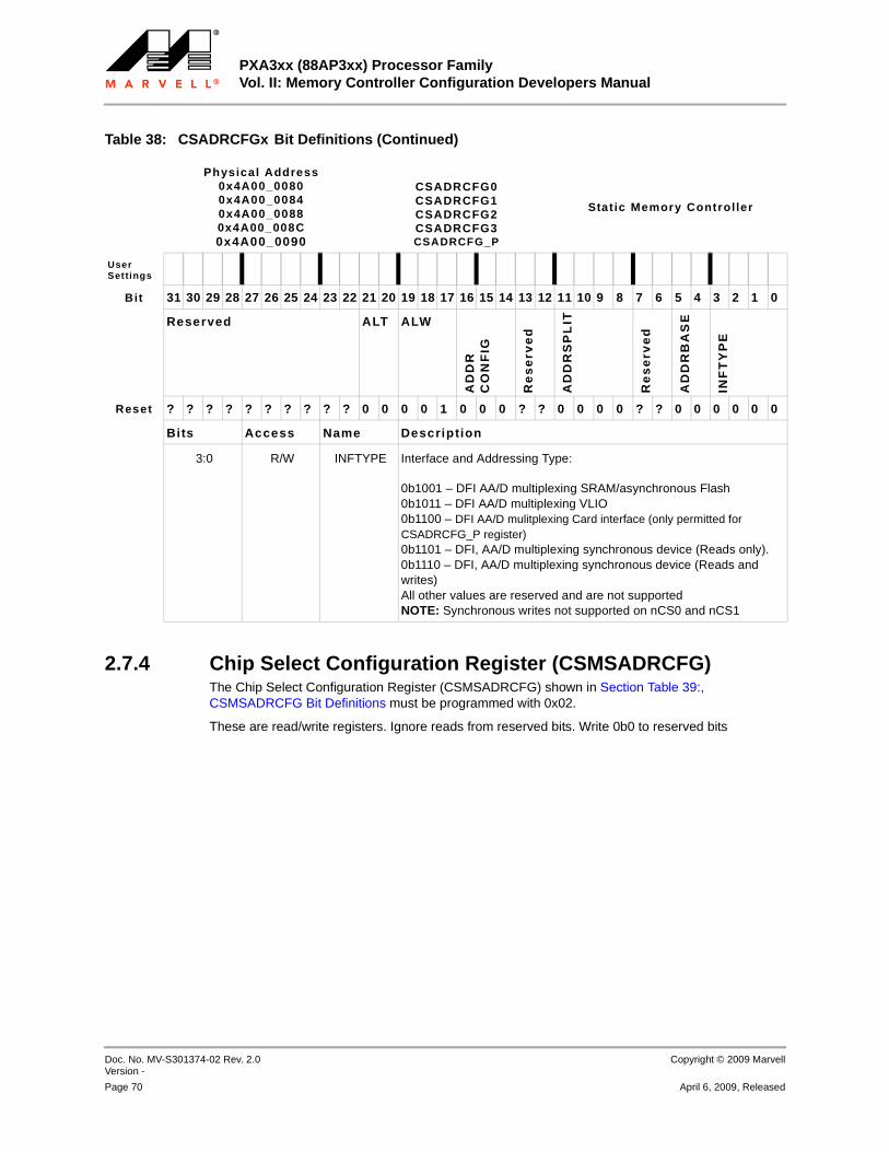
PXA3xx (88AP3xx) Processor Family Vol. II: Memory Controller Configuration Developers Manual
Doc. No. MV-S301374-02 Rev. 2.0 Version -
Copyright © 2009 Marvell
Page 70 April 6, 2009, Released
2.7.4 Chip Select Configuration Register (CSMSADRCFG)The Chip Select Configuration Register (CSMSADRCFG) shown in Section Table 39:, CSMSADRCFG Bit Definitions must be programmed with 0x02.
These are read/write registers. Ignore reads from reserved bits. Write 0b0 to reserved bits
3:0 R/W INFTYPE Interface and Addressing Type:
0b1001 – DFI AA/D multiplexing SRAM/asynchronous Flash0b1011 – DFI AA/D multiplexing VLIO0b1100 – DFI AA/D mulitplexing Card interface (only permitted for CSADRCFG_P register)0b1101 – DFI, AA/D multiplexing synchronous device (Reads only). 0b1110 – DFI, AA/D multiplexing synchronous device (Reads and writes) All other values are reserved and are not supportedNOTE: Synchronous writes not supported on nCS0 and nCS1
Table 38: CSADRCFGx Bit Definitions (Continued)
Physical Address0x4A00_00800x4A00_00840x4A00_00880x4A00_008C0x4A00_0090
CSADRCFG0CSADRCFG1CSADRCFG2CSADRCFG3CSADRCFG_P
Stat ic Memory Controller
User Settings
Bit 31 30 29 28 27 26 25 24 23 22 21 20 19 18 17 16 15 14 13 12 11 10 9 8 7 6 5 4 3 2 1 0
Reserved ALT ALW
AD
DR
CO
NF
IG
Re
se
rve
d
AD
DR
SP
LIT
Re
se
rve
d
AD
DR
BA
SE
INF
TY
PE
Reset ? ? ? ? ? ? ? ? ? ? 0 0 0 0 1 0 0 0 ? ? 0 0 0 0 ? ? 0 0 0 0 0 0
Bits Access Name Description

Static Memory ControllerRegister Descriptions
Copyright © 2009 Marvell Doc. No. MV-S301374-02 Rev. 2.0Version -
April 6, 2009, Released Page 71
Table 39: CSMSADRCFG Bit Definitions
Physical Address0x4A00_00A0
CSMSADRCFG Static Memory Controller
User Settings
Bit 31 30 29 28 27 26 25 24 23 22 21 20 19 18 17 16 15 14 13 12 11 10 9 8 7 6 5 4 3 2 1 0
Reserved
SE
TA
LW
AY
S
Re
se
rve
d
Reset ? ? ? ? ? ? ? ? ? ? ? ? ? ? ? ? ? ? ? ? ? ? ? ? ? ? ? ? ? ? 0 0
Bits Access Name Descript ion
31:2 — — Reserved
1 R/W SETALWAYS must be programmed to 0b1
0 R/W — Reserved
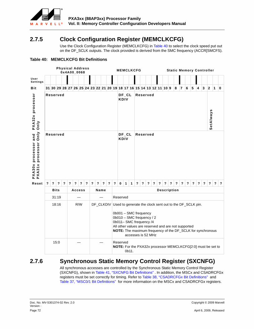
PXA3xx (88AP3xx) Processor Family Vol. II: Memory Controller Configuration Developers Manual
Doc. No. MV-S301374-02 Rev. 2.0 Version -
Copyright © 2009 Marvell
Page 72 April 6, 2009, Released
2.7.5 Clock Configuration Register (MEMCLKCFG)Use the Clock Configuration Register (MEMCLKCFG) in Table 40 to select the clock speed put out on the DF_SCLK outputs. The clock provided is derived from the SMC frequency (ACCR[SMCFS).
2.7.6 Synchronous Static Memory Control Register (SXCNFG)All synchronous accesses are controlled by the Synchronous Static Memory Control Register (SXCNFG), shown in Table 41, “SXCNFG Bit Definitions” . In addition, the MSCx and CSADRCFGx registers must be set correctly for timing. Refer to Table 38, “CSADRCFGx Bit Definitions” and Table 37, “MSC0/1 Bit Definitions” for more information on the MSCx and CSADRCFGx registers.
Table 40: MEMCLKCFG Bit Definitions
Physical Address0x4A00_0068
MEMCLKCFG Static Memory Controller
User Settings
Bit 31 30 29 28 27 26 25 24 23 22 21 20 19 18 17 16 15 14 13 12 11 10 9 8 7 6 5 4 3 2 1 0
PX
A3
2x
pro
ce
ss
or
On
ly
Reserved DF_CLKDIV
Reserved
Se
tAlw
ay
s
PX
A3
0x
pro
ce
ss
or
an
dP
XA
31
x p
roc
es
so
r O
nly Reserved DF_CL
KDIVReserved
Reset ? ? ? ? ? ? ? ? ? ? ? ? ? 0 1 1 ? ? ? ? ? ? ? ? ? ? ? ? ? ? ? ?
Bits Access Name Descript ion
31:19 — — Reserved
18:16 R/W DF_CLKDIV Used to generate the clock sent out to the DF_SCLK pin.
0b001 – SMC frequency0b010 – SMC frequency / 20b011– SMC frequency /4All other values are reserved and are not supportedNOTE: The maximum frequency of the DF_SCLK for synchronous
accesses is 52 MHz
15:0 — — ReservedNOTE: For the PXA32x processor MEMCLKCFG[2:0] must be set to
0b11.
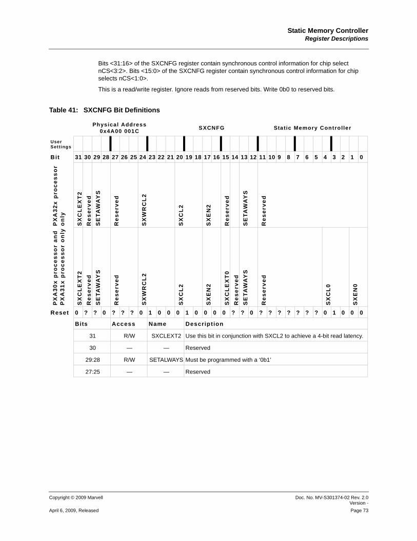
Static Memory ControllerRegister Descriptions
Copyright © 2009 Marvell Doc. No. MV-S301374-02 Rev. 2.0Version -
April 6, 2009, Released Page 73
Bits <31:16> of the SXCNFG register contain synchronous control information for chip select nCS<3:2>. Bits <15:0> of the SXCNFG register contain synchronous control information for chip selects nCS<1:0>.
This is a read/write register. Ignore reads from reserved bits. Write 0b0 to reserved bits.
Table 41: SXCNFG Bit Definitions
Physical Address0x4A00 001C
SXCNFG Static Memory Controller
User Settings
Bit 31 30 29 28 27 26 25 24 23 22 21 20 19 18 17 16 15 14 13 12 11 10 9 8 7 6 5 4 3 2 1 0
PX
A3
2x
pro
ce
ss
or
on
ly
SX
CL
EX
T2
Re
se
rve
d
SE
TA
WA
YS
Re
se
rve
d
SX
WR
CL
2
SX
CL
2
SX
EN
2
Re
se
rve
d
SE
TA
WA
YS
Re
se
rve
d
PX
A3
0x
pro
ce
ss
or
an
dP
XA
31
x p
roc
es
so
r o
nly
SX
CL
EX
T2
Re
se
rve
d
SE
TA
WA
YS
Re
se
rve
d
SX
WR
CL
2
SX
CL
2
SX
EN
2
SX
CL
EX
T0
Re
se
rve
d
SE
TA
WA
YS
Re
se
rve
d
SX
CL
0
SX
EN
0
Reset 0 ? ? 0 ? ? ? 0 1 0 0 0 1 0 0 0 0 ? ? 0 ? ? ? ? ? ? ? 0 1 0 0 0
Bits Access Name Descript ion
31 R/W SXCLEXT2 Use this bit in conjunction with SXCL2 to achieve a 4-bit read latency.
30 — — Reserved
29:28 R/W SETALWAYS Must be programmed with a ‘0b1’
27:25 — — Reserved
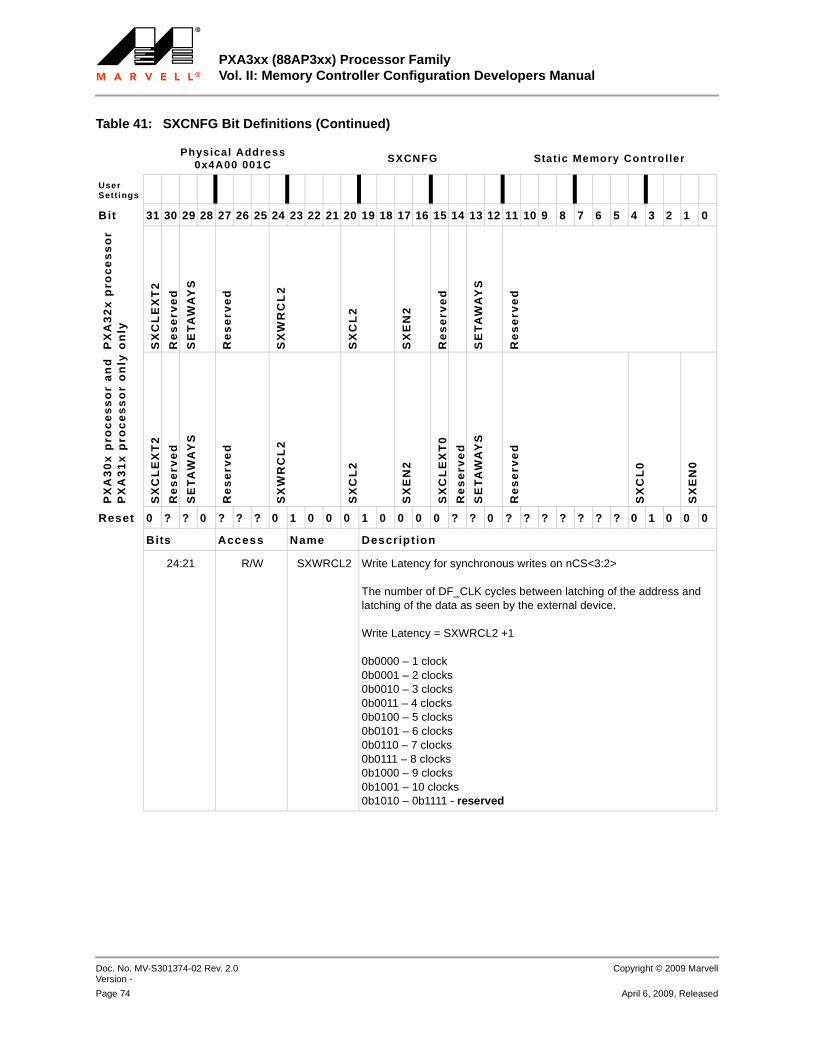
PXA3xx (88AP3xx) Processor Family Vol. II: Memory Controller Configuration Developers Manual
Doc. No. MV-S301374-02 Rev. 2.0 Version -
Copyright © 2009 Marvell
Page 74 April 6, 2009, Released
24:21 R/W SXWRCL2 Write Latency for synchronous writes on nCS<3:2>
The number of DF_CLK cycles between latching of the address and latching of the data as seen by the external device.
Write Latency = SXWRCL2 +1
0b0000 – 1 clock0b0001 – 2 clocks0b0010 – 3 clocks0b0011 – 4 clocks0b0100 – 5 clocks0b0101 – 6 clocks0b0110 – 7 clocks0b0111 – 8 clocks0b1000 – 9 clocks0b1001 – 10 clocks0b1010 – 0b1111 - reserved
Table 41: SXCNFG Bit Definitions (Continued)
Physical Address0x4A00 001C
SXCNFG Static Memory Controller
User Settings
Bit 31 30 29 28 27 26 25 24 23 22 21 20 19 18 17 16 15 14 13 12 11 10 9 8 7 6 5 4 3 2 1 0
PX
A3
2x
pro
ce
ss
or
on
ly
SX
CL
EX
T2
Re
se
rve
d
SE
TA
WA
YS
Re
se
rve
d
SX
WR
CL
2
SX
CL
2
SX
EN
2
Re
se
rve
d
SE
TA
WA
YS
Re
se
rve
d
PX
A3
0x
pro
ce
ss
or
an
dP
XA
31
x p
roc
es
so
r o
nly
SX
CL
EX
T2
Re
se
rve
d
SE
TA
WA
YS
Re
se
rve
d
SX
WR
CL
2
SX
CL
2
SX
EN
2
SX
CL
EX
T0
Re
se
rve
d
SE
TA
WA
YS
Re
se
rve
d
SX
CL
0
SX
EN
0
Reset 0 ? ? 0 ? ? ? 0 1 0 0 0 1 0 0 0 0 ? ? 0 ? ? ? ? ? ? ? 0 1 0 0 0
Bits Access Name Descript ion
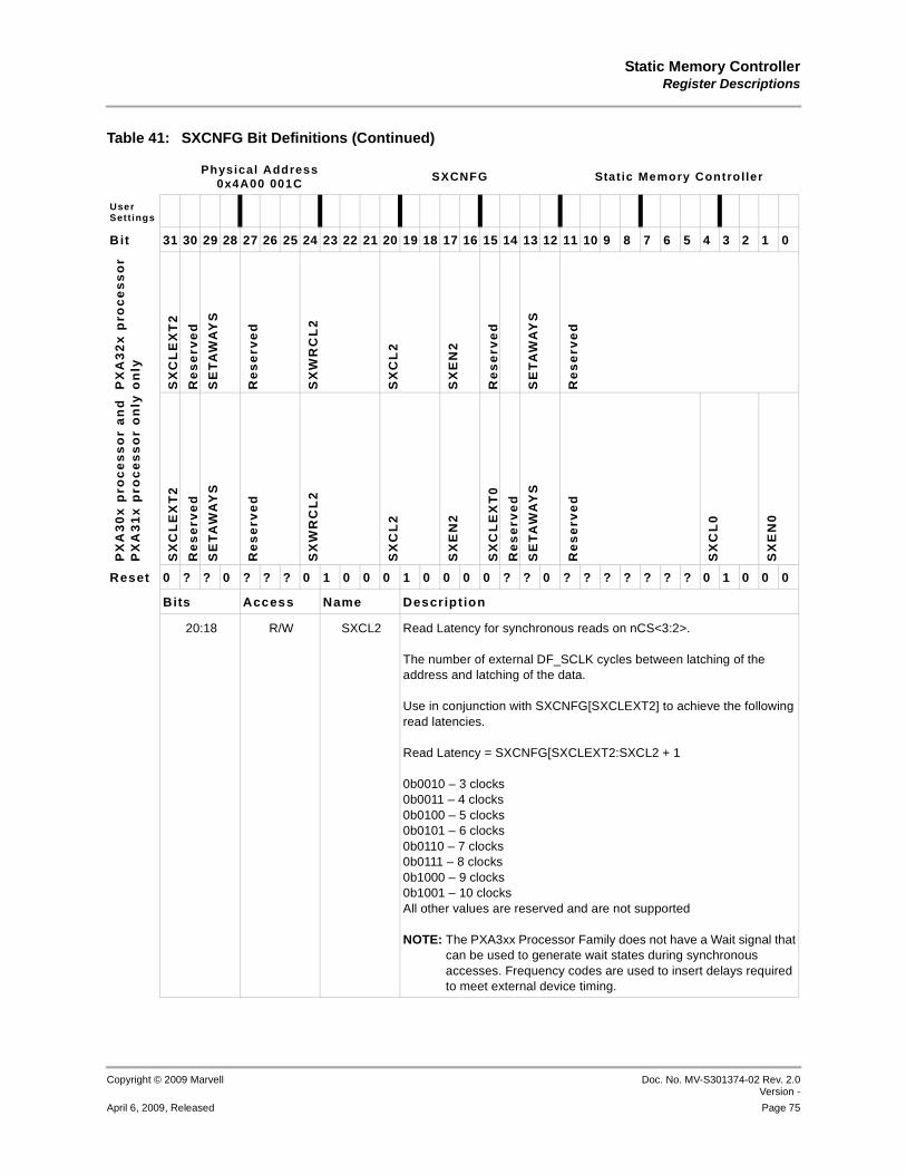
Static Memory ControllerRegister Descriptions
Copyright © 2009 Marvell Doc. No. MV-S301374-02 Rev. 2.0Version -
April 6, 2009, Released Page 75
20:18 R/W SXCL2 Read Latency for synchronous reads on nCS<3:2>.
The number of external DF_SCLK cycles between latching of the address and latching of the data.
Use in conjunction with SXCNFG[SXCLEXT2] to achieve the following read latencies.
Read Latency = SXCNFG[SXCLEXT2:SXCL2 + 1
0b0010 – 3 clocks 0b0011 – 4 clocks0b0100 – 5 clocks0b0101 – 6 clocks0b0110 – 7 clocks 0b0111 – 8 clocks0b1000 – 9 clocks 0b1001 – 10 clocks All other values are reserved and are not supported
NOTE: The PXA3xx Processor Family does not have a Wait signal that can be used to generate wait states during synchronous accesses. Frequency codes are used to insert delays required to meet external device timing.
Table 41: SXCNFG Bit Definitions (Continued)
Physical Address0x4A00 001C
SXCNFG Static Memory Controller
User Settings
Bit 31 30 29 28 27 26 25 24 23 22 21 20 19 18 17 16 15 14 13 12 11 10 9 8 7 6 5 4 3 2 1 0
PX
A3
2x
pro
ce
ss
or
on
ly
SX
CL
EX
T2
Re
se
rve
d
SE
TA
WA
YS
Re
se
rve
d
SX
WR
CL
2
SX
CL
2
SX
EN
2
Re
se
rve
d
SE
TA
WA
YS
Re
se
rve
d
PX
A3
0x
pro
ce
ss
or
an
dP
XA
31
x p
roc
es
so
r o
nly
SX
CL
EX
T2
Re
se
rve
d
SE
TA
WA
YS
Re
se
rve
d
SX
WR
CL
2
SX
CL
2
SX
EN
2
SX
CL
EX
T0
Re
se
rve
d
SE
TA
WA
YS
Re
se
rve
d
SX
CL
0
SX
EN
0
Reset 0 ? ? 0 ? ? ? 0 1 0 0 0 1 0 0 0 0 ? ? 0 ? ? ? ? ? ? ? 0 1 0 0 0
Bits Access Name Descript ion
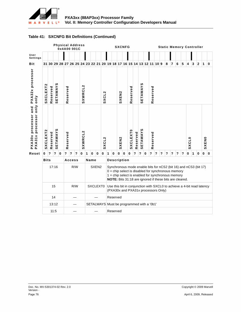
PXA3xx (88AP3xx) Processor Family Vol. II: Memory Controller Configuration Developers Manual
Doc. No. MV-S301374-02 Rev. 2.0 Version -
Copyright © 2009 Marvell
Page 76 April 6, 2009, Released
17:16 R/W SXEN2 Synchronous mode enable bits for nCS2 (bit 16) and nCS3 (bit 17)0 = chip select is disabled for synchronous memory1 = chip select is enabled for synchronous memoryNOTE: Bits 31:18 are ignored if these bits are cleared.
15 R/W SXCLEXT0 Use this bit in conjunction with SXCL0 to achieve a 4-bit read latency (PXA30x and PXA31x processors Only)
14 — — Reserved
13:12 — SETALWAYS Must be programmed with a ‘0b1’
11:5 — — Reserved
Table 41: SXCNFG Bit Definitions (Continued)
Physical Address0x4A00 001C
SXCNFG Static Memory Controller
User Settings
Bit 31 30 29 28 27 26 25 24 23 22 21 20 19 18 17 16 15 14 13 12 11 10 9 8 7 6 5 4 3 2 1 0
PX
A3
2x
pro
ce
ss
or
on
ly
SX
CL
EX
T2
Re
se
rve
d
SE
TA
WA
YS
Re
se
rve
d
SX
WR
CL
2
SX
CL
2
SX
EN
2
Re
se
rve
d
SE
TA
WA
YS
Re
se
rve
d
PX
A3
0x
pro
ce
ss
or
an
dP
XA
31
x p
roc
es
so
r o
nly
SX
CL
EX
T2
Re
se
rve
d
SE
TA
WA
YS
Re
se
rve
d
SX
WR
CL
2
SX
CL
2
SX
EN
2
SX
CL
EX
T0
Re
se
rve
d
SE
TA
WA
YS
Re
se
rve
d
SX
CL
0
SX
EN
0
Reset 0 ? ? 0 ? ? ? 0 1 0 0 0 1 0 0 0 0 ? ? 0 ? ? ? ? ? ? ? 0 1 0 0 0
Bits Access Name Descript ion
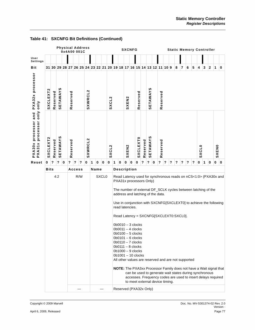
Static Memory ControllerRegister Descriptions
Copyright © 2009 Marvell Doc. No. MV-S301374-02 Rev. 2.0Version -
April 6, 2009, Released Page 77
4:2 R/W SXCL0 Read Latency used for synchronous reads on nCS<1:0> (PXA30x and PXA31x processors Only)
The number of external DF_SCLK cycles between latching of the address and latching of the data.
Use in conjunction with SXCNFG[SXCLEXT0] to achieve the following read latencies.
Read Latency = SXCNFG[SXCLEXT0:SXCL0].
0b0010 – 3 clocks 0b0011 – 4 clocks0b0100 – 5 clocks0b0101 – 6 clocks0b0110 – 7 clocks 0b0111 – 8 clocks0b1000 – 9 clocks 0b1001 – 10 clocks All other values are reserved and are not supported
NOTE: The PXA3xx Processor Family does not have a Wait signal that can be used to generate wait states during synchronous accesses. Frequency codes are used to insert delays required to meet external device timing.
— — Reserved (PXA32x Only)
Table 41: SXCNFG Bit Definitions (Continued)
Physical Address0x4A00 001C
SXCNFG Static Memory Controller
User Settings
Bit 31 30 29 28 27 26 25 24 23 22 21 20 19 18 17 16 15 14 13 12 11 10 9 8 7 6 5 4 3 2 1 0
PX
A3
2x
pro
ce
ss
or
on
ly
SX
CL
EX
T2
Re
se
rve
d
SE
TA
WA
YS
Re
se
rve
d
SX
WR
CL
2
SX
CL
2
SX
EN
2
Re
se
rve
d
SE
TA
WA
YS
Re
se
rve
d
PX
A3
0x
pro
ce
ss
or
an
dP
XA
31
x p
roc
es
so
r o
nly
SX
CL
EX
T2
Re
se
rve
d
SE
TA
WA
YS
Re
se
rve
d
SX
WR
CL
2
SX
CL
2
SX
EN
2
SX
CL
EX
T0
Re
se
rve
d
SE
TA
WA
YS
Re
se
rve
d
SX
CL
0
SX
EN
0
Reset 0 ? ? 0 ? ? ? 0 1 0 0 0 1 0 0 0 0 ? ? 0 ? ? ? ? ? ? ? 0 1 0 0 0
Bits Access Name Descript ion

PXA3xx (88AP3xx) Processor Family Vol. II: Memory Controller Configuration Developers Manual
Doc. No. MV-S301374-02 Rev. 2.0 Version -
Copyright © 2009 Marvell
Page 78 April 6, 2009, Released
2.7.7 Card Interface Registers (PXA32x processor only)This section describes the registers that must be programmed for PC Card and Compact Flash support.
The read/write registers MCMEM0, MCATT0, and MCIO0 contain control bits for configuring the timing of the PC Card/Compact Flash interface. When referring to these registers, the convention MC<space>0 is used, where <space> refers to memory, attribute, or I/O space.
The programming of each of the four fields in each of the three registers allows users to select the duration of accesses to I/O, common memory, and attribute space for the PC Card/Compact Flash card slot individually.
2.7.7.1 Expansion Memory Timing Configuration Register (MCMEM0)Configuration register for common memory for PC Card/Compact Flash accesses.
2.7.7.2 Expansion Memory Timing Configuration Register (MCATT0)Configuration register for attribute space for PC Card/Compact Flash accesses.
1:0 R/W SXEN0 Synchronous mode enable bits for nCS0 (bit 16) and nCS1 (bit 17) (PXA30x and PXA31x processors Only)0 = chip select is disabled for synchronous memory1 = chip select is enabled for synchronous memoryBits 15:2 are ignored if these bits are cleared.
— — Reserved (PXA32x Only)
Table 41: SXCNFG Bit Definitions (Continued)
Physical Address0x4A00 001C
SXCNFG Static Memory Controller
User Settings
Bit 31 30 29 28 27 26 25 24 23 22 21 20 19 18 17 16 15 14 13 12 11 10 9 8 7 6 5 4 3 2 1 0
PX
A3
2x
pro
ce
ss
or
on
ly
SX
CL
EX
T2
Re
se
rve
d
SE
TA
WA
YS
Re
se
rve
d
SX
WR
CL
2
SX
CL
2
SX
EN
2
Re
se
rve
d
SE
TA
WA
YS
Re
se
rve
d
PX
A3
0x
pro
ce
ss
or
an
dP
XA
31
x p
roc
es
so
r o
nly
SX
CL
EX
T2
Re
se
rve
d
SE
TA
WA
YS
Re
se
rve
d
SX
WR
CL
2
SX
CL
2
SX
EN
2
SX
CL
EX
T0
Re
se
rve
d
SE
TA
WA
YS
Re
se
rve
d
SX
CL
0
SX
EN
0
Reset 0 ? ? 0 ? ? ? 0 1 0 0 0 1 0 0 0 0 ? ? 0 ? ? ? ? ? ? ? 0 1 0 0 0
Bits Access Name Descript ion

Static Memory ControllerRegister Descriptions
Copyright © 2009 Marvell Doc. No. MV-S301374-02 Rev. 2.0Version -
April 6, 2009, Released Page 79
2.7.7.3 Expansion Memory Timing Configuration Register (MCIO0)Configuration register for Input/Output space for PC Card/Compact Flash accesses.
These are read/write registers. Ignore reads from reserved bits. Write 0b0 to reserved bits.
Table 42: MC<space>0 Bit Definitions
Physical Address0x4A00_00280x4A00_00300x4A00_0038
MCMEM0MCATT0MCIO0
Static Memory Control ler
User Settings
Bit 31 30 29 28 27 26 25 24 23 22 21 20 19 18 17 16 15 14 13 12 11 10 9 8 7 6 5 4 3 2 1 0
Reserved <space>0_HOLD
Re
se
rve
d <space>0_ASST
<space>0_SET
Reset ? ? ? ? ? ? ? ? ? ? ? ? 0 0 0 0 0 0 ? ? 0 0 0 0 0 0 0 0 0 0 0 0
Bits Access Name Descript ion
31:20 — — Reserved
19:14 R/W <space>0_HOLD
Number of memory clocks to hold address after command deassertion for <space> for socket. The lowest allowed value for this is 1 memory clock.
NOTE: Must be programmed to 01b or greater. 00b will result in 1 clock cycle.
13:12 — — Reserved
11:7 R/W <space>0_ASST Code for the command assertion time. See Table 43 for a description of this code and its effect on the command assertion.
6:0 R/W <space>0_SET
Number of memory clocks to setup address before command assertion for <space> for socket. The lowest allowed value for this is 1 memory clock.
NOTE: Must be programmed to 01b or greater. 00b will result in 1 clock cycle.
Table 43: Card Interface Command Assertion Codes
<space>0_ASST 0_ASST_WAIT_NPWAIT_SYNC
0_ASST_HOLD 0_ASST_WAIT +0_ASST_HOLD
Programmed Bit Value(Code)
Code Decimal Value (Code)
# DF_SCLKs before Checking nPWAIT_SYNC is Sampled for a ‘1’ (Code + 1)
# DF_SCLKs to Assert Command after nPWAIT=’1’(2*Code + 2)
# CLK_SMEMs for Minimum Command Assert ion Time(3*Code + 3)
00000 0 1 2 3
00001 1 2 4 6
00010 2 3 6 9
00011 3 4 8 12
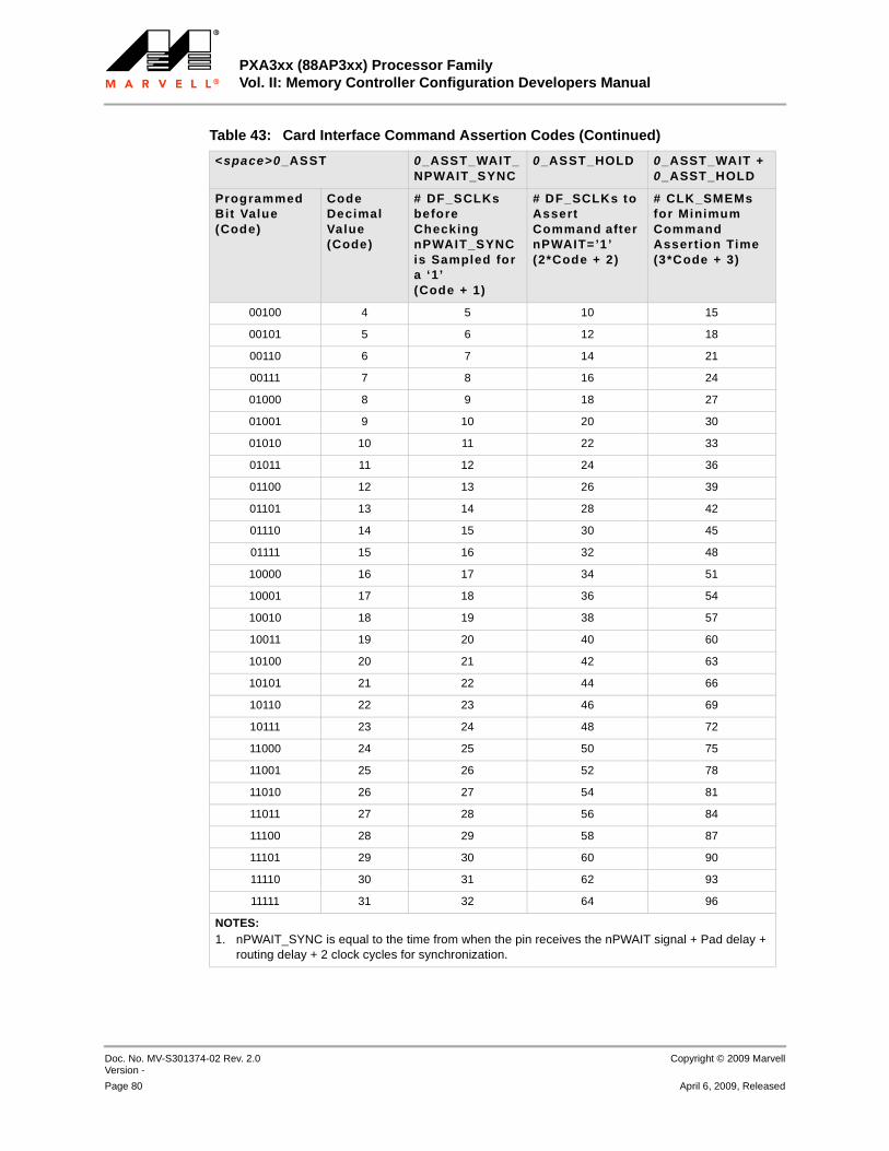
PXA3xx (88AP3xx) Processor Family Vol. II: Memory Controller Configuration Developers Manual
Doc. No. MV-S301374-02 Rev. 2.0 Version -
Copyright © 2009 Marvell
Page 80 April 6, 2009, Released
00100 4 5 10 15
00101 5 6 12 18
00110 6 7 14 21
00111 7 8 16 24
01000 8 9 18 27
01001 9 10 20 30
01010 10 11 22 33
01011 11 12 24 36
01100 12 13 26 39
01101 13 14 28 42
01110 14 15 30 45
01111 15 16 32 48
10000 16 17 34 51
10001 17 18 36 54
10010 18 19 38 57
10011 19 20 40 60
10100 20 21 42 63
10101 21 22 44 66
10110 22 23 46 69
10111 23 24 48 72
11000 24 25 50 75
11001 25 26 52 78
11010 26 27 54 81
11011 27 28 56 84
11100 28 29 58 87
11101 29 30 60 90
11110 30 31 62 93
11111 31 32 64 96
NOTES:1. nPWAIT_SYNC is equal to the time from when the pin receives the nPWAIT signal + Pad delay +
routing delay + 2 clock cycles for synchronization.
Table 43: Card Interface Command Assertion Codes (Continued)
<space>0_ASST 0_ASST_WAIT_NPWAIT_SYNC
0_ASST_HOLD 0_ASST_WAIT +0_ASST_HOLD
Programmed Bit Value(Code)
Code Decimal Value (Code)
# DF_SCLKs before Checking nPWAIT_SYNC is Sampled for a ‘1’ (Code + 1)
# DF_SCLKs to Assert Command after nPWAIT=’1’(2*Code + 2)
# CLK_SMEMs for Minimum Command Assert ion Time(3*Code + 3)
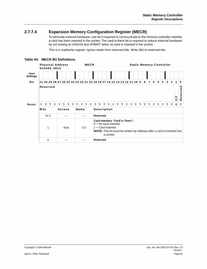
Static Memory ControllerRegister Descriptions
Copyright © 2009 Marvell Doc. No. MV-S301374-02 Rev. 2.0Version -
April 6, 2009, Released Page 81
2.7.7.4 Expansion Memory Configuration Register (MECR)To eliminate external hardware, one bit is required to communicate to the memory controller whether a card has been inserted in the socket. The card-is-there bit is required to reduce external hardware by not looking at nIOIS16 and nPWAIT when no card is inserted in the socket.
This is a read/write register. Ignore reads from reserved bits. Write 0b0 to reserved bits.
Table 44: MECR Bit Definitions
Physical Address0x4A00_0014
MECR Stat ic Memory Controller
User Settings
Bit 31 30 29 28 27 26 25 24 23 22 21 20 19 18 17 16 15 14 13 12 11 10 9 8 7 6 5 4 3 2 1 0
Reserved
CIT
Re
se
rve
d
Reset ? ? ? ? ? ? ? ? ? ? ? ? ? ? ? ? ? ? ? ? ? ? ? ? ? ? ? ? ? ? 0 ?
Bits Access Name Description
31:2 — — Reserved
1 R/W CIT
Card Interface “Card is There”:0 = No card inserted1 = Card insertedNOTE: This bit must be written by software after a card is inserted into
a socket.
0 — — Reserved
PXA3xx (88AP3xx) Processor Family Vol. II: Memory Controller Configuration Developers Manual
Doc. No. MV-S301374-02 Rev. 2.0 Version -
Copyright © 2009 Marvell
Page 82 April 6, 2009, Released

NAND Flash ControllerExternal Memory Pin Interface (EMPI)
Copyright © 2009 Marvell Doc. No. MV-S301374-02 Rev. 2.0Version -
April 6, 2009 Released Page 83
12345678910111213141516171819202122232425262728293031323334353637383940414243444546474849505152535455565758
3 NAND Flash ControllerThis chapter describes the PXA32x, PXA31x and PXA30x processors (referred to as “the processor” through this chapter) NAND Flash Controller (NFC) used to communicate to NAND memory. The usage model for the NAND flash memory is that of a mass storage for the processor. A flash file system (FFS) performs tasks such as wear leveling, garbage collection, and bad-block replacement for the flash media. The NFC accepts commands from the file system, controls the flash device according to these commands, and performs error control.
3.1 External Memory Pin Interface (EMPI)The EMPI is a 32-bit high-speed memory interface on the PXA32x processor, and a 16-bit high- speed memory interface on the PXA30x and PXA31x processors. The EMPI is also used by the Dynamic Memory Controller. The EMPI has all data and control signals required to interface to Double Data Rate (DDR) SDRAM.
3.1.1 Dynamic Memory Controller (DMC)The Dynamic Memory Controller (DMC) supports JEDEC-compliant Low Power Double Data Rate (DDR) SDRAM. Refer to the Dynamic Memory Controller chapter in this volume for more information on the DMC.
3.2 Data Flash Interface (DFI) The DFI is shared between the NAND Flash Controller (NFC) and the Static Memory Controller (SMC). It is a 16-bit interface with multiplexed address and data signals on the DF_IO<15:0> pins. Two sets of control signals are shared between the NFC and SMC.
Address Latch Enable (ALE) and Write Enable (nWE) on the DF_ALE_nWE pin.
Command Latch Enable (CLE) and Output Enable (nOE) on the DF_CLE_nOE pin
The NFC also has two additional control signals (Read Enable (nRE) and Write Enable (nWE)) that are not shared with the SMC. The NFC and SMC also have separate chip selects independent of each other.
3.2.1 NAND Flash Controller (NFC)The NAND Flash Controller (NFC) supports large- and small-block 8-bit and 16-bit NAND flash devices.
3.2.2 Static Memory Controller (SMC)The Static Memory Controller (SMC) maintains multiple static-memory types, such as synchronous and asynchronous flash devices, SRAM, SRAM-like variable-latency IO devices (VLIO) and compact Flash (PXA32x processor only). Refer to the Static Memory Controller chapter in this volume for more details on the SMC.
3.3 OverviewThe NFC provides an interface to NAND memory using the signals listed in Table 46, “NAND Flash Controller Signal Descriptions”. All of these signals are on multi-function pins that must be configured before using. The Multi-Functional Pin Registers (MFPR) and alternate functions are
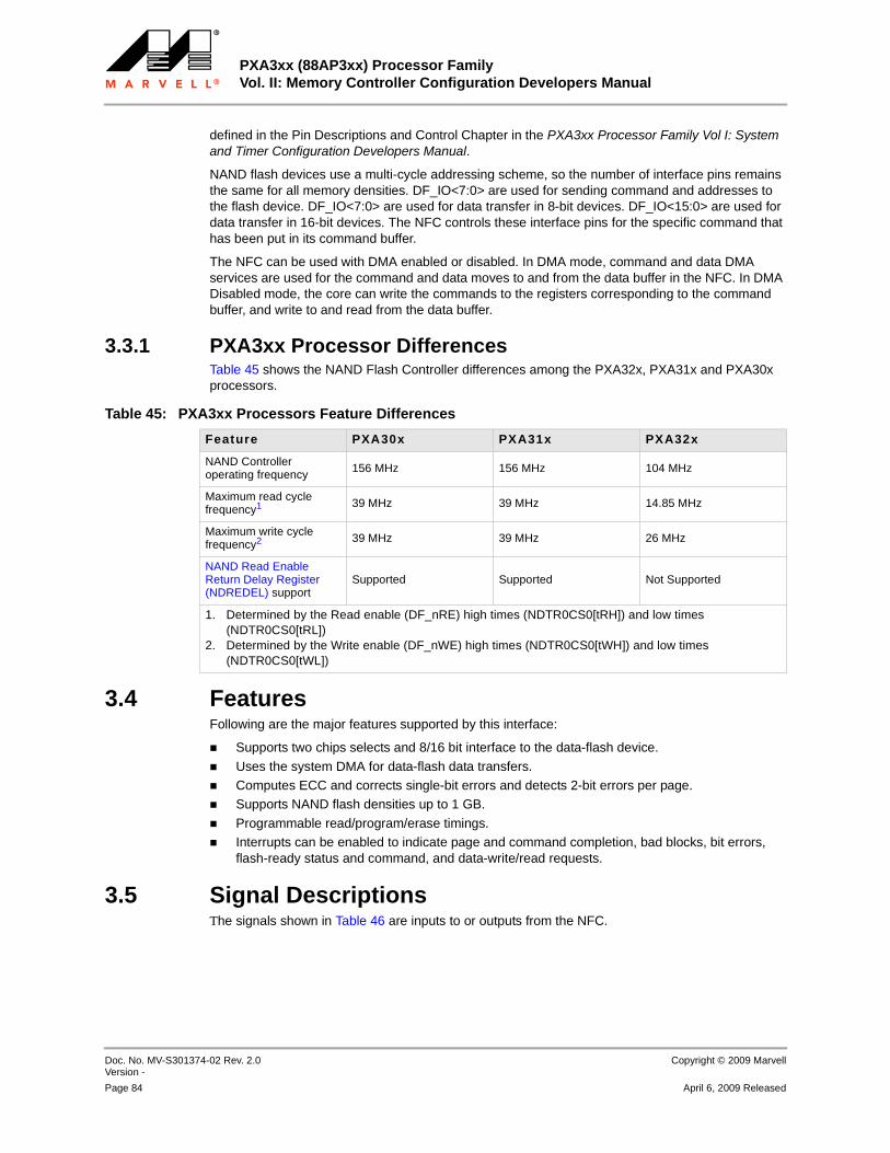
PXA3xx (88AP3xx) Processor Family Vol. II: Memory Controller Configuration Developers Manual
Doc. No. MV-S301374-02 Rev. 2.0 Version -
Copyright © 2009 Marvell
Page 84 April 6, 2009 Released
12345678910111213141516171819202122232425262728293031323334353637383940414243444546474849505152535455565758
defined in the Pin Descriptions and Control Chapter in the PXA3xx Processor Family Vol I: System and Timer Configuration Developers Manual.
NAND flash devices use a multi-cycle addressing scheme, so the number of interface pins remains the same for all memory densities. DF_IO<7:0> are used for sending command and addresses to the flash device. DF_IO<7:0> are used for data transfer in 8-bit devices. DF_IO<15:0> are used for data transfer in 16-bit devices. The NFC controls these interface pins for the specific command that has been put in its command buffer.
The NFC can be used with DMA enabled or disabled. In DMA mode, command and data DMA services are used for the command and data moves to and from the data buffer in the NFC. In DMA Disabled mode, the core can write the commands to the registers corresponding to the command buffer, and write to and read from the data buffer.
3.3.1 PXA3xx Processor DifferencesTable 45 shows the NAND Flash Controller differences among the PXA32x, PXA31x and PXA30x processors.
3.4 FeaturesFollowing are the major features supported by this interface:
Supports two chips selects and 8/16 bit interface to the data-flash device.
Uses the system DMA for data-flash data transfers.Computes ECC and corrects single-bit errors and detects 2-bit errors per page.Supports NAND flash densities up to 1 GB.
Programmable read/program/erase timings.Interrupts can be enabled to indicate page and command completion, bad blocks, bit errors, flash-ready status and command, and data-write/read requests.
3.5 Signal DescriptionsThe signals shown in Table 46 are inputs to or outputs from the NFC.
Table 45: PXA3xx Processors Feature Differences
Feature PXA30x PXA31x PXA32x
NAND Controller operating frequency 156 MHz 156 MHz 104 MHz
Maximum read cycle frequency1 39 MHz 39 MHz 14.85 MHz
Maximum write cycle frequency2 39 MHz 39 MHz 26 MHz
NAND Read Enable Return Delay Register (NDREDEL) support
Supported Supported Not Supported
1. Determined by the Read enable (DF_nRE) high times (NDTR0CS0[tRH]) and low times (NDTR0CS0[tRL])
2. Determined by the Write enable (DF_nWE) high times (NDTR0CS0[tWH]) and low times (NDTR0CS0[tWL])
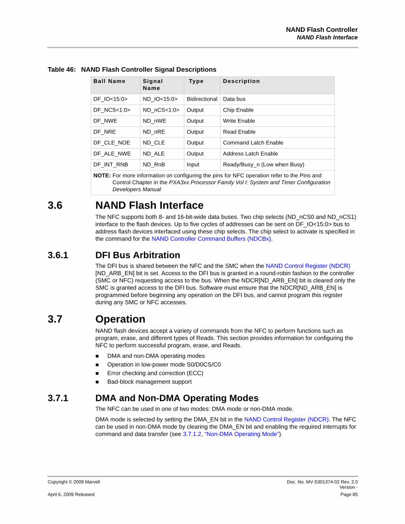
NAND Flash ControllerNAND Flash Interface
Copyright © 2009 Marvell Doc. No. MV-S301374-02 Rev. 2.0Version -
April 6, 2009 Released Page 85
12345678910111213141516171819202122232425262728293031323334353637383940414243444546474849505152535455565758
3.6 NAND Flash Interface The NFC supports both 8- and 16-bit-wide data buses. Two chip selects (ND_nCS0 and ND_nCS1) interface to the flash devices. Up to five cycles of addresses can be sent on DF_IO<15:0> bus to address flash devices interfaced using these chip selects. The chip select to activate is specified in the command for the NAND Controller Command Buffers (NDCBx).
3.6.1 DFI Bus ArbitrationThe DFI bus is shared between the NFC and the SMC when the NAND Control Register (NDCR) [ND_ARB_EN] bit is set. Access to the DFI bus is granted in a round-robin fashion to the controller (SMC or NFC) requesting access to the bus. When the NDCR[ND_ARB_EN] bit is cleared only the SMC is granted access to the DFI bus. Software must ensure that the NDCR[ND_ARB_EN] is programmed before beginning any operation on the DFI bus, and cannot program this register during any SMC or NFC accesses.
3.7 OperationNAND flash devices accept a variety of commands from the NFC to perform functions such as program, erase, and different types of Reads. This section provides information for configuring the NFC to perform successful program, erase, and Reads.
DMA and non-DMA operating modes
Operation in low-power mode S0/D0CS/C0Error checking and correction (ECC)Bad-block management support
3.7.1 DMA and Non-DMA Operating ModesThe NFC can be used in one of two modes: DMA mode or non-DMA mode.
DMA mode is selected by setting the DMA_EN bit in the NAND Control Register (NDCR). The NFC can be used in non-DMA mode by clearing the DMA_EN bit and enabling the required interrupts for command and data transfer (see 3.7.1.2, “Non-DMA Operating Mode”).
Table 46: NAND Flash Controller Signal Descriptions
Ball Name Signal Name
Type Descript ion
DF_IO<15:0> ND_IO<15:0> Bidirectional Data bus
DF_NCS<1:0> ND_nCS<1:0> Output Chip Enable
DF_NWE ND_nWE Output Write Enable
DF_NRE ND_nRE Output Read Enable
DF_CLE_NOE ND_CLE Output Command Latch Enable
DF_ALE_NWE ND_ALE Output Address Latch Enable
DF_INT_RNB ND_RnB Input Ready/Busy_n (Low when Busy)
NOTE: For more information on configuring the pins for NFC operation refer to the Pins and Control Chapter in the PXA3xx Processor Family Vol I: System and Timer Configuration Developers Manual
PXA3xx (88AP3xx) Processor Family Vol. II: Memory Controller Configuration Developers Manual
Doc. No. MV-S301374-02 Rev. 2.0 Version -
Copyright © 2009 Marvell
Page 86 April 6, 2009 Released
12345678910111213141516171819202122232425262728293031323334353637383940414243444546474849505152535455565758
Note
Note When operating in DMA mode, the core should not access command and data buffers in the NFC. Similarly, when the NFC is operating in non-DMA mode, the DMA controller should not access command and data buffers.
3.7.1.1 DMA Operating ModeIn DMA operating mode, the NFC uses the services of the system DMA controller for command and data transfers. Command DMA and data DMA services are requested for the transfer of a command to the command buffer and data to/from the data buffer.
3.7.1.1.1 Command DMA Command DMA transfers the command and address to be sent to the external NAND flash device, from the source to the NFC command buffer. The command DMA Descriptor must be programmed to transfer exactly 12 bytes of command (which contains the command for the NAND flash as well as the address and command-control information (CMD_CTRL), as defined in the format shown in Table 47, “Command Format”).
The CMD_TYPE field in CMD_CTRL defines the type of command.
The double-byte command (DBC) bit in the CMD_CTRL field indicates that the present command is a two-byte command, where CMD1 and CMD2 are the commands sent to the flash device in the CMD1-ADDR-CMD2 (or CMD1-ADDR-DATA-CMD2 in case of program commands) sequence. If the current command is a single-byte command, only CMD1 and address are sent, and the sequence would be CMD1-ADDR (or CMD1-ADDR-DATA in case of program commands). The addressing (ADDR phase) is performed in multiple cycles using the ND_IO<7:0> signals. ADDR1 through ADDR5 are the addresses sent in address cycles 1 through 5, respectively. The CMD_CTRL field contains information about the number of address cycles, single/double CMD etc. as illustrated in Table 47, “Command Format”.
One command Descriptor always corresponds to a single- or double-byte NAND flash command. It is possible to chain multiple command descriptors, so that the NFC executes them sequentially. A command-DMA request is triggered only when one of the following conditions is met.ND_RUN bit is set in the NAND Control Register (NDCR) to fetch the first command, and the command buffer is empty.Ready/Busy_ (R/B_) input is asserted low by the addressed NAND flash device, after the transfer of any command except read ID and read status, with NC (next command) bit set in the CMD_CTRL field.The execution is completed and data buffer emptied by data DMA for read ID or read status commands with NC (next command) bit set in CMD_CTRL field.
Note
Note If any program/erase command with NC set results in a bad-block error, additional command DMA requests are not sent. Software must reprogram the Descriptor chain in such an instance.
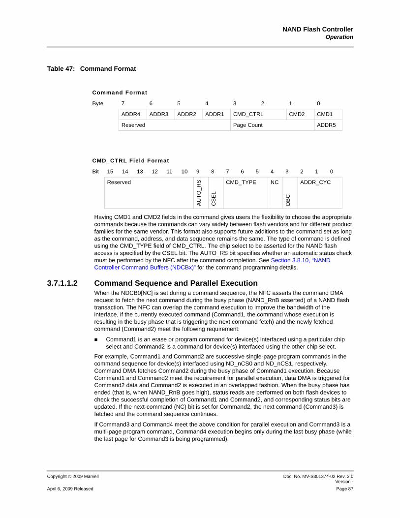
NAND Flash ControllerOperation
Copyright © 2009 Marvell Doc. No. MV-S301374-02 Rev. 2.0Version -
April 6, 2009 Released Page 87
12345678910111213141516171819202122232425262728293031323334353637383940414243444546474849505152535455565758
Having CMD1 and CMD2 fields in the command gives users the flexibility to choose the appropriate commands because the commands can vary widely between flash vendors and for different product families for the same vendor. This format also supports future additions to the command set as long as the command, address, and data sequence remains the same. The type of command is defined using the CMD_TYPE field of CMD_CTRL. The chip select to be asserted for the NAND flash access is specified by the CSEL bit. The AUTO_RS bit specifies whether an automatic status check must be performed by the NFC after the command completion. See Section 3.8.10, “NAND Controller Command Buffers (NDCBx)” for the command programming details.
3.7.1.1.2 Command Sequence and Parallel ExecutionWhen the NDCB0[NC] is set during a command sequence, the NFC asserts the command DMA request to fetch the next command during the busy phase (NAND_RnB asserted) of a NAND flash transaction. The NFC can overlap the command execution to improve the bandwidth of the interface, if the currently executed command (Command1, the command whose execution is resulting in the busy phase that is triggering the next command fetch) and the newly fetched command (Command2) meet the following requirement:
Command1 is an erase or program command for device(s) interfaced using a particular chip select and Command2 is a command for device(s) interfaced using the other chip select.
For example, Command1 and Command2 are successive single-page program commands in the command sequence for device(s) interfaced using ND_nCS0 and ND_nCS1, respectively. Command DMA fetches Command2 during the busy phase of Command1 execution. Because Command1 and Command2 meet the requirement for parallel execution, data DMA is triggered for Command2 data and Command2 is executed in an overlapped fashion. When the busy phase has ended (that is, when NAND_RnB goes high), status reads are performed on both flash devices to check the successful completion of Command1 and Command2, and corresponding status bits are updated. If the next-command (NC) bit is set for Command2, the next command (Command3) is fetched and the command sequence continues.
If Command3 and Command4 meet the above condition for parallel execution and Command3 is a multi-page program command, Command4 execution begins only during the last busy phase (while the last page for Command3 is being programmed).
Table 47: Command Format
Command Format
Byte 7 6 5 4 3 2 1 0
ADDR4 ADDR3 ADDR2 ADDR1 CMD_CTRL CMD2 CMD1
Reserved Page Count ADDR5
CMD_CTRL Field Format
Bit 15 14 13 12 11 10 9 8 7 6 5 4 3 2 1 0
Reserved
AU
TO
_RS
CS
EL
CMD_TYPE NC
DB
C
ADDR_CYC

PXA3xx (88AP3xx) Processor Family Vol. II: Memory Controller Configuration Developers Manual
Doc. No. MV-S301374-02 Rev. 2.0 Version -
Copyright © 2009 Marvell
Page 88 April 6, 2009 Released
12345678910111213141516171819202122232425262728293031323334353637383940414243444546474849505152535455565758
When ND_nCS0 and ND_nCS1 are used to interface to NAND flash devices, faster operation can be achieved by programming the devices in an interleaved fashion (alternating between ND_nCS0 and ND_nCS1), rather than programming them sequentially.
Note
Note NAND_RnB is intended to remain low and only rise once when two commands are overlapped. Follow these steps if it is necessary to know when the flash device has truly completed the transaction in addition to when it has been issued by the NFC:
1. Wait for Command Done signal (NAND Controller Status Register (NDSR)[CSx_CMDD] to be set.2. Wait amount of time (program time or erase time) specified by the device spec.3. Issue manual status read to check Ready status. If Ready is set this signifies the operation is complete.
If the commands do not meet the requirement for parallel execution, they are executed sequentially.
Command1, Command2, Command3 and Command4 are commands programmed into the NAND Controller Command Buffers (NDCBx).
3.7.1.1.3 Data DMAA NAND flash page consists of a main memory area and spare area. The main memory area is where data is stored, and spare area is used to store ECC and file-system-dependent information. Data DMA is used to write to and read from main memory and the spare areas of one or more pages. The same data buffer and DMA request is used for both Read and Write transactions because only one of the two transactions is ongoing at any given time.
If the command transferred to the command buffer is a Write, data DMA is used to fill up the data buffer. The number of data bytes that can be written per page could vary, depending on the use of the spare area of the NAND flash (see Section 3.7.6.2, “Data Area Available Under NDCR[PAGE_SZ] Settings”). The total number of bytes transferred to the data buffer for a page program must be a multiple of 32 bytes. For example, if the page size is 512 bytes and spare area is 16 bytes, the available space per page is 520 bytes if ECC is enabled, (512 bytes of main memory and 8 bytes of spare area). The data DMA should transfer 24 bytes of dummy data so that 544 bytes get transferred to the data buffer for a single-page program because 544 is the closest number that is greater than 520 and is a multiple of 32.
The 24 bytes of dummy data are not written to the flash. The dummy data bytes are added so that a single data Descriptor could service multiple pages. For a multi-page program command, set up the data-DMA Descriptor(s) to transfer a multiple of 544 bytes in the above-mentioned case. Set up the Write-data DMA Descriptor(s) to transfer the required number of bytes with the NFC data buffer as the target location. Multiple-Write data Descriptors can be chained to accomplish the data transfer corresponding to a single command. Partial-page programming is not supported by the NFC.
If command and data DMA Descriptor(s) are configured for a multiple-page program, the NFC data buffer fills with a page of data. After the data buffer is emptied by the completion of a page program, data DMA resumes loading the next page data in the data buffer. This sequence continues until the specified number of pages in the command are transferred to the flash device, or a bad block is encountered.
When a Read command is transferred to the NFC command buffer, the Read command is issued to the flash memory. The number of bytes DMA requires per page is a multiple of 32 bytes. The NFC stuffs zeroes as dummy bytes at the end of the spare-area data so that the data read by DMA per

NAND Flash ControllerOperation
Copyright © 2009 Marvell Doc. No. MV-S301374-02 Rev. 2.0Version -
April 6, 2009 Released Page 89
12345678910111213141516171819202122232425262728293031323334353637383940414243444546474849505152535455565758
page is a multiple of 32 bytes. The application ignores the added zeros read from the flash controller data buffer. Partial page reads are not supported by the NFC.
If a multiple-page read is attempted in a single command, the operation proceeds in a page-by-page manner; that is, after reading a page of data, the NFC waits until the data buffer is emptied by data (read) DMA, before reading the next page data from flash. For a Read status and Read ID commands, set up data DMA to transfer 8 bytes of data.
For more information on DMA transfers refer to the DMA chapter in the PXA3xx Processor Family Vol I: System and Timer Configuration Developers Manual.
Note
Note A data DMA request is not asserted for erase and reset commands
3.7.1.1.4 Data DMA RequirementsThe following list summarizes the programing model for data DMA. Each set of data DMA Descriptors for a command should meet these requirements.
The burst length (size) for the data DMA must be programmed as 32 bytes.For Write commands, the NFC data buffer (NDDB) must be the target of the data DMA and for Read commands; NDDB must be the source.The number of bytes of data written to a page must be a multiple of 32 bytes. Software must pad enough dummy data to make the data length a multiple of 32 bytes. Refer to Section 3.7.6.2, “Data Area Available Under NDCR[PAGE_SZ] Settings” for the number of bytes of data that must be transferred per page by Write-data DMA.
For Read commands (except status Read and Read ID), the number of bytes of data expected per page must be a multiple of 32 bytes, because the NFC always stuffs zeroes at the end of spare data to make the number of bytes per page a multiple of 32 bytes. Refer to Section 3.7.6.2 for the number of bytes of data that must be transferred per page by Read-data DMA.
For Read-ID and Read-status commands, the data-DMA Descriptor must be set up to transfer 8 bytes because the NFC allocates one buffer entry (8 bytes) to hold the Read data for these commands. Valid data is aligned to the LSB and users must discard non-valid bytes, for example, for a 5-byte read-ID command, bytes 0 through 4 are valid while bytes 5 through 7 should be discarded.
3.7.1.2 Non-DMA Operating ModeIn non-DMA operating mode, the following interrupts must be enabled by clearing the appropriate mask bits in the NAND Control Register (NDCR).
Write-Data Request interruptRead-Data Request interruptWrite-Command Request interrupt
In this mode, the NDCR[ND_RUN] bit must be set after configuring the NFC registers, and the core responds to a Write-command request interrupt by writing the command to the command buffer (NDCBx). NDCBx should be written only after receiving a Write-command request. If the command is a Write (single page or multi-page), the Write-data request interrupt is activated, and the core Writes data corresponding to a page to the NAND Controller Data Buffer (NDDB). For multi-page Writes, the Write-data request interrupt gets activated multiple times, requesting the core for a page of data each time. Similarly for Read operations, the Read-data request interrupt is activated after reading a page of data from the flash device, and the PXA30x processor or PXA31x processor responds to this interrupt by emptying the data buffer.
PXA3xx (88AP3xx) Processor Family Vol. II: Memory Controller Configuration Developers Manual
Doc. No. MV-S301374-02 Rev. 2.0 Version -
Copyright © 2009 Marvell
Page 90 April 6, 2009 Released
12345678910111213141516171819202122232425262728293031323334353637383940414243444546474849505152535455565758
For Read ID and Read status commands, the core reads 8 bytes from NDDB, because the NFC allocates one buffer entry (8 bytes) to hold the read data for these commands. Valid data is aligned to the LSB; discard non-valid bytes, for example, for a 5-byte read-ID command, bytes 0 through 4 are valid while bytes 5 through 7 should be discarded.
Note
Note Even if interrupts are not enabled, software can poll the NAND Controller Status Register (NDSR) bits corresponding to the above-mentioned interrupts to perform Write/Read data and Write commands in non-DMA Operating mode.
• If writing/reading to/from the NDDB from the ISR, clear the WRDREQ/RDDREQ status bits by writing to NDSR before accessing the NDDB. This action prevents missing WRDREQ/RDDREQ interrupts for subsequent pages during multi-page PROGRAM and multi-page Read cycles.
• If issuing a command with the next-command (NC) bit set, the next command should not be Read ID or Read status because of difficulties with servicing interrupts. Read ID and Read status commands are too short for the interrupt service routine to finish servicing the first Command Done interrupt in time to acknowledge the second Command Done interrupt and therefore it goes undetected.
3.7.2 Low-Power Mode OperationThe NFC operates only during normal run (S0/D0/C0 and S0/D0/C1) mode and in S0/D0CS/C0 mode.
Note
Note In S0/D0CS/C0 mode the NAND controller clock frequency varies between 25.5 MHz and 34.5 MHz. Since all the timing parameters are relative to NAND clock period, highest frequency (34.5 MHz) should be assumed when setting up the NDTR0CS0 and NDTR1CS0 registers, but expect performance at the lowest frequency (25.5 MHz).
In S0/D1/C2 and S0/D2/C2 mode of operation, the NFC is not operational and must be idled before entering the mode. In particular, all data must be removed from the buffers, and the end of a command (a full block Read, program, or erase) must be reached. If the mode is entered while the unit is not idle or partway through a block, then that block must be repeated. The cycle on the external bus (the Read or Write cycle) currently underway is correctly finished; however, the sets of Reads and Writes (the multiple address cycles) are not finished.
The recommended sequence for going into a lower power mode (S0/D1/C2 or S0/D2/C2) is to first clear the ND_RUN bit and then to examine the registers to determine what position has been reached in a sequence of commands. The last command should then be configured to be restarted once the low-power state is exited.
Once low-power mode is exited, then the ND_RUN bit should be reset.
In D3, there is no retained state. On entry, the current bus cycle is finished, but then the command queue is cleared, and any command in progress is not completed.
If low-power mode is entered once a block has been sent to the NAND AND the programming command is given (or during an erase), the program or erase is completed but no status checking is performed. In this case, the operation must be repeated.
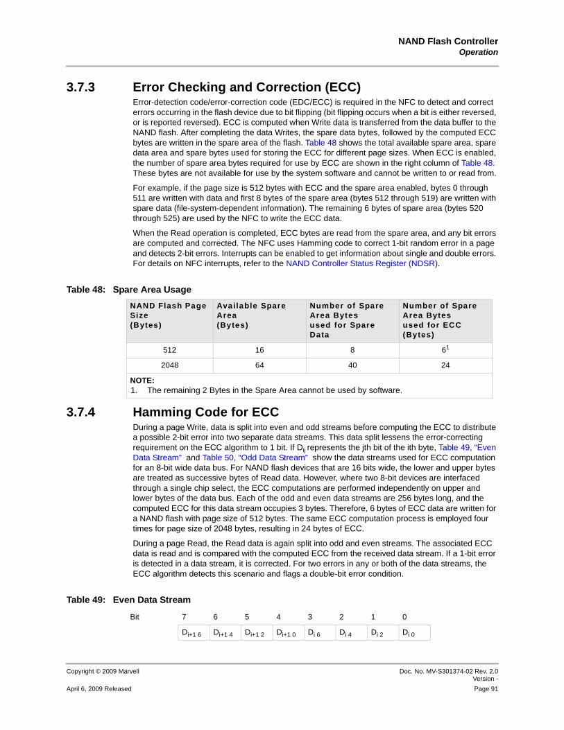
NAND Flash ControllerOperation
Copyright © 2009 Marvell Doc. No. MV-S301374-02 Rev. 2.0Version -
April 6, 2009 Released Page 91
12345678910111213141516171819202122232425262728293031323334353637383940414243444546474849505152535455565758
3.7.3 Error Checking and Correction (ECC)Error-detection code/error-correction code (EDC/ECC) is required in the NFC to detect and correct errors occurring in the flash device due to bit flipping (bit flipping occurs when a bit is either reversed, or is reported reversed). ECC is computed when Write data is transferred from the data buffer to the NAND flash. After completing the data Writes, the spare data bytes, followed by the computed ECC bytes are written in the spare area of the flash. Table 48 shows the total available spare area, spare data area and spare bytes used for storing the ECC for different page sizes. When ECC is enabled, the number of spare area bytes required for use by ECC are shown in the right column of Table 48. These bytes are not available for use by the system software and cannot be written to or read from.
For example, if the page size is 512 bytes with ECC and the spare area enabled, bytes 0 through 511 are written with data and first 8 bytes of the spare area (bytes 512 through 519) are written with spare data (file-system-dependent information). The remaining 6 bytes of spare area (bytes 520 through 525) are used by the NFC to write the ECC data.
When the Read operation is completed, ECC bytes are read from the spare area, and any bit errors are computed and corrected. The NFC uses Hamming code to correct 1-bit random error in a page and detects 2-bit errors. Interrupts can be enabled to get information about single and double errors. For details on NFC interrupts, refer to the NAND Controller Status Register (NDSR).
3.7.4 Hamming Code for ECCDuring a page Write, data is split into even and odd streams before computing the ECC to distribute a possible 2-bit error into two separate data streams. This data split lessens the error-correcting requirement on the ECC algorithm to 1 bit. If Dij represents the jth bit of the ith byte, Table 49, “Even Data Stream” and Table 50, “Odd Data Stream” show the data streams used for ECC computation for an 8-bit wide data bus. For NAND flash devices that are 16 bits wide, the lower and upper bytes are treated as successive bytes of Read data. However, where two 8-bit devices are interfaced through a single chip select, the ECC computations are performed independently on upper and lower bytes of the data bus. Each of the odd and even data streams are 256 bytes long, and the computed ECC for this data stream occupies 3 bytes. Therefore, 6 bytes of ECC data are written for a NAND flash with page size of 512 bytes. The same ECC computation process is employed four times for page size of 2048 bytes, resulting in 24 bytes of ECC.
During a page Read, the Read data is again split into odd and even streams. The associated ECC data is read and is compared with the computed ECC from the received data stream. If a 1-bit error is detected in a data stream, it is corrected. For two errors in any or both of the data streams, the ECC algorithm detects this scenario and flags a double-bit error condition.
Table 48: Spare Area Usage
NAND Flash Page Size(Bytes)
Available Spare Area (Bytes)
Number of Spare Area Bytesused for Spare Data
Number of Spare Area Bytesused for ECC (Bytes)
512 16 8 61
2048 64 40 24
NOTE:1. The remaining 2 Bytes in the Spare Area cannot be used by software.
Table 49: Even Data Stream
Bit 7 6 5 4 3 2 1 0
Di+1 6 Di+1 4 Di+1 2 Di+1 0 Di 6 Di 4 Di 2 Di 0

PXA3xx (88AP3xx) Processor Family Vol. II: Memory Controller Configuration Developers Manual
Doc. No. MV-S301374-02 Rev. 2.0 Version -
Copyright © 2009 Marvell
Page 92 April 6, 2009 Released
12345678910111213141516171819202122232425262728293031323334353637383940414243444546474849505152535455565758
3.7.5 Bad Block Management SupportThe NFC performs a status check after each program/erase operation to determine if the transaction was successful. This status check can be disabled by clearing the AUTO_RS bit in the command buffer. (See Table 65, “NDCB0 Bit Definitions” ). If a status check returns an error, as indicated by a 1 in the LSB of the status-Read data, a Bad-Block-Detect interrupt (if enabled) is sent out and Bad Block registers (See Table 61, “NDBBRx Bit Definitions” ) can be read to determine the address of the bad block.
3.7.6 Command Execution When Bad Blocks are DetectedWhen a bad block is detected, the behavior of the NFC remains the same, regardless of whether commands are executed sequentially or in parallel. The command without a bad-block detection is completed, but the command that resulted in a bad-block detection is considered as “not executed.” (If it is a program command, it must be executed again after the command Descriptors have been reprogrammed to handle the bad-block scenario.) However, no new command is fetched by command DMA even if the NC bit is set for the last command, since a bad- block scenario is encountered. As a result of a bad-block detection, the NDCR[ND_RUN] bit is cleared after the command buffer is emptied. Resume the operation by setting ND_RUN after command-Descriptor modifications.
Table 50: Odd Data Stream
Bit 7 6 5 4 3 2 1 0
Di+1 7 Di+1 5 Di+1 3 Di+1 1 Di 7 Di 5 Di 3 Di 1
Figure 8: Error Detection Process
X O R r e s u l t s i n a l l b i t s e q u a l t o
z e r o
N o e r r o r E r r o r d e t e c t e d
N o
Y e s
O r ig in a l E C C c o d e X O R e d w i t h n e w g e n e r a t e d E C C c o d e
G e n e r a t e E C C c o d e d u r in g p r o g r a m o p e r a t i o n
G e n e r a t e N e w E C C c o d e d u r in g d a t a r e a d
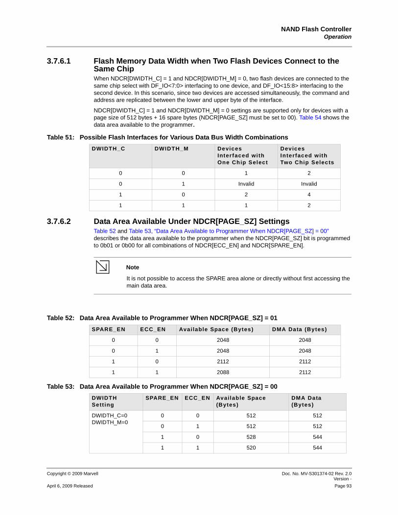
NAND Flash ControllerOperation
Copyright © 2009 Marvell Doc. No. MV-S301374-02 Rev. 2.0Version -
April 6, 2009 Released Page 93
12345678910111213141516171819202122232425262728293031323334353637383940414243444546474849505152535455565758
3.7.6.1 Flash Memory Data Width when Two Flash Devices Connect to the Same ChipWhen NDCR[DWIDTH_C] = 1 and NDCR[DWIDTH_M] = 0, two flash devices are connected to the same chip select with DF_IO<7:0> interfacing to one device, and DF_IO<15:8> interfacing to the second device. In this scenario, since two devices are accessed simultaneously, the command and address are replicated between the lower and upper byte of the interface.
NDCR[DWIDTH_C] = 1 and NDCR[DWIDTH_M] = 0 settings are supported only for devices with a page size of 512 bytes + 16 spare bytes (NDCR[PAGE_SZ] must be set to 00). Table 54 shows the data area available to the programmer.
3.7.6.2 Data Area Available Under NDCR[PAGE_SZ] SettingsTable 52 and Table 53, “Data Area Available to Programmer When NDCR[PAGE_SZ] = 00” describes the data area available to the programmer when the NDCR[PAGE_SZ] bit is programmed to 0b01 or 0b00 for all combinations of NDCR[ECC_EN] and NDCR[SPARE_EN].
Note
Note It is not possible to access the SPARE area alone or directly without first accessing the main data area.
Table 51: Possible Flash Interfaces for Various Data Bus Width Combinations
DWIDTH_C DWIDTH_M Devices Interfaced with One Chip Select
Devices Interfaced with Two Chip Selects
0 0 1 2
0 1 Invalid Invalid
1 0 2 4
1 1 1 2
Table 52: Data Area Available to Programmer When NDCR[PAGE_SZ] = 01
SPARE_EN ECC_EN Available Space (Bytes) DMA Data (Bytes)
0 0 2048 2048
0 1 2048 2048
1 0 2112 2112
1 1 2088 2112
Table 53: Data Area Available to Programmer When NDCR[PAGE_SZ] = 00
DWIDTH Sett ing
SPARE_EN ECC_EN Available Space (Bytes)
DMA Data (Bytes)
DWIDTH_C=0DWIDTH_M=0
0 0 512 512
0 1 512 512
1 0 528 544
1 1 520 544
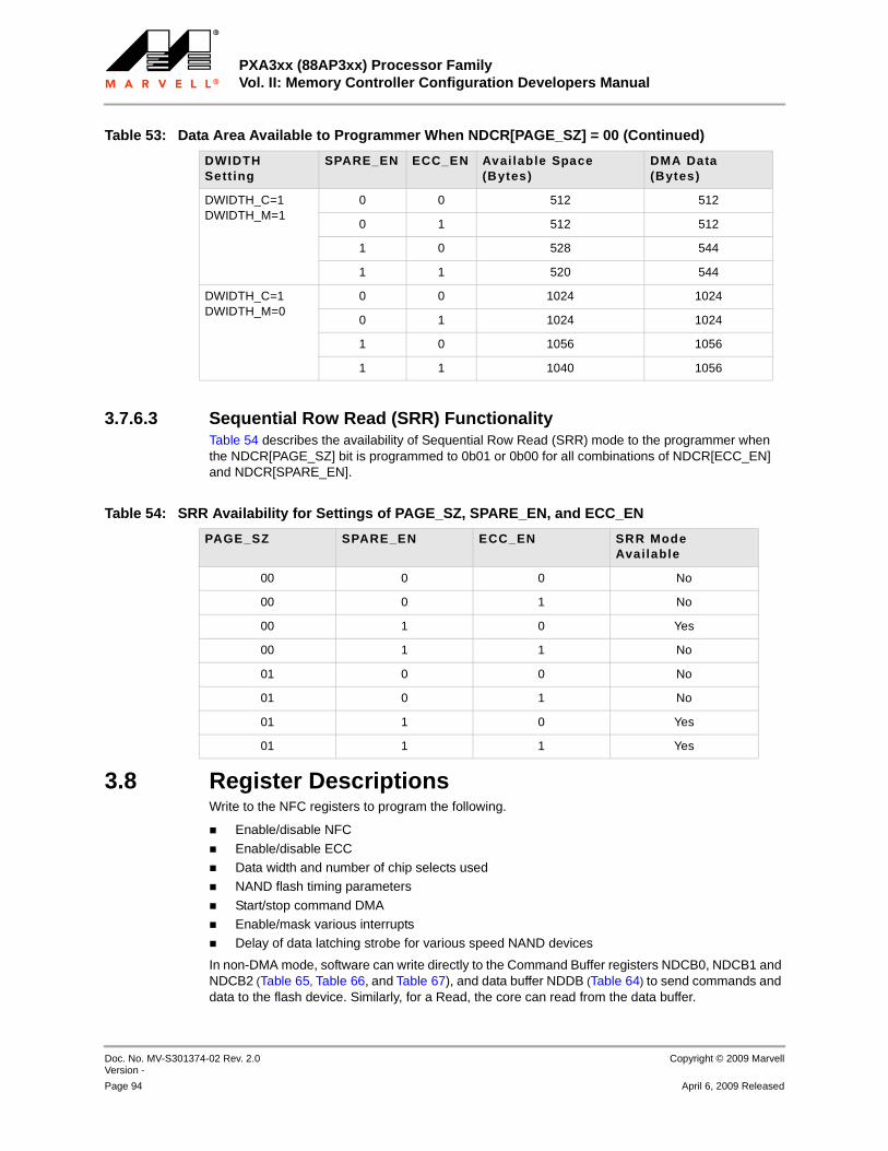
PXA3xx (88AP3xx) Processor Family Vol. II: Memory Controller Configuration Developers Manual
Doc. No. MV-S301374-02 Rev. 2.0 Version -
Copyright © 2009 Marvell
Page 94 April 6, 2009 Released
12345678910111213141516171819202122232425262728293031323334353637383940414243444546474849505152535455565758
3.7.6.3 Sequential Row Read (SRR) FunctionalityTable 54 describes the availability of Sequential Row Read (SRR) mode to the programmer when the NDCR[PAGE_SZ] bit is programmed to 0b01 or 0b00 for all combinations of NDCR[ECC_EN] and NDCR[SPARE_EN].
3.8 Register DescriptionsWrite to the NFC registers to program the following.
Enable/disable NFC
Enable/disable ECCData width and number of chip selects usedNAND flash timing parameters
Start/stop command DMAEnable/mask various interruptsDelay of data latching strobe for various speed NAND devices
In non-DMA mode, software can write directly to the Command Buffer registers NDCB0, NDCB1 and NDCB2 (Table 65, Table 66, and Table 67), and data buffer NDDB (Table 64) to send commands and data to the flash device. Similarly, for a Read, the core can read from the data buffer.
DWIDTH_C=1DWIDTH_M=1
0 0 512 512
0 1 512 512
1 0 528 544
1 1 520 544
DWIDTH_C=1DWIDTH_M=0
0 0 1024 1024
0 1 1024 1024
1 0 1056 1056
1 1 1040 1056
Table 53: Data Area Available to Programmer When NDCR[PAGE_SZ] = 00 (Continued)
DWIDTH Sett ing
SPARE_EN ECC_EN Available Space (Bytes)
DMA Data (Bytes)
Table 54: SRR Availability for Settings of PAGE_SZ, SPARE_EN, and ECC_EN
PAGE_SZ SPARE_EN ECC_EN SRR Mode Available
00 0 0 No
00 0 1 No
00 1 0 Yes
00 1 1 No
01 0 0 No
01 0 1 No
01 1 0 Yes
01 1 1 Yes

NAND Flash ControllerRegister Descriptions
Copyright © 2009 Marvell Doc. No. MV-S301374-02 Rev. 2.0Version -
April 6, 2009 Released Page 95
12345678910111213141516171819202122232425262728293031323334353637383940414243444546474849505152535455565758
The Status registers contain bits that signal the error status of ECC, flash ready, bad-block detected, end-of-command execution, finish-of-page and read/write requests for the data buffer, and write request for the command buffer. Each of these hardware-detected events can signal an interrupt request to the interrupt controller.
3.8.1 Register Summary
3.8.2 NAND Control Register (NDCR)Table 56 shows the location of all bit fields in NAND Flash Control register (NDCR). Program the Timing Parameter registers (NDTR0CS0 and NDTR1CS0) and Control registers before writing to this register.
This is a read/write register. Ignore reads from reserved bits. Write 0b0 to reserved bits.
Table 55: NAND Flash Controller Register Summary
Address Name Page
0x4310_0000 NAND Control Register (NDCR) page 95
0x4310_0004 NAND Interface Timing Parameter 0 Register (NDTR0CS0) page 103
0x4310_0008 Reserved —
0x4310_000C NAND Interface Timing Parameter 1 Register (NDTR1CS0) page 105
0x4310_0010 Reserved —
0x4310_0014 NAND Controller Status Register (NDSR) page 106
0x4310_0018 NAND Controller Page Count Register (NDPCR) page 112
0x4310_001C NAND Controller Bad Block Registers (NDBBRx) (NDBBDR0) page 113
0x4310_0020 NAND Controller Bad Block Registers (NDBBRx) (NDBBDR1) page 113
0x4310_0024 NAND Read Enable Return Delay Register (NDREDEL) (PXA30x and PXA31x Processors Only)
page 114
0x4310_0028– 0x4310_003C
Reserved —
0x4310_0040 NAND Controller Data Buffer (NDDB) page 116
0x4310_0044 Reserved —
0x4310_0048 NAND Controller Command Buffers (NDCBx) (NDCB0) page 116
0x4310_004C NAND Controller Command Buffers (NDCBx) (NDCB1) page 119
0x4310_0050 NAND Controller Command Buffers (NDCBx) (NDCB2) page 120
0x4310_0054–0x4310_007C
Reserved —

PXA3xx (88AP3xx) Processor Family Vol. II: Memory Controller Configuration Developers Manual
Doc. No. MV-S301374-02 Rev. 2.0 Version -
Copyright © 2009 Marvell
Page 96 April 6, 2009 Released
12345678910111213141516171819202122232425262728293031323334353637383940414243444546474849505152535455565758
Table 56: NDCR Bit Definitions
Physical Address0x4310_0000
NDCR NAND Flash Controller
User Settings
Bit 31 30 29 28 27 26 25 24 23 22 21 20 19 18 17 16 15 14 13 12 11 10 9 8 7 6 5 4 3 2 1 0
SP
AR
E_
EN
EC
C_
EN
DM
A_
EN
ND
_R
UN
DW
IDT
H_
C
DW
IDT
H_
M
PA
GE
_S
Z
NC
SX
Re
se
rve
d
CL
R_
PG
_C
NT
Re
se
rve
d
RD
_ID
_C
NT
RA
_S
TA
RT
PG
_P
ER
_B
LK
Re
se
rve
d
ND
_A
RB
_E
N
RD
YM
CS
0_
PA
GE
DM
CS
1_
PA
GE
DM
CS
0_
CM
DD
M
CS
1_
CM
DD
M
CS
0_
BB
DM
CS
1_
BB
DM
DB
ER
RM
SB
ER
RM
WR
DR
EQ
M
RD
DR
EQ
M
WR
CM
DR
EQ
M
Reset 0 0 0 0 0 0 0 0 0 0 0 0 0 0 1 0 0 0 ? 0 1 1 1 1 1 1 1 1 1 1 1 1
Bits Access Name Descript ion
31 R/W SPARE_EN Spare Area EnableSet the spare-area enable (SPARE_EN) bit to use the spare area of the NAND flash for data storage. NOTE: If the SPARE_EN bit is set and ECC is not enabled (ECC_EN
cleared), it is possible to write to and read from the entire data area and spare area. If SPARE_EN and ECC_EN are set, the remaining spare bytes after ECC is written are available to software. Table 52 and Table 53 specify the data bytes available for program/read, to the software per page for different SPARE_EN and ECC_EN settings.
0 = Write/Read to available spare area disabled1 = Write/Read to available spare area enabled
NOTE: The number specified in the DMA data column in these tables is the number of bytes that the DMA descriptors must be configured to transfer per page when the NFC is operating in DMA mode.
NOTE: If SPARE_EN is clear, the spare area is not available to software
30 R/W ECC_EN ECC EnableWhen the ECC enable (ECC_EN) bit is set, it enables the computation of ECC and error detection and correction. When ECC_EN bit is clear, ECC computation and error checks are not performed.0 = ECC is disabled for write and read data.1 = ECC is enabled for write and read data.
29 R/W DMA_EN DMA Request EnableSet the DMA request-enable (DMA_EN) bit to enable command and data DMA requests. When this bit is clear, no DMA requests are asserted.0 = Data and Command DMA are disabled.1 = Data and Command DMA are enabled.

NAND Flash ControllerRegister Descriptions
Copyright © 2009 Marvell Doc. No. MV-S301374-02 Rev. 2.0Version -
April 6, 2009 Released Page 97
12345678910111213141516171819202122232425262728293031323334353637383940414243444546474849505152535455565758
28 R/W ND_RUN NAND Controller Run Mode When the NAND-controller run mode (ND_RUN) bit is set, the NAND controller starts to execute the command in the command buffer. If the command buffer is empty when the ND_RUN bit is set, the NAND controller asserts the command-DMA request if the DMA request is enabled. The ND_RUN bit is cleared when the NAND flash controller finishes the execution of a command with the next command (NC) bit clear, indicating the end of the command sequence. For a bad-block detect, ND_RUN is cleared after the command buffer is emptied. Clearing the ND_RUN bit during a command execution results in an immediate termination of transactions to the flash device and clears the data and command buffers.0 = NAND controller is not in run mode.1 = NAND controller is in run mode.
27 R/W DWIDTH_C Data Bus Width of the NFCDefines the data-bus width used by the NFC to communicate to the NAND flash device(s). Table 51 shows the valid data-width settings.0 = Data Bus width is 8 bits1 = Data Bus width is 16 bits
26 R/W DWIDTH_M Data Bus Width of the NAND Flash MemoryDefines the data bus width of the NAND flash-memory devices used in the memory system. DWIDTH_M and DWIDTH_C determine the way NAND flash devices are interfaced. Table 51 shows the valid data-width settings. 0 = Data Bus width is 8 bits1 = Data Bus width is 16 bits
25:24 R/W PAGE_SZ Page Size of the Flash deviceDefines the page size of the NAND flash memory. All NAND devices used in the NAND flash-memory system must have the same bus width, page size, command set, and timing parameters.Table 52 and Table 53 describes the data area available to the programmer when PAGE_SZ is set to 00 and 01.0b00 - 512 bytes main memory and 16 bytes spare area0b01 - 2048 bytes main memory and 64 bytes spare area0b10 - reserved0b11 - reserved
Table 56: NDCR Bit Definitions (Continued)
Physical Address0x4310_0000
NDCR NAND Flash Controller
User Settings
Bit 31 30 29 28 27 26 25 24 23 22 21 20 19 18 17 16 15 14 13 12 11 10 9 8 7 6 5 4 3 2 1 0
SP
AR
E_
EN
EC
C_
EN
DM
A_
EN
ND
_R
UN
DW
IDT
H_
C
DW
IDT
H_
M
PA
GE
_S
Z
NC
SX
Re
se
rve
d
CL
R_
PG
_C
NT
Re
se
rve
d
RD
_ID
_C
NT
RA
_S
TA
RT
PG
_P
ER
_B
LK
Re
se
rve
d
ND
_A
RB
_E
N
RD
YM
CS
0_
PA
GE
DM
CS
1_
PA
GE
DM
CS
0_
CM
DD
M
CS
1_
CM
DD
M
CS
0_
BB
DM
CS
1_
BB
DM
DB
ER
RM
SB
ER
RM
WR
DR
EQ
M
RD
DR
EQ
M
WR
CM
DR
EQ
M
Reset 0 0 0 0 0 0 0 0 0 0 0 0 0 0 1 0 0 0 ? 0 1 1 1 1 1 1 1 1 1 1 1 1
Bits Access Name Descript ion

PXA3xx (88AP3xx) Processor Family Vol. II: Memory Controller Configuration Developers Manual
Doc. No. MV-S301374-02 Rev. 2.0 Version -
Copyright © 2009 Marvell
Page 98 April 6, 2009 Released
12345678910111213141516171819202122232425262728293031323334353637383940414243444546474849505152535455565758
23 R/W NCSX Chip Select Don’t Care BitThe nCS “don’t-care” bit (NCSX) should be set if the NAND flash device supports chip-select don’t care during the busy phase (while Ready/Busy_ is low) of a read operation, or if sequential page read is not wanted. If the NAND flash requires the chip enable to be asserted during the read busy phase (the requirement for devices supporting sequential page read), the NCSX bit should be clear. When NCSX bit is clear, all multi-page reads are completed sequentially. The device is addressed only when the first page is read, and subsequent page reads are performed by toggling ND_nRE when the device is ready. Consult the data sheet of the flash part under “Sequential Row Read” or similar for details.NOTE: Sequential Row Reads are supported only when the entire
page (including the spare area) is read by the NFC. For more information on Sequential Row Reads refer to Section 3.7.6.3
0 = Chip select should be asserted during read busy phase1 = Chip select is “don’t care” during read busy phase
22 — — reserved
21 — — reserved
20 R/W CLR_PG_CNT
Clear Page CountThe clear-page-count (CLR_PG_CNT) bit, when set, clears the Page Count register (see Table 60). After the NAND Interface Page Count register is cleared, the CLR_PG_CNT bit is reset. When a program failure occurs, CLR_PG_CNT can be used to clear the page count values after software reads the number of pages programmed correctly.0 = Page count not cleared1 = Clear page count
19 — — reserved
18:16 R/W RD_ID_CNT Read ID Byte CountThe read-ID byte-count (RD_ID_CNT) bit specifies the number of data bytes to read from the flash device when a read-ID command is issued. Valid values for RD_ID_CNT are 2,4,5,6,7. For a read ID command, the page count should be set to 1 (NDCB2[Page_Count] should be zero). Values from 2 to 7. Specifies the number of bytes of read ID data to be read from the flash device
Table 56: NDCR Bit Definitions (Continued)
Physical Address0x4310_0000
NDCR NAND Flash Controller
User Settings
Bit 31 30 29 28 27 26 25 24 23 22 21 20 19 18 17 16 15 14 13 12 11 10 9 8 7 6 5 4 3 2 1 0
SP
AR
E_
EN
EC
C_
EN
DM
A_
EN
ND
_R
UN
DW
IDT
H_
C
DW
IDT
H_
M
PA
GE
_S
Z
NC
SX
Re
se
rve
d
CL
R_
PG
_C
NT
Re
se
rve
d
RD
_ID
_C
NT
RA
_S
TA
RT
PG
_P
ER
_B
LK
Re
se
rve
d
ND
_A
RB
_E
N
RD
YM
CS
0_
PA
GE
DM
CS
1_
PA
GE
DM
CS
0_
CM
DD
M
CS
1_
CM
DD
M
CS
0_
BB
DM
CS
1_
BB
DM
DB
ER
RM
SB
ER
RM
WR
DR
EQ
M
RD
DR
EQ
M
WR
CM
DR
EQ
M
Reset 0 0 0 0 0 0 0 0 0 0 0 0 0 0 1 0 0 0 ? 0 1 1 1 1 1 1 1 1 1 1 1 1
Bits Access Name Descript ion
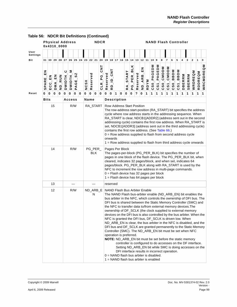
NAND Flash ControllerRegister Descriptions
Copyright © 2009 Marvell Doc. No. MV-S301374-02 Rev. 2.0Version -
April 6, 2009 Released Page 99
12345678910111213141516171819202122232425262728293031323334353637383940414243444546474849505152535455565758
15 R/W RA_START Row Address Start PositionThe row-address start-position (RA_START) bit specifies the address cycle where row address starts in the addressing sequence. When RA_START is clear, NDCB1[ADDR2] (address sent out in the second addressing cycle) contains the first row address. When RA_START is set, NDCB1[ADDR3] (address sent out in the third addressing cycle) contains the first row address. (See Table 66.)0 = Row address supplied to flash from second address cycle onwards1 = Row address supplied to flash from third address cycle onwards
14 R/W PG_PER_BLK
Pages Per BlockThe pages-per-block (PG_PER_BLK) bit specifies the number of pages in one block of the flash device. The PG_PER_BLK bit, when cleared, indicates 32 pages/block, and when set, indicates 64 pages/block. PG_PER_BLK along with RA_START is used by the NFC to increment the row address in multi-page commands.0 = Flash device has 32 pages per block1 = Flash device has 64 pages per block
13 — — reserved
12 R/W ND_ARB_EN
NAND Flash Bus Arbiter EnableThe NAND Flash bus-arbiter enable (ND_ARB_EN) bit enables the bus arbiter in the NFC, which controls the ownership of DFI bus. The DFI bus is shared between the Static Memory Controller (SMC) and the NFC to transfer data to/from external memory devices.The ownership of DF_SCLK (the clock supplied to external memory devices on the DFI bus is also controlled by the bus arbiter. When the NFC is granted the DFI bus, DF_SCLK is driven low. When ND_ARB_EN is clear, the bus arbiter in the NFC is disabled, and the DFI bus and DF_SCLK are granted permanently to the Static Memory Controller (SMC). The ND_ARB_EN bit must be set when NFC operation is preferred. NOTE: ND_ARB_EN bit must be set before the static memory
controller is configured to do accesses on the DF interface. Setting ND_ARB_EN bit while SMC is doing accesses on the DFI interface results in incorrect operation.
0 = NAND flash bus arbiter is disabled.1 = NAND flash bus arbiter is enabled
Table 56: NDCR Bit Definitions (Continued)
Physical Address0x4310_0000
NDCR NAND Flash Controller
User Settings
Bit 31 30 29 28 27 26 25 24 23 22 21 20 19 18 17 16 15 14 13 12 11 10 9 8 7 6 5 4 3 2 1 0
SP
AR
E_
EN
EC
C_
EN
DM
A_
EN
ND
_R
UN
DW
IDT
H_
C
DW
IDT
H_
M
PA
GE
_S
Z
NC
SX
Re
se
rve
d
CL
R_
PG
_C
NT
Re
se
rve
d
RD
_ID
_C
NT
RA
_S
TA
RT
PG
_P
ER
_B
LK
Re
se
rve
d
ND
_A
RB
_E
N
RD
YM
CS
0_
PA
GE
DM
CS
1_
PA
GE
DM
CS
0_
CM
DD
M
CS
1_
CM
DD
M
CS
0_
BB
DM
CS
1_
BB
DM
DB
ER
RM
SB
ER
RM
WR
DR
EQ
M
RD
DR
EQ
M
WR
CM
DR
EQ
M
Reset 0 0 0 0 0 0 0 0 0 0 0 0 0 0 1 0 0 0 ? 0 1 1 1 1 1 1 1 1 1 1 1 1
Bits Access Name Descript ion
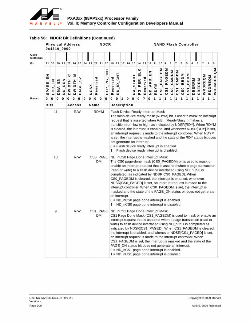
PXA3xx (88AP3xx) Processor Family Vol. II: Memory Controller Configuration Developers Manual
Doc. No. MV-S301374-02 Rev. 2.0 Version -
Copyright © 2009 Marvell
Page 100 April 6, 2009 Released
12345678910111213141516171819202122232425262728293031323334353637383940414243444546474849505152535455565758
11 R/W RDYM Flash Device Ready Interrupt MaskThe flash-device ready-mask (RDYM) bit is used to mask an interrupt request that is asserted when R/B_ (Ready/Busy_) makes a transition from low to high, as indicated by NDSR[RDY]. When RDYM is cleared, the interrupt is enabled, and whenever NDSR[RDY] is set, an interrupt request is made to the interrupt controller. When RDYM is set, the interrupt is masked and the state of the RDY status bit does not generate an interrupt.0 = Flash device ready interrupt is enabled.1 = Flash device ready interrupt is disabled.
10 R/W CS0_PAGEDM
ND_nCS0 Page Done Interrupt MaskThe CS0 page-done mask (CS0_PAGEDM) bit is used to mask or enable an interrupt request that is asserted when a page transaction (read or write) to a flash device interfaced using ND_nCS0 is completed, as indicated by NDSR[CS0_PAGED]. When CS0_PAGEDM is cleared, the interrupt is enabled; whenever NDSR[CS0_PAGED] is set, an interrupt request is made to the interrupt controller. When CS0_PAGEDM is set, the interrupt is masked and the state of the PAGE_DN status bit does not generate an interrupt.0 = ND_nCS0 page done interrupt is enabled.1 = ND_nCS0 page done interrupt is disabled.
9 R/W CS1_PAGEDM
ND_nCS1 Page Done Interrupt MaskCS1 Page Done Mask (CS1_PAGEDM) is used to mask or enable an interrupt request that is asserted when a page transaction (read or write) to flash device interfaced using ND_nCS1 is completed as indicated by NDSR[CS1_PAGED]. When CS1_PAGEDM is cleared, the interrupt is enabled, and whenever NDSR[CS1_PAGED] is set, an interrupt request is made to the interrupt controller. When CS1_PAGEDM is set, the interrupt is masked and the state of the PAGE_DN status bit does not generate an interrupt.0 = ND_nCS1 page done interrupt is enabled.1 = ND_nCS1 page done interrupt is disabled.
Table 56: NDCR Bit Definitions (Continued)
Physical Address0x4310_0000
NDCR NAND Flash Controller
User Settings
Bit 31 30 29 28 27 26 25 24 23 22 21 20 19 18 17 16 15 14 13 12 11 10 9 8 7 6 5 4 3 2 1 0
SP
AR
E_
EN
EC
C_
EN
DM
A_
EN
ND
_R
UN
DW
IDT
H_
C
DW
IDT
H_
M
PA
GE
_S
Z
NC
SX
Re
se
rve
d
CL
R_
PG
_C
NT
Re
se
rve
d
RD
_ID
_C
NT
RA
_S
TA
RT
PG
_P
ER
_B
LK
Re
se
rve
d
ND
_A
RB
_E
N
RD
YM
CS
0_
PA
GE
DM
CS
1_
PA
GE
DM
CS
0_
CM
DD
M
CS
1_
CM
DD
M
CS
0_
BB
DM
CS
1_
BB
DM
DB
ER
RM
SB
ER
RM
WR
DR
EQ
M
RD
DR
EQ
M
WR
CM
DR
EQ
M
Reset 0 0 0 0 0 0 0 0 0 0 0 0 0 0 1 0 0 0 ? 0 1 1 1 1 1 1 1 1 1 1 1 1
Bits Access Name Descript ion
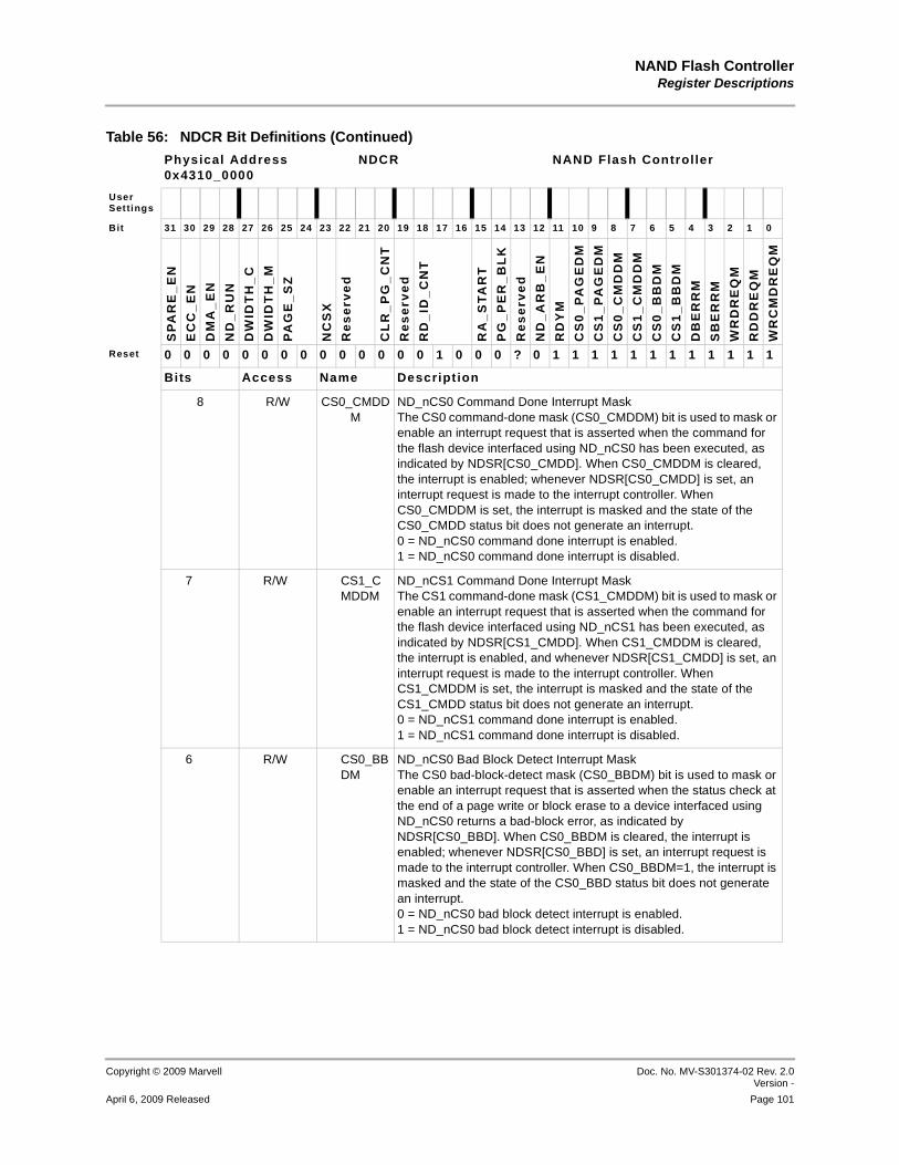
NAND Flash ControllerRegister Descriptions
Copyright © 2009 Marvell Doc. No. MV-S301374-02 Rev. 2.0Version -
April 6, 2009 Released Page 101
12345678910111213141516171819202122232425262728293031323334353637383940414243444546474849505152535455565758
8 R/W CS0_CMDDM
ND_nCS0 Command Done Interrupt MaskThe CS0 command-done mask (CS0_CMDDM) bit is used to mask or enable an interrupt request that is asserted when the command for the flash device interfaced using ND_nCS0 has been executed, as indicated by NDSR[CS0_CMDD]. When CS0_CMDDM is cleared, the interrupt is enabled; whenever NDSR[CS0_CMDD] is set, an interrupt request is made to the interrupt controller. When CS0_CMDDM is set, the interrupt is masked and the state of the CS0_CMDD status bit does not generate an interrupt.0 = ND_nCS0 command done interrupt is enabled.1 = ND_nCS0 command done interrupt is disabled.
7 R/W CS1_CMDDM
ND_nCS1 Command Done Interrupt MaskThe CS1 command-done mask (CS1_CMDDM) bit is used to mask or enable an interrupt request that is asserted when the command for the flash device interfaced using ND_nCS1 has been executed, as indicated by NDSR[CS1_CMDD]. When CS1_CMDDM is cleared, the interrupt is enabled, and whenever NDSR[CS1_CMDD] is set, an interrupt request is made to the interrupt controller. When CS1_CMDDM is set, the interrupt is masked and the state of the CS1_CMDD status bit does not generate an interrupt.0 = ND_nCS1 command done interrupt is enabled.1 = ND_nCS1 command done interrupt is disabled.
6 R/W CS0_BBDM
ND_nCS0 Bad Block Detect Interrupt MaskThe CS0 bad-block-detect mask (CS0_BBDM) bit is used to mask or enable an interrupt request that is asserted when the status check at the end of a page write or block erase to a device interfaced using ND_nCS0 returns a bad-block error, as indicated by NDSR[CS0_BBD]. When CS0_BBDM is cleared, the interrupt is enabled; whenever NDSR[CS0_BBD] is set, an interrupt request is made to the interrupt controller. When CS0_BBDM=1, the interrupt is masked and the state of the CS0_BBD status bit does not generate an interrupt.0 = ND_nCS0 bad block detect interrupt is enabled.1 = ND_nCS0 bad block detect interrupt is disabled.
Table 56: NDCR Bit Definitions (Continued)
Physical Address0x4310_0000
NDCR NAND Flash Controller
User Settings
Bit 31 30 29 28 27 26 25 24 23 22 21 20 19 18 17 16 15 14 13 12 11 10 9 8 7 6 5 4 3 2 1 0
SP
AR
E_
EN
EC
C_
EN
DM
A_
EN
ND
_R
UN
DW
IDT
H_
C
DW
IDT
H_
M
PA
GE
_S
Z
NC
SX
Re
se
rve
d
CL
R_
PG
_C
NT
Re
se
rve
d
RD
_ID
_C
NT
RA
_S
TA
RT
PG
_P
ER
_B
LK
Re
se
rve
d
ND
_A
RB
_E
N
RD
YM
CS
0_
PA
GE
DM
CS
1_
PA
GE
DM
CS
0_
CM
DD
M
CS
1_
CM
DD
M
CS
0_
BB
DM
CS
1_
BB
DM
DB
ER
RM
SB
ER
RM
WR
DR
EQ
M
RD
DR
EQ
M
WR
CM
DR
EQ
M
Reset 0 0 0 0 0 0 0 0 0 0 0 0 0 0 1 0 0 0 ? 0 1 1 1 1 1 1 1 1 1 1 1 1
Bits Access Name Descript ion
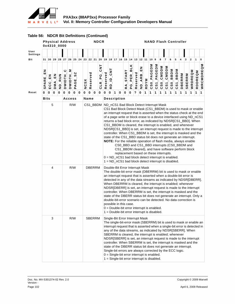
PXA3xx (88AP3xx) Processor Family Vol. II: Memory Controller Configuration Developers Manual
Doc. No. MV-S301374-02 Rev. 2.0 Version -
Copyright © 2009 Marvell
Page 102 April 6, 2009 Released
12345678910111213141516171819202122232425262728293031323334353637383940414243444546474849505152535455565758
5 R/W CS1_BBDM ND_nCS1 Bad Block Detect Interrupt MaskCS1 Bad Block Detect Mask (CS1_BBDM) is used to mask or enable an interrupt request that is asserted when the status check at the end of a page write or block erase to a device interfaced using ND_nCS1 returns a bad block error, as indicated by NDSR[CS1_BBD]. When CS1_BBDM is cleared, the interrupt is enabled, and whenever NDSR[CS1_BBD] is set, an interrupt request is made to the interrupt controller. When CS1_BBDM is set, the interrupt is masked and the state of the CS1_BBD status bit does not generate an interrupt.NOTE: For the reliable operation of flash media, always enable
CS0_BBD and CS1_BBD interrupts (CS0_BBDM and CS1_BBDM cleared), and have software perform block replacement based on these interrupts.
0 = ND_nCS1 bad block detect interrupt is enabled.1 = ND_nCS1 bad block detect interrupt is disabled.
4 R/W DBERRM Double-Bit Error Interrupt MaskThe double-bit error mask (DBERRM) bit is used to mask or enable an interrupt request that is asserted when a double-bit error is detected in any of the data streams as indicated by NDSR[DBERR]. When DBERRM is cleared, the interrupt is enabled; whenever NDSR[DBERR] is set, an interrupt request is made to the interrupt controller. When DBERRM is set, the interrupt is masked and the state of the DBERR status bit does not generate an interrupt. Only a double-bit-error scenario can be detected. No data correction is possible in this case.0 = Double-bit error interrupt is enabled.1 = Double-bit error interrupt is disabled.
3 R/W SBERRM Single-Bit Error Interrupt MaskThe single-bit-error mask (SBERRM) bit is used to mask or enable an interrupt request that is asserted when a single-bit error is detected in any of the data streams, as indicated by NDSR[SBERR]. When SBERRM is cleared, the interrupt is enabled; whenever NDSR[SBERR] is set, an interrupt request is made to the interrupt controller. When SBERRM is set, the interrupt is masked and the state of the DBERR status bit does not generate an interrupt. Single-bit errors are always corrected by the ECC logic.0 = Single-bit error interrupt is enabled.1 = Single-bit error interrupt is disabled.
Table 56: NDCR Bit Definitions (Continued)
Physical Address0x4310_0000
NDCR NAND Flash Controller
User Settings
Bit 31 30 29 28 27 26 25 24 23 22 21 20 19 18 17 16 15 14 13 12 11 10 9 8 7 6 5 4 3 2 1 0
SP
AR
E_
EN
EC
C_
EN
DM
A_
EN
ND
_R
UN
DW
IDT
H_
C
DW
IDT
H_
M
PA
GE
_S
Z
NC
SX
Re
se
rve
d
CL
R_
PG
_C
NT
Re
se
rve
d
RD
_ID
_C
NT
RA
_S
TA
RT
PG
_P
ER
_B
LK
Re
se
rve
d
ND
_A
RB
_E
N
RD
YM
CS
0_
PA
GE
DM
CS
1_
PA
GE
DM
CS
0_
CM
DD
M
CS
1_
CM
DD
M
CS
0_
BB
DM
CS
1_
BB
DM
DB
ER
RM
SB
ER
RM
WR
DR
EQ
M
RD
DR
EQ
M
WR
CM
DR
EQ
M
Reset 0 0 0 0 0 0 0 0 0 0 0 0 0 0 1 0 0 0 ? 0 1 1 1 1 1 1 1 1 1 1 1 1
Bits Access Name Descript ion

NAND Flash ControllerRegister Descriptions
Copyright © 2009 Marvell Doc. No. MV-S301374-02 Rev. 2.0Version -
April 6, 2009 Released Page 103
12345678910111213141516171819202122232425262728293031323334353637383940414243444546474849505152535455565758
3.8.3 NAND Interface Timing Parameter 0 Register (NDTR0CS0)Program the NAND Interface Timing Parameter 0 register (NDTR0CS0) to configure the setup and hold times of outputs driven by the NAND flash controller (ND_ALE, ND_CLE, ND_nCS1 and ND_nCS0) and the pulse widths and cycle times of ND_nRE and ND_nWE. Accesses to NAND flash devices interfaced using ND_nCS0 and ND_nCS1 are controlled by the settings in
2 R/W WRDREQM Write Data Request Interrupt MaskThe write-data-request mask (WRDREQM) bit is used to mask or enable an interrupt request that is asserted when a write command is loaded into command buffer and data buffer is empty, as indicated by NDSR[WRDREQ]. When WRDREQM is cleared, the interrupt is enabled; whenever NDSR[WRDREQ] is set, an interrupt request is made to the interrupt controller. When WRDREQM is set, the interrupt is masked and the state of the WRDREQ status bit does not generate an interrupt.0 = Write data request interrupt is enabled.1 = Write data request interrupt is disabled.
1 R/W RDDREQM Read Data Request Interrupt MaskRead data request mask (RDDREQM) is used to mask or enable an interrupt request that is asserted when the data buffer has been loaded with a page of read data, as indicated by NDSR[RDDREQ]. When RDDREQM is cleared, the interrupt is enabled, and whenever NDSR[RDDREQ] is set, an interrupt request is made to the interrupt controller. When RDDREQM is set, the interrupt is masked and the state of the RDDREQ status bit does not generate an interrupt.0 = Read data request interrupt is enabled.1 = Read data request interrupt is disabled.
0 R/W WRCMDREQM
Write Command Request Interrupt MaskWrite command request mask (WRCMDREQM) is used to mask or enable an interrupt request that is asserted when a write to the command buffer is requested, as indicated by NDSR[WRCMDREQ]. When WRCMDREQM is cleared, the interrupt is enabled, and whenever NDSR[WRCMDREQ] is set, an interrupt request is made to the interrupt controller. When WRCMDREQM is set, the interrupt is masked and the state of the RDDREQ status bit does not generate an interrupt.0 = Write command request interrupt is enabled.1 = Write command request interrupt is disabled.
Table 56: NDCR Bit Definitions (Continued)
Physical Address0x4310_0000
NDCR NAND Flash Controller
User Settings
Bit 31 30 29 28 27 26 25 24 23 22 21 20 19 18 17 16 15 14 13 12 11 10 9 8 7 6 5 4 3 2 1 0
SP
AR
E_
EN
EC
C_
EN
DM
A_
EN
ND
_R
UN
DW
IDT
H_
C
DW
IDT
H_
M
PA
GE
_S
Z
NC
SX
Re
se
rve
d
CL
R_
PG
_C
NT
Re
se
rve
d
RD
_ID
_C
NT
RA
_S
TA
RT
PG
_P
ER
_B
LK
Re
se
rve
d
ND
_A
RB
_E
N
RD
YM
CS
0_
PA
GE
DM
CS
1_
PA
GE
DM
CS
0_
CM
DD
M
CS
1_
CM
DD
M
CS
0_
BB
DM
CS
1_
BB
DM
DB
ER
RM
SB
ER
RM
WR
DR
EQ
M
RD
DR
EQ
M
WR
CM
DR
EQ
M
Reset 0 0 0 0 0 0 0 0 0 0 0 0 0 0 1 0 0 0 ? 0 1 1 1 1 1 1 1 1 1 1 1 1
Bits Access Name Descript ion
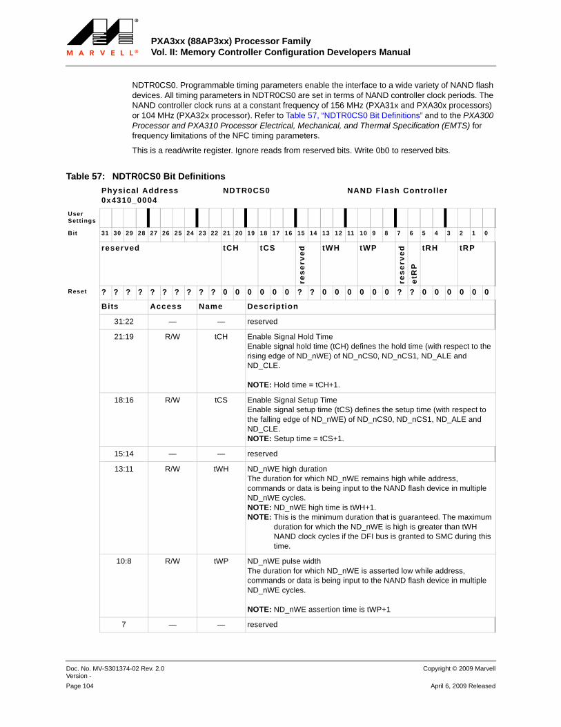
PXA3xx (88AP3xx) Processor Family Vol. II: Memory Controller Configuration Developers Manual
Doc. No. MV-S301374-02 Rev. 2.0 Version -
Copyright © 2009 Marvell
Page 104 April 6, 2009 Released
12345678910111213141516171819202122232425262728293031323334353637383940414243444546474849505152535455565758
NDTR0CS0. Programmable timing parameters enable the interface to a wide variety of NAND flash devices. All timing parameters in NDTR0CS0 are set in terms of NAND controller clock periods. The NAND controller clock runs at a constant frequency of 156 MHz (PXA31x and PXA30x processors) or 104 MHz (PXA32x processor). Refer to Table 57, “NDTR0CS0 Bit Definitions” and to the PXA300 Processor and PXA310 Processor Electrical, Mechanical, and Thermal Specification (EMTS) for frequency limitations of the NFC timing parameters.
This is a read/write register. Ignore reads from reserved bits. Write 0b0 to reserved bits.
Table 57: NDTR0CS0 Bit Definitions
Physical Address0x4310_0004
NDTR0CS0 NAND Flash Controller
User Settings
Bit 31 30 29 28 27 26 25 24 23 22 21 20 19 18 17 16 15 14 13 12 11 10 9 8 7 6 5 4 3 2 1 0
reserved tCH tCS
res
erv
ed tWH tWP
res
erv
ed
etR
P
tRH tRP
Reset ? ? ? ? ? ? ? ? ? ? 0 0 0 0 0 0 ? ? 0 0 0 0 0 0 ? ? 0 0 0 0 0 0
Bits Access Name Description
31:22 — — reserved
21:19 R/W tCH Enable Signal Hold TimeEnable signal hold time (tCH) defines the hold time (with respect to the rising edge of ND_nWE) of ND_nCS0, ND_nCS1, ND_ALE and ND_CLE.
NOTE: Hold time = tCH+1.
18:16 R/W tCS Enable Signal Setup Time Enable signal setup time (tCS) defines the setup time (with respect to the falling edge of ND_nWE) of ND_nCS0, ND_nCS1, ND_ALE and ND_CLE. NOTE: Setup time = tCS+1.
15:14 — — reserved
13:11 R/W tWH ND_nWE high durationThe duration for which ND_nWE remains high while address, commands or data is being input to the NAND flash device in multiple ND_nWE cycles.NOTE: ND_nWE high time is tWH+1.NOTE: This is the minimum duration that is guaranteed. The maximum
duration for which the ND_nWE is high is greater than tWH NAND clock cycles if the DFI bus is granted to SMC during this time.
10:8 R/W tWP ND_nWE pulse widthThe duration for which ND_nWE is asserted low while address, commands or data is being input to the NAND flash device in multiple ND_nWE cycles.
NOTE: ND_nWE assertion time is tWP+1
7 — — reserved
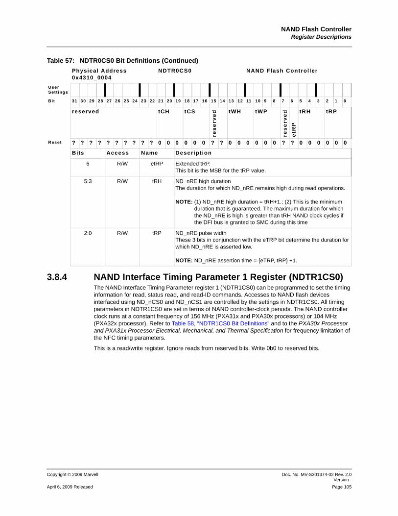
NAND Flash ControllerRegister Descriptions
Copyright © 2009 Marvell Doc. No. MV-S301374-02 Rev. 2.0Version -
April 6, 2009 Released Page 105
12345678910111213141516171819202122232425262728293031323334353637383940414243444546474849505152535455565758
3.8.4 NAND Interface Timing Parameter 1 Register (NDTR1CS0)The NAND Interface Timing Parameter register 1 (NDTR1CS0) can be programmed to set the timing information for read, status read, and read-ID commands. Accesses to NAND flash devices interfaced using ND_nCS0 and ND_nCS1 are controlled by the settings in NDTR1CS0. All timing parameters in NDTR1CS0 are set in terms of NAND controller-clock periods. The NAND controller clock runs at a constant frequency of 156 MHz (PXA31x and PXA30x processors) or 104 MHz (PXA32x processor). Refer to Table 58, “NDTR1CS0 Bit Definitions” and to the PXA30x Processor and PXA31x Processor Electrical, Mechanical, and Thermal Specification for frequency limitation of the NFC timing parameters.
This is a read/write register. Ignore reads from reserved bits. Write 0b0 to reserved bits.
6 R/W etRP Extended tRP. This bit is the MSB for the tRP value.
5:3 R/W tRH ND_nRE high durationThe duration for which ND_nRE remains high during read operations.
NOTE: (1) ND_nRE high duration = tRH+1.; (2) This is the minimum duration that is guaranteed. The maximum duration for which the ND_nRE is high is greater than tRH NAND clock cycles if the DFI bus is granted to SMC during this time
2:0 R/W tRP ND_nRE pulse widthThese 3 bits in conjunction with the eTRP bit determine the duration for which ND_nRE is asserted low.
NOTE: ND_nRE assertion time = {eTRP, tRP} +1.
Table 57: NDTR0CS0 Bit Definitions (Continued)
Physical Address0x4310_0004
NDTR0CS0 NAND Flash Controller
User Settings
Bit 31 30 29 28 27 26 25 24 23 22 21 20 19 18 17 16 15 14 13 12 11 10 9 8 7 6 5 4 3 2 1 0
reserved tCH tCS
res
erv
ed tWH tWP
res
erv
ed
etR
P
tRH tRP
Reset ? ? ? ? ? ? ? ? ? ? 0 0 0 0 0 0 ? ? 0 0 0 0 0 0 ? ? 0 0 0 0 0 0
Bits Access Name Description

PXA3xx (88AP3xx) Processor Family Vol. II: Memory Controller Configuration Developers Manual
Doc. No. MV-S301374-02 Rev. 2.0 Version -
Copyright © 2009 Marvell
Page 106 April 6, 2009 Released
12345678910111213141516171819202122232425262728293031323334353637383940414243444546474849505152535455565758
3.8.5 NAND Controller Status Register (NDSR)The NAND Controller Status register (NDSR) contains bits that signal flash ready status, bad-block detected, read-data-error conditions, data-read/write requests, completion of a page, and command.
Table 58: NDTR1CS0 Bit Definitions
Physical Address0x4310_000C
NDTR1CS0 NAND Flash Controller
User Settings
Bit 31 30 29 28 27 26 25 24 23 22 21 20 19 18 17 16 15 14 13 12 11 10 9 8 7 6 5 4 3 2 1 0
tR reserved tWHR tAR
Reset 0 0 0 0 0 0 0 0 0 0 0 0 0 0 0 0 ? ? ? ? ? ? ? ? 0 0 0 0 0 0 0 0
Bits Access Name Descript ion
31:16 R/W tR ND_nWE high to ND_nRE Low for ReadSpecifies the delay between ND_nWE high and ND_nRE low for reads. This delay depends on the value programmed in NDTR0CS0[tCH] in addition to tR programmed value.
NOTE: Delay = (tCH + 1) + (tR+2)
NOTE: The ND_RnB signal is not monitored by the controller (low to high transition) during read operations. Software needs to ensure that tR is programmed correctly to meet the NAND timing requirements for ND_nRE assertion timing. The RDY status still gets set when the device becomes Ready but the controller does not respond to it.
15:8 — — reserved
7:4 R/W tWHR ND_nWE High to ND_nRE Low for a Read Status or Read IDFor a read-status or read-ID commands, ND_nWE high to ND_nRE Low Delay (tWHR) specifies the delay between de-assertion of ND_nWE and assertion of ND_nRE. NOTE: The actual delay between ND_nWE de-assertion and
ND_nRE assertion is tWHR+1 NAND controller clock cycles as long as tWHR is greater than tAR + tCH as described below.
NOTE: (1) Delay = (tCH + tAR+2) if (tAR + tCH) >= tWHR; (2) Delay = (tWHR+ 1) if (tAR + tCH) < tWHR; (3) This is the minimum duration that is guaranteed. If the DFI bus is granted to SMEMC during this time the delay will be longer.
3:0 R/W tAR ND_ALE Low to ND_nRE Low Delay For a read-status or read-ID command, ND_ALE Low to ND_nRE Low delay (tAR) specifies the delay between de-assertion of ND_ALE and assertion of ND_nRE. NOTE: The actual delay between ND_ALE de-assertion and
ND_nRE assertion is tAR+1 NAND controller clock cycles as long as tWHR isn’t greater than tAR + tCH as described below.
NOTE: (1) Delay = (tAR+1) if (tAR + tCH) >= tWHR; (2) Delay = (tWHR - tCH) if (tAR + tCH) < tWHR; (3) This is the minimum duration that is guaranteed. If the DFI bus is granted to the SMC during this time these delay will be longer.

NAND Flash ControllerRegister Descriptions
Copyright © 2009 Marvell Doc. No. MV-S301374-02 Rev. 2.0Version -
April 6, 2009 Released Page 107
12345678910111213141516171819202122232425262728293031323334353637383940414243444546474849505152535455565758
Unless masked, each of these hardware-detected events signals an interrupt request to the interrupt controller. Once set, each of the status bits is cleared by writing 0b1 to the corresponding bit position. Writing 0b0 has no effect on the status bits. Each of the NDSR bits signals an interrupt request as long as the bit is set and the corresponding interrupt is not masked. Once the bit is cleared, the interrupt is cleared.
NDSR status bits are set in both DMA and non-DMA modes of operation, and they can be polled and cleared by software in either mode. Refer to Table 59 for details.
This is a read/write register. Ignore reads from reserved bits. Write 0b0 to reserved bits.
Table 59: NDSR Bit Definitions
Physical Address0x4310_0014
NDSR NAND Flash Controller
User Settings
Bit 31 30 29 28 27 26 25 24 23 22 21 20 19 18 17 16 15 14 13 12 11 10 9 8 7 6 5 4 3 2 1 0
reserved
RD
Y
CS
0_
PA
GE
D
CS
1_
PA
GE
D
CS
0_
CM
DD
CS
1_
CM
DD
CS
0_
BB
D
CS
1_
BB
D
DB
ER
R
SB
ER
R
WR
DR
EQ
RD
DR
EQ
WR
CM
DR
EQ
Reset ? ? ? ? ? ? ? ? ? ? ? ? ? ? ? ? ? ? ? ? 0 0 0 0 0 0 0 0 0 0 0 0
Bits Access Name Description
31:12 — — reserved
11 R/Write 1 toclear
RDY NAND Flash ReadyThe NAND flash-ready (RDY) status bit is set when NAND_RnB (NAND Flash Ready/Busy) has made a low-to-high transition, indicating the ready state entry of flash device(s). The NAND flash-ready condition can be programmed to cause an interrupt by clearing the flash-device-ready interrupt mask (RDYM). This status bit is updated continuously each time NAND_RnB input makes a low-to-high transition, regardless of the type of command sent to the flash device.
0 = The Ready/Busy_ input has not transitioned from low to high.1 = The Ready/Busy_ input has transitioned from low to highNOTE: If the RnB signal is pulled low prior to entering any Low power
mode (refer to the Clock Controller and Power Management chapter in Volume I), the edge detect on the pad register also needs to be cleared, so a false RnB edge transition is not detected.
NOTE: When coming out of a low power mode, the RDY bit of the NDSR register is set if a low-to-high transition of the RnB signal is detected or if the RnB signal stayed low prior to entering the mode. Conversely, the RDY bit of the NDSR register is not set if there is no low-to-high RnB transition and RnB is not low prior to entering the low power mode.

PXA3xx (88AP3xx) Processor Family Vol. II: Memory Controller Configuration Developers Manual
Doc. No. MV-S301374-02 Rev. 2.0 Version -
Copyright © 2009 Marvell
Page 108 April 6, 2009 Released
12345678910111213141516171819202122232425262728293031323334353637383940414243444546474849505152535455565758
10 R/Write 1 toclear
CS0_PAGED
ND_nCS0 Page DoneThe CS0 page-done (CS0_PAGED) status bit is set when the read or write transaction to flash device(s) interfaced using ND_nCS0 has completed a page of access including any user-defined spare-area access and ECC. CS0_PAGED is not set if an auto-status check after a program command results in a failure. CS0_PAGED bit is not set for read ID, read status, and erase commands. Page-done condition can be programmed to cause an interrupt by clearing the page- done interrupt mask (CS0_PAGEDM). 0 = The current read/write transaction on ND_nCS0 has not reached a page boundary.1 = The current read/write transaction on ND_nCS0 has reached a page boundary.
9 R/Write 1 toclear
CS1_PAGED
ND_nCS1 Page DoneThe ND_nCS1 page-done (CS1_PAGED) status bit is set when the read or write transaction to flash device(s) interfaced using ND_nCS1 has completed a page of access including any user- defined spare-area access and ECC. CS1_PAGED is not set if an auto-status check after a program command results in a failure. The CS1_PAGED bit is not set for read ID, read status, and erase commands. Page-done condition can be programmed to cause an interrupt by clearing the page- done interrupt mask (CS1_PAGEDM). NOTE: Page-done status bits (CS0_PAGED and CS1_PAGED)
should be used only for a page-related command like read or write. These bits should be ignored when they get set for erase commands. The following work around can be used so that page-done bits do not get set for erase.
• Do not enable AUTO_SR bit for erase commands• The command immediately following an erase command should
always be a read-status command.• Do not set AUTO_SR bit for this read-status command.0 = The current read/write transaction on ND_nCS1 has not reached a page boundary.1 = The current read/write transaction on ND_nCS1 has reached a page boundary.
Table 59: NDSR Bit Definitions (Continued)
Physical Address0x4310_0014
NDSR NAND Flash Controller
User Settings
Bit 31 30 29 28 27 26 25 24 23 22 21 20 19 18 17 16 15 14 13 12 11 10 9 8 7 6 5 4 3 2 1 0
reserved
RD
Y
CS
0_
PA
GE
D
CS
1_
PA
GE
D
CS
0_
CM
DD
CS
1_
CM
DD
CS
0_
BB
D
CS
1_
BB
D
DB
ER
R
SB
ER
R
WR
DR
EQ
RD
DR
EQ
WR
CM
DR
EQ
Reset ? ? ? ? ? ? ? ? ? ? ? ? ? ? ? ? ? ? ? ? 0 0 0 0 0 0 0 0 0 0 0 0
Bits Access Name Description
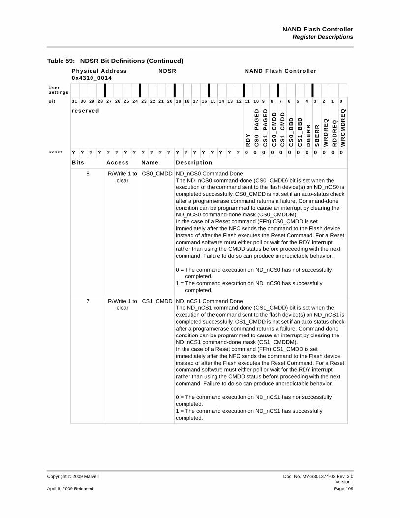
NAND Flash ControllerRegister Descriptions
Copyright © 2009 Marvell Doc. No. MV-S301374-02 Rev. 2.0Version -
April 6, 2009 Released Page 109
12345678910111213141516171819202122232425262728293031323334353637383940414243444546474849505152535455565758
8 R/Write 1 toclear
CS0_CMDD ND_nCS0 Command DoneThe ND_nCS0 command-done (CS0_CMDD) bit is set when the execution of the command sent to the flash device(s) on ND_nCS0 is completed successfully. CS0_CMDD is not set if an auto-status check after a program/erase command returns a failure. Command-done condition can be programmed to cause an interrupt by clearing the ND_nCS0 command-done mask (CS0_CMDDM).In the case of a Reset command (FFh) CS0_CMDD is set immediately after the NFC sends the command to the Flash device instead of after the Flash executes the Reset Command. For a Reset command software must either poll or wait for the RDY interrupt rather than using the CMDD status before proceeding with the next command. Failure to do so can produce unpredictable behavior.
0 = The command execution on ND_nCS0 has not successfully completed.
1 = The command execution on ND_nCS0 has successfully completed.
7 R/Write 1 toclear
CS1_CMDD ND_nCS1 Command DoneThe ND_nCS1 command-done (CS1_CMDD) bit is set when the execution of the command sent to the flash device(s) on ND_nCS1 is completed successfully. CS1_CMDD is not set if an auto-status check after a program/erase command returns a failure. Command-done condition can be programmed to cause an interrupt by clearing the ND_nCS1 command-done mask (CS1_CMDDM).In the case of a Reset command (FFh) CS1_CMDD is set immediately after the NFC sends the command to the Flash device instead of after the Flash executes the Reset Command. For a Reset command software must either poll or wait for the RDY interrupt rather than using the CMDD status before proceeding with the next command. Failure to do so can produce unpredictable behavior.
0 = The command execution on ND_nCS1 has not successfully completed.1 = The command execution on ND_nCS1 has successfully completed.
Table 59: NDSR Bit Definitions (Continued)
Physical Address0x4310_0014
NDSR NAND Flash Controller
User Settings
Bit 31 30 29 28 27 26 25 24 23 22 21 20 19 18 17 16 15 14 13 12 11 10 9 8 7 6 5 4 3 2 1 0
reserved
RD
Y
CS
0_
PA
GE
D
CS
1_
PA
GE
D
CS
0_
CM
DD
CS
1_
CM
DD
CS
0_
BB
D
CS
1_
BB
D
DB
ER
R
SB
ER
R
WR
DR
EQ
RD
DR
EQ
WR
CM
DR
EQ
Reset ? ? ? ? ? ? ? ? ? ? ? ? ? ? ? ? ? ? ? ? 0 0 0 0 0 0 0 0 0 0 0 0
Bits Access Name Description

PXA3xx (88AP3xx) Processor Family Vol. II: Memory Controller Configuration Developers Manual
Doc. No. MV-S301374-02 Rev. 2.0 Version -
Copyright © 2009 Marvell
Page 110 April 6, 2009 Released
12345678910111213141516171819202122232425262728293031323334353637383940414243444546474849505152535455565758
6 R/Write 1 toclear
CS0_BBD ND_nCS0 Bad Block DetectThe ND_nCS0 bad-block detect (CS0_BBD) status bit is set when the status read after a program/erase operation to flash device(s) interfaced using ND_nCS0 returns a program/erase failure. A bad-block detect condition can be programmed to cause an interrupt by clearing the ND_nCS0 bad-block detect interrupt mask (CS0_BBDM). When two 8-bit NAND flash devices are interfaced to the 16-bit NFC DFI bus (NDCR[DWIDTH_C] = 1 and NDCR[DWIDTH_M] = 0) using ND_nCS0, a program/erase failure in any one of the two devices results in the CS0_BBD bit getting set. Because both flash devices are addressed at the same time, software must mark the corresponding blocks as non-valid. 0 = No bad block is encountered while a write/erase on ND_nCS01 = Bad block is encountered while a write/erase on ND_nCS0
5 R/Write 1 toclear
CS1_BBD ND_nCS1 Bad Block DetectThe ND_nCS1 bad-block detect (CS1_BBD) status bit is set when the status read after a program/erase operation to flash device(s) interfaced using ND_nCS1 returns a program/erase failure. A bad-block detect condition can be programmed to cause an interrupt by clearing the ND_nCS1 bad block detect interrupt mask (CS1_BBDM). When two 8-bit NAND flash devices are interfaced to the 16-bit NFC DFI bus (NDCR[DWIDTH_C]= 1 and NDCR[DWIDTH_M] = 0) using ND_nCS1, a program/erase failure in any one of the two devices results in CS1_BBD bit getting set. Because both flash devices are addressed at the same time, software can mark the corresponding blocks as non-valid. 0 = No bad block is encountered while a write/erase on ND_nCS11 = Bad block is encountered while a write/erase on ND_nCS1
Table 59: NDSR Bit Definitions (Continued)
Physical Address0x4310_0014
NDSR NAND Flash Controller
User Settings
Bit 31 30 29 28 27 26 25 24 23 22 21 20 19 18 17 16 15 14 13 12 11 10 9 8 7 6 5 4 3 2 1 0
reserved
RD
Y
CS
0_
PA
GE
D
CS
1_
PA
GE
D
CS
0_
CM
DD
CS
1_
CM
DD
CS
0_
BB
D
CS
1_
BB
D
DB
ER
R
SB
ER
R
WR
DR
EQ
RD
DR
EQ
WR
CM
DR
EQ
Reset ? ? ? ? ? ? ? ? ? ? ? ? ? ? ? ? ? ? ? ? 0 0 0 0 0 0 0 0 0 0 0 0
Bits Access Name Description
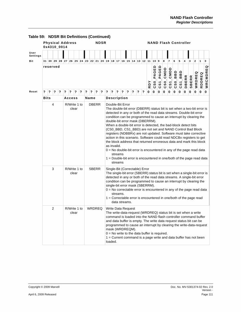
NAND Flash ControllerRegister Descriptions
Copyright © 2009 Marvell Doc. No. MV-S301374-02 Rev. 2.0Version -
April 6, 2009 Released Page 111
12345678910111213141516171819202122232425262728293031323334353637383940414243444546474849505152535455565758
4 R/Write 1 toclear
DBERR Double-Bit ErrorThe double-bit error (DBERR) status bit is set when a two-bit error is detected in any or both of the read data streams. Double-bit error condition can be programmed to cause an interrupt by clearing the double-bit error mask (DBERRM).When a double-bit error is detected, the bad-block detect bits (CS0_BBD, CS1_BBD) are not set and NAND Control Bad Block registers (NDBBRx) are not updated. Software must take corrective action in this scenario. Software could read NDCBx registers to get the block address that returned erroneous data and mark this block as invalid.0 = No double-bit error is encountered in any of the page read data
streams1 = Double-bit error is encountered in one/both of the page read data
streams
3 R/Write 1 toclear
SBERR Single-Bit (Correctable) ErrorThe single-bit error (SBERR) status bit is set when a single-bit error is detected in any or both of the read data streams. A single-bit error condition can be programmed to cause an interrupt by clearing the single-bit error mask (SBERRM).0 = No correctable error is encountered in any of the page read data
streams.1 = Correctable error is encountered in one/both of the page read
data streams.
2 R/Write 1 toclear
WRDREQ Write Data RequestThe write-data-request (WRDREQ) status bit is set when a write command is loaded into the NAND flash controller command buffer and data buffer is empty. The write data request status bit can be programmed to cause an interrupt by clearing the write-data-request mask (WRDREQM). 0 = No write to the data buffer is required.1 = Current command is a page write and data buffer has not been loaded.
Table 59: NDSR Bit Definitions (Continued)
Physical Address0x4310_0014
NDSR NAND Flash Controller
User Settings
Bit 31 30 29 28 27 26 25 24 23 22 21 20 19 18 17 16 15 14 13 12 11 10 9 8 7 6 5 4 3 2 1 0
reserved
RD
Y
CS
0_
PA
GE
D
CS
1_
PA
GE
D
CS
0_
CM
DD
CS
1_
CM
DD
CS
0_
BB
D
CS
1_
BB
D
DB
ER
R
SB
ER
R
WR
DR
EQ
RD
DR
EQ
WR
CM
DR
EQ
Reset ? ? ? ? ? ? ? ? ? ? ? ? ? ? ? ? ? ? ? ? 0 0 0 0 0 0 0 0 0 0 0 0
Bits Access Name Description
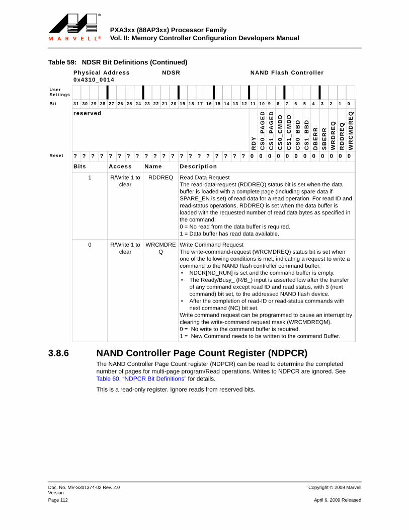
PXA3xx (88AP3xx) Processor Family Vol. II: Memory Controller Configuration Developers Manual
Doc. No. MV-S301374-02 Rev. 2.0 Version -
Copyright © 2009 Marvell
Page 112 April 6, 2009 Released
12345678910111213141516171819202122232425262728293031323334353637383940414243444546474849505152535455565758
3.8.6 NAND Controller Page Count Register (NDPCR)The NAND Controller Page Count register (NDPCR) can be read to determine the completed number of pages for multi-page program/Read operations. Writes to NDPCR are ignored. See Table 60, “NDPCR Bit Definitions” for details.
This is a read-only register. Ignore reads from reserved bits.
1 R/Write 1 toclear
RDDREQ Read Data RequestThe read-data-request (RDDREQ) status bit is set when the data buffer is loaded with a complete page (including spare data if SPARE_EN is set) of read data for a read operation. For read ID and read-status operations, RDDREQ is set when the data buffer is loaded with the requested number of read data bytes as specified in the command.0 = No read from the data buffer is required.1 = Data buffer has read data available.
0 R/Write 1 toclear
WRCMDREQ
Write Command RequestThe write-command-request (WRCMDREQ) status bit is set when one of the following conditions is met, indicating a request to write a command to the NAND flash controller command buffer.• NDCR[ND_RUN] is set and the command buffer is empty. • The Ready/Busy_ (R/B_) input is asserted low after the transfer
of any command except read ID and read status, with 3 (next command) bit set, to the addressed NAND flash device.
• After the completion of read-ID or read-status commands with next command (NC) bit set.
Write command request can be programmed to cause an interrupt by clearing the write-command request mask (WRCMDREQM).0 = No write to the command buffer is required.1 = New Command needs to be written to the command Buffer.
Table 59: NDSR Bit Definitions (Continued)
Physical Address0x4310_0014
NDSR NAND Flash Controller
User Settings
Bit 31 30 29 28 27 26 25 24 23 22 21 20 19 18 17 16 15 14 13 12 11 10 9 8 7 6 5 4 3 2 1 0
reserved
RD
Y
CS
0_
PA
GE
D
CS
1_
PA
GE
D
CS
0_
CM
DD
CS
1_
CM
DD
CS
0_
BB
D
CS
1_
BB
D
DB
ER
R
SB
ER
R
WR
DR
EQ
RD
DR
EQ
WR
CM
DR
EQ
Reset ? ? ? ? ? ? ? ? ? ? ? ? ? ? ? ? ? ? ? ? 0 0 0 0 0 0 0 0 0 0 0 0
Bits Access Name Description
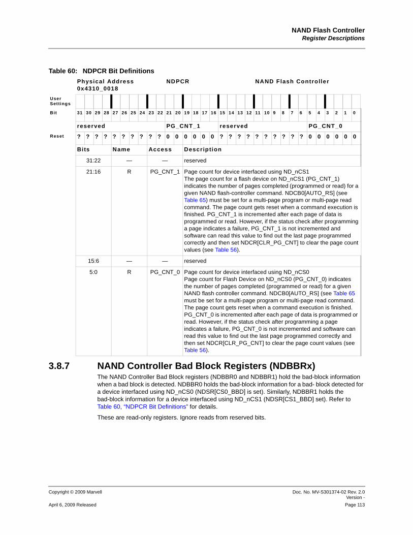
NAND Flash ControllerRegister Descriptions
Copyright © 2009 Marvell Doc. No. MV-S301374-02 Rev. 2.0Version -
April 6, 2009 Released Page 113
12345678910111213141516171819202122232425262728293031323334353637383940414243444546474849505152535455565758
3.8.7 NAND Controller Bad Block Registers (NDBBRx)The NAND Controller Bad Block registers (NDBBR0 and NDBBR1) hold the bad-block information when a bad block is detected. NDBBR0 holds the bad-block information for a bad- block detected for a device interfaced using ND_nCS0 (NDSR[CS0_BBD] is set). Similarly, NDBBR1 holds the bad-block information for a device interfaced using ND_nCS1 (NDSR[CS1_BBD] set). Refer to Table 60, “NDPCR Bit Definitions” for details.
These are read-only registers. Ignore reads from reserved bits.
Table 60: NDPCR Bit Definitions
Physical Address0x4310_0018
NDPCR NAND Flash Controller
User Settings
Bit 31 30 29 28 27 26 25 24 23 22 21 20 19 18 17 16 15 14 13 12 11 10 9 8 7 6 5 4 3 2 1 0
reserved PG_CNT_1 reserved PG_CNT_0
Reset ? ? ? ? ? ? ? ? ? ? 0 0 0 0 0 0 ? ? ? ? ? ? ? ? ? ? 0 0 0 0 0 0
Bits Name Access Description
31:22 — — reserved
21:16 R PG_CNT_1 Page count for device interfaced using ND_nCS1The page count for a flash device on ND_nCS1 (PG_CNT_1) indicates the number of pages completed (programmed or read) for a given NAND flash-controller command. NDCB0[AUTO_RS] (see Table 65) must be set for a multi-page program or multi-page read command. The page count gets reset when a command execution is finished. PG_CNT_1 is incremented after each page of data is programmed or read. However, if the status check after programming a page indicates a failure, PG_CNT_1 is not incremented and software can read this value to find out the last page programmed correctly and then set NDCR[CLR_PG_CNT] to clear the page count values (see Table 56).
15:6 — — reserved
5:0 R PG_CNT_0 Page count for device interfaced using ND_nCS0Page count for Flash Device on ND_nCS0 (PG_CNT_0) indicates the number of pages completed (programmed or read) for a given NAND flash controller command. NDCB0[AUTO_RS] (see Table 65 must be set for a multi-page program or multi-page read command. The page count gets reset when a command execution is finished. PG_CNT_0 is incremented after each page of data is programmed or read. However, if the status check after programming a page indicates a failure, PG_CNT_0 is not incremented and software can read this value to find out the last page programmed correctly and then set NDCR[CLR_PG_CNT] to clear the page count values (see Table 56).

PXA3xx (88AP3xx) Processor Family Vol. II: Memory Controller Configuration Developers Manual
Doc. No. MV-S301374-02 Rev. 2.0 Version -
Copyright © 2009 Marvell
Page 114 April 6, 2009 Released
12345678910111213141516171819202122232425262728293031323334353637383940414243444546474849505152535455565758
3.8.8 NAND Read Enable Return Delay Register (NDREDEL) (PXA30x and PXA31x Processors Only)The NAND Read Enable Return Delay register (NDREDEL) is used to specify the amount of delay added to the latching edge of ND_nRE during Reads of NAND devices. The Return Clock Unit consists of a chain of eight programmable delay units. The bits of NDREDEL are input to the Return Clk Unit to program these delay units and also to select which delay unit output is used to latch Read data. Bits 31 to 28 are reserved. Bits 27 to 24 are used to select the preferred delay unit output. Bits 23 to 0, divided into eight sets of three successive bits each, store the information for controlling the amount of delay for each of the eight delay units, respectively. Table 62 shows a mapping of expected delays introduced by the Return Clock Unit given different values for NDREDEL[27:0].
Table 61: NDBBRx Bit Definitions
Physical Address0x4310_001C0x4310_0020
NDBBRx NAND Flash Control ler
User Settings
Bit 31 30 29 28 27 26 25 24 23 22 21 20 19 18 17 16 15 14 13 12 11 10 9 8 7 6 5 4 3 2 1 0
Bad Block Information
Reset 0 0 0 0 0 0 0 0 0 0 0 0 0 0 0 0 0 0 0 0 0 0 0 0 0 0 0 0 0 0 0 0
Bits Access Name Descript ion
31:0 R Bad Block Information
Bad block information contained in these registers consists of ADDR5, ADDR4, ADDR3, and ADDR2 for the command that resulted in a bad block detection. ADDR5 occupies the most significant byte and ADDR2 the least significant byte in NDBDRx. When a bad block is detected (the CS0_BBD or CS1_BBD bits in NDSR gets set), software reads the corresponding NDBDRx registers, uses the relevant portions of the bad-block information to get the bad-block address, and mark these blocks addresses as non-valid. Writes to the NDBBRx registers are ignored.
Table 62: NDREDEL Bit Definitions
Physical Address0x4310_0024
NDREDEL NAND Flash Control ler
User Settings
Bit 31 30 29 28 27 26 25 24 23 22 21 20 19 18 17 16 15 14 13 12 11 10 9 8 7 6 5 4 3 2 1 0
res
erv
ed
nd
_re
_s
el
nd
_re
_d
el_
7
nd
_re
_d
el_
6
nd
_re
_d
el_
5
nd
_re
_d
el_
4
nd
_re
_d
el_
3
nd
_re
_d
el_
2
nd
_re
_d
el_
1
nd
_re
_d
el_
0
Reset ? ? ? ? 0 0 0 0 0 0 0 0 0 0 0 0 0 0 0 0 0 0 0 0 0 0 0 0 0 0 0 0
Bits Access Name Descript ion
31:28 — — Reserved
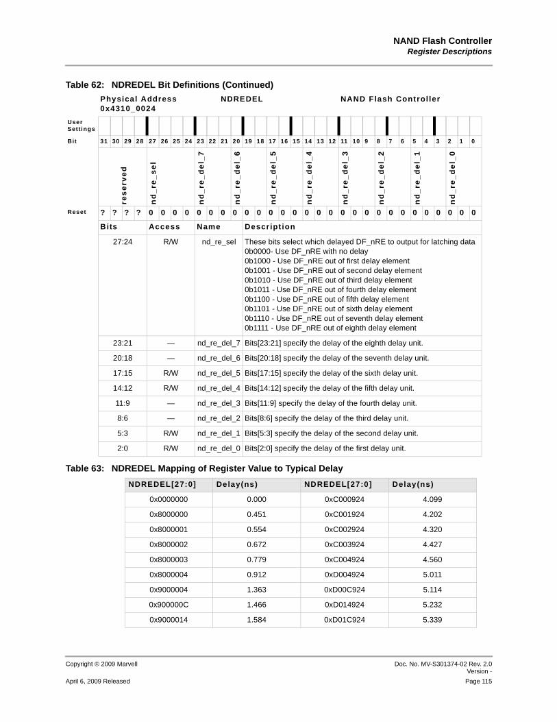
NAND Flash ControllerRegister Descriptions
Copyright © 2009 Marvell Doc. No. MV-S301374-02 Rev. 2.0Version -
April 6, 2009 Released Page 115
12345678910111213141516171819202122232425262728293031323334353637383940414243444546474849505152535455565758
27:24 R/W nd_re_sel These bits select which delayed DF_nRE to output for latching data0b0000- Use DF_nRE with no delay0b1000 - Use DF_nRE out of first delay element0b1001 - Use DF_nRE out of second delay element0b1010 - Use DF_nRE out of third delay element0b1011 - Use DF_nRE out of fourth delay element0b1100 - Use DF_nRE out of fifth delay element0b1101 - Use DF_nRE out of sixth delay element0b1110 - Use DF_nRE out of seventh delay element0b1111 - Use DF_nRE out of eighth delay element
23:21 — nd_re_del_7 Bits[23:21] specify the delay of the eighth delay unit.
20:18 — nd_re_del_6 Bits[20:18] specify the delay of the seventh delay unit.
17:15 R/W nd_re_del_5 Bits[17:15] specify the delay of the sixth delay unit.
14:12 R/W nd_re_del_4 Bits[14:12] specify the delay of the fifth delay unit.
11:9 — nd_re_del_3 Bits[11:9] specify the delay of the fourth delay unit.
8:6 — nd_re_del_2 Bits[8:6] specify the delay of the third delay unit.
5:3 R/W nd_re_del_1 Bits[5:3] specify the delay of the second delay unit.
2:0 R/W nd_re_del_0 Bits[2:0] specify the delay of the first delay unit.
Table 63: NDREDEL Mapping of Register Value to Typical Delay
NDREDEL[27:0] Delay(ns) NDREDEL[27:0] Delay(ns)
0x0000000 0.000 0xC000924 4.099
0x8000000 0.451 0xC001924 4.202
0x8000001 0.554 0xC002924 4.320
0x8000002 0.672 0xC003924 4.427
0x8000003 0.779 0xC004924 4.560
0x8000004 0.912 0xD004924 5.011
0x9000004 1.363 0xD00C924 5.114
0x900000C 1.466 0xD014924 5.232
0x9000014 1.584 0xD01C924 5.339
Table 62: NDREDEL Bit Definitions (Continued)
Physical Address0x4310_0024
NDREDEL NAND Flash Control ler
User Settings
Bit 31 30 29 28 27 26 25 24 23 22 21 20 19 18 17 16 15 14 13 12 11 10 9 8 7 6 5 4 3 2 1 0
res
erv
ed
nd
_re
_s
el
nd
_re
_d
el_
7
nd
_re
_d
el_
6
nd
_re
_d
el_
5
nd
_re
_d
el_
4
nd
_re
_d
el_
3
nd
_re
_d
el_
2
nd
_re
_d
el_
1
nd
_re
_d
el_
0
Reset ? ? ? ? 0 0 0 0 0 0 0 0 0 0 0 0 0 0 0 0 0 0 0 0 0 0 0 0 0 0 0 0
Bits Access Name Descript ion

PXA3xx (88AP3xx) Processor Family Vol. II: Memory Controller Configuration Developers Manual
Doc. No. MV-S301374-02 Rev. 2.0 Version -
Copyright © 2009 Marvell
Page 116 April 6, 2009 Released
12345678910111213141516171819202122232425262728293031323334353637383940414243444546474849505152535455565758
3.8.9 NAND Controller Data Buffer (NDDB)NAND controller data buffer (NDDB) is the read/write port of the NAND controller data buffer. NDDB is the source for Read-data DMA, and the destination for Write-data DMA. In DMA-Disabled mode, the PXA30x processor or PXA31x processor can access NDDB. Only four byte Writes and four byte Reads are supported for core accesses to NDDB. Read/write operations to NDDB must occur in the following order: The first Write corresponds to the lower four bytes of the data buffer and the following operation corresponds to the upper four bytes. Refer to Table 64 for details.
This is a read/write register. Ignore reads from reserved bits. Write 0b0 to reserved bits.
3.8.10 NAND Controller Command Buffers (NDCBx)The NAND controller-command buffers (NDCBx) hold the command currently being executed by the NAND flash controller. NAND controller-command buffer 0 (NDCB0) is the destination for command DMA. Set up command DMA to transfer 12 bytes of command to NDCB0. First four bytes are loaded to NDCB0, next four in NDCB1, and the last four bytes are loaded to NDCB2. In DMA-disabled mode, the core can write the 12 bytes of commands directly to NDCB0, four bytes at a time, which results in NDCB0, NDCB1, and NDCB2 registers getting loaded with four bytes each as explained
0x900001C 1.691 0xD024924 5.472
0x9000024 1.824 0xE024924 5.923
0xA000024 2.275 0xE064924 6.026
0xA000064 2.378 0xE0A4924 6.144
0xA0000A4 2.496 0xE0E4924 6.251
0xA0000E4 2.603 0xE124924 6.384
0xA000124 2.736 0xF124924 6.835
0xB000124 3.187 0xF324924 6.938
0xB000324 3.290 0xF524924 7.056
0xB000524 3.408 0xF724924 7.163
0xB000724 3.515 0xF924924 7.296
0xB000924 3.648
Table 63: NDREDEL Mapping of Register Value to Typical Delay (Continued)
NDREDEL[27:0] Delay(ns) NDREDEL[27:0] Delay(ns)
Table 64: NDDB Bit Definitions
Physical Address0x4310_0040
NDDB NAND Flash Controller
User Settings
Bit 31 30 29 28 27 26 25 24 23 22 21 20 19 18 17 16 15 14 13 12 11 10 9 8 7 6 5 4 3 2 1 0
NAND Flash Data
Reset 0 0 0 0 0 0 0 0 0 0 0 0 0 0 0 0 0 0 0 0 0 0 0 0 0 0 0 0 0 0 0 0
Bits Access Name Description
31:0 R/W NAND flash data
Holds the write/read data
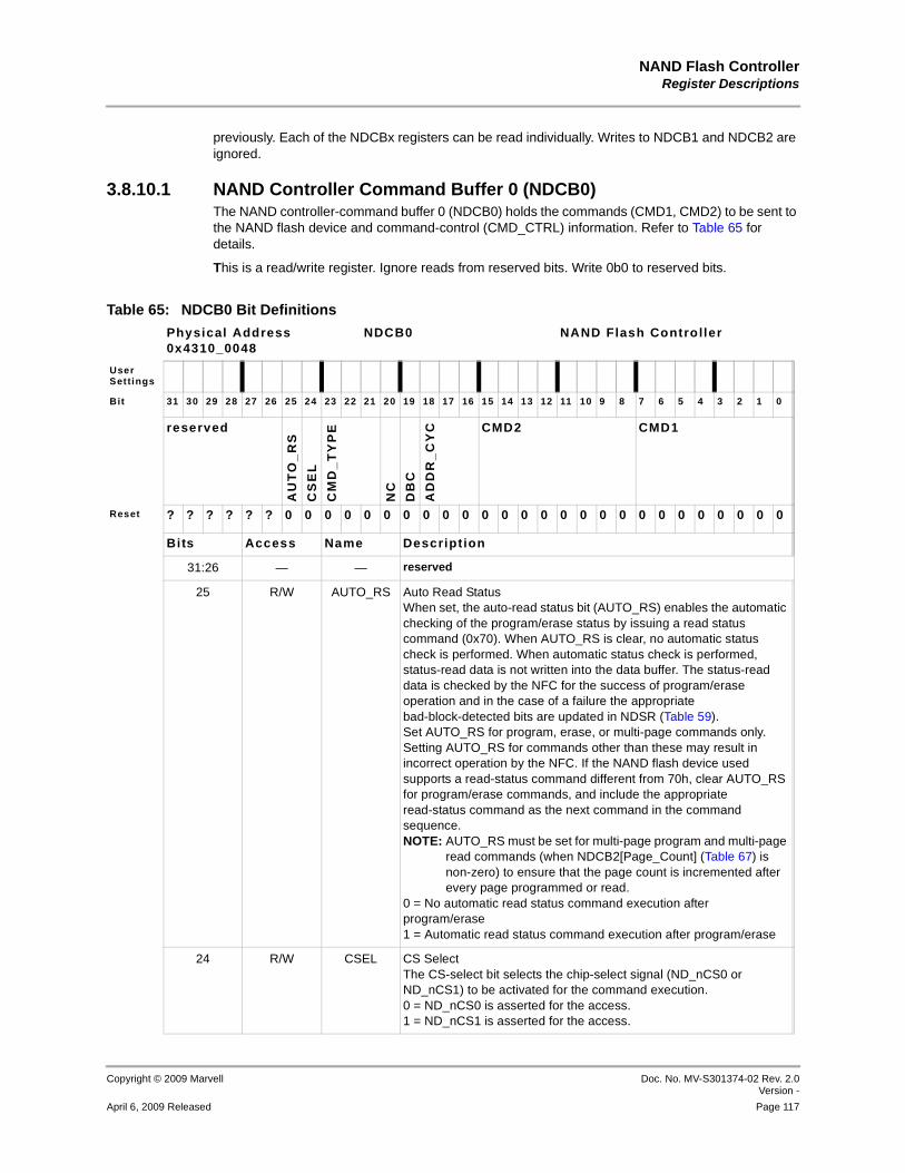
NAND Flash ControllerRegister Descriptions
Copyright © 2009 Marvell Doc. No. MV-S301374-02 Rev. 2.0Version -
April 6, 2009 Released Page 117
12345678910111213141516171819202122232425262728293031323334353637383940414243444546474849505152535455565758
previously. Each of the NDCBx registers can be read individually. Writes to NDCB1 and NDCB2 are ignored.
3.8.10.1 NAND Controller Command Buffer 0 (NDCB0)The NAND controller-command buffer 0 (NDCB0) holds the commands (CMD1, CMD2) to be sent to the NAND flash device and command-control (CMD_CTRL) information. Refer to Table 65 for details.
This is a read/write register. Ignore reads from reserved bits. Write 0b0 to reserved bits.
Table 65: NDCB0 Bit Definitions
Physical Address0x4310_0048
NDCB0 NAND Flash Controller
User Settings
Bit 31 30 29 28 27 26 25 24 23 22 21 20 19 18 17 16 15 14 13 12 11 10 9 8 7 6 5 4 3 2 1 0
reserved
AU
TO
_R
S
CS
EL
CM
D_
TY
PE
NC
DB
C
AD
DR
_C
YC CMD2 CMD1
Reset ? ? ? ? ? ? 0 0 0 0 0 0 0 0 0 0 0 0 0 0 0 0 0 0 0 0 0 0 0 0 0 0
Bits Access Name Descript ion
31:26 — — reserved
25 R/W AUTO_RS Auto Read StatusWhen set, the auto-read status bit (AUTO_RS) enables the automatic checking of the program/erase status by issuing a read status command (0x70). When AUTO_RS is clear, no automatic status check is performed. When automatic status check is performed, status-read data is not written into the data buffer. The status-read data is checked by the NFC for the success of program/erase operation and in the case of a failure the appropriate bad-block-detected bits are updated in NDSR (Table 59). Set AUTO_RS for program, erase, or multi-page commands only. Setting AUTO_RS for commands other than these may result in incorrect operation by the NFC. If the NAND flash device used supports a read-status command different from 70h, clear AUTO_RS for program/erase commands, and include the appropriate read-status command as the next command in the command sequence.NOTE: AUTO_RS must be set for multi-page program and multi-page
read commands (when NDCB2[Page_Count] (Table 67) is non-zero) to ensure that the page count is incremented after every page programmed or read.
0 = No automatic read status command execution after program/erase1 = Automatic read status command execution after program/erase
24 R/W CSEL CS SelectThe CS-select bit selects the chip-select signal (ND_nCS0 or ND_nCS1) to be activated for the command execution. 0 = ND_nCS0 is asserted for the access.1 = ND_nCS1 is asserted for the access.

PXA3xx (88AP3xx) Processor Family Vol. II: Memory Controller Configuration Developers Manual
Doc. No. MV-S301374-02 Rev. 2.0 Version -
Copyright © 2009 Marvell
Page 118 April 6, 2009 Released
12345678910111213141516171819202122232425262728293031323334353637383940414243444546474849505152535455565758
23-21 R/W CMD_TYPE Command TypeCommand type (CMD_TYPE) defines the type of NAND flash command represented by CMD1 (and CMD2 if for a double byte command). NOTE: No data transfer occurs when erase or reset commands are
executed. The NDSR bits for read-data request and write-data request (see Table 59) are not set and DMA requests are not made in DMA mode of operation when these commands are executed.
0b000 - Read0b001 - Program (Write)0b010 - Erase0b011 - Read ID0b100 - Status Read0b101 - ResetAll Other values - Reserved
20 R/W NC Next CommandThe next-command (NC) bit (if set) indicates the presence of another valid command following the current command. The NAND flash controller makes the next command DMA request if the NC bit is set. The last command of a command sequence must have the NC bit clear.0 = No valid command following the current command.1 = Valid command following the current command.
19 R/W DBC Double Byte CommandThe double-byte command (DBC) bit (if set) indicates that the current command involves the transfer of two commands to the NAND flash. DBC must be clear for a single-byte command.0 = Current command is a single-byte command.1 = Current command is a double-byte command.
Table 65: NDCB0 Bit Definitions (Continued)
Physical Address0x4310_0048
NDCB0 NAND Flash Controller
User Settings
Bit 31 30 29 28 27 26 25 24 23 22 21 20 19 18 17 16 15 14 13 12 11 10 9 8 7 6 5 4 3 2 1 0
reserved
AU
TO
_R
S
CS
EL
CM
D_
TY
PE
NC
DB
C
AD
DR
_C
YC CMD2 CMD1
Reset ? ? ? ? ? ? 0 0 0 0 0 0 0 0 0 0 0 0 0 0 0 0 0 0 0 0 0 0 0 0 0 0
Bits Access Name Descript ion

NAND Flash ControllerRegister Descriptions
Copyright © 2009 Marvell Doc. No. MV-S301374-02 Rev. 2.0Version -
April 6, 2009 Released Page 119
12345678910111213141516171819202122232425262728293031323334353637383940414243444546474849505152535455565758
3.8.10.2 NAND Controller Command Buffer 1 (NDCB1)NAND controller-command Buffer 1 (NDCB1) contains the addresses to be sent to the NAND flash in multiple cycles. In NAND-flash mode, I/O<7:0> pins are used to send ADDRx<7:0>, in as many cycles as defined by NDCB0[ADDR_CYC]. The ADDR5 field in NAND controller command Buffer 2 (NDCB2) is used to specify the fifth cycle of address for devices supporting five addressing cycles. Contents of the ADDRx fields are sent out sequentially by the NAND controller during the addressing phase. Program these fields with address values based on the cycle-by-cycle addressing specified by the NAND-flash device.
When programming an Erase command, the contents of ADDR1 must be replicated in ADDR5 to save the full address during a bad-block detect since only fields ADDR2 through ADDR5 are saved. When programming a manual Read-Status command, write the ADDRx fields with the same address as the previous command to save a valid address to NDBDRx during a bad-block detect. Refer to Table 66, “NDCB1 Bit Definitions” for more details.
This is a read-only register. Ignore reads from reserved bits.
18-16 R/W ADDR_CYC Number of Address CyclesAddress cycles (ADDR_CYC) specifies the number of address cycles in which the NAND flash is to be addressed. Valid values for address cycles are 1 to 5 for NAND commands Program, Read, Erase and Read-Id. For example, if ADDR_CYC value is programmed as 4, ADDR1, ADDR2, ADDR3, and ADDR4 (see Section 3.8.10.2) are sent to the flash device in successive address cycles, while ADDR5 is ignored (see Section 3.8.10.3).
NOTE: Valid value for address cycles for Reset and Read-status commands is 0. If the software programs a non-zero value for these commands the NAND controller ignores it.
15-8 R/W CMD2 Second commandThe second command (CMD2) contains the second byte of command sent to NAND flash after CMD1 and address in a double-byte command.NOTE: Only valid when NDCB0[DMB] is set.
7-0 R/W CMD1 First commandThe first command (CMD1) contains the first byte command sent to the NAND flash when the command execution begins.
Table 65: NDCB0 Bit Definitions (Continued)
Physical Address0x4310_0048
NDCB0 NAND Flash Controller
User Settings
Bit 31 30 29 28 27 26 25 24 23 22 21 20 19 18 17 16 15 14 13 12 11 10 9 8 7 6 5 4 3 2 1 0
reserved
AU
TO
_R
S
CS
EL
CM
D_
TY
PE
NC
DB
C
AD
DR
_C
YC CMD2 CMD1
Reset ? ? ? ? ? ? 0 0 0 0 0 0 0 0 0 0 0 0 0 0 0 0 0 0 0 0 0 0 0 0 0 0
Bits Access Name Descript ion
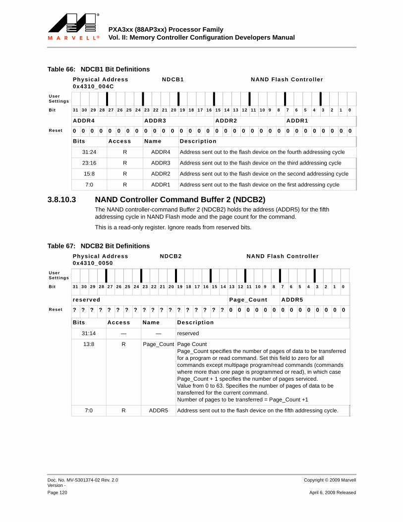
PXA3xx (88AP3xx) Processor Family Vol. II: Memory Controller Configuration Developers Manual
Doc. No. MV-S301374-02 Rev. 2.0 Version -
Copyright © 2009 Marvell
Page 120 April 6, 2009 Released
12345678910111213141516171819202122232425262728293031323334353637383940414243444546474849505152535455565758
3.8.10.3 NAND Controller Command Buffer 2 (NDCB2)The NAND controller-command Buffer 2 (NDCB2) holds the address (ADDR5) for the fifth addressing cycle in NAND Flash mode and the page count for the command.
This is a read-only register. Ignore reads from reserved bits.
Table 66: NDCB1 Bit Definitions
Physical Address0x4310_004C
NDCB1 NAND Flash Control ler
User Settings
Bit 31 30 29 28 27 26 25 24 23 22 21 20 19 18 17 16 15 14 13 12 11 10 9 8 7 6 5 4 3 2 1 0
ADDR4 ADDR3 ADDR2 ADDR1
Reset 0 0 0 0 0 0 0 0 0 0 0 0 0 0 0 0 0 0 0 0 0 0 0 0 0 0 0 0 0 0 0 0
Bits Access Name Descript ion
31:24 R ADDR4 Address sent out to the flash device on the fourth addressing cycle
23:16 R ADDR3 Address sent out to the flash device on the third addressing cycle
15:8 R ADDR2 Address sent out to the flash device on the second addressing cycle
7:0 R ADDR1 Address sent out to the flash device on the first addressing cycle
Table 67: NDCB2 Bit Definitions
Physical Address0x4310_0050
NDCB2 NAND Flash Controller
User Settings
Bit 31 30 29 28 27 26 25 24 23 22 21 20 19 18 17 16 15 14 13 12 11 10 9 8 7 6 5 4 3 2 1 0
reserved Page_Count ADDR5
Reset ? ? ? ? ? ? ? ? ? ? ? ? ? ? ? ? ? ? 0 0 0 0 0 0 0 0 0 0 0 0 0 0
Bits Access Name Descript ion
31:14 — — reserved
13:8 R Page_Count Page CountPage_Count specifies the number of pages of data to be transferred for a program or read command. Set this field to zero for all commands except multipage program/read commands (commands where more than one page is programmed or read), in which case Page_Count + 1 specifies the number of pages serviced. Value from 0 to 63. Specifies the number of pages of data to be transferred for the current command.Number of pages to be transferred = Page_Count +1
7:0 R ADDR5 Address sent out to the flash device on the fifth addressing cycle.

Internal MemoryOverview
Copyright © 2009 Marvell Doc. No. MV-S301374-02 Rev. 2.0Version -
April 6, 2009 Released Page 121
4 Internal MemoryThis chapter describes the PXA32x, PXA31x, and PXA32x processors Internal Memory Controller (IMC) and the internal memory SRAM arrays.
4.1 OverviewThis chapter describes the Internal Memory Controller (IMC), the Mini-Internal Memory Controller (MIMC), the Internal Memory SRAM Banks (IMB), and the internal Boot ROM.
The processor supports 256 Kbytes of memory-mapped SRAM. The SRAM is divided into two banks, each consisting of 128 Kbytes arrays.
The PXA32x processor supports 768 Kbytes of memory-mapped SRAM. The SRAM is divided into six banks, each consisting of 128 Kbytes arrays
The processor supports 48 Kbytes of memory-mapped ROM, which is organized as a single bank used by the Boot ROM.
The IMC interfaces the internal memory SRAM banks and the internal Boot ROM bank with the remainder of the processor via the processor switch unit. The IMC circuitry operates only in the processor S0/D0/C0 and S0/D0/C1 power modes, although data retention is possible in some low power modes, as described in Section 4.4.4, Power Management.
The MIMC interfaces the internal memory SRAM banks with the processor mini-LCD unit via a dedicated asynchronous private interface. The MIMC has special power-saving features including individual power management for each 128 Kbyte memory array. The MIMC circuitry operates mostly in the processor S0/D1/C2 power mode (Refer to Section 4.4.4.4, MIMC Power Management of SRAM Arrays).
The processor has seven power modes. Refer to Section 4.4.4, Power Management for the status of the IMC, MIMC, and the SRAM arrays during each of these power modes.
4.1.1 PXA3xx Processor DifferencesTable 68 shows the Internal Memory Controller differences among the PXA32x, PXA31x, and PXA30x processors.
4.2 FeaturesThe processor supports the following features:
Up to 768 Kbytes of on-chip SRAM arranged in six banks, with each bank consisting of 128 Kbytes arrays.48 Kbytes of on-chip Boot ROM
Table 68: PXA3xx Processors Feature Differences
Feature PXA30x PXA31x PXA32x
Maximum Internal SRAM 256 Kbytes 256 Kbytes 768 Kbytes
Mini-IMC Supported Supported Not Supported1
1. The Mini-Internal Memory Controller is used only in S0/D1/C2 and S0/D2/C2 power modes, which are not supported on the PXA32x processor.

PXA3xx (88AP3xx) Processor Family Vol. II: Memory Controller Configuration Developers Manual
Doc. No. MV-S301374-02 Rev. 2.0 Version -
Copyright © 2009 Marvell
Page 122 April 6, 2009 Released,
IMC and MIMC support for a dual-ported interface to access the two SRAM banks, which allows the IMC to accomplish “read while write” operationsIMC arbitration and completion of read-write requests to the SRAM banks are sent from a single S0/D0/C0 mode initiator—the switch interfaceIMC completion of read-only requests to the Boot ROM are sent from a single S0/D0/C0 mode initiator—the switch interfaceMIMC completion of read-only requests to SRAM banks are sent from a single S0/D1/C2 mode initiator— the mini-LCDSupport for MIMC power management for each of the SRAM arrays in S0/D1/C2 mode, with automatic power management for reduced power consumptionIMC support for byte writes to the SRAM banks.
4.3 Signal DescriptionsThe internal memory block does not have external signals.
4.4 OperationThis section describes the operation of the SRAM banks and arrays, the IMC, and the MIMC. Internal-memory interaction with power management is also discussed.
4.4.1 SRAM Bank and ArraysThe IMC and MIMC each have a dual-ported interface, with each port interfacing to a separate SRAM bank. Each of the banks, called the upper bank and the lower bank, has up to three 128 Kbytes memory array. With six banks, the total memory size is up to 768 Kbytes. The memory mapping for each 128 Kbytes array for the PXA30x and PXA31x processors are shown in Figure 9. The memory mapping for each 128 Kbytes array for the PXA32x processor is shown in Figure 10.
Figure 9: Organization and Memory Mapping of SRAM Arrays (PXA30x and PXA31x Processors)
Upper Bank Array 00x5C02_0000 to 0x5C03_FFFF
Lower Bank Array 00x5C00_0000 to 0x5C01_FFFF
Upper Bank Lower Bank
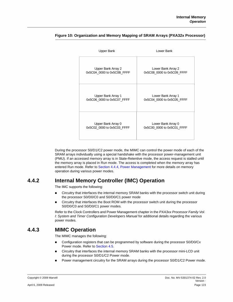
Internal MemoryOperation
Copyright © 2009 Marvell Doc. No. MV-S301374-02 Rev. 2.0Version -
April 6, 2009 Released Page 123
During the processor S0/D1/C2 power mode, the MIMC can control the power mode of each of the SRAM arrays individually using a special handshake with the processor power-management unit (PMU). If an accessed memory array is in State-Retentive mode, the access request is stalled until the memory array is placed in Run mode. The access is completed when the memory array has entered Run mode. Refer to Section 4.4.4, Power Management for more details on memory operation during various power modes.
4.4.2 Internal Memory Controller (IMC) OperationThe IMC supports the following:
Circuitry that interfaces the internal memory SRAM banks with the processor switch unit during the processor S0/D0/C0 and S0/D0/C1 power modeCircuitry that interfaces the Boot ROM with the processor switch unit during the processor S0/D0/C0 and S0/D0/C1 power modes.
Refer to the Clock Controllers and Power Management chapter in the PXA3xx Processor Family Vol. I: System and Timer Configuration Developers Manual for additional details regarding the various power modes.
4.4.3 MIMC OperationThe MIMC manages the following:
Configuration registers that can be programmed by software during the processor S0/D0/Cx Power mode. Refer to Section 4.5.Circuitry that interfaces the internal memory SRAM banks with the processor mini-LCD unit during the processor S0/D1/C2 Power mode.Power management circuitry for the SRAM arrays during the processor S0/D1/C2 Power mode.
Figure 10: Organization and Memory Mapping of SRAM Arrays (PXA32x Processor)
Upper Bank Array 20x5C0A_0000 to 0x5C0B_FFFF
Lower Bank Array 20x5C08_0000 to 0x5C09_FFFF
Upper Bank Lower Bank
Upper Bank Array 10x5C06_0000 to 0x5C07_FFFF
Lower Bank Array 10x5C04_0000 to 0x5C05_FFFF
Upper Bank Array 00x5C02_0000 to 0x5C03_FFFF
Lower Bank Array 00x5C00_0000 to 0x5C01_FFFF
PXA3xx (88AP3xx) Processor Family Vol. II: Memory Controller Configuration Developers Manual
Doc. No. MV-S301374-02 Rev. 2.0 Version -
Copyright © 2009 Marvell
Page 124 April 6, 2009 Released,
4.4.4 Power ManagementThe processor has seven power modes: S0/D0/C0, S0/D0/C1, S0/D1/C2, S0/D2/C2, and S2/D3/C4, S3/D4/C4, and S4/D4/C4. The PXA32x processor has five power modes: S0/D0/C0, S0/D0/C1, and S2/D3/C4, S3/D4/C4, and S4/D4/C4. Refer to the Clock Controllers and Power Management chapter in the PXA3xx Processor Family Vol. I: System and Timer Configuration Developers Manual for additional details regarding the various power modes.
This section describes the status of the IMC, MIMC, and the SRAM arrays during each of these power modes.
4.4.4.1 Power Management of IMC and MIMC ModulesThe IMC stays in an Active-Run mode when the processor is in S0/D0/C0 mode. The MIMC stays in an active-Run mode when the processor is in S0/D1/C2 mode.The controllers are in State-Retentive mode when the processor is in S0/D2/C2 mode and is turned off during S2/D3/C4 and S3/D4/C4 modes.
4.4.4.2 SRAM Array Power ModesThe SRAM arrays can be in one of three power modes: Run, State-Retentive, and off.
1. Run mode: Represents the normal powered-up mode during which the arrays can be accessed immediately.
2. Off mode: Represents a non-State-Retentive mode during which the arrays memory cell internal states are lost.
3. State-retentive mode: Represents a State-retentive low-power mode.
4.4.4.3 IMC Power Management of SRAM ArraysThe IMC accesses the SRAM arrays during S0/D0/C0 mode only and the targeted SRAM array is in Run mode only. Unlike the MIMC, the IMC does not perform any power management. The IMC only acknowledges transactions initiated by the switch without requesting any power mode changes (for the SRAM arrays) to the processor power manager.
A Write request by the switch interface is acknowledged by the IMC, regardless of the targeted-array power mode.
4.4.4.4 MIMC Power Management of SRAM ArraysThe MIMC accesses the SRAM arrays only during S0/D1/C2 mode. During this time, the processor power mode and the SRAM arrays are in one of three power modes: Off, Run, or State Retentive.
If the mini-LCD unit initiates a Read to an array in Run mode, the MIMC does not request the processor power manager for any power-mode changes. The MIMC instead immediately initiates the mini-LCD access to the targeted array.
If the mini-LCD unit initiates a Read to an array in State-Retentive mode, the arrays are not accessed immediately. Instead, the MIMC requests that the processor power management unit place the accessed array in Run mode. The Read transaction is completed only after the power manager changes the targeted array to Run mode.
Memory arrays that are in State-Retentive mode can be moved into Run mode by the MIMC in one of the following two ways:
If a memory array in State-Retentive mode is accessed when in S0/D1/C2 mode, the internal-memory power manager requests that the processor power-management unit place the accessed array in Run mode. The memory access is held in a pending state and allowed to go

Internal MemoryOperation
Copyright © 2009 Marvell Doc. No. MV-S301374-02 Rev. 2.0Version -
April 6, 2009 Released Page 125
through only after the array power mode is changed. The internal memory block ignores a new transaction request while one is pending.If an access is initiated to an address within 512 bytes of the starting address of the memory array and the memory array is programmed for automatic wake up, the internal-memory power manager requests that the processor power-management unit place the array in Run mode.
If a memory array has not been accessed for a programmable amount of time, the MIMC requests that the power-management unit place that memory array in State-Retentive mode. This feature reduces the power consumption of that array. The programmed time is set using IMPMCR[DDT]. Refer to Section 4.5.2, IM Power Management Control Register (IMPMCR) for more details.
Figure 11 illustrates the power mode changes that are requested by the MIMC to the power management unit during S0/D1/C2 mode.
Figure 11: Power Mode Changes Initiated by Internal Memory Controller
Figure 12: Power Mode Changes Initiated by Mini-Internal Memory Controller
RunMode
Time Since Last Access > DDT
Reset
Access Requested To Current Array-OR-
Previous Array Address < 512State-retentive Mode
RunMode
Time Since Last Access > DDT
Reset
Access Requested To Array
State-retentive Mode
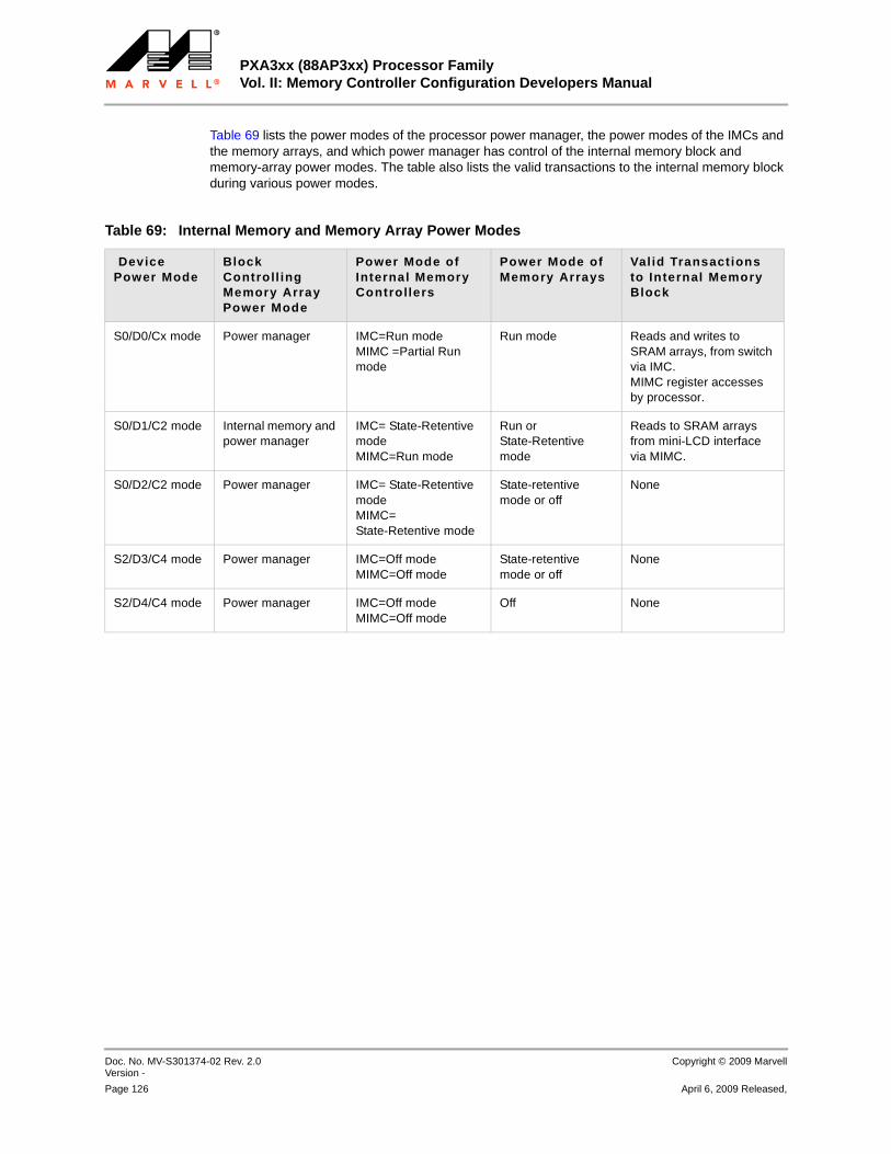
PXA3xx (88AP3xx) Processor Family Vol. II: Memory Controller Configuration Developers Manual
Doc. No. MV-S301374-02 Rev. 2.0 Version -
Copyright © 2009 Marvell
Page 126 April 6, 2009 Released,
Table 69 lists the power modes of the processor power manager, the power modes of the IMCs and the memory arrays, and which power manager has control of the internal memory block and memory-array power modes. The table also lists the valid transactions to the internal memory block during various power modes.
Table 69: Internal Memory and Memory Array Power Modes
Device Power Mode
Block Controll ing Memory Array Power Mode
Power Mode of Internal Memory Controllers
Power Mode of Memory Arrays
Valid Transactions to Internal Memory Block
S0/D0/Cx mode Power manager IMC=Run modeMIMC =Partial Run mode
Run mode Reads and writes to SRAM arrays, from switch via IMC.MIMC register accesses by processor.
S0/D1/C2 mode Internal memory and power manager
IMC= State-Retentive modeMIMC=Run mode
Run or State-Retentive mode
Reads to SRAM arrays from mini-LCD interface via MIMC.
S0/D2/C2 mode Power manager IMC= State-Retentive modeMIMC= State-Retentive mode
State-retentive mode or off
None
S2/D3/C4 mode Power manager IMC=Off modeMIMC=Off mode
State-retentive mode or off
None
S2/D4/C4 mode Power manager IMC=Off modeMIMC=Off mode
Off None
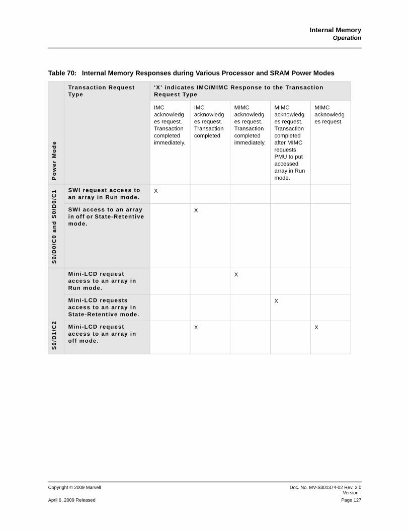
Internal MemoryOperation
Copyright © 2009 Marvell Doc. No. MV-S301374-02 Rev. 2.0Version -
April 6, 2009 Released Page 127
Table 70: Internal Memory Responses during Various Processor and SRAM Power Modes
Po
we
r M
od
e
Transaction Request Type
‘X’ indicates IMC/MIMC Response to the Transact ion Request Type
IMC acknowledges request.Transaction completed immediately.
IMC acknowledges request.Transaction completed
MIMC acknowledges request.Transaction completed immediately.
MIMC acknowledges request.Transaction completed after MIMC requests PMU to put accessed array in Run mode.
MIMC acknowledges request.
S0
/D0
/C0
an
d S
0/D
0/C
1 SWI request access to an array in Run mode.
X
SWI access to an array in off or State-Retentive mode.
X
S0
/D1
/C2
M ini-LCD request access to an array in Run mode.
X
Mini-LCD requests access to an array in State-Retentive mode.
X
Mini-LCD request access to an array in off mode.
X X

PXA3xx (88AP3xx) Processor Family Vol. II: Memory Controller Configuration Developers Manual
Doc. No. MV-S301374-02 Rev. 2.0 Version -
Copyright © 2009 Marvell
Page 128 April 6, 2009 Released,
Refer to Section 4.4.4, Power Management for more details regarding the internal memory power-management operation.
4.5 Register DescriptionsThe IMC has only one register.
4.5.1 Register SummaryTable 71 lists the register associated with the Internal Memory controller and the physical address used to access it.
S0
/D2
/C2
, S
2/D
3/C
4 a
nd
S3
/D4
/C4 Transactions to the
internal memory are functional ly impossible
The IMC and MIMC are powered down and do not respond to any transaction requests. The SRAM arrays are also powered down and not accessed.
Table 70: Internal Memory Responses during Various Processor and SRAM Power Modes P
ow
er
Mo
de
Transaction Request Type
‘X’ indicates IMC/MIMC Response to the Transact ion Request Type
IMC acknowledges request.Transaction completed immediately.
IMC acknowledges request.Transaction completed
MIMC acknowledges request.Transaction completed immediately.
MIMC acknowledges request.Transaction completed after MIMC requests PMU to put accessed array in Run mode.
MIMC acknowledges request.
Table 71: Register Internal Memory Address Map
Physical Address
Name Descript ion
0x5800_0000 IMPMCR IM Power Management Control register
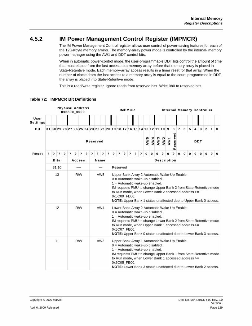
Internal MemoryRegister Descriptions
Copyright © 2009 Marvell Doc. No. MV-S301374-02 Rev. 2.0Version -
April 6, 2009 Released Page 129
4.5.2 IM Power Management Control Register (IMPMCR)The IM Power Management Control register allows user control of power-saving features for each of the 128-Kbyte memory arrays. The memory-array power mode is controlled by the internal- memory power manager using the AW1 and DDT control bits.
When in automatic power-control mode, the user-programmable DDT bits control the amount of time that must elapse from the last access to a memory array before that memory array is placed in State-Retentive mode. Each memory-array access results in a timer reset for that array. When the number of clocks from the last access to a memory array is equal to the count programmed in DDT, the array is placed into State-Retentive mode.
This is a read/write register. Ignore reads from reserved bits. Write 0b0 to reserved bits.
Table 72: IMPMCR Bit Definitions
Physical Address0x5800_0000 IMPMCR Internal Memory Controller
UserSettings
Bit 31 30 29 28 27 26 25 24 23 22 21 20 19 18 17 16 15 14 13 12 11 10 9 8 7 6 5 4 3 2 1 0
Reserved
AW
5
AW
4
AW
3
AW
2
AW
1
Re
se
rve
d
DDT
Reset ? ? ? ? ? ? ? ? ? ? ? ? ? ? ? ? ? ? 0 0 0 0 0 ? 0 0 0 0 0 0 0 0
Bits Access Name Descript ion
31:10 —- — Reserved
13 R/W AW5 Upper Bank Array 2 Automatic Wake-Up Enable:0 = Automatic wake-up disabled.1 = Automatic wake-up enabled. IM requests PMU to change Upper Bank 2 from State-Retentive mode to Run mode, when Lower Bank 2 accessed address >= 0x5C09_FE00.NOTE: Upper Bank 1 status unaffected due to Upper Bank 0 access.
12 R/W AW4 Lower Bank Array 2 Automatic Wake-Up Enable:0 = Automatic wake-up disabled.1 = Automatic wake-up enabled. IM requests PMU to change Lower Bank 2 from State-Retentive mode to Run mode, when Upper Bank 1 accessed address >= 0x5C07_FE00.NOTE: Upper Bank 0 status unaffected due to Lower Bank 3 access.
11 R/W AW3 Upper Bank Array 1 Automatic Wake-Up Enable:0 = Automatic wake-up disabled.1 = Automatic wake-up enabled. IM requests PMU to change Upper Bank 1 from State-Retentive mode to Run mode, when Lower Bank 1 accessed address >= 0x5C05_FE00.NOTE: Lower Bank 3 status unaffected due to Lower Bank 2 access.

PXA3xx (88AP3xx) Processor Family Vol. II: Memory Controller Configuration Developers Manual
Doc. No. MV-S301374-02 Rev. 2.0 Version -
Copyright © 2009 Marvell
Page 130 April 6, 2009 Released,
10 R/W AW2 Lower Bank Array 1 Automatic Wake-Up Enable:0 = Automatic wake-up disabled.1 = Automatic wake-up enabled. IM requests PMU to change Lower Bank 1 from State-Retentive mode to Run mode, when Upper Bank 0 accessed address >= 0x5C03_FE00.NOTE: Lower Bank 2 status unaffected due to Lower Bank 1 access.
9 R/W AW1 Upper Bank Array 0 Automatic Wake-Up Enable:0 = Automatic wake-up disabled.1 = Automatic wake-up enabled. IM requests PMU to change Upper Bank 0 from State-Retentive mode to Run mode,
8 — — Reserved
7:0 R/W DDT Delay State-retentive Time:Controls the amount of maximum time (in ms) with no accesses that must elapse before a memory array is placed into State-Retentive mode. If set to 0x00, State-Retentive mode is never entered.
A user-programmed value here is the maximum time in ms that elapses before the memory array is put into state-retentive. The delay time can be programmed between 1 and 255 ms. The minimum time is the (programmed value -1) ms. So, if the user programs a value of 2, the memory array is put into state-retentive between 1 and 2 ms after the last access. NOTE: Programing a value of 1 into the DDT counter places the array
into State-Retentive mode immediately after an access.
Table 72: IMPMCR Bit Definitions (Continued)
Physical Address0x5800_0000
IMPMCR Internal Memory Controller
UserSettings
Bit 31 30 29 28 27 26 25 24 23 22 21 20 19 18 17 16 15 14 13 12 11 10 9 8 7 6 5 4 3 2 1 0
Reserved
AW
5
AW
4
AW
3
AW
2
AW
1
Re
se
rve
d
DDT
Reset ? ? ? ? ? ? ? ? ? ? ? ? ? ? ? ? ? ? 0 0 0 0 0 ? 0 0 0 0 0 0 0 0
Bits Access Name Descript ion
MultiMediaCard/SD/SDIO ControllerFeatures
Copyright © 2009 Marvell Doc. No. MV-S301038-02 Rev. 2.0Version -
April 6, 2009 Released Page 131
12345678910111213141516171819202122232425262728293031323334353637383940414243444546474849505152535455565758
5 MultiMediaCard/SD/SDIO ControllerThe MultiMediaCard (MMC) and Secure Digital (SD/SDIO) controller (MMC/SD/SDIO controller) provides a software-accessible hardware link between the processor and the MMC stack (a set of memory cards). The MMC/SD/SDIO controller supports Multimedia Card, Secure Digital, and Secure Digital I/O communication protocols. The PXA30x processor contains two independent MMC/SD/SDIO controllers, and the PXA31x processor has three independent MMC/SD/SDIO controllers.
The MMC module manages the MMC system, which is a low-cost data storage and communications system.1 The MMC module is based on the standards outlined in the MultiMediaCard System Specification Version 3.3.1. The SD module manages one SD or SDIO card based on the standards outlined in the SD Memory Card Specification Version 1.10 and SDIO Card Specification Version 1.0.
The MMC/SD/SDIO controller manages the translation protocol from a standard MMC bus or from a serial peripheral interface (SPI) bus to the MMC stack. Software must select either the MMC/SD/SDIO mode or SPI mode to establish the communication protocol for the MMC/SD/SDIO controller.
5.1 FeaturesEach MMC/SD/SDIO controller has the following features:
A response FIFO (MMC_RES)Two transmit FIFOs (MMC_TXFIFO1 and MMC_TXFIFO2)
Two receive FIFOs (MMC_RXFIFO1 and MMC_RXFIFO2)Two operating modes:
• MMC/SD/SDIO mode for MMC, SD, and SDIO communication protocols.
• SPI mode for the SPI communications protocol.
One-bit and 4-bit data transfers for MMC, SD, and SDIO communication protocolsData transfer clock up to 26 MHzBased on FIFO status, turn clock on and off to prevent overflows and under-runs
Support for all valid MMC and SD/SDIO protocol data-transfer modesInterrupt-based application interface to control software interactionStream data transfers of 10 bytes or more
Multiple MMC cards for the MMC communications protocolOnly one SD or SDIO port can be used for SD or SDIO communications protocol at one time.Up to two MMC or SD/SDIO cards when the SPI communications protocol is used. Mixed card types are supported only by the SPI communications protocol per controller.Dual voltage MMC or SD/SDIO cards. For information on voltage levels, refer to the PXA30x Processor and PXA31x Processor Electrical, Mechanical, and Thermal Specification (EMTS)
1. For a detailed description of the MMC system, visit the MMC Association’s web site at www.mmca.org.

PXA3xx (88AP3xx) Processor Family Vol. II: Memory Controller Configuration Developers Manual
Doc. No. MV-S301038-02 Rev. 2.0 Version -
Copyright © 2009 Marvell
Page 132 April 6, 2009 Released
12345678910111213141516171819202122232425262728293031323334353637383940414243444546474849505152535455565758
5.2 SignalsThe MMC/SD/SDIO controller signals are described in Table 73. All signals are alternate functions on separate GPIO pins. For more information on these alternate functions and GPIO pins, refer to the Pin Descriptions and Control, and the General Purpose I/O Unit (GPIO) chapters in the PXA30x Processor and PXA31x Processor Vol. I: System and Timer Configuration Developer’s Manual.
5.3 OperationThe MMC/SD/SDIO controller:
Provides all card-specific functions.
Serves as the bus master for the MMC system.Implements the standard interface to the card stack.Provides card initialization.
Provides CRC generation and validation.Handles command, response, and data transactions.
The MMC/SD/SDIO controller is a slave to software. The controller consists of command and control registers, a response FIFO, and data FIFOs. The software has access to these registers and FIFOs, and it generates commands, interprets responses, and controls subsequent actions.
Table 73: Multimedia Card and Secure Digital I/O Signal Summary
Signal Pin
Mode Direct ion Descript ion
MMCLK MMC and SD/SDIO
Output Bus clock
SPI Output SPI clock
MMCMD MMC and SD/SDIO
Output Bidirectional Signal for command and responses
SPI Output Output for command and write data
MMDAT0 MMC and SD/SDIO
Bidirectional Read and write data
SPI Input Input for response token and read data
MMDAT1 MMC and SD/SDIO Bidirectional
Read and write data for 4-bit data transfers
SPI Input Signals an interrupt condition to the controller
MMDAT2MMCCS0
MMC and SD/SDIO
Bidirectional Read and write data for 4-bit data transfers
SPI Output CS0 chip select
MMDAT3MMCCS1
MMC and SD/SDIO
Bidirectional Read and write data for 4-bit data transfers
SPI Output CS1 chip select
MultiMediaCard/SD/SDIO ControllerOperation
Copyright © 2009 Marvell Doc. No. MV-S301038-02 Rev. 2.0Version -
April 6, 2009 Released Page 133
12345678910111213141516171819202122232425262728293031323334353637383940414243444546474849505152535455565758
For the MMC system, the MMCMD pin must be pulled up external to the MMC controller. There can be an incorrect CRC response generation in the MMC controller if the MMCMD pin is not pulled up, Refer to Section 5.5.3 for details.
The card stack and the controller communicate serially through the command and data lines and implement a message-based protocol. The messages consist of the following tokens:
Command. A six-byte token that starts an operation. The command set includes card initialization, card register Reads and Writes, and data transfers. The MMC/SD/SDIO controller sends the command serially on the MMCMD pin. Table 74 shows the format for a command.
Response. A token that is an answer to a command token. Each command has either a specific response type or no response type. The format for a response varies according to the command sent and the card mode. Data. Is transferred serially between the MMC/SD/SDIO controller and the card in eight-bit blocks and at rates up to 26 MHz. The format for the data depends on the card mode. Table 75 shows the data format for MMC/SD/SDIO mode.
In MMC/SD/SDIO mode, all operations contain a command and most commands have an associated response. Read and write commands also have data transfers. Command and response are sent and received on the bidirectional MMCMD signal, and data is sent and received on the bidirectional MMDAT signal. Figure 13 shows a typical MMC/SD/SDIO mode command timing diagram with and without a response. Figure 14 shows a typical MMC/SD/SDIO mode timing diagram for a sequential read or write.
Table 74: Command Format
Bit Posit ion
47 46 [45:40] [39:8] [7:1] 0
Width (bits) 1 1 6 32 7 1
Value 0 1 x x x 1
Description start bit transmission bit command index
argument CRC7 end bit
Table 75: MMC/SD/SDIO Data Token Format
Stream Data 1 x no CRC 1
Block Data 0 x x 1
Descript ion start bit data CRC7 end bit

PXA3xx (88AP3xx) Processor Family Vol. II: Memory Controller Configuration Developers Manual
Doc. No. MV-S301038-02 Rev. 2.0 Version -
Copyright © 2009 Marvell
Page 134 April 6, 2009 Released
12345678910111213141516171819202122232425262728293031323334353637383940414243444546474849505152535455565758
Not all commands are available in SPI mode. The available commands have both a command and response. The MMCMD and MMDAT signals are not bidirectional in SPI mode. The MMCMD is an output pin and the MMDAT is an input pin with respect to the processor. The command and data to be written are sent on the MMCMD signal, and the response and read data is received on the MMDAT signal. Figure 15 shows a typical SPI mode timing diagram without a data token. Figure 16 and Figure 17 show SPI mode read and write timing diagrams, respectively.
Figure 13: MMC/SD/SDIO Mode Operation Without Data Transfer
Figure 14: MMC/SD/SDIO Mode Operation With Data Transfer
Figure 15: SPI Mode Operation Without Data Transfer
CommandMMCMD
MMDAT
Operation (No Response) Operation (No Data)
Command Response
From Host to Card(s) From Card to Host
From Host to Card
CommandMMCMD
MMDAT
Data Transfer Operation Data Stop Operation
Response
Data Stream
From Host to Card(s)
From Card to Host Stop Command
Stops Data Transfer
Command Response
Data to/from Card and Host
CommandMMCMD
MMDAT
Command
Response
From Host to Card From Card to HostFrom Host to Card
Response Busy
From Card to Host

MultiMediaCard/SD/SDIO ControllerOperation
Copyright © 2009 Marvell Doc. No. MV-S301038-02 Rev. 2.0Version -
April 6, 2009 Released Page 135
12345678910111213141516171819202122232425262728293031323334353637383940414243444546474849505152535455565758
The MMC/SD/SDIO controller can interface to the cards with the MMC protocol, SD/SDIO protocol, or SPI protocol. All protocols are serial interfaces to the cards as shown in Table 76. The MMC protocol is for block, multiple-block, and stream-data transfers. The SD/SDIO protocol is for block and multiple-block data transfers. The SPI protocol is for block and multiple-block data transfers.
Note
Note For MMC data stream transfers of 10 or more bytes are supported only.
Figure 16: SPI Mode Read Operation
Figure 17: SPI Mode Write Operation
CommandMMCMD
MMDAT
Command
Response
From Host to Card Data from Card to Host Next Command
Data Block CRC
From Card to Host
CommandMMCMD
MMDAT
Command
Response
From Host to Card Data from Host to CardNew Command from Host
Data Response Busy
From Card to
Data Block
Data Response and Busy from Card
Table 76: MMC/SD/SDIO Data Transfer Types
Data TransferTypes MMC Protocol SD and SDIO Protocol SPI Protocol
Single block Yes Yes Yes
Multiple block - open-ended Yes Yes Yes
Multiple block - predefined Yes Yes Yes
Stream Yes No No
RW_IO Direct, CMD52 No for SDIO only for SDIO only
RW_IO Extended, CMD53 No for SDIO only for SDIO only
PXA3xx (88AP3xx) Processor Family Vol. II: Memory Controller Configuration Developers Manual
Doc. No. MV-S301038-02 Rev. 2.0 Version -
Copyright © 2009 Marvell
Page 136 April 6, 2009 Released
12345678910111213141516171819202122232425262728293031323334353637383940414243444546474849505152535455565758
5.3.1 MMC/SD/SDIO ModeIn the MMC/SD/SDIO mode, MMCMD and MMDATx are bidirectional and require external pullup resistors. The command and response are sent on MMCMD. Multiple-byte data is sent on MMDAT0.
In the MMC protocol, card addressing occurs during the initialization phase with address assignment. A card is then addressed by an address in the command argument. In the SD/SDIO protocol, card addressing is implemented by point-to-point MMCMD and MMDATx signals. The command is protected with a suffixed 7-bit CRC. The response length is 48 or 136 bits, and it can be protected with a suffixed 7-bit CRC, depending on the response type.
A read or write-data transfer is protected with a suffixed 16-bit CRC. In write-data transfers, after the data and the16-bit CRC have been transmitted, the card sends a 5-bit CRC status token, which indicates whether the data transmission was erroneous. After the CRC status token, the card may indicate that it is busy programming the data by pulling the DAT0 pin low.
5.3.2 MMC/SD/SDIO Data Transfer ModesThe MMC/SD/SDIO mode manages these data-transfer modes:
Single block read/writeMultiple block read/write
• Open-ended multiple block read/write
• Multiple block-read/write with predefined block count
Stream read/write (MMC Only)
An application can stop all data transfers at any time with an MMC/SD stop-transmission command (CMD12) or an SDIO abort command (with CMD52 and ASx bits set). Cards must not respond to CMD12 unless they are in the data, rcv, or irq states. Therefore, if no response is received for a CMD12, it is reasonable to send a status query such as CMD13, which is valid for all memory card states in data transfer mode, to determine the card state before proceeding to error handling.
5.3.2.1 Single-Block Data Transfers A single block of data is transmitted in single block-data transfers. The starting address is specified along with the read/write command. The application must provide the block size with the number of bytes to transfer to the controller. The data block is protected with a 16-bit CRC that is generated by the transmit unit and is checked by the receive unit. The CRC is appended after transfer of the last data bit.
5.3.2.2 Multiple-Block Data TransfersMultiple block-data transfers are similar to the single block-data transfers, except multiple blocks of data are transferred sequentially. Each block is the same length. Each block is stored to or retrieved from contiguous-memory addresses, starting at the address specified in the command.
Two types of multiple block-data transfers are defined:
Open-ended multiple block-read/write. The number of blocks to be transferred is not defined in the card. The card continuously transfers data blocks until it receives a stop-transmission command (CMD12).
Multiple-block read/write with predefined block count. The number of blocks to be transferred is defined in the card, which transfers only the number of data blocks specified. A stop-transmission command (CMD12) or abort command (CMD52 with ASx bits set) is not required at the end of the data transfer (in this case) unless the data transmission terminates with an error. To start a multiple block-data transmission with a predefined block count, a SET_BLOCK_COUNT command (CMD16) must immediately precede the multiple block command (CMD18/CMD25). The application must provide the block size and the number of blocks to transfer to the controller. Each data block is protected with a 16-bit CRC.
MultiMediaCard/SD/SDIO ControllerOperation
Copyright © 2009 Marvell Doc. No. MV-S301038-02 Rev. 2.0Version -
April 6, 2009 Released Page 137
12345678910111213141516171819202122232425262728293031323334353637383940414243444546474849505152535455565758
The card stops data transmission if the card detects an error during a multiple block-read operation of either type. The application must then stop the transmission with the stop- transmission command (CMD12). If the card detects an error during a multiple block-write operation of either type, the card ignores any additional incoming data. The application must then stop the transmission with the stop-transmission command (CMD12).
The application can stop a data transmission at any time. An MMC/SD stop-transmission command (CMD12) or an SDIO abort command (with CMD52 with ASx bits set) terminates multiple-block data transfers, regardless of the type. Neither CMD12 or CMD52 is needed to stop transmission at the end of a pre-defined multiple block-data transfer.
5.3.2.3 Stream Data Transfers (MMC Only)The MMC controller transmits a continuous stream of data for stream data transfers. The starting address is specified in the read/write command. The data stream is terminated with a stop-transmission command (CMD12). For write transfers, CMD12 must be aligned with the last six bytes of data to ensure that no more and no less data is written to the card. For read transfers, CMD12 can occur after the data has been transmitted. There is no CRC protection on the data when using stream-data transfers.
Only data sizes of 10 bytes or more are allowed for stream data transfers.
5.3.2.4 SPI ModeSPI mode is an optional secondary communication protocol. In SPI mode, the MMCMD and MMDAT0 pins are unidirectional:
MMCMD is an output from the controller, and it sends the command and write data to the MMC/SD/SDIO card. MMDAT0 is an input to the controller, and it receives the response and read data from the MMC/SD/SDIO card.
Note
Note When the card is in SPI mode, the only way to return to MMC/SD/SDIO mode is to toggle the power to the card.
Card addressing is implemented with hardware chip selects, MMCCS1 and MMCCS0. All command, response, data tokens, and data are eight bits long and are byte aligned to the assertion of the respective chip select.
The command is protected with a suffixed 7-bit CRC. The card always sends a response to a command. The response has several formats, including an 8-bit error response. The length of the response is one, two, or five bytes. SPI mode offers a non-protected mode. In this mode, CRC bits of the command and data tokens are still suffixed to the command and data tokens, but the card and the controller ignore these bits.
For write-data transfers from the controller, the card responds with an 8-bit CRC status token. As in MMC/SD/SDIO mode, the card can indicate that it is busy by pulling MMDAT0 low after the CRC status token. In read-data transfers, the card can respond with the data or a one-byte data-error token.
5.3.3 MMC ModeIn MMC mode, the bidirectional MMCMD and MMDAT signals require external pullup resistors. Command and response are sent and received through MMCMD; data is read and written through MMDAT. After an MMC card is powered on, it is assigned a default relative-card address (RCA) of 0x0001. Software assigns different addresses to each card during the initialization sequence
PXA3xx (88AP3xx) Processor Family Vol. II: Memory Controller Configuration Developers Manual
Doc. No. MV-S301038-02 Rev. 2.0 Version -
Copyright © 2009 Marvell
Page 138 April 6, 2009 Released
12345678910111213141516171819202122232425262728293031323334353637383940414243444546474849505152535455565758
described in Section 5.5.2. A card is then addressed by its new RCA, which is sent in that argument portion of the command that is protected with a suffixed 7-bit CRC (see Table 74).
The response has several formats, including a no-response. The response length is 48 bits or 136 bits, and can be protected with a suffixed 7-bit CRC.
For write-data transfers from the controller, the card responds with a 5-bit CRC status token. After sending the CRC status token, the card can indicate that it is busy by pulling MMDAT0 low.
The start address for a read operation can be any random byte address in the valid address space of the card memory. For a write operation, the start address must be on a sector boundary and the data length must be an integer multiple of the sector length. A sector is the number of blocks that are erased during the write operation (before data is written), and it is fixed for each MMC card. A block is the number of bytes to be transferred.
5.4 SD/SDIO ModeSDIO cards are based on and are compatible with SD cards. The SDIO card provides high-speed data I/O with low-power consumption for mobile electronic devices. Features of SDIO include:
Plug-and-play (PnP)
Multi-function, including multiple I/O and combined I/O and memoryUp to seven I/O functions plus one memory on one cardAllows cards to interrupt application
Read_Wait operationSuspend/Resume operation
5.4.1 New I/O Read/Write CommandsSDIO includes two new data transfer commands, as follows:
IO_RW_DIRECT Command (CMD52). Allows the simplest access to a single register within the 128K register space in any I/O function. The command is similar to the MMC fast-I/O command (CMD39). For SDIO, CMD52 also replaces the MMC/SD stop-transmission command (CMD12). CMD52 can be used to abort a data transfer by writing to the SDIO card CCCR Abort register. IO_RW_EXTENDED Command (CMD53). Allows the read/write of multiple I/O registers with a single command. I/O block operations use CMD53 rather than MMC/SD memory-block read/write commands. CMD53 supports multi-byte transfer modes and block mode, which are analogous to MMC/SD single and multiple block-data transfers. Multi-byte mode Reads or Writes multiple bytes of data to/from a single I/O register. Block mode Reads or Writes multiple bytes of data to/from an I/O register address that is incremented by 1 after each operation/block. In SDIO, CMD53 is similar to the following MMC/SD commands for memory data transfer.In multi-byte mode:
• READ_SINGLE_BLOCK (CMD17)
• WRITE_SINGLE_BLOCK (CMD24)
In block mode:
• READ_MULTIPLE_BLOCK (CMD18)
• WRITE_MULTIPLE_BLOCK (CMD25)
Multi-byte or block mode is specified in the command argument. In the block mode, the number of blocks to be transferred is specified in the command argument. Therefore, the application does not need to stop the data transmission, as in MMC/SD multiple block-data transfers, because the number of blocks of data transferred is known by the card and the MMC/SD/SDIO controller. In multi-byte mode, if the byte/block count field in the CMD53 argument is 0, 512

MultiMediaCard/SD/SDIO ControllerSD/SDIO Mode
Copyright © 2009 Marvell Doc. No. MV-S301038-02 Rev. 2.0Version -
April 6, 2009 Released Page 139
12345678910111213141516171819202122232425262728293031323334353637383940414243444546474849505152535455565758
bytes are read or written. Also, the MMC_BLKLEN register should be written with the value of 512.
If the byte/block count field in the CMD53 argument is 0 in block mode, the data transfer is identical to the memory mode open-ended multiple block-data transfer and more than 511 blocks are to be transferred. In this case, the data transmission must be aborted by writing the I/O abort function bits.
5.4.2 SD Switch FunctionThe SD switch function command, CMD6, switches or expands SD memory card functions. CMD6 can switch between 1-bit and 4-bit mode when preceded by CMD55. CMD6 has an R1 response and the SD card transmits 512 bits on the DAT lines. Therefore, CMD6 looks like a standard single-block read data transfer of 512 bits. The host must wait a minimum of 8 clocks after the end bit of the data before using the new functions.
5.4.3 SDIO Data Transfer AbortsThe application can issue an I/O abort any time during an I/O extended read or write data transfer by writing a CMD52 to the SDIO card CCCR register. The abort stops the data transmission. On data Writes, the abort occurs between data blocks. Also, after an I/O card receives an abort on a data write, the card can respond as busy after sending the CMD52 response.
5.4.4 SDIO InterruptsAn SDIO card can generate an interrupt request to the CPU by driving MMDAT1 low. The card continues to keep MMDAT1 low until the CPU recognizes and acts on the interrupt request or the interrupt request is de-asserted due to the end of the SDIO interrupt period.
5.4.5 SDIO Suspend/ResumeFor SDIO, the application can temporarily halt (suspend) a data transfer to one function or to memory to free the SDIO bus for a higher-priority data transfer to a different function or memory. After the higher-priority data transfer completes, the application can resume the suspended data transfer from the point where it halted.
Note
Note The application can suspend multiple transactions and resume them in any preferred order. The suspend/resume operation works for SD/SDIO 1-bit and 4-bit modes. It does not apply to SPI mode.
5.4.6 SDIO Read WaitFor MMC and SD cards, the controller prevents an MMC_RXFIFO overrun by stopping the clock during a read data transfer. The controller restarts the clock and continues the data transfer when the MMC_RXFIFO is ready for more data. Stopping the clock is a limitation for SDIO because a CMD52 cannot be issued while the clock is stopped.
SDIO uses a read-wait (RD_WAIT) operation to enable the host to send a CMD52. With read-wait, the host uses MMDAT2 to signal the card temporarily to stop sending read data. This signal allows a CMD52 to be sent while the data is halted.
When the application requests a RD_WAIT to be sent from the controller to the card, the data transfer may not halt immediately. Therefore, the READ_WAIT request from the controller does not
PXA3xx (88AP3xx) Processor Family Vol. II: Memory Controller Configuration Developers Manual
Doc. No. MV-S301038-02 Rev. 2.0 Version -
Copyright © 2009 Marvell
Page 140 April 6, 2009 Released
12345678910111213141516171819202122232425262728293031323334353637383940414243444546474849505152535455565758
stop the MMC_RXFIFOs from turning the clock off/on to prevent overflows. The application must continue to read the MMC_RXFIFOs during the RD_WAIT operation.
The RD_WAIT operation is supported only for multiple-block read-data transfers in SDIO 1-bit and 4-bit modes.It is not supported in SPI mode.
5.4.7 SDIO InterruptsAn SDIO card can implement an interrupt condition to the controller. If the MMC_CMDAT[SDIO_INT_EN] bit is set, the controller monitors and reports any interrupt conditions from the card. If an interrupt condition occurs, the MMC_STAT[SDIO_INT] bit is set and an interrupt request is generated if the mask bit is set in the MMC_I_MASK register.
5.4.8 SDIO Suspend/ResumeThe SDIO suspend/resume operation suspends a data transfer to an SDIO function or to memory to free the bus for a higher-priority data transfer to a different function or memory. After the higher-priority data transfer completes, the original data transfer can resume.
For multiple-block data transfers, the suspend operation suspends any data transfer between blocks even if it has not been started on the bus.
Software can suspend any data transfer by specifying CMD52 during the data transfer. The argument of CMD52 must be set to suspend the current function. The MMC_CMDAT[SDIO_SUSPEND] bit must be set. When the card acknowledges the suspend operation, the MMC_STAT[SDIO_SUSPEND_ACK] bit is set and the MMC_I_REG register is asserted. The number of suspended blocks is written into the MMC_BLKS_REM register. Software must read and save the MMC_BLKS_REM register value for use when the data transfer resumes.
For SDIO suspend/resume operations (CMD52), the data programmed into the MMC_CMDAT register must be set for the command that is to be suspended or resumed, not the actual CMD52 itself (bits 2 and 3 are the bits that are commonly set incorrect). The MMC/SDIO controller does not store the context of the command being suspended or resumed, so the appropriate bits must always be set even when suspending or resuming current transactions.
The data transfer can complete before the card acknowledges the suspend operation. In this case, the DATA_TRAN_DONE bit is set.
For multiple-block Writes or a CMD53 block-mode write, the controller does not send any data to the card if the data transfer is not started when the SDIO_SUSPEND bit is set. If a data transfer is in progress when the SDIO_SUSPEND bit is set, the controller stops sending data to the card after the current data block is completed. The number of blocks that are not transferred is recorded in the MMC_BLKS_REM register.
Software can resume any suspended data transfer by specifying CMD52. The command argument must be set to resume the function and the MMC_CMDAT[SDIO_RESUME] bit must be set. Also, the MMC_NUMBLK must be written with the number of blocks in MMC_BLKS_REM when the data transfer is suspended. If DMA descriptors are used to read from or write to the FIFOs, software must stop the DMA channel when the SDIO_SUSPEND_ACK bit is set.
5.4.9 SDIO Read WaitThe SDIO READ_WAIT operation allows software to stall a data transfer temporarily. This operation is supported only for SDIO multiple-block read data transfers.
If READ_WAIT is specified, the controller drives the DAT2 pin low at the end of a data block to signal the card to enter its READ_WAIT state. During the READ_WAIT time, software can specify CMD52 to communicate with any other SDIO card function. Software can restart the stalled read-data transfer at any time.

MultiMediaCard/SD/SDIO ControllerMMC/SD/SDIO Controller Functional Description
Copyright © 2009 Marvell Doc. No. MV-S301038-02 Rev. 2.0Version -
April 6, 2009 Released Page 141
12345678910111213141516171819202122232425262728293031323334353637383940414243444546474849505152535455565758
Software uses MMC_RDWAIT register to control the READ_WAIT operation. The MMC_RDWAIT[RD_WAIT_EN] bit enables the controller to drive the DAT2 pin low at the end of a data block and therefore stall the data transfer from the card. Software writes to the MMC_RDWAIT[RD_WAIT_START] bit to enable the controller to restart the stalled data transfer.
When a data transfer is stalled, the MMC_STAT[RD_STALLED] bit is asserted and the RD_STALLED interrupt request is generated if the appropriate mask bit is set.
Software must continue reading MMC_RXFIFO to prevent the FIFO from turning MMCLK off. Therefore, software must monitor the RD_STALLED interrupt condition in parallel with reading the MMC_RXFIFO.
5.5 MMC/SD/SDIO Controller Functional DescriptionSoftware must read and write the MMC/SD/SDIO controller registers and FIFOs to initiate communication to a card. The controller provides the interface between software and the MMC/SD/SDIO bus. It is responsible for the timing and protocol between software and the MMC/SD/SDIO bus. The controller consists of:
Control and status registersOne 16-bit response FIFO that is eight entries deepTwo 8-bit MMC_RXFIFOs that are each 32 entries deep
Two 8-bit MMC_TXFIFOs that are each 32 entries deep
The registers and FIFOs are accessible to software. The MMC/SD/SDIO controller also enables minimal data latency by buffering data and generating and checking CRCs. Refer to Section 5.3 for examples.
5.5.1 ResetThe MMC/SD/SDIO controller is reset by processor reset only. All registers and FIFO controls are set to their default values after any reset. For more information on resets, refer to the Services Power Management Chapter in the PXA30x Processor and PXA31x Processor Vol. I: System and Timer Configuration Developer’s Manual.
5.5.2 Card Initialization SequenceAfter reset, the MMC/SD/SDIO controller sends 80 clocks on MMCLK to initialize the MMC card, and software sets the MMC_CMDAT[INIT] bit to 0b1 to initialize the MMC card. Consequently, 80 clocks are sent before the current command in the MMC_CMD register is sent. This procedure is useful for acquiring new cards inserted onto the bus. In SPI mode, chip selects are not asserted during the initialization sequence.
After the 80-clock initialization sequence, software must send CMD1 continuously by loading the appropriate command index into the MMC_CMD register until the card indicates that the power-up sequence is complete. Software can then assign an address to the card or place it into SPI mode.
5.5.3 Response and Data Error DetectionThe MMC/SD/SDIO controller detects response and data errors on the MMC/SD/SDIO bus and reports them in the MMC_STAT status register. Response errors are also recorded in the RES_ERR interrupt bit. Data errors are also recorded in the DAT_ERR interrupt bit. If a response or data error occurs, the bit is set in the MASK and an interrupt request is generated to the interrupt controller if the appropriate mask bit is cleared. Software can either respond to an interrupt request or poll the MMC_I_REG.
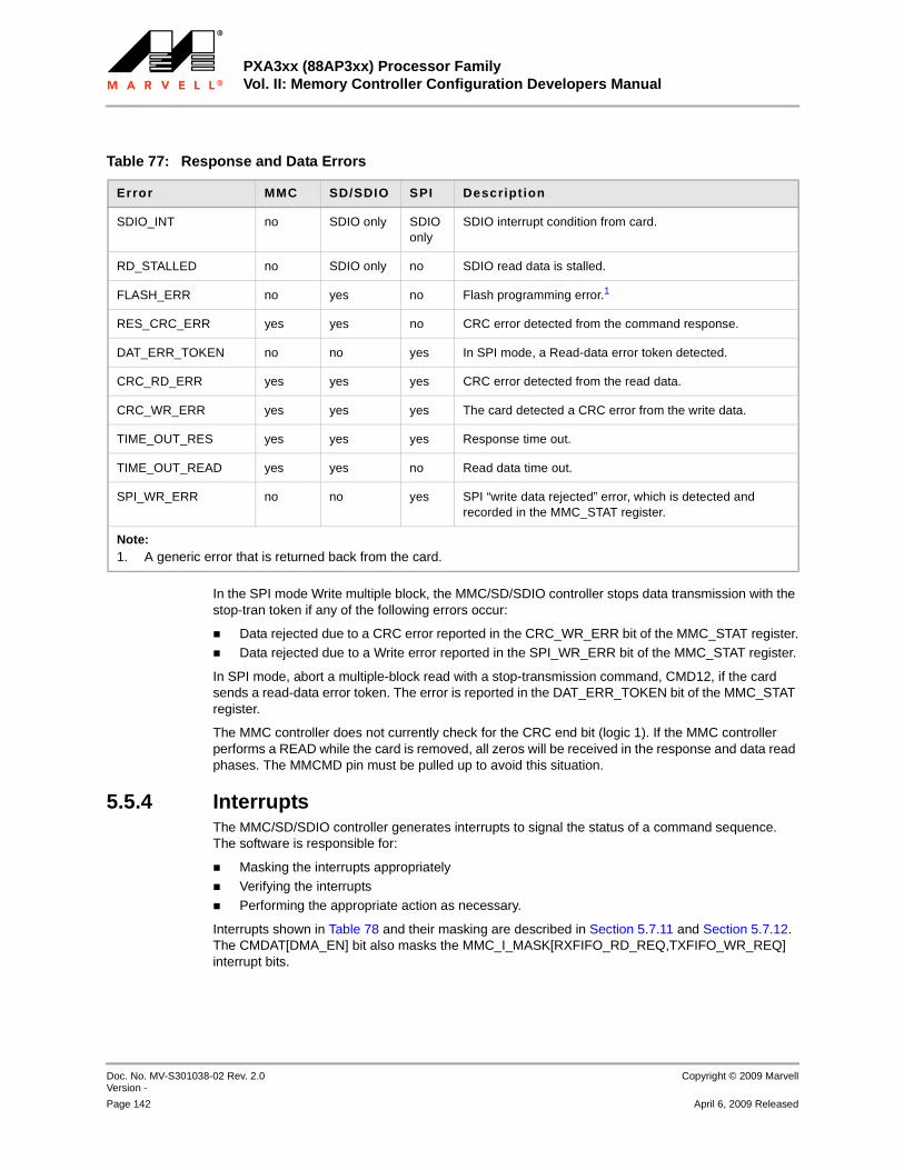
PXA3xx (88AP3xx) Processor Family Vol. II: Memory Controller Configuration Developers Manual
Doc. No. MV-S301038-02 Rev. 2.0 Version -
Copyright © 2009 Marvell
Page 142 April 6, 2009 Released
12345678910111213141516171819202122232425262728293031323334353637383940414243444546474849505152535455565758
In the SPI mode Write multiple block, the MMC/SD/SDIO controller stops data transmission with the stop-tran token if any of the following errors occur:
Data rejected due to a CRC error reported in the CRC_WR_ERR bit of the MMC_STAT register.Data rejected due to a Write error reported in the SPI_WR_ERR bit of the MMC_STAT register.
In SPI mode, abort a multiple-block read with a stop-transmission command, CMD12, if the card sends a read-data error token. The error is reported in the DAT_ERR_TOKEN bit of the MMC_STAT register.
The MMC controller does not currently check for the CRC end bit (logic 1). If the MMC controller performs a READ while the card is removed, all zeros will be received in the response and data read phases. The MMCMD pin must be pulled up to avoid this situation.
5.5.4 InterruptsThe MMC/SD/SDIO controller generates interrupts to signal the status of a command sequence. The software is responsible for:
Masking the interrupts appropriatelyVerifying the interruptsPerforming the appropriate action as necessary.
Interrupts shown in Table 78 and their masking are described in Section 5.7.11 and Section 5.7.12. The CMDAT[DMA_EN] bit also masks the MMC_I_MASK[RXFIFO_RD_REQ,TXFIFO_WR_REQ] interrupt bits.
Table 77: Response and Data Errors
Error MMC SD/SDIO SPI Descript ion
SDIO_INT no SDIO only SDIO only
SDIO interrupt condition from card.
RD_STALLED no SDIO only no SDIO read data is stalled.
FLASH_ERR no yes no Flash programming error.1
RES_CRC_ERR yes yes no CRC error detected from the command response.
DAT_ERR_TOKEN no no yes In SPI mode, a Read-data error token detected.
CRC_RD_ERR yes yes yes CRC error detected from the read data.
CRC_WR_ERR yes yes yes The card detected a CRC error from the write data.
TIME_OUT_RES yes yes yes Response time out.
TIME_OUT_READ yes yes no Read data time out.
SPI_WR_ERR no no yes SPI “write data rejected” error, which is detected and recorded in the MMC_STAT register.
Note:1. A generic error that is returned back from the card.
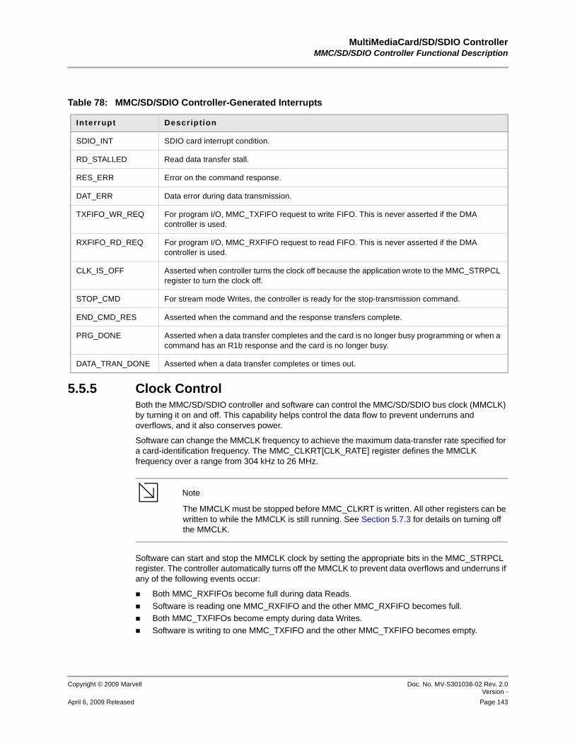
MultiMediaCard/SD/SDIO ControllerMMC/SD/SDIO Controller Functional Description
Copyright © 2009 Marvell Doc. No. MV-S301038-02 Rev. 2.0Version -
April 6, 2009 Released Page 143
12345678910111213141516171819202122232425262728293031323334353637383940414243444546474849505152535455565758
5.5.5 Clock ControlBoth the MMC/SD/SDIO controller and software can control the MMC/SD/SDIO bus clock (MMCLK) by turning it on and off. This capability helps control the data flow to prevent underruns and overflows, and it also conserves power.
Software can change the MMCLK frequency to achieve the maximum data-transfer rate specified for a card-identification frequency. The MMC_CLKRT[CLK_RATE] register defines the MMCLK frequency over a range from 304 kHz to 26 MHz.
Note
Note The MMCLK must be stopped before MMC_CLKRT is written. All other registers can be written to while the MMCLK is still running. See Section 5.7.3 for details on turning off the MMCLK.
Software can start and stop the MMCLK clock by setting the appropriate bits in the MMC_STRPCL register. The controller automatically turns off the MMCLK to prevent data overflows and underruns if any of the following events occur:
Both MMC_RXFIFOs become full during data Reads.
Software is reading one MMC_RXFIFO and the other MMC_RXFIFO becomes full.Both MMC_TXFIFOs become empty during data Writes.Software is writing to one MMC_TXFIFO and the other MMC_TXFIFO becomes empty.
Table 78: MMC/SD/SDIO Controller-Generated Interrupts
Interrupt Description
SDIO_INT SDIO card interrupt condition.
RD_STALLED Read data transfer stall.
RES_ERR Error on the command response.
DAT_ERR Data error during data transmission.
TXFIFO_WR_REQ For program I/O, MMC_TXFIFO request to write FIFO. This is never asserted if the DMA controller is used.
RXFIFO_RD_REQ For program I/O, MMC_RXFIFO request to read FIFO. This is never asserted if the DMA controller is used.
CLK_IS_OFF Asserted when controller turns the clock off because the application wrote to the MMC_STRPCL register to turn the clock off.
STOP_CMD For stream mode Writes, the controller is ready for the stop-transmission command.
END_CMD_RES Asserted when the command and the response transfers complete.
PRG_DONE Asserted when a data transfer completes and the card is no longer busy programming or when a command has an R1b response and the card is no longer busy.
DATA_TRAN_DONE Asserted when a data transfer completes or times out.

PXA3xx (88AP3xx) Processor Family Vol. II: Memory Controller Configuration Developers Manual
Doc. No. MV-S301038-02 Rev. 2.0 Version -
Copyright © 2009 Marvell
Page 144 April 6, 2009 Released
12345678910111213141516171819202122232425262728293031323334353637383940414243444546474849505152535455565758
For Read data transfers, the controller turns on MMCLK after the MMC_RXFIFO is emptied. For Write data transfers, the controller turns on MMCLK after the MMC_TXFIFO is no longer empty.
If software stops MMCLK at any time, it must wait for either the MMC_STAT[CLK_EN] status bit to be cleared or the CLK_IS_OFF interrupt request before proceeding.
When the 26 MHz bit clock input is used and the bit clock is started through MMC_STRPCL[STRT_CLK], MMC_STRPCL[STOP_CLK] can still stop the bit clock for at least two bit clocks.
5.5.6 Data FIFOsThe controller FIFOs for response, received data, and transmitted data are MMC_RES, MMC_RXFIFO, and MMC_TXFIFO, respectively. These FIFOs are accessible to software and are described in the following paragraphs.
5.5.6.1 Response Data FIFO (MMC_RES)The response FIFO (MMC_RES) contains the response received from an MMC/SD/SDIO card after the controller sends a command. The response FIFO is read only, 16 bits wide, and 8 entries deep. It holds all possible response lengths. Responses that are only one byte long are located on the LSBs of the 16-bit entry in the response FIFO. For Reads of odd byte length responses, the last byte is located on the LSBs of the 16-bit entry in the response FIFO.
The response FIFO does not contain the response CRC. The status of the CRC check is shown by the MMC_STAT[RES_CRC_ERR] bit.
5.5.6.2 Receive Data FIFO (MMC_RXFIFO)The two MMC_RXFIFOs are read-only and are readable on 1-, 2-, or 4- byte boundaries. Each MMC_RXFIFO is 32 entries deep and 1 byte wide. Access to the MMC_RXFIFOs is handled by the controller and depends on the status of the MMC_RXFIFOs.
Both MMC_RXFIFOs and their controls are cleared to a starting state after a system reset and at the beginning of all command sequences, except for the stop-transmission command (CMD12) or the IO_RW_DIRECT command (CMD52).
The MMC_RXFIFOs swap between software and MMC/SD/SDIO bus. At any time, while software has read access to one of the MMC_RXFIFOs, the MMC/SD/SDIO bus has Write access to the other MMC_RXFIFO. For example, the MMC_RXFIFOs are called MMC_RXFIFO1 and MMC_RXFIFO2. After a reset or at the beginning of a command sequence, both MMC_RXFIFOs are empty and software has read access to MMC_RXFIFO1 while the MMC/SD/SDIO bus has Write access to MMC_RXFIFO2. When MMC_RXFIFO2 becomes full and MMC_RXFIFO1 is empty, the MMC_RXFIFOs swap and software now has read access to MMC_RXFIFO2 and the MMC/SD/SDIO bus now has Write access to MMC_RXFIFO1. When MMC_RXFIFO1 becomes full and MMC_RXFIFO2 is empty, the MMC_RXFIFOs swap again and software now has read access to MMC_RXFIFO1 and the MMC/SD/SDIO bus now has Write access to MMC_RXFIFO2. This swapping process continues throughout the data transfer and is transparent to both software and the MMCMMC/SD/SDIO controller.
If at any time both MMC_RXFIFOs become full and the data transmission is not complete, the controller turns off MMCLK to prevent any overflows. When MMCLK is off, data transmission from the card stops until MMCLK is turned on again. After software empties the MMC_RXFIFO to which it is connected, the controller turns on MMCLK to continue data transmission.
5.5.6.3 Transmit Data FIFO (MMC_TXFIFO)The two MMC_TXFIFOs are written only by software and are writable on a 1-, 2-, or 4-byte boundary. Each MMC_TXFIFO is 32 entries deep and 1 byte wide. Access to the FIFOs is handled by the controller and depends on the status of the FIFOs.
MultiMediaCard/SD/SDIO ControllerMMC/SD/SDIO Card Communication Protocol
Copyright © 2009 Marvell Doc. No. MV-S301038-02 Rev. 2.0Version -
April 6, 2009 Released Page 145
12345678910111213141516171819202122232425262728293031323334353637383940414243444546474849505152535455565758
Both MMC_TXFIFOs and their controls are cleared to a starting state after a system reset and at the beginning of all command sequences, except for the stop-transmission command (CMD12) or the IO_RW_Direct command (CMD52).
The FIFOs swap between the software and the MMC bus. At any time while software has Write access to one of the FIFOs, the MMC bus has Read access to the other FIFO, and vice versa. For example, the FIFOs are called MMC_TXFIFO1 and MMC_TXFIFO2. After a reset or at the beginning of a command sequence, both FIFOs are empty and software has Write access to MMC_TXFIFO1 while the MMC/SD/SDIO bus has read access to MMC_TXFIFO2. When MMC_TXFIFO1 becomes full and MMC_TXFIFO2 is empty, the FIFOs swap and the software now has Write access to MMC_TXFIFO2 and the MMC/SD/SDIO bus now has read access to MMC_TXFIFO1. When MMC_TXFIFO2 becomes full and MMC_TXFIFO1 is empty, the FIFOs swap again and software now has Write access to MMC_TXFIFO1 and the MMC/SD/SDIO bus now has read access to MMC_TXFIFO2. This swapping process continues throughout the data transfer and is transparent to both software and the MMC/SD/SDIO controller.
If at any time both MMC_TXFIFOs become empty and the data transmission is not complete, the controller turns off MMCLK to prevent any underruns. When MMCLK is off, data transmission to the card stops until MMCLK is turned on again. When the FIFOs are no longer empty, the MMC/SD/SDIO controller automatically restarts MMCLKk.
If the software does not fill the MMC_TXFIFO to which it is connected, software must set the MMC_PRTBUF[PRT_BUF] bit to an 0b1, which enables the MMC_TXFIFOs to swap without first being filled.
5.5.7 DMA and Program I/OSoftware communicates with the MMC/SD/SDIO controller through DMA or programmed I/O.
To access the MMC/SD/SDIO controller FIFOs by DMA, software must program the DMA channel to read or write the FIFOs with 1-byte transfers and 32-byte bursts. For example, to write 64 bytes of data to a MMC_TXFIFO, software must program the DMA channel to write 64 bytes with an 8-bit port size to the MMC/SD/SDIO controller using 32-byte bursts. The controller issues a request to read a MMC_RXFIFO and a request to write a MMC_TXFIFO.
With programmed I/O, software waits for MMC_I_REG[MMC_RXFIFO_RD_REQ] or MMC_I_REG[MMC_TXFIFO_WR_REQ] to generate interrupt requests, if enabled, before reading or writing the respective FIFO. Alternatively, the application can poll the MMC_I_REG register for the FIFO request by disabling the interrupt in the interrupt controller or by setting the appropriate mask bits. A maximum of 32 bytes can be read/written for each interrupt condition.
The CMDAT[DMA_EN] bit must be set to enable communication with DMA and it must be cleared to enable communication with programmed I/O.
5.6 MMC/SD/SDIO Card Communication ProtocolThis section discusses software responsibilities and the communication protocols that are used between the MMC/SD/SDIO controller and the card.
5.6.1 Start and Stop ClockSoftware stops the clock as follows:
1. Ensure the MMC_I_REG[CLK_IS_OFF] interrupt is not masked by clearing the MMC_I_MASK[CLK_IS_OFF]
2. Set MMC_STRPCL[STOP_CLK] to stop MMCLK.3. Wait for the MMC_I_REG[CLK_IS_OFF] interrupt request.
To restart MMCLK, software must set the MMC_STRPCL[STRT_CLK].
PXA3xx (88AP3xx) Processor Family Vol. II: Memory Controller Configuration Developers Manual
Doc. No. MV-S301038-02 Rev. 2.0 Version -
Copyright © 2009 Marvell
Page 146 April 6, 2009 Released
12345678910111213141516171819202122232425262728293031323334353637383940414243444546474849505152535455565758
5.6.2 Enabling SPI ModeTo communicate with a card in SPI mode, software must write the MMC_SPI register as follows:
1. Set the MMC_SPI[SPI_CS_ADDRESS] bit to enable the card connected to the MMCS1 pin. 2. Clear the MMC_SPI[SPI_CS_ADDRESS] bit to enable the card connected to the MMCS0 pin.3. Set MMC_SPI[SPI_CS_EN].to enable the SPI chip select.
4. Set MMC_SPI[SPI_CRC_EN] to enable protected SPI mode. Clear MMC_SPI[SPI_CRC_EN] to enable SPI non-protected mode.
5. Set MMC_SPI[SPI_MODE].to enable SPI mode.
Note
Note When the card is in SPI mode, the only way to return to MMC/SD/SDIO mode is to toggle power to the card.
5.6.3 MMC Card Stream Data Write (MMC Only)A stream-data Write performs like the single-block Write except that a stop-transmission command (CMD12) is sent in parallel with the last six bytes of data. After writing the MMC_CMDAT register, software must start the process of filling the MMC_TXFIFO as described in Section 5.6.7. Then it proceeds as follows:
1. Wait for the MMC_I_REG[STOP_CMD] interrupt request. This interrupt request indicates that the MMC/SD/SDIO controller is ready for the stop-transmission command (CMD12).
2. Write the registers for a stop-transmission command. 3. Wait for the MMC_I_REG[DATA_TRAN_DONE] interrupt request and
MMC_I_REG[PRG_DONE] interrupt request.
These bits must be programmed in MMC_CMDAT for a data Write:
Set SD_4DAT to enable 4-bit mode
Set DMA_EN to enable DMASet STRM_BLK to enable Stream modeSet MMC_CMDATWR_RD to enable Write data transfers
DATA_EN
Also, the following registers must be configured appropriately:
MMC_BLKLEN[BLK_LEN] must be configured with the number of bytes to be transferred.MMC_NUMBLK[NUM_BLK] must be set to 0x0001.
Note
Note Before the transfer is initiated, MMC_BLKLEN must be programmed with the number of bytes to be written. This is different than the MMC specification requirements for a stream data Write operation, which can be stopped with CMD12 at any time before the maximum number of bytes are transferred.
MultiMediaCard/SD/SDIO ControllerMMC/SD/SDIO Card Communication Protocol
Copyright © 2009 Marvell Doc. No. MV-S301038-02 Rev. 2.0Version -
April 6, 2009 Released Page 147
12345678910111213141516171819202122232425262728293031323334353637383940414243444546474849505152535455565758
5.6.4 MMC Card Stream Data Read (MMC Only)The stream data read looks like the single-block Read except that a stop-transmission command (CMD12) must be sent after the data transfer. After writing the MMC_CMDAT register, software must start the process of reading the MMC_RXFIFO as described in Section 5.6.12.2.
When it uses DMA, software must also configure the DMA channel to send an interrupt request after all the data is read. After the DMA interrupt request, or after software reads all of the data, software must send the stop-transmission command (CMD12).
These bits must be specified in MMC_CMDAT for a data read:
SD_4DAT for 4-bit modeDMA_EN for the DMA
STRM_BLK must be setClear WR_RD for a ReadDATA_EN
Also, the following registers must be configured appropriately:
MMC_BLKLEN to specify the number of bytes to transfer.MMC_NUMBLK must be configured to 0x0001
MMC_RDTO to specify the read time-out period
Note
Note Before the transfer is initiated, MMC_BLKLEN must be programmed with the number of bytes to be read. This is different than the MMC specification requirements for stream data-Read operation, which can be stopped with CMD12 any time before the max number of bytes are transferred.
5.6.5 Basic, No Data, Command and Response SequenceThe MMC/SD/SDIO controller performs basic MMC/SD or SPI bus transactions. It formats the command from the command registers and generates and appends a 7-bit CRC, if applicable. It then performs the following steps:
1. Serially transmits the result on MMCMD. 2. Collects the response data.
3. Validates the response CRC.
It also checks for response time-outs and card-busy, if applicable. The response data is placed into the MMC_RES FIFO and the status of the transaction is recorded in the MMC_STAT status register. Software accomplishes these tasks by writing the Control registers as follows:
1. Write to the following registers, as necessary:
• MMC_CMD
• MMC_ARGH
• MMC_ARGL
• MMC_RESTO
2. Write to MMC_CMDAT with the appropriate value. This register must always be written, even if there is no change to the register. Writing MMC_CMDAT starts the command sequence.
PXA3xx (88AP3xx) Processor Family Vol. II: Memory Controller Configuration Developers Manual
Doc. No. MV-S301038-02 Rev. 2.0 Version -
Copyright © 2009 Marvell
Page 148 April 6, 2009 Released
12345678910111213141516171819202122232425262728293031323334353637383940414243444546474849505152535455565758
3. Write to the MMC_I_MASK register, and wait for and verify the MMC_I_REG[END_CMD_RES] interrupt condition or poll the MMC_STAT or MMC_I_REG registers for END_CMD_RES.
4. Read the MMC_RES FIFO and MMC_STAT registers.
Some cards may become busy as the result of receiving a command. Software can wait for the card to become not busy by writing to the MMC_I_MASK register and waiting for the MMC_I_REG[PRG_DONE] interrupt condition. Alternatively, software can start communication with another card. Software cannot access the same card again until the card is no longer busy. For details, refer to MultiMediaCard System Specification Version 3.3.1.
5.6.6 Card Data TransferA data transfer is a command and response sequence with the addition of a data transfer to/from a card. Software must follow the steps presented in the preceding section (Section 5.6.5). Before writing the MMC_CMDAT register, software must write the following registers as necessary.
MMC_RDTOMMC_BLKLENMMC_NUMBLK
Next, software must read MMC_RES and read or write the MMC_RXFIFOs or MMC_TXFIFOs. After completely reading or writing the data FIFOs, software must wait for the appropriate interrupt requests or poll. The MMC_STAT status register must be read to check the status of the transaction and ensure that the transaction is complete.
When using DMA requests, the controller indicates to the DMA controller when a FIFO is ready for reading or writing. All FIFO Reads and Writes should empty and fill the FIFO to which they are connected. If at any time software does not fill the MMC_TXFIFO (32 bytes), software must notify the controller by setting the MMC_PRTBUF[PRT_BUF]. Software can write more bytes of data than is needed into the MMC_TXFIFO, but the controller transmits only the number of bytes specified in the MMC_BLKLEN register.
During write-data transfers, a card can become busy while programming the data. Software can wait for the card to become not busy by writing the MMC_I_MASK register and waiting for the MMC_I_REG[PRG_DONE] interrupt request. Alternatively, software can start communication with another card. For details, refer to the MultiMediaCard System Specification Version 3.3.1.
The MMC/SD/SDIO controller performs data transactions in all the basic modes: Single Block, Multiple Blocks, and Stream.
5.6.7 Card Block Data WriteA block of data is written to a card in a single-block data Write. In a multiple-block Write, the controller performs multiple single-block write-data transfers on the MMC/SD/SDIO bus.
If both MMC_TXFIFOs become empty during data transmission, the MMC/SD/SDIO controller turns off MMCLK. After a MMC_TXFIFO is written, the controller turns on MMCLK.
These bits must be programmed in MMC_CMDAT for a data Write:
SD_4DAT for 4-bit modeDMA_EN for the DMA
STRM_BLK if the data transfer type is in Stream mode (MMC Only)WR_RD for a WriteDATA_EN
Also, the following registers must be configured appropriately:
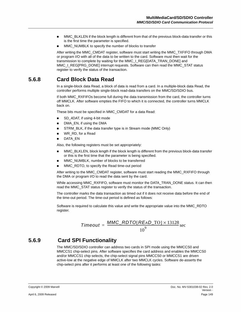
MultiMediaCard/SD/SDIO ControllerMMC/SD/SDIO Card Communication Protocol
Copyright © 2009 Marvell Doc. No. MV-S301038-02 Rev. 2.0Version -
April 6, 2009 Released Page 149
12345678910111213141516171819202122232425262728293031323334353637383940414243444546474849505152535455565758
MMC_BLKLEN if the block length is different from that of the previous block-data transfer or this is the first time the parameter is specified.MMC_NUMBLK to specify the number of blocks to transfer
After writing the MMC_CMDAT register, software must start writing the MMC_TXFIFO through DMA or program I/O with all of the data to be written to the card. Software must then wait for the transmission to complete by waiting for the MMC_I_REG[DATA_TRAN_DONE] and MMC_I_REG[PRG_DONE] interrupt requests. Software can then read the MMC_STAT status register to verify the status of the transaction.
5.6.8 Card Block Data ReadIn a single-block data Read, a block of data is read from a card. In a multiple-block data Read, the controller performs multiple single-block read-data transfers on the MMC/SD/SDIO bus.
If both MMC_RXFIFOs become full during the data transmission from the card, the controller turns off MMCLK. After software empties the FIFO to which it is connected, the controller turns MMCLK back on.
These bits must be specified in MMC_CMDAT for a data Read:
SD_4DAT, if using 4-bit modeDMA_EN, if using the DMA
STRM_BLK, if the data transfer type is in Stream mode (MMC Only)WR_RD, for a ReadDATA_EN
Also, the following registers must be set appropriately:
MMC_BLKLEN, block length if the block length is different from the previous block-data transfer or this is the first time that the parameter is being specified.MMC_NUMBLK, number of blocks to be transferredMMC_RDTO, to specify the Read time-out period
After writing to the MMC_CMDAT register, software must start reading the MMC_RXFIFO through the DMA or program I/O to read the data sent by the card.
While accessing MMC_RXFIFO, software must monitor the DATA_TRAN_DONE status. It can then read the MMC_STAT status register to verify the status of the transaction.
The controller marks the data transaction as timed out if it does not receive data before the end of the time-out period. The time-out period is defined as follows:
Software is required to calculate this value and write the appropriate value into the MMC_RDTO register.
5.6.9 Card SPI FunctionalityThe MMC/SD/SDIO controller can address two cards in SPI mode using the MMCCS0 and MMCCS1 chip-select pins. After software specifies the card address and enables the MMCCS0 and/or MMCCS1 chip selects, the chip-select signal pins MMCCS0 or MMCCS1 are driven active-low at the negative edge of MMCLK after two MMCLK cycles. Software de-asserts the chip-select pins after it performs at least one of the following tasks:
Timeout MMC_RDTO READ_TO[ ] 13128×10
9------------------------------------------------------------------------------------------- sec=
PXA3xx (88AP3xx) Processor Family Vol. II: Memory Controller Configuration Developers Manual
Doc. No. MV-S301038-02 Rev. 2.0 Version -
Copyright © 2009 Marvell
Page 150 April 6, 2009 Released
12345678910111213141516171819202122232425262728293031323334353637383940414243444546474849505152535455565758
Turn off the chip-select enable.Select a different card.
Software specifies the card address in the MMC_SPI register. The address can be changed for every command.
In SPI mode, software can perform a CRC check. The default is no CRC checking. The command and data are sent on the MMC/SD/SDIO bus aligned to every eight MMCLKs as described in the SPI section of the MultiMediaCard System Specification Version 3.3.1.
In a Read sequence, the card can return data or a data-error token. If a data-error token is received, the controller stops the transmission and updates the status register.
In a system with multiple cards running in SPI mode, there is a limitation if the system must interleave commands to both cards. For example, when programming Card 0, then switch to Card 1, then back to Card 0, the Status register bits do not properly reflect the status of the active card. The workaround is to program the GPIO so that it monitors the SPI interface of interest. Poll the GPIO status register to obtain the status of either card.
5.6.10 SDIO Card Communication ProtocolSDIO cards can perform data transfers in 1-bit or 4-bit mode. Software selects 1-bit or 4-bit data transfers by writing to the SD_4DAT bit in the MMC_CMDAT register.
5.6.11 Basic, No Data, Command-Response SequenceThe MMC/SD/SDIO controller performs the basic MMC/SD/SDIO transaction as follows:
1. Format the command from the MMC_CMD, CMD_ARGH and CMD_ARGL Command registers.
2. Generate and append the 7-bit CRC, if applicable.3. Serially transmit the command and CRC to the MMC/SD/SDIO CMD bus.
The MMC/SD/SDIO controller then collects the response data, validates the CRC, and checks for response time-outs and the card busy condition, if applicable. The response data is located in the MMC_RES FIFO, and the transaction status is located in the MMC_STAT Status register. To accomplish these tasks, the application completes the following steps:
1. Write to the Control registers, as necessary.2. Write to the MMC_CMDAT register.
3. Either poll MMC_STAT[END_CMD_RES] or unmask MMC_I_MASK[END_CMD_RES] and wait for the END_CMD_RES interrupt request from the controller.
4. Read the command response from the MMC_RES FIFO.5. Wait for PRG_DONE by polling or interrupt request if the command is expected to respond
busy.6. Check the status in MMC_STAT Status register.
The command sequence starts on the MMC/SD/SDIO bus after software writes to the MMC_CMDAT register. Some cards can become busy as the result of a command. The application can wait for the card to become “not busy” by any of the following methods:
Write to the MMC_I_MASK register and wait for the PRG_DONE interrupt request.Poll the MMC_STATUS register.
Start communicating with another card.
Software cannot access the same card again until the card is no longer busy.

MultiMediaCard/SD/SDIO ControllerMMC/SD/SDIO Card Communication Protocol
Copyright © 2009 Marvell Doc. No. MV-S301038-02 Rev. 2.0Version -
April 6, 2009 Released Page 151
12345678910111213141516171819202122232425262728293031323334353637383940414243444546474849505152535455565758
5.6.12 Data TransferA data transfer is a command-response sequence with the addition of a data transfer to/from a card. For details, refer to the examples in Section 5.6.
Software must execute the protocol described in Section 5.6.11. After software writes the registers, it must complete the following steps:
1. Begin the read or write of the MMC_RXFIFO or MMC_TXFIFO, respectively.
2. Wait for END_CMD_RES.3. Read the MMC_RES as described in the basic, no data, command-response sequence in
Section 5.6.11.
After software reads or writes the data FIFOs, it must wait for the appropriate interrupt requests to ensure that the transaction is complete and then check the transaction status in the MMC_STAT status register.
Using request signals, the controller indicates to software when a FIFO is ready for Reads or Writes. All application FIFO Reads/Writes empty/fill the FIFO to which they are connected. If at any time the MMC_TXFIFO is not filled (32 bytes) by the application, the application software must notify the controller of this situation by configuring the MMC_PRTBUF register. The application can write more data bytes than necessary into the MMC_TXFIFO; however, the controller transmits only the number of bytes specified in the MMC_BLKLEN register.
At the end of any MMC/SD/SDIO bus data transfer, the controller notifies the application through the MMC_DATA_TRAN_DONE interrupt request that the data transfer is complete. The MMC_PRG_DONE interrupt condition is asserted if the card is not busy after a data Write.
On write data transfers, a card may become busy while it is programming the data.The application can wait for the card to become “not busy” by writing the MMC_I_MASK register and waiting for the PRG_DONE interrupt request, or the application can start communication to another card.
The MMC/SD/SDIO controller performs data transactions in all the basic modes: Single Block, Multiple Blocks, and Stream.
5.6.12.1 Block Data WriteA block of data is written to a card in a single-block data Write. In a multiple-block data Write, the controller repeatedly performs the single-block Write data transfer on the MMC/SD/SDIO bus. Software executes the protocol, as follows:
1. Write to the Control registers, as necessary.
2. Write to the MMC_CMDAT register.3. Write to the data MMC_TXFIFOs and wait for the END_CMD_RES before reading the
command response from MMC_RES_FIFO.4. Wait for DATA_TRAN_DONE and PRG_DONE by polling or interrupt requests.5. Read the MMC_STAT register.
After starting the command sequence, the application software must begin writing to the MMC_TXFIFO and continue writing until all the data (for example, from the record or frame) is written into the FIFO. The application software must then wait for the DATA_TRAN_DONE and PRG_DONE conditions by either polling or interrupt requests and then verify the transaction status by reading the MMC_STAT status register.
For MMC/SD/SDIO open-ended multiple block Writes, the stop-transmission command (CMD12) must be sent to the card after the data transmission is complete. For SPI multiple block Writes, the controller terminates the transmission with a stop-tran token. Therefore, in SPI mode, multiple block Writes do not require a CMD12 after the data transmission is complete.
The following parameters must be defined in a block-data Write:

PXA3xx (88AP3xx) Processor Family Vol. II: Memory Controller Configuration Developers Manual
Doc. No. MV-S301038-02 Rev. 2.0 Version -
Copyright © 2009 Marvell
Page 152 April 6, 2009 Released
12345678910111213141516171819202122232425262728293031323334353637383940414243444546474849505152535455565758
Data transfer is a Write.Block length if it is different from the previous block-data transfer or the parameter is specified for the first timeNumber of blocks to be transferred.
5.6.12.2 Block Data ReadIn a single block-data Read, a block of data is read from a card. In a multiple block Read, the controller repeatedly performs the single block-Read data transfer on the MMC/SD/SDIO bus. Software executes this protocol of events for the application as follows:
1. Write to the Control registers, as necessary.
2. Write to the MMC_CMDAT register.3. Read the data from the MMC_RXFIFOs and wait for the END_CMD_RES before reading the
command response from MMC_RES_FIFO.4. Wait for DATA_TRAN_DONE and PRG_DONE by polling or interrupt requests.5. Read the MMC_STAT register.
The application software must perform the following steps after starting the command sequence:
1. Begin reading the MMC_RXFIFO and continue reading it until all data is read from the FIFO 2. The application software must then wait for DATA_TRAN_DONE by polling or interrupt
requests.3. Read the MMC_STAT status register to verify the transaction status.
For open-ended multiple block Reads, the stop-transmission command (CMD12) must be sent to the card after the data transmission is complete. For a description of the stop-transmission command, consult the SDIO Card Specification. In a multiple block-data Read, these parameters must be specified:
Data transfer is a Read.Block length if it is different from the previous multiple block-data transfer, or the parameter is being specified for the first time.Number of blocks to be transferred.
Receive data time-out period.
The controller marks the data transaction as timed out if data is not received before the timeout period ends. The length of the timeout period is defined as follows, and software must calculate this length value:
Read timeout = (MMC_RDTO * 13128) ns
5.6.12.3 Stop Data Transmission Command (CMD12) or IO ABORT (CMD52)In the MMC and SD protocols, a data transmission is stopped with the stop-transmission command (CMD12). In the SDIO protocol, data transmission is stopped with CMD52 by setting the SDIO ASx register to abort the data transmission.
To stop a data transmission, the MMC_CMDAT[STOP_TRAN] bit must be set using CMD12 or CMD52. Do not set STOP_TRAN if using CMD52 to abort a data transmission to a different function other than the current function’s data transmission.
Since CMD12 and CMD52 abort are sent in parallel with a data transfer, SD_4DAT, DMA_EN, STRM_BLK, WR_RD, DATA_EN bits in the MMC_CMDAT register must remain set as for the previous data transfer command. Also, read and/or write service to MMC_RXFIFO and MMC_TXFIFO, respectively, must continue during CMD12 and CMD52.
Software can stop a data transmission at any time with CMD12 or CMD52, but it cannot send a CMD12 during an SPI mode Write.
MultiMediaCard/SD/SDIO ControllerMMC/SD/SCIO Controller Registers
Copyright © 2009 Marvell Doc. No. MV-S301038-02 Rev. 2.0Version -
April 6, 2009 Released Page 153
12345678910111213141516171819202122232425262728293031323334353637383940414243444546474849505152535455565758
5.6.13 Overlapping a Command with a Data TransferAny command that does not have a data transfer can be issued during the data transfer from a previous command. The Control registers for the overlapping command cannot be written until after END_CMD_RES has asserted, either by interrupt request or polling.
Because the command is sent in parallel with a data transfer, the data SD_4DAT, DMA_EN, STRM_BLK, and WR_RD, DATA_EN control in MMC_CMDAT register must remain set as in the previous data transfer command. Also, read and/or write service to the MMC_RXFIFO and/or MMC_TXFIFO, respectively, must continue during the overlapping command.
If a data transfer overlaps with a stop-transmission command, CMD12, or a SDIO abort, with CMD52, the MMC_CMDAT signal STOP_TRAN must be set.
The controller does not support issuing a new command with a data transfer while the data transfer of a previous command is on the MMC/SD/SDIO bus.
5.6.14 Busy SequenceA card can respond as busy either after any data block for single- or multiple-block Write operations or after any R1b type response. The card responds as busy by pulling the DAT0 pin low and stops pulling the DAT0 pin low when it is no longer busy.
The MMC/SD/SDIO controller automatically checks for busy after every data block for single- and multiple-block Write operations. For commands with R1b-type responses, set BUSY in the MMC_CMDAT register. If BUSY is set, the controller checks for busy after the command response.
When the card is not busy or stops being busy, the controller asserts the PRG_DONE bit in the MMC_STAT register and generates the PRG_DONE interrupt request if the interrupt condition is not masked.
A busy signal on the MMC/SD/SDIO bus means the controller can send only these two commands:
Send-status (CMD13)
Disconnect (CMD7).
Software disconnects a card while it is in a busy state, the card de-asserts the busy signal, and software can connect to a different card. Software cannot start another command sequence on the same card while the card is busy.
5.7 MMC/SD/SCIO Controller RegistersThis section begins with an overview of the registers in the MMC/SD/SDIO controller. Software configures this set of registers before the command sequence on the MMC/SD/SDIO bus. Table 79 lists the address, name, and description of the MMC/SD/SDIO controller registers for each of the two MMC/SD/SDIO controller modules, MMC1 and MMC2. Table 82 through Table 102 describe the registers and FIFOs in detail. For easy reference, the summary tables include the page number of the detailed description for each register.
Table 79: MMC/SD/SDIO Controller Register Summary for MMC1
Address0x4110_0000
Register Name Page
0x4110_0000 MMC Clock Start/Stop Register (MMC_STRPCL) page 156
0x4110_0004 MMC Status Register (MMC_STAT) page 156
0x4110_0008 MMC Clock Rate Register (MMC_CLKRT) page 159
0x4110_000C MMC SPI Mode Register (MMC_SPI) page 159

PXA3xx (88AP3xx) Processor Family Vol. II: Memory Controller Configuration Developers Manual
Doc. No. MV-S301038-02 Rev. 2.0 Version -
Copyright © 2009 Marvell
Page 154 April 6, 2009 Released
12345678910111213141516171819202122232425262728293031323334353637383940414243444546474849505152535455565758
0x4110_0010 MMC Command Data Register (MMC_CMDAT) page 160
0x4110_0014 MMC Response Timeout Register (MMC_RESTO) page 163
0x4110_0018 MMC Read Timeout Register (MMC_RDTO) page 163
0x4110_001c MMC Block Length Register (MMC_BLKLEN) page 164
0x4110_0020 MMC Number of Blocks Register (MMC_NUMBLK) page 164
0x4110_0024 MMC Partial Buffer Register (MMC_PRTBUF) page 165
0x4110_0028 MMC Interrupt Mask Register (MMC_I_MASK) page 166
0x4110_002C MMC Interrupt Request Register (MMC_I_REG) page 167
0x4110_0030 MMC Command Register (MMC_CMD) page 170
0x4110_0034 MMC Argument High Register (MMC_ARGH) page 170
0x4110_0038 MMC Argument Low Register (MMC_ARGL) page 171
0x4110_003c MMC RESPONSE FIFO (MMC_RES) page 171
0x4110_0040 MMC RECEIVE FIFO (MMC_RXFIFO) page 171
0x4110_0044 MMC TRANSMIT FIFO (MMC_TXFIFO) page 172
0x4110_0048 MMC READ WAIT Register (MMC_RDWAIT) page 173
0x4110_004C MMC Blocks Remaining Register (MMC_BLKS_REM) page 173
0x4110_0050– 0x4110_FFFC Reserved
Table 80: MMC/SD/SDIO Controller Register Summary for MMC2
Address0x4200_0000
Register Name Page
0x4200_0000 MMC Clock Start/Stop Register (MMC_STRPCL) page 156
0x4200_0004 MMC Status Register (MMC_STAT) page 156
0x4200_0008 MMC Clock Rate Register (MMC_CLKRT) page 159
0x4200_000c MMC SPI Mode Register (MMC_SPI) page 159
0x4200_0010 MMC Command Data Register (MMC_CMDAT) page 160
0x4200_0014 MMC Response Timeout Register (MMC_RESTO) page 163
0x4200_0018 MMC Read Timeout Register (MMC_RDTO) page 163
0x4200_001c MMC Block Length Register (MMC_BLKLEN) page 164
0x4200_0020 MMC Number of Blocks Register (MMC_NUMBLK) page 164
Table 79: MMC/SD/SDIO Controller Register Summary for MMC1 (Continued)
Address0x4110_0000
Register Name Page

MultiMediaCard/SD/SDIO ControllerMMC/SD/SCIO Controller Registers
Copyright © 2009 Marvell Doc. No. MV-S301038-02 Rev. 2.0Version -
April 6, 2009 Released Page 155
12345678910111213141516171819202122232425262728293031323334353637383940414243444546474849505152535455565758
0x4200_0024 MMC Partial Buffer Register (MMC_PRTBUF) page 165
0x4200_0028 MMC Interrupt Mask Register (MMC_I_MASK) page 166
0x4200_002c MMC Interrupt Request Register (MMC_I_REG) page 167
0x4200_0030 MMC Command Register (MMC_CMD) page 170
0x4200_0034 MMC Argument High Register (MMC_ARGH) page 170
0x4200_0038 MMC Argument Low Register (MMC_ARGL) page 171
0x4200_003c MMC RESPONSE FIFO (MMC_RES) page 171
0x4200_0040 MMC RECEIVE FIFO (MMC_RXFIFO) page 171
0x4200_0044 MMC TRANSMIT FIFO (MMC_TXFIFO) page 172
0x4200_0048 MMC READ WAIT Register (MMC_RDWAIT) page 173
0x4200_004C MMC Blocks Remaining Register (MMC_BLKS_REM) page 173
0x4200_0050–0x4200_FFFC Reserved
Table 81: MMC/SD/SDIO Controller Register Summary for MMC3 (For PXA31x Only)
Address0x4250_0000
Register Name Page
0x4250_0000 MMC Clock Start/Stop Register (MMC_STRPCL) page 156
0x4250_0004 MMC Status Register (MMC_STAT) page 156
0x4250_0008 MMC Clock Rate Register (MMC_CLKRT) page 159
0x4250_000c MMC SPI Mode Register (MMC_SPI) page 159
0x4250_0010 MMC Command Data Register (MMC_CMDAT) page 160
0x4250_0014 MMC Response Timeout Register (MMC_RESTO) page 163
0x4250_0018 MMC Read Timeout Register (MMC_RDTO) page 163
0x4250_001c MMC Block Length Register (MMC_BLKLEN) page 164
0x4250_0020 MMC Number of Blocks Register (MMC_NUMBLK) page 164
0x4250_0024 MMC Partial Buffer Register (MMC_PRTBUF) page 165
0x4250_0028 MMC Interrupt Mask Register (MMC_I_MASK) page 166
0x4250_002c MMC Interrupt Request Register (MMC_I_REG) page 167
0x4250_0030 MMC Command Register (MMC_CMD) page 170
0x4250_0034 MMC Argument High Register (MMC_ARGH) page 170
Table 80: MMC/SD/SDIO Controller Register Summary for MMC2
Address0x4200_0000
Register Name Page
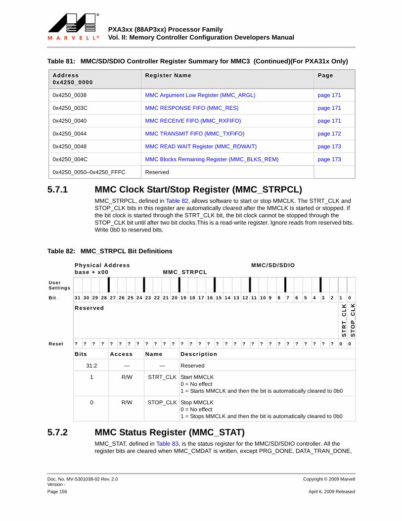
PXA3xx (88AP3xx) Processor Family Vol. II: Memory Controller Configuration Developers Manual
Doc. No. MV-S301038-02 Rev. 2.0 Version -
Copyright © 2009 Marvell
Page 156 April 6, 2009 Released
12345678910111213141516171819202122232425262728293031323334353637383940414243444546474849505152535455565758
5.7.1 MMC Clock Start/Stop Register (MMC_STRPCL)MMC_STRPCL, defined in Table 82, allows software to start or stop MMCLK. The STRT_CLK and STOP_CLK bits in this register are automatically cleared after the MMCLK is started or stopped. If the bit clock is started through the STRT_CLK bit, the bit clock cannot be stopped through the STOP_CLK bit until after two bit clocks.This is a read-write register. Ignore reads from reserved bits. Write 0b0 to reserved bits.
5.7.2 MMC Status Register (MMC_STAT)MMC_STAT, defined in Table 83, is the status register for the MMC/SD/SDIO controller. All the register bits are cleared when MMC_CMDAT is written, except PRG_DONE, DATA_TRAN_DONE,
0x4250_0038 MMC Argument Low Register (MMC_ARGL) page 171
0x4250_003C MMC RESPONSE FIFO (MMC_RES) page 171
0x4250_0040 MMC RECEIVE FIFO (MMC_RXFIFO) page 171
0x4250_0044 MMC TRANSMIT FIFO (MMC_TXFIFO) page 172
0x4250_0048 MMC READ WAIT Register (MMC_RDWAIT) page 173
0x4250_004C MMC Blocks Remaining Register (MMC_BLKS_REM) page 173
0x4250_0050–0x4250_FFFC Reserved
Table 81: MMC/SD/SDIO Controller Register Summary for MMC3 (Continued)(For PXA31x Only)
Address0x4250_0000
Register Name Page
Table 82: MMC_STRPCL Bit Definitions
Physical Addressbase + x00 MMC_STRPCL
MMC/SD/SDIO
User Settings
Bit 31 30 29 28 27 26 25 24 23 22 21 20 19 18 17 16 15 14 13 12 11 10 9 8 7 6 5 4 3 2 1 0
Reserved
ST
RT
_C
LK
ST
OP
_C
LK
Reset ? ? ? ? ? ? ? ? ? ? ? ? ? ? ? ? ? ? ? ? ? ? ? ? ? ? ? ? ? ? 0 0
Bits Access Name Descript ion
31:2 — — Reserved
1 R/W STRT_CLK Start MMCLK0 = No effect1 = Starts MMCLK and then the bit is automatically cleared to 0b0
0 R/W STOP_CLK Stop MMCLK0 = No effect1 = Stops MMCLK and then the bit is automatically cleared to 0b0

MultiMediaCard/SD/SDIO ControllerMMC/SD/SCIO Controller Registers
Copyright © 2009 Marvell Doc. No. MV-S301038-02 Rev. 2.0Version -
April 6, 2009 Released Page 157
12345678910111213141516171819202122232425262728293031323334353637383940414243444546474849505152535455565758
FLASH_ERR, CLK_EN, CRC_RD_ERR and CRC_WR_ERR, which are cleared if the new command does not perform a data transfer and the new command is not CMD52 for an SDIO suspend operation. CLK_EN is never reset—it always indicates the state of the MMCLK. Also, bit 6 is always set automatically.
In a system with multiple cards running in SPI mode, there is a limitation if the system has to interleave commands to both cards. For example, if programming Card 0, then switching to Card 1, then back to Card 0, the status register bits do not properly reflect the status of the card that is active. The workaround for this problem is to program the GPIO to monitor the SPI interface of interest and then poll the GPIO status register to obtain the status of either card.
This is a read-only register. Ignore reads from reserved bits.
Table 83: MMC_STAT Bit Definitions
Physical Addressbase + x04
MMC_STAT MMC/SD/SDIO
User Settings
Bit 31 30 29 28 27 26 25 24 23 22 21 20 19 18 17 16 15 14 13 12 11 10 9 8 7 6 5 4 3 2 1 0
ReservedS
DIO
_S
US
PE
ND
_A
CK
SD
IO_
INT
RD
_S
TA
LL
ED
EN
D_
CM
D_
RE
S
PR
G_
DO
NE
DA
TA
_T
RA
N_
DO
NE
SP
I_W
R_
ER
R
FL
AS
H_
ER
R
CL
K_
EN
Re
se
rve
d
Re
se
rve
d
RE
S_
CR
C_
ER
R
DA
T_
ER
R_
TO
KE
N
CR
C_
RD
_E
RR
CR
C_
WR
_E
RR
TIM
E_
OU
T_
RE
S
TIM
E_
OU
T_
RE
AD
Reset ? ? ? ? ? ? ? ? ? ? ? ? ? ? ? 0 0 0 0 0 0 0 0 0 0 1 0 0 0 0 0 0
Bits Access Name Descript ion
31:17 — — Reserved
16 R SDIO_SUSPEND_
ACK
SDIO Suspend Acknowledge0 = No suspend1 = SDIO data transfer suspended by SDIO card
15 R SDIO_INT SDIO Interrupt0 = No interrupt1 = SDIO interrupt
14 R RD_STALLED
Read Stalled0 = No stall1 = Read data transfer stalled in response to RD_WAIT
13 R END_CMD_RES
End Command Response0 = Command and response sequence not complete1 = Command and response sequence complete
12 R PRG_DONE Programming Done0 = Card has not finished programming and is busy1 = Card has finished programming and is not busy
11 R DATA_TRAN_DONE
Data Transmission Done0 = Data transmission to card not complete1 = Data transmission to card is complete

PXA3xx (88AP3xx) Processor Family Vol. II: Memory Controller Configuration Developers Manual
Doc. No. MV-S301038-02 Rev. 2.0 Version -
Copyright © 2009 Marvell
Page 158 April 6, 2009 Released
12345678910111213141516171819202122232425262728293031323334353637383940414243444546474849505152535455565758
10 R SPI_WR_ERR
SPI Write Error0 = No error 1 = Write data rejected by card due to a write error
9 R FLASH_ERR
FLASH Error0 = No error1 = Flash programming error
8 R CLK_EN MMCLK Enable0 = MMCLK is disabled1 = MMCLK is enabled
7:6 — — Reserved
5 R RES_CRC_ERR
Response CRC Error0 = No error1 = CRC error on the response
4 R DAT_ERR_TOKEN
Data Error Token0 = No error token1 = SPI data error token received
3 R CRC_RD_ERR
CRC Read Error0 = No error1 = CRC error on received data
2 R CRC_WR_ERR
CRC Write Error0 = No error1 = Write data rejected by card due to a CRC error
1 R TIME_OUT_RES
Time Out Response0 = No time out1 = Card response timed out
0 R TIME_OUT_READ
Time Out Read0 = No time out1 = Card read data timed out
Table 83: MMC_STAT Bit Definitions (Continued)
Physical Addressbase + x04
MMC_STAT MMC/SD/SDIO
User Settings
Bit 31 30 29 28 27 26 25 24 23 22 21 20 19 18 17 16 15 14 13 12 11 10 9 8 7 6 5 4 3 2 1 0
Reserved
SD
IO_
SU
SP
EN
D_
AC
K
SD
IO_
INT
RD
_S
TA
LL
ED
EN
D_
CM
D_
RE
S
PR
G_
DO
NE
DA
TA
_T
RA
N_
DO
NE
SP
I_W
R_
ER
R
FL
AS
H_
ER
R
CL
K_
EN
Re
se
rve
d
Re
se
rve
d
RE
S_
CR
C_
ER
R
DA
T_
ER
R_
TO
KE
N
CR
C_
RD
_E
RR
CR
C_
WR
_E
RR
TIM
E_
OU
T_
RE
S
TIM
E_
OU
T_
RE
AD
Reset ? ? ? ? ? ? ? ? ? ? ? ? ? ? ? 0 0 0 0 0 0 0 0 0 0 1 0 0 0 0 0 0
Bits Access Name Descript ion

MultiMediaCard/SD/SDIO ControllerMMC/SD/SCIO Controller Registers
Copyright © 2009 Marvell Doc. No. MV-S301038-02 Rev. 2.0Version -
April 6, 2009 Released Page 159
12345678910111213141516171819202122232425262728293031323334353637383940414243444546474849505152535455565758
5.7.3 MMC Clock Rate Register (MMC_CLKRT)MMC_CLKRT, defined in Table 84, specifies the frequency of MMCLK. Software should write to this register only after turning the clock off and an interrupt request is generated to indicate that MMCLK has been turned off, MMC_I_REG[CLK_IS_OFF]. This is a read-write register. Ignore reads from reserved bits. Write 0b0 to reserved bits.
5.7.4 MMC SPI Mode Register (MMC_SPI)MMC_SPI, defined in Table 85, configures the MMC/SD/SDIO controller for SPI mode. This register is for SPI mode only, and software configures it. Software must set both the SPI_MODE bit and the SPI_CS_EN bit to configure the MMC/SD/SDIO controller for SPI mode. Otherwise, the MMC/SD/SDIO controller remains in MMC/SD/SDIO mode. For example, if an SPI card is connected to the MMCCS1 pin, software must set each of the following bits:
SPI_MODESPI_CS_ENSPI_CS_ADDRESS must be set or cleared
In a system with multiple cards running in SPI mode, there is a limitation if the system has to interleave commands to both cards. For example, if programming Card 0, then switching to Card 1, then back to Card 0, the status register bits do not properly reflect the status of the card that is active. The workaround is to program the GPIO to monitor the SPI interface of interest, then poll the GPIO status register to obtain the status of either of the cards.
This is a read-write register. Ignore reads from reserved bits. Write 0b0 to reserved bits.
Table 84: MMC_CLKRT Bit Definitions
Physical Addressbase + x08
MMC_CLKRT MMC/SD/SDIO
User Settings
Bit 31 30 29 28 27 26 25 24 23 22 21 20 19 18 17 16 15 14 13 12 11 10 9 8 7 6 5 4 3 2 1 0
Reserved CLKRATE
Reset ? ? ? ? ? ? ? ? ? ? ? ? ? ? ? ? ? ? ? ? ? ? ? ? ? ? ? ? ? 0 0 0
Bits Access Name Description
31:3 — — Reserved
2:0 R/W CLK_RATE Clock Rate (MMCLK Frequency)000 = 19.5 MHz001 = 9.75 MHz (19.5 MHz / 2)010 = 4.88 MHz (19.5 MHz / 4)011 = 2.44 MHz (19.5 MHz / 8)100 = 1.22 MHz (19.5 MHz / 16)101 = 609 kHz (19.5 MHz / 32)110 = 304 kHz (19.5 MHz / 64)111 = 26 MHz

PXA3xx (88AP3xx) Processor Family Vol. II: Memory Controller Configuration Developers Manual
Doc. No. MV-S301038-02 Rev. 2.0 Version -
Copyright © 2009 Marvell
Page 160 April 6, 2009 Released
12345678910111213141516171819202122232425262728293031323334353637383940414243444546474849505152535455565758
5.7.5 MMC Command Data Register (MMC_CMDAT)MMC_CMDAT, shown in Table 86, controls the command sequence. When MMCLK is turned on, a software Write to this register starts the command sequence on the MMC/SD/SDIO bus. Writing MMC_CMDAT automatically clears the MMC_STAT register and automatically clears the MMC_RXFIFO and MMC_TXFIFO, except if the STOP_TRAN bit is written to an 0b1 or the command is SDIO CMD52.
For SDIO suspend/resume operations (CMD52), the data programmed into the MMC_CMDAT register must be set for the command that is to be suspended or resumed, not the actual CMD52 itself (bits 2 and 3 are commonly set incorrectly). The MMC/SDIO controller does not store the context of the command being suspended or resumed, so the appropriate bits must always be set even when current transactions are suspended or resumed.
If a command is to be sent in parallel with a data transfer, the SD_4DAT, DMA_EN, STRM_BLK, and WR_RD, DATA_EN data control bits must remain as set in the previous data transfer command. Also, read and write service from and to MMC_RXFIFO and MMC_TXFIFO, respectively, must continue during the overlapping command.
This is a read-write register. Ignore reads from reserved bits. Write 0b0 to reserved bits.
Table 85: MMC_SPI Bit Definitions
Physical Addressbase + x0c
MMC_SPI MMC/SD/SDIO
User Settings
Bit 31 30 29 28 27 26 25 24 23 22 21 20 19 18 17 16 15 14 13 12 11 10 9 8 7 6 5 4 3 2 1 0
Reserved
SP
I_C
S_
AD
DR
ES
S
SP
I_C
S_
EN
SP
I_C
RC
_E
N
SP
I_M
OD
E
Reset ? ? ? ? ? ? ? ? ? ? ? ? ? ? ? ? ? ? ? ? ? ? ? ? ? ? ? ? 0 0 0 0
Bits Access Name Descript ion
31:4 — — Reserved
3 R/W SPI_CS_ADDRESS
SPI Chip-Select Address0 = Enables the card connected to the MMCCS0 pin.1 = Enables the card connected to the MMCCS1 pin.
2 R/W SPI_CS_EN SPI Chip Select Enable0 = Disables the SPI chip select.1 = Enables the SPI chip select.
1 R/W SPI_CRC_EN
SPI CRC Generation Enable0 = Disables CRC generation and verification.1 = Enables CRC generation and verification.
0 R/W SPI_MODE SPI Mode0 = Disables SPI mode.1 = Enables SPI mode.
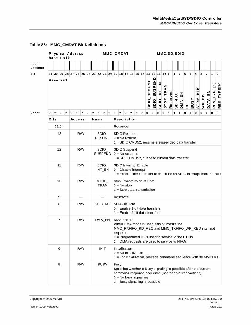
MultiMediaCard/SD/SDIO ControllerMMC/SD/SCIO Controller Registers
Copyright © 2009 Marvell Doc. No. MV-S301038-02 Rev. 2.0Version -
April 6, 2009 Released Page 161
12345678910111213141516171819202122232425262728293031323334353637383940414243444546474849505152535455565758
Table 86: MMC_CMDAT Bit Definitions
Physical Addressbase + x10
MMC_CMDAT MMC/SD/SDIO
User Settings
Bit 31 30 29 28 27 26 25 24 23 22 21 20 19 18 17 16 15 14 13 12 11 10 9 8 7 6 5 4 3 2 1 0
Reserved
SD
IO_
RE
SU
ME
SD
IO_
SU
SP
EN
D
SD
IO_
INT
_E
N
ST
OP
_T
RA
N
Re
se
rve
d
SD
_4
DA
T
DM
A_
EN
INIT
BU
SY
ST
RM
_B
LK
WR
_R
D
DA
TA
_E
N
RE
S_
TY
PE
[1]
RE
S_
TY
PE
[0]
Reset ? ? ? ? ? ? ? ? ? ? ? ? ? ? ? ? ? ? 0 0 0 0 ? 0 1 0 0 0 0 0 0 0
Bits Access Name Descript ion
31:14 — — Reserved
13 R/W SDIO_RESUME
SDIO Resume0 = No resume1 = SDIO CMD52, resume a suspended data transfer
12 R/W SDIO_SUSPEND
SDIO Suspend0 = No suspend1 = SDIO CMD52, suspend current data transfer
11 R/W SDIO_INT_EN
SDIO Interrupt Enable0 = Disable interrupt1 = Enables the controller to check for an SDIO interrupt from the card
10 R/W STOP_TRAN
Stop Transmission of Data0 = No stop1 = Stop data transmission
9 — — Reserved
8 R/W SD_4DAT SD 4-Bit Data0 = Enable 1-bit data transfers1 = Enable 4 bit data transfers
7 R/W DMA_EN DMA EnableWhen DMA mode is used, this bit masks the MMC_RXFIFO_RD_REQ and MMC_TXFIFO_WR_REQ interrupt requests.0 = Programmed IO is used to service to the FIFOs1 = DMA requests are used to service to FIFOs
6 R/W INIT Initialization0 = No initialization1 = For initialization, precede command sequence with 80 MMCLKs
5 R/W BUSY BusySpecifies whether a Busy signaling is possible after the current command-response sequence (not for data transactions)0 = No busy signalling1 = Busy signalling is possible

PXA3xx (88AP3xx) Processor Family Vol. II: Memory Controller Configuration Developers Manual
Doc. No. MV-S301038-02 Rev. 2.0 Version -
Copyright © 2009 Marvell
Page 162 April 6, 2009 Released
12345678910111213141516171819202122232425262728293031323334353637383940414243444546474849505152535455565758
4 R/W STRM_BLK Stream Block0 = Not in stream mode1 = Data transfer of current command sequence is in stream mode
3 R/W WR_RD Write Read0 = Current command sequence is for a read data transfer1 = Current command sequence is for a write data transfer
2 R/W DATA_EN Data Enable0 = No data transfer1 = Current command includes a data transfer
1:0 R/W RES_TYPE Response TypeResponse format for the current command (see Table 87)
Table 86: MMC_CMDAT Bit Definitions (Continued)
Physical Addressbase + x10
MMC_CMDAT MMC/SD/SDIO
User Settings
Bit 31 30 29 28 27 26 25 24 23 22 21 20 19 18 17 16 15 14 13 12 11 10 9 8 7 6 5 4 3 2 1 0
Reserved
SD
IO_
RE
SU
ME
SD
IO_
SU
SP
EN
D
SD
IO_
INT
_E
N
ST
OP
_T
RA
N
Re
se
rve
d
SD
_4
DA
T
DM
A_
EN
INIT
BU
SY
ST
RM
_B
LK
WR
_R
D
DA
TA
_E
N
RE
S_
TY
PE
[1]
RE
S_
TY
PE
[0]
Reset ? ? ? ? ? ? ? ? ? ? ? ? ? ? ? ? ? ? 0 0 0 0 ? 0 1 0 0 0 0 0 0 0
Bits Access Name Descript ion
Table 87: CMD_DAT_CONT RES_TYPE Bit Field Encoding
Response Format
RES_TYPE
MMC SD SDIO MMC - SPI SD–SPI SDIO– SPI
0b00 No Response
0b01 R1,R4,R56 bytes
R1,R66 bytes
R1,R4,R5,R66 bytes
R11 byte
R11 byte
R11 byte
0b10 R217 bytes
R217 bytes
R217 bytes
R22 bytes
R22 bytes
R2,R52 bytes
0b11 R36 bytes
R36 bytes
R36 bytes
R35 bytes
R35 bytes
R3,R45 bytes
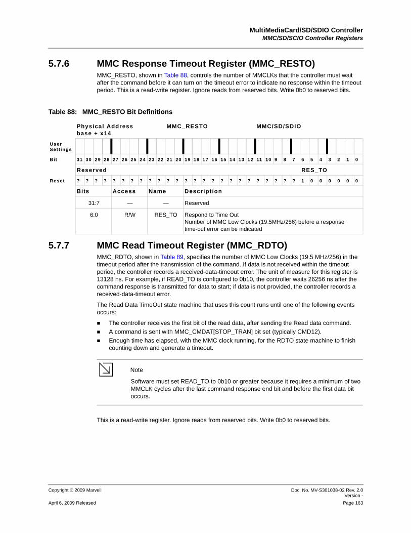
MultiMediaCard/SD/SDIO ControllerMMC/SD/SCIO Controller Registers
Copyright © 2009 Marvell Doc. No. MV-S301038-02 Rev. 2.0Version -
April 6, 2009 Released Page 163
12345678910111213141516171819202122232425262728293031323334353637383940414243444546474849505152535455565758
5.7.6 MMC Response Timeout Register (MMC_RESTO)MMC_RESTO, shown in Table 88, controls the number of MMCLKs that the controller must wait after the command before it can turn on the timeout error to indicate no response within the timeout period. This is a read-write register. Ignore reads from reserved bits. Write 0b0 to reserved bits.
5.7.7 MMC Read Timeout Register (MMC_RDTO)MMC_RDTO, shown in Table 89, specifies the number of MMC Low Clocks (19.5 MHz/256) in the timeout period after the transmission of the command. If data is not received within the timeout period, the controller records a received-data-timeout error. The unit of measure for this register is 13128 ns. For example, if READ_TO is configured to 0b10, the controller waits 26256 ns after the command response is transmitted for data to start; if data is not provided, the controller records a received-data-timeout error.
The Read Data TimeOut state machine that uses this count runs until one of the following events occurs:
The controller receives the first bit of the read data, after sending the Read data command.A command is sent with MMC_CMDAT[STOP_TRAN] bit set (typically CMD12).
Enough time has elapsed, with the MMC clock running, for the RDTO state machine to finish counting down and generate a timeout.
Note
Note Software must set READ_TO to 0b10 or greater because it requires a minimum of two MMCLK cycles after the last command response end bit and before the first data bit occurs.
This is a read-write register. Ignore reads from reserved bits. Write 0b0 to reserved bits.
Table 88: MMC_RESTO Bit Definitions
Physical Addressbase + x14
MMC_RESTO MMC/SD/SDIO
User Settings
Bit 31 30 29 28 27 26 25 24 23 22 21 20 19 18 17 16 15 14 13 12 11 10 9 8 7 6 5 4 3 2 1 0
Reserved RES_TO
Reset ? ? ? ? ? ? ? ? ? ? ? ? ? ? ? ? ? ? ? ? ? ? ? ? ? 1 0 0 0 0 0 0
Bits Access Name Descript ion
31:7 — — Reserved
6:0 R/W RES_TO Respond to Time OutNumber of MMC Low Clocks (19.5MHz/256) before a response time-out error can be indicated
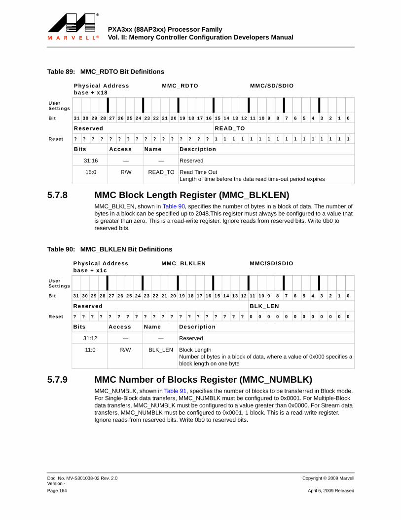
PXA3xx (88AP3xx) Processor Family Vol. II: Memory Controller Configuration Developers Manual
Doc. No. MV-S301038-02 Rev. 2.0 Version -
Copyright © 2009 Marvell
Page 164 April 6, 2009 Released
12345678910111213141516171819202122232425262728293031323334353637383940414243444546474849505152535455565758
5.7.8 MMC Block Length Register (MMC_BLKLEN)MMC_BLKLEN, shown in Table 90, specifies the number of bytes in a block of data. The number of bytes in a block can be specified up to 2048.This register must always be configured to a value that is greater than zero. This is a read-write register. Ignore reads from reserved bits. Write 0b0 to reserved bits.
5.7.9 MMC Number of Blocks Register (MMC_NUMBLK)MMC_NUMBLK, shown in Table 91, specifies the number of blocks to be transferred in Block mode. For Single-Block data transfers, MMC_NUMBLK must be configured to 0x0001. For Multiple-Block data transfers, MMC_NUMBLK must be configured to a value greater than 0x0000. For Stream data transfers, MMC_NUMBLK must be configured to 0x0001, 1 block. This is a read-write register. Ignore reads from reserved bits. Write 0b0 to reserved bits.
Table 89: MMC_RDTO Bit Definitions
Physical Addressbase + x18
MMC_RDTO MMC/SD/SDIO
User Settings
Bit 31 30 29 28 27 26 25 24 23 22 21 20 19 18 17 16 15 14 13 12 11 10 9 8 7 6 5 4 3 2 1 0
Reserved READ_TO
Reset ? ? ? ? ? ? ? ? ? ? ? ? ? ? ? ? 1 1 1 1 1 1 1 1 1 1 1 1 1 1 1 1
Bits Access Name Descript ion
31:16 — — Reserved
15:0 R/W READ_TO Read Time OutLength of time before the data read time-out period expires
Table 90: MMC_BLKLEN Bit Definitions
Physical Addressbase + x1c
MMC_BLKLEN MMC/SD/SDIO
User Settings
Bit 31 30 29 28 27 26 25 24 23 22 21 20 19 18 17 16 15 14 13 12 11 10 9 8 7 6 5 4 3 2 1 0
Reserved BLK_LEN
Reset ? ? ? ? ? ? ? ? ? ? ? ? ? ? ? ? ? ? ? ? 0 0 0 0 0 0 0 0 0 0 0 0
Bits Access Name Descript ion
31:12 — — Reserved
11:0 R/W BLK_LEN Block LengthNumber of bytes in a block of data, where a value of 0x000 specifies a block length on one byte
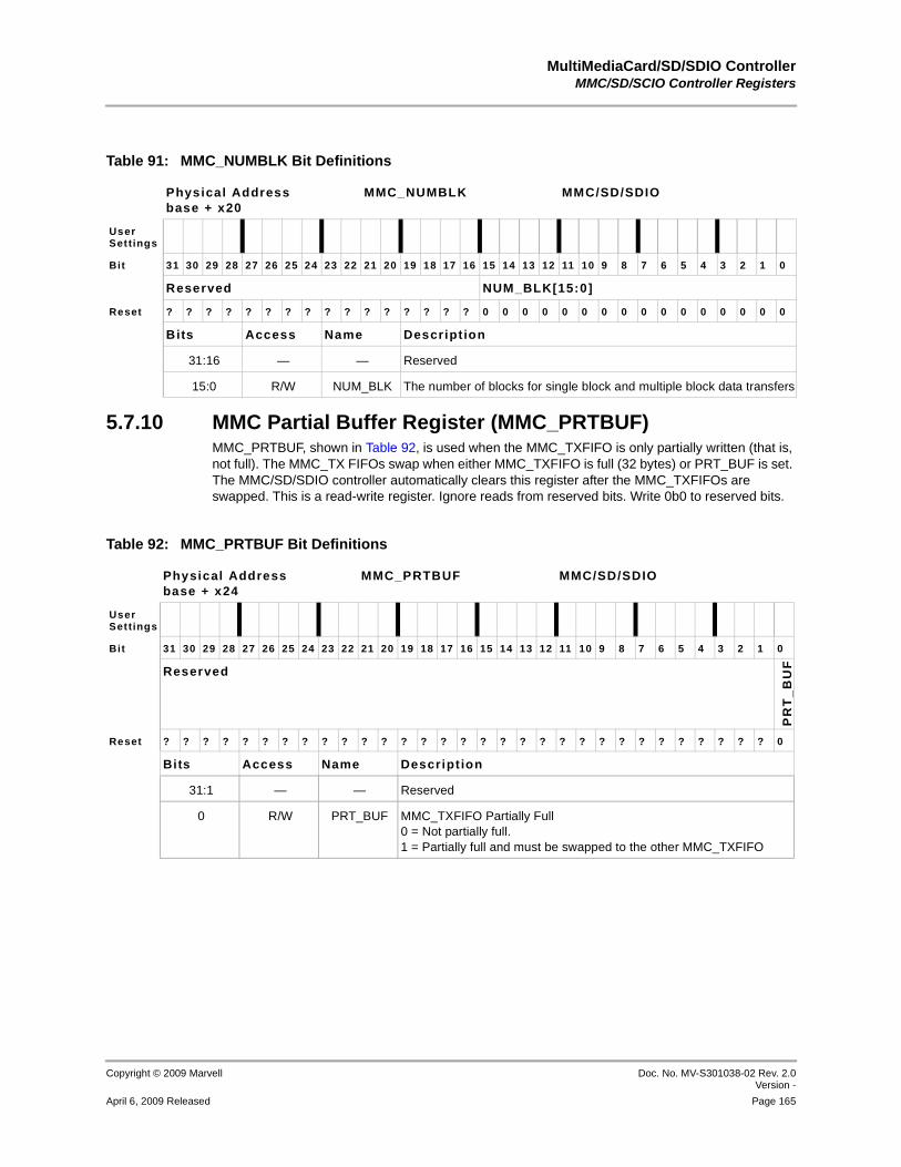
MultiMediaCard/SD/SDIO ControllerMMC/SD/SCIO Controller Registers
Copyright © 2009 Marvell Doc. No. MV-S301038-02 Rev. 2.0Version -
April 6, 2009 Released Page 165
12345678910111213141516171819202122232425262728293031323334353637383940414243444546474849505152535455565758
5.7.10 MMC Partial Buffer Register (MMC_PRTBUF)MMC_PRTBUF, shown in Table 92, is used when the MMC_TXFIFO is only partially written (that is, not full). The MMC_TX FIFOs swap when either MMC_TXFIFO is full (32 bytes) or PRT_BUF is set. The MMC/SD/SDIO controller automatically clears this register after the MMC_TXFIFOs are swapped. This is a read-write register. Ignore reads from reserved bits. Write 0b0 to reserved bits.
Table 91: MMC_NUMBLK Bit Definitions
Physical Addressbase + x20
MMC_NUMBLK MMC/SD/SDIO
User Settings
Bit 31 30 29 28 27 26 25 24 23 22 21 20 19 18 17 16 15 14 13 12 11 10 9 8 7 6 5 4 3 2 1 0
Reserved NUM_BLK[15:0]
Reset ? ? ? ? ? ? ? ? ? ? ? ? ? ? ? ? 0 0 0 0 0 0 0 0 0 0 0 0 0 0 0 0
Bits Access Name Descript ion
31:16 — — Reserved
15:0 R/W NUM_BLK The number of blocks for single block and multiple block data transfers
Table 92: MMC_PRTBUF Bit Definitions
Physical Addressbase + x24
MMC_PRTBUF MMC/SD/SDIO
User Settings
Bit 31 30 29 28 27 26 25 24 23 22 21 20 19 18 17 16 15 14 13 12 11 10 9 8 7 6 5 4 3 2 1 0
Reserved
PR
T_
BU
F
Reset ? ? ? ? ? ? ? ? ? ? ? ? ? ? ? ? ? ? ? ? ? ? ? ? ? ? ? ? ? ? ? 0
Bits Access Name Descript ion
31:1 — — Reserved
0 R/W PRT_BUF MMC_TXFIFO Partially Full0 = Not partially full.1 = Partially full and must be swapped to the other MMC_TXFIFO

PXA3xx (88AP3xx) Processor Family Vol. II: Memory Controller Configuration Developers Manual
Doc. No. MV-S301038-02 Rev. 2.0 Version -
Copyright © 2009 Marvell
Page 166 April 6, 2009 Released
12345678910111213141516171819202122232425262728293031323334353637383940414243444546474849505152535455565758
5.7.11 MMC Interrupt Mask Register (MMC_I_MASK)MMC_I_MASK, shown in Table 93, enables or disables the various interrupt conditions. To disable a specific interrupt condition, set its corresponding mask bit. This is a read-write register. Ignore reads from reserved bits. Write 0b0 to reserved bits.
Table 93: MMC_I_MASK Bit Definitions
Physical Addressbase + x28
MMC_I_MASK MMC/SD/SDIO
User Settings
Bit 31 30 29 28 27 26 25 24 23 22 21 20 19 18 17 16 15 14 13 12 11 10 9 8 7 6 5 4 3 2 1 0
Reserved
SD
IO_
SU
SP
EN
D_
AC
K
SD
IO_
INT
RD
_S
TA
LL
ED
RE
S_
ER
R
DA
T_
ER
R
TIN
T
MM
C_
TX
FIF
O_
WR
_R
EQ
MM
C_
RX
FIF
O_
RD
_R
EQ
CL
K_
IS_
OF
F
ST
OP
_C
MD
EN
D_
CM
D_
RE
S
PR
G_
DO
NE
DA
TA
_T
RA
N_
DO
NE
Reset ? ? ? ? ? ? ? ? ? ? ? ? ? ? ? ? ? ? ? 1 1 1 1 1 1 1 1 1 1 1 1 1
Bits Access Name Descript ion
31:13 — — Reserved
12 R/W SDIO_SUSPEND_
ACK
SDIO Suspend Acknowledge0 = Enabled1 = Masked
11 R/W SDIO_INT SDIO Interrupt0 = Enabled1 = Masked
10 R/W RD_STALLED Read Stalled0 = Enabled1 = Masked
9 R/W RES_ERR Response Error0 = Enabled1 = Masked
8 R/W DAT_ERR Data Error0 = Enabled1 = Masked
7 R/W TINT Timeout Interrupt0 = Enabled1 = Masked
6 R/W TXFIFO_WR_REQ
TXFIFO Write Request0 = Enabled1 = Masked
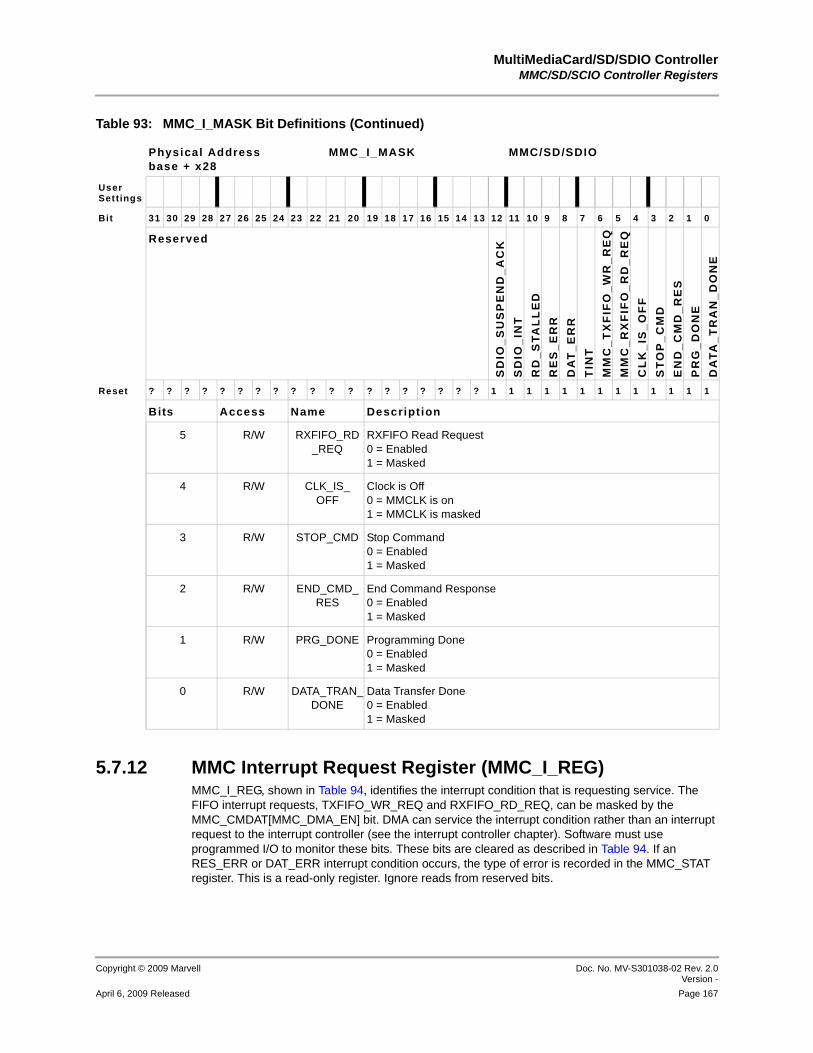
MultiMediaCard/SD/SDIO ControllerMMC/SD/SCIO Controller Registers
Copyright © 2009 Marvell Doc. No. MV-S301038-02 Rev. 2.0Version -
April 6, 2009 Released Page 167
12345678910111213141516171819202122232425262728293031323334353637383940414243444546474849505152535455565758
5.7.12 MMC Interrupt Request Register (MMC_I_REG)MMC_I_REG, shown in Table 94, identifies the interrupt condition that is requesting service. The FIFO interrupt requests, TXFIFO_WR_REQ and RXFIFO_RD_REQ, can be masked by the MMC_CMDAT[MMC_DMA_EN] bit. DMA can service the interrupt condition rather than an interrupt request to the interrupt controller (see the interrupt controller chapter). Software must use programmed I/O to monitor these bits. These bits are cleared as described in Table 94. If an RES_ERR or DAT_ERR interrupt condition occurs, the type of error is recorded in the MMC_STAT register. This is a read-only register. Ignore reads from reserved bits.
5 R/W RXFIFO_RD_REQ
RXFIFO Read Request0 = Enabled1 = Masked
4 R/W CLK_IS_OFF
Clock is Off0 = MMCLK is on1 = MMCLK is masked
3 R/W STOP_CMD Stop Command0 = Enabled1 = Masked
2 R/W END_CMD_RES
End Command Response0 = Enabled1 = Masked
1 R/W PRG_DONE Programming Done0 = Enabled1 = Masked
0 R/W DATA_TRAN_DONE
Data Transfer Done0 = Enabled1 = Masked
Table 93: MMC_I_MASK Bit Definitions (Continued)
Physical Addressbase + x28
MMC_I_MASK MMC/SD/SDIO
User Settings
Bit 31 30 29 28 27 26 25 24 23 22 21 20 19 18 17 16 15 14 13 12 11 10 9 8 7 6 5 4 3 2 1 0
Reserved
SD
IO_
SU
SP
EN
D_
AC
K
SD
IO_
INT
RD
_S
TA
LL
ED
RE
S_
ER
R
DA
T_
ER
R
TIN
T
MM
C_
TX
FIF
O_
WR
_R
EQ
MM
C_
RX
FIF
O_
RD
_R
EQ
CL
K_
IS_
OF
F
ST
OP
_C
MD
EN
D_
CM
D_
RE
S
PR
G_
DO
NE
DA
TA
_T
RA
N_
DO
NE
Reset ? ? ? ? ? ? ? ? ? ? ? ? ? ? ? ? ? ? ? 1 1 1 1 1 1 1 1 1 1 1 1 1
Bits Access Name Descript ion
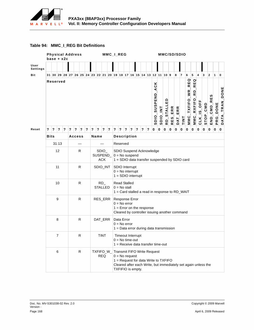
PXA3xx (88AP3xx) Processor Family Vol. II: Memory Controller Configuration Developers Manual
Doc. No. MV-S301038-02 Rev. 2.0 Version -
Copyright © 2009 Marvell
Page 168 April 6, 2009 Released
12345678910111213141516171819202122232425262728293031323334353637383940414243444546474849505152535455565758
Table 94: MMC_I_REG Bit Definitions
Physical Addressbase + x2c
MMC_I_REG MMC/SD/SDIO
User Settings
Bit 31 30 29 28 27 26 25 24 23 22 21 20 19 18 17 16 15 14 13 12 11 10 9 8 7 6 5 4 3 2 1 0
Reserved
SD
IO_
SU
SP
EN
D_
AC
K
SD
IO_
INT
RD
_S
TA
LL
ED
RE
S_
ER
R
DA
T_
ER
R
TIN
T
MM
C_
TX
FIF
O_
WR
_R
EQ
MM
C_
RX
FIF
O_
RD
_R
EQ
CL
K_
IS_
OF
F
ST
OP
_C
MD
EN
D_
CM
D_
RE
S
PR
G_
DO
NE
DA
TA
_T
RA
N_
DO
NE
Reset ? ? ? ? ? ? ? ? ? ? ? ? ? ? ? ? ? ? ? 0 0 0 0 0 0 0 0 0 0 0 0 0
Bits Access Name Descript ion
31:13 — — Reserved
12 R SDIO_SUSPEND_
ACK
SDIO Suspend Acknowledge0 = No suspend1 = SDIO data transfer suspended by SDIO card
11 R SDIO_INT SDIO Interrupt0 = No interrupt 1 = SDIO interrupt
10 R RD_STALLED
Read Stalled0 = No stall1 = Card stalled a read in response to RD_WAIT
9 R RES_ERR Response Error0 = No error1 = Error on the responseCleared by controller issuing another command
8 R DAT_ERR Data Error0 = No error1 = Data error during data transmission
7 R TINT Timeout Interrupt0 = No time-out1 = Receive data transfer time-out
6 R TXFIFO_W_REQ
Transmit FIFO Write Request0 = No request1 = Request for data Write to TXFIFO Cleared after each Write, but immediately set again unless the TXFIFIO is empty.
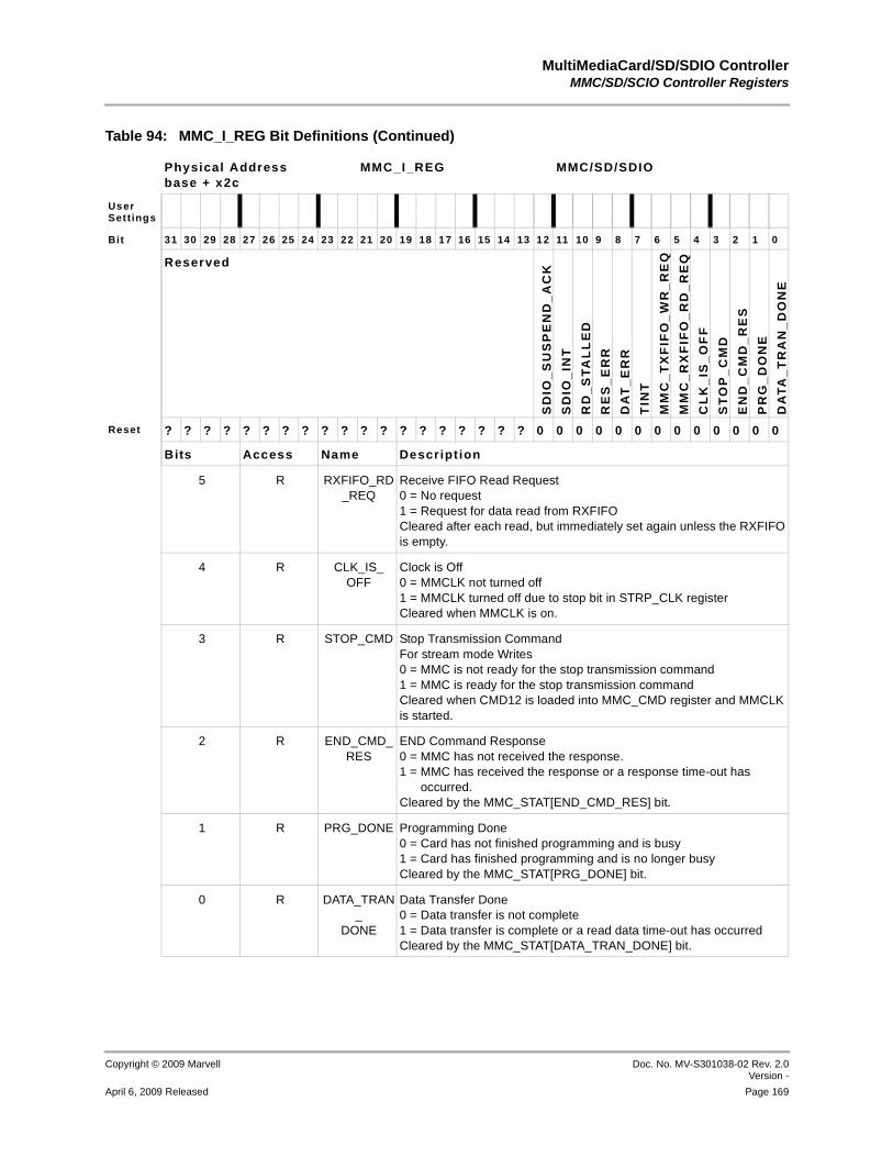
MultiMediaCard/SD/SDIO ControllerMMC/SD/SCIO Controller Registers
Copyright © 2009 Marvell Doc. No. MV-S301038-02 Rev. 2.0Version -
April 6, 2009 Released Page 169
12345678910111213141516171819202122232425262728293031323334353637383940414243444546474849505152535455565758
5 R RXFIFO_RD_REQ
Receive FIFO Read Request0 = No request1 = Request for data read from RXFIFOCleared after each read, but immediately set again unless the RXFIFO is empty.
4 R CLK_IS_OFF
Clock is Off0 = MMCLK not turned off1 = MMCLK turned off due to stop bit in STRP_CLK registerCleared when MMCLK is on.
3 R STOP_CMD Stop Transmission CommandFor stream mode Writes0 = MMC is not ready for the stop transmission command1 = MMC is ready for the stop transmission commandCleared when CMD12 is loaded into MMC_CMD register and MMCLK is started.
2 R END_CMD_RES
END Command Response0 = MMC has not received the response.1 = MMC has received the response or a response time-out has
occurred.Cleared by the MMC_STAT[END_CMD_RES] bit.
1 R PRG_DONE Programming Done0 = Card has not finished programming and is busy1 = Card has finished programming and is no longer busyCleared by the MMC_STAT[PRG_DONE] bit.
0 R DATA_TRAN_
DONE
Data Transfer Done0 = Data transfer is not complete1 = Data transfer is complete or a read data time-out has occurredCleared by the MMC_STAT[DATA_TRAN_DONE] bit.
Table 94: MMC_I_REG Bit Definitions (Continued)
Physical Addressbase + x2c
MMC_I_REG MMC/SD/SDIO
User Settings
Bit 31 30 29 28 27 26 25 24 23 22 21 20 19 18 17 16 15 14 13 12 11 10 9 8 7 6 5 4 3 2 1 0
Reserved
SD
IO_
SU
SP
EN
D_
AC
K
SD
IO_
INT
RD
_S
TA
LL
ED
RE
S_
ER
R
DA
T_
ER
R
TIN
T
MM
C_
TX
FIF
O_
WR
_R
EQ
MM
C_
RX
FIF
O_
RD
_R
EQ
CL
K_
IS_
OF
F
ST
OP
_C
MD
EN
D_
CM
D_
RE
S
PR
G_
DO
NE
DA
TA
_T
RA
N_
DO
NE
Reset ? ? ? ? ? ? ? ? ? ? ? ? ? ? ? ? ? ? ? 0 0 0 0 0 0 0 0 0 0 0 0 0
Bits Access Name Descript ion

PXA3xx (88AP3xx) Processor Family Vol. II: Memory Controller Configuration Developers Manual
Doc. No. MV-S301038-02 Rev. 2.0 Version -
Copyright © 2009 Marvell
Page 170 April 6, 2009 Released
12345678910111213141516171819202122232425262728293031323334353637383940414243444546474849505152535455565758
5.7.13 MMC Command Register (MMC_CMD)MMC_CMD, shown in Table 95, specifies the command index. This is a read-write register. Ignore reads from reserved bits. Write 0b0 to reserved bits.
5.7.14 MMC Argument High Register (MMC_ARGH)MMC_ARGH, shown in Table 96, specifies the upper 16 bits of the argument for the current command. This is a read-write register. Ignore reads from reserved bits. Write 0b0 to reserved bits.
Table 95: MMC_CMD Bit Definitions
Physical Addressbase + x30
MMC_CMD MMC/SD/SDIO
User Settings
Bit 31 30 29 28 27 26 25 24 23 22 21 20 19 18 17 16 15 14 13 12 11 10 9 8 7 6 5 4 3 2 1 0
Reserved CMD_INDX
Reset ? ? ? ? ? ? ? ? ? ? ? ? ? ? ? ? ? ? ? ? ? ? ? ? 0 1 0 0 0 0 0 0
Bits Access Name Descript ion
31:6 — — Reserved
5:0 R/W CMD_INDX Command Index
Table 96: MMC_ARGH Bit Definitions
Physical Addressbase + x34
MMC_ARGH MMC/SD/SDIO
User Settings
Bit 31 30 29 28 27 26 25 24 23 22 21 20 19 18 17 16 15 14 13 12 11 10 9 8 7 6 5 4 3 2 1 0
Reserved ARG_H
Reset ? ? ? ? ? ? ? ? ? ? ? ? ? ? ? ? 0 0 0 0 0 0 0 0 0 0 0 0 0 0 0 0
Bits Access Name Descript ion
31:16 — — Reserved
15:0 R/W ARG_H Upper 16 bits of command argument
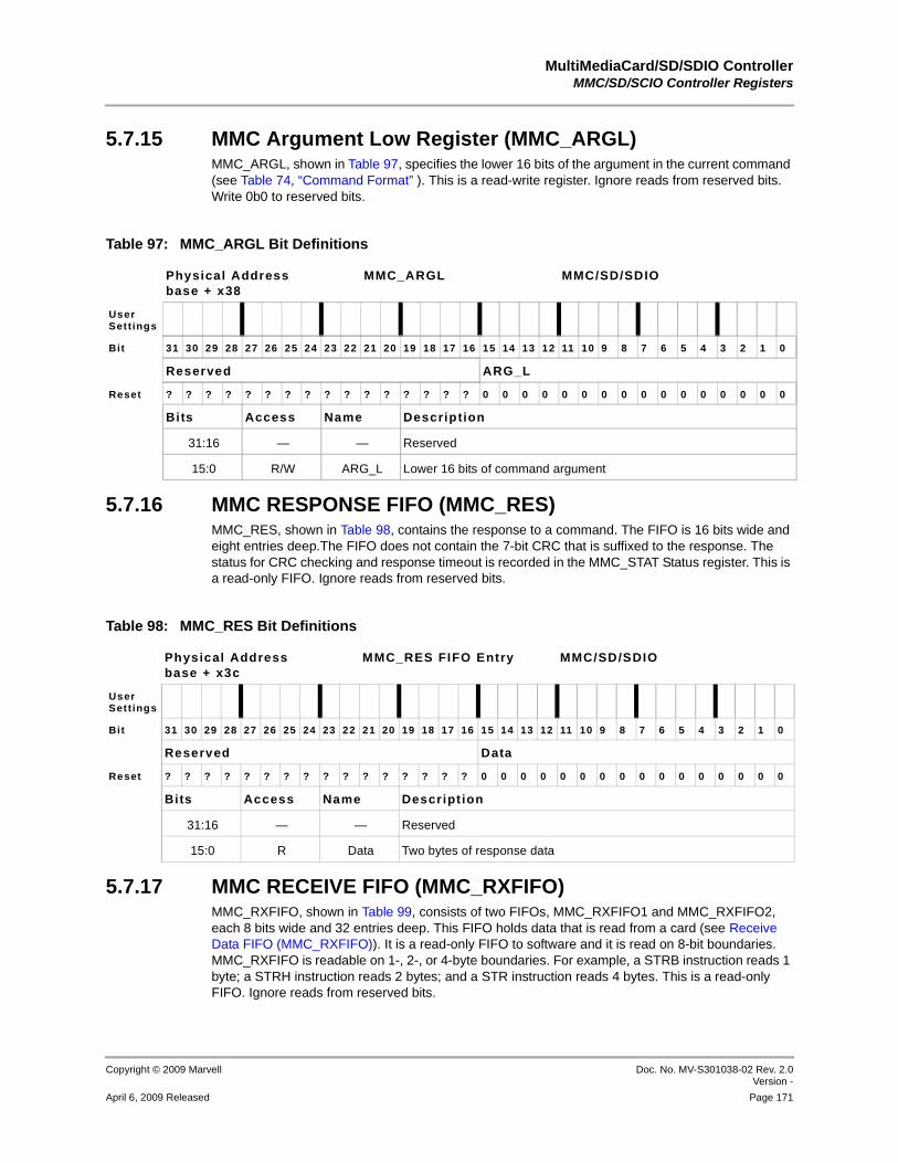
MultiMediaCard/SD/SDIO ControllerMMC/SD/SCIO Controller Registers
Copyright © 2009 Marvell Doc. No. MV-S301038-02 Rev. 2.0Version -
April 6, 2009 Released Page 171
12345678910111213141516171819202122232425262728293031323334353637383940414243444546474849505152535455565758
5.7.15 MMC Argument Low Register (MMC_ARGL)MMC_ARGL, shown in Table 97, specifies the lower 16 bits of the argument in the current command (see Table 74, “Command Format” ). This is a read-write register. Ignore reads from reserved bits. Write 0b0 to reserved bits.
5.7.16 MMC RESPONSE FIFO (MMC_RES)MMC_RES, shown in Table 98, contains the response to a command. The FIFO is 16 bits wide and eight entries deep.The FIFO does not contain the 7-bit CRC that is suffixed to the response. The status for CRC checking and response timeout is recorded in the MMC_STAT Status register. This is a read-only FIFO. Ignore reads from reserved bits.
5.7.17 MMC RECEIVE FIFO (MMC_RXFIFO)MMC_RXFIFO, shown in Table 99, consists of two FIFOs, MMC_RXFIFO1 and MMC_RXFIFO2, each 8 bits wide and 32 entries deep. This FIFO holds data that is read from a card (see Receive Data FIFO (MMC_RXFIFO)). It is a read-only FIFO to software and it is read on 8-bit boundaries. MMC_RXFIFO is readable on 1-, 2-, or 4-byte boundaries. For example, a STRB instruction reads 1 byte; a STRH instruction reads 2 bytes; and a STR instruction reads 4 bytes. This is a read-only FIFO. Ignore reads from reserved bits.
Table 97: MMC_ARGL Bit Definitions
Physical Addressbase + x38
MMC_ARGL MMC/SD/SDIO
User Settings
Bit 31 30 29 28 27 26 25 24 23 22 21 20 19 18 17 16 15 14 13 12 11 10 9 8 7 6 5 4 3 2 1 0
Reserved ARG_L
Reset ? ? ? ? ? ? ? ? ? ? ? ? ? ? ? ? 0 0 0 0 0 0 0 0 0 0 0 0 0 0 0 0
Bits Access Name Description
31:16 — — Reserved
15:0 R/W ARG_L Lower 16 bits of command argument
Table 98: MMC_RES Bit Definitions
Physical Addressbase + x3c
MMC_RES FIFO Entry MMC/SD/SDIO
User Settings
Bit 31 30 29 28 27 26 25 24 23 22 21 20 19 18 17 16 15 14 13 12 11 10 9 8 7 6 5 4 3 2 1 0
Reserved Data
Reset ? ? ? ? ? ? ? ? ? ? ? ? ? ? ? ? 0 0 0 0 0 0 0 0 0 0 0 0 0 0 0 0
Bits Access Name Descript ion
31:16 — — Reserved
15:0 R Data Two bytes of response data

PXA3xx (88AP3xx) Processor Family Vol. II: Memory Controller Configuration Developers Manual
Doc. No. MV-S301038-02 Rev. 2.0 Version -
Copyright © 2009 Marvell
Page 172 April 6, 2009 Released
12345678910111213141516171819202122232425262728293031323334353637383940414243444546474849505152535455565758
5.7.18 MMC TRANSMIT FIFO (MMC_TXFIFO)MMC_TXFIFO, shown in Table 100, consists of two FIFOs, MMC_TXFIFO1 and MMC_TXFIFO2, each 8 bits wide and 32 entries deep. This FIFO holds the data that is to be written to a card. It is a write-only FIFO to the software and it is written on boundaries 8 bits wide. MMC_TXFIFO is writable on 1-, 2-, or 4-byte boundaries. For example, a LDRB instruction, writes 1 byte; a LDRH instruction, writes 2 bytes; and a LDR instruction, writes 4 bytes. This is a write-only FIFO. Write 0b0 to reserved bits.
Table 99: MMC_RXFIFO Bit Definitions
Physical Addressbase + x040
MMC_RXFIFO, FIFO Entry MMC/SD/SDIO
User Settings
Bit 31 30 29 28 27 26 25 24 23 22 21 20 19 18 17 16 15 14 13 12 11 10 9 8 7 6 5 4 3 2 1 0
Reserved Data
Reset ? ? ? ? ? ? ? ? ? ? ? ? ? ? ? ? ? ? ? ? ? ? ? ? 0 0 0 0 0 0 0 0
Bits Access Name Descript ion
31:8 — — Reserved
7:0 R Data One, two, or four bytes of data received from a card
Table 100: MMC_TXFIFO Bit Definitions
Physical Addressbase + x044
MMC_TXFIFO, FIFO Entry MMC/SD/SDIO
User Settings
Bit 31 30 29 28 27 26 25 24 23 22 21 20 19 18 17 16 15 14 13 12 11 10 9 8 7 6 5 4 3 2 1 0
Reserved Data
Reset ? ? ? ? ? ? ? ? ? ? ? ? ? ? ? ? ? ? ? ? ? ? ? ? 0 0 0 0 0 0 0 0
Bits Access Name Descript ion
31:8 — — Reserved
7:0 W Data One, two, or four bytes of data to be transmitted to a card
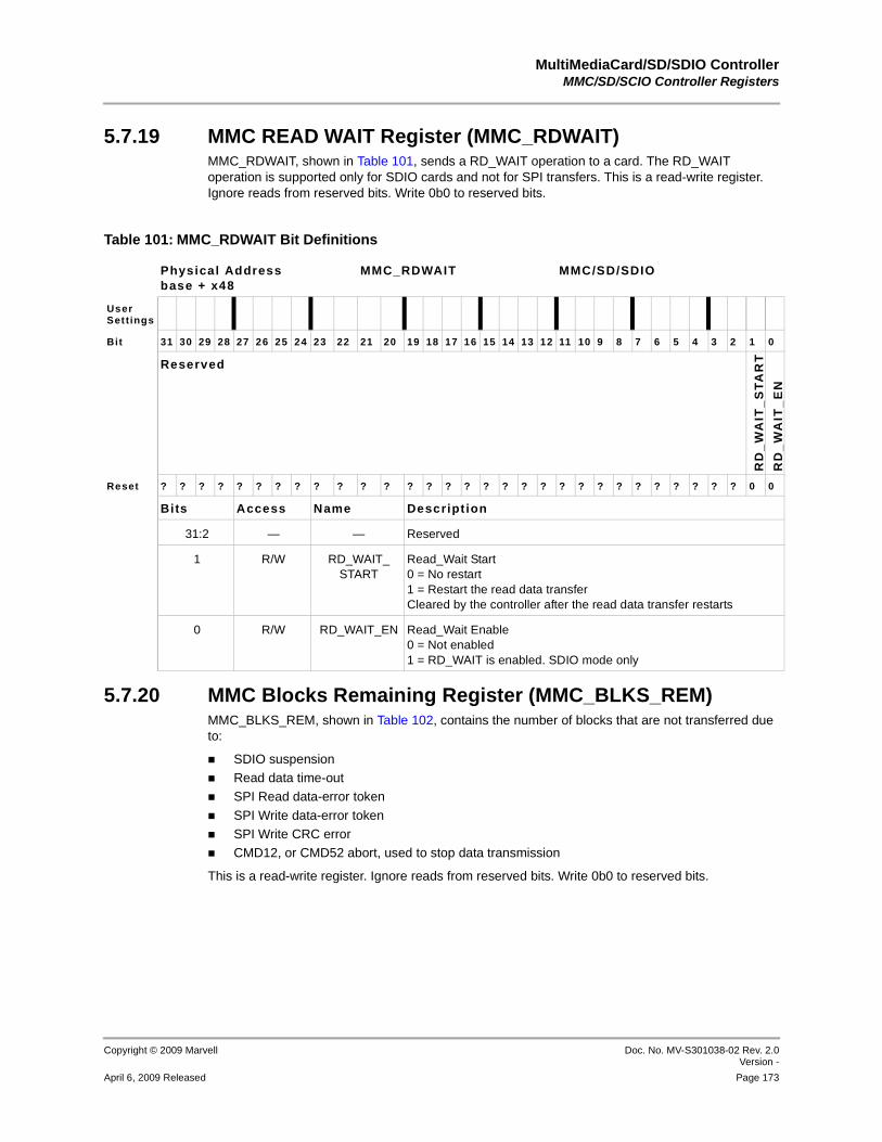
MultiMediaCard/SD/SDIO ControllerMMC/SD/SCIO Controller Registers
Copyright © 2009 Marvell Doc. No. MV-S301038-02 Rev. 2.0Version -
April 6, 2009 Released Page 173
12345678910111213141516171819202122232425262728293031323334353637383940414243444546474849505152535455565758
5.7.19 MMC READ WAIT Register (MMC_RDWAIT)MMC_RDWAIT, shown in Table 101, sends a RD_WAIT operation to a card. The RD_WAIT operation is supported only for SDIO cards and not for SPI transfers. This is a read-write register. Ignore reads from reserved bits. Write 0b0 to reserved bits.
5.7.20 MMC Blocks Remaining Register (MMC_BLKS_REM)MMC_BLKS_REM, shown in Table 102, contains the number of blocks that are not transferred due to:
SDIO suspensionRead data time-outSPI Read data-error token
SPI Write data-error tokenSPI Write CRC errorCMD12, or CMD52 abort, used to stop data transmission
This is a read-write register. Ignore reads from reserved bits. Write 0b0 to reserved bits.
Table 101: MMC_RDWAIT Bit Definitions
Physical Addressbase + x48
MMC_RDWAIT MMC/SD/SDIO
User Settings
Bit 31 30 29 28 27 26 25 24 23 22 21 20 19 18 17 16 15 14 13 12 11 10 9 8 7 6 5 4 3 2 1 0
Reserved
RD
_W
AIT
_S
TA
RT
RD
_W
AIT
_E
N
Reset ? ? ? ? ? ? ? ? ? ? ? ? ? ? ? ? ? ? ? ? ? ? ? ? ? ? ? ? ? ? 0 0
Bits Access Name Descript ion
31:2 — — Reserved
1 R/W RD_WAIT_START
Read_Wait Start0 = No restart1 = Restart the read data transferCleared by the controller after the read data transfer restarts
0 R/W RD_WAIT_EN Read_Wait Enable0 = Not enabled1 = RD_WAIT is enabled. SDIO mode only
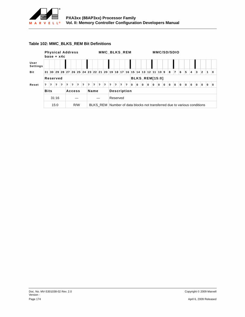
PXA3xx (88AP3xx) Processor Family Vol. II: Memory Controller Configuration Developers Manual
Doc. No. MV-S301038-02 Rev. 2.0 Version -
Copyright © 2009 Marvell
Page 174 April 6, 2009 Released
12345678910111213141516171819202122232425262728293031323334353637383940414243444546474849505152535455565758
Table 102: MMC_BLKS_REM Bit Definitions
Physical Addressbase + x4c
MMC_BLKS_REM MMC/SD/SDIO
User Settings
Bit 31 30 29 28 27 26 25 24 23 22 21 20 19 18 17 16 15 14 13 12 11 10 9 8 7 6 5 4 3 2 1 0
Reserved BLKS_REM[15:0]
Reset ? ? ? ? ? ? ? ? ? ? ? ? ? ? ? ? 0 0 0 0 0 0 0 0 0 0 0 0 0 0 0 0
Bits Access Name Descript ion
31:16 — — Reserved
15:0 R/W BLKS_REM Number of data blocks not transferred due to various conditions

MultiMediaCard/SD/SDIO ControllerMMC/SD/SCIO Controller Registers
Copyright © 2009 Marvell Doc. No. MV-S301038-02 Rev. 2.0Version -
April 6, 2009 Released Page 175
12345678910111213141516171819202122232425262728293031323334353637383940414243444546474849505152535455565758

Marvell. Moving Forward Faster
Marvell Semiconductor, Inc.5488 Marvell Lane
Santa Clara, CA 95054, USA
Tel: 1.408.222.2500Fax: 1.408.752.9028
www.marvell.com
Back Cover