marvell - storage - 88rc9580 datasheet · 2020-02-07 · marvell. marvell retains the right to make...
TRANSCRIPT

Doc No. MV-S104982-00 Rev. H
January 20, 2014
Document Classification: ProprietaryMarvell. Moving Forward Faster
88RC9580 R2.3Eight-Lane PCIe 2.0 to Eight-Port SAS/SATA 6 Gbps RAID-on-Chip Processor
Preliminary Datasheet

88RC9580 R2.3 Eight-Lane PCIe 2.0 to Eight-Port SAS/SATA 6 Gbps RAID-on-Chip Processor
No part of this document may be reproduced or transmitted in any form or by any means, electronic or mechanical, including photocopying and recording, for any purpose, without the express written permission of Marvell. Marvell retains the right to make changes to this document at any time, without notice. Marvell makes no warranty of any kind, expressed or implied, with regard to any information contained in this document, including, but not limited to, the implied warranties of merchantability or fitness for any particular purpose. Further, Marvell does not warrant the accuracy or completeness of the information, text, graphics, or other items contained within this document. Marvell products are not designed for use in life-support equipment or applications that would cause a life-threatening situation if any such products failed. Do not use Marvell products in these types of equipment or applications. With respect to the products described herein, the user or recipient, in the absence of appropriate U.S. government authorization, agrees: 1) Not to re-export or release any such information consisting of technology, software or source code controlled for national security reasons by the U.S. Export Control Regulations ("EAR"), to a national of EAR Country Groups D:1 or E:2; 2) Not to export the direct product of such technology or such software, to EAR Country Groups D:1 or E:2, if such technology or software and direct products thereof are controlled for national security reasons by the EAR; and, 3) In the case of technology controlled for national security reasons under the EAR where the direct product of the technology is a complete plant or component of a plant, not to export to EAR Country Groups D:1 or E:2 the direct product of the plant or major component thereof, if such direct product is controlled for national security reasons by the EAR, or is subject to controls under the U.S. Munitions List ("USML"). At all times hereunder, the recipient of any such information agrees that they shall be deemed to have manually signed this document in connection with their receipt of any such information.
Copyright © 1999–2014. Marvell International Ltd. All rights reserved. Alaska, ARMADA, CarrierSpan, Kinoma, Link Street, LinkCrypt, Marvell logo, Marvell, Moving Forward Faster, PISC, Prestera, Qdeo (for chips), QDEO logo (for chips), QuietVideo, Virtual Cable Tester, Xelerated, and Yukon are registered trademarks of Marvell or its affiliates. Avanta, Avastar, DragonFly, HyperDuo, Kirkwood, Marvell Smart, Qdeo, QDEO logo, The World as YOU See It, Vmeta and Wirespeed by Design are trademarks of Marvell or its affiliates.
Patent(s) Pending—Products identified in this document may be covered by one or more Marvell patents and/or patent applications.
For more information, visit our website at: www.marvell.com
ii
Copyright © 2014 Marvell Doc No. MV-S104982-00 Rev. HJanuary 20, 2014 Document Classification: Proprietary

Ordering Information
iii
Copyright © 2014 Marvell Doc No. MV-S104982-00 Rev. HJanuary 20, 2014 Document Classification: Proprietary
ORDERING INFORMATION
Ordering Part Numbers and Package Markings
The following figure shows the ordering part numbering scheme for the 88RC9580 part. For complete ordering information, contact your Marvell FAE or sales representative.
Sample Ordering Part Number
The standard ordering part numbers for the respective solutions are indicated in the following table.
The next figure shows a typical Marvell package marking.
88RC9580 Package Marking and Pin 1 Location
Ordering Part Numbers
Part Number Description
88RC9580B3-BJB2C000 676-Ball FCBGA 27 x 27 mm
88RC9580B3-BJB2C000-W0WA 676-Ball FCBGA 27 x 27 mm, with special software option
Part Number
Product Revision
Custom Code
Custom Code(optional )
88XXXXX - XX - XXX - C000 - XXXX
Temperature CodeC = CommercialI = Industrial
Environmental Code + = RoHS 0/6–= RoHS 5/61 = RoHS 6/62 = Green)
Package Code3-character
alphabetic code such as BCC, TEH
Custom Code
Extended Part Number
YYWW xx@Country of Origin
Part number, package code, environmental code eXXXXX = Part number AAA = Package codee = Environmental code (+ = RoHS 0/6, no code = RoHS 5/6, 1 = RoHS 6/6, 2 = Green)
Country of origin(contained in the mold ID ormarked as the last line onthe package)
Pin 1 location
Marvell Logo
Lot Number88XXXXX-AAAe
Date code, custom code, assembly plant codeYYWW = Date code (YY = year, WW = Work Week)xx = Custom code or die revision@ = Assembly plant code

88RC9580 R2.3 Eight-Lane PCIe 2.0 to Eight-Port SAS/SATA 6 Gbps RAID-on-Chip Processor Preliminary Datasheet
THIS PAGE LEFT INTENTIONALLY BLANK
iv
Copyright © 2014 Marvell Doc No. MV-S104982-00 Rev. HJanuary 20, 2014 Document Classification: Proprietary

Change History
v
Copyright © 2014 Marvell Doc No. MV-S104982-00 Rev. HJanuary 20, 2014 Document Classification: Proprietary
CHANGE HISTORY
The following table identifies the document change history for Rev. H.
Document Changes *
* The type of change is categorized as: Parameter, Revision, or Update. A Parameter change is a change to a spec value, a Revision change is one that originates from the chip Revision Notice, and an Update change includes all other document updates.
Location Type Description Date
Page 2-2 Update Removed SAS from the following sentence in section 2.1, General:
No limit on the number of SAS devices supported.
October 16, 2013
Page 3-18 Update Changed the following note in the PIN_F_TEST[5] description of Table 3-11, System Interface Signals:
from:
Note: PIN_F_TEST[5] must be pulled down. Other pins must be disconnected or pulled high.
to:
Note: Pins must be disconnected or pulled high.
November 18, 2013

88RC9580 R2.3 Eight-Lane PCIe 2.0 to Eight-Port SAS/SATA 6 Gbps RAID-on-Chip Processor
THIS PAGE LEFT INTENTIONALLY BLANK
vi
Copyright © 2014 Marvell Doc No. MV-S104982-00 Rev. HJanuary 20, 2014 Document Classification: Proprietary
Contents
vii
Copyright © 2014 Marvell Doc No. MV-S104982-00 Rev. HJanuary 20, 2014 Document Classification: Proprietary
CONTENTS
1 OVERVIEW ........................................................................................................................................................ 1-1
2 FEATURES ........................................................................................................................................................ 2-1
2.1 GENERAL .................................................................................................................................................. 2-2
2.2 EMBEDDED CPU ....................................................................................................................................... 2-3
2.3 DDR CONTROLLER .................................................................................................................................... 2-42.3.1 Supported System Features ..................................................................................................... 2-42.3.2 Supported SDRAM Features .................................................................................................... 2-42.3.3 Supported SDRAM Functions ................................................................................................... 2-42.3.4 DDR Memory Controller Special Features ................................................................................ 2-5
2.4 PCI EXPRESS ............................................................................................................................................ 2-6
2.5 SAS (DIRECT ATTACH OR EXPANDER) ....................................................................................................... 2-7
2.6 SATA (DIRECT ATTACH) ............................................................................................................................ 2-8
2.7 XOR ENGINE ............................................................................................................................................ 2-9
3 PACKAGE ......................................................................................................................................................... 3-1
3.1 BALL DIAGRAM .......................................................................................................................................... 3-2
3.2 MECHANICAL DIMENSIONS ......................................................................................................................... 3-3
3.3 SIGNAL DESCRIPTIONS ............................................................................................................................... 3-53.3.1 Signal Definitions ...................................................................................................................... 3-53.3.2 Signal Descriptions ................................................................................................................... 3-5
4 LAYOUT GUIDELINES ...................................................................................................................................... 4-1
4.1 88RC9580 BOARD SCHEMATICS ............................................................................................................... 4-2
4.2 . LAYER STACK-UP .................................................................................................................................. 4-164.2.1 Layer 1–Topside, Parts, Low and High-Speed Signal Routes, and Power Routes ................. 4-164.2.2 Layer 2–Solid Ground Plane ................................................................................................... 4-164.2.3 Layer 3–Low and High-Speed Signals .................................................................................... 4-164.2.4 Layer 4–Power Plane .............................................................................................................. 4-164.2.5 Layer 5–Solid Ground Plane ................................................................................................... 4-164.2.6 Layer 6–Low and High Speed Signals .................................................................................... 4-174.2.7 Layer 7–Solid Ground Plane ................................................................................................... 4-174.2.8 Layer 8–Bottom Layer, Low and High-Speed Signal Routes, and Power Routes .................. 4-17
4.3 POWER SUPPLY ...................................................................................................................................... 4-184.3.1 VDD Power (1.0V) ................................................................................................................... 4-184.3.2 PCI Express Analog Power Supply (1.8V) .............................................................................. 4-184.3.3 SAS/SATA Analog Power Supply (2.5V) ................................................................................ 4-184.3.4 General I/O Power (3.3V) ........................................................................................................ 4-184.3.5 DDR I/O Power ....................................................................................................................... 4-194.3.6 Bias Current Resistor (RSET) ................................................................................................. 4-19
4.4 PCB TRACE ROUTING ............................................................................................................................. 4-20
4.5 PCB ROUTING RULES FOR DDR3-UDIMM INTERFACE ............................................................................. 4-214.5.1 General Rules ......................................................................................................................... 4-214.5.2 Data and QS Signals ............................................................................................................... 4-214.5.3 Address/Command/Control Signals ........................................................................................ 4-214.5.4 Clock Signals .......................................................................................................................... 4-22
4.6 RECOMMENDED LAYOUT .......................................................................................................................... 4-23

88RC9580 R2.3 Eight-Lane PCIe 2.0 to Eight-Port SAS/SATA 6 Gbps RAID-on-Chip Processor Preliminary Datasheet
viii
Copyright © 2014 Marvell Doc No. MV-S104982-00 Rev. HJanuary 20, 2014 Document Classification: Proprietary
4.7 88RC9580 EVB DDR2 GUIDELINES ....................................................................................................... 4-264.7.1 Data Signal Group ................................................................................................................... 4-264.7.2 Data Signal Strobe Group ....................................................................................................... 4-274.7.3 CTRL and CMD ....................................................................................................................... 4-294.7.4 CLK ......................................................................................................................................... 4-32
5 ELECTRICAL SPECIFICATIONS ...................................................................................................................... 5-1
5.1 ABSOLUTE MAXIMUM RATINGS .................................................................................................................. 5-2
5.2 RECOMMENDED OPERATING CONDITIONS ................................................................................................... 5-3
5.3 DC ELECTRICAL CHARACTERISTICS ........................................................................................................... 5-4
5.4 THERMAL DATA ......................................................................................................................................... 5-5
5.5 AC TIMING ................................................................................................................................................ 5-65.5.1 SATA ......................................................................................................................................... 5-65.5.2 PCIe .......................................................................................................................................... 5-65.5.3 DDR3 ........................................................................................................................................ 5-65.5.4 Parallel Flash and NVSRAM ................................................................................................... 5-11
Part 1: Chip OverviewOverview
1-1
Copyright © 2014 Marvell Doc No. MV-S104982-00 Rev. HJanuary 20, 2014 Document Classification: Proprietary
1 OVERVIEW
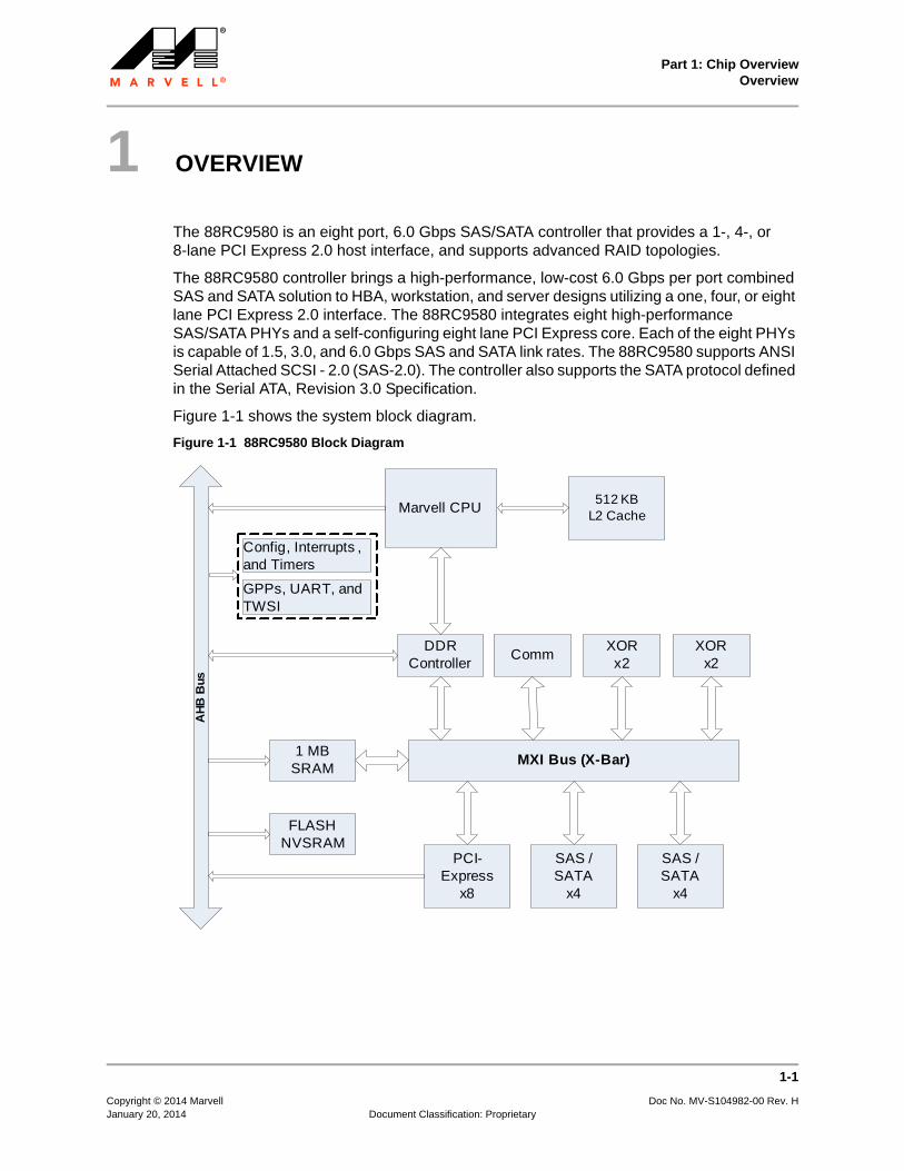
The 88RC9580 is an eight port, 6.0 Gbps SAS/SATA controller that provides a 1-, 4-, or 8-lane PCI Express 2.0 host interface, and supports advanced RAID topologies.
The 88RC9580 controller brings a high-performance, low-cost 6.0 Gbps per port combined SAS and SATA solution to HBA, workstation, and server designs utilizing a one, four, or eight lane PCI Express 2.0 interface. The 88RC9580 integrates eight high-performance SAS/SATA PHYs and a self-configuring eight lane PCI Express core. Each of the eight PHYs is capable of 1.5, 3.0, and 6.0 Gbps SAS and SATA link rates. The 88RC9580 supports ANSI Serial Attached SCSI - 2.0 (SAS-2.0). The controller also supports the SATA protocol defined in the Serial ATA, Revision 3.0 Specification.
Figure 1-1 shows the system block diagram.
Figure 1-1 88RC9580 Block Diagram
AH
B B
us
MXI Bus (X-Bar)
DDR Controller
PCI-Express
x8
CommXORx2
FLASHNVSRAM
Marvell CPU
XORx2
1 MBSRAM
512 KBL2 Cache
SAS / SATA
x4
SAS / SATA
x4
Config, Interrupts , and Timers
GPPs, UART, andTWSI

THIS PAGE LEFT INTENTIONALLY BLANK
88RC9580 R2.3 Eight-Lane PCIe 2.0 to Eight-Port SAS/SATA 6 Gbps RAID-on-Chip Processor Preliminary Datasheet
1-2
Copyright © 2014 Marvell Doc No. MV-S104982-00 Rev. HJanuary 20, 2014 Document Classification: Proprietary

Part 1: Chip OverviewFeatures
2-1
Copyright © 2014 Marvell Doc No. MV-S104982-00 Rev. HJanuary 20, 2014 Document Classification: Proprietary
2 FEATURES
The chapter contains the following sections:
General
Embedded CPU
DDR Controller
PCI Express
SAS (Direct Attach or Expander)
SATA (Direct Attach)
XOR Engine

88RC9580 R2.3 Eight-Lane PCIe 2.0 to Eight-Port SAS/SATA 6 Gbps RAID-on-Chip Processor Preliminary Datasheet
2-2 General
Copyright © 2014 Marvell Doc No. MV-S104982-00 Rev. HJanuary 20, 2014 Document Classification: Proprietary
2.1 General
Eight SAS/SATA ports.
Choice of x1, x2, x4 lane PCIe 2.0 host interface.
Embedded CPU for full RAID off load.
Supports I2O and Marvell Universal Messaging Interface (UMI).
Supports three Serial Device Bus (I2C) controllers for communicating with hardware monitoring ICs.
Supports two industry standard 57600 UARTs.
Supports two SFF-8485 compliant SGPIO ports.
Supports autodetection of SAS or native SATA device.
Up to 4096 concurrent I/O operations (2048 per 4 ports).
Up to 128 concurrent SATA Devices (64 per 4 ports).
No limit on the number of devices supported.
55 nm CMOS process, 1.0V digital core, 2.5V/1.8V analog power supply, 1.5V/1.8V DDR I/O, and 3.3V I/O supply.
Estimated power (4-port): 8W.
Estimated power (8-port): 9W.
Up to 42 LED/GPIO ports.
Supports hardware RAID 5 and RAID 6 acceleration.
Supports Data Path Parity Protection (DPP).

Part 1: Chip OverviewFeatures
Embedded CPU 2-3
Copyright © 2014 Marvell Doc No. MV-S104982-00 Rev. HJanuary 20, 2014 Document Classification: Proprietary
2.2 Embedded CPU
Embedded 800 MHz Marvell 88SV581 V6 CPU core.
Compliant with ARM v6 Architecture.
Integrated 32 KB L1 ICache.
Integrated 32 KB L1 DCache.
Integrated 512 KB L2 Cache.
Integrated 1 MB dual port SRAM (AHB bus and MXI bus).
Supports up to 4 MB of external NVSRAM memory (x8 / x16).
Supports up to 4 MB of external PBSRAM memory (x32).
Supports up to 8 MB of external Parallel Flash memory (x8 / x16).
The CPU can be disabled for ultra low power applications. (Driver can run in host memory).

88RC9580 R2.3 Eight-Lane PCIe 2.0 to Eight-Port SAS/SATA 6 Gbps RAID-on-Chip Processor Preliminary Datasheet
2-4 DDR Controller
Copyright © 2014 Marvell Doc No. MV-S104982-00 Rev. HJanuary 20, 2014 Document Classification: Proprietary
2.3 DDR Controller
2.3.1 Supported System Features
One Memory Controller port connected to the CPU, and four ports connected to the MXI bus.
Byte Enable (BE) strobe to write individual byte locations within any burst.
Supports burst length up to 8 cycles. MCB can support burst length up to 16 (AXI compatible).
A burst can start on any address aligned to its word size. 64-bit bursts can burst from any 64-bit-aligned address).
Support for CPU to perform critical-word-first, 32-Byte cacheline read.
2.3.2 Supported SDRAM Features
Supports DDR2 and DDR3 devices.
Supports 16 address pins. Supports all ranges of DRAM sizes from 64 Mb and up.
Supports UDIMM.
2.3.3 Supported SDRAM Functions
Supports up to three chip selects (CS) and up to eight banks per CS.
Each CS has an independent bank, row, and column address.
Each CS can be mapped to a different starting address.
Each CS can be programmed for 8 MB to 4 GB.
DRAM banks are left open after access unless auto-precharge is enabled.
Supports Auto-precharge. Only the last burst in a contiguous access is issued with auto-precharge.
Supports two bank interleave operation. When one bank is pending timer expiration, another bank can perform precharge and active, but data transfer is always in order.
Supports deep data pipeline for high bandwidth utilization.
Supports burst length of 2, 4, and 8 for the applicable DDR type.
(DDR2,3) Flexible configuration for PAD termination and SDRAM ODT switching logic
Programmable address order:
Fast-bank order: Address = CS, Row, Bank, Column, Data-width.
Regular order: Address = CS, Bank, Row, Column, Data-width (default).
Supports all CAS values up to the maximum Memory Controller frequency.
Supports power-saving features (active/precharge power down, self-refresh). These can be controlled automatically after an idle timer expires, issued manually by writing to registers, or controlled with dedicated external ports.
Supports up to seven posted-auto-refreshes when idle, providing more effective bandwidth.
E/MRS commands can be manually issued after updating the corresponding register values.

Part 1: Chip OverviewFeatures
DDR Controller 2-5
Copyright © 2014 Marvell Doc No. MV-S104982-00 Rev. HJanuary 20, 2014 Document Classification: Proprietary
2.3.4 DDR Memory Controller Special Features
Test mode provides full control over address/command bus (no data control).
Programmable pad calibration and driving strength control.

88RC9580 R2.3 Eight-Lane PCIe 2.0 to Eight-Port SAS/SATA 6 Gbps RAID-on-Chip Processor Preliminary Datasheet
2-6 PCI Express
Copyright © 2014 Marvell Doc No. MV-S104982-00 Rev. HJanuary 20, 2014 Document Classification: Proprietary
2.4 PCI Express
Supports x1, x2, x4 lane PCIe 2.0 Interface (5.0 Gbps).
Supports four fully independent PCIe functions.
Supports independent communication, message, doorbell, and interrupt mechanisms for each PCIe function.
Supports Message Signal Interrupts (MSI).
All registers memory mapped.
Supports PCIe Power Management: D0, D1, D3COLD, D3HOT.
Internal registers and memory can be made visible or invisible to PCIe functions.
Supports independent I2O interface for each PCIe function.
Supports independent Marvell Universal Messaging Interface (UMI) for each PCIe function.

Part 1: Chip OverviewFeatures
SAS (Direct Attach or Expander) 2-7
Copyright © 2014 Marvell Doc No. MV-S104982-00 Rev. HJanuary 20, 2014 Document Classification: Proprietary
2.5 SAS (Direct Attach or Expander)
Serial Attached SCSI (SAS-2.0) compliant.
Supports 6 Gbps, 3 Gbps, and 1.5 Gbps devices.
Supports SAS Multiplexing. Up to 16 logical ports when multiplexing is enabled on all PHYs.
Supports SSC, with independent control for each PHY using SSC_EN (R060h [17]).
Supports wide SAS ports. Up to four wide when multiplexing is disabled, and up to eight wide when multiplexing is enabled.
Supports Serial SCSI Protocol (SSP), initiator and target mode.
Supports SAS Management Protocol (SMP), initiator mode.
Supports Serial ATA Tunneling Protocol (STP), initiator mode.
Non-zero offset and non-sequential data delivery.
ATA and ATAPI commands.
Native Command Queuing (NCQ).
Supports T10 Protection Information Model. DIF fields can be inserted, checked, replaced, and/or removed.
Supports Transport Layer Retries.
Supports hardware assisted Scatter-Gather.

88RC9580 R2.3 Eight-Lane PCIe 2.0 to Eight-Port SAS/SATA 6 Gbps RAID-on-Chip Processor Preliminary Datasheet
2-8 SATA (Direct Attach)
Copyright © 2014 Marvell Doc No. MV-S104982-00 Rev. HJanuary 20, 2014 Document Classification: Proprietary
2.6 SATA (Direct Attach)
Serial ATA Revision 3.0 (6 Gbps) compliant, with speed negotiation to 3.0 Gbps and 1.5 Gbps.
Supports programmable SATA signaling levels, including Gen1x, Gen2i, and Gen2x.
Supports ATA and ATAPI commands.
Supports Native Command Queuing (NCQ).
Non-zero offset and non-sequential data delivery.
32 outstanding commands per device.
Supports Port Multiplier.
FIS based Switching on NCQ and legacy commands.
Supports Host mode and Device mode of operation.
Supports hardware assisted Scatter-Gather.

Part 1: Chip OverviewFeatures
XOR Engine 2-9
Copyright © 2014 Marvell Doc No. MV-S104982-00 Rev. HJanuary 20, 2014 Document Classification: Proprietary
2.7 XOR Engine
Supports Advanced RAID features including:
Dual XOR RAID 6.
P + Q + Copy, or Q + Q + Q RAID 6.
Memory Block Fill.
Zero Result Check.
Generates up to 3 checksums concurrently, including any combination of P and Q.
Independent GF Multiply coefficient for each of 3 concurrent Q checksum calculations.
Supports rebuilding three failed drives simultaneously with a single read of remaining good drives.
Supports chained XOR Descriptor Tables, with up to 32 operations in each table.
Supports Scatter-Gather transfers using a common PRD format.
Supports CRC32 checksum generation and checking.

THIS PAGE LEFT INTENTIONALLY BLANK
88RC9580 R2.3 Eight-Lane PCIe 2.0 to Eight-Port SAS/SATA 6 Gbps RAID-on-Chip Processor Preliminary Datasheet
2-10 XOR Engine
Copyright © 2014 Marvell Doc No. MV-S104982-00 Rev. HJanuary 20, 2014 Document Classification: Proprietary

Part 1: Chip OverviewPackage
3-1
Copyright © 2014 Marvell Doc No. MV-S104982-00 Rev. HJanuary 20, 2014 Document Classification: Proprietary
3 PACKAGE
This chapter contains the following sections:
Ball Diagram
Mechanical Dimensions
Signal Descriptions

88RC9580 R2.3 Eight-Lane PCIe 2.0 to Eight-Port SAS/SATA 6 Gbps RAID-on-Chip Processor Preliminary Datasheet
3-2 Ball Diagram
Copyright © 2014 Marvell Doc No. MV-S104982-00 Rev. HJanuary 20, 2014 Document Classification: Proprietary
3.1 Ball Diagram
The 676-pin FCBGA ball diagram is illustrated in Figure 3-1.
Figure 3-1 88RC9580 Ball Diagram
VSSSDRAM_
DQM[1]SDRAM_
DQ[11]
SDRAM_
DQ[8] SDRAM_
DQ[6] VSSSDRAM_
DQS[0] SDRAM_
DQSB[0]SDRAM_
DQ[0] VSSPRXN[7]
VSSPRXN[6]
VSSPRXP[4]
VSSPTXP[3]
VSSPRXP[3]
VSSPRXP[2]
VSSPTXP[0]
VSSPIN_TEST
[13] VSS
SDRAM_
DQSB[1]SDRAM_
DQS[1] SDRAM_
DQ[12]
VDDQSDRAM_
DQ[9] SDRAM_
DQ [7] SDRAM_
DQ[5] VDDQSDRAM_
DQ[2] VSSPRXP[7]
VSSPRXP[6]
VSSPRXN[4]
VSSPTXN[3]
VSSPRXN[3]
VSSPRXN[2]
VSSPTXN[0]
VSSPIN_G
PIO
[5] PIN_GPIO
[1]
SDRAM_
DQ[14]
VSSSDRAM_
DQ[15]
SDRAM_
DQ[13]
SDRAM_
DQ[10]
VSSSDRAM_
DQ[3] SDRAM_
DQ[4] SDRAM_
DQ[1] SDRAM_
DQM[0] VSSPTXN[6]
VSSPRXP[5]
VSSREFCLK
NVSS
PTXN[2]VSS
PRXP[1]VSS
PTPVSS
PIN_GPIO
[0] PIN_TEST
[14]
PIN_TEST
[12]
SDRAM_
DQ[25]
SDRAM_
DQM[3]SDRAM_
DQ[20]
VDDQSDRAM_
DQ[16]
SDRAM_
DQ[19]
SDRAM_
DQM[2]VDDQ
VREFSSDRAM_
CAL_PAD
VSSPTXP[6]
VSSPRXN[5]
VSSREFCLK
PVSS
PTXP[2]VSS
PRXN[1]VSS
PIN_ISET
AVDD25_1
PIN_GPIO
[2] PIN_GPIO
[6] PIN_TEST
[11]
SDRAM_
DQ[27]
VSSSDRAM_
DQSB[2]SDRAM_
DQS[2]SDRAM_
DQ[22]
VSSSDRAM_
DQ[21]
SDRAM_
DQ[17]
SDRAM_
RESETNVSS
PTXN[7]VSS
PTXP[5]VSS
PTXN[4]VSS
PTXP[1]VSS
PRXN[0]VSS
PIN_BBU_
REQPIN_TEST
[10]
PIN_TEST
[15]
PIN_TEST
[9] PIN_TEST
[8] PIN_TEST
[7]
SDRAM_
DQSB[3]SDRAM_
DQS[3]SDRAM_
DQ[26]
VDDQSDRAM_
DQ[24]
SDRAM_
DQ[18]
SDRAM_
DQ[23]
VDDQVREFD
VSSPTXP[7]
VSSPTXN[5]
VSSPTXP[4]
VSSPTXN[1]
VSSPRXP[0]
VSSPIN_G
PIO
[3] PIN_TEST
[4] PIN_TEST
[3] PIN_TEST
[6] PIN_TEST
[0] PIN_FLT
[8]
SDRAM_
DQ[31]
VSSSDRAM_
DQ[30]
SDRAM_
DQ[28]
SDRAM_
DQ[29]
VSSVDDQ
VSSVSS
AVDD25_0
AVDD[4-7_8]
AVDD[4-7_8]
AVDD[4-7_8]
HSDACNVSS
AVDD[0-3_8]
AVDD[0-3_8]
AVDD[0-3_8]
VSSPIN_G
PIO
[4] PIN_TEST
[1] PIN_FLT
[7] PIN_FLT
[6] PIN_FLT
[0] PIN_FLT
[3] PIN_FLT
[4]
SDRAM_
CLKN[0]
SDRAM_
CLK[0] SDRAM_
ODT1VDDQ
SDRAM_
CKE0 SDRAM_
CSN0VDDQ
VSSVSS
AVDD[4-
7_8]
AVDD[4-7_8]
AVDD[4-7_8]
AVDD[4-7_8]
HSDACP
AVDD[0-3_8]
AVDD[0-3_8]
AVDD[0-3_8]
AVDD[0-3_8]
PIN_GPIO
[7] PIN_TEST
[2] PIN_FLT
[1] PIN_FLT
[2] PIN_ACT
[7] PIN_FLT
[5] PIN_ACT
[4] PIN_ACT
[0]
SDRAM_
CASN VSSSDRAM_
CSN1SDRAM_
ODT0SDRAM_
CSN2VSS
VDDQVSS
VSSVSS
VSSVSS
VSSVSS
VSSVSS
VSSVDDO1
PIN_TEST
[5] PIN_ACT
[8] PIN_ACT
[1] PIN_ACT
[5] PIN_ACT
[2] PIN_SCL
[2] PIN_SDA
[1] PIN_SCL
[1]
SDRAM_
WEN SDRAM_
CLKN[2]
SDRAM_
CLK[2]
VDDQSDRAM_
ODT2SDRAM_
RASNVDDQ
VSSVDD
VSSVDD
VSSVDD
VSSVDD
VSSVDD
VDDO1PIN_A
CT
[6] PIN_ACT
[3] PIN_SDA
[2] PIN_UAI
[1] PIN_UAI
[0] PIN_TDI
PIN_TMS
PIN_SDA[0]
AVDD_DDR
VSSSDRAM_
BA[1] SDRAM_
BA[2]SDRAM_
BA[0] VSSVDDQ
VSSVSS
VDDVSS
VDDVSS
VDDVSS
VDDVSS
VDDO1PIN_S
CL
[0] PIN_UAO
[0] PIN_UAO
[1] PIN_TCKPIN_F_
OE_N PIN_F_
CE_N PIN_F_
WE_N PIN_F_
RESET
_N
SDRAM_
ADDR[5]SDRAM_
ADDR[3]SDRAM_
ADDR[2]VDDQ
SDRAM_
ADDR[1]SDRAM_
ADDR[0]VDDQ
VSSVDD
VSSVDD
VSSVDD
VSSVDD
VSSVDD
VDDO1
PIN_TDO
PIN_N_O
E_N
PIN_N_
CE_N PIN_F_
READYPIN_F_
BYTE_N PIN_P_
DATA[34
] PIN_N_
WE_N PIN_P_
DATA[16
]
SDRAM_
CKE1 VSSSDRAM_
ADDR[4]SDRAM_
ADDR[6]SDRAM_
ADDR[7]VSS
VDDQVSS
VSSVDD
VSSVDD
VSSVDD
VSSVDD
VSSVDDO1 PIN_P
_
DATA[22
] PIN_P_
DATA[24
] PIN_P_
DATA[23
] PIN_P_
DATA[21
] PIN_P_
DATA[20
] PIN_P_
DATA[19
] PIN_P_
DATA[18
] PIN_P_
DATA[17
]
SDRAM_
CLK[1] SDRAM_
CLKN[1]
SDRAM_CKE2
VDDQSDRAM_
ADDR[8]SDRAM_
ADDR[9]VDDQ
VSSVDD
VSSVDD
VSSVDD
VSSVDD
VSSVDD
VDDO1VDDO1
PIN_P_
DATA[30
] PIN_P_
DATA[27
] PIN_P_
DATA[31
] PIN_P_
DATA[28
] PIN_P_
DATA[29
] PIN_P_
DATA[26
] PIN_P_
DATA[25
]
SDRAM_
ADDR[10]
VSSSDRAM_
ADDR[11]SDRAM_
ADDR[12]
SDRAM_
ADDR[13]
VSSVDDQ
VSSVSS
VDDVSS
VDDVSS
VDDVSS
VDDVSS
VDDO1PIN_P
_
DATA[3]
PIN_P_
ADDR[12
]PIN_P
_
ADDR[4]
PIN_P_
ADDR[5]
PIN_P_
DATA[35
] PIN_P_
ADDR[19
] PIN_P_
ADDR[3]
PIN_P_
ADDR[2]
SDRAM_
ADDR[15]SDRAM_
ADDR[14]SDRAM_
CB[0] VDDQSDRAM_
CBM SDRAM_
CB[5] VDDQVSS
VDDVSS
VDDVSS
VDDVSS
VDDVSS
VDDVDDO1 PIN_P
_
DATA[12
] PIN_P_
DATA[4]
PIN_P_
ADDR[11
] PIN_P_
ADDR[18
] PIN_P_
ADDR[17
] PIN_P_
ADDR[10
]
PIN_P_
ADDR[16
]
PIN_P_
ADDR[0]
SDRAM_
CB[2] SDRAM_
CBSB VSSSDRAM_
CB[1] SDRAM_
CB[4] VSSVDDQ
VSSVSS
VDDVSS
VDDVSS
VDDVSS
VDDVSS
VDDO1
PIN_P_O
UT_
CLK PIN_P_
ADV_N PIN_P_
DATA[6]
PIN_P_
ADDR[13
] PIN_P_
ADDR[14
]
PIN_P_
ADDR[1]
PIN_P_
ADDR[15
] PIN_P_
DATA[1]
SDRAM_
DQM[4]SDRAM_
CBS SDRAM_
CB[3] VDDQSDRAM_
CB[7] SDRAM_
CB[6] VDDQVSS
VDDVSS
VDDVSS
VDDVSS
VDDVSS
VDDVDDO1
PIN_RESET
_NPIN_P
_
WE_N[2]
PIN_P_
DATA[33
]PIN_P
_
DATA[5]
PIN_P_
DATA[32
] PIN_P_
DATA[0]
PIN_P_
DATA[2]
PIN_P_
DATA[7]
SDRAM_
DQ[32]
VSS SDRAM_
DQ[33]
SDRAM_
DQ[35]
SDRAM_
DQ[34]
VSSVDDQ
VSSVSS
VSSVSS
VSSVSS
VSSVSS
VSSVSS
VDDO1 PIN_F
_TEST[2]
PIN_P_
ADDR[21
] PIN_P_
WE_N[0]
PIN_P_
ADDR[9]
PIN_P_
DATA[8]
PIN_P_
DATA[9]
PIN_P_
DATA[10
] PIN_P_
DATA[11
]
SDRAM_
DQSB[4]SDRAM_
DQS[4]
SDRAM_DQ[38
]
VDDQSDRAM_
DQ[36]
SDRAM_
DQ[39]
VDDQVSS
VAA[0-3]
VAA[0-3]
VAA[0-3]
VAA[0-3]
VAA[0-3]
VAA[0-3]
VAA[4-7]
VAA[4-7]
VAA[4-7]
VAA[4-7]
VAA_ANA
PIN_M_D
ATA
PIN_SPI_
CS_N PIN_P_
ADDR[6]
PIN_P_
ADDR[8]
PIN_P_
DATA[15
] PIN_P_
DATA[13
] PIN_P
_
DATA[14
]
SDRAM_
DQ[37]
VSSSDRAM_
DQ[40]
SDRAM_
DQM[5] SDRAM_
DQ[41]
VSSSDRAM_
DQ[57]
SDRAM_
DQ[60]
VAA[0-3]
VSSPIN_TXN
[1] VSSPIN_TXN
[3] VSSVAA[4-7
]VSS
PIN_TXN
[5] VSSVAA[4-7
]
VAA_PLL
PIN_M_C
LKPIN_P
_
ADDR[22
] PIN_P_
CS1_N PIN_P_
ADSC_N
PIN_P_
GW_N
PIN_P_B
W_N
SDRAM_
DQSB[5]SDRAM_
DQS[5] SDRAM_
DQ[42]
VDDQSDRAM_
DQ[46]
SDRAM_
DQM[7]SDRAM_
DQ[56]
VDDQVAA[0-3
]VSS
PIN_TXP
[1] VSSPIN_TXP
[3] VSSVAA[4-7
]VSS
PIN_TXP
[5] VSSVAA[4-7
]VSS
ISETVHV PIN_P
_
ADDR[20
] PIN_P_
ADDR[23
] PIN_P_
WE_N[3]
PIN_P_O
E_N
SDRAM_
DQ[43]
VSSSDRAM_
DQ[45]
SDRAM_
DQ[44]
SDRAM_
DQ[47]
VSSSDRAM_
DQ[59]
SDRAM_
DQ[63]
VSSPIN_TXN
[0] VSSPIN_TXN
[2] VSSPIN_R
XP
[3] VSSPIN_TXN
[4] VSSPIN_TXN
[6] VSSPIN_TXP
[7] VSS PIN_F_
TEST[0] PIN_S
PI_
CLKPIN_S
PI_DO
PIN_P_
ADDR[7] PIN_S
PI_DI
SDRAM_
DQ[48]
SDRAM_
DQM[6] SDRAM_
DQ[49]
VDDQSDRAM_
DQ[55]
SDRAM_
DQ[58]
SDRAM_
DQ[61]
VDDQVSS
PIN_TXP
[0] VSSPIN_TXP
[2] VSSPIN_R
XN
[3] VSSPIN_TXP
[4] VSSPIN_TXP
[6] VSSPIN_TXN
[7] VSS PIN_F_
TEST[3]
PIN_F_
TEST[4] PIN_C
NFG
[1] PIN_PRE
SET_N PIN_P_
WE_N[1]
SDRAM_
DQ[50]
VSSSDRAM_
DQ[51]
SDRAM_
DQ[52]
SDRAM_
DQ[53]
VSSSDRAM_
DQ[62]
VSSPIN_R
XP
[0] VSSPIN_R
XN
[1] VSSPIN_R
XN
[2] VSSPIN_R
XN
[4] VSSPIN_R
XN
[5] VSSPIN_R
XN
[6] VSSPIN_R
XN
[7] VSS
PIN_NSRST
PIN_NTRST
PIN_F_
TEST[1]
PIN_CNFG
[0]
VSS SDRAM_
DQS[6]SDRAM_
DQSB[6]VDDQ
SDRAM_
DQ[54]
SDRAM_
DQSB[7]SDRAM_
DQS[7] VSSPIN_R
XN
[0] VSSPIN_R
XP
[1] VSSPIN_R
XP
[2] VSSPIN_R
XP
[4] VSSPIN_R
XP
[5] VSSPIN_R
XP
[6] VSSPIN_R
XP
[7] VSSPIN_TP
PIN_REFCLK
PIN_F_
TEST[5] VSS

Part 1: Chip OverviewPackage
Mechanical Dimensions 3-3
Copyright © 2014 Marvell Doc No. MV-S104982-00 Rev. HJanuary 20, 2014 Document Classification: Proprietary
3.2 Mechanical Dimensions
The package mechanical drawing is shown in Figure 3-2 and the mechanical dimensions are shown in Figure 3-3.
Figure 3-2 Package Mechanical Drawing

88RC9580 R2.3 Eight-Lane PCIe 2.0 to Eight-Port SAS/SATA 6 Gbps RAID-on-Chip Processor Preliminary Datasheet
3-4 Mechanical Dimensions
Copyright © 2014 Marvell Doc No. MV-S104982-00 Rev. HJanuary 20, 2014 Document Classification: Proprietary
Figure 3-3 Package Mechanical Dimensions

Part 1: Chip OverviewPackage
Signal Descriptions 3-5
Copyright © 2014 Marvell Doc No. MV-S104982-00 Rev. HJanuary 20, 2014 Document Classification: Proprietary
3.3 Signal Descriptions
This section includes information on signal definitions and descriptions.
3.3.1 Signal Definitions
Signal type definitions are shown in Table 3-1.
3.3.2 Signal Descriptions
This section outlines the 88RC9580 signal descriptions. Signals ending with the letter N are active-low signals.
Table 3-1 Signal Type Definitions
Signal Type Definition
I/O Input and output
I Input only
O Output only
OC Open Collector
OD Open-Drain pad
Table 3-2 General Purpose I/O Signals
Signal NameSignal Number
Type Description
PIN_ACT[8]
PIN_ACT[7]
PIN_ACT[6]
PIN_ACT[5]
PIN_ACT[4]
PIN_ACT[3]
PIN_ACT[2]
PIN_ACT[1]
PIN_ACT[0]
J20
H23
K19
J22
H25
K20
J23
J21
H26
I/O, OC Activity LED.
Active low.
PIN_ACT is active when SAS/SATA PHY is transmitting or receiving.
These pins can be used as GPIO.
PIN_ACT[7:0]: SAS/SATA PHY[7:0] activity.
PIN_ACT[8]: Global Activity. Enabled when any SAS/SATA PHY is active.
PIN_BBU_REQ E21 I Battery backup request.

88RC9580 R2.3 Eight-Lane PCIe 2.0 to Eight-Port SAS/SATA 6 Gbps RAID-on-Chip Processor Preliminary Datasheet
3-6 Signal Descriptions
Copyright © 2014 Marvell Doc No. MV-S104982-00 Rev. HJanuary 20, 2014 Document Classification: Proprietary
PIN_FLT[8]
PIN_FLT[7]
PIN_FLT[6]
PIN_FLT[5]
PIN_FLT[4]
PIN_FLT[3]
PIN_FLT[2]
PIN_FLT[1]
PIN_FLT[0]
F26
G22
G23
H24
G26
G25
H22
H21
G24
I/O, OC Fault LED.
Active low signals.
PIN_FLT is active when PHY is not ready or when PHY is ready and there is any PHY related error or connection error.
These pins can be used as GPIO, SGPIO, I2C, or FLT_LED. See GPIO_FLT_CFG (R10080h [7:0]) and I2C_SGPIO_FLT_PAD_SEL (R10104h [9:8]).
Pins used as Fault LED:
PIN_FLT[8]: Global Fault indication. The indicator is on when any SAS/SATA_PHY has a fault.
PIN_FLT[7:0] corresponds to SAS/SATA_PHY7 through PHY0.
When PHY is not ready, PIN_FLT[7:0] is always on. After the PHY is ready, a fault occurs.
Pins used as SGPIO:
PIN_FLT[8]: Same as FLT mode.
PIN_FLT[7:4]: SGPIO1 SCLK, SLOAD, SDOUT, SDIN
PIN_FLT[3:0]: SGPIO0 SCLK, SLOAD, SDOUT, SDIN
Used as I2C:
PIN_FLT[8]: Same as FLT Mode
PIN_FLT[7:6]: I2C2 CLK, DATA
PIN_FLT[5:4]: Not used
PIN_FLT[3:2]: I2C1 CLK, DATA
PIN_FLT[1:0]: Not used
Table 3-2 General Purpose I/O Signals (continued)
Signal NameSignal Number
Type Description

Part 1: Chip OverviewPackage
Signal Descriptions 3-7
Copyright © 2014 Marvell Doc No. MV-S104982-00 Rev. HJanuary 20, 2014 Document Classification: Proprietary
PIN_GPIO[7]
PIN_GPIO[6]
PIN_GPIO[5]
PIN_GPIO[4]
PIN_GPIO[3]
PIN_GPIO[2]
PIN_GPIO[1]
PIN_GPIO[0]
H19
D25
B25
G20
F21
D24
B26
C24
I/O General Purpose I/O.
Table 3-2 General Purpose I/O Signals (continued)
Signal NameSignal Number
Type Description

88RC9580 R2.3 Eight-Lane PCIe 2.0 to Eight-Port SAS/SATA 6 Gbps RAID-on-Chip Processor Preliminary Datasheet
3-8 Signal Descriptions
Copyright © 2014 Marvell Doc No. MV-S104982-00 Rev. HJanuary 20, 2014 Document Classification: Proprietary
PIN_TEST[15]
PIN_TEST[14]
PIN_TEST[13]
PIN_TEST[12]
PIN_TEST[11]
PIN_TEST[10]
PIN_TEST[9]
PIN_TEST[8]
PIN_TEST[7]
PIN_TEST[6]
PIN_TEST[5]
PIN_TEST[4]
PIN_TEST[3]
PIN_TEST[2]
PIN_TEST[1]
PIN_TEST[0]
E23
C25
A25
C26
D26
E22
E24
E25
E26
F24
J19
F22
F23
H20
G21
F25
I/O Configuration and test pins. These pins can be used as GPIO.
PIN_TEST[15]–PCIe power-up disable
0: Enable PCIe after power-up1: Disable PCIe after power-up
PIN_TEST[14:13]–Chip reference clock selection
0h: 20 MHz1h: 50 MHz2h: 100 MHz3h: 75 MHz
PIN_TEST[12]–CPU VINITH
0: Boot from 00000000h1: Boot from FFFF0000h
PIN_TEST[11:10]–Boot mode
0h: Boot from 00000000h or FFFF0000h, depending on the value of VINITH.
1h: When VINITH is 1h, boot from SPI.2h: When VINITH is 1h, boot from Parallel Flash.3h: When VINITH is 1h, boot from Scratchpad.
PIN_TEST[10]–PCIE ROM location if CPU is disabled
0: Parallel Flash1: Serial Flash
PIN_TEST[9:8]–Reserved, must be 3h or 0h.
PIN_TEST[7]– CPU enable.
0: Disable CPU1: Enable CPU
PIN_TEST[6]–DRAM enable.
0: Disable DRAM1: Enable DRAM
PIN_TEST[5]–PCIe configuration access enable
0: PCIe responds to configuration access1: PCIe returns a retry configuration access
PIN_TEST[4]–Parallel Flash x8/x16
0: Byte mode1: Word mode
PIN_TEST[3:2]–Internal CPU/DDR speed
0h: CPU 800 MHz, DDR 400 MHz1h: CPU 1000 MHz, DDR 500 MHz2h: CPU 1200 MHz, DDR 600 MHz3h: CPU 600 MHz, DDR 300 MHz
PIN_TEST[1]–UART baud rate
0: 576001: Reserved
PIN_TEST[0]–UART mode
0: Reserved1: Terminal mode
Table 3-2 General Purpose I/O Signals (continued)
Signal NameSignal Number
Type Description

Part 1: Chip OverviewPackage
Signal Descriptions 3-9
Copyright © 2014 Marvell Doc No. MV-S104982-00 Rev. HJanuary 20, 2014 Document Classification: Proprietary
Table 3-3 Clock and Reset Signals
Signal NameSignal Number
Type Description
PIN_REFCLK AF24 I Reference clock input, CMOS level.
2.5V, ± 350 ppm.
The signal level on this pin shall not exceed the max of VAA1OP.
PIN_RESET_N V19 I Power-on reset.
PIN_PRESET_N AD25 I PCIe Reset
PIN_TP AF23 O SAS/SATA analog test port.
Table 3-4 I2C Signals
Signal NameSignal Number
Type Description
PIN_SCL[2]
PIN_SCL[1]
PIN_SCL[0]
J24
J26
L19
I/O, OC I2C clock.
PIN_SDA[2]
PIN_SDA[1]
PIN_SDA[0]
K21
J25
K26
I/O, OC I2C data.
Table 3-5 JTAG Signals
Signal NameSignal Number
Type Description
PIN_NSRST AE23 I JTAG system reset, active low.
PIN_NTRST AE24 I JTAG test reset, active low.
PIN_TCK L22 I JTAG clock.
PIN_TDI K24 I JTAG data input.
PIN_TDO M19 I JTAG data output.
PIN_TMS K25 I JTAG test mode select.
Table 3-6 UART Signals
Signal NameSignal Number
Type Description
PIN_UAI[1]
PIN_UAI[0]
K22
K23
I UART input.
PIN_UAO[1]
PIN_UAO[0]
L21
L20
O UART output.

88RC9580 R2.3 Eight-Lane PCIe 2.0 to Eight-Port SAS/SATA 6 Gbps RAID-on-Chip Processor Preliminary Datasheet
3-10 Signal Descriptions
Copyright © 2014 Marvell Doc No. MV-S104982-00 Rev. HJanuary 20, 2014 Document Classification: Proprietary
.
Table 3-7 Parallel Flash Signals
Signal NameSignal Number
Type Description
PIN_F_BYTE_N M23 O Parallel flash byte mode.
PIN_F_CE_N L24 O Parallel flash chip select.
PIN_F_OE_N L23 O Parallel flash output enable.
PIN_F_READY M22 I Parallel flash ready signal.
Requires external pull-up resistor.
PIN_F_RESET_N L26 O Parallel flash reset.
PIN_F_WE_N L25 O Parallel flash write enable.

Part 1: Chip OverviewPackage
Signal Descriptions 3-11
Copyright © 2014 Marvell Doc No. MV-S104982-00 Rev. HJanuary 20, 2014 Document Classification: Proprietary
PIN_P_ADDR[23]
PIN_P_ADDR[22]
PIN_P_ADDR[21]
PIN_P_ADDR[20]
PIN_P_ADDR[19]
PIN_P_ADDR[18]
PIN_P_ADDR[17]
PIN_P_ADDR[16]
PIN_P_ADDR[15]
PIN_P_ADDR[14]
PIN_P_ADDR[13]
PIN_P_ADDR[12]
PIN_P_ADDR[11]
PIN_P_ADDR[10]
PIN_P_ADDR[9]
PIN_P_ADDR[8]
PIN_P_ADDR[7]
PIN_P_ADDR[6]
PIN_P_ADDR[5]
PIN_P_ADDR[4]
PIN_P_ADDR[3]
PIN_P_ADDR[2]
PIN_P_ADDR[1]]
PIN_P_ADDR[0]
AB24
AA22
W20
AB23
R24
T22
T23
U24
U25
U23
U22
R20
T21
T24
W22
Y23
AC25
Y22
R22
R21
R25
R26
T25
T26
O Shared address bus for parallel flash, NVSRAM and PBSRAM
For Parallel Flash: Signals are Word addresses.
For NVSRAM: Signals are Word addresses.
For PBSRAM: Signals are Dword addresses.
Table 3-7 Parallel Flash Signals (continued)
Signal NameSignal Number
Type Description

88RC9580 R2.3 Eight-Lane PCIe 2.0 to Eight-Port SAS/SATA 6 Gbps RAID-on-Chip Processor Preliminary Datasheet
3-12 Signal Descriptions
Copyright © 2014 Marvell Doc No. MV-S104982-00 Rev. HJanuary 20, 2014 Document Classification: Proprietary
PIN_P_DATA[35]
PIN_P_DATA[34]
PIN_P_DATA[33]
PIN_P_DATA[32]
PIN_P_DATA[31]
PIN_P_DATA[30]
PIN_P_DATA[29]
PIN_P_DATA[28]
PIN_P_DATA[27]
PIN_P_DATA[26]
PIN_P_DATA[25]
PIN_P_DATA[24]
PIN_P_DATA[23]
PIN_P_DATA[22]
PIN_P_DATA[21]
PIN_P_DATA[20]
PIN_P_DATA[19]
PIN_P_DATA[18]
PIN_P_DATA[17]
PIN_P_DATA[16]
PIN_P_DATA[15]
PIN_P_DATA[14]
PIN_P_DATA[13]
PIN_P_DATA[12]
PIN_P_DATA[11]
PIN_P_DATA[10]
PIN_P_DATA[9]
PIN_P_DATA[8]
PIN_P_DATA[7]
PIN_P_DATA[6]
PIN_P_DATA[5]
PIN_P_DATA[4]
PIN_P_DATA[3]
PIN_P_DATA[2]
PIN_P_DATA[1]
PIN_P_DATA[0]
R23
M24
V21
V23
P22
P20
P24
P23
P21
P25
P26
N20
N21
N19
N22
N23
N24
N25
N26
M26
Y24
Y26
Y25
T19
W26
W25
W24
W23
V26
U21
V22
T20
R19
V25
U26
V24
I/O Shared Data Bus for Parallel Flash/NVSRAM/PBSRAM
For Parallel Flash: DATA[15:0] are used.
In Byte Mode: DATA[15] is Address bit 0. DATA[7:0] are data.
In Word Mode: DATA[15:0] are data.
For NVSRAM: DATA[15:0] are used.
For PBSRAM: DATA[35:0] are used.
DATA[35] is parity for Byte 3.
DATA[34] is parity for Byte 2.
DATA[33] is parity for Byte 1.
DATA[32] is parity for Byte 0.
Table 3-7 Parallel Flash Signals (continued)
Signal NameSignal Number
Type Description

Part 1: Chip OverviewPackage
Signal Descriptions 3-13
Copyright © 2014 Marvell Doc No. MV-S104982-00 Rev. HJanuary 20, 2014 Document Classification: Proprietary
Table 3-8 NVSRAM Signals
Signal NameSignal Number
Type Description
PIN_N_CE_N M21 O nvSRAM chip select
PIN_N_OE_N M20 O nvSRAM output enable
PIN_N_WE_N M25 O nvSRAM write enable
Table 3-9 PBSRAM Signals
Signal NameSignal Number
Type Description
PIN_P_ADSC_N AA24 O PBSRAM ASDC mode
PIN_P_ADV_N U20 O PBSRAM address advance
PIN_P_BW_N AA26 O PBSRAM BW
PIN_P_CS1_N AA23 O PBSRAM chip select
PIN_P_GW_N AA25 O PBSRAM global write enable
PIN_P_OE_N AB26 O PBSRAM output enable
PIN_P_OUT_CLK U19 O PBSRAM clock
PIN_P_WE_N[3]
PIN_P_WE_N[2]
PIN_P_WE_N[1]
PIN_P_WE_N[0]
AB25
V20
AD26
W21
O PBSRAM write enable

88RC9580 R2.3 Eight-Lane PCIe 2.0 to Eight-Port SAS/SATA 6 Gbps RAID-on-Chip Processor Preliminary Datasheet
3-14 Signal Descriptions
Copyright © 2014 Marvell Doc No. MV-S104982-00 Rev. HJanuary 20, 2014 Document Classification: Proprietary
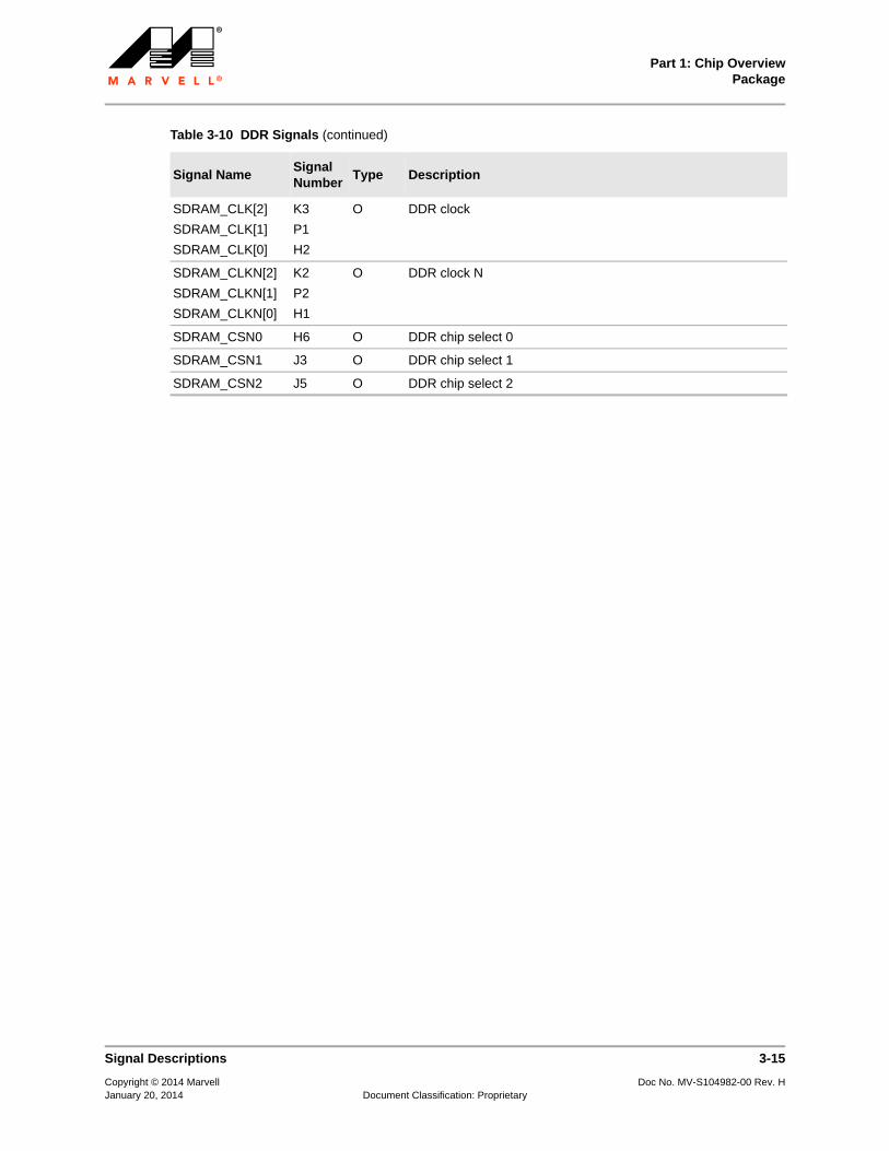
Table 3-10 DDR Signals
Signal NameSignal Number
Type Description
SDRAM_ADDR[15]
SDRAM_ADDR[14]
SDRAM_ADDR[13]
SDRAM_ADDR[12]
SDRAM_ADDR[11]
SDRAM_ADDR[10]
SDRAM_ADDR[9]
SDRAM_ADDR[8]
SDRAM_ADDR[7]
SDRAM_ADDR[6]
SDRAM_ADDR[5]
SDRAM_ADDR[4]
SDRAM_ADDR[3]
SDRAM_ADDR[2]
SDRAM_ADDR[1]
SDRAM_ADDR[0]
T1
T2
R5
R4
R3
R1
P6
P5
N5
N4
M1
N3
M2
M3
M5
M6
O DDR Address
SDRAM_BA[2]
SDRAM_BA[1]
SDRAM_BA[0]
L4
L3
L5
O DDR bank address
SDRAM_CAL_PAD D10 I/O DDR calibration pad.
Tie 300Ω to ground.
SDRAM_CASN J1 O DDR command cycle control signal
SDRAM_CB[7]
SDRAM_CB[6]
SDRAM_CB[5]
SDRAM_CB[4]
SDRAM_CB[3]
SDRAM_CB[2]
SDRAM_CB[1]
SDRAM_CB[0]
V5
V6
T6
U5
V3
U1
U4
T3
I/O 8-bit DDR ECC data
SDRAM_CBM T5 I/O DDR ECC byte mask
SDRAM_CBS V2 I/O DDR ECC byte DQS
SDRAM_CBSB U2 I/O DDR ECC byte DQSB
SDRAM_CKE0 H5 O DDR clock enable 0
SDRAM_CKE1 N1 O DDR clock enable 1
SDRAM_CKE2 P3 O DDR clock enable 2
Part 1: Chip OverviewPackage
Signal Descriptions 3-15
Copyright © 2014 Marvell Doc No. MV-S104982-00 Rev. HJanuary 20, 2014 Document Classification: Proprietary
SDRAM_CLK[2]
SDRAM_CLK[1]
SDRAM_CLK[0]
K3
P1
H2
O DDR clock
SDRAM_CLKN[2]
SDRAM_CLKN[1]
SDRAM_CLKN[0]
K2
P2
H1
O DDR clock N
SDRAM_CSN0 H6 O DDR chip select 0
SDRAM_CSN1 J3 O DDR chip select 1
SDRAM_CSN2 J5 O DDR chip select 2
Table 3-10 DDR Signals (continued)
Signal NameSignal Number
Type Description

88RC9580 R2.3 Eight-Lane PCIe 2.0 to Eight-Port SAS/SATA 6 Gbps RAID-on-Chip Processor Preliminary Datasheet
3-16 Signal Descriptions
Copyright © 2014 Marvell Doc No. MV-S104982-00 Rev. HJanuary 20, 2014 Document Classification: Proprietary
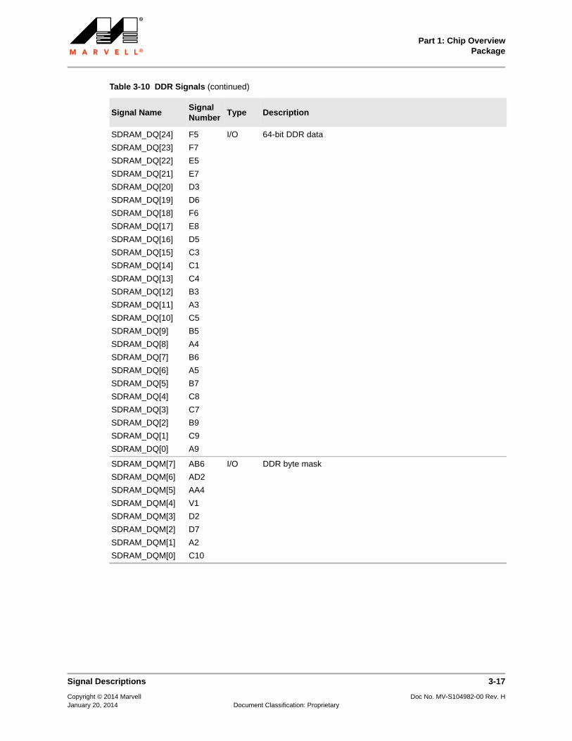
SDRAM_DQ[63]
SDRAM_DQ[62]
SDRAM_DQ[61]
SDRAM_DQ[60]
SDRAM_DQ[59]
SDRAM_DQ[58]
SDRAM_DQ[57]
SDRAM_DQ[56]
SDRAM_DQ[55]
SDRAM_DQ[54]
SDRAM_DQ[53]
SDRAM_DQ[52]
SDRAM_DQ[51]
SDRAM_DQ[50]
SDRAM_DQ[49]
SDRAM_DQ[48]
SDRAM_DQ[47]
SDRAM_DQ[46]
SDRAM_DQ[45]
SDRAM_DQ[44]
SDRAM_DQ[43]
SDRAM_DQ[42]
SDRAM_DQ[41]
SDRAM_DQ[40]
SDRAM_DQ[39]
SDRAM_DQ[38]
SDRAM_DQ[37]
SDRAM_DQ[36]
SDRAM_DQ[35]
SDRAM_DQ[34]
SDRAM_DQ[33]
SDRAM_DQ[32]
SDRAM_DQ[31]
SDRAM_DQ[30]
SDRAM_DQ[29]
SDRAM_DQ[28]
SDRAM_DQ[27]
SDRAM_DQ[26]
SDRAM_DQ[25]
AC8
AE7
AD7
AA8
AC7
AD6
AA7
AB7
AD5
AF5
AE5
AE4
AE3
AE1
AD3
AD1
AC5
AB5
AC3
AC4
AC1
AB3
AA5
AA3
Y6
Y3
AA1
Y5
W4
W5
W3
W1
G1
G3
G5
G4
E1
F3
D1
I/O 64-bit DDR data
Table 3-10 DDR Signals (continued)
Signal NameSignal Number
Type Description
Part 1: Chip OverviewPackage
Signal Descriptions 3-17
Copyright © 2014 Marvell Doc No. MV-S104982-00 Rev. HJanuary 20, 2014 Document Classification: Proprietary
SDRAM_DQ[24]
SDRAM_DQ[23]
SDRAM_DQ[22]
SDRAM_DQ[21]
SDRAM_DQ[20]
SDRAM_DQ[19]
SDRAM_DQ[18]
SDRAM_DQ[17]
SDRAM_DQ[16]
SDRAM_DQ[15]
SDRAM_DQ[14]
SDRAM_DQ[13]
SDRAM_DQ[12]
SDRAM_DQ[11]
SDRAM_DQ[10]
SDRAM_DQ[9]
SDRAM_DQ[8]
SDRAM_DQ[7]
SDRAM_DQ[6]
SDRAM_DQ[5]
SDRAM_DQ[4]
SDRAM_DQ[3]
SDRAM_DQ[2]
SDRAM_DQ[1]
SDRAM_DQ[0]
F5
F7
E5
E7
D3
D6
F6
E8
D5
C3
C1
C4
B3
A3
C5
B5
A4
B6
A5
B7
C8
C7
B9
C9
A9
I/O 64-bit DDR data
SDRAM_DQM[7]
SDRAM_DQM[6]
SDRAM_DQM[5]
SDRAM_DQM[4]
SDRAM_DQM[3]
SDRAM_DQM[2]
SDRAM_DQM[1]
SDRAM_DQM[0]
AB6
AD2
AA4
V1
D2
D7
A2
C10
I/O DDR byte mask
Table 3-10 DDR Signals (continued)
Signal NameSignal Number
Type Description

88RC9580 R2.3 Eight-Lane PCIe 2.0 to Eight-Port SAS/SATA 6 Gbps RAID-on-Chip Processor Preliminary Datasheet
3-18 Signal Descriptions
Copyright © 2014 Marvell Doc No. MV-S104982-00 Rev. HJanuary 20, 2014 Document Classification: Proprietary
SDRAM_DQS[7]
SDRAM_DQS[6]
SDRAM_DQS[5]
SDRAM_DQS[4]
SDRAM_DQS[3]
SDRAM_DQS[2]
SDRAM_DQS[1]
SDRAM_DQS[0]
AF7
AF2
AB2
Y2
F2
E4
B2
A7
I/O DDR byte DQS
SDRAM_DQSB[7]
SDRAM_DQSB[6]
SDRAM_DQSB[5]
SDRAM_DQSB[4]
SDRAM_DQSB[3]
SDRAM_DQSB[2]
SDRAM_DQSB[1]
SDRAM_DQSB[0]
AF6
AF3
AB1
Y1
F1
E3
B1
A8
I/O DDR byte DQSB
SDRAM_ODT0 J4 O On-die termination control 0.
SDRAM_ODT1 H3 O On-die termination control 1.
SDRAM_ODT2 K5 O On-die termination control 2.
SDRAM_RASN K6 O DDR activate cycle control
SDRAM_RESETN E9 O DDR reset N
SDRAM_WEN K1 O DDR write enable.
Table 3-11 System Interface Signals
Signal NameSignal Number
Type Description
PIN_CNFG[1]
PIN_CNFG[0]
AD24
AE26
I Configuration
00: Normal Functional modeOthers:Test Mode
REFCLKP D16 I PCIe reference clock input, 100 MHz HCSL clock.
100MHz ± 300ppm. No internal clock termination.
Table 3-10 DDR Signals (continued)
Signal NameSignal Number
Type Description

Part 1: Chip OverviewPackage
Signal Descriptions 3-19
Copyright © 2014 Marvell Doc No. MV-S104982-00 Rev. HJanuary 20, 2014 Document Classification: Proprietary
REFCLKN C16 I PCIe reference clock input, 100 MHz HCSL clock.
100 MHz ± 300 ppm. No internal clock termination.
PIN_F_TEST[5]
PIN_F_TEST[4]
PIN_F_TEST[3]
PIN_F_TEST[2]
PIN_F_TEST[1]
PIN_F_TEST[0]
AF25
AD23
AD22
W19
AE25
AC22
I Reserved configuration pin.
Note: Pins must be disconnected or pulled high.
Table 3-12 SPI Interface Signals
Signal NameSignal Number
Type Description
PIN_SPI_DI AC26 I SPI data input.
PIN_SPI_CLK AC23 O SPI clock.
PIN_SPI_CS_N Y21 O SPI chip select.
PIN_SPI_DO AC24 O SPI data output.
Table 3-13 PCIe Interface Signals
Signal NameSignal Number
Type Description
HSDACN
HSDACP
G14
H14
I/O, A Analog high-speed DAC pins.
ISET AB21 I/O Chip reference resistor 6 kΩ.
PIN_ISET D22 I Reference Current for PCIe PHY.
This pin must be connected to an external 5 kΩ, 1% resistor to ground.
PIN_M_CLK AA21 I PCIe debugging MDIO interface, clock.
PIN_M_DATA Y20 I/O PCIe debugging MDIO interface, data.
PTP C22 O Analog test port for PCIe
Table 3-11 System Interface Signals (continued)
Signal NameSignal Number
Type Description

88RC9580 R2.3 Eight-Lane PCIe 2.0 to Eight-Port SAS/SATA 6 Gbps RAID-on-Chip Processor Preliminary Datasheet
3-20 Signal Descriptions
Copyright © 2014 Marvell Doc No. MV-S104982-00 Rev. HJanuary 20, 2014 Document Classification: Proprietary
Table 3-14 SAS/SATA Transmitter and Receiver Interface Signals
Signal NameSignal Number
Type Description
PIN_RXN[7]
PIN_RXN[6]
PIN_RXN[5]
PIN_RXN[4]
PIN_RXN[3]
PIN_RXN[2]
PIN_RXN[1]
PIN_RXN[0]
AE21
AE19
AE17
AE15
AD14
AE13
AE11
AF9
I PIN_RXN[7:0]–SAS/SATA PHY 7–0 Receiver Differential Signals.
PIN_RXP[7]
PIN_RXP[6]
PIN_RXP[5]
PIN_RXP[4]
PIN_RXP[3]
PIN_RXP[2]
PIN_RXP[1]
PIN_RXP[0]
AF21
AF19
AF17
AF15
AC14
AF13
AF11
AE9
I PIN_RXP[7:0]–SAS/SATA PHY 7–0 Receiver Differential Signal.
PIN_TXN[7]
PIN_TXN[6]
PIN_TXN[5]
PIN_TXN[4]
PIN_TXN[3]
PIN_TXN[2]
PIN_TXN[1]
PIN_TXN[0]
AD20
AC18
AA17
AC16
AA13
AC12
AA11
AC10
O PIN_TXN[7:0]–SAS/SATA PHY 7–0 Transmitter Differential Signals.
PIN_TXP[7]
PIN_TXP[6]
PIN_TXP[5]
PIN_TXP[4]
PIN_TXP[3]
PIN_TXP[2]
PIN_TXP[1]
PIN_TXP[0]
AC20
AD18
AB17
AD16
AB13
AD12
AB11
AD10
O PIN_TXP[7:0]–SAS/SATA PHY 7–0 Transmitter Differential Signals.

Part 1: Chip OverviewPackage
Signal Descriptions 3-21
Copyright © 2014 Marvell Doc No. MV-S104982-00 Rev. HJanuary 20, 2014 Document Classification: Proprietary
Table 3-15 PCIe Transmitter and Receiver Interface Signals
Signal NameSignal Number
Type Description
PRXN[7]
PRXN[6]
PRXN[5]
PRXN[4]
PRXN[3]
PRXN[2]
PRXN[1]
PRXN[0]
A11
A13
D14
B15
B19
B21
D20
E19
I PRXN[7:0]–PCIe Lane 7–0 Receiver Differential Signals (PCIe RX –).
PRXP[7]
PRXP[6]
PRXP[5]
PRXP[4]
PRXP[3]
PRXP[2]
PRXP[1]
PRXP[0]
B11
B13
C14
A15
A19
A21
C20
F19
I PRXP[7:0]–PCIe Lane 7–0 Receiver Differential Signal (PCIe RX +).
PTXN[7]
PTXN[6]
PTXN[5]
PTXN[4]
PTXN[3]
PTXN[2]
PTXN[1]
PTXN[0]
E11
C12
F13
E15
B17
C18
F17
B23
O PTXN[7:0]–PCIe Lane 7–0 Transmitter Differential Signals (PCIe TX –).
PTXP[7]
PTXP[6]
PTXP[5]
PTXP[4]
PTXP[3]
PTXP[2]
PTXP[1]
PTXP[0]
F11
D12
E13
F15
A17
D18
E17
A23
O PTXP[7:0]–PCIe Lane 7–0 Transmitter Differential Signals (PCIe TX +).

88RC9580 R2.3 Eight-Lane PCIe 2.0 to Eight-Port SAS/SATA 6 Gbps RAID-on-Chip Processor Preliminary Datasheet
3-22 Signal Descriptions
Copyright © 2014 Marvell Doc No. MV-S104982-00 Rev. HJanuary 20, 2014 Document Classification: Proprietary
Table 3-16 Power Interface Signals
Signal NameSignal Number
Type Description
AVDD[4-7_8] G11, G12, G13, H10, H11, H12, H13
Power, I 1.8V analog power for PCIe PHY and PCIe.
AVDD[0-3_8] G16, G17, G18, H15, H16, H17, H18
AVDD25_0
AVDD25_1
G10
D23
Power, I I/O Pad Power 2.5V.
AVDD_DDR L1 Power, I DDR DLL power.
AVDD_DDR is at the same level as VDDQ (1.8V, 1.5V).
VAA[4-7] AA15, AA19, AB15, AB19, Y15, Y16, Y17, Y18
Power, I 2.5V analog power for SAS/Serial ATA PHY.
VAA[0-3] AA9, AB9, Y9, Y10, Y11, Y12, Y13, Y14
Power, I 2.5V analog power for SAS/Serial ATA PHY.
VAA_ANA Y19 Power, I 2.5V analog power for chip PLL and current source.
VAA_PLL AA20 Power, I 2.5V power for CPU and DDR PLL.
VDD K9, K11, K13, K15, K17, L10, L12, L14, L16, M11, M13, M15, M17, N10, N12, N14, N16, P9, P11, P13, P15, P17, R10, R12, R14, R16, T9, T11, T13, T15, T17, U10, U12, U14, U16, V9, V11, V13, V15, V17
Power, I 1.0V digital core power.

Part 1: Chip OverviewPackage
Signal Descriptions 3-23
Copyright © 2014 Marvell Doc No. MV-S104982-00 Rev. HJanuary 20, 2014 Document Classification: Proprietary
VDDO1 J18, K18, L18, M18, N18, P18, P19, R18, T18, U18, V18, W18
Power, I Digital Power.
3.3V I/O Power to supply digital and I/Os.
VDDQ AB4, AB8, AD4, AD8, AF4, B4, B8, D4, D8, F4, F8, G7, H4, H7, J7, K4, K7, L7, M4, M7, N7, P4, P7, R7, T4, T7, U7, V4, V7,
W7, Y4, Y7
Power, I DDR2/DDR3 I/O Power 1.8V/1.5V.
VHV AB22 Power Power supply for One-Time-Program (OTP). Typical is 2.5V for
Program mode and 1.0V or 2.5V for read mode.
VREFD F9 Power, I DDR PHY reference voltage, half VDDQ.
VREFS D9 Power, I DDR PHY reference voltage, half VDDQ.
Table 3-16 Power Interface Signals (continued)
Signal NameSignal Number
Type Description

88RC9580 R2.3 Eight-Lane PCIe 2.0 to Eight-Port SAS/SATA 6 Gbps RAID-on-Chip Processor Preliminary Datasheet
3-24 Signal Descriptions
Copyright © 2014 Marvell Doc No. MV-S104982-00 Rev. HJanuary 20, 2014 Document Classification: Proprietary
VSS A1, A6, A10, A12, A14, A16, A18, A20, A22, A24, A26, B10, B12, B14, B16, B18, B20, B22, B24, C2, C6, C11, C13, C15, C17, C19, C21, C23, D11, D13, D15, D17, D19, D21, E2, E6, E10, E12, E14, E16, E18, E20, F10, F12, F14, F16, F18, F20, G2, G6, G8, G9, G15, G19, H8, H9, J2, J6, J8, J9, J10, J11, J12, J13, J14, J15, J16, J17, K8, K10, K12, K14, K16, L2, L6, L8, L9, L11, L13, L15, L17, M8, M10, M12, M14, M16, N2, N6, N8, N9, N11, N13, N15, N17, P8, P10, P12, P14, P16
Ground Ground.
Table 3-16 Power Interface Signals (continued)
Signal NameSignal Number
Type Description

Part 1: Chip OverviewPackage
Signal Descriptions 3-25
Copyright © 2014 Marvell Doc No. MV-S104982-00 Rev. HJanuary 20, 2014 Document Classification: Proprietary
VSS R2, R6, R8, R9, R11, R13, R15, R17, T8, T10, T12, T14, T16, U3, U6, U8, U9, U11, U13, U15, U17, V8, V10, V12, V14, V16, W2, W6, W8, W9, W10, W11, W12, W13, W14, W15, W16, W17, Y8, AA2, AA6, AA10, AA12, AA14, AA16, AA18, AB10, AB12, AB14, AB16, AB18, AB20, AC2, AC6, AC9, AC11, AC13, AC15, AC17, AC19, AC21, AD9, AD11, AD13, AD15, AD17, AD19, AD21
Ground Ground.
Table 3-16 Power Interface Signals (continued)
Signal NameSignal Number
Type Description

88RC9580 R2.3 Eight-Lane PCIe 2.0 to Eight-Port SAS/SATA 6 Gbps RAID-on-Chip Processor Preliminary Datasheet
3-26 Signal Descriptions
Copyright © 2014 Marvell Doc No. MV-S104982-00 Rev. HJanuary 20, 2014 Document Classification: Proprietary
VSS AE2, AE6, AE8, AE10, AE12, AE14, AE16, AE18, AE20, AE22, AF1, AF8, AF10, AF12, AF14, AF16, AF18, AF20, AF22, AF26
Ground Ground.
Table 3-16 Power Interface Signals (continued)
Signal NameSignal Number
Type Description

Part 1: Chip OverviewLayout Guidelines
4-1
Copyright © 2014 Marvell Doc No. MV-S104982-00 Rev. HJanuary 20, 2014 Document Classification: Proprietary
4 LAYOUT GUIDELINES
This chapter describes the system recommendations from the Marvell Semiconductor design and application engineers who work with the 88RC9580. It is written for those who are designing schematics and printed circuit boards for an 88RC9580-based system. Whenever possible, the PCB designer should try to follow the suggestions provided in this chapter.
The information in this chapter is preliminary. Please consult with Marvell Semiconductor design and application engineers before starting your PCB design.
This chapter contains the following sections:
88RC9580 Board Schematics
. Layer Stack-Up
Power Supply
PCB Trace Routing
Recommended Layout
Refer to Chapter 3, Package, for package information.

88RC9580 R2.3 Eight-Lane PCIe 2.0 to Eight-Port SAS/SATA 6 Gbps RAID-on-Chip Processor Preliminary Datasheet
4-2 88RC9580 Board Schematics
Copyright © 2014 Marvell Doc No. MV-S104982-00 Rev. HJanuary 20, 2014 Document Classification: Proprietary
4.1 88RC9580 Board Schematics
This section contains board schematics for the 88RC9580.
The following figures are included in this section:
Figure 4-1, 88RC9580 Overview
Figure 4-2, 88RC9580 Power and Reset
Figure 4-3, 88RC9580 System
Figure 4-4, 88RC9580 LED and GPIO
Figure 4-5, 88RC9580 PCIe x8
Figure 4-6, 88RC9580 PBSRAM, NVRAM, and NOR
Figure 4-7, 88RC9580 DDR2, and DDR3
Figure 4-8, 88RC9580 SAS and SATA
Figure 4-9, 88RC9580 Power VAA and VDD
Figure 4-10, 88RC9580 Power Ground
Figure 4-11, 88RC9580 DDR3 CHIPS
Figure 4-12, 88RC9580 System BKUP Power
Figure 4-13, 88RC9580 DDR3 VDD/VTT Power
Figure 4-14, 88RC9580 Bootstrap
Figure 4-1 88RC9580 Overview
888RC9580
PCIE X8 GOLD FINGER
PCIE X 8
SAS/SATA PORTS 0~3 SAS/SATA PORTS 4~7
DDR3x16 8GBitDDR3 BUS
P_DATA/ADDRNVRAM 128KB
NOR FLASH 64MBitBOOT FLASH 2MBIT
THERMAL SENSOR
SPD EEPROM 2KBit
SPI
I2C_2
HEADER
BATTERY I2C_1
EEPROM 4KBitI2C_0
JTAG & UART0JTAG and UART0 HEADER
50MHz Reference Clock
UART1 JACKUART1

Part 1: Chip OverviewLayout Guidelines
88RC9580 Board Schematics 4-3
Copyright © 2014 Marvell Doc No. MV-S104982-00 Rev. HJanuary 20, 2014 Document Classification: Proprietary
Figure 4-2 88RC9580 Power and Reset
PCIE RESET#
AND GATE
PIN_PRESET_N
PIN_RESET_N
PFAIL
nSRST
RESET BUTTON
AS_nTRST
nSRST
RESET PATH
5V/300mA
1.5V_DDR3/1.3A5V/0.5A
5V/500mA
0.75V/500mA3.3VDUAL/50mA
5V/0.7A5V/0.7A
3.7V/1880mAh
LDO
Core
DDR Controller
SAS/SATA
I/O
Digital+Analog
Reference&Termination
Vout1
Vout2
MVPG31
PCIE CONN
12V/1.4A
5V/1.95A12V/1A
12V/0.4A
+
POWERMUX
88PG847
88PG847
1V/3.5A
1.5V/800mA
2.5V/850mA
3.3V/200mA
LTC3850
DDR3
TPS51200
MVPG31+
+
1.8V/800mA5V/450mA
POWER PATH
JTAG debugport
1.5V_DDR3/300mA
+
+
1.5V_DDR3/1A
PCIE3V3/3.0A
PCIE12V/2.1A

88RC9580 R2.3 Eight-Lane PCIe 2.0 to Eight-Port SAS/SATA 6 Gbps RAID-on-Chip Processor Preliminary Datasheet
4-4 88RC9580 Board Schematics
Copyright © 2014 Marvell Doc No. MV-S104982-00 Rev. HJanuary 20, 2014 Document Classification: Proprietary
Figure 4-3 88RC9580 System
I2C ADDR:1010 000
EEPROM
TEMP. SENSOR
I2C ADDR:1001 000
I2C ADDR:1010 000
EEPROM
I2C0
I2C2
JTAG & UART-0
SPI FLASH
PD=10mA
PD=5mA
PD=5mA
UART1 ( DCE SIDE )
When PCIE12V disappeared
PFAIL = 0 : BBU_REQ enable
RTC
BUZZER
LOW ACTIVE
50MHz OSC
Kyocera KC3225A50.0000C2GE00 (Temp. -40 to +85)
Kyocera KC3225A50.0000C20E00 (Temp. -10 to +70)
Epson SG-310SDN 50.0000MJ3 (Temp. -40 to +85)
REV 5: Remove U8(74LVC1G08), PIN_RESET_N can not gate with PFAIL#
REV 5: change 3.3VDUAL to 2V5
REV 5: Change OSC1 to 2V5 device
REV 5
REV 5
OS
C_5
0MH
z
PIN
_RE
SE
T_N
AS
_TD
OA
S_T
DI
AS
_TC
K
AS
_TM
S
nSR
ST
UA
O_0
AS
_TD
IA
S_n
TRS
T
UA
I_0
AS
_TD
O
AS
_TC
KA
S_T
MS
PIN
_PR
ES
ET_
N
PIN
_RE
SE
T_N
CN
FG0
CN
FG1
UA
O_0
UA
I_0
UA
I_1
UA
O_1
nSR
ST
AS
_nTR
ST
SP
I_D
IS
PI_
DO
SP
I_C
LKS
PI_
CS
_N
SP
I_D
O
SP
I_C
LK
SP
I_C
S_N
SC
L_1
SC
L_2
SD
A_1
SC
L_0
SD
A_0
SD
A_2
TES
T14
TES
T15
TES
T5TE
ST6
TES
T7TE
ST8
TES
T9TE
ST1
0TE
ST1
1TE
ST1
2TE
ST1
3
TES
T0TE
ST1
TES
T2TE
ST3
TES
T4
SP
I_D
I_J
SC
L_2
SD
A_2
SC
L_0
SD
A_0
SP
I_D
I
TEM
P_A
LER
T
MD
IO_C
LKM
DIO
_DA
T
AD
M1_
TXA
DM
1_R
XA
DM
0_R
XU
AO
_1
PFA
IL#
PIN
_TP
AD
M0_
TXU
AI_
1
RTC
_X2
RTC
_X1
TES
T8
TES
T9
BB
U_R
EQ
RTC
_BA
T
2V5
3V3
3V3
3V3
3V3
3V3
3V3
3V3
3V3
3V3
3V3
3V3
3V3
5V0
3V3
3V3
3V3
2V5
SD
A_1
12S
CL_
112
PIN
_PR
ES
ET_
N5
PO
R12
,13
PFA
IL#
5,13
CN
FG[1
..0]
14
TES
T[15
..0]
14
GP
IO0
4
SD
A_0
8S
CL_
08
SD
A_2
8S
CL_
28
U3
AT2
4C04
BNA0
1
A12
A23
GN
D4
SDA
5SC
L6
WP
7
VCC
8
R10
70-
5%R
0402
R7 4.7K-5%R0402
EMIFIL
(P2 GND)
FIL1
022
00pF
L080
5-3
C12
100n
FC
0402
10V
Q6
2N70
02
3
1
2
C1
100n
FC
0402
10V
R6 4.7K-5%R0402
BA
T2
DN
P_3
.1V
_BA
T
1 2
U6
TMP
75A
IDG
KT
A07
A16
A25
VCC
8
GN
D4
ALER
T3
SCL
2
SDA
1
DB
1
SH
_2x5
_2.5
4
11
22
33
44
55
66
77
88
99
1010
+
LED
1YE
LLO
W
U5
MX
25L4
006E
CS#
1
SO2
WP#
3SI
5
SCLK
6
HO
LD#
7VC
C8
Gnd
4
C10
100n
FC
0402
10V
I2C
2
22-0
5-50
35
11
22
33
R3 4.7K-5%R0402
R19
1K-5
%R
0603
UA
RT1
SJ-
3523
AU
DIO
-JA
CK
-SJ-
3523
-SM
T
GN
D1
RXO
2TX
I3
J44
J55
BU
ZZ1
BU
ZZE
R_3
VD
C
1 2
R12
90-
5%R
0402
C4
100n
FC
0402
10V
TP2TP
1
88R
C95
80
U2A PI
N_B
BU_R
EQE2
1
PIN
_M_C
LKAA
21
PIN
_M_D
ATA
Y20
PIN
_NSR
STAE
23
PIN
_NTR
STAE
24
PIN
_PR
ESET
_NAD
25
PIN
_REF
CLK
AF24
PIN
_RES
ET_N
V19
PIN
_SC
L[0]
L19
PIN
_SC
L[1]
J26
PIN
_SC
L[2]
J24
PIN
_SD
A[0]
K26
PIN
_SD
A[1]
J25
PIN
_SD
A[2]
K21
PIN
_TP
AF23
PIN
_UAI
[0]
K23
PIN
_UAI
[1]
K22
PIN
_UAO
[0]
L20
PIN
_UAO
[1]
L21
PIN
_SPI
_CLK
AC23
PIN
_SPI
_CS_
NY2
1
PIN
_SPI
_DI
AC26
PIN
_SPI
_DO
AC24
PIN
_TC
KL2
2
PIN
_TD
IK2
4
PIN
_TD
OM
19
PIN
_TM
SK2
5
PIN
_CN
FG[0
]AE
26
PIN
_CN
FG[1
]AD
24
PIN
_TES
T[0]
F25
PIN
_TES
T[1]
G21
PIN
_TES
T[10
]E2
2
PIN
_TES
T[11
]D
26
PIN
_TES
T[12
]C
26
PIN
_TES
T[13
]A2
5
PIN
_TES
T[14
]C
25
PIN
_TES
T[15
]E2
3
PIN
_TES
T[2]
H20
PIN
_TES
T[3]
F23
PIN
_TES
T[4]
F22
PIN
_TES
T[5]
J19
PIN
_TES
T[6]
F24
PIN
_TES
T[7]
E26
PIN
_TES
T[8]
E25
PIN
_TES
T[9]
E24
C5
100n
FC
0402
10V
OS
C1
50M
Hz
KC
3225
A50
.000
0C2G
E00
VCC
4
GN
D2
CKQ
3
OE/
NC
1
JP1
DN
P_U
H_2
x1_2
.54
1
2
R11
20-
5%R
0402
C30
12pF
C04
0250
V
R14 10K-5%R0402
CN
1
DN
P_C
ON
_3x1
_2.5
4
U7
AD
M32
02A
RN
C1+
1
V+2
C1-
3
V-6
C2+
4
C2-
5
3.3V
16
GN
D15
Tx1I
N11
Tx2I
N10
Rx1
OU
T12
Rx2
OU
T9
Tx1O
UT
14
Tx2O
UT
7R
x1IN
13
Rx2
IN8
C6
100n
FC
0402
10V
R17
1K-5
%R
0402
R5 4.7K-5%R0402
R11 10K-5%R0402
R12
30-
5%R
0402
R12
21K
-5%
R04
02
R21
DN
P_1
M-1
%R
0603
C7
12pF
C04
0250
V
SW
1P
SID
E-4
PIN
1234
C8
100n
FC
0402
10V
R10 10K-5%R0402
HS
1
MFA
5040
-12P
/3.8
Y+T7
25
Q7
2N70
02
3
1
2
Y1 32.7
68K
Hz
U4
AT2
4C02
BNA0
1
A12
A23
GN
D4
SDA
5SC
L6
WP
7
VCC
8
C11
100n
FC
0402
10V
R18
0-5%
R04
02
R4 4.7K-5%R0402
UA
RTH
1
UH
_3x1
_2.5
4
1 2 3
I2C
0
22-0
5-50
35
11
22
33
Q1
2N70
02
3
1
2
XJP
1D
NP
_SH
UN
T
C3
10nF
C04
0216
VR
1510
K-5
%R
0402
C9
100n
FC
0402
10V
R9 10K-5%R0402
C2
100n
FC
0402
10V
U9
DS
1388
Z-33
+X11
X22
VBAT
3
GN
D4
SDA
5SC
L6
RST
7VC
C8
R8 DNP_4.7K-5%R0402
R12 10K-5%R0402

Part 1: Chip OverviewLayout Guidelines
88RC9580 Board Schematics 4-5
Copyright © 2014 Marvell Doc No. MV-S104982-00 Rev. HJanuary 20, 2014 Document Classification: Proprietary
Figure 4-4 88RC9580 LED and GPIO
Co-use for SAS Sideband
PIN_F_TEST[5:0] must unconnected or pull high
Top - Activity (Green)
Bottom - Fault (Yellow)
FLT3
FLT0
FLT1
FLT2
FLT4
FLT5
FLT6
FLT7
FLT8
FLT3
S_C
LK0
FLT0
S_D
IN0
FLT1
S_D
OU
T0FL
T2S
_LO
AD
0
FLT4
S_D
IN1
FLT5
S_D
OU
T1FL
T6S
_LO
AD
1FL
T7S
_CLK
1
PIN
_F_T
ES
T0P
IN_F
_TE
ST1
PIN
_F_T
ES
T2P
IN_F
_TE
ST3
PIN
_F_T
ES
T4P
IN_F
_TE
ST5
AC
T0A
CT1
AC
T2A
CT3
AC
T4A
CT5
AC
T6A
CT7
AC
T8
FLT8
AC
T8
FLT0
FLT1
FLT2
FLT3
FLT4
FLT5
FLT6
FLT7
GP
IO1
GP
IO6
GP
IO7
GP
IO0
GP
IO1
GP
IO6
3V3
3V3
3V3
3V3
3V3
3V3
S_D
IN0
8S
_DO
UT0
8
S_C
LK0
8S
_LO
AD
08
S_D
OU
T18
S_D
IN1
8
S_C
LK1
8S
_LO
AD
18
Cha
rger
_EN
#12
Latc
h_E
N12P
WR
_Sw
itch_
CTL
12
Pow
er_s
witc
h_Q
112
GP
IO0
3
GP
IO1
8
GP
IO6
8
R68
1K-5
%R
0402
R11
71K
-5%
R04
02
R79
DN
P_1
0K-5
%R
0402
+FLT
3R
ED
R63
1K-5
%R
0402
+
AC
T2G
RE
EN
R21
72K
-5%
R04
02
R70
1K-5
%R
0402
+FLT
5R
ED
+A
CT4
GR
EE
N
R80
DN
P_1
0K-5
%R
0402
R67
1K-5
%R
0402
+FLT
7R
ED
R21
82K
-5%
R04
02
+
AC
T6G
RE
EN
+
LED
7YE
LLO
W
R72
1K-5
%R
0402
+FLT
1R
ED
+
AC
T8G
RE
EN
R69
1K-5
%R
0402
+
LED
8YE
LLO
WR
81D
NP
_10K
-5%
R04
02
R71
1K-5
%R
0402
R22
02K
-5%
R04
02
R58
1K-5
%R
0402
R73
1K-5
%R
0402
R22
12K
-5%
R04
02
R10
81K
-5%
R04
02
+FLT
2R
ED
R76
DN
P_1
0K-5
%R
0402
R22
22K
-5%
R04
02
R12
11K
-5%
R04
02
+FLT
4R
ED
+
AC
T3G
RE
EN
R62
1K-5
%R
0402
88R
C95
80
U2B PIN
_AC
T[0]
H26
PIN
_AC
T[1]
J21
PIN
_AC
T[2]
J23
PIN
_AC
T[3]
K20
PIN
_AC
T[4]
H25
PIN
_AC
T[5]
J22
PIN
_AC
T[6]
K19
PIN
_AC
T[7]
H23
PIN
_AC
T[8]
J20
PIN
_GP
IO[0
]C
24
PIN
_GP
IO[1
]B
26
PIN
_GP
IO[2
]D
24
PIN
_GP
IO[3
]F2
1
PIN
_GP
IO[4
]G
20
PIN
_GP
IO[5
]B
25
PIN
_GP
IO[6
]D
25
PIN
_GP
IO[7
]H
19
PIN
_F_T
ES
T[0]
AC
22
PIN
_F_T
ES
T[1]
AE
25
PIN
_F_T
ES
T[2]
W19
PIN
_F_T
ES
T[3]
AD
22
PIN
_F_T
ES
T[4]
AD
23
PIN
_F_T
ES
T[5]
AF2
5
PIN
_FLT
[0]
G24
PIN
_FLT
[1]
H21
PIN
_FLT
[2]
H22
PIN
_FLT
[3]
G25
PIN
_FLT
[4]
G26
PIN
_FLT
[5]
H24
PIN
_FLT
[6]
G23
PIN
_FLT
[7]
G22
PIN
_FLT
[8]
F26
+FLT
6R
ED
+
AC
T5G
RE
EN
R59
1K-5
%R
0402
R22
32K
-5%
R04
02
GREE
N
YELL
OW
GLE
D1
GR
N/Y
EL
21
43
+FLT
8R
ED
+
AC
T7G
RE
EN
R60
1K-5
%R
0402
R11
11K
-5%
R04
02
R22
42K
-5%
R04
02
R11
91K
-5%
R04
02
R66
1K-5
%R
0402
R10
91K
-5%
R04
02
R61
1K-5
%R
0402
R64
1K-5
%R
0402
R77
DN
P_1
0K-5
%R
0402
+
LED
5YE
LLO
W
R78
DN
P_1
0K-5
%R
0402
+
AC
T1G
RE
EN
R65
1K-5
%R
0402
+
LED
6YE
LLO
W
R21
62K
-5%
R04
02

88RC9580 R2.3 Eight-Lane PCIe 2.0 to Eight-Port SAS/SATA 6 Gbps RAID-on-Chip Processor Preliminary Datasheet
4-6 88RC9580 Board Schematics
Copyright © 2014 Marvell Doc No. MV-S104982-00 Rev. HJanuary 20, 2014 Document Classification: Proprietary
Figure 4-5 88RC9580 PCIe x8
PCIE POWER DETECTOR
REV 5
HSI
N7
PRXN
5PR
XP5
HSO
N5
HSO
P5
PRXN
4PR
XP4
HSO
N4
HSO
P4
PTXN
7
PRXN
3PR
XP3
HSI
P7PT
XP7
HSI
N6
PTXN
6H
SIP6
PTXP
6
HSO
P0PR
XN0
HSO
N0
PRXP
0
HSI
N5
PTXN
5H
SIP5
PTXP
5
HSO
P1
HSI
N4
PTXN
4H
SIP4
PTXP
4
HSI
N3
PTXN
3H
SIP3
PTXP
3
PRXN
7
HSO
N1
PCLK
N
HSI
N2
PTXN
2H
SIP2
PTXP
2
PCLK
P
HSI
N1
PTXN
1H
SIP1
PTXP
1
HSO
P2
PRXN
1PR
XP1
HSI
N0
PTXN
0H
SIP0
PTXP
0
HSO
N2
PRXP
7
HSO
P3
PRXN
2PR
XP2
HSO
N7
HSO
P7
HSO
N3
PRXN
6PR
XP6
HSO
N6
PCIE
_3V3
HSO
P6PT
XN6
PTXP
6
PTXN
5PT
XP5
PTXN
4PT
XP4
PTXN
7PT
XP7
PTXN
3PT
XP3
PTXN
2PT
XP2
PTXN
1PT
XP1
PTXN
0PT
XP0
HSD
ACN
HSD
ACP
PTP
PRXN
6PR
XP6
PRXN
5PR
XP5
PRXN
4PR
XP4
PRXN
3PR
XP3
PRXN
2PR
XP2
PRXN
1PR
XP1
PRXN
0PR
XP0
PRXN
7PR
XP7
PCLK
N
PCLK
P
PFAI
L#
PIN
_ISE
T
3V3
PCIE
_3V3
PCIE
_12V
PCIE
_12V
PCIE
_3V3
3V3
3V3
PIN
_PR
ESET
_N3
PFAI
L#3,
13
R2
1K-1
%R
0402
C15
100n
FC
0402
R10
00-
5%R
0402
R13
34.
99K-
1%R
0402
R99
DN
P_0-
5%R
0402
R97
0-5%
R04
02
R1
6.04
K-1%
R04
02
C20
100n
FC
0402
R85
0-5%
R04
02
R96
0-5%
R04
02
R94
0-5%
R04
02
R91
0-5%
R04
02
R83
0-5%
R04
02
R87
0-5%
R04
02
R89
0-5%
R04
02
C18
100n
FC
0402
TP3
TP5
PCIE x8
TOP
BOTP1 DN
P_PC
IEx8
_Gol
d Fi
nger
+12V
_3B
1+1
2V_4
B2
RSV
D_4
B3
GN
D_1
9B
4SM
CLK
B5
SM
DA
TB
6G
ND
_20
B7
3V3_
3B
8TR
ST#
B9
3.3V
Aux
B10
WA
KE
#B
11
RSV
D_5
B12
GN
D_2
1B
13H
SOp(
0)B
14H
SOn(
0)B
15G
ND
_22
B16
PRSN
T#2A
B17
GN
D_2
3B
18H
SOp(
1)B
19H
SOn(
1)B
20G
ND
_24
B21
GN
D_2
5B
22H
SOp(
2)B
23H
SOn(
2)B
24G
ND
_26
B25
GN
D_2
7B
26H
SOp(
3)B
27H
SOn(
3)B
28G
ND
_28
B29
RSV
D_6
B30
PRSN
T#2B
B31
GN
D_2
9B
32
PRSN
T#1
A1
+12V
_1A
2+1
2V_2
A3
GN
D_1
A4
TCK
A5
TDI
A6
TDO
A7
TMS
A8
3V3_
1A
93V
3_2
A10
PWR
GD
A11
GN
D_2
A12
REF
CLK
+A
13R
EFC
LK-
A14
GN
D_3
A15
HSI
p(0)
A16
HSI
n(0)
A17
GN
D_4
A18
RSV
D_1
A19
GN
D_5
A20
HSI
p(1)
A21
HSI
n(1)
A22
GN
D_6
A23
GN
D_7
A24
HSI
p(2)
A25
HSI
n(2)
A26
GN
D_8
A27
GN
D_9
A28
HSI
p(3)
A29
HSI
n(3)
A30
GN
D_1
0A
31R
SVD
_2A
32R
SVD
_3A
33H
SIp(
4)A
35H
SIn(
4)A
36G
ND
_12
A37
GN
D_1
3A
38H
SIp(
5)A
39H
SIn(
5)A
40G
ND
_14
A41
GN
D_1
5A
42
GN
D_1
1A
34
HSI
p(6)
A43
HSI
n(6)
A44
GN
D_1
6A
45G
ND
_17
A46
HSI
p(7)
A47
HSI
n(7)
A48
GN
D_1
8A
49
HSO
p(4)
B33
HSO
n(4)
B34
GN
D_3
0B
35G
ND
_31
B36
HSO
p(5)
B37
HSO
n(5)
B38
GN
D_3
2B
39G
ND
_33
B40
HSO
p(6)
B41
HSO
n(6)
B42
GN
D_3
4B
43G
ND
_35
B44
HSO
p(7)
B45
HSO
n(7)
B46
GN
D_3
6B
47PR
SNT#
2CB
48G
ND
_37
B49
C21
100n
FC
0402
C23
100n
FC
0402
C25
100n
FC
0402
C27
100n
FC
0402
C29
100n
FC
0402
C14
100n
FC
0402
R10
20-
5%R
0402
R98
0-5%
R04
02TP
4
R20
10K-
5%R
0402
U1
TPS3
805
NC
1
GN
D2
RE
SE
T3
VDD
4
SE
NS
E5
C16
100n
FC
0402
R95
0-5%
R04
02
R93
0-5%
R04
02
R90
0-5%
R04
02
R86
0-5%
R04
02
R88
0-5%
R04
02
R92
DN
P_0-
5%R
0402
C17
100n
FC
0402
PCIE
88R
C95
80
U2C PR
XN[0
]E
19
PRXN
[1]
D20
PRXN
[2]
B21
PRXN
[3]
B19
PRXN
[4]
B15
PRXN
[5]
D14
PRXN
[6]
A13
PRXN
[7]
A11
PR
XP[0
]F1
9
PR
XP[1
]C
20
PR
XP[2
]A
21
PR
XP[3
]A
19
PR
XP[4
]A
15
PR
XP[5
]C
14
PR
XP[6
]B
13
PR
XP[7
]B
11
PTX
N[0
]B
23
PTX
N[1
]F1
7
PTX
N[2
]C
18
PTX
N[3
]B
17
PTX
N[4
]E
15
PTX
N[5
]F1
3
PTX
N[6
]C
12
PTX
N[7
]E
11
PTX
P[0
]A
23
PTX
P[1
]E
17
PTX
P[2
]D
18
PTX
P[3
]A
17
PTX
P[4
]F1
5
PTX
P[5
]E
13
PTX
P[6
]D
12
PTX
P[7
]F1
1
HSD
ACN
G14
HSD
ACP
H14
PTP
C22
PIN
_ISE
TD
22
REF
CLK
NC
16
REF
CLK
PD
16
R10
30-
5%R
1206
C19
100n
FC
0402
C22
100n
FC
0402
C24
100n
FC
0402
R13
1K-1
%R
0402
C26
100n
FC
0402
C28
100n
FC
0402
R84
0-5%
R04
02
R16
DN
P_10
0-1%
R04
02

Part 1: Chip OverviewLayout Guidelines
88RC9580 Board Schematics 4-7
Copyright © 2014 Marvell Doc No. MV-S104982-00 Rev. HJanuary 20, 2014 Document Classification: Proprietary
Figure 4-6 88RC9580 PBSRAM, NVRAM, and NOR
NVRAM 128KB
NOR FLASH 64Mb
P_D
ATA0
P_D
ATA1
P_D
ATA2
P_D
ATA3
P_D
ATA4
P_D
ATA5
P_D
ATA6
P_D
ATA7
P_D
ATA8
P_D
ATA9
P_D
ATA1
0P_
DAT
A11
P_D
ATA1
2P_
DAT
A13
P_D
ATA1
4P_
DAT
A15
P_AD
DR
0
N_W
E_N
N_C
E_N
N_O
E_N
F_R
ESET
_NF_
CE_
NF_
REA
DY
F_W
E_N
F_O
E_N
F_BY
TE_N
P_AD
DR
1P_
ADD
R2
P_AD
DR
3P_
ADD
R4
P_AD
DR
5P_
ADD
R6
P_AD
DR
7P_
ADD
R8
P_AD
DR
9P_
ADD
R10
P_AD
DR
11P_
ADD
R12
P_AD
DR
13P_
ADD
R14
P_AD
DR
15P_
ADD
R16
P_AD
DR
17P_
ADD
R18
P_AD
DR
19P_
ADD
R20
P_AD
DR
21P_
ADD
R22
P_AD
DR
23
P_D
ATA0
P_D
ATA1
P_D
ATA2
P_D
ATA3
P_D
ATA4
P_D
ATA5
P_D
ATA6
P_D
ATA7
P_AD
DR
0
P_AD
DR
3P_
ADD
R2
P_AD
DR
1
P_AD
DR
5P_
ADD
R4
P_AD
DR
6P_
ADD
R7
P_AD
DR
9P_
ADD
R8
P_AD
DR
10P_
ADD
R11
P_AD
DR
12P_
ADD
R13
P_AD
DR
14P_
ADD
R15
P_AD
DR
16
F_R
EAD
Y
F_W
E_N
F_C
E_N
F_O
E_N
P_AD
DR
20P_
ADD
R21
P_AD
DR
0P_
ADD
R1
P_AD
DR
2P_
ADD
R3
P_AD
DR
4P_
ADD
R5
P_AD
DR
6P_
ADD
R7
P_AD
DR
8P_
ADD
R9
P_AD
DR
10P_
ADD
R11
P_AD
DR
12P_
ADD
R13
P_AD
DR
14P_
ADD
R15
P_AD
DR
16P_
ADD
R17
P_AD
DR
18P_
ADD
R19
P_D
ATA0
P_D
ATA1
P_D
ATA2
P_D
ATA3
P_D
ATA4
P_D
ATA5
P_D
ATA6
P_D
ATA7
P_D
ATA8
P_D
ATA9
P_D
ATA1
0P_
DAT
A11
P_D
ATA1
2P_
DAT
A13
P_D
ATA1
4P_
DAT
A15
N_W
E_N
N_C
E_N
N_O
E_N
F_R
ESET
_N
F_BY
TE_N
3V3
3V3
3V3 C
5010
0nF
C04
0210
V
C47
100n
FC
0402
10V
U13
CY1
4B10
1LA-
SP25
XI
Vca
p1
A16
2A
143
A12
4
A7
5A
66
A5
7
NC
18
A4
9
NC
210
NC
311
NC
412
VS
S1
13
NC
514
NC
615
DQ
016
A3
17A
218
A1
19A
020
NC
723
NC
824
VS
S2
36
NC
1137
NC
1238
NC
1339
A11
40
NC
1441
A9
42A
843
A13
44
NC
1035
NC
934
DQ
633
OE
#32
A10
31
CE#
30
VCC
248
A15
47
HS
B#
46W
E#
45
DQ
729
DQ
528
DQ
427
DQ
326
VC
C1
25
DQ
121
DQ
222
+
C49
100u
FTC
3216
6V3
TP7
R11
60-
5%R
0402
C48
100n
FC
0402
10V
U14
MX2
9LV6
40ET
NO
R F
LASH
A0
E1
A1
D1
A2
C1
A3
A1
A4
B1
A5
D2
A6
C2
A7
A2
A8
B5
A9
A5
A10
C5
A11
D5
A12
B6
A13
A6
A14
C6
A15
D6
A16
E6
A17
B2
A18
C3
A19
D4
A20
D3
A21
C4
RY/
BYA
3
WP
/AC
CB
3
WE
A4
CE
F1
OE
G1
RES
ETB
4
DQ
0E
2
DQ
1H
2
DQ
2E
3
DQ
3H
3
DQ
4H
4
DQ
5E
4
DQ
6H
5
DQ
7E
5
DQ
8F2
DQ
9G
2
DQ
10F3
DQ
11G
3
DQ
12F4
DQ
13G
5
DQ
14F5
DQ
15/A
-1G
6
VC
CG
4
BYT
E/N
CF6
VS
S1
H1
VS
S2
H6
11
22
R11
310
K-5%
R04
02
R11
410
K-5%
R04
02
R11
8D
NP_
10K-
5%R
0402
pbSRAM
NVSRAM
FLASH
88R
C95
80
U2D P
IN_F
_BYT
E_N
M23
PIN
_F_C
E_N
L24
PIN
_F_O
E_N
L23
PIN
_F_R
EA
DY
M22
PIN
_F_R
ES
ET_
NL2
6
PIN
_F_W
E_N
L25
PIN
_N_C
E_N
M21
PIN
_N_O
E_N
M20
PIN
_N_W
E_N
M25
PIN
_P_A
DD
R[0
]T2
6
PIN
_P_A
DD
R[1
]T2
5
PIN
_P_A
DD
R[1
0]T2
4
PIN
_P_A
DD
R[1
1]T2
1
PIN
_P_A
DD
R[1
2]R
20
PIN
_P_A
DD
R[1
3]U
22
PIN
_P_A
DD
R[1
4]U
23
PIN
_P_A
DD
R[1
5]U
25
PIN
_P_A
DD
R[1
6]U
24
PIN
_P_A
DD
R[1
7]T2
3
PIN
_P_A
DD
R[1
8]T2
2
PIN
_P_A
DD
R[1
9]R
24
PIN
_P_A
DD
R[2
]R
26
PIN
_P_A
DD
R[2
0]A
B23
PIN
_P_A
DD
R[2
1]W
20
PIN
_P_A
DD
R[2
2]A
A22
PIN
_P_A
DD
R[2
3]A
B24
PIN
_P_A
DD
R[3
]R
25
PIN
_P_A
DD
R[4
]R
21
PIN
_P_A
DD
R[5
]R
22
PIN
_P_A
DD
R[6
]Y2
2
PIN
_P_A
DD
R[7
]A
C25
PIN
_P_A
DD
R[8
]Y2
3
PIN
_P_A
DD
R[9
]W
22
PIN
_P_A
DS
C_N
AA
24
PIN
_P_A
DV
_NU
20
PIN
_P_B
W_N
AA
26
PIN
_P_C
S1_
NA
A23
PIN
_P_G
W_N
AA
25
PIN
_P_O
E_N
AB
26
PIN
_P_O
UT_
CLK
U19
PIN
_P_W
E_N
[0]
W21
PIN
_P_W
E_N
[1]
AD26
PIN
_P_W
E_N
[2]
V20
PIN
_P_W
E_N
[3]
AB
25
PIN
_P_D
ATA
[0]
V24
PIN
_P_D
ATA
[1]
U26
PIN
_P_D
ATA
[10]
W25
PIN
_P_D
ATA
[11]
W26
PIN
_P_D
ATA
[12]
T19
PIN
_P_D
ATA
[13]
Y25
PIN
_P_D
ATA
[14]
Y26
PIN
_P_D
ATA
[15]
Y24
PIN
_P_D
ATA
[16]
M26
PIN
_P_D
ATA
[17]
N26
PIN
_P_D
ATA
[18]
N25
PIN
_P_D
ATA
[19]
N24
PIN
_P_D
ATA
[2]
V25
PIN
_P_D
ATA
[20]
N23
PIN
_P_D
ATA
[21]
N22
PIN
_P_D
ATA
[22]
N19
PIN
_P_D
ATA
[23]
N21
PIN
_P_D
ATA
[24]
N20
PIN
_P_D
ATA
[25]
P26
PIN
_P_D
ATA
[26]
P25
PIN
_P_D
ATA
[27]
P21
PIN
_P_D
ATA
[28]
P23
PIN
_P_D
ATA
[29]
P24
PIN
_P_D
ATA
[3]
R19
PIN
_P_D
ATA
[30]
P20
PIN
_P_D
ATA
[31]
P22
PIN
_P_D
ATA
[32]
V23
PIN
_P_D
ATA
[33]
V21
PIN
_P_D
ATA
[34]
M24
PIN
_P_D
ATA
[35]
R23
PIN
_P_D
ATA
[4]
T20
PIN
_P_D
ATA
[5]
V22
PIN
_P_D
ATA
[6]
U21
PIN
_P_D
ATA
[7]
V26
PIN
_P_D
ATA
[8]
W23
PIN
_P_D
ATA
[9]
W24
TP6

88RC9580 R2.3 Eight-Lane PCIe 2.0 to Eight-Port SAS/SATA 6 Gbps RAID-on-Chip Processor Preliminary Datasheet
4-8 88RC9580 Board Schematics
Copyright © 2014 Marvell Doc No. MV-S104982-00 Rev. HJanuary 20, 2014 Document Classification: Proprietary
Figure 4-7 88RC9580 DDR2, and DDR3
REV 5: change 1V5_DDR3 to 1V5
DD
R3_
CBS
DD
R3_
RAS
#
DD
R3_
A10
DD
R3_
A9D
DR
3_A8
DD
R3_
A7
DD
R3_
CAS
#
DD
R3_
CLK
#1
DD
R3_
CBM
DD
R3_
WE#
DD
R3_
A6D
DR
3_A5
DD
R3_
A4
DD
R3_
A2
DD
R3_
CLK
#2D
DR
3_C
LK2
DD
R3_
A1D
DR
3_A0
DD
R3_
A3
SDR
AM_C
AL_P
AD
SDR
AM_R
ESET
N
DD
R3_
CB7
DD
R3_
CB6
DD
R3_
CB5
DD
R3_
CB4
DD
R3_
CB2
DD
R3_
CB1
DD
R3_
CB0
DD
R3_
CB3
DD
R3_
CB[
7..0
]
DD
R3_
A11
DD
R3_
BA2
DD
R3_
BA1
DD
R3_
BA0
DD
R3_
BA[2
..0]
DD
R3_
CLK
0
DD
R3_
A[13
..0]
DD
R3_
CBS
#
DD
R3_
CLK
#0
DD
R3_
A12
DD
R3_
CLK
1
DD
R3_
DQ
15
DD
R3_
DQ
63
DD
R3_
DQ
14
DD
R3_
DM
7D
DR
3_D
M6
DD
R3_
DM
5D
DR
3_D
M4
DD
R3_
DM
3D
DR
3_D
M2
DD
R3_
DM
1D
DR
3_D
M0
DD
R3_
DQ
13D
DR
3_D
Q12
DD
R3_
DQ
62
DD
R3_
DQ
11
DD
R3_
DQ
61D
DR
3_D
Q60
DD
R3_
DQ
10
DD
R3_
DQ
59
DD
R3_
DQ
9
DD
R3_
DQ
58
DD
R3_
DM
[7..0
]
DD
R3_
DQ
S#1
DD
R3_
DQ
S1
DD
R3_
DQ
57
DD
R3_
DQ
8
DD
R3_
DQ
56D
DR
3_D
Q55
DD
R3_
DQ
7
DD
R3_
DQ
54
DD
R3_
DQ
6
DD
R3_
DQ
53D
DR
3_D
Q52
DD
R3_
DQ
5
DD
R3_
DQ
51
DD
R3_
DQ
S3D
DR
3_D
QS#
3
DD
R3_
DQ
S2D
DR
3_D
QS#
2
DD
R3_
DQ
4
DD
R3_
DQ
50D
DR
3_D
Q49
DD
R3_
DQ
3
DD
R3_
DQ
48D
DR
3_D
Q47
DD
R3_
DQ
46
DD
R3_
DQ
S5
DD
R3_
DQ
45
DD
R3_
DQ
S#5
DD
R3_
DQ
S#4
DD
R3_
DQ
44D
DR
3_D
Q43
DD
R3_
DQ
2
DD
R3_
DQ
42
DD
R3_
DQ
1
DD
R3_
DQ
41D
DR
3_D
Q40
DD
R3_
DQ
S7D
DR
3_D
QS#
7
DD
R3_
DQ
S6D
DR
3_D
QS#
6
DD
R3_
DQ
0
DD
R3_
DQ
39D
DR
3_D
Q38
DD
R3_
DQ
37D
DR
3_D
Q36
DD
R3_
DQ
35D
DR
3_D
Q34
DD
R3_
DQ
33D
DR
3_D
Q32
DD
R3_
DQ
31D
DR
3_D
Q30
DD
R3_
DQ
29
DD
R3_
DQ
[63.
.0]
DD
R3_
DQ
28D
DR
3_D
Q27
DD
R3_
DQ
S0D
DR
3_D
QS#
0
DD
R3_
DQ
26D
DR
3_D
Q25
DD
R3_
DQ
24D
DR
3_D
Q23
DD
R3_
DQ
22D
DR
3_D
Q21
DD
R3_
DQ
20D
DR
3_D
Q19
DD
R3_
DQ
18D
DR
3_D
Q17
DD
R3_
DQ
16
SDR
AM_C
SN1
SDR
AM_C
SN2
SDR
AM_C
SN0
SDR
AM_C
KE0
SDR
AM_C
KE1
SDR
AM_C
KE2
SDR
AM_O
DT0
SDR
AM_O
DT1
SDR
AM_O
DT2
DD
R3_
DQ
S4
DD
R3_
A13
DD
R3_
A14
DD
R3_
A15
DD
R3_
RES
ET#
DD
R3_
CBS
DD
R3_
CBS
#
1V5
DD
R3_
DQ
S#5
11D
DR
3_D
QS5
11
DD
R3_
DQ
S#0
11
DD
R3_
RAS
#11
DD
R3_
WE#
11
DD
R3_
CAS
#11
DD
R3_
DQ
S#6
11D
DR
3_D
QS6
11
DD
R3_
DQ
S#2
11D
DR
3_D
QS2
11
DD
R3_
DQ
S#3
11D
DR
3_D
QS3
11
DD
R3_
DQ
S#7
11D
DR
3_D
QS7
11
DD
R3_
DQ
S#4
11D
DR
3_D
QS4
11
DD
R3_
DQ
S#1
11D
DR
3_D
QS1
11D
DR
3_A[
13..0
]11
DD
R3_
DQ
S011
DD
R3_
RES
ET#
11
DD
R3_
CBS
#11
DD
R3_
CBM
11D
DR
3_C
BS11
DD
R3_
BA[2
..0]
11
DD
R3_
DQ
[63.
.0]
11
DD
R3_
CB[
7..0
]11
DD
R3_
DM
[7..0
]11
SDR
AM_C
SN0
11
SDR
AM_C
KE0
11
SDR
AM_O
DT0
11
DD
R3_
CLK
011
DD
R3_
CLK
#011
DD
R3_
CLK
111
DD
R3_
CLK
#111
DD
R3_
CLK
#211
DD
R3_
CLK
211
R28
049
9-1%
R04
02
R27
049
9-1%
R04
02
R28
149
9-1%
R04
02
R27
149
9-1%
R04
02
TP31
R28
249
9-1%
R04
02
R27
249
9-1%
R04
02
TP28
R27
349
9-1%
R04
02
TP32
TP30
R12
410
0-1%
R04
02
R27
449
9-1%
R04
02
TP33
R12
010
0-1%
R04
02
R26
849
9-1%
R04
02
TP9
R27
549
9-1%
R04
02
R28
3D
NP_
0-5%
R04
02
R27
649
9-1%
R04
02
TP8
R27
749
9-1%
R04
02
R12
710
0-1%
R04
02
R27
849
9-1%
R04
02
R28
549
9-1%
R04
02
R27
949
9-1%
R04
02
R26
949
9-1%
R04
02
R26
749
9-1%
R04
02
DDR2/DDR3 Controller
88R
C95
80
U2E SD
RAM
_AD
DR
[0]
M6
SDR
AM_A
DD
R[1
]M
5
SDR
AM_A
DD
R[1
0]R
1
SDR
AM_A
DD
R[1
1]R
3
SDR
AM_A
DD
R[1
2]R
4
SDR
AM_A
DD
R[1
3]R
5
SDR
AM_A
DD
R[1
4]T2
SDR
AM_A
DD
R[1
5]T1
SDR
AM_A
DD
R[2
]M
3
SDR
AM_A
DD
R[3
]M
2
SDR
AM_A
DD
R[4
]N
3
SDR
AM_A
DD
R[5
]M
1
SDR
AM_A
DD
R[6
]N
4
SDR
AM_A
DD
R[7
]N
5
SDR
AM_A
DD
R[8
]P5
SDR
AM_A
DD
R[9
]P6
SDR
AM_B
A[0]
L5
SDR
AM_B
A[1]
L3
SDR
AM_B
A[2]
L4
SDR
AM_C
AL_P
ADD
10
SDR
AM_C
ASN
J1
SDR
AM_C
B[0]
T3
SDR
AM_C
B[1]
U4
SDR
AM_C
B[2]
U1
SDR
AM_C
B[3]
V3
SDR
AM_C
B[4]
U5
SDR
AM_C
B[5]
T6
SDR
AM_C
B[6]
V6
SDR
AM_C
B[7]
V5
SDR
AM_C
BMT5
SDR
AM_C
BSV2
SDR
AM_C
BSB
U2
SDR
AM_C
KE0
H5
SDR
AM_C
KE1
N1
SDR
AM_C
KE2
P3
SDR
AM_C
SN0
H6
SDR
AM_C
SN1
J3
SDR
AM_C
SN2
J5
SDR
AM_D
QS[
0]A7
SDR
AM_D
QS[
1]B2
SDR
AM_D
QS[
2]E4
SDR
AM_D
QS[
3]F2
SDR
AM_D
QS[
4]Y2
SDR
AM_D
QS[
5]AB
2
SDR
AM_D
QS[
6]AF
2
SDR
AM_D
QS[
7]AF
7
SDR
AM_D
QSB
[0]
A8
SDR
AM_D
QSB
[1]
B1
SDR
AM_D
QSB
[2]
E3
SDR
AM_D
QSB
[3]
F1
SDR
AM_D
QSB
[4]
Y1
SDR
AM_D
QSB
[5]
AB1
SDR
AM_D
QSB
[6]
AF3
SDR
AM_D
QSB
[7]
AF6
SDR
AM_O
DT0
J4
SDR
AM_O
DT1
H3
SDR
AM_O
DT2
K5
SDR
AM_R
ASN
K6
SDR
AM_R
ESET
NE9
SDR
AM_W
ENK1
SDR
AM_D
Q[0
]A9
SDR
AM_D
Q[1
]C
9
SDR
AM_D
Q[1
0]C
5
SDR
AM_D
Q[1
1]A3
SDR
AM_D
Q[1
2]B3
SDR
AM_D
Q[1
3]C
4
SDR
AM_D
Q[1
4]C
1
SDR
AM_D
Q[1
5]C
3
SDR
AM_D
Q[1
6]D
5
SDR
AM_D
Q[1
7]E8
SDR
AM_D
Q[1
8]F6
SDR
AM_D
Q[1
9]D
6
SDR
AM_D
Q[2
]B9
SDR
AM_D
Q[2
0]D
3
SDR
AM_D
Q[2
1]E7
SDR
AM_D
Q[2
2]E5
SDR
AM_D
Q[2
3]F7
SDR
AM_D
Q[2
4]F5
SDR
AM_D
Q[2
5]D
1
SDR
AM_D
Q[2
6]F3
SDR
AM_D
Q[2
7]E1
SDR
AM_D
Q[2
8]G
4
SDR
AM_D
Q[2
9]G
5
SDR
AM_D
Q[3
]C
7
SDR
AM_D
Q[3
0]G
3
SDR
AM_D
Q[3
1]G
1
SDR
AM_D
Q[3
2]W
1
SDR
AM_D
Q[3
3]W
3
SDR
AM_D
Q[3
4]W
5
SDR
AM_D
Q[3
5]W
4
SDR
AM_D
Q[3
6]Y5
SDR
AM_D
Q[3
7]AA
1
SDR
AM_D
Q[3
8]Y3
SDR
AM_D
Q[3
9]Y6
SDR
AM_D
Q[4
]C
8
SDR
AM_D
Q[4
0]AA
3
SDR
AM_D
Q[4
1]AA
5
SDR
AM_D
Q[4
2]AB
3
SDR
AM_D
Q[4
3]AC
1
SDR
AM_D
Q[4
4]AC
4
SDR
AM_D
Q[4
5]AC
3
SDR
AM_D
Q[4
6]AB
5
SDR
AM_D
Q[4
7]AC
5
SDR
AM_D
Q[4
8]AD
1
SDR
AM_D
Q[4
9]AD
3
SDR
AM_D
Q[5
]B7
SDR
AM_D
Q[5
0]AE
1
SDR
AM_D
Q[5
1]AE
3
SDR
AM_D
Q[5
2]AE
4
SDR
AM_D
Q[5
3]AE
5
SDR
AM_D
Q[5
4]AF
5
SDR
AM_D
Q[5
5]AD
5
SDR
AM_D
Q[5
6]AB
7
SDR
AM_D
Q[5
7]AA
7
SDR
AM_D
Q[5
8]AD
6
SDR
AM_D
Q[5
9]AC
7
SDR
AM_D
Q[6
]A5
SDR
AM_D
Q[6
0]AA
8
SDR
AM_D
Q[6
1]AD
7
SDR
AM_D
Q[6
2]AE
7
SDR
AM_D
Q[6
3]AC
8
SDR
AM_D
Q[7
]B6
SDR
AM_D
Q[8
]A4
SDR
AM_D
Q[9
]B5
SDR
AM_C
LK[0
]H
2
SDR
AM_C
LKN
[0]
H1
SDR
AM_C
LK[1
]P1
SDR
AM_C
LKN
[1]
P2
SDR
AM_C
LK[2
]K3
SDR
AM_C
LKN
[2]
K2
SDR
AM_D
QM
[0]
C10
SDR
AM_D
QM
[1]
A2
SDR
AM_D
QM
[2]
D7
SDR
AM_D
QM
[3]
D2
SDR
AM_D
QM
[4]
V1
SDR
AM_D
QM
[5]
AA4
SDR
AM_D
QM
[6]
AD2
SDR
AM_D
QM
[7]
AB6
TP29
R28
649
9-1%
R04
02
R13
224
0-1%
R04
02
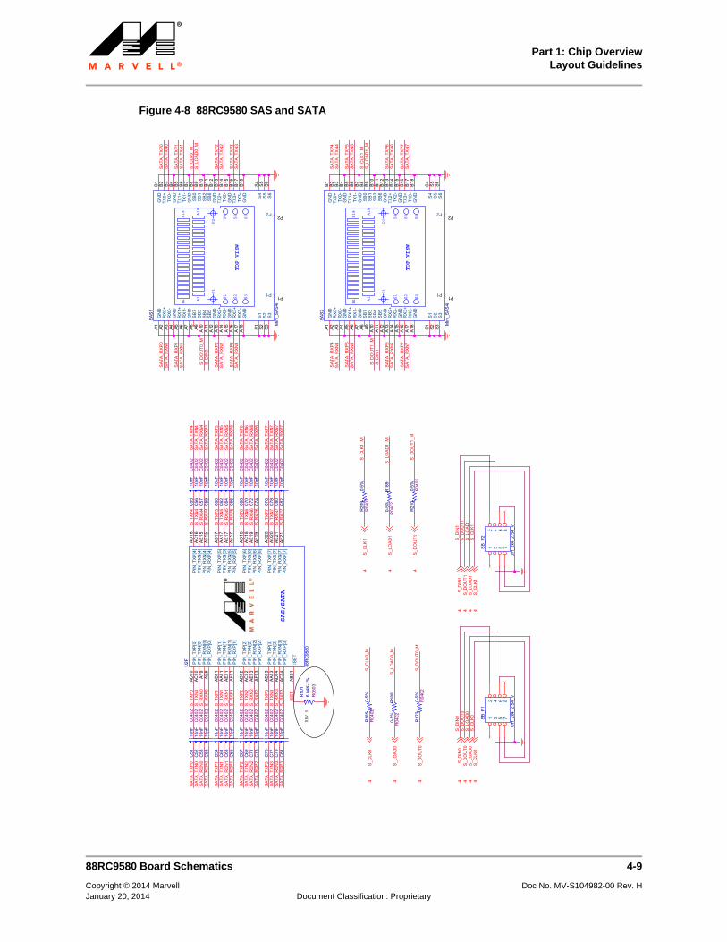
Part 1: Chip OverviewLayout Guidelines
88RC9580 Board Schematics 4-9
Copyright © 2014 Marvell Doc No. MV-S104982-00 Rev. HJanuary 20, 2014 Document Classification: Proprietary
Figure 4-8 88RC9580 SAS and SATA
REV
5
SATA
_TXN
7SA
TA_T
XP7
S_TX
N4
S_R
XP4
S_R
XN4
S_TX
N5
S_TX
P4
S_R
XN5
S_R
XP5
S_TX
P0S_
TXN
0
S_TX
P6S_
TXN
6
SATA
_RXP
3SA
TA_R
XN3
SATA
_RXP
4SA
TA_R
XN4
SATA
_RXP
5SA
TA_R
XN5
SATA
_TXN
0SA
TA_T
XP0
SATA
_RXP
6SA
TA_R
XN6
SATA
_TXP
1SA
TA_T
XN1
S_R
XP0
SATA
_RXP
7SA
TA_R
XN7
SATA
_TXP
2SA
TA_T
XN2
SATA
_TXP
3SA
TA_T
XN3
SATA
_TXP
4SA
TA_T
XN4
S_R
XN6
SATA
_RXP
0SA
TA_R
XN0
S_R
XP6
S_TX
P7S_
TXN
7S_
RXN
7S_
RXP
7
S_TX
P5SA
TA_T
XP5
SATA
_TXN
5
S_R
XN0
S_TX
P1S_
TXN
1
SATA
_TXN
6
SATA
_RXP
1SA
TA_R
XN1
S_R
XN1
S_R
XP1
SATA
_TXP
6S_
TXP2
S_TX
N2
SATA
_RXP
2SA
TA_R
XN2
S_R
XN2
S_R
XP2
S_TX
P3S_
TXN
3S_
RXN
3S_
RXP
3
SATA
_RXP
0SA
TA_R
XN0
SATA
_RXP
1SA
TA_R
XN1
SATA
_RXP
2SA
TA_R
XN2
SATA
_RXP
3SA
TA_R
XN3
SATA
_TXN
0SA
TA_T
XP0
SATA
_TXP
1SA
TA_T
XN1
SATA
_TXP
2SA
TA_T
XN2
SATA
_TXN
3SA
TA_T
XP3
S_C
LK0_
MS_
LOAD
0_M
S_D
OU
T0_M
S_D
IN0
S_LO
AD1_
MS_
CLK
1_M
S_D
IN1
S_D
OU
T1_M
SATA
_RXN
4SA
TA_R
XP4
SATA
_RXN
5SA
TA_R
XP5
SATA
_RXN
6SA
TA_R
XP6
SATA
_RXN
7SA
TA_R
XP7
SATA
_TXN
4SA
TA_T
XP4
SATA
_TXN
5SA
TA_T
XP5
SATA
_TXN
6SA
TA_T
XP6
SATA
_TXN
7SA
TA_T
XP7
S_D
OU
T0S_
DIN
0S_
DIN
1
S_LO
AD0
S_C
LK0
S_C
LK1
S_LO
AD1
S_D
OU
T1
S_C
LK0_
M
S_LO
AD0_
M
S_D
OU
T0_M
S_D
OU
T1_M
S_C
LK1_
M
S_LO
AD1_
M
ISET
S_C
LK0
4
S_LO
AD0
4
S_D
IN0
4S_
DO
UT0
4
S_C
LK0
4S_
LOAD
04
S_D
IN1
4S_
DO
UT1
4S_
LOAD
14
S_C
LK1
4
S_D
OU
T04
S_C
LK1
4
S_LO
AD1
4
S_D
OU
T14
C80
10nF
C04
02
C60
10nF
C04
02
R18
90-
5%R
0402
R20
90-
5%R
0402
B1B1
8 A18
A1
TOP VIEW
S1 S2 S3
S5 S6S4
P1P2
SAS2
Min
i_SA
S4i
GN
DA
1
RX0
+A
2
RX0
-A
3
GN
DA
4
RX1
+A
5
RX1
-A
6
GN
DA
7
SB
7A
8
SB
3A
9
SB
4A
10
SB
5A
11
GN
DA
12
RX2
+A
13
RX2
-A
14
GN
DA
15
RX3
+A
16
RX3
-A
17
GN
DA
18
S1
S1
S2
S2
S3
S3
GN
DB
1
TX0+
B2
TX0-
B3
GN
DB
4
TX1+
B5
TX1-
B6
GN
DB
7
SB
0B
8
SB
1B
9
SB
2B
10
SB
6B
11
GN
DB
12
TX2+
B13
TX2-
B14
GN
DB
15
TX3+
B16
TX3-
B17
GN
DB
18
S4
S4
S5
S5
S6
S6
P1P1
P2P2
SB_P
1
UH
_2x4
_2.5
4_V
12
34
56
78
R17
20-
5%R
0402
C82
10nF
C04
02SAS/SATA
88R
C95
80
U2F
PIN
_RXN
[4]
AE
15
PIN
_RXN
[5]
AE
17
PIN
_RXN
[6]
AE
19
PIN
_RXN
[7]
AE
21
PIN
_RXP
[4]
AF1
5
PIN
_RXP
[5]
AF1
7
PIN
_RXP
[6]
AF1
9
PIN
_RXP
[7]
AF2
1
PIN
_TXN
[4]
AC16
PIN
_TXN
[5]
AA
17
PIN
_TXN
[6]
AC18
PIN
_TXN
[7]
AD20
PIN
_TXP
[4]
AD16
PIN
_TXP
[5]
AB
17
PIN
_TXP
[6]
AD18
PIN
_TXP
[7]
AC20
PIN
_TXP
[0]
AD10
PIN
_TXN
[0]
AC10
PIN
_RXN
[0]
AF9
PIN
_RXP
[0]
AE
9
PIN
_TXP
[1]
AB
11
PIN
_TXN
[1]
AA
11
PIN
_RXN
[1]
AE
11
PIN
_RXP
[1]
AF1
1
PIN
_TXP
[2]
AD12
PIN
_TXN
[2]
AC12
PIN
_RXN
[2]
AE
13
PIN
_RXP
[2]
AF1
3
PIN
_TXP
[3]
AB
13
PIN
_TXN
[3]
AA
13
PIN
_RXN
[3]
AD14
PIN
_RXP
[3]
AC14
ISE
TA
B21
C57
10nF
C04
02
R21
00-
5%R
0402
C76
10nF
C04
02
C56
10nF
C04
02
C79
10nF
C04
02
R18
80-
5%R
0402
C61
10nF
C04
02
C78
10nF
C04
02
SB_P
2
UH
_2x4
_2.5
4_V
12
34
56
78
C59
10nF
C04
02
C81
10nF
C04
02
C63
10nF
C04
02
C55
10nF
C04
02
R18
50-
5%R
0402
C53
10nF
C04
02
C77
10nF
C04
02
C71
10nF
C04
02
C65
10nF
C04
02
R10
16.
04K-
1%R
0603
B1B1
8 A18
A1
TOP VIEW
S1 S2 S3
S5 S6S4
P1P2
SAS1
Min
i_SA
S4i
GN
DA
1
RX0
+A
2
RX0
-A
3
GN
DA
4
RX1
+A
5
RX1
-A
6
GN
DA
7
SB
7A
8
SB
3A
9
SB
4A
10
SB
5A
11
GN
DA
12
RX2
+A
13
RX2
-A
14
GN
DA
15
RX3
+A
16
RX3
-A
17
GN
DA
18
S1
S1
S2
S2
S3
S3
GN
DB
1
TX0+
B2
TX0-
B3
GN
DB
4
TX1+
B5
TX1-
B6
GN
DB
7
SB
0B
8
SB
1B
9
SB
2B
10
SB
6B
11
GN
DB
12
TX2+
B13
TX2-
B14
GN
DB
15
TX3+
B16
TX3-
B17
GN
DB
18
S4
S4
S5
S5
S6
S6
P1P1
P2P2
C72
10nF
C04
02
C52
10nF
C04
02
C75
10nF
C04
02
C54
10nF
C04
02
C69
10nF
C04
02
C74
10nF
C04
02
C62
10nF
C04
02
C58
10nF
C04
02
C73
10nF
C04
02
C70
10nF
C04
02
C51
10nF
C04
02
C64
10nF
C04
02
C67
10nF
C04
02C
6810
nFC
0402
C66
10nF
C04
02
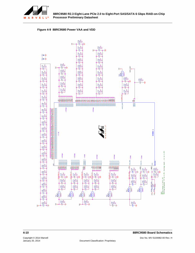
88RC9580 R2.3 Eight-Lane PCIe 2.0 to Eight-Port SAS/SATA 6 Gbps RAID-on-Chip Processor Preliminary Datasheet
4-10 88RC9580 Board Schematics
Copyright © 2014 Marvell Doc No. MV-S104982-00 Rev. HJanuary 20, 2014 Document Classification: Proprietary
Figure 4-9 88RC9580 Power VAA and VDD
VHV:
Efuse Power 2.5V/1.0V
[During program, it is 2.5V, During read , it is 1.0V]
~250mA
~3.5A
~400mA
~400mA
~400mA
~400mA
~10mA
~10mA
~800mA
~10mA
1V8_
AVD
D_4
-7
1V8_
AVD
D_0
-3
DR
R3_
PLL
2V5_
AVD
D_P
LL
2V5_
VAA_
PLL
VHV
2V5_
VAA_
ANA
2V5_
VAA_
4-7
2V5_
VAA_
0-3
1V0
3V3
1V5
1V5
1V5
1V0
2V5
2V5
1V8
DD
R3_
VREF
C13
310
0nF
C04
0210
V
R13
50-
5%R
0402
C91
10nF
C04
0216
V
C13
110
nFC
0402
16V
C11
610
uFC
0805
16V
C10
31n
FC
0402
50V
C15
410
0nF
C04
0210
V
C12
71u
FC
0402
10V
C98
1nF
C04
0250
V
C97
1nF
C04
0250
V
C90
10nF
C04
0216
V
C13
71n
FC
0402
50V
C10
910
nFC
0402
16V
C15
110
nFC
0402
16V
C12
910
uFC
0805
16V
C16
21n
FC
0402
50V
C14
210
nFC
0402
16VTP
16C
102
1nF
C04
0250
V
C12
810
uFC
0805
16V
C10
710
uFC
0805
16V
EMIF
IL(P2 GND)
FIL7
2200
pF
L080
5-3
C96
10nF
C04
0216
V
C11
01n
FC
0402
50V
C92
10nF
C04
0216
V
C11
510
0nF
C04
0210
V
EMIF
IL(P2 GND)
FIL1
2200
pF
L080
5-3
C15
210
0nF
C04
0210
V
C13
81n
FC
0402
50V
C86
100n
FC
0402
10V
C84
100n
FC
0402
10V
C15
910
0nF
C04
0210
V
TP17
C93
10nF
C04
0216
V
C10
810
0nF
C04
0210
V
C14
310
nFC
0402
16V
EMIF
IL(P2 GND)
FIL3
2200
pF
L080
5-3
C10
51n
FC
0402
50V
C13
010
0nF
C04
0210
V
C88
10nF
C04
0216
V
C14
710
nFC
0402
16V
EMIF
IL(P2 GND)
FIL6
2200
pF
L080
5-3
EMIF
IL(P2 GND)
FIL2
2200
pF
L080
5-3
C85
100n
FC
0402
10V
C11
21n
FC
0402
50V
C87
100n
FC
0402
10V
R13
4D
NP_
0-5%
R04
02
C11
910
0nF
C04
0210
V
C12
010
nFC
0402
16V
C14
410
nFC
0402
16V
C11
110
nFC
0402
16V
C14
610
0nF
C04
0210
V
C10
41n
FC
0402
50V
EMIF
IL(P2 GND)
FIL9
2200
pF
L080
5-3
C11
410
nFC
0402
16V
C13
91n
FC
0402
50V
EMIF
IL(P2 GND)
FIL5
2200
pF
L080
5-3
C10
11n
FC
0402
50V
C13
21n
FC
0402
50V
C12
110
nFC
0402
16V
C11
71n
FC
0402
50V
C89
10nF
C04
0216
V
C14
81n
FC
0402
50V
C12
410
0nF
C04
0210
V
POWER-1
88R
C95
80
U2G VA
A_0-
3Y9
VAA_
0-3
Y10
VAA_
0-3
Y11
VAA_
0-3
Y12
VAA_
0-3
Y13
VAA_
0-3
Y14
VAA_
0-3
AA9
VAA_
0-3
AB9
VAA_
4-7
Y15
VAA_
4-7
Y16
VAA_
4-7
Y17
VAA_
4-7
Y18
VAA_
4-7
AA15
VAA_
4-7
AA19
VAA_
4-7
AB15
VAA_
4-7
AB19
VAA_
ANA
Y19
VAA_
PLL
AA20
VHV
AB22
VREF
DF9
VREF
SD
9
AVD
D_0
-3G
16
AVD
D_0
-3G
17
AVD
D_0
-3G
18
AVD
D_0
-3H
15
AVD
D_0
-3H
16
AVD
D_0
-3H
17
AVD
D_0
-3H
18
AVD
D_4
-7G
11
AVD
D_4
-7G
12
AVD
D_4
-7G
13
AVD
D_4
-7H
10
AVD
D_4
-7H
11
AVD
D_4
-7H
12
AVD
D_4
-7H
13
AVD
D_D
DR
L1
AVD
D25
_0G
10
AVD
D25
_1D
23
VDDK9
VDDK11
VDDK13
VDDK15
VDDK17
VDDL10
VDDL12
VDDL14
VDDL16
VDDM9
VDDM11
VDDM13
VDDM15
VDDM17
VDDN10
VDDN12
VDDN14
VDDN16
VDDP9
VDDP11
VDDP13
VDDP15
VDDP17
VDDR10
VDDR12
VDDR14
VDDR16
VDDT9
VDDT11
VDDT13
VDDT15
VDDT17
VDDU10
VDDU12
VDDU14
VDDU16
VDDV9
VDDV11
VDDV13
VDDV15
VDDV17
VDD
O1
J18
VDD
O1
K18
VDD
O1
L18
VDD
O1
M18
VDD
O1
N18
VDD
O1
P18
VDD
O1
P19
VDD
O1
R18
VDD
O1
T18
VDD
O1
U18
VDD
O1
V18
VDD
O1
W18
VDD
QB4
VDD
QB8
VDD
QD
4
VDD
QD
8
VDD
QF4
VDD
QF8
VDD
QG
7
VDD
QH
4
VDD
QH
7
VDD
QJ7
VDD
QK4
VDD
QK7
VDD
QL7
VDD
QM
4
VDD
QM
7
VDD
QN
7
VDD
QP4
VDD
QP7
VDD
QR
7
VDD
QT4
VDD
QT7
VDD
QU
7
VDD
QV4
VDD
QV7
VDD
QW
7
VDD
QY4
VDD
QY7
VDD
QAB
4
VDD
QAB
8
VDD
QAD
4
VDD
QAD
8
VDD
QAF
4
C14
01n
FC
0402
50V
C10
01n
FC
0402
50V
C12
210
0nF
C04
0210
V
C11
810
0nF
C04
0210
V
C16
010
0nF
C04
0210
VC13
410
nFC
0402
16V
C14
510
uFC
0805
16V
C16
410
0nF
C04
0210
V
C15
61n
FC
0402
50V
C12
510
0nF
C04
0210
V
C83
10uF
C08
0516
V
EMIF
IL(P2 GND)
FIL4
2200
pF
L080
5-3
C95
10nF
C04
0216
V
C13
51n
FC
0402
50V
C16
110
nFC
0402
16V
C12
310
0nF
C04
0210
V
C12
61u
FC
0402
10V
C15
510
nFC
0402
16V
C15
310
uFC
0805
16V
C15
01n
FC
0402
50V
C16
31u
FC
0603
6V3
C99
1nF
C04
0250
V
C14
11n
FC
0402
50V
C94
10nF
C04
0216
V

Part 1: Chip OverviewLayout Guidelines
88RC9580 Board Schematics 4-11
Copyright © 2014 Marvell Doc No. MV-S104982-00 Rev. HJanuary 20, 2014 Document Classification: Proprietary
Figure 4-10 88RC9580 Power Ground
POWER-2
88RC9580
U2H
VSSA1
VSSA6
VSSA10
VSSA12
VSSA14
VSSA16
VSSA18
VSSA20
VSSA22
VSSA24
VSSA26
VSSB10
VSSB12
VSSB14
VSSB16
VSSB18
VSSB20
VSSB22
VSSB24
VSSC2
VSSC6
VSSC11
VSSC13
VSSC15
VSSC17
VSSC19
VSSC21
VSSC23
VSSD11
VSSD13
VSSD15
VSSD17
VSSD19
VSSD21
VSSE2
VSSE6
VSSE10
VSSE12
VSSE14
VSSE16
VSSE18
VSSE20
VSSF10
VSSF12
VSSF14
VSSF16
VSSF18
VS
SF2
0
VS
SG
2
VS
SG
6
VS
SG
8
VS
SG
9
VS
SG
15
VS
SG
19
VS
SH
8
VS
SH
9
VS
SJ2
VS
SJ6
VS
SJ8
VS
SJ9
VS
SJ1
0
VS
SJ1
1
VS
SJ1
2
VS
SJ1
3
VS
SJ1
4
VS
SJ1
5
VS
SJ1
6
VS
SJ1
7
VS
SK
8
VS
SK
10
VS
SK
12
VS
SK
14
VS
SK
16
VS
SL2
VS
SL6
VS
SL8
VS
SL9
VS
SL1
1
VS
SL1
3
VS
SL1
5
VS
SL1
7
VS
SM
8
VS
SM
10
VS
SM
12
VS
SM
14
VS
SM
16
VS
SN
2
VS
SN
6
VS
SN
8
VS
SN
9
VS
SN
11
VS
SN
13VSS
N15VSSN17VSSP8VSSP10VSSP12VSSP14VSSP16VSSR2VSSR6VSSR8VSSR9VSSR11VSSR13VSSR15VSSR17VSST8VSST10VSST12VSST14VSST16VSSU3VSSU6VSSU8VSSU9VSSU11VSSU13VSSU15VSSU17VSSV8VSSV10VSSV12VSSV14VSSV16VSSW2VSSW6VSSW8VSSW9VSSW10VSSW11VSSW12VSSW13VSSW14VSSW15VSSW16VSSW17VSSY8VSSAA2V
SS
AA
6V
SS
AA
10V
SS
AA
12V
SS
AA
14V
SS
AA
16V
SS
AA
18V
SS
AB
10V
SS
AB
12V
SS
AB
14V
SS
AB
16V
SS
AB
18V
SS
AB
20V
SS
AC
2V
SS
AC
6V
SS
AC
9V
SS
AC
11V
SS
AC
13V
SS
AC
15V
SS
AC
17V
SS
AC
19V
SS
AC
21V
SS
AD
9V
SS
AD
11V
SS
AD
13V
SS
AD
15V
SS
AD
17V
SS
AD
19V
SS
AD
21V
SS
AE
2V
SS
AE
6V
SS
AE
8V
SS
AE
10V
SS
AE
12V
SS
AE
14V
SS
AE
16V
SS
AE
18V
SS
AE
20V
SS
AE
22V
SS
AF1
VS
SA
F8V
SS
AF1
0V
SS
AF1
2V
SS
AF1
4V
SS
AF1
6V
SS
AF1
8V
SS
AF2
0V
SS
AF2
2V
SS
AF2
6

88RC9580 R2.3 Eight-Lane PCIe 2.0 to Eight-Port SAS/SATA 6 Gbps RAID-on-Chip Processor Preliminary Datasheet
4-12 88RC9580 Board Schematics
Copyright © 2014 Marvell Doc No. MV-S104982-00 Rev. HJanuary 20, 2014 Document Classification: Proprietary
Figure 4-11 88RC9580 DDR3 CHIPS
REV 5
REV 5
REV 5
REV 5
REV 5
DD
R3_
RAS
#
DD
R3_
CLK
0
DD
R3_
A6
DD
R3_
A8
DD
R3_
A0D
DR
3_A1
DD
R3_
A12
DD
R3_
A5
DD
R3_
A10
DD
R3_
A2
DD
R3_
A9
DD
R3_
A11
DD
R3_
A3D
DR
3_A4
DD
R3_
A7
DD
R3_
DQ
30D
DR
3_D
Q29
DD
R3_
DQ
28D
DR
3_D
Q27
DD
R3_
DQ
26D
DR
3_D
Q25
DD
R3_
DQ
24
DD
R3_
DQ
31
DD
R3_
CLK
#0
DD
R3_
A12
DD
R3_
A7
DD
R3_
A2
DD
R3_
BA2
DD
R3_
A6
DD
R3_
DQ
S#2
DD
R3_
DQ
S2D
DR
3_D
M2
DD
R3_
DM
3
DD
R3_
DQ
22D
DR
3_D
Q23
DD
R3_
DQ
21D
DR
3_D
Q20
DD
R3_
DQ
19D
DR
3_D
Q18
DD
R3_
DQ
17D
DR
3_D
Q16
DD
R3_
DQ
S3D
DR
3_D
QS#
3
DD
R3_
BA0
DD
R3_
BA2
DD
R3_
BA1
DD
R3_
A6
DD
R3_
A8
DD
R3_
A0D
DR
3_A1
DD
R3_
A12
DD
R3_
A5
DD
R3_
A10
DD
R3_
A2
DD
R3_
A9
DD
R3_
A11
DD
R3_
A3D
DR
3_A4
DD
R3_
A7
DD
R3_
DQ
46D
DR
3_D
Q45
DD
R3_
DQ
44D
DR
3_D
Q43
DD
R3_
DQ
42D
DR
3_D
Q41
DD
R3_
DQ
40
DD
R3_
DQ
47
DD
R3_
DQ
S#4
DD
R3_
DQ
S4D
DR
3_D
M4
DD
R3_
DM
5
DD
R3_
DQ
38D
DR
3_D
Q39
DD
R3_
DQ
37D
DR
3_D
Q36
DD
R3_
DQ
35D
DR
3_D
Q34
DD
R3_
DQ
33D
DR
3_D
Q32
DD
R3_
DQ
S5D
DR
3_D
QS#
5
DD
R3_
BA0
DD
R3_
BA2
DD
R3_
BA1
DD
R3_
A6
DD
R3_
A8
DD
R3_
A0D
DR
3_A1
DD
R3_
A12
DD
R3_
A5
DD
R3_
A10
DD
R3_
A2
DD
R3_
A9
DD
R3_
A11
DD
R3_
A3D
DR
3_A4
DD
R3_
A7
DD
R3_
DQ
62D
DR
3_D
Q61
DD
R3_
DQ
60D
DR
3_D
Q59
DD
R3_
DQ
58D
DR
3_D
Q57
DD
R3_
DQ
56
DD
R3_
DQ
63
DD
R3_
DQ
S#6
DD
R3_
DQ
S6D
DR
3_D
M6
DD
R3_
DM
7
DD
R3_
DQ
54D
DR
3_D
Q55
DD
R3_
DQ
53D
DR
3_D
Q52
DD
R3_
DQ
51D
DR
3_D
Q50
DD
R3_
DQ
49D
DR
3_D
Q48
DD
R3_
DQ
S7D
DR
3_D
QS#
7
DD
R3_
BA0
DD
R3_
BA2
DD
R3_
BA1
SDR
AM_C
KE0
DD
R3_
A6
DD
R3_
A8
DD
R3_
A0D
DR
3_A1
DD
R3_
A12
DD
R3_
A5
DD
R3_
A10
DD
R3_
A2
DD
R3_
A9
DD
R3_
A11
DD
R3_
A3D
DR
3_A4
DD
R3_
A7
DD
R3_
WE#
DD
R3_
A10
DD
R3_
A13
DD
R3_
A9
DD
R3_
A8
DD
R3_
A3
DD
R3_
A5
DD
R3_
BA0
DD
R3_
A11
DD
R3_
CLK
0
DD
R3_
A6
DD
R3_
A8
DD
R3_
A0D
DR
3_A1
DD
R3_
A12
DD
R3_
A5
DD
R3_
A10
DD
R3_
A2
DD
R3_
A9
DD
R3_
A11
DD
R3_
A3
DD
R3_
BA0
DD
R3_
A4
DD
R3_
A7
DD
R3_
BA2
DD
R3_
BA1
DD
R3_
DQ
14D
DR
3_D
Q13
DD
R3_
DQ
12D
DR
3_D
Q11
DD
R3_
DQ
10D
DR
3_D
Q9
DD
R3_
DQ
8
DD
R3_
DQ
15
DD
R3_
DQ
S#0
DD
R3_
DQ
S0D
DR
3_D
M0
DD
R3_
A1D
DR
3_BA
1
DD
R3_
A4
DD
R3_
DM
1
DD
R3_
DQ
6D
DR
3_D
Q7
DD
R3_
DQ
5D
DR
3_D
Q4
DD
R3_
DQ
3D
DR
3_D
Q2
DD
R3_
DQ
1D
DR
3_D
Q0
DD
R3_
DQ
S1D
DR
3_D
QS#
1
DD
R3_
BA0
DD
R3_
BA2
DD
R3_
BA1
SDR
AM_C
SN0
DD
R3_
CLK
#0
DD
R3_
CBS
#D
DR
3_C
BSD
DR
3_C
BM
DD
R3_
CB6
DD
R3_
CB7
DD
R3_
CB5
DD
R3_
CB4
DD
R3_
CB3
DD
R3_
CB2
DD
R3_
CB1
DD
R3_
CB0
DD
R3_
A13
SDR
AM_C
SN0
SDR
AM_C
KE0
SDR
AM_O
DT0
DD
R3_
CAS
#D
DR
3_R
AS#
DD
R3_
WE#
DD
R3_
RES
ET#
DD
R3_
A13
DD
R3_
RES
ET#
SDR
AM_C
KE0
SDR
AM_C
SN0
SDR
AM_O
DT0
DD
R3_
CAS
#D
DR
3_W
E#
DD
R3_
RAS
#
DD
R3_
A13
SDR
AM_C
SN0
DD
R3_
RES
ET#
SDR
AM_O
DT0
DD
R3_
CAS
#D
DR
3_R
AS#
DD
R3_
WE#
SDR
AM_C
KE0
DD
R3_
A13
SDR
AM_O
DT0
DD
R3_
CAS
#D
DR
3_R
AS#
DD
R3_
WE#
DD
R3_
RES
ET#
SDR
AM_C
SN0
SDR
AM_C
KE0
DD
R3_
A13
DD
R3_
CAS
#
SDR
AM_O
DT0
DD
R3_
RAS
#
DD
R3_
WE#
DD
R3_
RES
ET#
SDR
AM_C
SN0
DD
R3_
A0
DD
R3_
CAS
#
DD
R3_
CLK
1D
DR
3_C
LK#1
SDR
AM_C
KE0
SDR
AM_O
DT0
DD
R3_
CLK
1D
DR
3_C
LK#1
DD
R3_
CLK
#2D
DR
3_C
LK2
DD
R3_
VREF
CA
DD
R3_
VREF
CA
DD
R3_
VREF
CA
DD
R3_
VREF
CA
DD
R3_
VREF
CA
DD
R3_
VREF
CA
DD
R3_
VTT
1V5_
DD
R3
DD
R3_
VTT
1V5_
DD
R3
1V5_
DD
R3
1V5_
DD
R3
1V5_
DD
R3
1V5_
DD
R3
1V5_
DD
R3
1V5_
DD
R3
1V5_
DD
R3
1V5_
DD
R3
1V5_
DD
R3
1V5_
DD
R3
DD
R3_
VREF
DD
R3_
VREF
DD
R3_
VREF
DD
R3_
VREF
DD
R3_
VREF
DD
R3_
DQ
[63.
.0]
7
DD
R3_
RAS
#7
DD
R3_
DQ
S57
DD
R3_
DM
57
DD
R3_
DQ
S#5
7
SDR
AM_C
SN0
7
DD
R3_
DM
67
DD
R3_
DQ
S67
DD
R3_
DQ
S#6
7
DD
R3_
BA[2
..0]
7
DD
R3_
DQ
S#7
7D
DR
3_D
QS7
7
DD
R3_
CBS
#7
DD
R3_
CLK
07
DD
R3_
CLK
#07
SDR
AM_O
DT0
7
DD
R3_
DQ
S#0
7
DD
R3_
WE#
7
DD
R3_
A[13
..0]
7D
DR
3_C
B[7.
.0]
7
DD
R3_
CAS
#7
DD
R3_
DM
[7..0
]7
DD
R3_
DQ
S#1
7D
DR
3_D
QS1
7D
DR
3_D
M1
7D
DR
3_D
QS#
27
DD
R3_
DM
27
DD
R3_
DQ
S27
DD
R3_
CBS
7
DD
R3_
DQ
S07
DD
R3_
DQ
S#3
7D
DR
3_D
QS3
7D
DR
3_D
M3
7
DD
R3_
CBM
7
SDR
AM_C
KE0
7
DD
R3_
RES
ET#
7
DD
R3_
DM
07
DD
R3_
DM
47
DD
R3_
DQ
S47
DD
R3_
DQ
S#4
7
DD
R3_
CLK
17
DD
R3_
CLK
#17
DD
R3_
CLK
#27
DD
R3_
CLK
27
C21
71n
FC
0402
50V
R21
210
0-1%
R04
02
C18
410
uFC
0805
16V
R13
624
0-1%
R04
02
C20
110
0nF
C04
0210
V
C22
510
nFC
0402
16V
C16
510
0nF
C04
0210
V
C18
510
0nF
C04
0210
V
C20
410
nFC
0402
16V
C21
510
nFC
0402
16V
U15
MT4
1J64
M16
LA-1
5E
BA2
M3
BA1
N8
BA0
M2
A12/
BCN
7
A11
R7
A10/
APL7
A9R
3
A8T8
A7R
2
A6R
8
A5P2
A4P8
A3N
2
A2P3
A1P7
A0N
3
CLK
J7
CLK
K7
CKE
K9
CS
L2
OD
TK1
RAS
J3
CAS
K3
WE
L3
VDD
1B2
VDD
2D
9
VDD
3G
7
VDD
4K2
VDD
Q5
D2
VDD
Q4
C9
VDD
Q3
C1
VDD
Q2
A8VD
DQ
1A1
VREF
CA
M8
VSSQ
1B1
VSSQ
2B9
VSSQ
3D
1
VSSQ
4D
8
VSSQ
5E2
VDD
5K8
VDD
Q9
H9
VDD
Q8
H2
VDD
Q7
F1VD
DQ
6E9
VSS1
A9
VSS2
B3
VSS3
E1
VSS4
G8
VSS5
J2
VSSQ
6E8
VSSQ
7F9
VSSQ
8G
1
VSSQ
9G
9
NC
1J1
NC
2J9
DQ
U7
A3
DQ
U6
B8
DQ
U5
A2
DQ
U4
A7
DQ
U3
C2
DQ
U2
C8
DQ
U1
C3
DQ
U0
D7
DQ
SLG
3
DQ
SLF3
DM
LE7
DQ
L0E3
DQ
L1F7
DQ
L2F2
DQ
L3F8
DQ
L4H
3D
QL5
H8
DQ
SUB7
DQ
SUC
7
DM
UD
3
DQ
L7H
7
DQ
L6G
2
RES
ETT2
VDD
6N
1
VDD
7N
9
VDD
8R
1
VDD
9R
9
VREF
DQ
H1
VSS6
J8
VSS7
M1
VSS8
M9
VSS9
P1
VSS1
0P9
VSS1
1T1
VSS1
2T9
ZQL8
NC
3L1
NC
4L9
NC
5M
7
A13
T3
NC
6T7
R13
924
0-1%
R04
02
C28
31u
FC
0402
10V
C22
110
0nF
C04
0210
V
TP20
C18
710
nFC
0402
16V
C21
210
0nF
C04
0210
V
R20
030
0-1%
R04
02
C20
510
nFC
0402
16V
R14
1D
NP_
49.9
-1%
R04
02
C19
510
nFC
0402
16V
U17
MT4
1J64
M16
LA-1
5E
BA2
M3
BA1
N8
BA0
M2
A12/
BCN
7
A11
R7
A10/
APL7
A9R
3
A8T8
A7R
2
A6R
8
A5P2
A4P8
A3N
2
A2P3
A1P7
A0N
3
CLK
J7
CLK
K7
CKE
K9
CS
L2
OD
TK1
RAS
J3
CAS
K3
WE
L3
VDD
1B2
VDD
2D
9
VDD
3G
7
VDD
4K2
VDD
Q5
D2
VDD
Q4
C9
VDD
Q3
C1
VDD
Q2
A8VD
DQ
1A1
VREF
CA
M8
VSSQ
1B1
VSSQ
2B9
VSSQ
3D
1
VSSQ
4D
8
VSSQ
5E2
VDD
5K8
VDD
Q9
H9
VDD
Q8
H2
VDD
Q7
F1VD
DQ
6E9
VSS1
A9
VSS2
B3
VSS3
E1
VSS4
G8
VSS5
J2
VSSQ
6E8
VSSQ
7F9
VSSQ
8G
1
VSSQ
9G
9
NC
1J1
NC
2J9
DQ
U7
A3
DQ
U6
B8
DQ
U5
A2
DQ
U4
A7
DQ
U3
C2
DQ
U2
C8
DQ
U1
C3
DQ
U0
D7
DQ
SLG
3
DQ
SLF3
DM
LE7
DQ
L0E3
DQ
L1F7
DQ
L2F2
DQ
L3F8
DQ
L4H
3D
QL5
H8
DQ
SUB7
DQ
SUC
7
DM
UD
3
DQ
L7H
7
DQ
L6G
2
RES
ETT2
VDD
6N
1
VDD
7N
9
VDD
8R
1
VDD
9R
9
VREF
DQ
H1
VSS6
J8
VSS7
M1
VSS8
M9
VSS9
P1
VSS1
0P9
VSS1
1T1
VSS1
2T9
ZQL8
NC
3L1
NC
4L9
NC
5M
7
A13
T3
NC
6T7
RN
349
.9-1
%R
A060
3
1 2 3 45678
C17
810
nFC
0402
16V
C28
410
uFC
0805
16V
RN
449
.9-1
%R
A060
3
1 2 3 45678
RN
249
.9-1
%R
A060
3
1 2 3 45678
C28
61n
FC
0402
50V
C19
21n
FC
0402
50V
C18
810
nFC
0402
16V
R14
224
0-1%
R04
02
C21
910
uFC
0805
16V
U19
MT4
1J64
M16
LA-1
5E
BA2
M3
BA1
N8
BA0
M2
A12/
BCN
7
A11
R7
A10/
APL7
A9R
3
A8T8
A7R
2
A6R
8
A5P2
A4P8
A3N
2
A2P3
A1P7
A0N
3
CLK
J7
CLK
K7
CKE
K9
CS
L2
OD
TK1
RAS
J3
CAS
K3
WE
L3
VDD
1B2
VDD
2D
9
VDD
3G
7
VDD
4K2
VDD
Q5
D2
VDD
Q4
C9
VDD
Q3
C1
VDD
Q2
A8VD
DQ
1A1
VREF
CA
M8
VSSQ
1B1
VSSQ
2B9
VSSQ
3D
1
VSSQ
4D
8
VSSQ
5E2
VDD
5K8
VDD
Q9
H9
VDD
Q8
H2
VDD
Q7
F1VD
DQ
6E9
VSS1
A9
VSS2
B3
VSS3
E1
VSS4
G8
VSS5
J2
VSSQ
6E8
VSSQ
7F9
VSSQ
8G
1
VSSQ
9G
9
NC
1J1
NC
2J9
DQ
U7
A3
DQ
U6
B8
DQ
U5
A2
DQ
U4
A7
DQ
U3
C2
DQ
U2
C8
DQ
U1
C3
DQ
U0
D7
DQ
SLG
3
DQ
SLF3
DM
LE7
DQ
L0E3
DQ
L1F7
DQ
L2F2
DQ
L3F8
DQ
L4H
3D
QL5
H8
DQ
SUB7
DQ
SUC
7
DM
UD
3
DQ
L7H
7
DQ
L6G
2
RES
ETT2
VDD
6N
1
VDD
7N
9
VDD
8R
1
VDD
9R
9
VREF
DQ
H1
VSS6
J8
VSS7
M1
VSS8
M9
VSS9
P1
VSS1
0P9
VSS1
1T1
VSS1
2T9
ZQL8
NC
3L1
NC
4L9
NC
5M
7
A13
T3
NC
6T7
C21
610
nFC
0402
16VR
138
240-
1%R
0402
C19
910
uFC
0805
16V
U18
MT4
1J64
M16
LA-1
5E
BA2
M3
BA1
N8
BA0
M2
A12/
BCN
7
A11
R7
A10/
APL7
A9R
3
A8T8
A7R
2
A6R
8
A5P2
A4P8
A3N
2
A2P3
A1P7
A0N
3
CLK
J7
CLK
K7
CKE
K9
CS
L2
OD
TK1
RAS
J3
CAS
K3
WE
L3
VDD
1B2
VDD
2D
9
VDD
3G
7
VDD
4K2
VDD
Q5
D2
VDD
Q4
C9
VDD
Q3
C1
VDD
Q2
A8VD
DQ
1A1
VREF
CA
M8
VSSQ
1B1
VSSQ
2B9
VSSQ
3D
1
VSSQ
4D
8
VSSQ
5E2
VDD
5K8
VDD
Q9
H9
VDD
Q8
H2
VDD
Q7
F1VD
DQ
6E9
VSS1
A9
VSS2
B3
VSS3
E1
VSS4
G8
VSS5
J2
VSSQ
6E8
VSSQ
7F9
VSSQ
8G
1
VSSQ
9G
9
NC
1J1
NC
2J9
DQ
U7
A3
DQ
U6
B8
DQ
U5
A2
DQ
U4
A7
DQ
U3
C2
DQ
U2
C8
DQ
U1
C3
DQ
U0
D7
DQ
SLG
3
DQ
SLF3
DM
LE7
DQ
L0E3
DQ
L1F7
DQ
L2F2
DQ
L3F8
DQ
L4H
3D
QL5
H8
DQ
SUB7
DQ
SUC
7
DM
UD
3
DQ
L7H
7
DQ
L6G
2
RES
ETT2
VDD
6N
1
VDD
7N
9
VDD
8R
1
VDD
9R
9
VREF
DQ
H1
VSS6
J8
VSS7
M1
VSS8
M9
VSS9
P1
VSS1
0P9
VSS1
1T1
VSS1
2T9
ZQL8
NC
3L1
NC
4L9
NC
5M
7
A13
T3
NC
6T7
C17
910
nFC
0402
16V
RN
149
.9-1
%R
A060
3
1 2 3 45678
R20
449
.9-1
%R
0402
C22
310
nFC
0402
16V
C23
010
0nF
C04
0210
V
C16
910
0nF
C04
0210
V
C16
810
0nF
C04
0210
V
C19
31n
FC
0402
50V
U16
MT4
1J64
M16
LA-1
5E
BA2
M3
BA1
N8
BA0
M2
A12/
BCN
7
A11
R7
A10/
APL7
A9R
3
A8T8
A7R
2
A6R
8
A5P2
A4P8
A3N
2
A2P3
A1P7
A0N
3
CLK
J7
CLK
K7
CKE
K9
CS
L2
OD
TK1
RAS
J3
CAS
K3
WE
L3
VDD
1B2
VDD
2D
9
VDD
3G
7
VDD
4K2
VDD
Q5
D2
VDD
Q4
C9
VDD
Q3
C1
VDD
Q2
A8VD
DQ
1A1
VREF
CA
M8
VSSQ
1B1
VSSQ
2B9
VSSQ
3D
1
VSSQ
4D
8
VSSQ
5E2
VDD
5K8
VDD
Q9
H9
VDD
Q8
H2
VDD
Q7
F1VD
DQ
6E9
VSS1
A9
VSS2
B3
VSS3
E1
VSS4
G8
VSS5
J2
VSSQ
6E8
VSSQ
7F9
VSSQ
8G
1
VSSQ
9G
9
NC
1J1
NC
2J9
DQ
U7
A3
DQ
U6
B8
DQ
U5
A2
DQ
U4
A7
DQ
U3
C2
DQ
U2
C8
DQ
U1
C3
DQ
U0
D7
DQ
SLG
3
DQ
SLF3
DM
LE7
DQ
L0E3
DQ
L1F7
DQ
L2F2
DQ
L3F8
DQ
L4H
3D
QL5
H8
DQ
SUB7
DQ
SUC
7
DM
UD
3
DQ
L7H
7
DQ
L6G
2
RES
ETT2
VDD
6N
1
VDD
7N
9
VDD
8R
1
VDD
9R
9
VREF
DQ
H1
VSS6
J8
VSS7
M1
VSS8
M9
VSS9
P1
VSS1
0P9
VSS1
1T1
VSS1
2T9
ZQL8
NC
3L1
NC
4L9
NC
5M
7
A13
T3
NC
6T7
C21
010
uFC
0805
16V
C20
010
0nF
C04
0210
V
C17
010
0nF
C04
0210
V
C19
610
0nF
C04
0210
V
RN
549
.9-1
%R
A060
3
1 2 3 45678
C17
210
0nF
C04
0210
V
C22
210
nFC
0402
16V
C22
71n
FC
0402
50V
R13
724
0-1%
R04
02
C18
610
0nF
C04
0210
V
TP24
C19
710
0nF
C04
0210
V
C16
610
0nF
C04
0210
V
C21
410
nFC
0402
16V
C20
310
nFC
0402
16V
C17
310
uFC
0805
16V
C17
510
0nF
C04
0210
V
C17
410
0nF
C04
0210
V
C29
3D
NP_
47uF
C08
056V
3
C28
710
nFC
0402
16V
C17
610
nFC
0402
16V
C22
010
0nF
C04
0210
V
C18
910
nFC
0402
16V
R28
410
K-5%
R04
02
C20
71n
FC
0402
50V
C20
210
nFC
0402
16V
C22
61n
FC
0402
50V
TP34
C21
110
0nF
C04
0210
V
R14
049
.9-1
%R
0402
C29
4D
NP_
47uF
C08
056V
3
C18
01n
FC
0402
50V
C20
91n
FC
0402
50V
TP35
C21
81n
FC
0402
50V
C20
81n
FC
0402
50V
C17
710
nFC
0402
16V
R21
110
0-1%
R04
02
C19
81n
FC
0402
50V
C19
010
nFC
0402
16V
C18
210
0nF
C04
0210
V
C20
61n
FC
0402
50V
C21
310
nFC
0402
16V
TP27
C19
410
nFC
0402
16V
TP26
C17
110
0nF
C04
0210
V
C16
710
0nF
C04
0210
V
C18
11n
FC
0402
50V
C19
110
nFC
0402
16V
C22
410
nFC
0402
16V
C18
310
0nF
C04
0210
V

Part 1: Chip OverviewLayout Guidelines
88RC9580 Board Schematics 4-13
Copyright © 2014 Marvell Doc No. MV-S104982-00 Rev. HJanuary 20, 2014 Document Classification: Proprietary
Figure 4-12 88RC9580 System BKUP Power
5V TO 2.5V
354GPIO2
* Reverse and Cross-Conduction Blocking
* PWR_Switch_CTL=0, DISABLE BATTERY OUTPUT
PWR_Switch_CTL=1, AUTOSWITCH MODE
Latch EN
Charger_EN#
NAPWR Switch IC, D1
CHARGER_EN#
PULL HIGH AT RESET
BKUP BAT SOCKET
5V
to 1.5V and 1.8V
Imax=4A
1.157V
fsw=500KHz
Imax=4A
R03
R03
TC7343 and TC3528 combination
REV 5 external power for BBU testing
3850_P2_S-R
3850_P1_S-R
Current BBU has BAT1 pin[10:7]pull up to VBATT(4.2 volt)
Need level shifter between 88RC9580 and BAT pin [10:7]
SDA_
1SC
L_1
Pow
er_s
witc
h_Q
1
Cha
rger
_EN
#La
tch_
ENPW
R_S
witc
h_C
TL
POR
88PG
847_
2V5
8226
_SW
_1
8226
_SW
_2
SDI
POR
POR
3850
_P2_
S+
ITH
1
3850
_P1_
VFB
ILIM
SS1
SS2
3850
_BS2
3850
_SW
1
FREQ
3850
_BS1
LTC
3850
_VIN
3850
_TG
2
3850
_SW
2
3850
_BG
2
3850
_TG
1
ITH
2
RU
N2
MO
DE
3850
_BG
1
3850
_P2_
VFB
RU
N1
3850
_P2_
S+R
3850
_P1_
S+R
3850
_SW
2
3850
_P2_
S-
3850
_P1_
S-
3850
_P1_
S+
5V0
3V3
1V0
2V5
5V0
1V5
1V8
5V0 5V
0
5V0
3V3
5V0
PMU
X_O
UT
5V0
2V5
1V81V
5
2V5
PCIE
_12V
PCIE
_12V
LTC
3850
_SG
ND
PCIE
_12V
INTV
CC
LTC
3850
_SG
ND
INTV
CC
INTV
CC
INTV
CC
INTV
CC
5V0
5V0
1V0
Latc
h_EN
4PWR
_Sw
itch_
CTL
4
Cha
rger
_EN
#4
SCL_
13
SDA_
13
POR
3,13
Pow
er_s
witc
h_Q
14
POR
3,13
C25
2D
NP_
1000
pFC
0402
50V
C25
310
nFC
0402
16V
J1 DN
P_BP
_BLA
CK
L14.
7uH
10A
R18
397
.6K-
1%R
0402
R17
616
5K-1
%R
0402
GD S
Q2
FDS8
817N
Z
3
12
5678
4
R20
50-
5%R
0805
R165 4.7K-5%R0402
+
LED
2G
REE
N
R16
220
K-1%
R04
02
C26
7D
NP_
270p
FC
0402
50V
C22
810
uFC
0805
16V
C23
710
0PF
C04
0250
V
C25
622
uFC
0805
6V3
R18
20-
5%R
0402
R16
03.
01K-
1%R
0402
R166 4.7K-5%R0402
L8 3.3u
H1.
59A
R15
810
K-1%
R04
02
R10
510
-5%
R04
02
C22
910
0nF
C06
0325
V
JP10
DN
P_U
H_2
x1_2
.54
1
2
JP9
DN
P_U
H_2
x1_2
.54
1
2
R168 4.7K-5%R0402
R26
60-
5%R
0805
D2
B053
0WS
R17
70-
5%R
0402
R17
453
.6K-
1%R
0402
R170 4.7K-5%R0402
C29
110
0nF
C04
0210
V
R14
5
0.01
-1%
R08
05
C24
222
00pF
C04
0250
V
+C
250
150u
FTC
7343
6V3
XJP1
1D
NP_
SHU
NT
R15
40-
5%R
0402
R171 4.7K-5%R0402
NORMAL:3A
PEAK:4.5A
U22
88PG
847B
ILIM1
LDR2
SFB
3
CG
4
SW
15
PG
ND
6
SW
27
PVIN8
LFB
16
PS
ET
15V
SE
T14
SG
ND
13S
DI
12S
HD
N11
PO
R10
SV
IN9
L7 3.3u
H1.
59A
R14
310
-5%
R06
03
L21.
0uH
7.7A
R17
30-
5%R
0402
R15
90-
5%R
0603
JP11
DN
P_U
H_2
x1_2
.54
1
2
GD S
Q3
FDS8
817N
Z
3
12
5678
4
C26
022
uFC
0805
6V3
R18
60-
5%R
0805
C25
922
uFC
0805
6V3
C24
7D
NP_
470p
FC
0402
50V
R16
110
-1%
R06
03
R15
05.
11K-
1%R
0402
C25
110
nFC
0402
16V
R14
722
.1K-
1%R
0402
C24
822
uFC
0805
6V3
+C
295
150u
FTC
7343
6V3
SGND
(29)
U20
LTC
3850
TK
/SS
11
ITH
12
VFB
13
VFB
24
ITH
25
TK
/SS
26
SE
NS
E2-
7S
EN
SE
2+8
RU
N2
9
ILIM
10
EX
TV
CC
11
PG
OO
D12
SW
213
TG
214
BO
OS
T2
15
PG
ND
16
BG
217
INT
VC
C18
VIN
19
BG
120
BO
OS
T1
21
TG
122
SW
123
MO
DE
/PLL
IN24
FRE
Q/P
LLFL
TR
25
RU
N1
26
SE
NS
E1+
27
SE
NS
E1-
28
SG
ND
29
R18
71K
-5%
R04
02
R18
10-
5%R
0402
C26
122
uFC
0805
6V3
R15
5
0.01
-1%
R08
05
R17
90-
5%R
0402
+C
268
150u
FTC
7343
6V3
J3 DN
P_BP
_WH
ITE
C28
810
0nF
C04
0210
V
S
D5
PMEG
1020
EJ2A so
d323
f
12
R14
610
5K-1
%R
0402
R15
320
K-1%
R04
02
R16
310
-1%
R06
03C24
1D
NP_
1000
pFC
0402
50V
C25
810
0nF
C04
0210
V
C23
522
uFC
0805
6V3
D1
B053
0WS
C24
922
uFC
0805
6V3
C23
8D
NP_
20pF
C04
0250
V
GD S
Q4
FDS8
817N
Z
3
12
5678
4
C26
4D
NP_
3pF
C04
0250
V
C25
710
0nF
C04
0210
V
I2C
1
22-0
5-50
35
11
22
33
C24
510
uFC
0805
16V
R169 68.1K-1%R0402
R14
920
K-1%
R04
02
R10
610
0K-5
%R
0402
U29
88PG
8226EN
1
SFB
22
SV
IN3
SG
ND
4
SFB
15
SD
I6
SW1-17
PGND18
SW1-29
PVIN110
PO
R1
11P
SE
T1
12V
SE
T1
13
VS
ET
214
PS
ET
215
PO
R2
16PVIN2
17SW2-1
18PGND2
19SW2-2
20
R14
40-
5%R
0603
R18
00-
5%R
0805
R15
60-
5%R
0402
C26
522
uFC
0805
6V3
J2 DN
P_BP
_YEL
LOW
C25
422
uFC
0805
6V3
R14
810
-1%
R06
03
JP15
DN
P_U
H_2
x1_2
.54
1
2R
152
43.2
K-1%
R04
02
GD S
Q5
FDS8
817N
Z
3
12
5678
4
+C
236
150u
FTC
7343
6V3
C26
222
uFC
0805
6V3
C24
310
nFC
0402
16V
C26
922
uFC
0805
6V3
MTH
1
DN
P_H
OLE
1
C23
410
0nF
C06
0325
V
S
D6
PMEG
1020
EJ2A so
d323
f
12
S
D3
SSB4
4
4ADO
-214
AA
12
C26
622
uFC
0805
6V3
C24
610
0nF
C06
0325
V
R82
10K-
5%R
0402
R16
710
-5%
R04
02
C23
210
uFC
0805
16V
C23
922
uFC
0805
6V3
S
D4
SSB4
44A
DO
-214
AA
1 2
MTH
2
DN
P_H
OLE
1
R15
110
-1%
R06
03
C26
322
uFC
0805
6V3
TP23
R15
75.
1K-1
%R
0402
L41.
5uH
3.17
A
R10
410
K-5%
R04
02
XJP9
DN
P_SH
UN
T
XJP1
0D
NP_
SHU
NT
C24
010
0PF
C04
0250
V
+C
231
4.7u
Ftc
7343
-352
835
V3.
1 oh
m
C25
522
uFC
0805
6V3
C23
333
00pF
C04
0250
V
BAT1
WAF
ER_1
0PO
S
11
22
33
44
55
66
77
88
99
1010
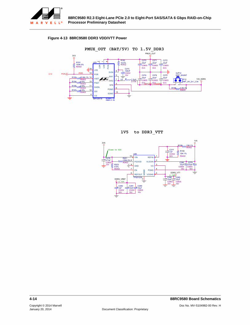
88RC9580 R2.3 Eight-Lane PCIe 2.0 to Eight-Port SAS/SATA 6 Gbps RAID-on-Chip Processor Preliminary Datasheet
4-14 88RC9580 Board Schematics
Copyright © 2014 Marvell Doc No. MV-S104982-00 Rev. HJanuary 20, 2014 Document Classification: Proprietary
Figure 4-13 88RC9580 DDR3 VDD/VTT Power
PMUX_OUT (BAT/5V) TO 1.5V_DDR3
Close to U26
0.75V
1V5 to DDR3_VTT
0.75V
88PG847_1V5DDR3
POR
PMUX_OUT
1V5_DDR3
3V3
DDR3_VREF
1V5
DDR3_VTT
2V5
POR3,12
C27910uF
C080516V
C2784.7uFC080510V
R197 0-5%R0402
NORMAL:3APEAK:4.5A
U25
88PG847B
ILIM
1LD
R2
SFB3
CG4
SW15
PGND6
SW27
PV
IN8
LFB16
PSET15
VSET14
SGND13SDI
12SHDN
11
POR10 SVIN
9
R196 0.05-1%R0805
C28010uF
C080516V
JP12DNP_UH_2x1_2.54
1 2
C2821nFC040250V
L6 1.5uH3.17A
XJP12DNP_SHUNT
R19210-5%R0402
R201100K-5%R0402
C28910uFC080516V
C273100nFC040210V
C27022uFC08056V3
U26
TPS51200
REFIN1
VLDOIN2
VO3
PGND4
VOSNS5
REFOUT6
EN7
GND8
PGOOD9
VIN10
MG
ND
11
C28110nFC040216V
R191100K-5%R0402
R198 10K-1%R0402
C27122uFC08056V3
R2030-5%R0402
R194 0-5%R0402
C27522uFC08056V3
R19910K-1%R0402
R193 53.6K-1%R0402
C27622uFC08056V3
R195 0-5%R0402
C29010uFC080516V
C2771nFC040250V
C28510uFC080516V
C27222uFC08056V3
C27422uFC08056V3
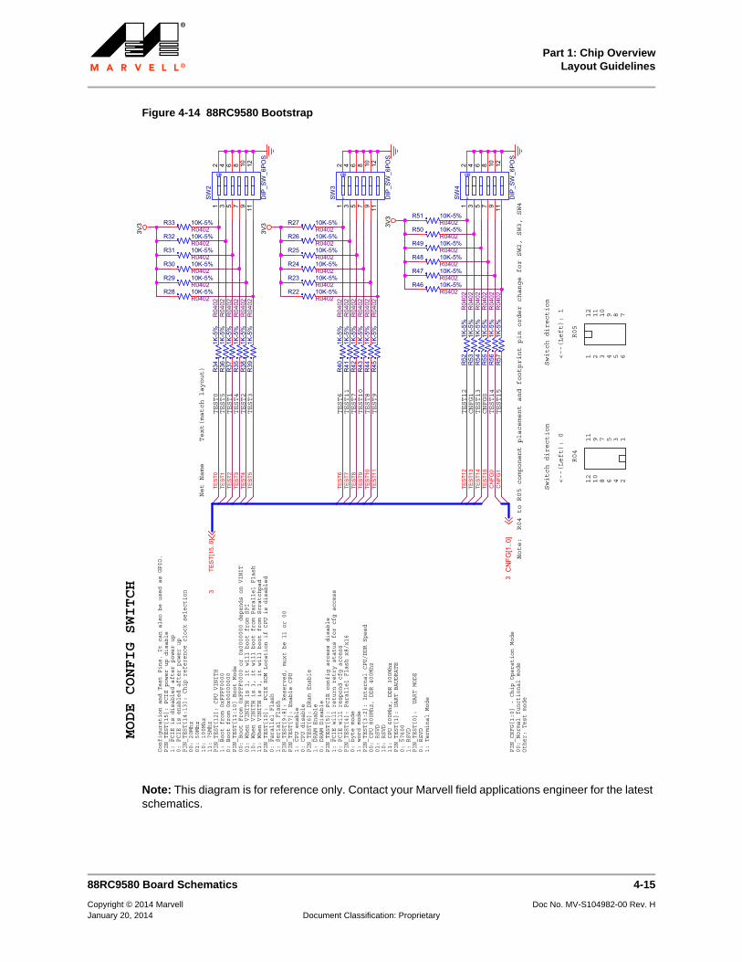
Part 1: Chip OverviewLayout Guidelines
88RC9580 Board Schematics 4-15
Copyright © 2014 Marvell Doc No. MV-S104982-00 Rev. HJanuary 20, 2014 Document Classification: Proprietary
Figure 4-14 88RC9580 Bootstrap
Note: This diagram is for reference only. Contact your Marvell field applications engineer for the latest schematics.
MODE CONFIG SWITCH
PIN_CNFG[1:0] - Chip Operation Mode
00: Normal functional mode
Other: Test mode
Configuration and Test Pins. It can also be used as GPIO.
PIN_TEST[15]: PCIE power up disable
1: PCIE is disabled after power up
0: PCIE is enabled after power up
PIN_TEST[14:13]: Chip reference clock selection
00: 20Mhz
01: 50Mhz
10: 100Mhz
11: 75Mhz
PIN_TEST[12]: CPU VINITH
1: Boot from 0xFFFF0000
0: Boot from 0x00000000
PIN_TEST[11:10] Boot Mode
00: Boot From 0xFFFF0000 or 0x0000000 depends on VINIT
01: When VINITH is 1, it will boot from SPI
10: When VINITH is 1, it will boot from Parallel Flash
11: When VINITH is 1, it will boot from Scratchpad
PIN_TEST[10]: PCIE ROM Location if CPU is disabled
0: Parallel Flash
1: Serial Flash
PIN_TEST[9:8]: Reserved, muxt be 11 or 00
PIN_TEST[7]: Enable CPU
1: CPU enable
0: CPU disable
PIN_TEST[6]: DRam Enable
1: DRAM Enable
0: DRAM Disable
PIN_TEST[5]: PCIE config access disable
1: PCIE will return retry status for cfg access
0: PCIE will respond cfg access
PIN_TEST[4]: Parallel Flash x8/x16
0: byte mode
1: word mode
PIN_TEST[3:2]: Internal CPU/DDR Speed
00: CPU 800Mhz, DDR 400Mhz
01: RSVD
10: RSVD
11: CPU 600Mhz, DDR 300Mhz
PIN_TEST[1]: UART BAUDRATE
0: 57600
1: RSVD
PIN_TEST[0]: UART MODE
0: RSVD
1: Terminal Mode
TEST0
TEST5
TEST1
TEST4
TEST2
TEST3
TEST6
TEST7
TEST8
TEST9
TEST10
TEST11
TEST12
TEST13
TEST14
TEST15
CNFG0
CNFG1
Note: R04 to R05 component placement and footprint pin order change for SW2, SW3, SW4
R04
R05
1 2 3 4 5 68 71211109
56
12
348
7
12
11
10
9
Net Name
Text(match layout)
<--(Left): 0
Switch direction
<--(Left): 1
Switch direction
TES
T7TE
ST6
TES
T10
TES
T11
TES
T8TE
ST9
TES
T12
TES
T13
TES
T5TE
ST4
TES
T3
TES
T1TE
ST2
TES
T0
TES
T14
TES
T15
CN
FG0
CN
FG1
3V3
3V3 3V
3
CN
FG[1
..0]
3
TES
T[15
..0]
3
R39
1K-5
%R
0402
R52
1K-5
%R
0402
R44
1K-5
%R
0402
R49 10K-5%R0402
1
ON
SW
3
DIP
_SW
_6P
OS
12
34
56
78
910
1112
R40
1K-5
%R
0402
R34
1K-5
%R
0402
R41
1K-5
%R
0402
R28 10K-5%R0402
R23 10K-5%R0402
R54
1K-5
%R
0402
R45
1K-5
%R
0402
R48 10K-5%R0402
R43
1K-5
%R
0402
R33 10K-5%R0402
R31 10K-5%R0402
R46 10K-5%R0402
R24 10K-5%R0402
R56
1K-5
%R
0402
R35
1K-5
%R
0402
R32 10K-5%R0402
R47 10K-5%R0402
R26 10K-5%R0402
R57
1K-5
%R
0402
R38
1K-5
%R
0402
R53
1K-5
%R
0402
1
ON
SW
2
DIP
_SW
_6P
OS
12
34
56
78
910
1112
R50 10K-5%R0402
R42
1K-5
%R
0402
R36
1K-5
%R
0402
R29 10K-5%R0402
R55
1K-5
%R
0402
R37
1K-5
%R
0402
R30 10K-5%R0402
1
ON
SW
4
DIP
_SW
_6P
OS
12
34
56
78
910
1112
R25 10K-5%R0402
R51 10K-5%R0402R27 10K-5%
R0402
R22 10K-5%R0402

88RC9580 R2.3 Eight-Lane PCIe 2.0 to Eight-Port SAS/SATA 6 Gbps RAID-on-Chip Processor Preliminary Datasheet
4-16 . Layer Stack-Up
Copyright © 2014 Marvell Doc No. MV-S104982-00 Rev. HJanuary 20, 2014 Document Classification: Proprietary
4.2 . Layer Stack-Up
The following layer stack up is recommended
Layer 1–Topside, Parts, Low and High-Speed Signal Routes, and Power Routes
Layer 2–Solid Ground Plane
Layer 3–Low and High-Speed Signals
Layer 4–Power Plane
Layer 5–Solid Ground Plane
Layer 6–Low and High Speed Signals
Layer 7–Solid Ground Plane
Layer 8–Bottom Layer, Low and High-Speed Signal Routes, and Power Routes
5 mil traces and 5 mil spacing are the recommended minimum requirements.
4.2.1 Layer 1–Topside, Parts, Low and High-Speed Signal Routes, and Power Routes
All active parts are to be placed on the topside. Some of the differential pairs for SAS/SATA and PCI Express are routed on the top layer, differential 100 ohm impedance needs to be maintained for those high-speed signals.
4.2.2 Layer 2–Solid Ground Plane
A solid ground plane should be located directly below the top layer of the PCB. This layer should be a minimum distance below the top layer in order to reduce the amount of crosstalk and EMI. There should be no cutouts in the ground plane. Use of 1 ounce copper is recommended.
4.2.3 Layer 3–Low and High-Speed Signals
Some of the high-speed signals are routed on this layer. A differential 100 ohm impedance needs to be maintained for those high speed signals.
4.2.4 Layer 4–Power Plane
Use solid planes on layer 4 to supply power to the ICs on the PCB. Avoid narrow traces and necks on this plane.
4.2.5 Layer 5–Solid Ground Plane
A solid ground plane adds balance to the board layout stack-up. It provides could coupling for the power plane on layer 4.
Part 1: Chip OverviewLayout Guidelines
. Layer Stack-Up 4-17
Copyright © 2014 Marvell Doc No. MV-S104982-00 Rev. HJanuary 20, 2014 Document Classification: Proprietary
4.2.6 Layer 6–Low and High Speed Signals
Some of the high-speed signals are routed on this layer. A differential 100 Ω impedance must be maintained for the high-speed signals.
4.2.7 Layer 7–Solid Ground Plane
A solid ground plane should be located directly below the top layer of the PCB. This layer should be a minimum distance below the top layer in order to reduce the amount of crosstalk and EMI. There should be no cutouts in the ground plane. Use of 1 ounce copper is recommended.
4.2.8 Layer 8–Bottom Layer, Low and High-Speed Signal Routes, and Power Routes
Some of the differential pairs for SAS/SATA and PCI Express are routed on the top layer. A differential 100 Ω impedance must be maintained for the high-speed signals.

88RC9580 R2.3 Eight-Lane PCIe 2.0 to Eight-Port SAS/SATA 6 Gbps RAID-on-Chip Processor Preliminary Datasheet
4-18 Power Supply
Copyright © 2014 Marvell Doc No. MV-S104982-00 Rev. HJanuary 20, 2014 Document Classification: Proprietary
4.3 Power Supply
The 88RC9580 operates using the following power supplies:
VDD Power (1.0V) for the digital core
PCI Express Analog Power Supply (1.8V)
SAS/SATA Analog Power Supply (2.5V)
General I/O Power (3.3V)
DDR I/O Power
4.3.1 VDD Power (1.0V)
All digital power pins (VDD pins) must be connected directly to a VDD plane in the power layer with short and wide traces to minimize digital power-trace inductances.
Use vias close to the VDD pins to connect to this plane and avoid using the traces on the top layer. Marvell recommends placing capacitors around the three sides of the PCB near VDD pins with the following dimensions:
0.001 µF (1 capacitor)
0.1 µF (2 capacitors)
2.2 µF (1 ceramic capacitor)
The combinations of small capacitors are used to suppress switching noise at various frequency ranges. The 2.2 µF ceramic decoupling capacitor is required to filter the lower frequency power-supply noise.
To reduce system noise, place high-frequency surface-mount monolithic ceramic bypass capacitors as close as possible to the channel VDD pins. Place at least one decoupling capacitor on each side of the IC package.
4.3.2 PCI Express Analog Power Supply (1.8V)
The analog supply provides power for the PCI Express link’s high speed serial signals. To ensure high speed link operation, use a series of bypass capacitors for the supplies. A typical capacitor value combination is 1 nF, 0.1µF, and 2.2 µF.
4.3.3 SAS/SATA Analog Power Supply (2.5V)
The analog supply provides power for the SAS/SATA link’s high speed serial signals. To ensure high speed link operation, use a series of bypass capacitors for the supplies. A typical capacitor value combination is 1 nF, 0.1µF, and 2.2 µF.
4.3.4 General I/O Power (3.3V)
A general I/O power supply provides power to the GPIO, flash and I2C blocks. A stable and clean power source is desired. Use proper bypass capacitors to provide a clean power source with good stability. A typical capacitor value combination is 0.1µF, and 2.2 µF.

Part 1: Chip OverviewLayout Guidelines
Power Supply 4-19
Copyright © 2014 Marvell Doc No. MV-S104982-00 Rev. HJanuary 20, 2014 Document Classification: Proprietary
4.3.5 DDR I/O Power
DDR I/O power provides power to the 88RC9580’s DDR I/O bank. Choose 1.5V for the DDR3 and 1.8V for DDR2. Use proper bypass capacitors to provide a clean power source with good stability. Typical capacitor values are 1 nF, 0.1µF, and 2.2 µF. The smaller capacitor is for filtering noise at higher frequencies.
4.3.6 Bias Current Resistor (RSET)
Connect a 6.04KΩ (1%) resistor between the ISET pin and the adjacent top ground plane. This resistor should lie as close as possible to the ISET pin. Avoid routing noisy signals close to the ISET pin.

88RC9580 R2.3 Eight-Lane PCIe 2.0 to Eight-Port SAS/SATA 6 Gbps RAID-on-Chip Processor Preliminary Datasheet
4-20 PCB Trace Routing
Copyright © 2014 Marvell Doc No. MV-S104982-00 Rev. HJanuary 20, 2014 Document Classification: Proprietary
4.4 PCB Trace Routing
The stack-up parameters for the reference board are shown in Table 4-1.
Table 4-1 PCB Board Stack-up Parameters
LayerLayer
DescriptionCopper Weight
(oz)Target Impedance
(±10%)
1 Signal 0.5 50
2 GND 1 N/A
3 Signal 1 50
4 Power 1 N/A
5 GND 1 N/A
6 Signal 1 50
7 GND 1 N/A
8 Signal 0.5 50

Part 1: Chip OverviewLayout Guidelines
PCB Routing Rules for DDR3-UDIMM Interface 4-21
Copyright © 2014 Marvell Doc No. MV-S104982-00 Rev. HJanuary 20, 2014 Document Classification: Proprietary
4.5 PCB Routing Rules for DDR3-UDIMM Interface
This section contains the following sections:
General Rules
Data and QS Signals
Address/Command/Control Signals
Clock Signals
4.5.1 General Rules
The following rules are ground references for all signals:
Length matching refers strictly to the total lengths of package and PCB traces. PCB traces must compensate for the length mismatch in package.
DQ byte groups are routed on the same layer.
All DDR traces must be routed as stripline only.
4.5.2 Data and QS Signals
The following rules apply to Data and QS signals:
DQ signals of the same Data byte (DQ, DM) must be length-matched to their respective DQS signals and routed within (-0.3" ± 0.05") of DQS.
The length refers to the total electrical lengths of the package and PCB. Refer to the package length provided separately.
Data signals must have trace lengths less than 4.25", and DQS traces should be less than 4.55".
Whenever possible, the DQS lines are ground guarded as GND-DQS-DQSB-GND.
If ground guarding is not possible, the spacing of DQS/ DQSB pair to other signals should be at-least 3 times the width of the trace.
The differential signals—DQS and DQSB—must be routed to a length within 0.025" (0.635mm) of each other and have a uniform fixed spacing of 1 to 1.5 times the trace width.
DQS and DQSB traces must be terminated with a resistor placed close to the processor pins.
Use 500 Ohm pull-down resistor from the DQS pin to the GND and 500 Ohm pull-up resistor from the DQSB pin to the VDDQ (controller DDR's IO power supply, not DRAM supply).
Spacing of data signals should be a minimum of 10 mils.
Data/DQM traces should have single-ended impedance of 45 Ohms to 50 Ohms.
Trace spacing from other signal groups should be greater than 3x trace width.
4.5.3 Address/Command/Control Signals
The following rules apply to Address/Command/Control signals:
The maximum trace length of address/command/control signals is 4".

88RC9580 R2.3 Eight-Lane PCIe 2.0 to Eight-Port SAS/SATA 6 Gbps RAID-on-Chip Processor Preliminary Datasheet
4-22 PCB Routing Rules for DDR3-UDIMM Interface
Copyright © 2014 Marvell Doc No. MV-S104982-00 Rev. HJanuary 20, 2014 Document Classification: Proprietary
Address/Command/Control lines must have trace impedance of 5 Ohms to 50 Ohms.
Spacing of signals should be a minimum of 10 mils.
CKE must have a pull-down resistor of 4.7-KOHms to ground.
RESET must have a pull-up resistor of 4.7-KOHms to VDDQ.
4.5.4 Clock Signals
The following rules apply to Clock signals:
Clock routing should be ground guarded for as long as possible. If ground guarding is not possible, the spacing of CLK and CLKB to other signals should be at least 3x the width of trace.
Clock signals must be length-matched to the Address/Command signals and routed longer than the Address/Command signals by (0.8" ± 0.1") to the DIMM.
Differential Clock signals—CLK and CLKB—must be routed to a length within 0.025" (0.635mm) of each other with a uniform fixed spacing of 1.5 to 2 times the trace width.
Trace spacing from other signal groups should be greater than 3x the width.
Clock signals to have a single-ended impedance of 45 Ohms to 50 Ohms. For differential impedance, there is no strict requirement, just follow the spacing rules given.

Part 1: Chip OverviewLayout Guidelines
Recommended Layout 4-23
Copyright © 2014 Marvell Doc No. MV-S104982-00 Rev. HJanuary 20, 2014 Document Classification: Proprietary
4.6 Recommended Layout
High-speed designs must consist of a good board stack-up and careful consideration of the power planes. For the 88RC9580, the following power planes are required:
VDDIO_C, VDDIO_D, and VDDIO_P power plane (3.3V power source for the digital I/O pins)
VDD (1.0V power source for the core and digital circuitry)
VAA (2.5V power source for SAS/SATA analog)
AVDD (1.8V power source for PCI Express analog)
Solid ground planes are recommended. However, special care should be taken when routing VAA, AVDD, and VSS pins.
The following general tips describe what should be considered when determining your stack-up and board routing. These tips are not meant to substitute for consulting with a signal-integrity expert or doing your own simulations.
Note: Specific numbers or rules-of-thumb are not used here because they might not be applicable in every situation.
Do not split ground planes.
Keep good spacing between possible sensitive analog circuitry on your board and the digital signals to sufficiently isolate noise. A solid ground plane is necessary to provide a good return path for routing layers. Try to provide at least one ground plane adjacent to all routing layers (see Figure 4-15).
Keep trace layers as close as possible to the adjacent ground or power planes.
This helps minimize crosstalk and improve noise control on the planes.
Figure 4-15 Trace Has At Least One Solid Plane For Return Path
When routing adjacent to only a power plane, do not cross splits.
Route traces only over the power plane that supplies both the driver and the load. Otherwise, provide a decoupling capacitor near the trace at the end that is not supplied by the adjacent power plane.
Critical signals should avoid running parallel and close to or directly over a gap.
This would change the impedance of the trace.
Separate analog powers onto opposing planes.
This helps minimize the coupling area that an analog plane has with an adjacent digital plane.
GND
V2
V1

88RC9580 R2.3 Eight-Lane PCIe 2.0 to Eight-Port SAS/SATA 6 Gbps RAID-on-Chip Processor Preliminary Datasheet
4-24 Recommended Layout
Copyright © 2014 Marvell Doc No. MV-S104982-00 Rev. HJanuary 20, 2014 Document Classification: Proprietary
For dual strip-line routing, traces should only cross at 90 degrees.
Avoid more than two routing layers in a row to minimize tandem crosstalk and to better control impedance.
Planes should be evenly distributed in order to minimize warping.
Calculating or modeling impedance should be made prior to routing.
This helps ensure that a reasonable trace thickness is used and that the desired board thickness is available. Consult with your board fabricator for accurate impedance.
Allow good separation between fast signals to avoid crosstalk.
Crosstalk increases as the parallel traces get longer.
When packages become smaller, route traces over a split power plane
Smaller packages force vias to become smaller, thereby reducing board thickness and layer counts, which might create the need to route traces over a split power plane. Some alternatives to provide return path for these signals are listed below.
Caution must be used when applying these techniques. Digital traces should not cross over analog planes, and vice-versa. All of these rules must be followed closely to prevent noise contamination problems that might arise due to routing over the wrong plane.
By tightly controlling the return path, control noise on the power and ground planes can be controlled.
Place a ground layer close enough to the split power plane in order to couple enough to provide buried capacitance, such as SIG-PWR-GND (see Figure 4-16). Return signals that encounter splits in this situation simply jumps to the ground plane, over the split, and back to the other power plane. Buried capacitance provides the benefit of adding low inductance decoupling to your board. Your fabricator may charge for a special license fee and special materials. To determine the amount of capacitance your planes provide, use the following equation:
Where ER is the dielectric coefficient, L • W represents the area of copper, and H is the separation between planes.
Provide return-path capacitors that connect to both power planes and jumps the split. Place them close to the traces so that there is one capacitor for every four or five traces. The capacitors would then provide the return path (see Figure 4-17).
Allow only static or slow signals on layers where they are adjacent to split planes.
Figure 4-16 shows the ground layer close to the split power plane.
Figure 4-16 Close Power and Ground Planes Provide Coupling For Good Return Path
C 1.249 10 13–• Er• L• W H⁄•=
V2 PLANE
GND PLANE
V1 PLANEH

Part 1: Chip OverviewLayout Guidelines
Recommended Layout 4-25
Copyright © 2014 Marvell Doc No. MV-S104982-00 Rev. HJanuary 20, 2014 Document Classification: Proprietary
Figure 4-17 shows the thermal ground plane in relation to the return-path capacitor.
Figure 4-17 Suggested Thermal Ground Plane On Opposite Side of Chip
V1
V2
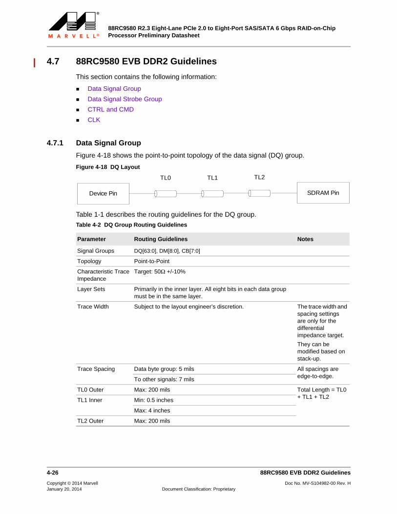
88RC9580 R2.3 Eight-Lane PCIe 2.0 to Eight-Port SAS/SATA 6 Gbps RAID-on-Chip Processor Preliminary Datasheet
4-26 88RC9580 EVB DDR2 Guidelines
Copyright © 2014 Marvell Doc No. MV-S104982-00 Rev. HJanuary 20, 2014 Document Classification: Proprietary
4.7 88RC9580 EVB DDR2 Guidelines
This section contains the following information:
Data Signal Group
Data Signal Strobe Group
CTRL and CMD
CLK
4.7.1 Data Signal Group
Figure 4-18 shows the point-to-point topology of the data signal (DQ) group.
Figure 4-18 DQ Layout
Table 1-1 describes the routing guidelines for the DQ group.
Table 4-2 DQ Group Routing Guidelines
Parameter Routing Guidelines Notes
Signal Groups DQ[63:0], DM[8:0], CB[7:0]
Topology Point-to-Point
Characteristic Trace Impedance
Target: 50Ω +/-10%
Layer Sets Primarily in the inner layer. All eight bits in each data group must be in the same layer.
Trace Width Subject to the layout engineer’s discretion. The trace width and spacing settings are only for the differential impedance target.
They can be modified based on stack-up.
Trace Spacing Data byte group: 5 mils All spacings are edge-to-edge.To other signals: 7 mils
TL0 Outer Max: 200 mils Total Length = TL0 + TL1 + TL2TL1 Inner Min: 0.5 inches
Max: 4 inches
TL2 Outer Max: 200 mils
Device Pin SDRAM Pin
TL0 TL1 TL2

Part 1: Chip OverviewLayout Guidelines
88RC9580 EVB DDR2 Guidelines 4-27
Copyright © 2014 Marvell Doc No. MV-S104982-00 Rev. HJanuary 20, 2014 Document Classification: Proprietary
4.7.2 Data Signal Strobe Group
Figure 4-19 shows the point-to-point topology of the Data Signal Strobe (DQS) signal layout.
Figure 4-19 DQS Layout
Table 4-3 describes the routing guidelines for the DQ layout.
Length Matching Requirements
Length mismatch is the difference between total length.
Number of Vias per signal
Max: Four The via count must be the same for all bits in a given byte group.
Table 4-3 DQS Layout Routing Guidelines
Parameter Routing Guidelines Notes
Signal Groups DQS[8:0], DQSB[8:0]
Topology Point-to-Point DQS has a 499Ω 1% pull down
DQS# has a 499Ω 1% pull up to 1.5 volts. Resistors are placed near the controller.
Characteristic Trace Impedance (Zo)
Single-End Target: 50Ω +/-10%
Table 4-2 DQ Group Routing Guidelines (continued)
Parameter Routing Guidelines Notes
Signal Length Mismatch Relative To
DQ[7:0], DM0 +/- 25 mils DQS0
DQ[15:8], DM1 +/- 25 mils DQS1
DQ[23:16], DM2 +/- 25 mils DQS2
DQ[31:24], DM3 +/- 25 mils DQS3
DQ[39:32], DM4 +/- 25 mils DQS4
DQ[47:40], DM5 +/- 25 mils DQS5
DQ[55:48], DM6 +/- 25 mils DQS6
DQ[63:56], DM7 +/- 25 mils DQS7
CB[7:0], DM8 +/- 25 mils CBS
Device Pin SDRAM Pin
TL0 TL1 TL2

88RC9580 R2.3 Eight-Lane PCIe 2.0 to Eight-Port SAS/SATA 6 Gbps RAID-on-Chip Processor Preliminary Datasheet
4-28 88RC9580 EVB DDR2 Guidelines
Copyright © 2014 Marvell Doc No. MV-S104982-00 Rev. HJanuary 20, 2014 Document Classification: Proprietary
Layer Sets Mainly in inner layer. The length on the outer layer should be limited to 200 mils.
Trace Width Same as DQ. The trace width and spacing settings are only for the differential impedance target.
They can be modified based on stack-up.
Trace Spacing In diff pairs: 1x to 2x trace width The trace width and spacing settings are only for the differential impedance target.
They can be modified based on stack-up.
To other signals = 10 mils
TL0 Outer Max: 200 mils Total Length = TL0 + TL1 + TL2TL1 Inner Min: 0.5 inches
Max: 4 inches
TL2 Outer Max: 200 mils
Length Matching Requirements
• Length mismatch means the difference between total length.
• CK/CK# Length = X, DQS Length = Y, where ( X - 0.25" ) ? Y ? ( X + 0.25" ).
• The phase difference within diff pair should be kept in 10 mils.
Number of vias per signal
Max: Four The via count must be the same for all bits in a given byte group.
Table 4-3 DQS Layout Routing Guidelines (continued)
Parameter Routing Guidelines Notes
Signal Length Mismatch Relative To
DQ[7:0], CBS +/- 250 mils CK0
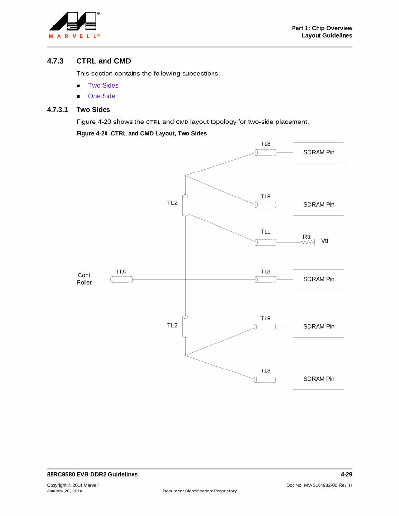
Part 1: Chip OverviewLayout Guidelines
88RC9580 EVB DDR2 Guidelines 4-29
Copyright © 2014 Marvell Doc No. MV-S104982-00 Rev. HJanuary 20, 2014 Document Classification: Proprietary
4.7.3 CTRL and CMD
This section contains the following subsections:
Two Sides
One Side
4.7.3.1 Two Sides
Figure 4-20 shows the CTRL and CMD layout topology for two-side placement.
Figure 4-20 CTRL and CMD Layout, Two Sides
SDRAM Pin
SDRAM Pin
SDRAM Pin
SDRAM Pin
SDRAM Pin
TL2
TL2
TL8
TL8
TL1
TL8
TL8
TL8
RttVtt
TL0Cont Roller

88RC9580 R2.3 Eight-Lane PCIe 2.0 to Eight-Port SAS/SATA 6 Gbps RAID-on-Chip Processor Preliminary Datasheet
4-30 88RC9580 EVB DDR2 Guidelines
Copyright © 2014 Marvell Doc No. MV-S104982-00 Rev. HJanuary 20, 2014 Document Classification: Proprietary
Table 1-3 describes the routing guidelines for the two-sided CTRL and CMD layout.
Table 4-4 CTRL and CMD Layout Routing Guidelines—Two-Side Placement
Parameter Routing Guidelines Notes
Signal Group CTRL and CMD—A[13:0], BA[2:0], CAS, RAS, WE, CKE, CS, ODT
Topology Shown in Figure 4-20. For placement on both sides only.
Characteristic Trace Impedance (Zo)
Target: 50Ω +/-10%
Layer Sets Microstrip or stripline.
Trace Spacing In group: 5 mils
To other signals = 7 mils
TL0 Max: 3000 mils
TL1 Max: 500 mils
TL2 Max: 1000 mils Each TL2 in a signal should be kept within a skew of 50 mils
TL8 Max: 200 mils
Length Matching Requirements
Longest Length = max (TL0 + TL2 + TL8)
Termination resistor 50Ω +/− 10%
Number of vias per signal
No concern.
Signal Length Mismatch Relative To
A[13:0], BA[2:0], CAS, RAS, WE, CKE, CS, ODT
+600; +/- 300 mils CK0

Part 1: Chip OverviewLayout Guidelines
88RC9580 EVB DDR2 Guidelines 4-31
Copyright © 2014 Marvell Doc No. MV-S104982-00 Rev. HJanuary 20, 2014 Document Classification: Proprietary
4.7.3.2 One Side
Figure 4-21 shows the topology of the CTRL and CMD layout for single-side placement.
Figure 4-21 CTRL and CMD Layout—Single-Side Placement
Table 4-5 describes the routing guidelines for the single-sided CTRL and CMD layout. for single-side placement.
Table 4-5 CTRL and CMD Layout Routing Guidelines, Single-Sided Placement
Parameter Routing Guidelines Notes
Signal Group CTRL and CMD—A[13:0], BA[2:0], CAS, RAS, WE, CKE, CS, ODT
Topology Shown in Figure 4-21. For single-side placement only.
Characteristic Trace Impedance (Zo)
Target: 50Ω +/-10%
Layer Sets Microstrip or stripline
SDRAM Pin
SDRAM Pin
SDRAM Pin
SDRAM Pin
SDRAM Pin
TL2
TL3
TL7
TL7
TL1
TL8
TL8
RttVtt
TL0Cont Roller

88RC9580 R2.3 Eight-Lane PCIe 2.0 to Eight-Port SAS/SATA 6 Gbps RAID-on-Chip Processor Preliminary Datasheet
4-32 88RC9580 EVB DDR2 Guidelines
Copyright © 2014 Marvell Doc No. MV-S104982-00 Rev. HJanuary 20, 2014 Document Classification: Proprietary
4.7.4 CLK
Table 4-5 describes the routing guidelines for the single-sided CTRL and CMD layout. for single-sided placement.
Trace Spacing In group: 5 mils
To other signals = 7 mils
TL0 Max: 3000 mils
TL1 Max: 500 mils
TL2 Max: 1200 mils The skew between TL2 and TL3 should be limited to 50 mils.
TL3 Max: 1200 mils
TL7 Max: 500 mils Each TL7/8 in a signal should be kept within a skew of 50 mils.
TL8 Max: 700 mils
Length Matching Requirements
Longest Length = max (TL0 + TL2 + TL8)
Termination resistor 50Ω +/− 10%
Number of vias per signal
No concern.
Table 4-6 CTRL and CMD Layout Routing Guidelines, Single-Sided Placement
Parameter Routing Guidelines Notes
Signal Group CLK to CK[2:0], CK#[2:0]
Topology Far-end cluster For single-side placement only.
Characteristic Trace Impedance (Zo)
Single-end target: 50Ω +/-10%
Layer Sets Mainly in inner layer, the length on the outer layer should be limited in 200 mils.
Trace Width Same as Addr/CMD, based on the stackup.
Trace Spacing In diff pair: 1x to 2x trace width
To other signals = 12 mils
Table 4-5 CTRL and CMD Layout Routing Guidelines, Single-Sided Placement (continued)
Parameter Routing Guidelines Notes
Signal Length Mismatch Relative To
A[13:0], BA[2:0], CAS, RAS, WE, CKE, CS, ODT
+600; +/- 300 mils CK

Part 1: Chip OverviewLayout Guidelines
88RC9580 EVB DDR2 Guidelines 4-33
Copyright © 2014 Marvell Doc No. MV-S104982-00 Rev. HJanuary 20, 2014 Document Classification: Proprietary
Length Matching Requirements
The length of CK0 and CK1 signals for four chips should be controlled within a skew of 30 mils. Here, CK2 drives only one SDRAM.
Termination resistor 100Ω +/− 10%
Number of vias per signal
No Concern. The via count must be the same for all bits in a given byte group.
Table 4-6 CTRL and CMD Layout Routing Guidelines, Single-Sided Placement (continued)
Parameter Routing Guidelines Notes
Signal Length Mismatch Relative To
CK2 +120; +/- 15 mils CK0
CK1 +/- 15 mils CK0
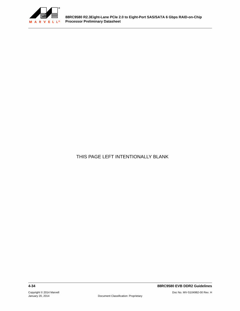
THIS PAGE LEFT INTENTIONALLY BLANK
88RC9580 R2.3Eight-Lane PCIe 2.0 to Eight-Port SAS/SATA 6 Gbps RAID-on-Chip Processor Preliminary Datasheet
4-34 88RC9580 EVB DDR2 Guidelines
Copyright © 2014 Marvell Doc No. MV-S104982-00 Rev. HJanuary 20, 2014 Document Classification: Proprietary

Part 1: Chip OverviewElectrical Specifications
5-1
Copyright © 2014 Marvell Doc No. MV-S104982-00 Rev. HJanuary 20, 2014 Document Classification: Proprietary
5 ELECTRICAL SPECIFICATIONS
This chapter contains the following sections:
Absolute Maximum Ratings
Recommended Operating Conditions
DC Electrical Characteristics
Thermal Data
AC Timing

88RC9580 R2.3 Eight-Lane PCIe 2.0 to Eight-Port SAS/SATA 6 Gbps RAID-on-Chip Processor Preliminary Datasheet
5-2 Absolute Maximum Ratings
Copyright © 2014 Marvell Doc No. MV-S104982-00 Rev. HJanuary 20, 2014 Document Classification: Proprietary
5.1 Absolute Maximum Ratings
CAUTION: Exposure to conditions at or beyond the maximum rating may damage the device. Operation beyond the recommended operating conditions (Table 5-2) is neither recommended nor guaranteed.
Note: Before designing a system, it is recommended that you read application note AN-63: Thermal Management for Marvell Technology Products. This application note presents basic concepts of thermal management for integrated circuits (ICs) and includes guidelines to ensure optimal operating conditions for Marvell Technology's products.
Table 5-1 Absolute Maximum Ratings
Parameter Symbol Min Typ Max Units
Absolute Analog Power for PCIe PHY AVDD[8:0] 1.62 1.8 1.98 V
Absolute Analog Power for SAS/SATA PHY, Chip PLL
VAA[7:0], VAA_ANA, VAA_PLL, AVDD25_0, AVDD25_1
2.25 2.5 2.75 V
Absolute Power for DDR I/O, DDR DLL
DDR2
DDR3
VDDQ, AVDD_DDR 1.6
1.35
1.8
1.5
2.0
1.65
V
V
Absolute Power for Digital Core VDD, VHV 0.9 1.0 1.1 V
Absolute Digital I/O Power VDDO1 3 3.3 3.6 V

Part 1: Chip OverviewElectrical Specifications
Recommended Operating Conditions 5-3
Copyright © 2014 Marvell Doc No. MV-S104982-00 Rev. HJanuary 20, 2014 Document Classification: Proprietary
5.2 Recommended Operating Conditions
CAUTION: Operation beyond the recommended operating conditions is neither recommended nor guaranteed.
Table 5-2 Recommended Operating Conditions
Parameter Symbol Min Typ Max Units
Analog Power for PCIe PHY AVDD[8:0] 1.71 1.8 1.89 V
Analog Power for SAS/SATA PHY, Chip PLL
VAA[7:0], VAA_ANA
2.38 2.5 2.63 V
Digital Power for DDR I/O, DDR DLL
DDR2
DDR3
VDDQ, AVDD_DDR 1.71
1.42
1.8
1.5
1.89
1.58
V
V
Digital Core Power VDD 0.95 1.0 1.05 V
Digital I/O Power VDDO1 3.14 3.3 3.47 V
PCIe Internal Bias Reference PIN_ISET 4.75 5.0 5.25 KΩ
SAS/SATA PHY Internal Bias Reference
ISET 5.74 6.04 6.34 KΩ
Ambient Operating Temperature TA 0 70 °C
Junction Operating Temperature TJ 0 125 °C

88RC9580 R2.3 Eight-Lane PCIe 2.0 to Eight-Port SAS/SATA 6 Gbps RAID-on-Chip Processor Preliminary Datasheet
5-4 DC Electrical Characteristics
Copyright © 2014 Marvell Doc No. MV-S104982-00 Rev. HJanuary 20, 2014 Document Classification: Proprietary
5.3 DC Electrical Characteristics
CAUTION: Operation beyond the recommended operating conditions is neither recommended nor guaranteed.
Table 5-3 DC Electrical Characteristics
Parameter Symbol Min Typ Max Units
Analog Power for PCIe PHY 1.8V IAVDD 0.80 A
Analog Power for SAS/SATA PHY 2.5V, Chip PLL IVAA 0.80 A
Digital Power for DDR I/O, DDR DLL
DDR2
DDR3
1.0
1.0
A
A
Digital Core Power IVDD 3.5 A
Digital I/O Power IVDDO 100 mA
Input Low Voltage of Digital I/O VIL -0.4 0.8 V
Input High Voltage of Digital I/O VIH 2.0 3.6 V
Output Low Voltage of Digital I/O VOL 0.13 V
Output High Voltage of Digital I/O VOH 2.0 VDDO1 V

Part 1: Chip OverviewElectrical Specifications
Thermal Data 5-5
Copyright © 2014 Marvell Doc No. MV-S104982-00 Rev. HJanuary 20, 2014 Document Classification: Proprietary
5.4 Thermal Data
It is recommended to read application note AN-63 Thermal Management for Selected Marvell® Products (Document Number MV-S300281-00) and the ThetaJC, ThetaJA, and Temperature Calculations White Paper, available from Marvell, before designing a system. These documents describe the basic understanding of thermal management of integrated circuits (ICs) and guidelines to ensure optimal operating conditions for Marvell products.
Table 5-4 provides the thermal data for the 88RC9580. The simulation was performed according to JEDEC standards.
Table 5-4 shows the values for the package thermal parameters for the 676-pin FCBGA mounted on a 4-layer PCB.
Table 5-4 Package Thermal Data, 4-Layer PCB*
* All data is based on parts mounted on a 101.5 mm x 114.5 mm x 1.6 mm JEDEC 4L PCB.
Parameter DefinitionAirflow Value
0 m/s 1 m/s 2 m/s 3 m/s
θJA Thermal resistance: junction to ambient (no heat sink)
10.94 C/W 9.46 C/W 8.82 C/W 8.42 C/W
ψJT Thermal characterization parameter: junction to top center (no heat sink)
0.23 C/W 0.23 C/W 0.23 C/W 0.23 C/W
θJA Thermal resistance: junction to ambient (with heat sink)
4.76 C/W 2.28 C/W 2.00 C/W 1.90 C/W
ψJT Thermal characterization parameter: junction to top center (with heat sink)
0.34 C/W 0.36 C/W 0.36 C/W 0.36 C/W
θJC Thermal resistance: junction to case
0.39 C/W – – –

88RC9580 R2.3 Eight-Lane PCIe 2.0 to Eight-Port SAS/SATA 6 Gbps RAID-on-Chip Processor Preliminary Datasheet
5-6 AC Timing
Copyright © 2014 Marvell Doc No. MV-S104982-00 Rev. HJanuary 20, 2014 Document Classification: Proprietary
5.5 AC Timing
This section discusses the following topics:
SATA
PCIe
DDR3
Parallel Flash and NVSRAM
5.5.1 SATA
This product conforms to AC timing requirements as specified in the Serial ATA Revision 3.0 Specification (www.sata-io.org).
5.5.2 PCIe
This product conforms to AC timing requirements as specified in the PCI Express® Base 2.0 specification (www.pcisig.com/).
5.5.3 DDR3
This section provides the timing diagrams and parameters for the Dynamic Memory Controller on the External Memory Pin Interface.
5.5.3.1 Timing Diagrams
This section contains the following figures:
Figure 5-1, DDR3 SDRAM Timing
Figure 5-2, MD[31:0] to DQS Write Skew
Figure 5-3, CLK to Address/Command Write Skew
Figure 5-4, DQS to CLK Write Skew
Figure 5-5, MD[31:0] to DQS Read Skew
Figure 5-6, Reference Load

Part 1: Chip OverviewElectrical Specifications
AC Timing 5-7
Copyright © 2014 Marvell Doc No. MV-S104982-00 Rev. HJanuary 20, 2014 Document Classification: Proprietary
Figure 5-1 DDR3 SDRAM Timing
Note: From JEDEC Standard: DDR3 SDRAM Specification
Note: BL8, WL = 5 (AL = 0, CWL = 5)
Note: DIN n = data-in from column n.
Note: NOP commands are shown for ease of illustration; other commands may be valid at these times.
Note: BL8 setting is activated by either MR0[A1:0 = 00] or MR0[A1:0 = 01] and A12 = 1 during WRITE command at T0.
Note: tDQSS must be met at each rising clock edge.
DIN
n + 3DIN
n + 2DIN
n + 1DIN
n
WL = AL + CWL
T0 T1 T2 T3 T4 T5 T6 T7 T8 T9 T10
DIN
n + 7DIN
n + 6DIN
n + 5DIN
n + 4
Bank,Col n
NOPWRITE NOPNOP NOP NOP NOP NOP NOP NOP NOP
CK
CK#
COMMAND3
DQ2
DQS, DQS#
ADDRESS4
tWPST(min)
tWPST(min)
tDQSL
tDQSS(min)
DIN
n + 3DIN
n + 2DIN
n + 1DIN
nDIN
n + 7DIN
n + 6DIN
n + 5DIN
n + 4DQ2
DIN
n + 3DIN
n + 2DIN
n + 1DIN
nDIN
n + 7DIN
n + 6DIN
n + 5DIN
n + 4DQ2
DQS, DQS#
DQS, DQS#
tDQSS(max)
tDQSS(nominal)
tDQSL
tWPRE(min)
tDQSL
tDQSS
tDQSS
tDSS tDSS tDSS tDSS tDSS
tDSH tDSH tDSH tDSH
tDSS tDSS tDSS tDSS tDSS
tDSS tDSS tDSS tDSS tDSS
tDSH tDSH tDSH tDSH
tDSH tDSH tDSH tDSH
tDQSLtDQSH tDQSLtDQSH tDQSLtDQSH tDQSH
tDQSLtDQSH tDQSLtDQSH tDQSLtDQSH tDQSH
tDQSLtDQSH tDQSLtDQSH tDQSLtDQSH tDQSH
tWPRE(min)
tWPRE(min)
tDQSH(min)
tDQSH(min)
tDQSH(min)
tWPST(min)
tDQSL(min)
tDQSL(min)
tDQSL(min)
DM
DM
DM

88RC9580 R2.3 Eight-Lane PCIe 2.0 to Eight-Port SAS/SATA 6 Gbps RAID-on-Chip Processor Preliminary Datasheet
5-8 AC Timing
Copyright © 2014 Marvell Doc No. MV-S104982-00 Rev. HJanuary 20, 2014 Document Classification: Proprietary
Figure 5-2 MD[31:0] to DQS Write Skew
Figure 5-3 CLK to Address/Command Write Skew
Figure 5-4 DQS to CLK Write Skew
tDQTVB tDQTVA tDQTVB tDQTVA
1000 ps 2000 ps 3000 ps0 ps
DQS
DQS
DQS
CLK
CLK
ADDR / CMD / CNTRL
tATVR tATVA
1000 ps 2000 ps 3000 ps0 ps
CLK#
CLK
CLK
CLK
1000 ps 2000 ps 3000 ps0 ps
CLK#
CLK
DQS DQS
DQS#
tDQSSmch
DQS

Part 1: Chip OverviewElectrical Specifications
AC Timing 5-9
Copyright © 2014 Marvell Doc No. MV-S104982-00 Rev. HJanuary 20, 2014 Document Classification: Proprietary
Figure 5-5 MD[31:0] to DQS Read Skew
Table 5-5 DDR Timing Specifications for 400 MHz
Symbol Description Min Typ Max Units Notes
tCK Clock Low Level Width - 2.5 - nS -
tCL Clock Low Level Width 0.48 0.52 tCK (avg) -
tCH Clock High Level Width 0.48 0.52 tCK (avg) -
tCK (JITTER) CLK Jitter at Output Pin (c-c) -100 100 ps -
tCK_DC Duty Cycle as Output Pin 48 52 tCK -
tDQTVB DQ Valid Time Before DQS 0.4 - - ns Timing specified to reference load (25 Ohms to VTT)
tDQTVA DQ Valid Time After DQS 0.42 - - ns Timing specified to reference load (25 Ohms to VTT)
tATVB CMD/CTL Valid Time Before CK 0.9 - - ns Timing specified to reference load (25 Ohms to VTT)
tATVA CMD/CTL Valid Time After CK 0.94 - - ns Timing specified to reference load (25 Ohms to VTT)
tDQSSMC Skew Between CK and DQS -0.1 - 0.1 tCK (avg) Timing specified to reference load (25 Ohms to VTT)
tSUMC Maximum Setup Skew Allowed between DQ and DQS During Read from DQS Transition
- - 0.41 ns The setup and hold timing is for reference slew rate of 1 V/ns for QDQ and 2V/ns for DQS (diff). refer to derating table for other slew rates.
tHDMC Hold Factor for Valid DQ WRT DWS Rising/Falling Edge During Read
0.84 - - ns The setup and hold timing is for reference slew rate of 1 V/ns for QDQ and 2V/ns for DQS (diff). refer to derating table for other slew rates.
tWPREMC DQS, DQS# Differential Write Preamble 1 - - tCK (avg)
tWPSTMC DQS, DQS# Differential Write Postamble 0.45 - - tCK (avg)
1000 ps 2000 ps 3000 ps0 ps
DQS
DQS
tSUmch
tHDmch
tSUmch
tHDmch

88RC9580 R2.3 Eight-Lane PCIe 2.0 to Eight-Port SAS/SATA 6 Gbps RAID-on-Chip Processor Preliminary Datasheet
5-10 AC Timing
Copyright © 2014 Marvell Doc No. MV-S104982-00 Rev. HJanuary 20, 2014 Document Classification: Proprietary
5.5.3.2 Reference Load
Figure 5-6 shows the reference load for AC timing.
Figure 5-6 Reference Load
5.5.3.3 Derating Tables
Figure 5-6 describes Setup Derating.
Figure 5-7 describes Hold Derating.
tIPWMC Control and Address Input Pulse Width 0.7 - - tCK (avg)
tDIPWMC DQ and DM Input Pulse Width 0.35 - - tCK (avg)
Table 5-6 Setup Derating
DQS Slew
DQ Slew (V/ns) 1 2 4 6 8 10
0.5 0 60 107 136 149 159
2 -36 0 43 72 85 94
3 -65 -32 0 22 35 45
3 -79 -45 -18 0 21 30
4 -87 -54 -27 -5 0 18
5 -93 -59 -32 -14 -1 0
Table 5-7 Hold Derating
DQS Slew
DQ Slew (V/ns) 1 2 4 6 8 10
0.5 0 -36 -65 -79 -89 -93
2 60 0 -32 -45 -54 -59
3 107 43 0 -18 -27 -32
3 136 72 22 0 -5 -14
4 149 85 35 21 0 -1
5 159 94 45 30 18 0
Table 5-5 DDR Timing Specifications for 400 MHz (continued)
Symbol Description Min Typ Max Units Notes
DUT
DQDQSDQS
RDQSRDQS
Output
Timing Reference Point
25Ω
VTT = VDDQ/2

Part 1: Chip OverviewElectrical Specifications
AC Timing 5-11
Copyright © 2014 Marvell Doc No. MV-S104982-00 Rev. HJanuary 20, 2014 Document Classification: Proprietary
5.5.4 Parallel Flash and NVSRAM
This section describes the timing for Parallel Flash and NVSRAM.
Figure 5-7 illustrates the Parallel Flash and NVSRAM Read timing, and Table 5-8 provides parameter information for the timing diagram.
Figure 5-7 Parallel Flash / NVSRAM Read Timing.
Table 5-8 Timing Parameters for Figure 5-7, Parallel Flash / NVSRAM Read Timing.
Parameter Description NVSRAM Parallel Flash Unit
tRC Read Cycle Time (NV_RD_CYCLE_TM (R0C968h [7:0]) + 2) * Tclk
(FLSH_RD_CYCLE_TM (R0C978h [7:0]) + 2) * Tclk
ns
tRCEL Read CE Assert Time (NV_RD_CE_ASSRT_TM (R0C96Ch [23:16]) + 1) * Tclk
(FLSH_RD_CE_ASSRT_TM (R0C97Ch [23:16]) + 1) * Tclk
ns
tRCEH Read CE Deassert Time (NV_RD_CE_DEASSRT_TM (R0C96Ch [31:24]) + 2) * Tclk
(FLSH_RD_CE_DEASSRT_TM (R0C97Ch [31:24]) + 2) * Tclk
ns
tOEL Read OE Assert Time (NV_RD_OE_ASSRT_TM (R0C96Ch [7:0]) + 1) * Tclk
(FLSH_RD_OE_ASSRT_TM (R0C97Ch [7:0]) + 1) * Tclk
ns
tOEH Read OE Deassert Time (NV_RD_OE_DEASSRT_TM (R0C96Ch [15:8]) + 2) * Tclk
(FLSH_RD_OE_DEASSRT_TM (R0C97Ch [15:8]) + 2) * Tclk
ns
tACC Read Data Latch Time (NV_RD_DATA_LTCH_TM (R0C968h [15:8]) + 1) * Tclk - 20
(FLSH_RD_DATA_LTCH_TM (R0C978h [15:8]) + 1) * Tclk - 20
ns
Address Valid
Input Data Valid
tRC
tRCEH
tRCEL
tOEL
tACC
tOEH
P_ADDR
CE_N
OE_N
P_DATA

88RC9580 R2.3 Eight-Lane PCIe 2.0 to Eight-Port SAS/SATA 6 Gbps RAID-on-Chip Processor Preliminary Datasheet
5-12 AC Timing
Copyright © 2014 Marvell Doc No. MV-S104982-00 Rev. HJanuary 20, 2014 Document Classification: Proprietary
Figure 5-8 illustrates the Parallel Flash and NVSRAM Write timing, and Table 5-9 provides parameter information for the timing diagram.
Figure 5-8 Parallel Flash / NVSRAM Write Timing
Table 5-9 Timing Parameters for Figure 5-7, Parallel Flash / NVSRAM Read Timing.
Parameter Description NVSRAM Parallel Flash Unit
tWC Write Cycle Time (NV_WRT_CYCLE_TM (R0C960h [7:0]) + 2) * Tclk
(FLSH_WRT_CYCLE_TM (R0C970h [7:0]) + 2) * Tclk
ns
tWCEL Write CE Assert Time (NV_CE_ASSRT_TM (R0C960h [15:8]) + 1) * Tclk
(FLSH_CE_ASSRT_TM (R0C970h [15:8]) + 1) * Tclk
ns
tWCEH Write CE Deassert Time (NV_CE_DEASSRT_TM (R0C960h [23:16]) + 2) * Tclk
(FLSH_CE_DEASSRT_TM (R0C970h [23:16]) + 2) * Tclk
ns
tWEL Write WE Assert Time (NV_WRT_WE_ASSRT_TM (R0C964h [7:0]) + 1) * Tclk
(FLSH_WRT_WE_ASSRT_TM (R0C974h [7:0]) + 1) * Tclk
ns
tWEH Read WE Deassert Time (NV_WRT_WE_DEASSRT_TM (R0C964h [15:8]) + 2) * Tclk
(FLSH_WRT_WE_DEASSRT_TM (R0C974h [15:8]) + 2) * Tclk
ns
tDL Write Data IO Enable Time
(NV_WRT_DATA_IO_EN_TM (R0C964h [23:16]) + 1) * Tclk
(FLSH_WRT_DATA_IO_EN_TM (R0C974h [23:16]) + 1) * Tclk
ns
tDH Write Data IO Disable Time
(NV_WRT_DATA_IO_DSBL_TM (R0C964h [31:24]) + 2) * Tclk
(FLSH_WRT_DATA_IO_DSBL_TM (R0C974h [31:24]) + 2) * Tclk
ns
Address Valid
tWC
tWCEH
tWCEL
tWEL
tDH
tWEH
Output Data ValidtDL
P_ADDR
CE_N
WE_N
P_DATA


Marvell Semiconductor, Inc.5488 Marvell Lane
Santa Clara, CA 95054, USA
Tel: 1.408.222.2500Fax: 1.408.752.9028
www.marvell.com
Marvell. Moving Forward Faster