marvell - storage - 88se948x datasheet...marvell. marvell retains the right to make changes to this...
TRANSCRIPT

Doc No. MV-S105606-00 Rev. J
April 23, 2015
Document Classification: ProprietaryMarvell. Moving Forward Faster
88SE9480/88SE9485 R3.3Eight-Lane PCI-Express 2.0 to Eight-Port SAS/SATA 6 Gbps RAID I/O Controller
Preliminary Datasheet

88SE9480/88SE9485 R3.3 Eight-Lane PCI-Express 2.0 to Eight-Port SAS/SATA 6 Gbps RAID I/O Controller
No part of this document may be reproduced or transmitted in any form or by any means, electronic or mechanical, including photocopying and recording, for any purpose, without the express written permission of Marvell. Marvell retains the right to make changes to this document at any time, without notice. Marvell makes no warranty of any kind, expressed or implied, with regard to any information contained in this document, including, but not limited to, the implied warranties of merchantability or fitness for any particular purpose. Further, Marvell does not warrant the accuracy or completeness of the information, text, graphics, or other items contained within this document. Marvell products are not designed for use in life-support equipment or applications that would cause a life-threatening situation if any such products failed. Do not use Marvell products in these types of equipment or applications. With respect to the products described herein, the user or recipient, in the absence of appropriate U.S. government authorization, agrees: 1) Not to re-export or release any such information consisting of technology, software or source code controlled for national security reasons by the U.S. Export Control Regulations ("EAR"), to a national of EAR Country Groups D:1 or E:2; 2) Not to export the direct product of such technology or such software, to EAR Country Groups D:1 or E:2, if such technology or software and direct products thereof are controlled for national security reasons by the EAR; and, 3) In the case of technology controlled for national security reasons under the EAR where the direct product of the technology is a complete plant or component of a plant, not to export to EAR Country Groups D:1 or E:2 the direct product of the plant or major component thereof, if such direct product is controlled for national security reasons by the EAR, or is subject to controls under the U.S. Munitions List ("USML"). At all times hereunder, the recipient of any such information agrees that they shall be deemed to have manually signed this document in connection with their receipt of any such information.
Copyright © 1999–2015. Marvell International Ltd. All rights reserved. Alaska, ARMADA, Avanta, Avastar, CarrierSpan, Kinoma, Link Street, LinkCrypt, Marvell logo, Marvell, Moving Forward Faster, Marvell Smart, PISC, Prestera, Qdeo, QDEO logo, QuietVideo, Virtual Cable Tester, The World as YOU See It, Vmeta, Xelerated, and Yukon are registered trademarks of Marvell or its affiliates. G.now, HyperDuo, Kirkwood, and Wirespeed by Design are trademarks of Marvell or its affiliates.
Patent(s) Pending—Products identified in this document may be covered by one or more Marvell patents and/or patent applications.
For more information, visit our website at: www.marvell.com
ii
Copyright © 2015 Marvell Doc No. MV-S105606-00 Rev. JApril 23, 2015 Document Classification: Proprietary

Ordering Information
iii
Copyright © 2015 Marvell Doc No. MV-S105606-00 Rev. JApril 23, 2015 Document Classification: Proprietary
ORDERING INFORMATION
Ordering Part Numbers and Package Markings
The following figure shows the ordering part numbering scheme for the 88SE9480/88SE9485 part. For complete ordering information, contact your Marvell FAE or sales representative.
Sample Ordering Part Number
The standard ordering part numbers for the respective solutions are indicated in the following table.
The next figure shows a typical Marvell package marking.
88SE9480/88SE9485 Package Marking and Pin 1 Location
Ordering Part Numbers
Part Number Description
88SE9480C3-BJA2C000 484-Ball HSBGA 23 × 23 mm
88SE9485C3-BJA2C000 484-Ball HSBGA 23 × 23 mm
This product does not support Marvell RAID stack.
Part Number
Product Revision
Custom Code
Custom Code(optional )
88XXXXX - XX - XXX - C000 - XXXX
Temperature CodeC = CommercialI = Industrial
Environmental Code + = RoHS 0/6–= RoHS 5/61 = RoHS 6/62 = Green)
Package Code3-character
alphabetic code such as BCC, TEH
Custom Code
Extended Part Number
YYWW xx@Country of Origin
Part number, package code, environmental code eXXXXX = Part number AAA = Package codee = Environmental code (+ = RoHS 0/6, no code = RoHS 5/6, 1 = RoHS 6/6, 2 = Green)
Country of origin(contained in the mold ID ormarked as the last line onthe package)
Pin 1 location
Marvell Logo
Lot Number88XXXXX-AAAe
Date code, custom code, assembly plant codeYYWW = Date code (YY = year, WW = Work Week)xx = Custom code or die revision@ = Assembly plant code

88SE9480/88SE9485 R3.3 Eight-Lane PCI-Express 2.0 to Eight-Port SAS/SATA 6 Gbps RAID I/O Controller Preliminary Datasheet
THIS PAGE LEFT INTENTIONALLY BLANK
iv
Copyright © 2015 Marvell Doc No. MV-S105606-00 Rev. JApril 23, 2015 Document Classification: Proprietary

Change History
v
Copyright © 2015 Marvell Doc No. MV-S105606-00 Rev. JApril 23, 2015 Document Classification: Proprietary
CHANGE HISTORY
The following table identifies the document change history for Rev. J.
Document Changes *
Location Type Description Date
Page 1-1 Update Updated the description for chapter 1, Overview:
from
The 88SE9480/88SE9485 is an eight-port, 6.0 Gbps SAS/SATA controller that provides a one- four-, or eight-lane PCIe 2.0 host interface, and supports advanced RAID topologies. The 88SE9xx5 is similar to the 88SE9xx0, but does not support the Marvell RAID stack.
to
The 88SE9480/88SE9485 is an eight-port, 6.0 Gbps SAS/SATA controller that provides a one-, two-, four-, or eight-lane PCIe 2.0 host interface, and supports advanced RAID topologies. The 88SE9xx5 is similar to the 88SE9xx0, but does not support the Marvell RAID stack.
December 8, 2014
Page 2-2 Update Updated the description for section 2.1, General. December 5, 2014
Page 3-5 Update Updated Table 3-1, Signal Type Definitions. December 8, 2014
Page 3-8 Update Updated the description for PIN_TEST[9:8] in Table 3-2, General Purpose I/O Signals:
from
PIN_TEST[9:8]–PCIe maximum lane width
0h: x81h: x12h: x43h: x8
to
PIN_TEST[9:8]–PCIe maximum lane width
0h: x8
Note: Always use 0h.
January 14, 2015

88SE9480/88SE9485 R3.3 Eight-Lane PCI-Express 2.0 to Eight-Port SAS/SATA 6 Gbps RAID I/O Controller
vi
Copyright © 2015 Marvell Doc No. MV-S105606-00 Rev. JApril 23, 2015 Document Classification: Proprietary
Page 4-3
Page 4-4
Page 4-5
page 4-6
Update Updated the following schematics for section 4.1, 88SE9480/88SE9485 Board Schematics:
• Figure 4-1, 88SE9480/88SE9485 PCIe and SAS• Figure 4-2, 88SE9480/88SE9485 Bootstrap, NI, SPI, UART, I2C,
LED• Figure 4-3, 88SE9480/88E9485 Power and Ground• Figure 4-4, 88SE9480/88SE9485 Power Regulators
June 27, 2014
Page 5-4 Parameter Updated Table 5-3, DC Electrical Characteristics:
• Corrected the Maximum value of Input Low Voltage of Digital I/O from 0.8 to 0.3 × VDDOx.
• Corrected the Minimum value of Input High Voltage of Digital I/O from 2.0 to 0.7 × VDDOx.
• Corrected the Maximum value of Input High Voltage of Digital I/O from 3.6 to VDDOx + 0.4.
• Corrected the Typical value of Output High Voltage of Digital I/O from VDDO1/VDDO2 to VDDOx.
December 18, 2014
* The type of change is categorized as: Parameter, Revision, or Update. A Parameter change is a change to a spec value, a Revision change is one that originates from the chip Revision Notice, and an Update change includes all other document updates.
Document Changes * (continued)
Location Type Description Date

Contents
vii
Copyright © 2015 Marvell Doc No. MV-S105606-00 Rev. JApril 23, 2015 Document Classification: Proprietary
CONTENTS
1 OVERVIEW ........................................................................................................................................................ 1-1
2 FEATURES ........................................................................................................................................................ 2-1
2.1 GENERAL .................................................................................................................................................. 2-2
2.2 PCIE ......................................................................................................................................................... 2-3
2.3 SAS (DIRECT ATTACH OR EXPANDER) ....................................................................................................... 2-4
2.4 SATA (DIRECT ATTACH) ............................................................................................................................ 2-5
2.5 XOR ENGINE ............................................................................................................................................ 2-6
2.6 PERIPHERALS ............................................................................................................................................ 2-7
3 PACKAGE ......................................................................................................................................................... 3-1
3.1 BALL DIAGRAM .......................................................................................................................................... 3-2
3.2 MECHANICAL DIMENSIONS ......................................................................................................................... 3-3
3.3 SIGNAL DESCRIPTIONS ............................................................................................................................... 3-53.3.1 Signal Definitions ...................................................................................................................... 3-53.3.2 Signal Descriptions ................................................................................................................... 3-6
4 LAYOUT GUIDELINES ...................................................................................................................................... 4-1
4.1 88SE9480/88SE9485 BOARD SCHEMATICS .............................................................................................. 4-2
4.2 LAYER STACK-UP ...................................................................................................................................... 4-84.2.1 Layer 1–Topside, Parts, Low and High-Speed Signal Routes, and Power Routes ................... 4-84.2.2 Layer 2–Solid Ground Plane ..................................................................................................... 4-84.2.3 Layer 3–Power Plane and Low Speed Signals ......................................................................... 4-84.2.4 Layer 4–Power Plane ................................................................................................................ 4-84.2.5 Layer 5–Solid Ground Plane ..................................................................................................... 4-84.2.6 Layer 6–Bottom Layer, Low and High-Speed Signal Routes, and Power Routes .................... 4-9
4.3 POWER SUPPLY ...................................................................................................................................... 4-104.3.1 VDD Power (1.0V) ................................................................................................................... 4-104.3.2 PCIe Analog Power Supply (1.8V) .......................................................................................... 4-104.3.3 SAS/SATA Analog Power Supply (2.5V) ................................................................................ 4-104.3.4 General I/O Power (3.3V) ........................................................................................................ 4-104.3.5 Bias Current Resistor (RSET) ................................................................................................. 4-11
4.4 PCB TRACE ROUTING ............................................................................................................................. 4-12
4.5 RECOMMENDED LAYOUT .......................................................................................................................... 4-13
5 ELECTRICAL SPECIFICATIONS ...................................................................................................................... 5-1
5.1 ABSOLUTE MAXIMUM RATINGS .................................................................................................................. 5-2
5.2 RECOMMENDED OPERATING CONDITIONS ................................................................................................... 5-3
5.3 DC ELECTRICAL CHARACTERISTICS ........................................................................................................... 5-4
5.4 THERMAL DATA ......................................................................................................................................... 5-5
5.5 AC TIMING ................................................................................................................................................ 5-65.5.1 SATA ......................................................................................................................................... 5-65.5.2 PCIe .......................................................................................................................................... 5-65.5.3 Parallel Flash and NVSRAM ..................................................................................................... 5-6

88SE9480/88SE9485 R3.3 Eight-Lane PCI-Express 2.0 to Eight-Port SAS/SATA 6 Gbps RAID I/O Controller Preliminary Datasheet
THIS PAGE LEFT INTENTIONALLY BLANK
viii
Copyright © 2015 Marvell Doc No. MV-S105606-00 Rev. JApril 23, 2015 Document Classification: Proprietary

Part 1: Chip OverviewOverview
1-1
Copyright © 2015 Marvell Doc No. MV-S105606-00 Rev. JApril 23, 2015 Document Classification: Proprietary
1 OVERVIEW
The 88SE9480/88SE9485 is an eight-port, 6.0 Gbps SAS/SATA controller that provides a one-, two-, four-, or eight-lane PCIe 2.0 host interface, and supports advanced RAID topologies. The 88SE9xx5 is similar to the 88SE9xx0, but does not support the Marvell RAID stack.
The 88SE9480/88SE9485 controller brings a high-performance, low-cost 6.0 Gbps per port combined SAS and SATA solution to HBA, workstation, and server designs utilizing a one-, four-, or eight-lane PCIe 2.0 interface. The 88SE9480/88SE9485 integrates eight high-performance SAS/SATA PHYs and a self-configuring eight-lane PCIe core. Each of the eight PHYs is capable of 1.5 Gbps, 3.0 Gbps, and 6.0 Gbps SAS and SATA link rates. The 88SE9480/88SE9485 supports ANSI Serial Attached SCSI - 2.0 (SAS-2.0). The controller also supports the SATA protocol defined in the Serial ATA, Revision 3.0 Specification.
Figure 1-1 shows the system block diagram.
Figure 1-1 88SE9480/88SE9485 (8-port) Block
AH
B B
us
MXI Bus
XORx2
PCI-Express
x8
FLASHNVSRAM
PBSRAM
SAS / SATA
x4
SAS / SATA
x4
Config, Interrupts , and Timers
GPPs, UART, andTWSI

THIS PAGE LEFT INTENTIONALLY BLANK
88SE9480/88SE9485 R3.3 Eight-Lane PCI-Express 2.0 to Eight-Port SAS/SATA 6 Gbps RAID I/O Controller Preliminary Datasheet
1-2
Copyright © 2015 Marvell Doc No. MV-S105606-00 Rev. JApril 23, 2015 Document Classification: Proprietary

Part 1: Chip OverviewFeatures
2-1
Copyright © 2015 Marvell Doc No. MV-S105606-00 Rev. JApril 23, 2015 Document Classification: Proprietary
2 FEATURES
The chapter contains the following sections:
General
PCIe
SAS (Direct Attach or Expander)
SATA (Direct Attach)
XOR Engine
Peripherals

88SE9480/88SE9485 R3.3 Eight-Lane PCI-Express 2.0 to Eight-Port SAS/SATA 6 Gbps RAID I/O Controller Preliminary Datasheet
2-2 General
Copyright © 2015 Marvell Doc No. MV-S105606-00 Rev. JApril 23, 2015 Document Classification: Proprietary
2.1 General
Eight 6 Gbps SAS/SATA ports.
Choice of x1, x2, x4, or x8 lane PCIe 2.0 host interface.
Supports three Serial Device Bus (I2C) controllers for communicating with hardware monitoring ICs.
Supports two industry standard 57600 UARTs.
Supports two SFF-8485 compliant SGPIO ports.
Supports autodetection of SAS or native SATA device.
Up to 4096 concurrent I/O operations (2048 per 4 ports).
Up to 128 concurrent SATA Devices (64 per 4 ports).
No hardware limit on the number of SAS devices supported.
55 nm CMOS process, 1.0V digital core, 2.5V analog power supply, and 3.3V I/O supply.
Estimated power (8-port): 6W.1
Up to 34 LED/GPIO ports.
Supports hardware RAID 5 and RAID 6 acceleration.
Supports Data Path Parity Protection (DPP).
1.

Part 1: Chip OverviewFeatures
PCIe 2-3
Copyright © 2015 Marvell Doc No. MV-S105606-00 Rev. JApril 23, 2015 Document Classification: Proprietary
2.2 PCIe
Supports x1, x2, x4, or x8 lane PCIe 2.0 Interface (5.0 Gbps).
Supports four fully independent PCIe functions.
Supports independent interrupt mechanisms for each PCIe function.
Supports Message Signal Interrupts (MSI).
All registers memory mapped.
Supports PCIe Power Management: D0, D1, D3COLD, D3HOT.

88SE9480/88SE9485 R3.3 Eight-Lane PCI-Express 2.0 to Eight-Port SAS/SATA 6 Gbps RAID I/O Controller Preliminary Datasheet
2-4 SAS (Direct Attach or Expander)
Copyright © 2015 Marvell Doc No. MV-S105606-00 Rev. JApril 23, 2015 Document Classification: Proprietary
2.3 SAS (Direct Attach or Expander)
Serial Attached SCSI (SAS-2.0) compliant.
Supports 6 Gbps, 3 Gbps, and 1.5 Gbps devices.
Supports SAS Multiplexing. Up to 16 logical ports when multiplexing is enabled on all PHYs.
Supports SSC, with independent control for each PHY using SSC_EN (R060h [17]).
Supports wide SAS ports. Up to four wide when multiplexing is disabled, and up to eight wide when multiplexing is enabled.
Supports Serial SCSI Protocol (SSP), initiator and target mode.
Supports SAS Management Protocol (SMP), initiator mode.
Supports Serial ATA Tunneling Protocol (STP), initiator mode.
Non-zero offset and non-sequential data delivery.
ATA and ATAPI commands.
Native Command Queuing (NCQ).
Supports T10 Protection Information Model. DIF fields can be inserted, checked, replaced, and/or removed.
Supports Transport Layer Retries.
Supports hardware assisted Scatter-Gather.

Part 1: Chip OverviewFeatures
SATA (Direct Attach) 2-5
Copyright © 2015 Marvell Doc No. MV-S105606-00 Rev. JApril 23, 2015 Document Classification: Proprietary
2.4 SATA (Direct Attach)
Serial ATA Revision 3.0 (6 Gbps) compliant, with speed negotiation to 3.0 Gbps and 1.5 Gbps.
Supports programmable SATA signaling levels, including Gen1x, Gen2i, and Gen2x.
Supports ATA and ATAPI commands.
Supports Native Command Queuing (NCQ).
Non-zero offset and non-sequential data delivery.
32 outstanding commands per device.
Supports Port Multiplier.
FIS based Switching on NCQ and legacy commands.
Supports Host mode and Device mode of operation.
Supports hardware assisted Scatter-Gather.

88SE9480/88SE9485 R3.3 Eight-Lane PCI-Express 2.0 to Eight-Port SAS/SATA 6 Gbps RAID I/O Controller Preliminary Datasheet
2-6 XOR Engine
Copyright © 2015 Marvell Doc No. MV-S105606-00 Rev. JApril 23, 2015 Document Classification: Proprietary
2.5 XOR Engine
Supports Advanced RAID features including:
Dual XOR RAID 6.
P + Q + Copy, or Q + Q + Q RAID 6.
Memory Block Fill.
Zero Result Check.
Generates up to 3 checksums concurrently, including any combination of P and Q.
Independent GF Multiply coefficient for each of 3 concurrent Q checksum calculations.
Supports rebuilding three failed drives simultaneously with a single read of remaining good drives.
Supports chained XOR Descriptor Tables, with up to 32 operations in each table.
Supports Scatter-Gather transfers using a common PRD format.
Supports CRC32 checksum generation and checking.

Part 1: Chip OverviewFeatures
Peripherals 2-7
Copyright © 2015 Marvell Doc No. MV-S105606-00 Rev. JApril 23, 2015 Document Classification: Proprietary
2.6 Peripherals
Supports up to 4 MB of external NVSRAM memory (x8/x16).
Supports up to 4 MB of external PBSRAM memory (x32).
Supports up to 8 MB of external Parallel Flash memory (x8/x16).
Supports up to 16 MB of external SPI Flash memory.

THIS PAGE LEFT INTENTIONALLY BLANK
88SE9480/88SE9485 R3.3 Eight-Lane PCI-Express 2.0 to Eight-Port SAS/SATA 6 Gbps RAID I/O Controller Preliminary Datasheet
2-8 Peripherals
Copyright © 2015 Marvell Doc No. MV-S105606-00 Rev. JApril 23, 2015 Document Classification: Proprietary

Part 1: Chip OverviewPackage
3-1
Copyright © 2015 Marvell Doc No. MV-S105606-00 Rev. JApril 23, 2015 Document Classification: Proprietary
3 PACKAGE
This chapter contains the following sections:
Ball Diagram
Mechanical Dimensions
Signal Descriptions

88SE9480/88SE9485 R3.3 Eight-Lane PCI-Express 2.0 to Eight-Port SAS/SATA 6 Gbps RAID I/O Controller Preliminary Datasheet
3-2 Ball Diagram
Copyright © 2015 Marvell Doc No. MV-S105606-00 Rev. JApril 23, 2015 Document Classification: Proprietary
3.1 Ball Diagram
The 484-pin HSBGA ball diagram is illustrated in Figure 3-1.
Figure 3-1 Ball Diagram
VSS VSS VSS PRXN[7]
VSS PRXN[6]
VSS PRXN[5]
VSS PTXP[4]
VSSREFCL
KNVSS PRX
P[3]
VSS PRXP[2
]VSS PRX
P[1]
VSS PTXN[0
]VSS VSS
VSS VSS VSS PRXP[7
]VSS PRX
P[6]
VSS PRXP[5
]VSS PTX
N[4]
VSSREFCL
KPVSS PR
XN[3]
VSS PRXN[2]
VSS PRXN[1]
VSS PTXP[0]
VSS VSS
PIN_P_
DATA[17]
PIN_F_
RESET_
N
PIN_N_
WE_NVSS PTX
P[7]
VSS PTXP[6]
VSS PTXP[5]
VSS PRXN[4]
VSS PTXP[3]
VSS PTXN[2
]VSS PTX
N[1]
VSS PRXP[0
]VSS
PIN_TE
ST[14]
PIN_TE
ST[11]
PIN_P_
DATA[20]
PIN_P_
DATA[34]
PIN_F_
CE_N
VSS PTXN[7
]VSS PTX
N[6]
VSS PTXN[5
]VSS PRX
P[4]
VSS PTXN[3
]VSS PTX
P[2]
VSS PTXP[1]
VSS PRXN[0]
VSSPIN
_TEST[
12]
PIN_TE
ST[8]
PIN_P_
DATA[23]
PIN_P_
DATA[19]
PIN_F_
READY
PIN_N_
CE_NVSS VSS VSS VSS VSS
AVDD[8]-2
VSS PIN_IS
ETVSS PTP VSS VSS VSS VSS VSS
PIN_TE
ST[13]
PIN_TE
ST[9]
PIN_TE
ST[4]
PIN_P_
DATA[27]
PIN_P_
DATA[22]
PIN_P_
DATA[16]
PIN_F_
OE_N
PIN_F_
BYTE_N
AVDD25_0
VSSAVD
D[8]-2
AVDD[8]-2
AVDD[8]-2
VSS VSSAVD
D[8]-1
AVDD[8]-1
AVDD[8]-1
AVDD[8]-1
VSS VSSPIN
_TEST[
15]
PIN_TE
ST[10]
PIN_TE
ST[5]
PIN_TE
ST[0]
PIN_P_
DATA[28]
PIN_P_
DATA[26]
PIN_P_
DATA[21]
PIN_N_
OE_N
PIN_F_
WE_NVSS
AVDD[8]-2
AVDD[8]-2
AVDD[8]-2
AVDD[8]-2
VSS VSSAVD
D[8]-1
AVDD[8]-1
AVDD[8]-1
AVDD[8]-1
VSSAVD
D25_1
VSSPIN
_TEST[
6]
PIN_TE
ST[3]
PIN_FL
T[8]
PIN_P_
DATA[31]
PIN_P_
DATA[29]
PIN_P_
DATA[25]
PIN_P_
DATA[18]
VDDO2
VDD
VDD
VDD
VDD
VDD VSS VSS VD
DVDD
VDD
VDD
VDD
VDDO1
PIN_TE
ST[7 ]
PIN_TE
ST[1]
PIN_FL
T[7]
PIN_FL
T[4]
PIN_P_
ADDR[3
]
PIN_P_
DATA[35]
PIN_P_
DATA[30]
PIN_P_
DATA[24]
VDDO2
VDD VSS VSS VSS VSS VSS VSS VSS VSS VSS VSS VD
DVDDO1
PIN_TE
ST[2 ]
PIN_FL
T[6]VSS
PIN_FL
T[2]
PIN_P_
ADDR[1
]
PIN_P_
ADDR[2
]
PIN_P_
ADDR[4
]
PIN_P_
ADDR[5
]
VDDO2
VDD VSS VSS VSS VSS VSS VSS VSS VSS VSS VSS VD
DVDDO1PIN
_FLT[5]
PIN_FL
T[3]
PIN_FL
T[1]
PIN_FL
T[0]
PIN_P_
ADDR[1
7]
PIN_P_
ADDR[1
8]
PIN_P_
ADDR[1
9]
PIN_P_
ADDR[0
]
VDDO2
VDD VSS VSS VSS VSS VSS VSS VSS VSS VSS VSS VD
DVDDO1
PIN_AC
T[7]
PIN_AC
T[6]
PIN_AC
T[5]
PIN_AC
T[8]
PIN_P_
ADDR[1
0]
PIN_P_
ADDR[1
1]
PIN_P_
ADDR[1
2]
PIN_P_
ADDR[1
4]
VDDO2
VDD VSS VSS VSS VSS VSS VSS VSS VSS VSS VSS VD
DVDDO1
PIN_AC
T[1]
PIN_AC
T[3]VSS
PIN_AC
T[4]
PIN_P_
ADDR[1
3]
PIN_P_
ADDR[1
5]
PIN_P_
DATA[32]
PIN_P_
DATA[
4]
VDDO2
VDD VSS VSS VSS VSS VSS VSS VSS VSS VSS VSS VD
DVDDO1
PIN_SC
L[0]
PIN_SC
L[2]
PIN_AC
T[0]
PIN_AC
T[2]
PIN_P_
ADDR[1
6]
PIN_P_
DATA[
0]
PIN_P_
DATA[
3]
PIN_P_
DATA[10]
VDDO2
VDD VSS VSS VSS VSS VSS VSS VSS VSS VSS VSS VD
DVDDO1PIN
_UAI[1]
PIN_SD
A[1]
PIN_SD
A[2]
PIN_SC
L[1]
PIN_P_
DATA[
1]
PIN_P_
DATA[
5]
PIN_P_
DATA[
8]
PIN_P_
DATA[15]
PIN_P_
GW_NVDD
VDD
VDD
VDD
VDD VSS VSS VD
DVDD
VDD
VDD
VDD
VDDO1
PIN_SP
I_CS_N
PIN_UA
I[0]VSS
PIN_SD
A[0]
PIN_P_
DATA[
2]
PIN_P_
DATA[
7]
PIN_P_
DATA[13]
PIN_P_
ADSC_N
PIN_P_
ADDR[7
]
PIN_P_
ADDR[2
0]
VAA[0-3]
VAA[0-3]
VAA[0-3]
VAA[0-3]
VSS VSS VAA[4-7]
VAA[4-7]
VAA[4-7]
VAA[4-7]
VSSVAA_A
NA
PIN_RE
FCLK
PIN_SP
I_DO
PIN_SP
I_DI
PIN_UA
O[1]
PIN_P_
DATA[
6]
PIN_P_
DATA[11]
PIN_P_
ADDR[9
]
PIN_P_
WE_N[3]
PIN_P_
ADDR[6
]
PIN_P_
ADDR[2
1]
VSS VSS VSS VSS VSS VSS VSS VSS VSS VSS VSS ISET VSS
PIN_M_CL
K
PIN_CN
FG[1]
PIN_UA
O[0]
PIN_P_
DATA[
9]
PIN_P_
DATA[14]
PIN_P_
ADV_N
PIN_P_
CS1_N
VSS VSS VSS VSS VSS VSS VSS VSS VSS VSS VSS VSS VSS VSS VSS PIN_TP
PIN_CN
FG[0]
PIN_SP
I_CLK
PIN_P_
DATA[12]
PIN_P_
ADDR[8
]
PIN_P_
WE_N[1]
VSSPIN
_RXP[0]VSS
PIN_RX
P[1]VSS
PIN_TX
N[2]VSS
PIN_TX
P[3]VSS
PIN_TX
P[4]VSS
PIN_TX
P[5]VSS
PIN_TX
P[6]VSS
PIN_TX
P[7]VSS
PIN_M_DA
TA
PIN_RE
SET_N
PIN_P_
DATA[33]
PIN_P_
OUT_C
LK
PIN_P_
WE_N[2]
VSSPIN
_RXN[0
]VSS
PIN_RX
N[1]VSS
PIN_TX
P[2]VSS
PIN_TX
N[3]VSS
PIN_TX
N[4]VSS
PIN_TX
N[5]VSS
PIN_TX
N[6]VSS
PIN_TX
N[7]VSS VSS
PIN_PR
ESET_
N
PIN_P_
OE_N
PIN_P_
WE_N[0]
VSSPIN
_TXN[0
]VSS
PIN_TX
N[1]VSS
PIN_RX
P[2]VSS
PIN_RX
N[3]VSS
PIN_RX
N[4]VSS
PIN_RX
N[5]VSS
PIN_RX
N[6]VSS
PIN_RX
N[7]VSS VSS VSS VSS
VSSPIN
_P_BW
_NVSS
PIN_TX
P[0]VSS
PIN_TX
P[1]VSS
PIN_RX
N[2]VSS
PIN_RX
P[3]VSS
PIN_RX
P[4]VSS
PIN_RX
P[5]VSS
PIN_RX
P[6]VSS
PIN_RX
P[7]VSS VSS VSS VSS
A
B
C
D
E
F
G
H
J
K
L
M
N
P
R
T
U
V
W
Y
AA
AB
1 2 3 4 5 6 7 8 9 10 11 12 13 14 15 16 17 18 19 20 21 22

Part 1: Chip OverviewPackage
Mechanical Dimensions 3-3
Copyright © 2015 Marvell Doc No. MV-S105606-00 Rev. JApril 23, 2015 Document Classification: Proprietary
3.2 Mechanical Dimensions
The package mechanical drawing is shown in Figure 3-2 and the mechanical dimensions are shown in Figure 3-3.
Figure 3-2 Package Mechanical Drawing (BJA)

88SE9480/88SE9485 R3.3 Eight-Lane PCI-Express 2.0 to Eight-Port SAS/SATA 6 Gbps RAID I/O Controller Preliminary Datasheet
3-4 Mechanical Dimensions
Copyright © 2015 Marvell Doc No. MV-S105606-00 Rev. JApril 23, 2015 Document Classification: Proprietary
Figure 3-3 Package Mechanical Dimensions (BJA)

Part 1: Chip OverviewPackage
Signal Descriptions 3-5
Copyright © 2015 Marvell Doc No. MV-S105606-00 Rev. JApril 23, 2015 Document Classification: Proprietary
3.3 Signal Descriptions
This section includes information on signal definitions and descriptions:
Signal Definitions
Signal Descriptions
3.3.1 Signal Definitions
Signal type definitions are shown in Table 3-1.
Table 3-1 Signal Type Definitions
Signal Type Definition
I/O Input and output
I Input only
O Output only
OC Open Collector
OD Open-Drain pad
Ground Ground
Power Power
NC No Connect*
* Pin is floating and is not connected internally to any active circuitry nor has any electrical continuity to any other pin
DNC Do Not Connect†
† Device pin to which there may or may not be an internal connection, but to which no external connections are allowed.
N/A Not Applicable
88SE9480/88SE9485 R3.3 Eight-Lane PCI-Express 2.0 to Eight-Port SAS/SATA 6 Gbps RAID I/O Controller Preliminary Datasheet
3-6 Signal Descriptions
Copyright © 2015 Marvell Doc No. MV-S105606-00 Rev. JApril 23, 2015 Document Classification: Proprietary
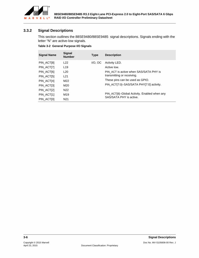
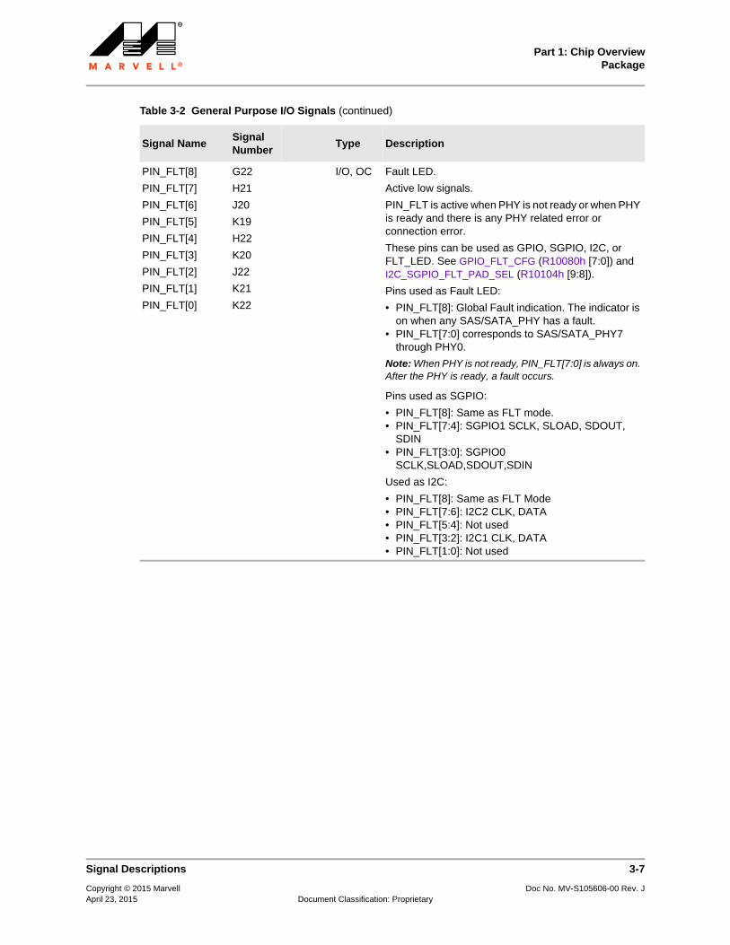
3.3.2 Signal Descriptions
This section outlines the 88SE9480/88SE9485 signal descriptions. Signals ending with the letter “N” are active-low signals.
Table 3-2 General Purpose I/O Signals
Signal NameSignal Number
Type Description
PIN_ACT[8]
PIN_ACT[7]
PIN_ACT[6]
PIN_ACT[5]
PIN_ACT[4]
PIN_ACT[3]
PIN_ACT[2]
PIN_ACT[1]
PIN_ACT[0]
L22
L19
L20
L21
M22
M20
N22
M19
N21
I/O, OC Activity LED.
Active low.
PIN_ACT is active when SAS/SATA PHY is transmitting or receiving.
These pins can be used as GPIO.
PIN_ACT[7:0]–SAS/SATA PHY[7:0] activity.
PIN_ACT[8]–Global Activity. Enabled when any SAS/SATA PHY is active.
Part 1: Chip OverviewPackage
Signal Descriptions 3-7
Copyright © 2015 Marvell Doc No. MV-S105606-00 Rev. JApril 23, 2015 Document Classification: Proprietary
PIN_FLT[8]
PIN_FLT[7]
PIN_FLT[6]
PIN_FLT[5]
PIN_FLT[4]
PIN_FLT[3]
PIN_FLT[2]
PIN_FLT[1]
PIN_FLT[0]
G22
H21
J20
K19
H22
K20
J22
K21
K22
I/O, OC Fault LED.
Active low signals.
PIN_FLT is active when PHY is not ready or when PHY is ready and there is any PHY related error or connection error.
These pins can be used as GPIO, SGPIO, I2C, or FLT_LED. See GPIO_FLT_CFG (R10080h [7:0]) and I2C_SGPIO_FLT_PAD_SEL (R10104h [9:8]).
Pins used as Fault LED:
• PIN_FLT[8]: Global Fault indication. The indicator is on when any SAS/SATA_PHY has a fault.
• PIN_FLT[7:0] corresponds to SAS/SATA_PHY7 through PHY0.
Note: When PHY is not ready, PIN_FLT[7:0] is always on. After the PHY is ready, a fault occurs.
Pins used as SGPIO:
• PIN_FLT[8]: Same as FLT mode.• PIN_FLT[7:4]: SGPIO1 SCLK, SLOAD, SDOUT,
SDIN• PIN_FLT[3:0]: SGPIO0
SCLK,SLOAD,SDOUT,SDIN
Used as I2C:
• PIN_FLT[8]: Same as FLT Mode• PIN_FLT[7:6]: I2C2 CLK, DATA• PIN_FLT[5:4]: Not used• PIN_FLT[3:2]: I2C1 CLK, DATA• PIN_FLT[1:0]: Not used
Table 3-2 General Purpose I/O Signals (continued)
Signal NameSignal Number
Type Description

88SE9480/88SE9485 R3.3 Eight-Lane PCI-Express 2.0 to Eight-Port SAS/SATA 6 Gbps RAID I/O Controller Preliminary Datasheet
3-8 Signal Descriptions
Copyright © 2015 Marvell Doc No. MV-S105606-00 Rev. JApril 23, 2015 Document Classification: Proprietary
PIN_TEST[15]
PIN_TEST[14]
PIN_TEST[13]
PIN_TEST[12]
PIN_TEST[11]
PIN_TEST[10]
PIN_TEST[9]
PIN_TEST[8]
PIN_TEST[7]
PIN_TEST[6]
PIN_TEST[5]
PIN_TEST[4]
PIN_TEST[3]
PIN_TEST[2]
PIN_TEST[1]
PIN_TEST[0]
F19
C21
E20
D21
C22
F20
E21
D22
H19
G20
F21
E22
G21
J19
H20
F22
I/O Configuration and test pins.
These pins can be used as GPIO.
PIN_TEST[15]-PCIe power-up disable
0h: Enable PCIe after power-up1h: Disable PCIe after power-up
Not applicable to this chip. This signal needs pull-down.
PIN_TEST[14:13]–Chip reference clock selection
0h: 20 MHz1h: 50 MHz2h: 100 MHz3h: 75 MHz
PIN_TEST[12:11]–Reserved
PIN_TEST[10]–PCIe ROM location
0h: Parallel Flash1h: Serial Flash
PIN_TEST[9:8]–PCIe maximum lane width
0h: x8
Always use 0h.PIN_TEST[7:6]–Reserved
PIN_TEST[5]—PCIe configuration access enable.
0h: PCIe responds to configuration access.
1h: PCIe returns a retry configuration access.
Not applicable to this chip. This signal needs pull-down.
PIN_TEST[4]–Parallel Flash x8/x16
0h: Byte mode1h: Word mode
PIN_TEST[3:2]–Reserved
PIN_TEST[1]–UART baudrate
0h: 576001h: Reserved
PIN_TEST[0]–UART mode
0h: Reserved1h: Terminal mode
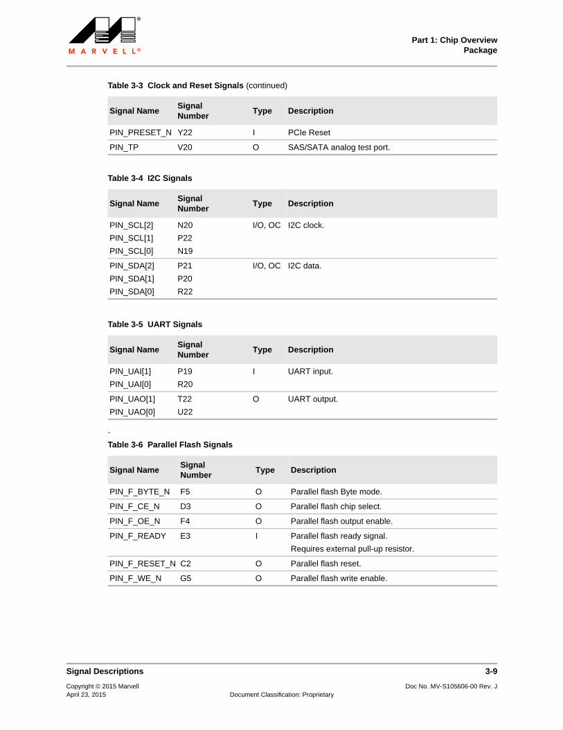
Table 3-3 Clock and Reset Signals
Signal NameSignal Number
Type Description
PIN_REFCLK T19 I Reference clock input.
2.5V, ± 350 ppm.
PIN_RESET_N W22 I Power-on reset.
Table 3-2 General Purpose I/O Signals (continued)
Signal NameSignal Number
Type Description
Part 1: Chip OverviewPackage
Signal Descriptions 3-9
Copyright © 2015 Marvell Doc No. MV-S105606-00 Rev. JApril 23, 2015 Document Classification: Proprietary
.
PIN_PRESET_N Y22 I PCIe Reset
PIN_TP V20 O SAS/SATA analog test port.
Table 3-4 I2C Signals
Signal NameSignal Number
Type Description
PIN_SCL[2]
PIN_SCL[1]
PIN_SCL[0]
N20
P22
N19
I/O, OC I2C clock.
PIN_SDA[2]
PIN_SDA[1]
PIN_SDA[0]
P21
P20
R22
I/O, OC I2C data.
Table 3-5 UART Signals
Signal NameSignal Number
Type Description
PIN_UAI[1]
PIN_UAI[0]
P19
R20
I UART input.
PIN_UAO[1]
PIN_UAO[0]
T22
U22
O UART output.
Table 3-6 Parallel Flash Signals
Signal NameSignal Number
Type Description
PIN_F_BYTE_N F5 O Parallel flash Byte mode.
PIN_F_CE_N D3 O Parallel flash chip select.
PIN_F_OE_N F4 O Parallel flash output enable.
PIN_F_READY E3 I Parallel flash ready signal.
Requires external pull-up resistor.
PIN_F_RESET_N C2 O Parallel flash reset.
PIN_F_WE_N G5 O Parallel flash write enable.
Table 3-3 Clock and Reset Signals (continued)
Signal NameSignal Number
Type Description

88SE9480/88SE9485 R3.3 Eight-Lane PCI-Express 2.0 to Eight-Port SAS/SATA 6 Gbps RAID I/O Controller Preliminary Datasheet
3-10 Signal Descriptions
Copyright © 2015 Marvell Doc No. MV-S105606-00 Rev. JApril 23, 2015 Document Classification: Proprietary
PIN_P_ADDR[21]
PIN_P_ADDR[20]
PIN_P_ADDR[19]
PIN_P_ADDR[18]
PIN_P_ADDR[17]
PIN_P_ADDR[16]
PIN_P_ADDR[15]
PIN_P_ADDR[14]
PIN_P_ADDR[13]
PIN_P_ADDR[12]
PIN_P_ADDR[11]
PIN_P_ADDR[10]
PIN_P_ADDR[9]
PIN_P_ADDR[8]
PIN_P_ADDR[7]
PIN_P_ADDR[6]
PIN_P_ADDR[5]
PIN_P_ADDR[4]
PIN_P_ADDR[3]
PIN_P_ADDR[2]
PIN_P_ADDR[1]]
PIN_P_ADDR[0]
U6
T6
L3
L2
L1
P1
N2
M4
N1
M3
M2
M1
U3
W2
T5
U5
K4
K3
J1
K2
K1
L4
O Shared address bus for parallel flash, NVSRAM and PBSRAM.
For Parallel Flash, signals are word addresses.
For NVSRAM, signals are WORD addresses.
For PBSRAM, signals are Dword addresses.
Table 3-6 Parallel Flash Signals (continued)
Signal NameSignal Number
Type Description
Part 1: Chip OverviewPackage
Signal Descriptions 3-11
Copyright © 2015 Marvell Doc No. MV-S105606-00 Rev. JApril 23, 2015 Document Classification: Proprietary
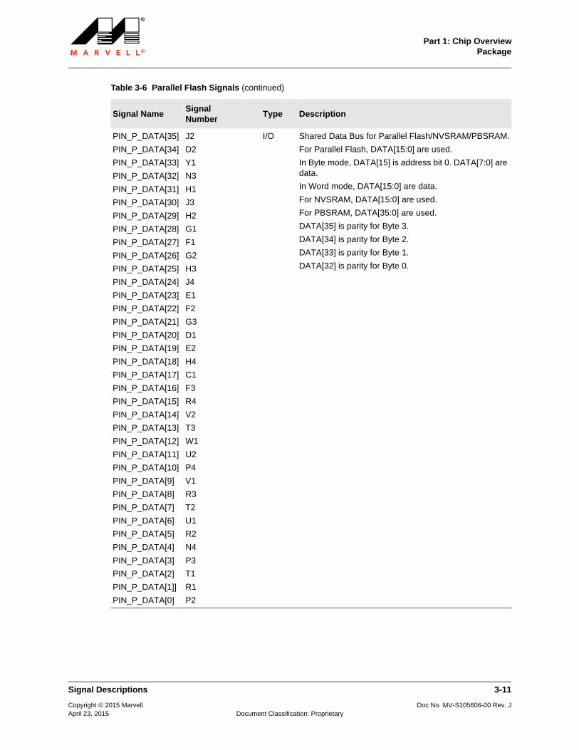
PIN_P_DATA[35]
PIN_P_DATA[34]
PIN_P_DATA[33]
PIN_P_DATA[32]
PIN_P_DATA[31]
PIN_P_DATA[30]
PIN_P_DATA[29]
PIN_P_DATA[28]
PIN_P_DATA[27]
PIN_P_DATA[26]
PIN_P_DATA[25]
PIN_P_DATA[24]
PIN_P_DATA[23]
PIN_P_DATA[22]
PIN_P_DATA[21]
PIN_P_DATA[20]
PIN_P_DATA[19]
PIN_P_DATA[18]
PIN_P_DATA[17]
PIN_P_DATA[16]
PIN_P_DATA[15]
PIN_P_DATA[14]
PIN_P_DATA[13]
PIN_P_DATA[12]
PIN_P_DATA[11]
PIN_P_DATA[10]
PIN_P_DATA[9]
PIN_P_DATA[8]
PIN_P_DATA[7]
PIN_P_DATA[6]
PIN_P_DATA[5]
PIN_P_DATA[4]
PIN_P_DATA[3]
PIN_P_DATA[2]
PIN_P_DATA[1]]
PIN_P_DATA[0]
J2
D2
Y1
N3
H1
J3
H2
G1
F1
G2
H3
J4
E1
F2
G3
D1
E2
H4
C1
F3
R4
V2
T3
W1
U2
P4
V1
R3
T2
U1
R2
N4
P3
T1
R1
P2
I/O Shared Data Bus for Parallel Flash/NVSRAM/PBSRAM.
For Parallel Flash, DATA[15:0] are used.
In Byte mode, DATA[15] is address bit 0. DATA[7:0] are data.
In Word mode, DATA[15:0] are data.
For NVSRAM, DATA[15:0] are used.
For PBSRAM, DATA[35:0] are used.
DATA[35] is parity for Byte 3.
DATA[34] is parity for Byte 2.
DATA[33] is parity for Byte 1.
DATA[32] is parity for Byte 0.
Table 3-6 Parallel Flash Signals (continued)
Signal NameSignal Number
Type Description

88SE9480/88SE9485 R3.3 Eight-Lane PCI-Express 2.0 to Eight-Port SAS/SATA 6 Gbps RAID I/O Controller Preliminary Datasheet
3-12 Signal Descriptions
Copyright © 2015 Marvell Doc No. MV-S105606-00 Rev. JApril 23, 2015 Document Classification: Proprietary
Table 3-7 NVSRAM Signals
Signal NameSignal Number
Type Description
PIN_N_CE_N E4 O nvSRAM chip select.
PIN_N_OE_N G4 O nvSRAM output enable.
PIN_N_WE_N C3 O nvSRAM write enable.
Table 3-8 PBSRAM Signals
Signal NameSignal Number
Type Description
PIN_P_ADSC_N T4 O PBSRAM ASDC mode.
PIN_P_ADV_N V3 O PBSRAM address advance.
PIN_P_BW_N AB2 O PBSRAM BW.
PIN_P_CS1_N V4 O PBSRAM chip select.
PIN_P_GW_N R5 O PBSRAM global write enable.
PIN_P_OE_N AA1 O PBSRAM output enable.
PIN_P_OUT_CLK Y2 O PBSRAM clock.
PIN_P_WE_N[3]
PIN_P_WE_N[2]
PIN_P_WE_N[1]
PIN_P_WE_N[0]
U4
Y3
W3
AA2
O PBSRAM write enable.
Table 3-9 System Interface Signals
Signal NameSignal Number
Type Description
PIN_CNFG[1]
PIN_CNFG[0]
U21
V21
I Configuration.
00: Normal Functional mode.Others:Test Mode.
REFCLKP B12 I PCIe reference clock input.
100MHz ± 300ppm.No internal clock termination.
REFCLKN A12 I PCIe reference clock input.
100MHz ± 300ppm.No internal clock termination.

Part 1: Chip OverviewPackage
Signal Descriptions 3-13
Copyright © 2015 Marvell Doc No. MV-S105606-00 Rev. JApril 23, 2015 Document Classification: Proprietary
Table 3-10 SPI Interface Signals
Signal NameSignal Number
Type Description
PIN_SPI_DI T21 I SPI data input.
PIN_SPI_CLK V22 O SPI clock.
PIN_SPI_CS_N R19 O SPI chip select.
PIN_SPI_DO T20 O SPI data output.
Table 3-11 PCIe Interface Signals
Signal NameSignal Number
Type Description
ISET U18 I/O Reference Current for PCI-Express PHY.
This pin must be connected to an external 6.04 kΩ, 1% resistor to ground.
PIN_ISET E12 I Chip reference resistor 5 kΩ.
PTP E14 O Analog test port for PCIe.
PIN_M_CLK U20 I PCIe debugging MDIO interface, clock.
PIN_M_DATA W21 I/O PCIe debugging MDIO interface, data.
Table 3-12 SAS/SATA Transmitter and Receiver Interface Signals
Signal NameSignal Number
Type Description
PIN_RXP[7]
PIN_RXP[6]
PIN_RXP[5]
PIN_RXP[4]
PIN_RXP[3]
PIN_RXP[2]
PIN_RXP[1]
PIN_RXP[0]
AB18
AB16
AB14
AB12
AB10
AA8
W7
W5
–
–
–
–
I PIN_RXP[7:0]–SAS/SATA PHY 7–0 Receiver Differential Signal.
PIN_RXN[7]
PIN_RXN[6]
PIN_RXN[5]
PIN_RXN[4]
PIN_RXN[3]
PIN_RXN[2]
PIN_RXN[1]
PIN_RXN[0]
AA18
AA16
AA14
AA12
AA10
AB8
Y7
Y5
–
–
–
–
I PIN_RXN[7:0]–SAS/SATA PHY 7–0 Receiver Differential Signals.

88SE9480/88SE9485 R3.3 Eight-Lane PCI-Express 2.0 to Eight-Port SAS/SATA 6 Gbps RAID I/O Controller Preliminary Datasheet
3-14 Signal Descriptions
Copyright © 2015 Marvell Doc No. MV-S105606-00 Rev. JApril 23, 2015 Document Classification: Proprietary
PIN_TXP[7]
PIN_TXP[6]
PIN_TXP[5]
PIN_TXP[4]
PIN_TXP[3]
PIN_TXP[2]
PIN_TXP[1]
PIN_TXP[0]
W19
W17
W15
W13
W11
Y9
AB6
AB4
–
–
–
–
O PIN_TXP[7:0]–SAS/SATA PHY 7–0 Transmitter Differential Signals.
PIN_TXN[7]
PIN_TXN[6]
PIN_TXN[5]
PIN_TXN[4]
PIN_TXN[3]
PIN_TXN[2]
PIN_TXN[1]
PIN_TXN[0]
Y19
Y17
Y15
Y13
Y11
W9
AA6
AA4
O PIN_TXN[7:0]–SAS/SATA PHY 7–0 Transmitter Differential Signals.
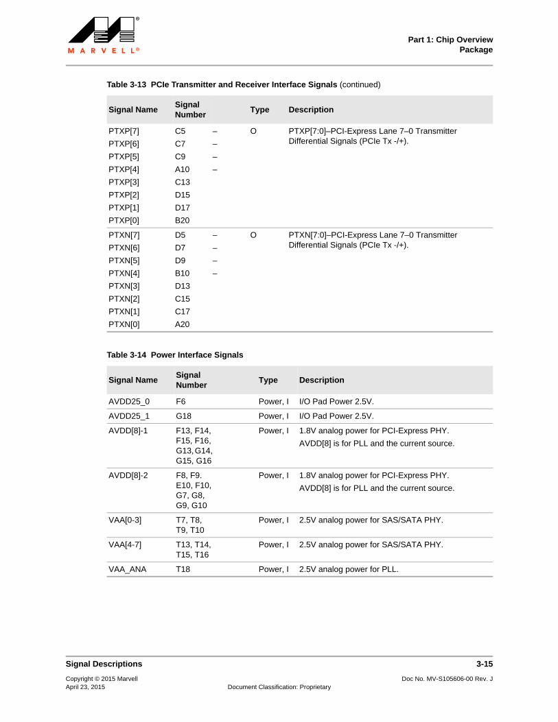
Table 3-13 PCIe Transmitter and Receiver Interface Signals
Signal NameSignal Number
Type Description
PRXP[7]
PRXP[6]
PRXP[5]
PRXP[4]
PRXP[3]
PRXP[2]
PRXP[1]
PRXP[0]
B4
B6
B8
D11
A14
A16
A18
C19
–
–
–
–
I PRXP[7:0]–PCI-Express Lane 7–0 Receiver Differential Signal (PCIe Rx +/-).
PRXN[7]
PRXN[6]
PRXN[5]
PRXN[4]
PRXN[3]
PRXN[2]
PRXN[1]
PRXN[0]
A4
A6
A8
C11
B14
B16
B18
D19
–
–
–
–
I PRXN[7:0]–PCI-Express Lane 7–0 Receiver Differential Signals (PCIe Rx +/-).
Table 3-12 SAS/SATA Transmitter and Receiver Interface Signals (continued)
Signal NameSignal Number
Type Description
Part 1: Chip OverviewPackage
Signal Descriptions 3-15
Copyright © 2015 Marvell Doc No. MV-S105606-00 Rev. JApril 23, 2015 Document Classification: Proprietary
PTXP[7]
PTXP[6]
PTXP[5]
PTXP[4]
PTXP[3]
PTXP[2]
PTXP[1]
PTXP[0]
C5
C7
C9
A10
C13
D15
D17
B20
–
–
–
–
O PTXP[7:0]–PCI-Express Lane 7–0 Transmitter Differential Signals (PCIe Tx -/+).
PTXN[7]
PTXN[6]
PTXN[5]
PTXN[4]
PTXN[3]
PTXN[2]
PTXN[1]
PTXN[0]
D5
D7
D9
B10
D13
C15
C17
A20
–
–
–
–
O PTXN[7:0]–PCI-Express Lane 7–0 Transmitter Differential Signals (PCIe Tx -/+).
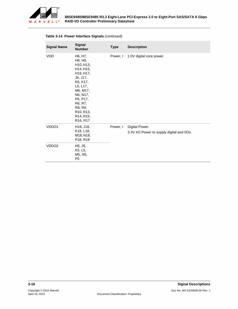
Table 3-14 Power Interface Signals
Signal NameSignal Number
Type Description
AVDD25_0 F6 Power, I I/O Pad Power 2.5V.
AVDD25_1 G18 Power, I I/O Pad Power 2.5V.
AVDD[8]-1 F13, F14, F15, F16, G13, G14, G15, G16
Power, I 1.8V analog power for PCI-Express PHY.
AVDD[8] is for PLL and the current source.
AVDD[8]-2 F8, F9. E10, F10, G7, G8, G9, G10
Power, I 1.8V analog power for PCI-Express PHY.
AVDD[8] is for PLL and the current source.
VAA[0-3] T7, T8, T9, T10
Power, I 2.5V analog power for SAS/SATA PHY.
VAA[4-7] T13, T14, T15, T16
Power, I 2.5V analog power for SAS/SATA PHY.
VAA_ANA T18 Power, I 2.5V analog power for PLL.
Table 3-13 PCIe Transmitter and Receiver Interface Signals (continued)
Signal NameSignal Number
Type Description
88SE9480/88SE9485 R3.3 Eight-Lane PCI-Express 2.0 to Eight-Port SAS/SATA 6 Gbps RAID I/O Controller Preliminary Datasheet
3-16 Signal Descriptions
Copyright © 2015 Marvell Doc No. MV-S105606-00 Rev. JApril 23, 2015 Document Classification: Proprietary
VDD H6, H7, H8, H9, H10, H13, H14, H15, H16, H17, J6, J17, K6, K17, L6, L17, M6, M17, N6, N17, P6, P17, R6, R7, R8, R9, R10, R13, R14, R15, R16, R17
Power, I 1.0V digital core power.
VDDO1 H18, J18, K18, L18, M18, N18, P18, R18
Power, I Digital Power.
3.3V I/O Power to supply digital and I/Os.
VDDO2 H5, J5, K5, L5, M5, N5, P5
Table 3-14 Power Interface Signals (continued)
Signal NameSignal Number
Type Description

Part 1: Chip OverviewPackage
Signal Descriptions 3-17
Copyright © 2015 Marvell Doc No. MV-S105606-00 Rev. JApril 23, 2015 Document Classification: Proprietary
VSS A1, A2, A3, A5, A7, A9, A11, A13, A15, A17, A19, A21, A22, AA3, AA5, AA7, AA9, AA11, AA13, AA15, AA17, AA19–AA22, AB1, AB3, AB5, AB7, AB9, AB11, AB13, AB15, AB17, AB19–AB22, B1, B2, B3, B5, B7, B9, B11, B13, B15, B17, B19, B21, B22, C4, C6, C8, C10, C12, C14, C16, C18, C20, D4, D6, D8, D10, D12, D14, D16, D18, D20, E5, E6, E7, E8, E9, E11, E13, E15, E16, E17, E18, E19, F7, F11, F12, F17, F18, G6, G11, G12, G17, G19, H11, H12
Ground Ground.
Table 3-14 Power Interface Signals (continued)
Signal NameSignal Number
Type Description

88SE9480/88SE9485 R3.3 Eight-Lane PCI-Express 2.0 to Eight-Port SAS/SATA 6 Gbps RAID I/O Controller Preliminary Datasheet
3-18 Signal Descriptions
Copyright © 2015 Marvell Doc No. MV-S105606-00 Rev. JApril 23, 2015 Document Classification: Proprietary
VSS J7–J16, J21, K7–K16, L7–L16, M7–M16, M21, N7–N16, P7–P16, R11, R12, R21, T11, T12, T17, U7–U17, U19, V5–V19, W4, W6, W8, W10, W12, W14, W16, W18, W20, Y4, Y6, Y8, Y10, Y12, Y14, Y16, Y18, Y20, Y21
Ground Ground.
Table 3-14 Power Interface Signals (continued)
Signal NameSignal Number
Type Description

Part 1: Chip OverviewLayout Guidelines
4-1
Copyright © 2015 Marvell Doc No. MV-S105606-00 Rev. JApril 23, 2015 Document Classification: Proprietary
4 LAYOUT GUIDELINES
This chapter describes the system recommendations from the Marvell Semiconductor design and application engineers who work with the 88SE9480/88SE9485. It is written for those who are designing schematics and printed circuit boards for an 88SE9480/88SE9485-based system. Whenever possible, the PCB designer should try to follow the suggestions provided in this chapter.
The information in this chapter is preliminary. Please consult with Marvell Semiconductor design and application engineers before starting your PCB design.
This chapter contains the following sections:
88SE9480/88SE9485 Board Schematics
Layer Stack-Up
Power Supply
PCB Trace Routing
Recommended Layout
Refer to Chapter 3, Package, for package information.

88SE9480/88SE9485 R3.3 Eight-Lane PCI-Express 2.0 to Eight-Port SAS/SATA 6 Gbps RAID I/O Controller Preliminary Datasheet
4-2 88SE9480/88SE9485 Board Schematics
Copyright © 2015 Marvell Doc No. MV-S105606-00 Rev. JApril 23, 2015 Document Classification: Proprietary
4.1 88SE9480/88SE9485 Board Schematics
This section contains board schematics for the 88SE9480/88SE9485.
It contains the following figures:
Figure 4-1, 88SE9480/88SE9485 PCIe and SAS
Figure 4-2, 88SE9480/88SE9485 Bootstrap, NI, SPI, UART, I2C, LED
Figure 4-3, 88SE9480/88E9485 Power and Ground

Part 1: Chip OverviewLayout Guidelines
88SE9480/88SE9485 Board Schematics 4-3
Copyright © 2015 Marvell Doc No. MV-S105606-00 Rev. JApril 23, 2015 Document Classification: Proprietary
Figure 4-4, 88SE9480/88SE9485 Power Regulators
Figure 4-1 88SE9480/88SE9485 PCIe and SAS
CNFG[1:0]
(INT
ERNA
L TE
ST M
ODE
SELE
CTIO
N)
01:
10:
11:
*00: Normal
SRXN
0
STXN
1
SRXN
1
SRXN
2
STXN
2
SRXN
3
STXN
3
STXN
4
SRXN
4
SRXN
5
STXN
5
STXN
6
SRXN
6
S_TX
P7
S_R
XN7
STXN
7
SRXN
7
S_R
XN3
PRXN
7PR
XP7
PRXN
6PR
XP6
PRXN
5PR
XP5
PRXN
4PR
XP4
HSI
N7
PTXN
7
HSI
P7PT
XP7
PTXN
6
HSI
P6
HSI
N5
PTXN
5
HSI
P5PT
XP5
HSI
N4
PTXN
4
HSI
P4PT
XP4
HSI
N3
PTXN
3
HSI
P3PT
XP3
HSI
N2
PTXN
2
HSI
P2PT
XP2
HSI
N1
PTXN
1
HSI
P1PT
XP1
HSI
N0
PTXN
0
HSI
P0PT
XP0
PTXN
0PT
XP0
PCIE
_RES
ET
PCLK
N
PCLK
P
PCLK
NPC
LKP
CN
FG0
CN
FG1
STXP
0
STXN
0
PTXN
6PT
XP6
PTXN
5PT
XP5
PTXN
4PT
XP4
PTXN
7PT
XP7
PTXN
3PT
XP3
PTXN
2PT
XP2
PTXN
1PT
XP1
PRXN
0PR
XP0
PRXN
1PR
XP1
PRXN
2PR
XP2
PRXN
3PR
XP3
3V3_
PCIE
S_TX
P0
S_TX
N0
S_R
XN0
S_R
XP0
SRXP
0
S_TX
P1ST
XP1
S_TX
N1
S_R
XN1
S_R
XP1
SRXP
1
S_TX
P2ST
XP2
S_TX
N2
S_R
XN2
S_R
XP2
SRXP
2
S_TX
P3
S_TX
N3
S_R
XN3
S_R
XP3
STXP
3
SRXP
3
S_TX
N4
STXP
4
SRXP
4S_
RXP
4
S_TX
P5
S_TX
N5
S_R
XN5
S_R
XP5
STXP
5
SRXP
5
S_TX
P6
S_TX
N6
S_R
XN6
S_R
XP6
STXP
6
SRXP
6
S_TX
N7
S_R
XP7
STXP
7
SRXP
7
PTXP
6H
SIN
6
STXP
5ST
XN5
STXN
2ST
XP2
STXN
6ST
XP6
STXN
7ST
XP7
SRXP
2SR
XN2
SRXN
0SR
XP0
STXN
3ST
XP3
SRXP
3SR
XN3
STXP
0ST
XN0
SRXP
4SR
XN4
SRXP
5SR
XN5
SRXP
6SR
XN6
SRXP
7SR
XN7
STXN
1ST
XP1
STXN
4ST
XP4
SRXP
1SR
XN1
S_R
XP7
S_R
XN7
S_TX
N7
S_TX
P7
S_R
XP6
S_R
XN6
S_TX
N6
S_TX
P6
S_R
XP5
S_R
XN5
S_TX
N5
S_TX
P5
S_R
XP4
S_R
XN4
S_R
XN4
S_TX
N4
S_TX
P4S_
TXP4
S_R
XP3
S_TX
N3
S_TX
P3
S_R
XP2
S_R
XN2
S_TX
N2
S_TX
P2
S_R
XP1
S_R
XN1
S_TX
N1
S_TX
P1
S_R
XP0
S_R
XN0
S_TX
N0
S_TX
P0
S_D
IN1
S_D
OU
T1
S_LO
AD1
S_C
LK1
S_D
IN0
S_LO
AD0
S_C
LK0
S_D
OU
T0
3V3
12V0
12V0
3V3
2V5
S_D
IN0
3
S_C
LK0
3S_
LOAD
03
S_D
OU
T03
S_D
IN1
3
S_LO
AD1
3
S_D
OU
T13
S_C
LK1
3
PCIE
_RES
ET3
C20
0.1U
C15
0.01
U
C32
0.1U
C46
0.01
U
C13
0.1U
C175 1000pF_X
C29
0.01
U
C11
7
4.7U
R21
100R
_X
C3
0.01
U
C178 1000pF_X
C51
0.1U
C35
0.01
U
C36
0.01
U
CFG
1_0
1K
C174 1000pF_X
C34
0.01
U
C176 1000pF_X
PCIE x8
TOP
BOT
P1
PCIE
x8_G
old_
Fing
er
+12V
_3B
1+1
2V_4
B2
RS
VD
_4B
3G
ND
_19
B4
SM
CLK
B5
SM
DA
TB
6G
ND
_20
B7
3V3_
3B
8TR
ST#
B9
3.3V
Aux
B10
WA
KE
#B
11
RS
VD
_5B
12G
ND
_21
B13
HS
Op(
0)B
14H
SO
n(0)
B15
GN
D_2
2B
16P
RS
NT#
2AB
17G
ND
_23
B18
HS
Op(
1)B
19H
SO
n(1)
B20
GN
D_2
4B
21G
ND
_25
B22
HS
Op(
2)B
23H
SO
n(2)
B24
GN
D_2
6B
25G
ND
_27
B26
HS
Op(
3)B
27H
SO
n(3)
B28
GN
D_2
8B
29R
SV
D_6
B30
PR
SN
T#2B
B31
GN
D_2
9B
32
PR
SN
T#1
A1
+12V
_1A
2+1
2V_2
A3
GN
D_1
A4
TCK
A5
TDI
A6
TDO
A7
TMS
A8
3V3_
1A
93V
3_2
A10
PW
RG
DA
11
GN
D_2
A12
RE
FCLK
+A
13R
EFC
LK-
A14
GN
D_3
A15
HS
Ip(0
)A
16H
SIn
(0)
A17
GN
D_4
A18
RS
VD
_1A
19G
ND
_5A
20H
SIp
(1)
A21
HS
In(1
)A
22G
ND
_6A
23G
ND
_7A
24H
SIp
(2)
A25
HS
In(2
)A
26G
ND
_8A
27G
ND
_9A
28H
SIp
(3)
A29
HS
In(3
)A
30G
ND
_10
A31
RS
VD
_2A
32R
SV
D_3
A33
HS
Ip(4
)A
35H
SIn
(4)
A36
GN
D_1
2A
37G
ND
_13
A38
HS
Ip(5
)A
39H
SIn
(5)
A40
GN
D_1
4A
41G
ND
_15
A42
GN
D_1
1A
34
HS
Ip(6
)A
43H
SIn
(6)
A44
GN
D_1
6A
45G
ND
_17
A46
HS
Ip(7
)A
47H
SIn
(7)
A48
GN
D_1
8A
49
HS
Op(
4)B
33H
SO
n(4)
B34
GN
D_3
0B
35G
ND
_31
B36
HS
Op(
5)B
37H
SO
n(5)
B38
GN
D_3
2B
39G
ND
_33
B40
HS
Op(
6)B
41H
SO
n(6)
B42
GN
D_3
4B
43G
ND
_35
B44
HS
Op(
7)B
45H
SO
n(7)
B46
GN
D_3
6B
47P
RS
NT#
2CB
48G
ND
_37
B49
C40
0.01
U
C8
0.01
U
C41
0.01
U
TP39
1
C39
0.01
U
C173 1000pF_X
C44
0.01
U
C6
0.01
U
C47
0.01
U
C1
0.01
U
C43
0.01
U
C26
0.01
U
FB1
FB_1
A
12
CFG
1_1
10K_
X
C49
0.1U
C16
0.1U
C9
0.01
U
C37
0.01
U
C7
0.1U
C18
0.01
U
C22
0.1U
Y1
50M
HZ_
8W50
0000
02
OE
1
OU
T3
Vcc
4
GN
D2
C177 1000pF_X
C10
0.01
U
C24
0.1U
C28
0.1U
C17
0.01
U
R22
6.04
K
C2
0.01
U
C30
0.01
U
C5
0.1U
C50 1U
C42
0.01
U
C171 1000pF_X
C21
0.1U
C56
0.1U
J1
iPAS
S_0.
8mm
_36
conn
32_m
inis
as_s
md_
36_0
1_pa
ste
RX
+0A
2
RX
+1A
5
RX
+2A
13
RX
+3A
16
RX
-0A
3
RX
-1A
6
RX
-2A
14
RX
-3A
17
TX+0
B2
TX+1
B5
TX+2
B13
TX+3
B16
TX-0
B3
TX-1
B6
TX-2
B14
TX-3
B17
GN
D1
A1
GN
D2
A4
GN
D3
A7
GN
D4
A12
GN
D5
A15
GN
D6
A18
GN
D7
B1
GN
D8
B4
GN
D9
B7
GN
D10
B12
PE
G1
H1
PE
G2
H2
MTH
1H
3
MTH
2H
4
MTH
3H
5
MTH
4H
6
MTH
5H
7
MTH
6H
8
SB
0-S
CLK
B8
SB
1-S
LOD
B9
SB
2-G
ND
B10
SB
3A
9
SB
4_S
DO
A10
SB
5_S
DI
A11
SB
6B
11
SB
7A
8
GN
D11
B15
GN
D12
B18
C172 1000pF_X
C14
0.1U
C11
0.1U
C38
0.01
U
C27
0.1U
C25
0.01
U
C31
0.1U
R20
4.99
K
CFG
0_0
1K
C23
0.1U
C59 1U
C45
0.01
U
C33
0.01
U
PEX
CLOCK & RESET
SAS/SATA
U1A 88SE
9480
/88S
E948
5
PIN
_CN
FG[1
]U
21P
IN_C
NFG
[0]
V21
PIN
_TP
V20
PIN
_RX
P[0
]W
5
PIN
_RX
P[1
]W
7
PIN
_TX
N[2
]W
9
PIN
_TX
P[3
]W
11
PIN
_TX
P[4
]W
13
PIN
_TX
P[5
]W
15
PIN
_TX
P[6
]W
17
PIN
_TX
P[7
]W
19
PIN
_RX
N[0
]Y
5
PIN
_RX
N[1
]Y
7
PIN
_TX
P[2
]Y
9
PIN
_TX
N[3
]Y
11
PIN
_TX
N[4
]Y
13
PIN
_TX
N[5
]Y
15
PIN
_TX
N[6
]Y
17
PIN
_TX
N[7
]Y
19
PIN
_TX
N[0
]A
A4
PIN
_TX
N[1
]A
A6
PIN
_RX
P[2
]A
A8
PIN
_RX
N[3
]A
A10
PIN
_RX
N[4
]A
A12
PIN
_RX
N[5
]A
A14
PIN
_RX
N[6
]A
A16
PIN
_RX
N[7
]A
A18
PIN
_TX
P[0
]A
B4
PIN
_TX
P[1
]A
B6
PIN
_RX
N[2
]A
B8
PIN
_RX
P[3
]A
B10
PIN
_RX
P[4
]A
B12
PIN
_RX
P[5
]A
B14
PIN
_RX
P[6
]A
B16
PIN
_RX
P[7
]A
B18
PR
XN
[7]
A4
PR
XN
[6]
A6
PR
XP
[7]
B4
PR
XP
[6]
B6
PR
XN
[5]
A8
PR
XN
[4]
C11
PR
XN
[3]
B14
PR
XP
[2]
A16
PR
XP
[1]
A18
PR
XP
[0]
C19
PR
XP
[5]
B8
PR
XP
[4]
D11
PR
XP
[3]
A14
PR
XN
[2]
B16
PR
XN
[1]
B18
PR
XN
[0]
D19
PIN
_PR
ES
ET_
NY
22
PIN
_IS
ET
E12
RE
FCLK
PB
12R
EFC
LKN
A12
ISE
TU
18
PTX
N[7
]D
5
PTX
P[7
]C
5
PTX
N[6
]D
7
PTX
P[6
]C
7
PTX
N[5
]D
9
PTX
P[5
]C
9
PTX
N[4
]B
10
PTX
P[4
]A
10
PTX
N[3
]D
13
PTX
P[3
]C
13
PTX
N[2
]C
15
PTX
P[2
]D
15
PTX
N[1
]C
17
PTX
P[1
]D
17
PTX
N[0
]A
20
PTX
P[0
]B
20
PIN
_RE
SE
T_N
W22
PIN
_RE
FCLK
T19
PTP
E14
C19
0.01
U
CFG
0_1
10K_
X
J2
iPAS
S_0.
8mm
_36
conn
32_m
inis
as_s
md_
36_0
1_pa
ste
RX
+0A
2
RX
+1A
5
RX
+2A
13
RX
+3A
16
RX
-0A
3
RX
-1A
6
RX
-2A
14
RX
-3A
17
TX+0
B2
TX+1
B5
TX+2
B13
TX+3
B16
TX-0
B3
TX-1
B6
TX-2
B14
TX-3
B17
GN
D1
A1
GN
D2
A4
GN
D3
A7
GN
D4
A12
GN
D5
A15
GN
D6
A18
GN
D7
B1
GN
D8
B4
GN
D9
B7
GN
D10
B12
PE
G1
H1
PE
G2
H2
MTH
1H
3
MTH
2H
4
MTH
3H
5
MTH
4H
6
MTH
5H
7
MTH
6H
8
SB
0-S
CLK
B8
SB
1-S
LOD
B9
SB
2-G
ND
B10
SB
3A
9
SB
4_S
DO
A10
SB
5_S
DI
A11
SB
6B
11
SB
7A
8
GN
D11
B15
GN
D12
B18
TP1
1
R1
0R
C48
0.01
U
C4
0.01
U
C12
0.1U

88SE9480/88SE9485 R3.3 Eight-Lane PCI-Express 2.0 to Eight-Port SAS/SATA 6 Gbps RAID I/O Controller Preliminary Datasheet
4-4 88SE9480/88SE9485 Board Schematics
Copyright © 2015 Marvell Doc No. MV-S105606-00 Rev. JApril 23, 2015 Document Classification: Proprietary
Note: This diagram is for reference only. Contact your Marvell field applications engineer for the latest schematics.
Figure 4-2 88SE9480/88SE9485 Bootstrap, NI, SPI, UART, I2C, LED
5 5
4 4
3 3
2 2
1 1
DD
CC
BB
AA
PIN_TEST[15:0]
Configuration and Test pins, GPIO.
PIN_TEST[15] => Must tie low
PIN_TEST[14:13] => Chip reference clock selection
PIN_TEST[12:11] => RSVD
PIN_TEST[10] => PCIE ROM Location
PIN_TEST[9:8] => RSVD
PIN_TEST[7:5] => Must tie low
PIN_TEST[4] => Parallel Flash x8/x16 =>
PIN_TEST[3:2] => RSVD
PIN_TEST[1] => UART Baud Rate =>
PIN_TEST[0] => UART Mode =>
00: 20MHz, 01: 50MHz(default),
0: Parallel Flash, 1: Serial Flash
00 or 11
0: Byte Mode, 1: Word Mode
0: 57600, 1: RSVD
0: RSVD, 1: Terminal Mode
(DRIVE FAULT LED)
SPI FLASH, 4MBit
(ACTIVITY LED)
NVRAM 32KB
pin 2: NC, pin47: NC
NVRAM 128KB
pin 2: A16, pin47: A15
UART
Drive Fault/ Activity LED headers
Top - Activity (Green)
Bottom - Fault (Yellow)
I2C connector
BUZZER
ON
BUZZER
Install R49, 10K and R54, 1K for debug purposes (UART)
(ACTIVITY LED)
(DRIVE FAULT LED)
000
010: 100MHz, 11: 75MHz
ACT2
ACT3
ACT0
ACT1
ACT4
ACT6
ACT7
ACT5
S_D
IN0
S_LO
AD0
S_C
LK0
S_D
IN1
S_D
OU
T1S_
LOAD
1S_
CLK
1FL
T8
P_AD
DR
0P_
ADD
R1
P_AD
DR
2P_
ADD
R3
P_AD
DR
4P_
ADD
R5
P_AD
DR
6P_
ADD
R7
P_AD
DR
8P_
ADD
R9
P_AD
DR
10P_
ADD
R11
P_AD
DR
12P_
ADD
R13
P_AD
DR
14P_
ADD
R15
P_AD
DR
16
P_D
ATA0
P_D
ATA1
P_D
ATA2
P_D
ATA3
P_D
ATA4
P_D
ATA5
P_D
ATA6
P_D
ATA7
TEST
[0]
TEST
[1]
TEST
[2]
TEST
[3]_
FLT2
TEST
[4]_
FLT3
TEST
[5]
TEST
[7]_
FLT5
TEST
[8]
TEST
[9]
TEST
[10]
TEST
[11]
_FLT
6TE
ST[1
2]_F
LT7
TEST
[13]
TEST
[14]
TEST
[15]
UAO
_0
UAI
_0
N_W
E_N
N_C
E_N
N_O
E_N
SPI_
CLK
SPI_
CS_
N
TEST
[10]
TEST
[0]
SPI_
DO
SPI_
DI
TEST
[13]
TEST
[14]
ACT2
ACT3
ACT0
ACT1
ACT4
ACT6
ACT7
ACT5
M_C
LKM
_DAT
A
N_W
E_N
P_AD
DR
13P_
ADD
R8
P_AD
DR
9
P_AD
DR
15
P_AD
DR
11
N_C
E_N
P_D
ATA6
P_AD
DR
10
P_D
ATA7
P_D
ATA5
P_D
ATA4
P_D
ATA3
P_D
ATA0
P_AD
DR
3P_
ADD
R2
P_AD
DR
1P_
ADD
R0
P_AD
DR
16P_
ADD
R14
P_AD
DR
12P_
ADD
R7
P_AD
DR
6P_
ADD
R5
N_O
E_N
P_AD
DR
4
P_D
ATA1
P_D
ATA2
UAI
_0U
AO_0
ACT8
SMD
ATI2
C_S
DA
SMC
LKI2
C_S
CL
I2C
_SD
AI2
C_S
CL
SPI_
DI
SPI_
DO
SPI_
CLK
SPI_
CS_
N
TEST
[2]
TEST
[1]
TEST
[3]_
FLT2
TEST
[6]_
FLT4
TEST
[7]_
FLT5
TEST
[4]_
FLT3
TEST
[12]
_FLT
7TE
ST[1
1]_F
LT6
ACT2
ACT3
ACT0
ACT1
ACT4
ACT6
ACT7
ACT5
TEST
[3]_
FLT2
TEST
[6]_
FLT4
TEST
[7]_
FLT5
TEST
[4]_
FLT3
TEST
[12]
_FLT
7TE
ST[1
1]_F
LT6
FLT0
FLT1
S_D
OU
T0
FLT1
FLT0
TEST
[6]_
FLT4
3V3
3V3
3V3
3V3
3V3
3V3
3V3
3V3
3V3
3V3
3V3
3V3
3V3
12V0
3V3
3V3
S_D
IN0
2
S_LO
AD0
2S_
DO
UT0
2
S_C
LK0
2
S_D
IN1
2
S_LO
AD1
2S_
DO
UT1
2
S_C
LK1
2
TP5
1
TP121 1
TP82
1
TP96
1
TP11
51
R11
210
0R
Q4
sot2
3N
PN
600m
A1
23
R54
1K
U6
W25
X40A
VSN
IGC
S1
SO
2
WP
3S
I5
SC
K6
HO
LD7
VC
C8
GN
D4
U5 CY1
4B25
6LA-
SP25
XIT
Vca
p1
A16
2
A14
3
A12
4
A7
5
A6
6
A5
7
NC
18
A4
9
NC
210
NC
311
NC
412
VS
S1
13
NC
514
NC
615
DQ
016
A3
17
A2
18
A1
19
A0
20
DQ
121
DQ
222
NC
723
NC
824
VS
S2
36N
C11
37N
C12
38N
C13
39A
1140
NC
1441
A9
42A
843
A13
44
NC
1035
NC
934
DQ
633
OE
#32
A10
31
CE
#30
VC
C2
48
A15
47
HS
B#
46
WE
#45
DQ
729
DQ
528
DQ
427
DQ
326
VC
C1
25
TP11
31
FLT5
Ambe
r
NVSRAM/FLASH
CONFIG/TEST/RSVD
PBSRAM
SERIAL INTERFACE
LED
U1B 88SE
9480
/88S
E948
5
PIN
_UA
O[0
]U
22
PIN
_UA
O[1
]T
22
PIN
_UA
I[0]
R20
PIN
_UA
I[1]
P19
PIN
_FLT
[0]
K22
PIN
_FLT
[1]
K21
PIN
_FLT
[2]
J22
PIN
_FLT
[3]
K20
PIN
_FLT
[4]
H22
PIN
_FLT
[5]
K19
PIN
_FLT
[6]
J20
PIN
_FLT
[7]
H21
PIN
_FLT
[8]
G22
PIN
_SP
I_D
IT
21
PIN
_SP
I_D
OT
20
PIN
_SP
I_C
LKV
22
PIN
_SP
I_C
S_N
R19
PIN
_N_W
E_N
C3
PIN
_N_C
E_N
E4
PIN
_N_O
E_N
G4
PIN
_P_A
DD
R[0
]L4
PIN
_P_A
DD
R[1
]K
1
PIN
_P_A
DD
R[2
]K
2
PIN
_P_A
DD
R[3
]J1
PIN
_P_A
DD
R[4
]K
3
PIN
_P_A
DD
R[5
]K
4
PIN
_P_A
DD
R[6
]U
5
PIN
_P_A
DD
R[7
]T
5
PIN
_P_A
DD
R[8
]W
2
PIN
_P_A
DD
R[9
]U
3
PIN
_P_A
DD
R[1
0]M
1
PIN
_P_A
DD
R[1
1]M
2
PIN
_P_A
DD
R[1
2]M
3
PIN
_P_A
DD
R[1
4]M
4P
IN_P
_AD
DR
[13]
N1
PIN
_P_A
DD
R[1
5]N
2
PIN
_P_A
DD
R[1
6]P
1
PIN
_P_A
DD
R[1
7]L1
PIN
_P_A
DD
R[1
8]L2
PIN
_P_A
DD
R[1
9]L3
PIN
_P_A
DD
R[2
0]T
6
PIN
_P_A
DD
R[2
1]U
6
PIN
_P_B
W_N
AB
2
PIN
_P_O
UT
_CLK
Y2
PIN
_P_O
E_N
AA
1
PIN
_P_C
S1_
NV
4
PIN
_P_W
E_N
[0]
AA
2
PIN
_P_W
E_N
[1]
W3
PIN
_P_W
E_N
[2]
Y3
PIN
_P_W
E_N
[3]
U4
PIN
_P_D
AT
A[0
]P
2
PIN
_P_D
AT
A[1
]R
1
PIN
_P_D
AT
A[2
]T
1
PIN
_P_D
AT
A[3
]P
3
PIN
_P_D
AT
A[4
]N
4
PIN
_P_D
AT
A[5
]R
2
PIN
_P_D
AT
A[6
]U
1
PIN
_P_D
AT
A[7
]T
2
PIN
_P_D
AT
A[8
]R
3
PIN
_P_D
AT
A[9
]V
1
PIN
_P_D
AT
A[1
0]P
4
PIN
_P_D
AT
A[1
1]U
2
PIN
_P_D
AT
A[1
2]W
1
PIN
_P_D
AT
A[1
3]T
3
PIN
_P_D
AT
A[1
4]V
2
PIN
_P_D
AT
A[1
5]R
4
PIN
_P_D
AT
A[1
6]F3
PIN
_P_D
AT
A[1
7]C
1
PIN
_P_D
AT
A[1
8]H
4
PIN
_P_D
AT
A[1
9]E
2
PIN
_P_D
AT
A[2
0]D
1
PIN
_P_D
AT
A[2
1]G
3
PIN
_P_D
AT
A[2
2]F2
PIN
_P_D
AT
A[2
3]E
1
PIN
_P_D
AT
A[2
4]J4
PIN
_P_D
AT
A[2
5]H
3
PIN
_P_D
AT
A[2
6]G
2
PIN
_P_D
AT
A[2
7]F1
PIN
_P_D
AT
A[2
8]G
1
PIN
_P_D
AT
A[2
9]H
2
PIN
_P_D
AT
A[3
0]J3
PIN
_P_D
AT
A[3
1]H
1
PIN
_P_D
AT
A[3
2]N
3
PIN
_P_D
AT
A[3
3]Y
1
PIN
_P_D
AT
A[3
4]D
2
PIN
_P_D
AT
A[3
5]J2
PIN
_P_G
W_N
R5
PIN
_P_A
DS
C_N
T4
PIN
_P_A
DV
_NV
3
PIN
_F_R
ES
ET
_NC
2
PIN
_F_C
E_N
D3
PIN
_F_R
EA
DY
E3
PIN
_F_W
E_N
G5
PIN
_F_O
E_N
F4
PIN
_F_B
YT
E_N
F5
PIN
_SD
A[0
]R
22
PIN
_SD
A[1
]P
20
PIN
_SD
A[2
]P
21
PIN
_SC
L[0]
N19
PIN
_SC
L[1]
P22
PIN
_SC
L[2]
N20
PIN
_TE
ST
[0]
F22
PIN
_TE
ST
[1]
H20
PIN
_TE
ST
[2]
J19
PIN
_TE
ST
[3]
G21
PIN
_TE
ST
[4]
E22
PIN
_TE
ST
[5]
F21
PIN
_TE
ST
[6]
G20
PIN
_TE
ST
[7]
H19
PIN
_TE
ST
[8]
D22
PIN
_TE
ST
[9]
E21
PIN
_TE
ST
[10]
F20
PIN
_TE
ST
[11]
C22
PIN
_TE
ST
[12]
D21
PIN
_TE
ST
[13]
E20
PIN
_TE
ST
[14]
C21
PIN
_TE
ST
[15]
F19
PIN
_AC
T[0
]N
21
PIN
_AC
T[1
]M
19
PIN
_AC
T[2
]N
22
PIN
_AC
T[3
]M
20
PIN
_AC
T[4
]M
22
PIN
_AC
T[5
]L2
1
PIN
_AC
T[6
]L2
0
PIN
_AC
T[7
]L1
9
PIN
_AC
T[8
]L2
2
PIN
_M_C
LKU
20
PIN
_M_D
AT
AW
21
TP94
1
R11
510
0R
TP24
1
R28
10K
R1222.0K
R10
510
0R
LED
3G
REE
N/Y
ELLO
Wle
d_bi
_sm
d4
C11A12C23A24
TP16
1
TP87
1
TP1251
TP43
1
ACT7
GR
EEN
R1232.0K
FLT0
Ambe
r
R26
10K
R93
4.7K
ACT4
GR
EEN
R91
4.7K
TP2
1
TP93
1
TP10
41
TP15
1
FLT4
Ambe
r
TP123 1
TP1281
TP23
1
TP88
1
R11
810
0R
TP1291
R51
10K
R78
10K
TP122 1
TP84
1
C53
0.1U
TP11
11
TP1261
TP11
41
TP1301
R97
56RTP
101
1
R92
4.7K
R11
610
0R
TP11
61
R49
10K
TP4
1
FLT2
Ambe
r
TP124 1
R10
810
0R
R11
110
0R
ACT2
GR
EEN
TP11
01
TP17
1
TP97
1
J17
LED
_Hea
der
12
34
56
78
910
1112
1314
1516
1718
R12
71K
TP85
1
R10
610
0R
TP12
1
TP118 1
TP10
61
J4 head
er10
0_sm
d2-1
h2x
1
R10
710
0R
R1212.0K
ACT5
GR
EEN
TP98
1
R11
310
0R
TP10
21
R96
56R
R27
10K
TP6
1
TP120 1
TP10
31
R1202.0K
TP90
1
R10
310
0R
TP1311
R95
56RTP
108
1
TP3
1
TP13
1
TP27
1
R10
10R
TP89
1
TP99
1
R58
10K
TP83
1
R1192.0K
ACT3
GR
EEN
FLT6
Ambe
r
TP44
1TP95
1
TP20
1
R47
100R
TP10
91
R1262.0K
TP10
01
R56
1K
U2
Buzz
erbu
zzer
_pb-
12n2
4m-1
2q
R11
410
0R
TP91
1
C54
0.1U
TP11
21
TP9
1
TP119 1
TP14
1
J3
4510
-E03
C-0
3R_S
MT
11
22
33
H1
H1
H2
H2
ACT1
GR
EEN
FLT7
Ambe
r
J9
4510
-E04
C-0
3R_S
MT
11
22
33
44
H1
H1
H2
H2
TP10
71
TP86
1
R10
910
0R
TP1271
FLT1
Ambe
r
TP45
1
R1252.0K
R10
20R
R11
710
0R
R48
100R
R98
56R
TP117 1
TP92
1
R10
01K
TP32
1
TP7
1
TP42
1
TP8
1
TP1321
R10
410
0R
C55
0.1U
+C
52
100u
F/16
V
TP10
51
TP10
1
ACT6
GR
EEN
R99
1K
FLT3
Ambe
r
R1242.0K
ACT0
GR
EEN
TP11
1
R11
010
0R

Part 1: Chip OverviewLayout Guidelines
88SE9480/88SE9485 Board Schematics 4-5
Copyright © 2015 Marvell Doc No. MV-S105606-00 Rev. JApril 23, 2015 Document Classification: Proprietary
Note: This diagram is for reference only. Contact your Marvell field applications engineer for the latest schematics.
Figure 4-3 88SE9480/88E9485 Power and Ground
VAA_
ANA
AVDD
_18
AVDD
_18
VAA
AVDD
_18
VAA
VAA
VAA_
ANA
AVDD
_25
AVDD
_18
AVDD
_18
AVDD
_25
3_3V
1V0_
core
1V0_
core
1V0_
core
3_3V
3V3
2V5
2V5
1V8
2V5 2V
5
1V0
C71
1000
P
C131
2.2U
FB11
FB_4
A
12
C77
0.1U
POWE
R/GN
D
88SE
9480
/88SE
9485
VSS0
A1
VSS1
A2
VSS2
A3
VSS3
A5
VSS4
A7
VSS5
A9
VSS6
A11
VSS7
A13
VSS8
A15
VSS9
A17
VSS1
0A1
9
VSS1
1A2
1
VSS1
2A2
2
VSS1
3B1
VSS1
4B2
VSS1
5B3
VSS1
6B5
VSS1
7B7
VSS1
8B9
VSS1
9B1
1
VSS2
0B1
3
VSS2
1B1
5
VSS2
2B1
7
VSS2
3B1
9
VSS2
4B2
1
VSS2
5B2
2
VSS2
6C4
VSS2
7C6
VSS2
8C8
VSS2
9C1
0
VSS3
0C1
2
VSS3
1C1
4
VSS3
2C1
6
VSS3
3C1
8
VSS3
4C2
0
VSS3
5D4
VSS3
6D6
VSS3
7D8
VSS3
8D1
0
VSS3
9D1
2
VSS4
0D1
4
VSS4
1D1
6
VSS4
2D1
8
VSS4
3D2
0
VSS4
4E5
VSS4
5E6
VSS4
6E7
VSS4
7E8
VSS4
8E9
VSS4
9E1
1
VSS5
0E1
3
VSS5
1E1
5
VSS5
2E1
6
VSS5
3E1
7
VSS5
4E1
8
VSS5
5E1
9
VSS5
6F7
VSS5
7F1
1
VSS5
8F1
2
VSS5
9F1
7
VSS6
0F1
8
VSS6
1G6
VSS6
2G1
1
VSS6
3G1
2
VSS6
4G1
7
VSS6
5G1
9
VSS6
6H1
1
VSS6
7H1
2
VSS6
8J7
VSS6
9J8
VSS7
0J9
VSS7
1J1
0
VSS7
2J1
1
VSS7
3J1
2
VSS7
4J1
3
VSS7
5J1
4
VSS7
6J1
5
VSS7
7J1
6
VSS7
8J2
1
VSS7
9K7
VSS8
0K8
VSS8
1K9
VSS8
2K1
0
VSS8
3K1
1
VSS8
4K1
2
VSS8
5K1
3
VSS8
6K1
4
VSS8
7K1
5
VSS8
8K1
6
VSS8
9L7
VSS9
0L8
VSS9
1L9
VSS9
2L1
0
VSS9
3L1
1
VSS9
4L1
2
VSS9
5L1
3
VSS9
6L1
4
VSS9
7L1
5
VSS9
8L1
6
VSS9
9M7
VSS1
00M8
VSS1
01M9
VSS1
02M1
0
VSS1
03M1
1
VSS1
04M1
2
VSS1
05M1
3
VSS1
06M1
4
VSS1
07M1
5
VSS1
08M1
6
VSS1
09M2
1
VSS1
10N7
VSS1
11N8
VSS1
12N9
VSS1
13N1
0
VSS1
14N1
1
VSS1
15N1
2
VSS1
16N1
3
VSS1
17N1
4
VSS1
18N1
5
VSS1
19N1
6
VSS1
20P7
VSS1
21P8
VSS1
22P9
VSS1
23P1
0
VSS1
24P1
1
VSS1
25P1
2
VSS1
26P1
3
VSS1
27P1
4
AVDD
[4]F1
0
AVDD
[5]E1
0
AVDD
[6]F9
AVDD
[7]F8
AVDD
[0]F1
6
AVDD
[1]F1
5
AVDD
[2]F1
4
AVDD
[3]F1
3
AVDD
[8]_0
G7
VAA_
ANA
T18
VDDO
1_0
H18
VDDO
1_1
J18
VDDO
1_2
K18
VDDO
1_3
L18
VDDO
1_4
M18
VDDO
1_5
N18
VDDO
1_6
P18
VDDO
1_7
R18
VDD0
H6
VDD1
H7
VDD2
H8
VDD3
H9
VDD4
H10
VDD5
H13
VDD6
H14
VDD7
H15
VDD8
H16
VDD9
H17
VDD1
0J6
VDD1
1J1
7
VDD1
2K6
VDD1
3K1
7
VDD1
4L6
VDD1
5L1
7
VDD1
6M6
VDD1
7M1
7
VDD1
8N6
VDD1
9N1
7
VDD2
0P6
VDD2
1P1
7
VDD2
2R6
VDD2
3R7
VDD2
4R8
VDD2
5R9
VDD2
6R1
0
VDD2
7R1
3
VDD2
8R1
4
VDD2
9R1
5
VDD3
0R1
6
VDD3
1R1
7
VAA[0
_3]_0
T7
VAA[0
_3]_1
T8
VAA[0
_3]_2
T9
VAA[0
_3]_3
T10
VAA[4
_7]_0
T13
VAA[4
_7]_1
T14
VAA[4
_7]_2
T15
VAA[4
_7]_3
T16
VDDO
2_0
H5
VDDO
2_1
J5
VDDO
2_2
K5
VDDO
2_3
L5
VDDO
2_4
M5
VDDO
2_5
N5
VDDO
2_6
P5
VSS1
54V1
1
VSS1
55V1
2
VSS1
56V1
3
VSS1
57V1
4
VSS1
58V1
5
VSS1
59V1
6
VSS1
60V1
7
VSS1
61V1
8
VSS1
62V1
9
VSS1
63W
4
VSS1
64W
6
VSS1
65W
8
VSS1
66W
10
VSS1
67W
12
VSS1
68W
14
VSS1
69W
16
VSS1
70W
18
VSS1
71W
20
VSS1
72Y4
VSS1
73Y6
VSS1
74Y8
VSS1
75Y1
0
VSS1
76Y1
2
VSS1
77Y1
4
VSS1
78Y1
6
VSS1
79Y1
8
VSS1
80Y2
0
VSS1
81Y2
1
VSS1
82AA
3
VSS1
83AA
5
VSS1
84AA
7
VSS1
85AA
9
VSS1
86AA
11
VSS1
87AA
13
VSS1
88AA
15
VSS1
89AA
17
VSS1
90AA
19
VSS1
91AA
20
VSS1
92AA
21
VSS1
93AA
22
VSS1
94AB
1
VSS1
95AB
3
VSS1
96AB
5
VSS1
97AB
7
VSS1
98AB
9
VSS1
99AB
11
VSS2
00AB
13
VSS2
01AB
15
VSS2
02AB
17
VSS2
03AB
19
VSS2
04AB
20
VSS2
05AB
21
VSS2
06AB
22
VSS135T17
VSS136U7
VSS137U8
VSS138U9
VSS139U10
VSS140U11
VSS1
28P1
5
VSS1
29P1
6
VSS1
30R1
1
VSS1
31R1
2
VSS1
32R2
1
VSS1
33T1
1
VSS1
34T1
2
VSS141U12
VSS142U13
VSS143U14
VSS144U15
VSS145U16
VSS146U17
VSS147U19
VSS148V5
VSS149V6
VSS150V7
VSS151V8
VSS152V9
VSS153V10
AVDD
[8]_1
G8
AVDD
[8]_2
G9
AVDD
[8]_3
G10
AVDD
[8]_4
G13
AVDD
[8]_5
G14
AVDD
[8]_6
G15
AVDD
[8]_7
G16
AVDD
25_0
F6
AVDD
25_1
G18
C65
0.1U
C63
1000
P
C70
0.01U
C69
0.1U
C67
1000
P
C64
2.2U
C128
0.01U
C86
0.1U
C82
0.01U
C96
0.1U
C78
0.1U
C95
10U_
10V
C87
0.1U
TP33 1
FB13
FB_1
A
12
C58
0.01U
C81
0.01U
FB2
FB_1
A
12
C129
1000
P
C74
0.01U
C93
0.01U
C62
0.01U
FB3
FB_1
A
12
C72
2.2U
C66
0.01U
C83
0.01U
C68
2.2U
C100
0.01U
TP34 1
C114
0.01U
C121
0.1U
C76
10U_
10V
C90
10U_
10V
C73
0.1U
C85
0.01U
C61
0.1U
C103
0.01U
C75
1000
P
C97
0.1U
C101
0.01U
C92
0.01U
C115
1000
P
C84
0.01U
C98
0.1U
C102
0.01U
C60
2.2U
C130
0.1U
C116
0.01U
C99
0.01U
C91
0.01U
C94
0.01U
C57
0.1U
C79
0.1U
FB15
FB_1
A
12
C88
0.1U
FB14
FB_2
A
12
C80
10U_
10V
C89
0.01U
C118
0.1U
C127
2.2U

88SE9480/88SE9485 R3.3 Eight-Lane PCI-Express 2.0 to Eight-Port SAS/SATA 6 Gbps RAID I/O Controller Preliminary Datasheet
4-6 88SE9480/88SE9485 Board Schematics
Copyright © 2015 Marvell Doc No. MV-S105606-00 Rev. JApril 23, 2015 Document Classification: Proprietary
Note: This diagram is for reference only. Contact your Marvell field applications engineer for the latest schematics.
Figure 4-4 88SE9480/88SE9485 Power Regulators
VIN
2VI
N1
VSET
PSET
VSET
1
PSET
1
VSET
2
PSET
2
SDI
1V0
12V0
1V8
3V3
3V3
3V3
3V3
2V5
MTH
2 Hol
e
1
C13
3
0.1U
C10
522
U_1
6V
R73
10R
+C
113
470U
F_6.
3V
1 2
R65
2.2R
Q3
FDM
S869
2_X
4
5 123
678
MTH
1 Hol
e
1
R81
100K
R67
0R
L4 2.0u
H1
2
C13
4
0.1U
TP40 1
R80
100K
C12
4
22U
MTH
3 Hol
e
1
C13
60.
1U
TP37 1
MTH
4 Hol
e
1
U8
88PH
8101C
SH15
VIN
16EN
1
PSET
2
PWM
/SD
I7
VSET
3
ILIM
4
SFB
5
TG13
PG8
PGN
D9
BG10
VCC
11G
ND
6
VBS
12
VSW
14
L2 1.5u
H1
2
C12
0
22U
R68
11K
C12
3
22U
C10
41U
_16V
L21
1.5u
H1
2VS
ET2
165K
TP35
1
L5 2.0u
H1
2
R70
2.2R
H1
11
22
Q1
FDM
S869
24
5 123
678
R79
10K
+C
169
470U
F_6.
3V
1 2
VSET
1
97.6
K
R66
0R
C13
5
0.1U
PSET
2
0R
Q2
FDM
S867
2S4
5 123
678
L1 1.2u
H1
2
R69
60.4
K
C10
722
U_1
6V
PSET
1
0R
TP38 1
TP36 1
+C
170
470U
F_6.
3V
1 2
C11
0
0.1U
C10
8
0.1U
C12
6
22U
U10
88PG
8237
EN1
SFB2
2
SVIN
3
SGN
D4
SFB1
5
SDI
6
SW1_
17
PGN
D1
8
SW1_
09
PVIN
110
POR
111
PSET
112
VSET
113
VSET
214
PSET
215
POR
216
PVIN
217
SW2_
018
PGN
D2
19
SW2_
120
C12
5
22U
+C
106
330u
F_16
V
+C
112
470U
F_6.
3V
1 2
C11
1
4.7U
C10
9
0.22
U
C12
2
22U
R74
100K

Part 1: Chip OverviewLayout Guidelines
88SE9480/88SE9485 Board Schematics 4-7
Copyright © 2015 Marvell Doc No. MV-S105606-00 Rev. JApril 23, 2015 Document Classification: Proprietary
Note: This diagram is for reference only. Contact your Marvell field applications engineer for the latest schematics.

88SE9480/88SE9485 R3.3 Eight-Lane PCI-Express 2.0 to Eight-Port SAS/SATA 6 Gbps RAID I/O Controller Preliminary Datasheet
4-8 Layer Stack-Up
Copyright © 2015 Marvell Doc No. MV-S105606-00 Rev. JApril 23, 2015 Document Classification: Proprietary
4.2 Layer Stack-Up
The following layer stack up is recommended:
Layer 1–Topside, Parts, Low and High-Speed Signal Routes, and Power Routes
Layer 2–Solid Ground Plane
Layer 3–Power Plane and Low Speed Signals
Layer 4–Power Plane
Layer 5–Solid Ground Plane
Layer 6–Bottom Layer, Low and High-Speed Signal Routes, and Power Routes
Note: 5 mil traces and 5 mil spacing are the recommended minimum requirements.
4.2.1 Layer 1–Topside, Parts, Low and High-Speed Signal Routes, and Power Routes
All active parts are to be placed on the topside. Some of the differential pairs for SAS/SATA and PCIe are routed on the top layer, differential 100 ohm impedance needs to be maintained for those high-speed signals.
4.2.2 Layer 2–Solid Ground Plane
A solid ground plane should be located directly below the top layer of the PCB. This layer should be a minimum distance below the top layer in order to reduce the amount of crosstalk and EMI. There should be no cutouts in the ground plane. Use of 1 ounce copper is recommended.
4.2.3 Layer 3–Power Plane and Low Speed Signals
Use solid planes on layer 3 to supply power to the ICs on the PCB. Avoid narrow traces and necks on this plane.
4.2.4 Layer 4–Power Plane
Use solid planes on layer 4 to supply power to the ICs on the PCB. Avoid narrow traces and necks on this plane.
4.2.5 Layer 5–Solid Ground Plane
A solid ground plane should be located directly below the top layer of the PCB. This layer should be a minimum distance below the top layer in order to reduce the amount of crosstalk and EMI. There should be no cutouts in the ground plane. Use of 1 ounce copper is recommended.

Part 1: Chip OverviewLayout Guidelines
Layer Stack-Up 4-9
Copyright © 2015 Marvell Doc No. MV-S105606-00 Rev. JApril 23, 2015 Document Classification: Proprietary
4.2.6 Layer 6–Bottom Layer, Low and High-Speed Signal Routes, and Power Routes
Some of the differential pairs for SAS/SATA and PCIe are routed on the top layer, differential 100Ω impedance needs to be maintained for those high speed signals.

88SE9480/88SE9485 R3.3 Eight-Lane PCI-Express 2.0 to Eight-Port SAS/SATA 6 Gbps RAID I/O Controller Preliminary Datasheet
4-10 Power Supply
Copyright © 2015 Marvell Doc No. MV-S105606-00 Rev. JApril 23, 2015 Document Classification: Proprietary
4.3 Power Supply
The 88SE9480/88SE9485 operates using the following power supplies:
VDD Power (1.0V) for the digital core
PCIe Analog Power Supply (1.8V)
SAS/SATA Analog Power Supply (2.5V)
General I/O Power (3.3V)
Bias Current Resistor (RSET)
4.3.1 VDD Power (1.0V)
All digital power pins (VDD pins) must be connected directly to a VDD plane in the power layer with short and wide traces to minimize digital power-trace inductances.
Use vias close to the VDD pins to connect to this plane and avoid using the traces on the top layer. Marvell recommends placing capacitors around the three sides of the PCB near VDD pins with the following dimensions:
0.001 µF (1 capacitor)
0.1 µF (2 capacitors)
2.2 µF (1 ceramic capacitor)
The combinations of small capacitors are used to suppress switching noise at various frequency ranges. The 2.2 µF ceramic decoupling capacitor is required to filter the lower frequency power-supply noise.
To reduce system noise, place high-frequency surface-mount monolithic ceramic bypass capacitors as close as possible to the channel VDD pins. Place at least one decoupling capacitor on each side of the IC package.
4.3.2 PCIe Analog Power Supply (1.8V)
The analog supply provides power for the PCIe link’s high speed serial signals. To ensure high speed link operation, use a series of bypass capacitors for the supplies. A typical capacitor value combination is 1 nF, 0.1µF, and 2.2 µF.
4.3.3 SAS/SATA Analog Power Supply (2.5V)
The analog supply provides power for the SAS/SATA link’s high speed serial signals. To ensure high speed link operation, use a series of bypass capacitors for the supplies. A typical capacitor value combination is 1 nF, 0.1µF, and 2.2 µF.
4.3.4 General I/O Power (3.3V)
A general I/O power supply provides power to the GPIO, flash and I2C blocks. A stable and clean power source is desired. Use proper bypass capacitors to provide a clean power source with good stability. A typical capacitor value combination is 0.1µF, and 2.2 µF.

Part 1: Chip OverviewLayout Guidelines
Power Supply 4-11
Copyright © 2015 Marvell Doc No. MV-S105606-00 Rev. JApril 23, 2015 Document Classification: Proprietary
4.3.5 Bias Current Resistor (RSET)
Connect a 6.04KΩ (1%) resistor between the ISET pin and the adjacent top ground plane. This resistor should lie as close as possible to the ISET pin. Avoid routing noisy signals close to the ISET pin.

88SE9480/88SE9485 R3.3 Eight-Lane PCI-Express 2.0 to Eight-Port SAS/SATA 6 Gbps RAID I/O Controller Preliminary Datasheet
4-12 PCB Trace Routing
Copyright © 2015 Marvell Doc No. MV-S105606-00 Rev. JApril 23, 2015 Document Classification: Proprietary
4.4 PCB Trace Routing
The stack-up parameters for the reference board are shown in Table 4-1.
\
Table 4-1 PCB Board Stack-up Parameters
Layer Layer Description Copper Weight (oz) Target Impedance (±10%)
1 Signal 0.5 50
2 GND 1 N/A
3 Power and Signal 1 50
4 Power 1 N/A
5 GND 1 N/A
6 Signal 0.5 50

Part 1: Chip OverviewLayout Guidelines
Recommended Layout 4-13
Copyright © 2015 Marvell Doc No. MV-S105606-00 Rev. JApril 23, 2015 Document Classification: Proprietary
4.5 Recommended Layout
High-speed designs must consist of a good board stack-up and careful consideration of the power planes. For the 88SE9480/88SE9485, the following power planes are required:
VDDIO_C, VDDIO_D, and VDDIO_P power plane (3.3V power source for the digital I/O pins)
VDD (1.0V power source for the core and digital circuitry)
VAA (2.5V power source for SAS/SATA analog)
AVDD (1.8V power source for PCIe analog)
Solid ground planes are recommended. However, special care should be taken when routing VAA, AVDD, and VSS pins.
The following general tips describe what should be considered when determining your stack-up and board routing. These tips are not meant to substitute for consulting with a signal-integrity expert or doing your own simulations.
Note: Specific numbers or rules-of-thumb are not used here because they might not be applicable in every situation.
Do not split ground planes.
Keep good spacing between possible sensitive analog circuitry on your board and the digital signals to sufficiently isolate noise. A solid ground plane is necessary to provide a good return path for routing layers. Try to provide at least one ground plane adjacent to all routing layers (see Figure 4-5).
Keep trace layers as close as possible to the adjacent ground or power planes.
This helps minimize crosstalk and improve noise control on the planes.
Figure 4-5 Trace Has At Least One Solid Plane For Return Path
When routing adjacent to only a power plane, do not cross splits.
Route traces only over the power plane that supplies both the driver and the load. Otherwise, provide a decoupling capacitor near the trace at the end that is not supplied by the adjacent power plane.
Critical signals should avoid running parallel and close to or directly over a gap.
This would change the impedance of the trace.
Separate analog powers onto opposing planes.
This helps minimize the coupling area that an analog plane has with an adjacent digital plane.
GND
V2
V1

88SE9480/88SE9485 R3.3 Eight-Lane PCI-Express 2.0 to Eight-Port SAS/SATA 6 Gbps RAID I/O Controller Preliminary Datasheet
4-14 Recommended Layout
Copyright © 2015 Marvell Doc No. MV-S105606-00 Rev. JApril 23, 2015 Document Classification: Proprietary
For dual strip-line routing, traces should only cross at 90 degrees.
Avoid more than two routing layers in a row to minimize tandem crosstalk and to better control impedance.
Planes should be evenly distributed in order to minimize warping.
Calculating or modeling impedance should be made prior to routing.
This helps ensure that a reasonable trace thickness is used and that the desired board thickness is available. Consult with your board fabricator for accurate impedance.
Allow good separation between fast signals to avoid crosstalk.
Crosstalk increases as the parallel traces get longer.
When packages become smaller, route traces over a split power plane
Smaller packages force vias to become smaller, thereby reducing board thickness and layer counts, which might create the need to route traces over a split power plane. Some alternatives to provide return path for these signals are listed below.
Caution must be used when applying these techniques. Digital traces should not cross over analog planes, and vice-versa. All of these rules must be followed closely to prevent noise contamination problems that might arise due to routing over the wrong plane.
By tightly controlling the return path, control noise on the power and ground planes can be controlled.
Place a ground layer close enough to the split power plane in order to couple enough to provide buried capacitance, such as SIG-PWR-GND (see Figure 4-6). Return signals that encounter splits in this situation simply jumps to the ground plane, over the split, and back to the other power plane. Buried capacitance provides the benefit of adding low inductance decoupling to your board. Your fabricator may charge for a special license fee and special materials. To determine the amount of capacitance your planes provide, use the following equation:
Where ER is the dielectric coefficient, L • W represents the area of copper, and H is the separation between planes.
Provide return-path capacitors that connect to both power planes and jumps the split. Place them close to the traces so that there is one capacitor for every four or five traces. The capacitors would then provide the return path (see Figure 4-7).
Allow only static or slow signals on layers where they are adjacent to split planes.
Figure 4-6 shows the ground layer close to the split power plane.
Figure 4-6 Close Power and Ground Planes Provide Coupling For Good Return Path
C 1.249 10 13–• Er• L• W H⁄•=
V2 PLANE
GND PLANE
V1 PLANEH

Part 1: Chip OverviewLayout Guidelines
Recommended Layout 4-15
Copyright © 2015 Marvell Doc No. MV-S105606-00 Rev. JApril 23, 2015 Document Classification: Proprietary
Figure 4-7 shows the thermal ground plane in relation to the return-path capacitor.
Figure 4-7 Suggested Thermal Ground Plane On Opposite Side of Chip
V1
V2

THIS PAGE LEFT INTENTIONALLY BLANK
88SE9480/88SE9485 R3.3Eight-Lane PCI-Express 2.0 to Eight-Port SAS/SATA 6 Gbps RAID I/O Controller Preliminary Datasheet
4-16 Recommended Layout
Copyright © 2015 Marvell Doc No. MV-S105606-00 Rev. JApril 23, 2015 Document Classification: Proprietary
Part 1: Chip OverviewElectrical Specifications
5-1
Copyright © 2015 Marvell Doc No. MV-S105606-00 Rev. JApril 23, 2015 Document Classification: Proprietary
5 ELECTRICAL SPECIFICATIONS
This chapter contains the following sections:
Absolute Maximum Ratings
Recommended Operating Conditions
DC Electrical Characteristics
Thermal Data
AC Timing

88SE9480/88SE9485 R3.3 Eight-Lane PCI-Express 2.0 to Eight-Port SAS/SATA 6 Gbps RAID I/O Controller Preliminary Datasheet
5-2 Absolute Maximum Ratings
Copyright © 2015 Marvell Doc No. MV-S105606-00 Rev. JApril 23, 2015 Document Classification: Proprietary
5.1 Absolute Maximum Ratings
CAUTION: Exposure to conditions at or beyond the maximum rating may damage the device. Operation beyond the recommended operating conditions (Table 5-2) is neither recommended nor guaranteed.
Note: Before designing a system, it is recommended that you read application note AN-63: Thermal Management for Marvell Technology Products. This application note presents basic concepts of thermal management for integrated circuits (ICs) and includes guidelines to ensure optimal operating conditions for Marvell Technology's products.
Table 5-1 Absolute Maximum Ratings
Parameter Symbol Minimum Typical Maximum Units
Absolute Analog Power for PCIe PHY AVDD[8:0] 1.62 1.8 1.98 V
Absolute Analog Power for SAS/SATA PHY, Chip PLL
VAA[7:0], VAA_ANA
2.25 2.5 2.75 V
Absolute Power for Digital Core VDD 0.9 1.0 1.1 V
Absolute Digital I/O Power VDDO1/VDDO2 3 3.3 3.6 V

Part 1: Chip OverviewElectrical Specifications
Recommended Operating Conditions 5-3
Copyright © 2015 Marvell Doc No. MV-S105606-00 Rev. JApril 23, 2015 Document Classification: Proprietary
5.2 Recommended Operating Conditions
CAUTION: Operation beyond the recommended operating conditions is neither recommended nor guaranteed.
Table 5-2 Recommended Operating Conditions
Parameter Symbol Minimum Typical Maximum Units
Analog Power for PCIe PHY AVDD[8:0] 1.71 1.8 1.89 V
Analog Power for SAS/SATA PHY, Chip PLL
VAA[7:0], VAA_ANA
2.38 2.5 2.63 V
Digital Core Power VDD 0.95 1.0 1.05 V
Digital I/O Power VDDO1/VDDO2 3.14 3.3 3.47 V
Internal Bias Reference ISET, PIN_ISET 5.74 6.04 6.34 KΩ
Ambient Operating Temperature TA 0 N/A 70 °C
Junction Operating Temperature TJ 0 N/A 125 °C

88SE9480/88SE9485 R3.3 Eight-Lane PCI-Express 2.0 to Eight-Port SAS/SATA 6 Gbps RAID I/O Controller Preliminary Datasheet
5-4 DC Electrical Characteristics
Copyright © 2015 Marvell Doc No. MV-S105606-00 Rev. JApril 23, 2015 Document Classification: Proprietary
5.3 DC Electrical Characteristics
CAUTION: Operation beyond the recommended operating conditions is neither recommended nor guaranteed.
Table 5-4 shows the internal pull-up and pull-down strength.
Table 5-3 DC Electrical Characteristics
Parameter Symbol Minimum Typical Maximum Units
Analog Power for PCIe PHY 1.8V IAVDD N/A 0.78 N/A A
Analog Power for SAS/SATA PHY 2.5V, Chip PLL
IVAA N/A 0.78 N/A A
Digital Core Power IVDD N/A 2.0 N/A A
Digital I/O Power IVDDO N/A 50 N/A mA
Input Low Voltage of Digital I/O VIL -0.4 N/A 0.3 × VDDOx V
Input High Voltage of Digital I/O VIH 0.7 × VDDOx N/A VDDOx + 0.4 V
Output Low Voltage of Digital I/O VOL N/A 0.13 N/A V
Output High Voltage of Digital I/O VOH 2.0 VDDOx*
* VDDOx: VDDO1/VDDO2.
N/A V
Table 5-4 Internal Pull-Up and Pull-Down Strength
Specifications Condition Minimum Nominal Maximum Unit
Pull-Up Strength V(PAD) = 0.5 × VDDO 10 N/A 50 µA
V(PAD) = 0 10 N/A 65 µA
Pull-Down Strength V(PAD) = 0.5 × VDDO 10 N/A 50 µA

Part 1: Chip OverviewElectrical Specifications
Thermal Data 5-5
Copyright © 2015 Marvell Doc No. MV-S105606-00 Rev. JApril 23, 2015 Document Classification: Proprietary
5.4 Thermal Data
It is recommended to read application note AN-63 Thermal Management for Selected Marvell® Products (Document Number MV-S300281-00) and the ThetaJC, ThetaJA, and Temperature Calculations White Paper, available from Marvell, before designing a system. These documents describe the basic understanding of thermal management of integrated circuits (ICs) and guidelines to ensure optimal operating conditions for Marvell products.
Table 5-5 provides the thermal data for the 88SE9480/88SE9485. The simulation was performed according to JEDEC standards. The heat sink is 25.4 mm × 25.4 mm × 25 mm.
Table 5-5 shows the values for the package thermal parameters for the484-ball HSBGA mounted on a 4-layer PCB.
Table 5-5 Package Thermal Data, 4-Layer PCB*
* All data is based on parts mounted on a 4” x 4.5” JEDEC 4L PCB.
Parameter DefinitionAirflow Value
0 m/s 1 m/s 2 m/s 3 m/s
θJA Thermal resistance: junction to ambient (no heat sink)
16.2 C/W 13.9 C/W 13.0 C/W 12.6 C/W
θJA Thermal resistance: junction to ambient (with heat sink)
11.7 C/W 8.4 C/W 7.8 C/W 7.6 C/W
θJC Thermal resistance: junction to case
5.30 C/W N/A N/A N/A

88SE9480/88SE9485 R3.3 Eight-Lane PCI-Express 2.0 to Eight-Port SAS/SATA 6 Gbps RAID I/O Controller Preliminary Datasheet
5-6 AC Timing
Copyright © 2015 Marvell Doc No. MV-S105606-00 Rev. JApril 23, 2015 Document Classification: Proprietary
5.5 AC Timing
This section discusses the following topics:
SATA
PCIe
Parallel Flash and NVSRAM
5.5.1 SATA
This product conforms to AC timing requirements as specified in the Serial ATA Revision 3.0 Specification (www.sata-io.org).
5.5.2 PCIe
This product conforms to AC timing requirements as specified in the PCIe® Base 2.0 specification (www.pcisig.com/).
5.5.3 Parallel Flash and NVSRAM
This section describes the timing for Parallel Flash and NVSRAM.

Part 1: Chip OverviewElectrical Specifications
AC Timing 5-7
Copyright © 2015 Marvell Doc No. MV-S105606-00 Rev. JApril 23, 2015 Document Classification: Proprietary
Figure 5-1 illustrates the Parallel Flash and NVSRAM Read timing, and Table 5-6 provides parameter information for the timing diagram.
Figure 5-1 Parallel Flash / NVSRAM Read Timing
Note: Tclk—Internal system clock cycle, default value is 3.33ns.
Table 5-6 Timing Parameters for Figure 5-1, Parallel Flash / NVSRAM Read Timing
Parameter Description NVSRAM Parallel Flash Unit
tRC Read Cycle Time (NV_RD_CYCLE_TM (R0C968h [7:0]) + 2) × Tclk
(FLSH_RD_CYCLE_TM (R0C978h [7:0]) + 2) × Tclk
ns
tRCEL Read CE Assert Time (NV_RD_CE_ASSRT_TM (R0C96Ch [23:16]) + 1) × Tclk
(FLSH_RD_CE_ASSRT_TM (R0C97Ch [23:16]) + 1) × Tclk
ns
tRCEH Read CE Deassert Time (NV_RD_CE_DEASSRT_TM (R0C96Ch [31:24]) + 2) × Tclk
(FLSH_RD_CE_DEASSRT_TM (R0C97Ch [31:24]) + 2) × Tclk
ns
tOEL Read OE Assert Time (NV_RD_OE_ASSRT_TM (R0C96Ch [7:0]) + 1) × Tclk
(FLSH_RD_OE_ASSRT_TM (R0C97Ch [7:0]) + 1) × Tclk
ns
tOEH Read OE Deassert Time (NV_RD_OE_DEASSRT_TM (R0C96Ch [15:8]) + 2) × Tclk
(FLSH_RD_OE_DEASSRT_TM (R0C97Ch [15:8]) + 2) × Tclk
ns
tACC Read Data Latch Time (NV_RD_DATA_LTCH_TM (R0C968h [15:8]) + 1) × Tclk - 20
(FLSH_RD_DATA_LTCH_TM (R0C978h [15:8]) + 1) × Tclk - 20
ns
Address Valid
Input Data Valid
tRC
tRCEH
tRCEL
tOEL
tACC
tOEH
P_ADDR
CE_N
OE_N
P_DATA
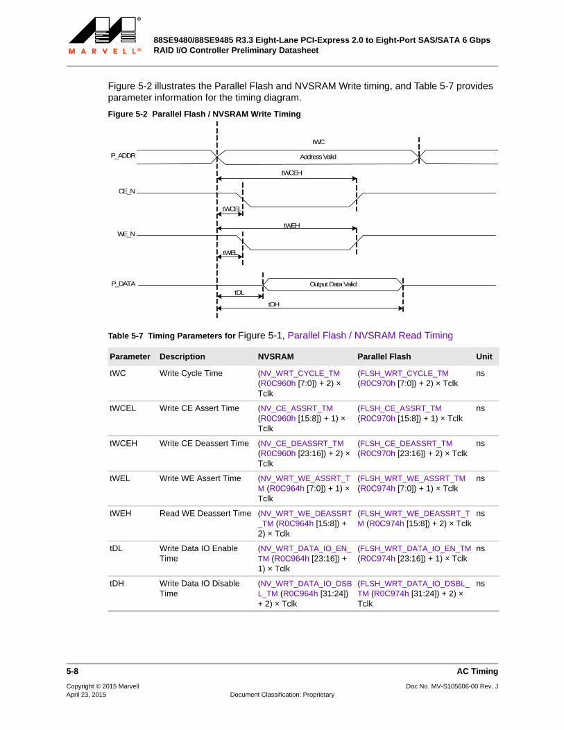
88SE9480/88SE9485 R3.3 Eight-Lane PCI-Express 2.0 to Eight-Port SAS/SATA 6 Gbps RAID I/O Controller Preliminary Datasheet
5-8 AC Timing
Copyright © 2015 Marvell Doc No. MV-S105606-00 Rev. JApril 23, 2015 Document Classification: Proprietary
Figure 5-2 illustrates the Parallel Flash and NVSRAM Write timing, and Table 5-7 provides parameter information for the timing diagram.
Figure 5-2 Parallel Flash / NVSRAM Write Timing
Table 5-7 Timing Parameters for Figure 5-1, Parallel Flash / NVSRAM Read Timing
Parameter Description NVSRAM Parallel Flash Unit
tWC Write Cycle Time (NV_WRT_CYCLE_TM (R0C960h [7:0]) + 2) × Tclk
(FLSH_WRT_CYCLE_TM (R0C970h [7:0]) + 2) × Tclk
ns
tWCEL Write CE Assert Time (NV_CE_ASSRT_TM (R0C960h [15:8]) + 1) × Tclk
(FLSH_CE_ASSRT_TM (R0C970h [15:8]) + 1) × Tclk
ns
tWCEH Write CE Deassert Time (NV_CE_DEASSRT_TM (R0C960h [23:16]) + 2) × Tclk
(FLSH_CE_DEASSRT_TM (R0C970h [23:16]) + 2) × Tclk
ns
tWEL Write WE Assert Time (NV_WRT_WE_ASSRT_TM (R0C964h [7:0]) + 1) × Tclk
(FLSH_WRT_WE_ASSRT_TM (R0C974h [7:0]) + 1) × Tclk
ns
tWEH Read WE Deassert Time (NV_WRT_WE_DEASSRT_TM (R0C964h [15:8]) + 2) × Tclk
(FLSH_WRT_WE_DEASSRT_TM (R0C974h [15:8]) + 2) × Tclk
ns
tDL Write Data IO Enable Time
(NV_WRT_DATA_IO_EN_TM (R0C964h [23:16]) + 1) × Tclk
(FLSH_WRT_DATA_IO_EN_TM (R0C974h [23:16]) + 1) × Tclk
ns
tDH Write Data IO Disable Time
(NV_WRT_DATA_IO_DSBL_TM (R0C964h [31:24]) + 2) × Tclk
(FLSH_WRT_DATA_IO_DSBL_TM (R0C974h [31:24]) + 2) × Tclk
ns
Address Valid
tWC
tWCEH
tWCEL
tWEL
tDH
tWEH
Output Data ValidtDL
P_ADDR
CE_N
WE_N
P_DATA

