magneto-dielectric polymer nanocomposite engineered
TRANSCRIPT
University of South Florida University of South Florida
Scholar Commons Scholar Commons
Graduate Theses and Dissertations Graduate School
2011
Magneto-Dielectric Polymer Nanocomposite Engineered Magneto-Dielectric Polymer Nanocomposite Engineered
Substrate for RF and Microwave Antennas Substrate for RF and Microwave Antennas
Cesar A. Morales University of South Florida, [email protected]
Follow this and additional works at: https://scholarcommons.usf.edu/etd
Part of the American Studies Commons, Electromagnetics and Photonics Commons, and the
Nanoscience and Nanotechnology Commons
Scholar Commons Citation Scholar Commons Citation Morales, Cesar A., "Magneto-Dielectric Polymer Nanocomposite Engineered Substrate for RF and Microwave Antennas" (2011). Graduate Theses and Dissertations. https://scholarcommons.usf.edu/etd/3255
This Dissertation is brought to you for free and open access by the Graduate School at Scholar Commons. It has been accepted for inclusion in Graduate Theses and Dissertations by an authorized administrator of Scholar Commons. For more information, please contact [email protected].
Magneto-Dielectric Polymer Nanocomposite Engineered Substrate for RF and
Microwave Antennas
by
Cesar A. Morales
A dissertation submitted in partial fulfillment of the requirements for the degree of
Doctor of Philosophy Department of Electrical Engineering
College of Engineering University of South Florida
Major Professor: Jing Wang, Ph.D. Thomas M. Weller, Ph.D.
Lawrence Dunleavy, Ph.D. Ryan Toomey, Ph.D.
Hariharan Srikanth, Ph.D.
Date of Approval: October 21, 2011
Keywords: Bandwidth Enhancement, Miniaturization, Nanoparticles, Permeability, Permittivity
Copyright © 2011, Cesar A. Morales

Dedication
To my Wife Paula Algarin, my Mother Cielo Silva, my Father Cesar Morales and
my brothers Julio, Oscar and Andres Morales

Acknowledgements
I like to express my gratitude to my lovely wife, Paula, whom stands by my
side always, supporting me with infinite love and wise words and being my fuel
for everything I have done in the past years.
I would also like to thank my parents Cesar and Cielo. They are my best
counselors and have always been there giving me love and dedication that
helped making me a better person since childhood. They have been my
inspiration and strength that keeps me going on.
I am especially grateful for the moral support received from my brothers,
Julio, Oscar and Andres. They are constantly in my mind and my heart providing
me with the motivation to become a better person.
I want to state my appreciation to my professors Dr. Jing Wang, Dr. Tom
Weller and Dr. Larry Dunleavy for their academic guidance and support in
making me a better scholar and professional in my field.
Finally, special thanks are given to my close friends and colleagues Julio
Dewdney, Daniel Sosa, I-Tsang Wu, Tianpeng Wu, Kosol Son, Sergio Melais,
Julio Medrano, Norma Paz, Michael Konrad, Megan DiTizio, Julie McCoy and
Kristen Stojak. They have always provided me a helping hand during the
moments of need.
i
Table of Contents List of Tables iv List of Figures vi Abstract xiii Chapter 1 - Introduction 1 1.1 Overview 1 1.2 Dissertation Organization 2 1.3 Contributions 3 1.4 Current State of the Art 4 1.4.1 High Losses in Regular Magnetic Substrates 4 1.4.2 Prior Work on Simulation and Modeling of Magneto- Dielectric Materials 7 1.4.3 Issues for the Current State of the Art 9 Chapter 2 - Background and Literature Review 11 2.1 Introduction 11 2.2 Antenna Miniaturization by Using Magneto-Dielectrics 12 2.3 Importance of Substrate in Wave Impedance Matching 13 2.4 Enhancement of the Antenna Bandwidth by Using Magneto- Dielectrics 16 2.5 Simulations of Multilayer Patch Antennas on Dielectric and Magneto-Dielectric Substrates 18 Chapter 3 - Fabrication and Characterization of Magnetite (Fe3O4) Polymer Nanocomposite 24 3.1 Introduction 24 3.2 Setup for Synthesis of Magnetite (Fe3O4) Nanoparticles 25 3.3 Synthesis of Magnetite (Fe3O4) Nanoparticles 26 3.4 Characterization of Magnetite (Fe3O4) Nanoparticles 28 3.4.1 Characterization of Nanoparticles Using X-Ray Diffraction 28 3.4.2 Characterization of Fe3O4 Nanoparticles Using TEM 30 3.5 Preparation and Characterization of PDMS-Fe3O4 Polymer Nanocomposites 35 3.5.1 Characterization of PDMS-Fe3O4 Nanocomposites Using TEM 37
ii
3.5.2 Characterization of the Magnetic Properties of Fe3O4
Nanoparticles Using a Physical Properties Measurement System (PPMS) 39 Chapter 4 - Characterization and Extraction of Complex Permeability and Permittivity of Magnetite-Based Polymer Nanocomposites at Microwave Frequencies 47 4.1 Introduction 47 4.2 Characterization and Extraction of Microwave Properties Using Microstrip Transmission Line Test Fixtures 47 4.2.1 Extraction of the Dielectric/Magnetic Parameters of the Nanocomposite Material Using Multilayer Microstrip Line Test Fixtures 51 4.3 Extracted Dielectric/Magnetic Properties of the PDMS-Fe3O4 Polymer Nanocomposites at Microwave Frequencies 58 4.3.1 Electrical Properties without Applied Magnetic Field 58 4.3.2 Electric Properties of PDMS-Fe3O4 PNCs at 30% w.t. Concentration with External DC Magnetic Biasing Field Applied 61 4.3.3 Electric Properties of PDMS-Fe3O4 PNC at 50% w.t. Concentration with External DC Magnetic Biasing Field Applied 64 4.3.4 Electric Properties of PDMS-Fe3O4 PNC at 80% w.t. Concentration with External DC Magnetic Biasing Field Applied 66 4.4 Magnetic Field Strength Consideration for Optimal Operation of Antennas 69 4.5 Evaluation of the Tunability of Magneto-Dielectric Polymer Nanocomposites Using Microstrip Linear Resonators (MLR) 71 Chapter 5 - Design and Implementation of Multilayer Patch Antennas Using Dielectric and Magneto-Dielectric Nanocomposite Substrates 73 5.1 Introduction 73 5.2 Design of Multilayer Microstrip Antennas 73 5.2.1 First Design: Multilayer Patch Antenna on Plain PDMS Substrate 74 5.2.2 Second Design: Multilayer Patch Antenna on PDMS-Fe3O4 PNC Substrate 78 5.3 Fabrication of Multilayer Microstrip Patch Antennas 80 5.3.1 Fabrication of Multilayer Patch Antennas on PDMS Substrate 81 5.3.2 Multilayer Patch Antenna on Hybrid PDMS/Fe3O4-PDMS Substrate 88 5.4 Experimental Results 91 5.4.1 Pure PDMS-Based Antenna (without Fillers) 91
iii
5.4.2 Multilayer Microstrip Patch Antenna with PDMS-Fe3O4 PNC Filler at 80% w.t. Concentration 95 5.4.3 Multilayer Microstrip Patch Antenna with PDMS-Fe3O4 PNC Filler at 50% w.t. Concentration 98 5.4.4 Multilayer Microstrip Patch Antenna with PDMS-Fe3O4
PNC Filler at 30% w.t. Concentration 101 5.5 Performance Comparison of Multilayer Patch Antennas Built on PDMS-Fe3O4 PNC Substrates with Different Particle Loading Concentrations 104 5.5.1 Performance of PDMS-Fe3O4 PNC Multilayer Antennas without Externally Applied DC Biasing Magnetic Field 104 5.5.2 Performance of PDMS-Fe3O4 PNC Multilayer Antennas with Externally Applied DC Biasing Magnetic Field 112 Chapter 6 – Conclusions and Future Work 126 6.1 Summary and Contributions to the RF/Microwave Field 126 6.2 Recommendation for Future Work and Emerging Projects 127 References 130 About the Author End Page
iv
List of Tables Table 2.1 Relative parameters of the cavity fillers for the microstrip patch antennas 20 Table 2.2 Miniaturization, bandwidth and gain for the microstrip patch antennas using different fillers 23 Table 3.1 Summary of all the peaks in the XRD response for magnetite (Fe3O4) as reported by Hanawalt et al. [19] 29 Table 3.2 Chemical composition of PDMS (Sylgard 184, Dow Corning) base resin 35 Table 3.3 Chemical composition of PDMS (Sylgard 184, Dow Corning) curing agent 35 Table 3.4 Electrical properties of PDMS (Sylgard 184, Dow Corning) when a 10:1 mixing ratio of base resin to curing agent is applied 36 Table 3.5 Blocking temperatures and saturation magnetization for the Fe3O4 nanoparticles and PDMS-Fe3O4 PNCs 46 Table 4.1 TRL calibration standards on Rogers RT/Duroid 6010LM 50 Table 5.1 Antenna parameters of plain PDMS-based substrate design 93 Table 5.2 Antenna parameters for the PDMS-Fe3O4 PNC 80% w.t. substrate design 98 Table 5.3 Antenna parameters for the PDMS-Fe3O4 PNC 50% w.t. substrate design 101 Table 5.4 Antenna parameters for the PDMS-Fe3O4 PNC 30% w.t. substrate design 104 Table 5.5 Multilayer patch antennas and their relevant properties without any applied biasing magnetic field 111
v
Table 5.6 Electrical properties of PNC substrates without any applied DC biasing magnetic field 112 Table 5.7 Antenna parameters of PDMS-Fe3O4 PNC 80% w.t. substrate
design with and without applied external DC biasing magnetic field 118 Table 5.8 Antenna parameters of all the multilayer patch antennas with PNC-filled substrates and applied external DC biasing magnetic field 124 Table 5.9 Field susceptibility of the antenna performance parameters, for all the multilayer patch antennas with PNC-filled substrates, to external DC biasing magnetic field 125
vi
List of Figures Figure 1.1 (a) Six-inch wire dipole antenna over a finite matched impedance layer (MIL); (b) Six-inch circular dipole over a finite MIL on a PEC (Perfect Electric Conductor) surface 5 Figure 1.2 Measured boresight gain for (a) the wire dipole shown in Figure 1.1 (a); and (b) the circular dipole shown in Figure 1.1 (b) 6 Figure 1.3 Exploded and collapsed-view schematics of the stacked-patch antenna design using magneto-dielectric substrates 7 Figure 1.4 Antenna miniaturization factor vs. the broadside gain at the center frequency obtained for several designs 8 Figure 2.1 Wave reflection and transmission across the substrate and free space interface 14 Figure 2.2 Theoretical BW and |b| vs. r while a patch antenna retains the same dimensions 17 Figure 2.3 (a) 3D perspective-view schematic of the multi-layer microstrip patch antenna; (b) Top view layout of the antenna 19 Figure 2.4 Simulated return loss (dB) vs. frequency for the microstrip patch antennas, using dielectric-only and magneto-dielectric substrate fillers 21 Figure 2.5 Simulated broadside gain (dB) vs. frequency for the microstrip patch antennas, using dielectric-only and magneto-dielectric substrate fillers 22 Figure 3.1 Simplified diagram that illustrates the formation of Fe3O4 nanoparticles 27 Figure 3.2 X-Ray diffraction pattern of as-synthesized magnetite (Fe3O4) nanoparticles 30
vii
Figure 3.3 Transmission Electron Microscopy (TEM) of Fe3O4 nanoparticles with mean size 7.53 nm 31 Figure 3.4 High resolution (TEM) image of as-synthesized magnetite (Fe3O4) nanoparticles 33 Figure 3.5 Magnified high resolution (TEM) image of as-synthesized Fe3O4 nanoparticles, revealing the co-existence of different crystal orientation planes 34 Figure 3.6 TEM image of Fe3O4-PDMS polymer nanocomposite at relatively low particle loading concentration 38 Figure 3.7 High resolution (TEM) image of Fe3O4-PDMS polymer nanocomposite with high particle loading concentration 38 Figure 3.8 Magnetization curves for as-synthesized magnetite (Fe3O4) nanoparticles and the PDMS-Fe3O4 polymer nanocomposites at different concentrations (30%, 50% and 80% w.t.) 39 Figure 3.9 Field Cooled (FC) and Zero-Field Cooled (ZFC) curves under 200Oe of applied magnetic field for plain Fe3O4 nanoparticles 42 Figure 3.10 Field Cooled (FC) and Zero-Field Cooled (ZFC) curves at 200Oe for PDMS-Fe3O4 polymer nanocomposites at 30% w.t. concentration 43 Figure 3.11 Field Cooled (FC) and Zero-Field Cooled (ZFC) curves at 200Oe for PDMS-Fe3O4 polymer nanocomposites at 50% w.t. concentration 43 Figure 3.12 Field Cooled (FC) and Zero-Field Cooled (ZFC) curves at 200Oe for PDMS-Fe3O4 polymer nanocomposites at 80% w.t. concentration 44 Figure 3.13 Comparison of the FC and ZFC curves at 200Oe for plain Fe3O4 and PDMS-Fe3O4 polymer nanocomposites with particle loading concentrations of 30% w.t., 50% w.t. and 80% w.t., respectively 45 Figure 4.1 Schematic of two-port microwave test setup with fixed electromagnet 48 Figure 4.2 3D perspective-view schematic of the multilayer microstrip test fixture for extraction of the microwave properties of the magneto-dielectric polymer nanocomposites 49
viii
Figure 4.3 Schematic diagram of the measurement fixture 52 Figure 4.4 Cross-sectional diagram of the multilayer microstrip 55 Figure 4.5 Flux diagram for the iterative calculations of r and r 57 Figure 4.6 Extracted permittivity for PDMS and magneto-dielectric PNCs without applied magnetic field 58 Figure 4.7 Extracted permeability for PDMS and magneto-dielectric PNCs without applied magnetic field 59 Figure 4.8 Extracted dielectric loss tangent for PDMS and magneto-dielectric PNCs without applied magnetic field 60 Figure 4.9 Extracted magnetic loss tangent for PDMS and magneto-dielectric PNCs without applied magnetic field 61 Figure 4.10 3D plot (left) of the complete extracted relative permittivity vs. magnetic field for PDMS-Fe3O4 PNC at 30% w.t. concentration 62 Figure 4.11 3D plot (left) of the complete extracted relative permeability vs. magnetic field for PDMS-Fe3O4 PNC at 30% w.t. concentration 62 Figure 4.12 3D plot (left) of the complete extracted dielectric loss tangent vs. magnetic field for PDMS-Fe3O4 PNC at 30% w.t. concentration 63 Figure 4.13 3D plot (left) of the complete extracted magnetic loss tangent vs. magnetic field for PDMS-Fe3O4 PNC at 30% w.t. concentration 63 Figure 4.14 3D plot (left) of the complete extracted relative permittivity vs. magnetic field for PDMS-Fe3O4 PNC at 50% w.t. concentration 64 Figure 4.15 3D plot (left) of the complete extracted relative permeability vs. magnetic field for PDMS-Fe3O4 PNC at 50% w.t. concentration 65 Figure 4.16 3D plot (left) of the complete extracted dielectric loss tangent vs. magnetic field for PDMS-Fe3O4 PNC at 50% w.t. concentration 65
ix
Figure 4.17 3D plot (left) of the complete extracted magnetic loss tangent vs. magnetic field for PDMS-Fe3O4 PNC at 50% w.t. concentration 66 Figure 4.18 3D plot (left) of the complete extracted relative permittivity vs. magnetic field for PDMS-Fe3O4 PNC at 80% w.t. concentration 67 Figure 4.19 3D plot (left) of the complete extracted relative permeability vs. magnetic field for PDMS-Fe3O4 PNC at 80% w.t. concentration 67 Figure 4.20 3D plot (left) of the complete extracted dielectric loss tangent vs. magnetic field for PDMS-Fe3O4 PNC at 80% w.t. concentration 68 Figure 4.21 3D plot (left) of the complete extracted magnetic loss tangent vs. magnetic field for PDMS-Fe3O4 PNC at 80% w.t. concentration 68 Figure 4.22 Optimal conditions for miniaturization and impedance matching of the antenna with the surroundings (magneto-dielectric condition) 70 Figure 4.23 Measured transmission characteristics (S21) of the MLR with embedded polymer nanocomposites 72 Figure 4.24 Measured Q-factor and resonant frequency versus DC magnetic field strength 72 Figure 5.1 3D schematic diagram of the multilayer microstrip patch antenna identifying all its layers and their thicknesses 75 Figure 5.2 A perspective-view (left) and top-view (right) schematic of the assembled multilayer antenna identifying key features and dimension parameters 76 Figure 5.3 Simulated return loss for a Rogers 3850/PDMS/Rogers 3850 multilayer patch antenna 77 Figure 5.4 3D schematic of the multilayer microstrip patch antenna with a cavity embedded completely filled with PDMS-Fe3O4 PNC 79
x
Figure 5.5 A perspective-view (left) and top-view (right) schematic of the assembled multilayer antenna, which includes a PDMS-Fe3O4 PNC filled cavity underneath the antenna patch 79 Figure 5.6 Simulated return loss for the multilayer patch antenna with embedded PDMS-Fe3O4 nanocomposite and 80% w.t. loading 80 Figure 5.7 Cross-sectional view diagram of the fabrication process flow for patterning the ground plane on one side of a Rogers LCP 3850 laminate 82 Figure 5.8 Cross-sectional view diagram of the fabrication process flow for definition of the antenna patch on one side of a Rogers LCP 3850 laminate 83 Figure 5.9 Perspective-view schematic diagram for the step-by-step process flow of the PDMS based multilayer antenna 86 Figure 5.10 Pictures of the multilayer patch antenna on a molded PDMS substrate using the process flow shown in Figure 5.9 87 Figure 5.11 Diagram with the different steps in the construction of the PDMS-Fe3O4 PNC based multilayer antenna 89 Figure 5.12 Top-view photo of multilayer patch antenna constructed on PDMS-Fe3O4 PNC substrate following the process flow described in Figure 5.11 90 Figure 5.13 Measured and simulated return loss for the patch antenna on pure PDMS-based molded multilayer substrate, showing acceptable agreement in resonance frequencies 92 Figure 5.14 Measured and simulated E-Plane radiation pattern for the patch antenna on molded PDMS-based multilayer substrate 92 Figure 5.15 Measured and simulated H-Plane radiation pattern for the patch antenna on molded PDMS-based multilayer substrate 93 Figure 5.16 Measured gain vs. frequency for the multilayer patch antenna on molded PDMS-based substrate 94 Figure 5.17 Return loss for the microstrip multilayer patch antenna with PDMS-Fe3O4 PNC at 80% w.t. 95
xi
Figure 5.18 Measured and simulated E-Plane radiation pattern for the multilayer patch antenna on 80% w.t. PDMS-Fe3O4 PNC-based substrate 96 Figure 5.19 Measured and simulated H-Plane radiation pattern for the multilayer patch antenna on 80% w.t. PDMS-Fe3O4 PNC-based substrate 97 Figure 5.20 Return loss for the microstrip multilayer antenna with PDMS-Fe3O4 PNC at 50% w.t. 98 Figure 5.21 Measured and simulated E-Plane radiation pattern for the multilayer patch antenna on 50% w.t. PDMS-Fe3O4 PNC-based substrate 99 Figure 5.22 Measured and simulated H-Plane radiation pattern for the multilayer patch antenna on 50% w.t. PDMS-Fe3O4 PNC-based substrate 100 Figure 5.23 Return loss for the microstrip multilayer antenna with PDMS-Fe3O4 PNC at 30% w.t. 101 Figure 5.24 Measured and simulated E-Plane radiation pattern for the multilayer patch antenna on 30% w.t. PDMS-Fe3O4 PNC-based substrate 102 Figure 5.25 Measured and simulated H-Plane radiation pattern for the multilayer patch antenna on 30% w.t. PDMS-Fe3O4 PNC-based substrate 103 Figure 5.26 Measured return losses for plain PDMS and 80% w.t. PDMS-Fe3O4 PNC multilayer patch antennas 105 Figure 5.27 Top-view photo of plain PDMS (left) and 80% w.t. PDMS-Fe3O4 PNC (right) multilayer patch antennas 106 Figure 5.28 Measured return losses of PDMS-Fe3O4 PNC multilayer patch antennas at 30%, 50% and 80% w.t. concentrations 107 Figure 5.29 Measured gain of PDMS-Fe3O4 PNC multilayer patch antennas at 30%, 50% and 80% w.t. concentrations 110 Figure 5.30 Neodymium magnet array placed in contact with a PDMS-Fe3O4 PNC multilayer antenna 114
xii
Figure 5.31 Measured return loss of the PDMS-Fe3O4 PNC multilayer patch antenna at 80% w.t. concentration with and without externally applied DC magnetic field 115 Figure 5.32 Measured gain of PDMS-Fe3O4 PNC multilayer patch antenna at 80% w.t. concentration with and without DC biasing magnetic field 116 Figure 5.33 Measured E-Plane radiation pattern of PDMS-Fe3O4 PNC multilayer patch antenna at 80% w.t concentration with and without applied DC biasing magnetic field 117 Figure 5.34 Measured return loss of PDMS-Fe3O4 PNC multilayer patch antenna at 50% w.t. concentration with and without applied magnetic field 118 Figure 5.35 Measured E-Plane radiation pattern of PDMS-Fe3O4 PNC multilayer patch antenna at 50% w.t. concentration with and without applied magnetic field 119 Figure 5.36 Measured gain of PDMS-Fe3O4 PNC multilayer patch antenna at 50% w.t. concentration with and without applied DC biasing magnetic field 120 Figure 5.37 Measured return loss of PDMS-Fe3O4 PNC multilayer patch antenna at 30% w.t. concentration with and without applied DC biasing magnetic field 121 Figure 5.38 Measured E-Plane radiation pattern of PDMS-Fe3O4 PNC multilayer patch antenna at 30% w.t. concentration with and without applied magnetic field 122 Figure 5.39 Measured gain of PDMS-Fe3O4 PNC multilayer patch antenna at 30% w.t. concentration with and without applied magnetic field 123
xiii
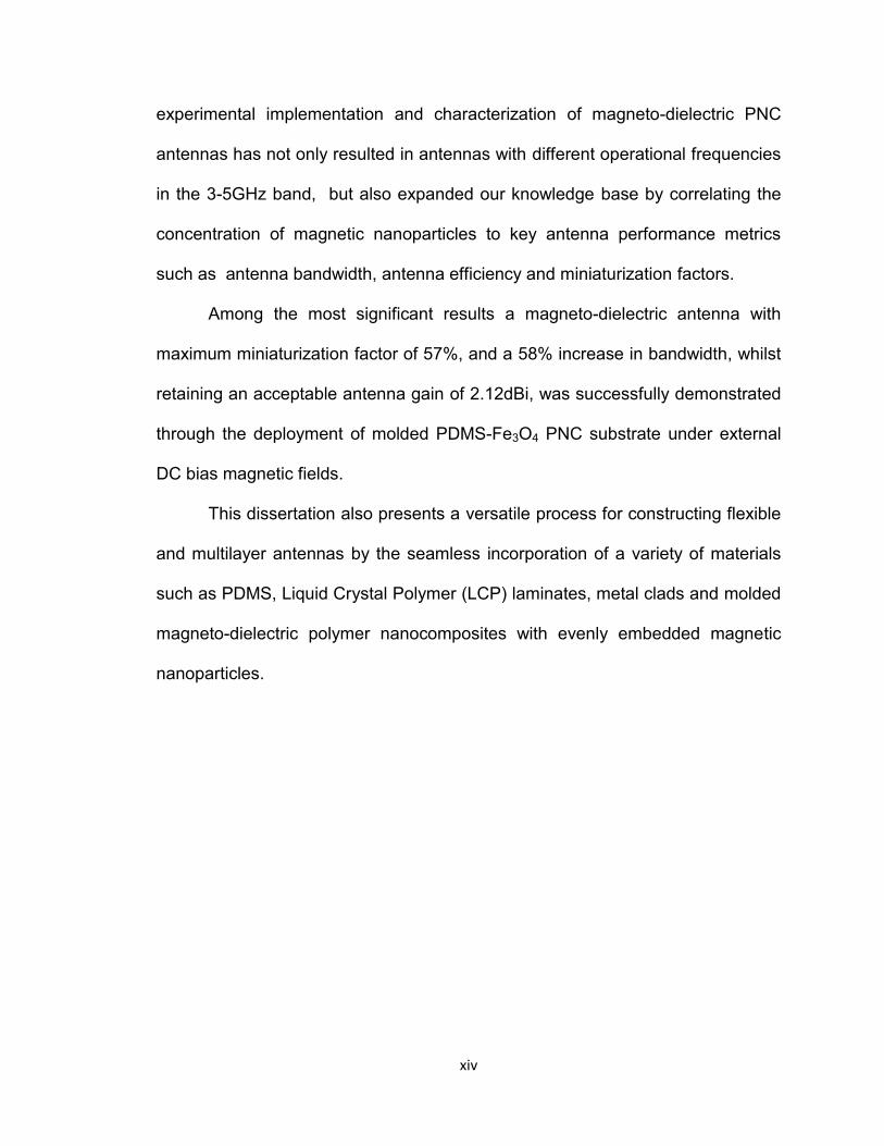
Abstract
This dissertation presents the first reported systematic investigation on the
implementation of multilayer patch antennas over Fe3O4–based polymer
nanocomposite (PNC) magneto-dielectric substrates. The PNC substrate is
created by the monodispersion of Fe3O4 nanoparticles, with mean size of 7.5nm,
in a polymeric matrix of Polydimethylsiloxane (PDMS).
Recently, magneto-dielectric substrates have been proposed by several
researchers as a means for decreasing the size and increasing the bandwidth of
planar antennas. Nevertheless, factors such as high loss and diminished control
over magnetic and dielectric properties have hindered the optimal performance of
antennas. In addition, the incompatibility and elevated complexity prevents
integration of conventional magnetic materials with antennas and standard
fabrication processes at printed circuit boards (PCBs) and wafer levels.
Additionally, the low hysteresis losses exhibited by uniformly embedded
superparamagnetic nanoparticles complemented by the ease of integration of
polymer nanocomposites in standard fabrication processes, offer promising
solutions to resolve any of the complications and concerns foresaid.
Towards this dissertation work, one multilayer antenna was constructed
over a molded PDMS substrate along with three similar antennas built on PDMS-
Fe3O4 PNC substrates with different Fe3O4 nanoparticle loading concentrations in
the PDMS matrix of 80%, 50% and 30% by weight. This pioneering work in the
xiv
experimental implementation and characterization of magneto-dielectric PNC
antennas has not only resulted in antennas with different operational frequencies
in the 3-5GHz band, but also expanded our knowledge base by correlating the
concentration of magnetic nanoparticles to key antenna performance metrics
such as antenna bandwidth, antenna efficiency and miniaturization factors.
Among the most significant results a magneto-dielectric antenna with
maximum miniaturization factor of 57%, and a 58% increase in bandwidth, whilst
retaining an acceptable antenna gain of 2.12dBi, was successfully demonstrated
through the deployment of molded PDMS-Fe3O4 PNC substrate under external
DC bias magnetic fields.
This dissertation also presents a versatile process for constructing flexible
and multilayer antennas by the seamless incorporation of a variety of materials
such as PDMS, Liquid Crystal Polymer (LCP) laminates, metal clads and molded
magneto-dielectric polymer nanocomposites with evenly embedded magnetic
nanoparticles.
1
Chapter 1
Introduction
1.1 Overview
The work presented in this dissertation introduces the implementation of
bandwidth-enhanced patch antennas on molded magneto-dielectric polymer
nanocomposite substrates, which are the first of their kind. A patch antenna
design is selected because of its high susceptibility to the substrate
characteristics. This antenna has a microstrip configuration, and therefore the
field interaction between the patch and the ground plane largely occurs in the
substrate underneath the patch. Taking advantage of this condition, the patch is
placed over a cavity filled with magneto-dielectric nanocomposite material. In
particular, polymer nanocomposites consisting of Magnetite (Fe3O4)
nanoparticles, evenly dispersed in a Polydimethylsiloxane (PDMS) matrix, are
prepared in order to fill the cavity. The unique magneto-dielectric properties of
this engineered material facilitate the miniaturization of the antenna, while
improving its performance by widening the antenna bandwidth as compared to
those of conventional counterparts designed on pure dielectric substrates, and
improving impedance matching to free-space (i.e., air around the antenna). The
implementation of magneto-dielectric substrate opens the possibility of
miniaturization using new materials while retaining low permittivity, which
reduces energy trapping inside the substrate, and thus facilitating the radiation of
2
the antenna to free space. The decreased permittivity also helps mitigate losses
caused by the excitation of surfaces waves into the substrate.
The complex permittivity and permeability of the magnetite polymer
nanocomposites are both sensitive to external DC bias magnetic fields, thereby
enabling optional tuning of the operational frequency and the modification of the
antenna radiation characteristics (i.e. antenna efficiency)
1.2 Dissertation Organization
This dissertation is organized into six chapters, with the first and sixth
corresponding to introduction and conclusions respectively. Chapters two
through five describe the primary contributions of the work developed in this
dissertation.
Chapter 2 presents the background and review of magneto-dielectric
substrates for antenna implementation and development. There, the basics on
the electrical properties of dielectric and magnetic materials are presented,
providing a detailed description of complex permeability and permittivity.
Thereafter, an overview on how the properties of the material define antenna size
and performance is elaborated. Finally, electromagnetic simulations are used to
demonstrate the advantages of using magneto-dielectric versus pure dielectric
substrates.
Chapter 3 presents the fabrication and characterization of magnetite
(Fe3O4) polymer nanocomposites. Initially, a brief explanation of the
characteristics of magnetite nanoparticles is provided. Thereafter, synthesis and
characterization of nanoparticles and polymer nanocomposites are described.
3
Chapter 4 presents the methodology for characterization and extraction of
complex permeability and permittivity of polymer nanocomposites using
microstrip transmission line test fixtures. This chapter explains in detail how well-
known techniques, such as the Nicolson-Ross-Weir and Barker Jarvis methods
were adapted for multilayer microstrip-based structures for the purpose of
extracting the electrical properties of magneto-dielectric materials.
Chapter 5 presents the design and implementation of multilayer patch
antennas equipped with dielectric and magneto-dielectric substrates.
Experimental results are presented to reveal the substantial influence of the
electrical properties of the material (i.e. permeability, permittivity, dielectric and
magnetic loss tangents) on the overall performance of the magneto-dielectric
antennas.
1.3 Contributions
The main contribution from this dissertation work is the implementation of
magneto-dielectric polymer nanocomposites for the miniaturization and
bandwidth enhancement of microstrip patch antennas, while upholding
acceptable performance as well as functional radiation characteristics.
Deployment of newly developed polymer nanocomposites in
RF/microwave antennas, calls for the extraction of the intrinsic electrical
properties of these materials, which is deemed essential for the effective design
and implementation of such devices. This process was developed by engineering
a hybrid algorithm that combines time-domain techniques [23], frequency domain
4
techniques [22][26], with transmission line theory and conformal mapping
methods [24][25][27]-[35].
A multilayer patch antenna design has been developed here to
demonstrate the usefulness of magneto-dielectric nanocomposites, easiness in
the processing and integration techniques onto PCB level design, and their
soaring potentiality of integration to micro-fabrication levels.
Magneto-dielectric polymer nanocomposites have been systematically
studied by implementing different concentrations of magnetite (Fe3O4)
nanoparticles (80%, 50% and 30% by weight) in a polymeric matrix of
Polydimethylsiloxane (PDMS) and the trade-offs between miniaturization,
bandwidth enhancement, antenna performance and concentration of
nanoparticles have been successfully identified.
1.4 Current State of the Art
The most common practice for antenna miniaturization has traditionally
rested in using high permittivity substrates for the purpose of reducing the
antenna size by a factor roughly proportional to √ . However, size reduction is
achieved at the expense of lowering the antenna gain and bandwidth, which is
caused by the excessive coupling between the patch and ground plane. In
addition, high permittivity materials tend to be heavy (e.g., ceramics) hence not
viable for lightweight antenna structures [1].
1.4.1 High Losses in Regular Magnetic Substrates
As an alternative approach, several antennas incorporating magneto-
dielectric substrates have been presented, which continue to cope with issues
5
related with high material losses [2]. This is particularly the case of an antenna
configuration recently proposed by Erkmen at al., in which ferrite layers with
magnetic loss and dielectric loss tangents of around 0.2 (tand tanm 0.2) are
implemented [3]. The effect of material losses has been decreased by
maintaining a given distance between the printed antenna and the magneto-
dielectric layer, with some drawbacks related to a high profile (above 2 inches)
[2]. Undoubtedly, some important enhancements in the antenna radiation field
have been achieved using the ground plane as a reflector, even at frequencies
when the distance between the antenna and the ground plane becomes less
than /20 [2]. It is here that the trade-off between the overall antenna height,
weight and performance becomes a matter of important interest.
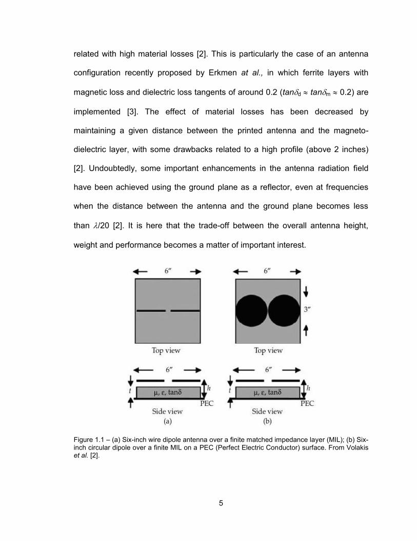
Figure 1.1 – (a) Six-inch wire dipole antenna over a finite matched impedance layer (MIL); (b) Six-inch circular dipole over a finite MIL on a PEC (Perfect Electric Conductor) surface. From Volakis et al. [2].
6
Two typical antenna configurations on a ferrite-coated ground plane are
shown in Figure 1.1 These designs are based on the strategic selection of
materials and configurations that lead to a suppressed destructive interference
caused by the ground plane, and consequently resulting in larger antenna gain
compared to a free standing antenna [2].
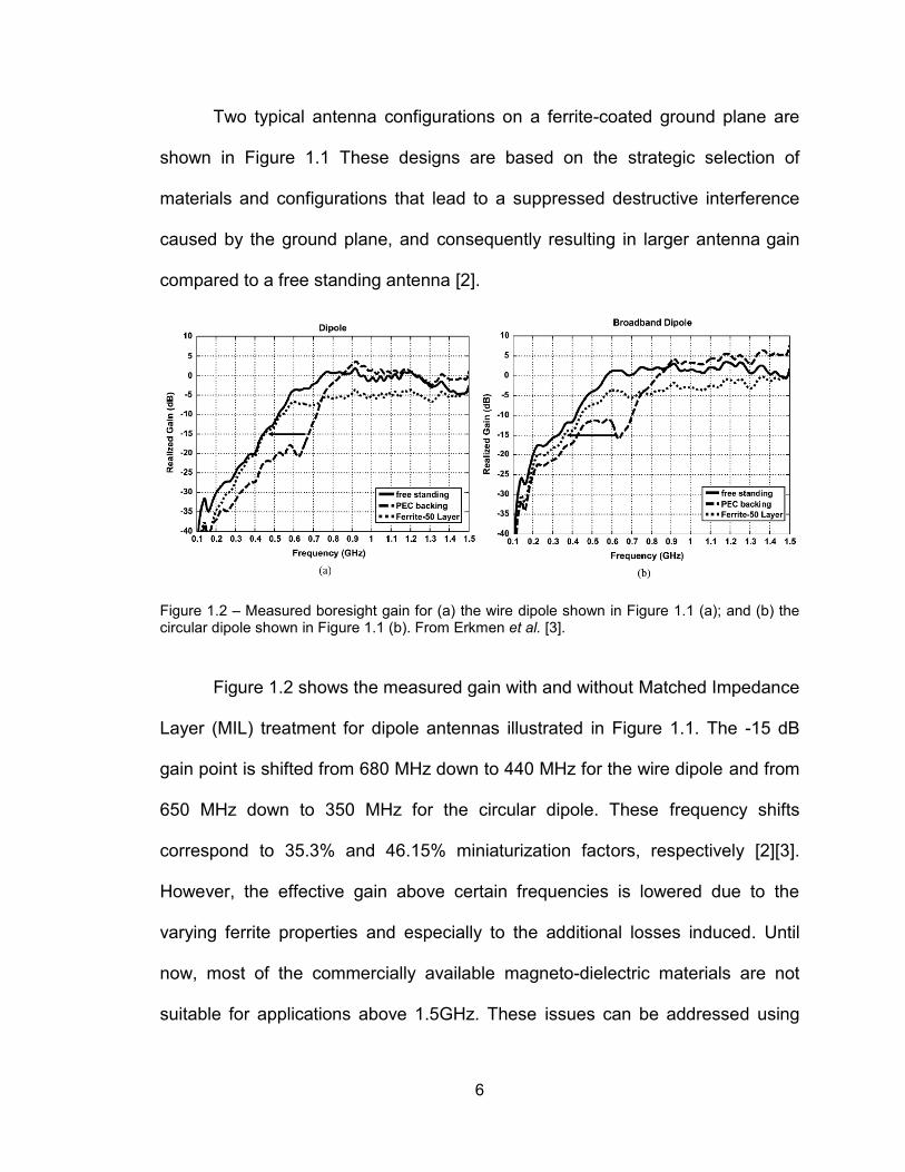
Figure 1.2 – Measured boresight gain for (a) the wire dipole shown in Figure 1.1 (a); and (b) the circular dipole shown in Figure 1.1 (b). From Erkmen et al. [3].
Figure 1.2 shows the measured gain with and without Matched Impedance
Layer (MIL) treatment for dipole antennas illustrated in Figure 1.1. The -15 dB
gain point is shifted from 680 MHz down to 440 MHz for the wire dipole and from
650 MHz down to 350 MHz for the circular dipole. These frequency shifts
correspond to 35.3% and 46.15% miniaturization factors, respectively [2][3].
However, the effective gain above certain frequencies is lowered due to the
varying ferrite properties and especially to the additional losses induced. Until
now, most of the commercially available magneto-dielectric materials are not
suitable for applications above 1.5GHz. These issues can be addressed using
7
more complex geometries and configurations, such as tapered lines or selective
variations in the thickness of the coated MIL layer [1].
1.4.2 Prior Work on Simulation and Modeling of Magneto-Dielectric Materials
Namin et al. [1] have proposed a methodology to design stacked-patch
antennas based on magneto-dielectric substrates. In particular, they created an
antenna in which the effective permeability and permittivity holds the same value,
which is also referred as the matched magneto-dielectric condition. Under this
circumstance, the impedance of the antenna is going to be equal to that of the
free space. This unique property allows for a better impedance matching over the
bandwidth of the antenna, thus decreasing any losses due to wave reflection
within the antenna and the free space. Additionally, even with moderated values
of permeability and permittivity of less than 5, considerable reductions in length,
width and thickness were achieved [1].
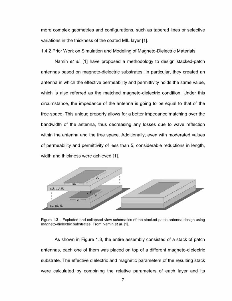
Figure 1.3 – Exploded and collapsed-view schematics of the stacked-patch antenna design using magneto-dielectric substrates. From Namin et al. [1].
As shown in Figure 1.3, the entire assembly consisted of a stack of patch
antennas, each one of them was placed on top of a different magneto-dielectric
substrate. The effective dielectric and magnetic parameters of the resulting stack
were calculated by combining the relative parameters of each layer and its
8
intervening volumetric fractions. The antenna was strategically designed using a
genetic algorithm (GA), where its overall size and broadside gain were
considered as the target parameters while keeping the matched magneto-
dielectric condition [1]. To maintain this condition, unwarranted adjustments were
adopted, such as the dynamic assignation of values for the effective parameters
of each individual substrate layer.
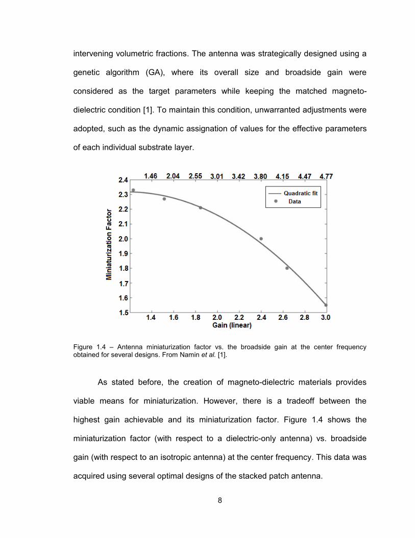
Figure 1.4 – Antenna miniaturization factor vs. the broadside gain at the center frequency obtained for several designs. From Namin et al. [1].
As stated before, the creation of magneto-dielectric materials provides
viable means for miniaturization. However, there is a tradeoff between the
highest gain achievable and its miniaturization factor. Figure 1.4 shows the
miniaturization factor (with respect to a dielectric-only antenna) vs. broadside
gain (with respect to an isotropic antenna) at the center frequency. This data was
acquired using several optimal designs of the stacked patch antenna.
9
Miniaturization of antenna typically leads to some level of performance
degradation that cannot be avoided, even with the use of magneto dielectric
materials. The performance of the antenna is going to suffer due to the reduction
of its physical area and the increment of confined energy given the proximity of
the metallization layers. In addition, the results presented in [1] are based in
simulations under ideal circumstances, with the loss properties of the magneto-
dielectric materials and the metallization layers being neglected. Undoubtedly,
the aforementioned loss related properties would introduce a negative impact on
the overall performance of any antenna implemented in real applications.
Another proposed approach was to employ thin ferromagnetic layers
based on metals such as iron and cobalt [4]. However, this type of laminate may
be used only at frequencies below 2-3GHz, because the effective permeability
drops rapidly while frequency is increased. These materials also exhibit higher
magnetic losses at high frequencies [4].
1.4.3 Issues for the Current State of the Art
As explained previously, high permittivity materials are frequently used for
antenna miniaturization at the expense of reduced gain and bandwidth, resulting
from incremented capacitive coupling throughout the substrate.
Despite the fact that magneto-dielectric materials present a promising new
approach for miniaturization of components, the currently available magneto-
dielectric materials exhibit high losses that adversely affect the performance of
current antenna designs. Moreover, commercially available materials are not well
suited for device applications above 1.5GHz [2]. Permittivity and permeability

10
both tend to decrease as the operational frequency is increased. The presence of
ferromagnetic resonances and high loss properties have curtailed wider
acceptance of magneto-dielectric materials usage for implementing antennas at
higher frequencies.
Commercially available magnetic materials are generally non-versatile.
High permeability materials are often hard and heavy (e.g. Iron, cobalt and other
ferrites) and therefore unsuitable for the fabrication of lightweight antennas.
Moreover, it is difficult to integrate these materials through conventional
fabrication processes especially when physical flexibility is greatly preferred. This
dissertation work represents one of the first attempts to fill this knowledge and
technology gap.
11
Chapter 2
Background and Literature Review
2.1 Introduction
Materials used for RF and microwave antennas are selected based on
their effective electrical properties. In recent years, electromagnetic properties
such as complex permeability and permittivity offered by engineered
metamaterials have shown great promise in the miniaturization of antennas.
Nevertheless, the size reductions yielded by these metamaterials that consist of
periodic structures, are still burdened by the undesired performance issue of
narrow bandwidth. Nowadays, researchers have been interested in carefully
exploring intrinsic details of the materials, with the specific goal of tailoring their
dielectric and magnetic properties, and thus granting improvements in the
performance of RF/microwave devices (e.g. antennas). Particularly, magneto-
dielectric materials have been widely examined for antenna applications,
exhibiting excellent advantages amid several unresolved deficiencies. Aside from
the fact that permittivity and permeability diminish as the operational frequency
increases, high dielectric and magnetic losses and incompatibility with standard
fabrication processes are some of the other challenges that still require
resolution. These setbacks are addressed in following chapters, in which
magneto-dielectric nanocomposites are proposed as a favorable alternative to
miniaturizing and improving the performance of microstrip antennas.
12
Also presented in this chapter is a review on the fundamental antenna
design concepts related to the implementation of magneto-dielectric materials as
the engineered substrate. A comprehensive overview of the electrical properties
of such materials is shown to explain how the presence of complementary
magnetic and dielectric properties is advantageous to enhancing the general
performance of planar antennas. In the chosen rectangular microstrip patch
antenna topology, the field distribution is confined inside the substrate, between
the patch and the ground plane. Consequently, the electrical properties of the
substrate determine the overall performance of such a device, thereby setting the
performance metrics to include the bandwidth, size and efficiency of the antenna.
Finally, patch antennas are designed and simulated using a variety of engineered
substrates (from pure dielectric to magneto-dielectric materials). Comparisons of
the different designs provide a good understanding of how the performance of
the antenna is characteristically defined by the electrical properties of the
substrate.
2.2 Antenna Miniaturization by Using Magneto-Dielectrics
Miniaturization, bandwidth enhancement and impedance matching to its
surrounding media have become the major concerns for antenna designers. One
of the biggest issues for the employment of materials with high permittivity is that
the improvement in miniaturization factor results in reduced bandwidth and
inferior impedance matching. The key challenges and tradeoffs between the
aforementioned performance metrics as well as their dependency on the
13
electrical properties of the substrate are relatively understood by classical
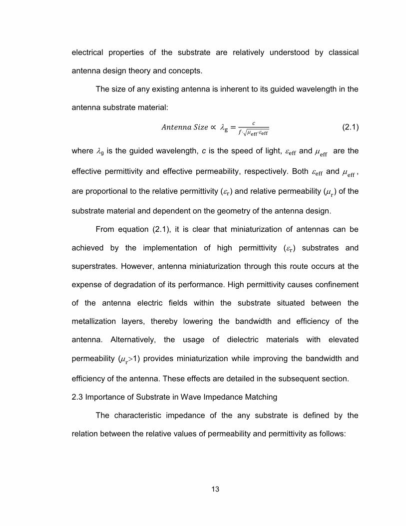
antenna design theory and concepts.
The size of any existing antenna is inherent to its guided wavelength in the
antenna substrate material:
√ (2.1)
where g is the guided wavelength, c is the speed of light, and
are the
effective permittivity and effective permeability, respectively. Both and
,
are proportional to the relative permittivity ( ) and relative permeability ( ) of the
substrate material and dependent on the geometry of the antenna design.
From equation (2.1), it is clear that miniaturization of antennas can be
achieved by the implementation of high permittivity ( ) substrates and
superstrates. However, antenna miniaturization through this route occurs at the
expense of degradation of its performance. High permittivity causes confinement
of the antenna electric fields within the substrate situated between the
metallization layers, thereby lowering the bandwidth and efficiency of the
antenna. Alternatively, the usage of dielectric materials with elevated
permeability ( 1) provides miniaturization while improving the bandwidth and
efficiency of the antenna. These effects are detailed in the subsequent section.
2.3 Importance of Substrate in Wave Impedance Matching
The characteristic impedance of the any substrate is defined by the
relation between the relative values of permeability and permittivity as follows:
14
√
⁄ √
⁄ √
⁄ (2.2)
where is the characteristic impedance of the free space.
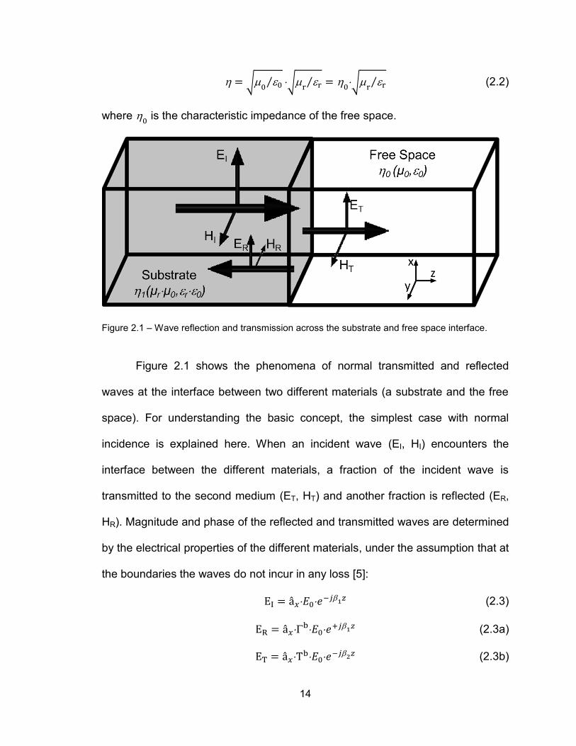
Figure 2.1 – Wave reflection and transmission across the substrate and free space interface.
Figure 2.1 shows the phenomena of normal transmitted and reflected
waves at the interface between two different materials (a substrate and the free
space). For understanding the basic concept, the simplest case with normal
incidence is explained here. When an incident wave (EI, HI) encounters the
interface between the different materials, a fraction of the incident wave is
transmitted to the second medium (ET, HT) and another fraction is reflected (ER,
HR). Magnitude and phase of the reflected and transmitted waves are determined
by the electrical properties of the different materials, under the assumption that at
the boundaries the waves do not incur in any loss [5]:
(2.3)
(2.3a)
(2.3b)
15
(2.3c)
(2.3d)
(2.3e)
where is the amplitude of the incident electric field, is the characteristic
impedance of the substrate, is the characteristic impedance of the free space,
is the phase constant of the substrate,
is the phase constant of the free
space, and represent the reflection and transmission coefficient at the
interface, respectively.
and can be calculated directly from the characteristic impedances of
the two different materials[5]:
(2.4)
(2.5)
As observed in Equation (2.2), the characteristic impedance of high
permittivity substrate is significantly low, posing a challenge against matching of
the antenna substrate with the surrounding environment. From Equations (2.4)
and (2.5) the optimum impedance matching is obtained when =
, which
implies zero reflection ( =0). From equation (2.2), this condition is readily
achievable when the substrate is made of a magneto-dielectric material with
equivalent relative permittivity and permeability = .

16
2.4 Enhancement of the Antenna Bandwidth by Using Magneto-Dielectrics
The antenna bandwidth is also affected by the electrical properties of the
substrate. Hansen and Burke derived a good approximation for the calculation of
the bandwidth, based on a combination of the cavity and transmission line
models for rectangular patch antennas, in which the resultant bandwidth is
mainly controlled by the radiation resistance by assuming a substrate material
with low loss properties [6]. For values of 1, a good approximation for the
radiation conductance is given by [6]:
√ (2.6)
The characteristic admittance of a wide microstrip line is given by [7]:
√
√
(2.7)
where is the line width (patch width) and is the substrate thickness. Based on
the zero-order theory, the following expression is inherent to a resonant patch:
√ (2.8)
Furthermore, from equations (2.7) and (2.8), the characteristic admittance of the
patch can be expressed as:
(2.9)
The quality factor can be then expressed in terms of the radiation
conductance and the characteristic admittance [7]:
(2.10)
The zero-order bandwidth BW can be defined at a VSWR2 as [6]:
17
√ (2.11)
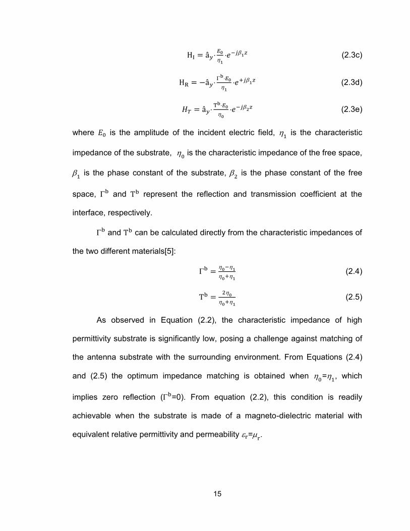
Finally, combining Equations (2.6), (2.9), (2.10) and (2.11) [6]:
√
√ [ √ ] (2.12)
where is the free space wavelength.
Assuming a patch antenna with substrate thickness =1.57mm and zero-
order resonance at 4GHz ( =74.95mm), equation (2.12) can be evaluated by
assigning different values to and . BW is evaluated for 1<
<5 while keeping
a constant . In this case, theoretically, resonance frequency will remain
constant if the antenna dimensions are also kept constant. With a constant
=6.76, and are calculated and plotted in Figure 2.2.
Figure 2.2 – Theoretical BW and |b| vs. r while a patch antenna retains the same dimensions.
18
As noted in Figure 2.2., the best plane wave impedance matching occurs
at = = 2.6, when =0. Note that this reflection coefficient does not refer to the
one experimented by the patch, but that experimented by a plane wave traveling
within the substrate-air interface and may be considered suitable for explanation
purposes. Also, as increases, a linear increment in BW is observed. This can
be easily anticipated through Equation (2.12) which reveals the linear
dependence of BW on , when the product of
and remains constant. This
also can be observed from Equations (2.9) to (2.11), where given an
increasing , the antenna quality factor is decreased with the characteristic
admittance of the patch. Note that in this set of equations, both the guided
wavelength and the radiation conductance are kept constant (i.e., given a
constant ).
2.5 Simulations of Multilayer Patch Antennas on Dielectric and Magneto-
Dielectric Substrates
A brief study of the potential benefits of magneto-dielectric polymer
nanocomposites is proposed in this section. For this purpose, three microstrip
patch antennas have been designed and simulated using the 3D full-wave
electromagnetic field simulation software ANSYS HFSS v.11.1. Two designs
employ dielectric-only substrates and the third one is implemented based on a
magneto-dielectric substrate. For all cases, the operation frequency was set to
4GHz.
For the first and second antennas, two laminates have been selected for
the design. The first laminate is Rogers RT/Duroid 5870 ( = 2.33, =0.0012)
19
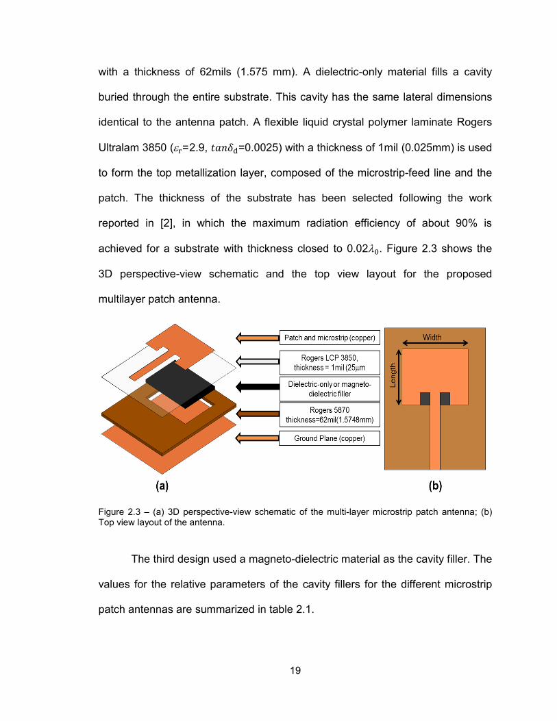
with a thickness of 62mils (1.575 mm). A dielectric-only material fills a cavity
buried through the entire substrate. This cavity has the same lateral dimensions
identical to the antenna patch. A flexible liquid crystal polymer laminate Rogers
Ultralam 3850 ( = 2.9, =0.0025) with a thickness of 1mil (0.025mm) is used
to form the top metallization layer, composed of the microstrip-feed line and the
patch. The thickness of the substrate has been selected following the work
reported in [2], in which the maximum radiation efficiency of about 90% is
achieved for a substrate with thickness closed to 0.02 . Figure 2.3 shows the
3D perspective-view schematic and the top view layout for the proposed
multilayer patch antenna.
Figure 2.3 – (a) 3D perspective-view schematic of the multi-layer microstrip patch antenna; (b) Top view layout of the antenna.
The third design used a magneto-dielectric material as the cavity filler. The
values for the relative parameters of the cavity fillers for the different microstrip
patch antennas are summarized in table 2.1.
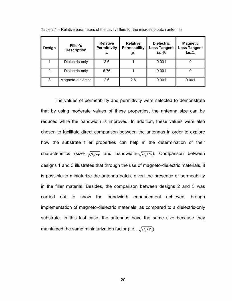
20
Table 2.1 – Relative parameters of the cavity fillers for the microstrip patch antennas
Design Filler’s Description
Relative Permittivity
r
Relative Permeability
r
Dielectric Loss Tangent
tand
Magnetic Loss Tangent
tanm
1 Dielectric-only 2.6 1 0.001 0
2 Dielectric-only 6.76 1 0.001 0
3 Magneto-dielectric 2.6 2.6 0.001 0.001
The values of permeability and permittivity were selected to demonstrate
that by using moderate values of these properties, the antenna size can be
reduced while the bandwidth is improved. In addition, these values were also
chosen to facilitate direct comparison between the antennas in order to explore
how the substrate filler properties can help in the determination of their
characteristics (size √ and bandwidth√
). Comparison between
designs 1 and 3 illustrates that through the use of magneto-dielectric materials, it
is possible to miniaturize the antenna patch, given the presence of permeability
in the filler material. Besides, the comparison between designs 2 and 3 was
carried out to show the bandwidth enhancement achieved through
implementation of magneto-dielectric materials, as compared to a dielectric-only
substrate. In this last case, the antennas have the same size because they
maintained the same miniaturization factor (i.e., √ .
21
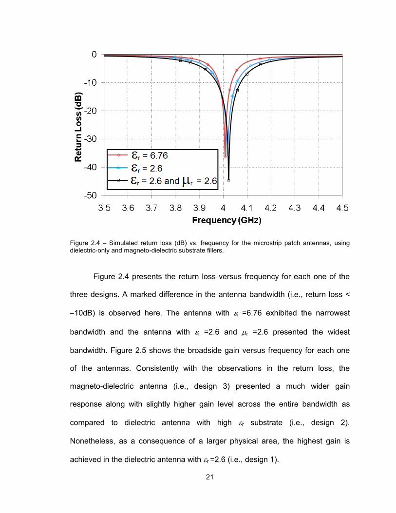
Figure 2.4 – Simulated return loss (dB) vs. frequency for the microstrip patch antennas, using dielectric-only and magneto-dielectric substrate fillers.
Figure 2.4 presents the return loss versus frequency for each one of the
three designs. A marked difference in the antenna bandwidth (i.e., return loss <
10dB) is observed here. The antenna with r =6.76 exhibited the narrowest
bandwidth and the antenna with r =2.6 and r =2.6 presented the widest
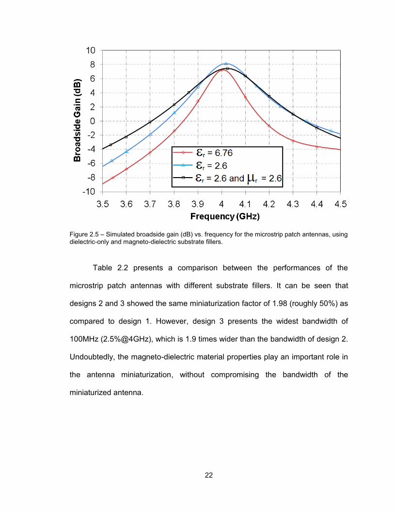
bandwidth. Figure 2.5 shows the broadside gain versus frequency for each one
of the antennas. Consistently with the observations in the return loss, the
magneto-dielectric antenna (i.e., design 3) presented a much wider gain
response along with slightly higher gain level across the entire bandwidth as
compared to dielectric antenna with high r substrate (i.e., design 2).
Nonetheless, as a consequence of a larger physical area, the highest gain is
achieved in the dielectric antenna with r =2.6 (i.e., design 1).
22
Figure 2.5 – Simulated broadside gain (dB) vs. frequency for the microstrip patch antennas, using dielectric-only and magneto-dielectric substrate fillers.
Table 2.2 presents a comparison between the performances of the
microstrip patch antennas with different substrate fillers. It can be seen that
designs 2 and 3 showed the same miniaturization factor of 1.98 (roughly 50%) as
compared to design 1. However, design 3 presents the widest bandwidth of
100MHz (2.5%@4GHz), which is 1.9 times wider than the bandwidth of design 2.
Undoubtedly, the magneto-dielectric material properties play an important role in
the antenna miniaturization, without compromising the bandwidth of the
miniaturized antenna.
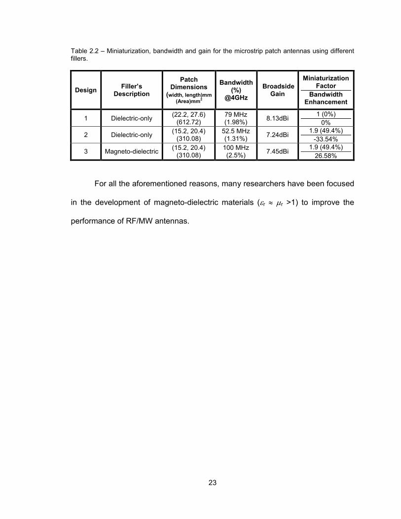
23
Table 2.2 – Miniaturization, bandwidth and gain for the microstrip patch antennas using different fillers.
Design Filler’s Description
Patch Dimensions
(width, length)mm (Area)mm2
Bandwidth (%)
@4GHz
Broadside Gain
Miniaturization Factor
Bandwidth Enhancement
1 Dielectric-only (22.2, 27.6) (612.72)
79 MHz (1.98%) 8.13dBi 1 (0%)
0%
2 Dielectric-only (15.2, 20.4) (310.08)
52.5 MHz (1.31%) 7.24dBi 1.9 (49.4%)
-33.54%
3 Magneto-dielectric (15.2, 20.4) (310.08)
100 MHz (2.5%) 7.45dBi 1.9 (49.4%)
26.58%
For all the aforementioned reasons, many researchers have been focused
in the development of magneto-dielectric materials (r r >1) to improve the
performance of RF/MW antennas.
24
Chapter 3
Fabrication and Characterization of Magnetite (Fe3O4) Polymer Nanocomposite
3.1 Introduction
This chapter presents some background on the fabrication and
characterization of the materials used for engineering the magneto-dielectric
substrate. Fabrication of polymer nanocomposites using polymeric matrices is
herein explained in detail. In the last section, the physical dielectric and magnetic
properties of the materials were extracted to analyze their impact on RF and
microwave applications.
The nanoparticles implemented in this dissertation work are made of
magnetite (Fe3O4). This material is a common magnetic iron oxide that has a
cubic inverse spinel structure with oxygen forming a face centered cubic (FCC)
closed packing, in which iron (Fe) cations occupy interstitial tetrahedral sites and
octahedral sites [8][9]. The electrons can hop between Fe2+ and Fe3+ ions in the
octahedral sites at room temperature, rendering magnetite as an important class
of half-metallic material [8]. In the past, magnetite nanoparticles have been used
as ferrofluids (e.g. rotary shaft sealing, oscillation damping, and position sensing)
[8].
Biomedical and biological applications have also been targeted by using
surface treated nanoparticles. Using the proper chemical treatment and
surfactants, magnetic nanoparticles had been dispersed into water and other
25
biocompatible solvents [8][10]. Such a suspension is very useful in application
where external magnetic fields are applied for positioning in specific areas,
facilitating image diagnosis (i.e., magnetic resonance imaging) and assisted
cancer therapy (i.e., killing cancer cells selectively by the heat generated due to
hysteresis) [8][11].
Substrates and materials used for RF and microwave antenna
implementation are required to have low dielectric and magnetic losses. For this
reason, magneto-dielectric polymer nanocomposites must retain the
superparamagnetic properties presented in the nanoparticles, avoiding clustering
formation and achieving an excellent dispersion and interaction with the
polymeric matrix. Additionally, nanoparticles with a narrow size distribution are
required to obtain homogeneous interaction between them, for which the
particles must be uniform in their physical and chemical properties [8].
Nonetheless, it is very difficult to produce non-agglomerated magnetite
nanoparticles with a desired size and a narrow size distribution. By means of the
synthesis process that is described in the following section, it is possible to obtain
polymer nanocomposites with excellent monodispersion of magnetite
nanoparticles.
3.2 Setup for Synthesis of Magnetite (Fe3O4) Nanoparticles
The nanoparticle synthesis follows a chemical procedure that requires a
special setup that guarantees a controlled and stable environment, necessary to
obtain particles with the right chemical composition and a tight size distribution.
The reaction takes place in a 500ml three neck flask where all the chemicals are
26
combined. This vessel was laid on a heating mantle/magnetic stirrer setup. The
center neck of the flask is connected to an allihn condenser, while the necks to
the right and the left are connected to a thermocouple and a needle with
controlled argon flow, respectively. The allihn condenser helps in the reflux of the
solution that is heated above its boiling point. The thermocouple provides the
feedback to a temperature controller which provides the power to the heating
mantle.
3.3 Synthesis of Magnetite (Fe3O4) Nanoparticles
In this dissertation work, Fe3O4 nanoparticles are synthesized via thermal
decomposition reaction. Several chemicals are used for the synthesis of
magnetite nanoparticles, including Iron(III) acetylacetonate (99.9 trace metal
basis, also known as Fe(acac)3), oleylamine (technical grade,70%), ethanol (200
proof, anhydrous, 99.5%), hexane (anhydrous, 95%), benzyl ether (98%) and
oleic acid. All these chemicals were not modified to any extent and used as
received.
Following a standard chemical procedure, Magnetite (Fe3O4)
nanoparticles with an average size of 7 nm and coated with surfactants
(oleylamine and oleic acid) are synthesized similar to what has been reported in
[8][10]-[18]. Ten (10) mmol iron(III) acetylacetonate, 50 mL of oleylamine and 50
mL of benzyl ether are combined in a 500ml three-neck bottom rounded flask.
The mixture is magnetically stirred under a continuous flow of argon at room
temperature for 5 minutes. For dehydration purposes, the mixture is heated at
110C for 1h, using a heating rate of 20C/min. Subsequently, the sample is
27
quickly heated to reflux at 300C for 2h, using the same 20C/min heating rate.
During the complete process, the sample is magnetically stirred to ensure
homogeneity during the mixing process. Also, a continuous flow of argon gas is
kept to maintain an inert environment. The resultant black colored solution is
cooled to room temperature followed by addition of 200ml of ethanol into the
solution. The precipitate is collected by centrifugation at 5000 rpm for 5 minutes
of duration and washed with ethanol several times.
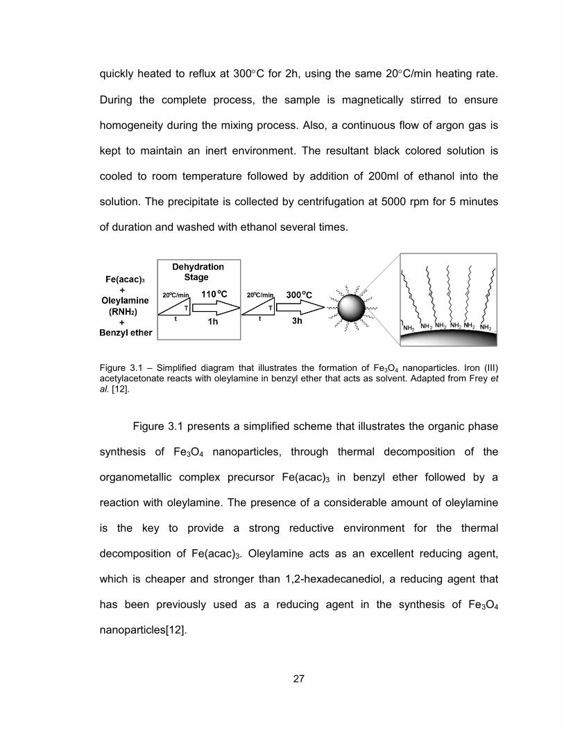
Figure 3.1 – Simplified diagram that illustrates the formation of Fe3O4 nanoparticles. Iron (III) acetylacetonate reacts with oleylamine in benzyl ether that acts as solvent. Adapted from Frey et al. [12].
Figure 3.1 presents a simplified scheme that illustrates the organic phase
synthesis of Fe3O4 nanoparticles, through thermal decomposition of the
organometallic complex precursor Fe(acac)3 in benzyl ether followed by a
reaction with oleylamine. The presence of a considerable amount of oleylamine
is the key to provide a strong reductive environment for the thermal
decomposition of Fe(acac)3. Oleylamine acts as an excellent reducing agent,
which is cheaper and stronger than 1,2-hexadecanediol, a reducing agent that
has been previously used as a reducing agent in the synthesis of Fe3O4
nanoparticles[12].
28
Fe(acac)3 is a metal carbonyl with strong tendency to dissociate the
carbonyl groups when heated, leaving the zero-valent metal centers to nucleate
and grow into nanoparticles[11]. However, the resultant nanoparticles are
extremely reactive and subject to fast oxidation. Oleylamine acts as an efficient
surface coating that prevents oxygen to penetrate and react with the
nanoparticle. The coating is created by the interaction of the NH2 group, existing
in the oleylamine chemical structure, with the surface of the nanoparticles. The
surface coating process with a non-polar surfactant such as oleylamine, results in
nanoparticles with hydrophobic characteristics.
Given the non-polarity of oleylamine, and its implementation as
nanoparticle surface coating, a stable nanoparticles suspension requires a
nonpolar or weakly polar hydrocarbon solvent, such as toluene or hexane. The
synthesized Fe3O4 nanoparticles were then suspended in a mixture of hexane
(anhydrous, 95%) with 0.05 ml of oleylamine and 0.05ml of oleic acid. The
presence of these two surfactants helps stabilize the particles in hexane for a
longer period of time. Finally, the product is dried at room temperature when
needed. By using this synthesis technique and the amounts of chemicals
specified above, a successful experiment produces 0.650.2g of Fe3O4
nanoparticles.
3.4 Characterization of Magnetite (Fe3O4) Nanoparticles
3.4.1 Characterization of Nanoparticles Using X-Ray Diffraction
X-Ray Diffraction (XRD) measurements are made to analyze the
crystallographic structure of magnetite (Fe3O4) nanoparticles. The sample is
29
prepared on a 2 inch silicon wafer with a well-recognized response when XRD is
performed. As the particles are suspended in hexane and a layer coating with
significant thickness is required for the XRD analysis, silicone adhesive resin is
used to cast a rectangular shape receptacle that facilitates the deposition of the
magnetite nanoparticle solution. Using a Pasteur pipette, several drops are
deposited inside the receptacle and the hexane is evaporated at room
temperature. After several repetitions, a layer with the desired thickness for the
XRD measurements is obtained.
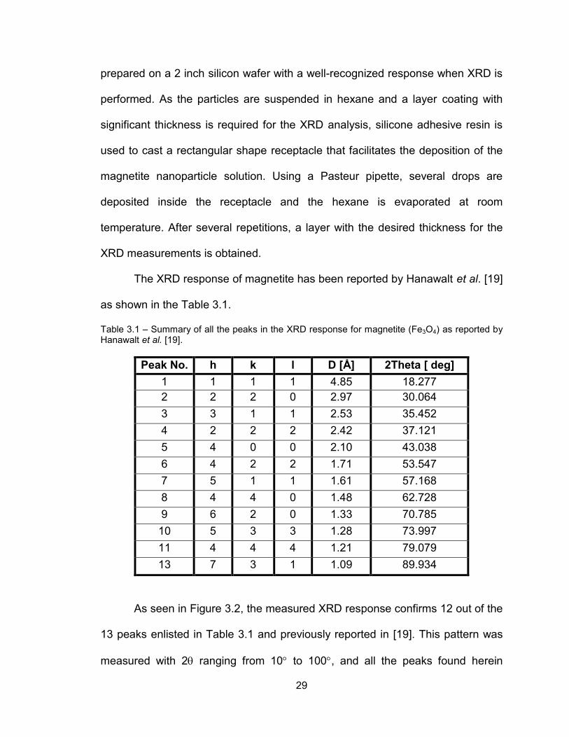
The XRD response of magnetite has been reported by Hanawalt et al. [19]
as shown in the Table 3.1.
Table 3.1 – Summary of all the peaks in the XRD response for magnetite (Fe3O4) as reported by Hanawalt et al. [19].
Peak No. h k l D [Å] 2Theta [ deg] 1 1 1 1 4.85 18.277 2 2 2 0 2.97 30.064 3 3 1 1 2.53 35.452 4 2 2 2 2.42 37.121 5 4 0 0 2.10 43.038 6 4 2 2 1.71 53.547 7 5 1 1 1.61 57.168 8 4 4 0 1.48 62.728 9 6 2 0 1.33 70.785 10 5 3 3 1.28 73.997 11 4 4 4 1.21 79.079 13 7 3 1 1.09 89.934
As seen in Figure 3.2, the measured XRD response confirms 12 out of the
13 peaks enlisted in Table 3.1 and previously reported in [19]. This pattern was
measured with 2 ranging from 10 to 100, and all the peaks found herein
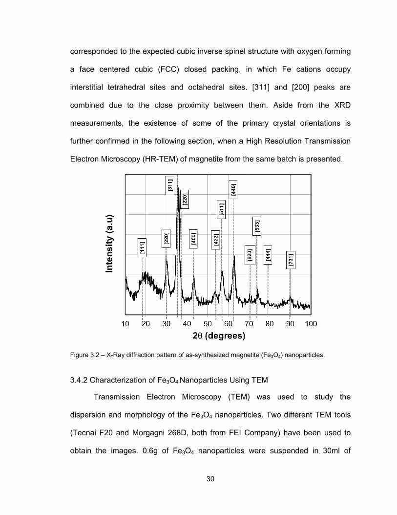
30
corresponded to the expected cubic inverse spinel structure with oxygen forming
a face centered cubic (FCC) closed packing, in which Fe cations occupy
interstitial tetrahedral sites and octahedral sites. [311] and [200] peaks are
combined due to the close proximity between them. Aside from the XRD
measurements, the existence of some of the primary crystal orientations is
further confirmed in the following section, when a High Resolution Transmission
Electron Microscopy (HR-TEM) of magnetite from the same batch is presented.
Figure 3.2 – X-Ray diffraction pattern of as-synthesized magnetite (Fe3O4) nanoparticles.
3.4.2 Characterization of Fe3O4 Nanoparticles Using TEM
Transmission Electron Microscopy (TEM) was used to study the
dispersion and morphology of the Fe3O4 nanoparticles. Two different TEM tools
(Tecnai F20 and Morgagni 268D, both from FEI Company) have been used to
obtain the images. 0.6g of Fe3O4 nanoparticles were suspended in 30ml of
31
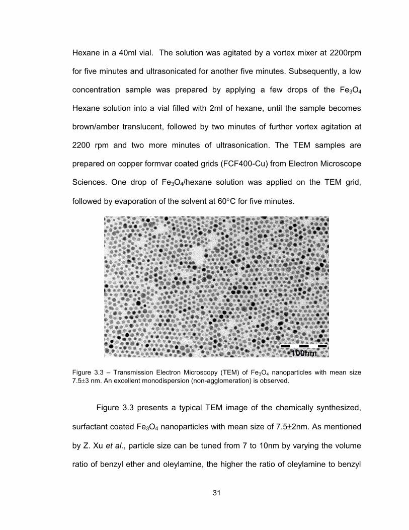
Hexane in a 40ml vial. The solution was agitated by a vortex mixer at 2200rpm
for five minutes and ultrasonicated for another five minutes. Subsequently, a low
concentration sample was prepared by applying a few drops of the Fe3O4
Hexane solution into a vial filled with 2ml of hexane, until the sample becomes
brown/amber translucent, followed by two minutes of further vortex agitation at
2200 rpm and two more minutes of ultrasonication. The TEM samples are
prepared on copper formvar coated grids (FCF400-Cu) from Electron Microscope
Sciences. One drop of Fe3O4/hexane solution was applied on the TEM grid,
followed by evaporation of the solvent at 60C for five minutes.
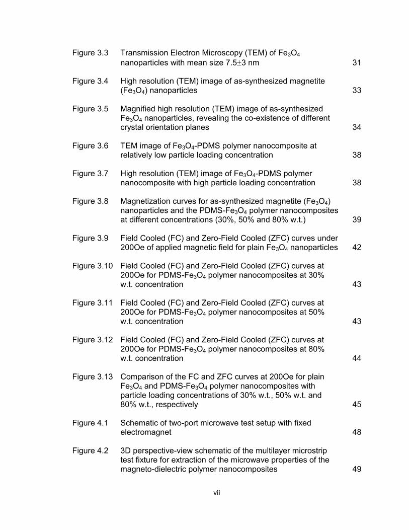
Figure 3.3 – Transmission Electron Microscopy (TEM) of Fe3O4 nanoparticles with mean size 7.53 nm. An excellent monodispersion (non-agglomeration) is observed.
Figure 3.3 presents a typical TEM image of the chemically synthesized,
surfactant coated Fe3O4 nanoparticles with mean size of 7.52nm. As mentioned
by Z. Xu et al., particle size can be tuned from 7 to 10nm by varying the volume
ratio of benzyl ether and oleylamine, the higher the ratio of oleylamine to benzyl
32
ether, the smaller the resultant Fe3O4 nanoparticles [12]. In their experiment, 7nm
Fe3O4 nanoparticles were obtained using oleylamine only and 10nm
nanoparticles were obtained using a 1:1 volume ratio of oleylamine to benzyl
ether. As shown in Figure 3.3 and Figure 3.4, for the process developed for this
dissertation work, the size of the synthesized nanoparticles is 7.5nm2nm, which
implies that even smaller nanoparticles (below the minimum size reported in [12])
can be obtained by increasing the ratio of oleylamine to benzyl ether.
As seen in Figure 3.3 and Figure 3.4, Fe3O4 nanoparticles do not form
clusters, as a consequence of the surface modification performed during the
synthesis and suspension process. Nanoparticles are surface functionalized,
coated by oleylamine and oleic acid, which prevents their agglomeration.
Oleylamine and oleic acid also act as a buffer between the magnetic particles to
ensure there is minimum level of interaction or coupling between them, even if
they have physical contact. This would allow the nanoparticles to display largely
non-interacting or a weakly interacting superparamagnetic response [18].
33
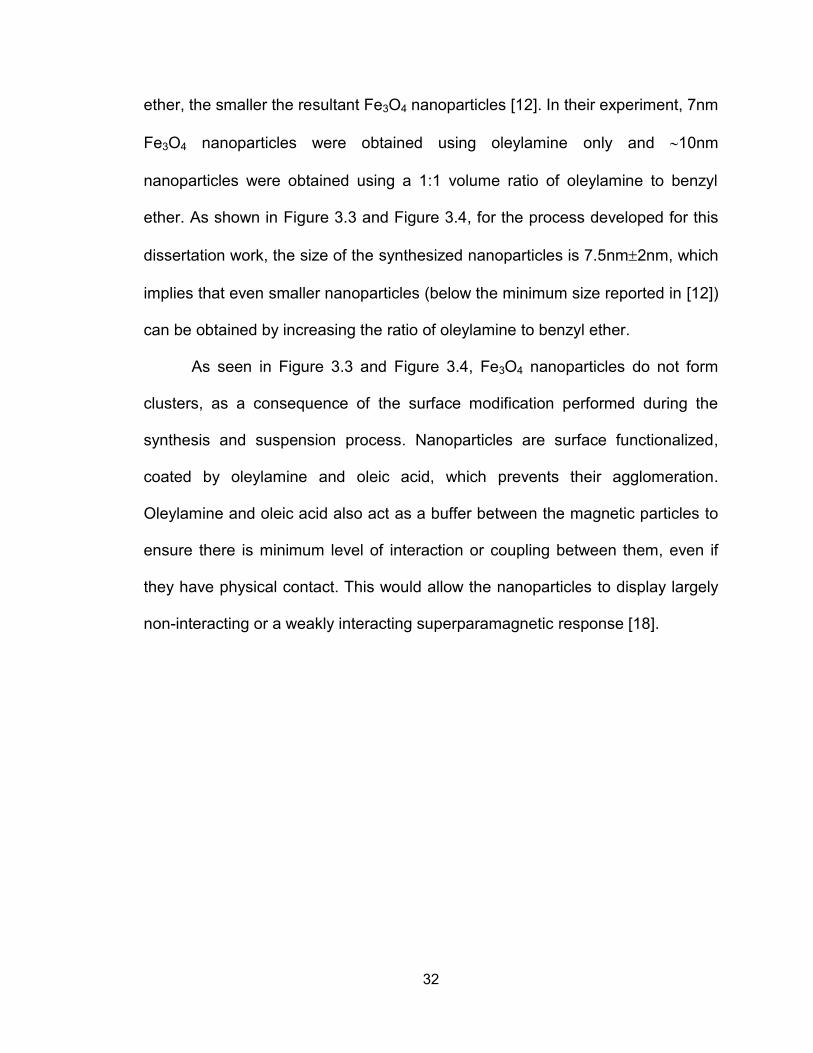
Figure 3.4 – High resolution (TEM) image of as-synthesized magnetite (Fe3O4) nanoparticles.
Figure 3.3 presents a high resolution TEM image of the Fe3O4
nanoparticles prepared on top of a TEM grid, indicating all the particles have a
well-defined rounded shape. In addition, this TEM image also confirms the
measured nanoparticle size distribution of 7.52nm. Aside from their shapes, a
blurry region surrounding each nanoparticle can be observed in the magnified
TEM image shown in Figure 3.5. The irregular shape of this blurry region could
be ascribed to the presence of the surfactant coating on the particles instead of
an effect caused by the particle interaction with the electron beam or possible
lens aberration.
34
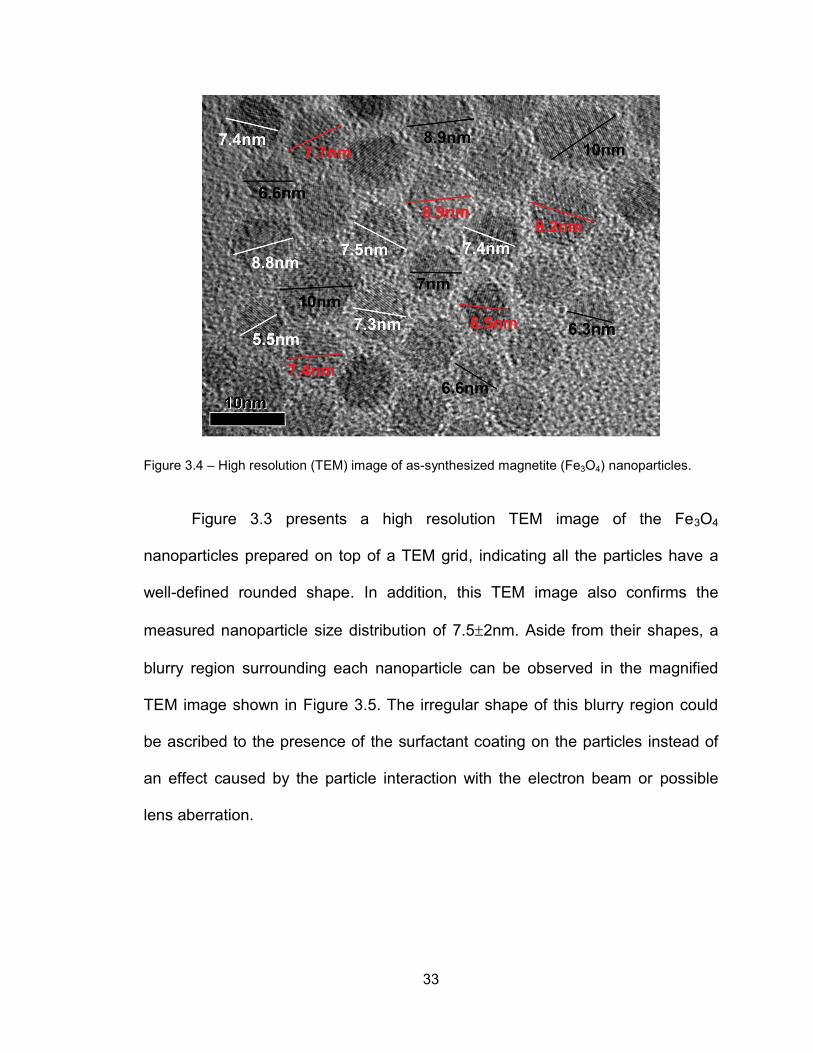
Figure 3.5 – Magnified high resolution (TEM) image of as-synthesized Fe3O4 nanoparticles, revealing the co-existence of different crystal orientation planes.
Figure 3.5 also shows the presence of the crystal orientation planes for
the as-synthesized Fe3O4 nanoparticles. Interplanar distances were measured
and compared with those reported by Hanawalt et al. [19]. The crystallographic
orientation found in this image denotes the existence of [2 0 0], [4 0 0] and [2 2 2]
planes, with interatomic spacing (d-spacing) of 2.9Å, 2.45Å and 2.1Å,
respectively. As shown in Figure 3.5, each particle holds a different orientation of
their crystal planes, which depicts that particle-to-particle interaction does not
cause alignment of the particles in a specific direction. The suspended
nanoparticles do not have a common crystal orientation as exhibited by bulk
magnetic materials. This can explain why the effective magnetic properties of
35
nanocomposites are very difficult to specify and the presence of permeability and
permittivity tensors is not easy to demonstrate or model.
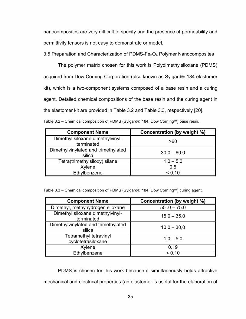
3.5 Preparation and Characterization of PDMS-Fe3O4 Polymer Nanocomposites
The polymer matrix chosen for this work is Polydimethylsiloxane (PDMS)
acquired from Dow Corning Corporation (also known as Sylgard 184 elastomer
kit), which is a two-component systems composed of a base resin and a curing
agent. Detailed chemical compositions of the base resin and the curing agent in
the elastomer kit are provided in Table 3.2 and Table 3.3, respectively [20].
Table 3.2 – Chemical composition of PDMS (Sylgard 184, Dow Corning) base resin.
Component Name Concentration (by weight %) Dimethyl siloxane dimethylvinyl-
terminated >60
Dimethylvinylated and trimethylated silica 30.0 – 60.0
Tetra(trimethylsiloxy) silane 1.0 – 5.0 Xylene 0.5
Ethylbenzene < 0.10
Table 3.3 – Chemical composition of PDMS (Sylgard 184, Dow Corning) curing agent.
Component Name Concentration (by weight %) Dimethyl, methyhydrogen siloxane 55 .0 – 75.0
Dimethyl siloxane dimethylvinyl-terminated 15.0 – 35.0
Dimethylvinylated and trimethylated silica 10.0 – 30,0
Tetramethyl tetravinyl cyclotetrasiloxane 1.0 – 5.0
Xylene 0.19 Ethylbenzene < 0.10
PDMS is chosen for this work because it simultaneously holds attractive
mechanical and electrical properties (an elastomer is useful for the elaboration of
36
flexible electronics) while allowing ease of processing. In particular, Sylgard
184 can be cured at low temperature (@90C for 45min), safeguarding the
integrity of nanoparticles during the curing process.
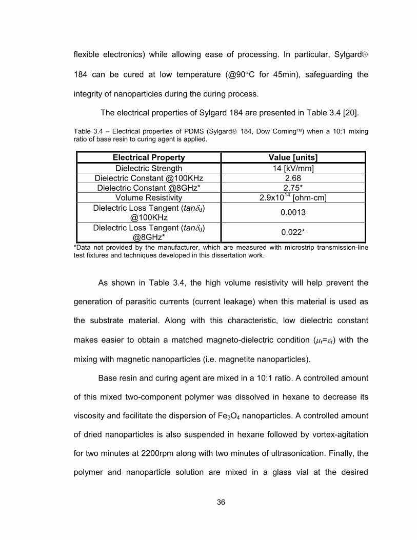
The electrical properties of Sylgard 184 are presented in Table 3.4 [20].
Table 3.4 – Electrical properties of PDMS (Sylgard 184, Dow Corning) when a 10:1 mixing ratio of base resin to curing agent is applied.
Electrical Property Value [units] Dielectric Strength 14 [kV/mm]
Dielectric Constant @100KHz 2.68 Dielectric Constant @8GHz* 2.75*
Volume Resistivity 2.9x10¹⁴ [ohm-cm] Dielectric Loss Tangent (tand)
@100KHz 0.0013
Dielectric Loss Tangent (tand) @8GHz* 0.022*
*Data not provided by the manufacturer, which are measured with microstrip transmission-line test fixtures and techniques developed in this dissertation work.
As shown in Table 3.4, the high volume resistivity will help prevent the
generation of parasitic currents (current leakage) when this material is used as
the substrate material. Along with this characteristic, low dielectric constant
makes easier to obtain a matched magneto-dielectric condition (r=r) with the
mixing with magnetic nanoparticles (i.e. magnetite nanoparticles).
Base resin and curing agent are mixed in a 10:1 ratio. A controlled amount
of this mixed two-component polymer was dissolved in hexane to decrease its
viscosity and facilitate the dispersion of Fe3O4 nanoparticles. A controlled amount
of dried nanoparticles is also suspended in hexane followed by vortex-agitation
for two minutes at 2200rpm along with two minutes of ultrasonication. Finally, the
polymer and nanoparticle solution are mixed in a glass vial at the desired
37
concentration, followed by vortex agitation for five minutes and ultrasonication for
4 minutes.
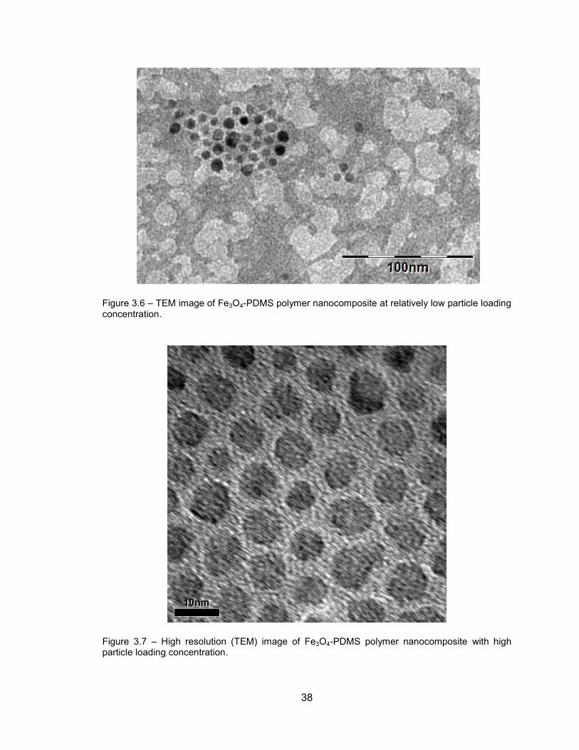
3.5.1 Characterization of PDMS-Fe3O4 Nanocomposites Using TEM
The TEM samples are prepared on copper formvar coated grids (FCF400-
Cu) from Electron Microscope Sciences. One drop of the Fe3O4-PDMS
nanocomposite solution was applied on the TEM grid, followed by evaporation of
the solvent and curing at 90C during four hours under 30 inHg of vacuum.
Figure 3.6 presents the TEM image of the polymer nanocomposite, showing an
excellent polymer-to-particle interaction. Nanoparticles tend to form islands,
showing the existence of weak interactions between them. However, each
nanoparticle can be individually observed and differentiated among the others,
revealing the non-agglomeration of the particles while embedded in the polymeric
matrix.
In order to confirm the good interaction between polymer matrix and
nanoparticles, a new sample is prepared with slightly elevated concentration of
particles. Figure 3.7 presents a HR-TEM image of the high loading concentration
polymer nanocomposites, confirming the highly uniform dispersion of the
particles in the polymer matrix. Given that the nanoparticles are covered by a
layer of PDMS, it is very difficult to reach optimal focus on the particles, and thus
the atomic crystal orientation of the particles is not easily observed.
38
Figure 3.6 – TEM image of Fe3O4-PDMS polymer nanocomposite at relatively low particle loading concentration.
Figure 3.7 – High resolution (TEM) image of Fe3O4-PDMS polymer nanocomposite with high particle loading concentration.
39
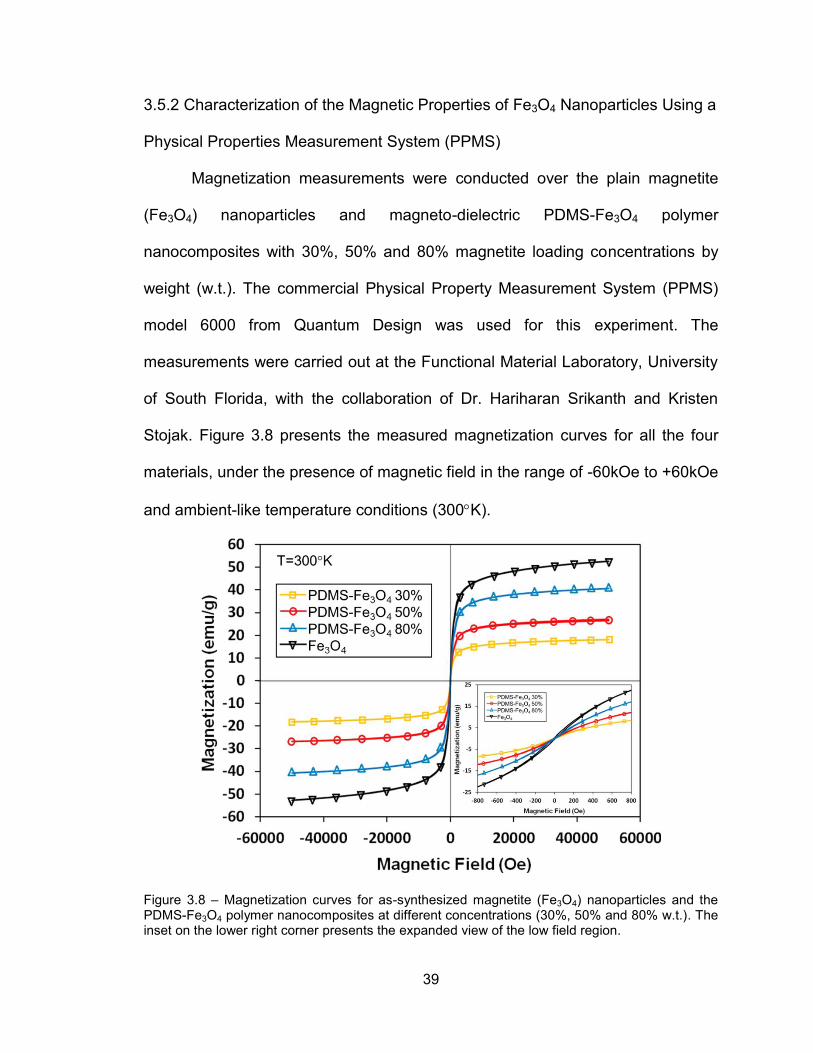
3.5.2 Characterization of the Magnetic Properties of Fe3O4 Nanoparticles Using a
Physical Properties Measurement System (PPMS)
Magnetization measurements were conducted over the plain magnetite
(Fe3O4) nanoparticles and magneto-dielectric PDMS-Fe3O4 polymer
nanocomposites with 30%, 50% and 80% magnetite loading concentrations by
weight (w.t.). The commercial Physical Property Measurement System (PPMS)
model 6000 from Quantum Design was used for this experiment. The
measurements were carried out at the Functional Material Laboratory, University
of South Florida, with the collaboration of Dr. Hariharan Srikanth and Kristen
Stojak. Figure 3.8 presents the measured magnetization curves for all the four
materials, under the presence of magnetic field in the range of -60kOe to +60kOe
and ambient-like temperature conditions (300K).
Figure 3.8 – Magnetization curves for as-synthesized magnetite (Fe3O4) nanoparticles and the PDMS-Fe3O4 polymer nanocomposites at different concentrations (30%, 50% and 80% w.t.). The inset on the lower right corner presents the expanded view of the low field region.
40
The inset in the lower right corner depicts the absence of magnetic
hysteresis at ambient temperature (300K) under all three particle loading
concentrations, confirming the retention of superparamagnetism for all the
materials under test. This is a highly desirable condition that is crucial for low loss
RF/microwave materials. Such a property can only be realized through a
combination of effective nanoparticle surface functionalization, homogenous
nanoparticle dispersion and excellent interaction between the nanoparticles and
the PDMS matrix. Furthermore, saturation magnetization ( ) values were
extracted from magnetization curves, leading to a of 81emu/g for plain Fe3O4
nanoparticles. Besides, the PDMS-Fe3O4 nanocomposites at 80%, 50% and 30%
loading concentrations have exhibited values of 40.44emu/g, 27.06emu/g and
18.12emu/g, respectively. The increase of the with incremented particle
loading concentration, was expected to occur given the increasing of the
magnetic material volume concentration in the PNCs [14][16].
To complete the magnetic characterization, magnetization vs. temperature
measurements were also carried out in the temperature range from 10K to
300K and vice versa. Both field cooled (FC) and zero field cooled (ZFC)
measurements were carried out as they provided relevant material
characteristics; specifically, the blocking temperature ( ) for the nanoparticles
and polymer nanocomposite systems corresponds to the temperature where the
maximum of the ZFC curve occurs. The blocking temperature of the
nanoparticles marks the temperature above which the particles are
superparamagnetic. It is therefore critical to keep the blocking temperature below
41
the ambient temperature, under which most of the electronics and RF and
microwave devices operate. Furthermore, other information details concerning to
the nanoparticle size distribution, particle to particle interaction and nanoparticle
clustering could be inferred from the FC and ZFC measurement results.
of a single domain particle can be described as follows [16]:
(3.1)
where is the magnetocrystalline anisotropy, is the volume of the nanoparticle
and is the Boltzmann constant. As is related to the volume of the
nanoparticles, the peak width at the ZFC curve is related to the relaxation time
distribution and correspondingly to the particle size distribution in the sample
[16].
Many studies have revealed the increase of when the average inter-
particle distance is decreased, which could be ascribed to dipolar interactions
between the particles [16]. This also opens the possibility of widening of the ZFC
peak due to the presence of a small amount of nanoparticles clustering. In this
case, the agglomerated particles must be small enough to maintain single-
domain systems, thus allowing the retention of superparamagnetic properties for
the bulk material.
Figure 3.9 depicts the FC and ZFC curves at 200Oe of externally applied
magnetic field obtained from plain Fe3O4 nanoparticles. The results presented in
this figure are characteristic of a single domain nanoparticle system with a
blocking temperature =81K. The data shown in Figure 3.9 along with the
hysteresis loop measurements, demonstrate that the Fe3O4 nanoparticle system
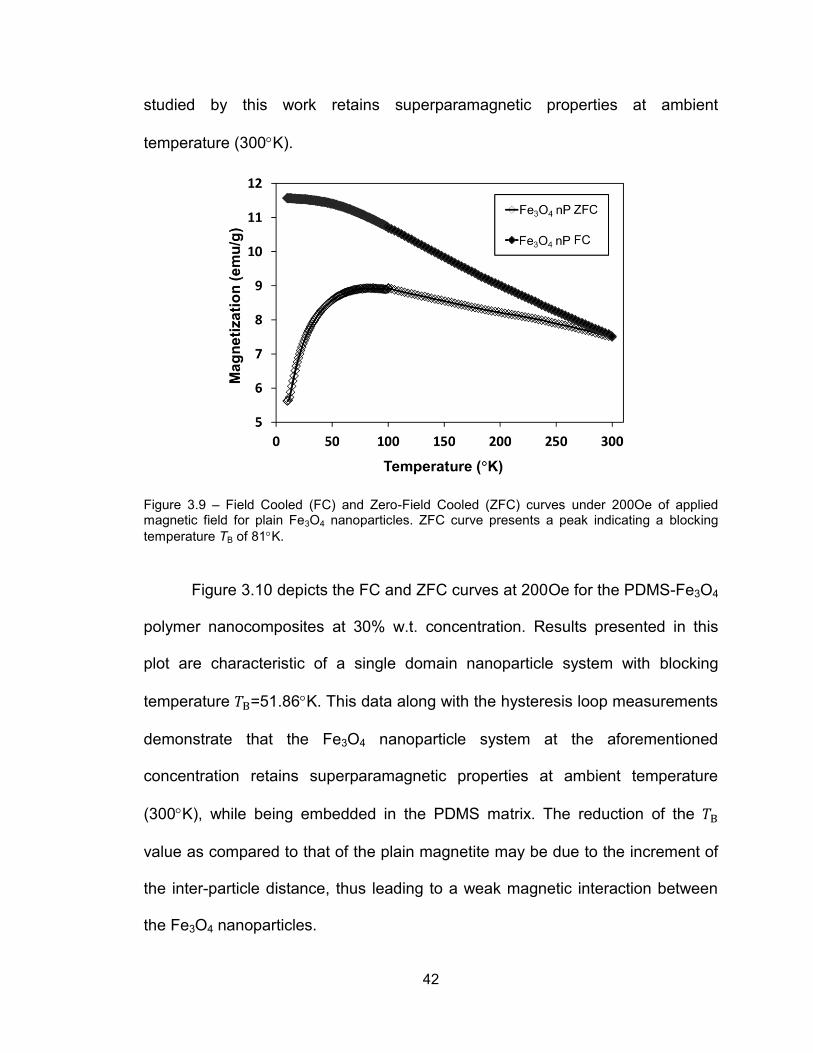
42
studied by this work retains superparamagnetic properties at ambient
temperature (300K).
Figure 3.9 – Field Cooled (FC) and Zero-Field Cooled (ZFC) curves under 200Oe of applied magnetic field for plain Fe3O4 nanoparticles. ZFC curve presents a peak indicating a blocking temperature TB of 81K.
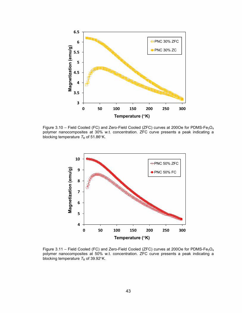
Figure 3.10 depicts the FC and ZFC curves at 200Oe for the PDMS-Fe3O4
polymer nanocomposites at 30% w.t. concentration. Results presented in this
plot are characteristic of a single domain nanoparticle system with blocking
temperature =51.86K. This data along with the hysteresis loop measurements
demonstrate that the Fe3O4 nanoparticle system at the aforementioned
concentration retains superparamagnetic properties at ambient temperature
(300K), while being embedded in the PDMS matrix. The reduction of the
value as compared to that of the plain magnetite may be due to the increment of
the inter-particle distance, thus leading to a weak magnetic interaction between
the Fe3O4 nanoparticles.
43
Figure 3.10 – Field Cooled (FC) and Zero-Field Cooled (ZFC) curves at 200Oe for PDMS-Fe3O4 polymer nanocomposites at 30% w.t. concentration. ZFC curve presents a peak indicating a blocking temperature TB of 51.86K.
Figure 3.11 – Field Cooled (FC) and Zero-Field Cooled (ZFC) curves at 200Oe for PDMS-Fe3O4 polymer nanocomposites at 50% w.t. concentration. ZFC curve presents a peak indicating a blocking temperature TB of 39.92K.
44
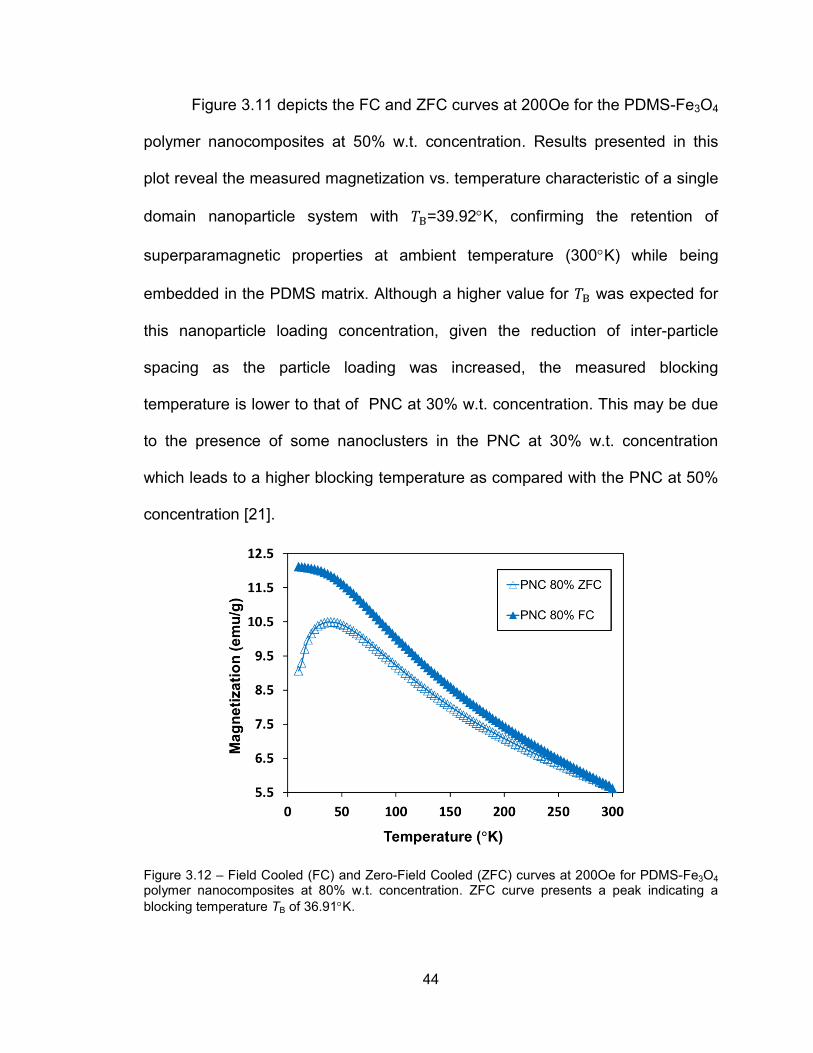
Figure 3.11 depicts the FC and ZFC curves at 200Oe for the PDMS-Fe3O4
polymer nanocomposites at 50% w.t. concentration. Results presented in this
plot reveal the measured magnetization vs. temperature characteristic of a single
domain nanoparticle system with =39.92K, confirming the retention of
superparamagnetic properties at ambient temperature (300K) while being
embedded in the PDMS matrix. Although a higher value for was expected for
this nanoparticle loading concentration, given the reduction of inter-particle
spacing as the particle loading was increased, the measured blocking
temperature is lower to that of PNC at 30% w.t. concentration. This may be due
to the presence of some nanoclusters in the PNC at 30% w.t. concentration
which leads to a higher blocking temperature as compared with the PNC at 50%
concentration [21].
Figure 3.12 – Field Cooled (FC) and Zero-Field Cooled (ZFC) curves at 200Oe for PDMS-Fe3O4 polymer nanocomposites at 80% w.t. concentration. ZFC curve presents a peak indicating a blocking temperature TB of 36.91K.
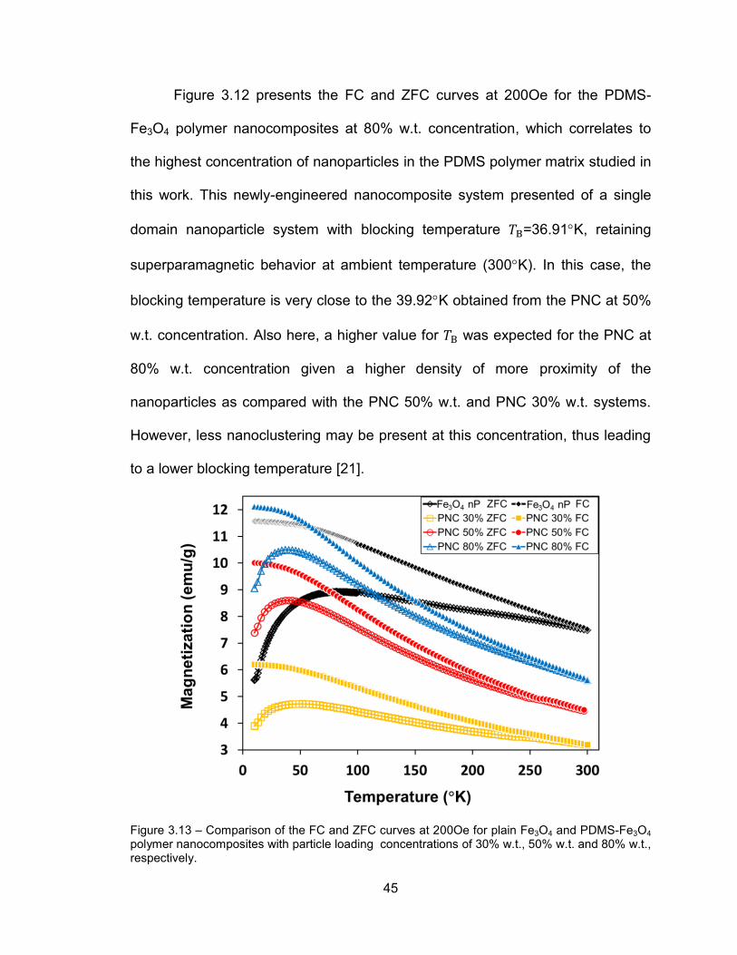
45
Figure 3.12 presents the FC and ZFC curves at 200Oe for the PDMS-
Fe3O4 polymer nanocomposites at 80% w.t. concentration, which correlates to
the highest concentration of nanoparticles in the PDMS polymer matrix studied in
this work. This newly-engineered nanocomposite system presented of a single
domain nanoparticle system with blocking temperature =36.91K, retaining
superparamagnetic behavior at ambient temperature (300K). In this case, the
blocking temperature is very close to the 39.92K obtained from the PNC at 50%
w.t. concentration. Also here, a higher value for was expected for the PNC at
80% w.t. concentration given a higher density of more proximity of the
nanoparticles as compared with the PNC 50% w.t. and PNC 30% w.t. systems.
However, less nanoclustering may be present at this concentration, thus leading
to a lower blocking temperature [21].
Figure 3.13 – Comparison of the FC and ZFC curves at 200Oe for plain Fe3O4 and PDMS-Fe3O4 polymer nanocomposites with particle loading concentrations of 30% w.t., 50% w.t. and 80% w.t., respectively.
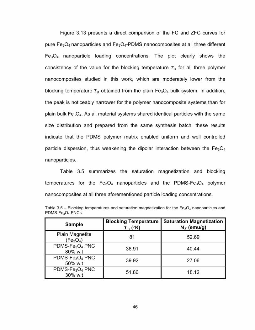
46
Figure 3.13 presents a direct comparison of the FC and ZFC curves for
pure Fe3O4 nanoparticles and Fe3O4-PDMS nanocomposites at all three different
Fe3O4 nanoparticle loading concentrations. The plot clearly shows the
consistency of the value for the blocking temperature for all three polymer
nanocomposites studied in this work, which are moderately lower from the
blocking temperature obtained from the plain Fe3O4 bulk system. In addition,
the peak is noticeably narrower for the polymer nanocomposite systems than for
plain bulk Fe3O4. As all material systems shared identical particles with the same
size distribution and prepared from the same synthesis batch, these results
indicate that the PDMS polymer matrix enabled uniform and well controlled
particle dispersion, thus weakening the dipolar interaction between the Fe3O4
nanoparticles.
Table 3.5 summarizes the saturation magnetization and blocking
temperatures for the Fe3O4 nanoparticles and the PDMS-Fe3O4 polymer
nanocomposites at all three aforementioned particle loading concentrations.
Table 3.5 – Blocking temperatures and saturation magnetization for the Fe3O4 nanoparticles and PDMS-Fe3O4 PNCs.
Sample Blocking Temperature (K)
Saturation Magnetization (emu/g)
Plain Magnetite (Fe3O4)
81 52.69
PDMS-Fe3O4 PNC 80% w.t 36.91 40.44
PDMS-Fe3O4 PNC 50% w.t 39.92 27.06
PDMS-Fe3O4 PNC 30% w.t 51.86 18.12
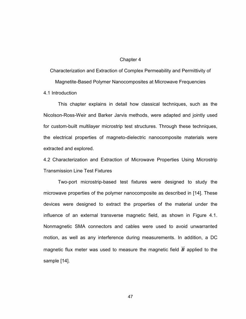
47
Chapter 4
Characterization and Extraction of Complex Permeability and Permittivity of
Magnetite-Based Polymer Nanocomposites at Microwave Frequencies
4.1 Introduction
This chapter explains in detail how classical techniques, such as the
Nicolson-Ross-Weir and Barker Jarvis methods, were adapted and jointly used
for custom-built multilayer microstrip test structures. Through these techniques,
the electrical properties of magneto-dielectric nanocomposite materials were
extracted and explored.
4.2 Characterization and Extraction of Microwave Properties Using Microstrip
Transmission Line Test Fixtures
Two-port microstrip-based test fixtures were designed to study the
microwave properties of the polymer nanocomposite as described in [14]. These
devices were designed to extract the properties of the material under the
influence of an external transverse magnetic field, as shown in Figure 4.1.
Nonmagnetic SMA connectors and cables were used to avoid unwarranted
motion, as well as any interference during measurements. In addition, a DC
magnetic flux meter was used to measure the magnetic field ⃑⃑ applied to the
sample [14].
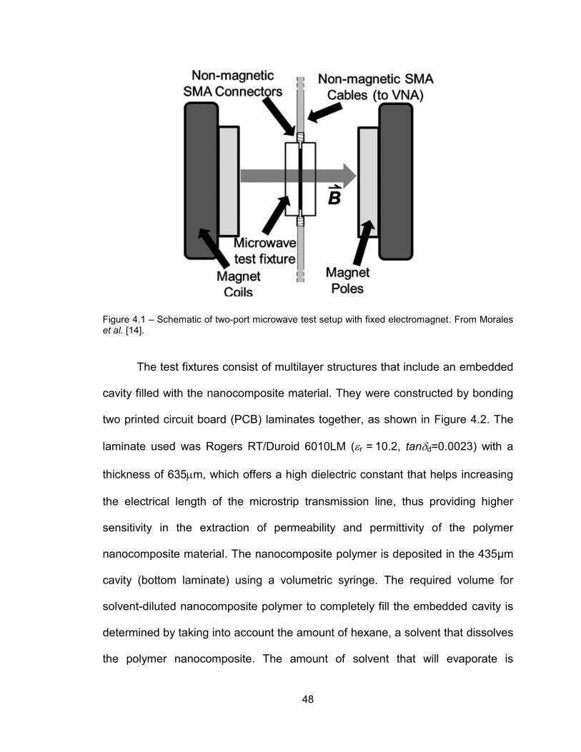
48
Figure 4.1 – Schematic of two-port microwave test setup with fixed electromagnet. From Morales et al. [14].
The test fixtures consist of multilayer structures that include an embedded
cavity filled with the nanocomposite material. They were constructed by bonding
two printed circuit board (PCB) laminates together, as shown in Figure 4.2. The
laminate used was Rogers RT/Duroid 6010LM (r = 10.2, tand=0.0023) with a
thickness of 635m, which offers a high dielectric constant that helps increasing
the electrical length of the microstrip transmission line, thus providing higher
sensitivity in the extraction of permeability and permittivity of the polymer
nanocomposite material. The nanocomposite polymer is deposited in the 435µm
cavity (bottom laminate) using a volumetric syringe. The required volume for
solvent-diluted nanocomposite polymer to completely fill the embedded cavity is
determined by taking into account the amount of hexane, a solvent that dissolves
the polymer nanocomposite. The amount of solvent that will evaporate is
49
considered in the total volume calculation of the applied material. After curing,
profilometer measurements demonstrated a difference of less than 0.5µm
between the heights of the substrate and the deposited material [14].
Figure 4.2 – 3D perspective-view schematic of the multilayer microstrip test fixture for extraction of the microwave properties of the magneto-dielectric polymer nanocomposites. From Morales et al. [14].
Thereafter, the bottom laminate containing the sample was heated in a
vacuum oven at 90C and 27inHg of vacuum for 4 hours to cure the composite
materials. The vacuum is applied in order to prevent oxidation or annealing of the
sample. Thus, it would be beneficial to purge the oven using Nitrogen or Argon
gas before vacuum is applied. Finally, the top laminate is attached to the bottom
one using a very thin layer of epoxy while applying vacuum to avoid air trapping
or bubble formation. PCB edge-mount connectors were solder-attached to each
end of the fixture [14].
Room-temperature S-parameter measurements covering 1–8 GHz were
carried out using the thru-reflect-line (TRL) calibration procedure. Six microstrip
lines were designed to carry out the calibration procedure. These lines
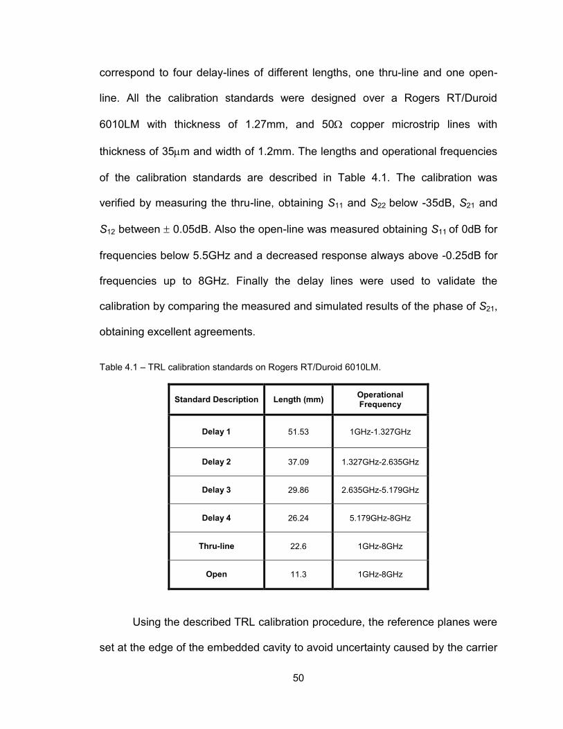
50
correspond to four delay-lines of different lengths, one thru-line and one open-
line. All the calibration standards were designed over a Rogers RT/Duroid
6010LM with thickness of 1.27mm, and 50 copper microstrip lines with
thickness of 35m and width of 1.2mm. The lengths and operational frequencies
of the calibration standards are described in Table 4.1. The calibration was
verified by measuring the thru-line, obtaining S11 and S22 below -35dB, S21 and
S12 between 0.05dB. Also the open-line was measured obtaining S11 of 0dB for
frequencies below 5.5GHz and a decreased response always above -0.25dB for
frequencies up to 8GHz. Finally the delay lines were used to validate the
calibration by comparing the measured and simulated results of the phase of S21,
obtaining excellent agreements.
Table 4.1 – TRL calibration standards on Rogers RT/Duroid 6010LM.
Standard Description Length (mm) Operational Frequency
Delay 1 51.53 1GHz-1.327GHz
Delay 2 37.09 1.327GHz-2.635GHz
Delay 3 29.86 2.635GHz-5.179GHz
Delay 4 26.24 5.179GHz-8GHz
Thru-line 22.6 1GHz-8GHz
Open 11.3 1GHz-8GHz
Using the described TRL calibration procedure, the reference planes were
set at the edge of the embedded cavity to avoid uncertainty caused by the carrier
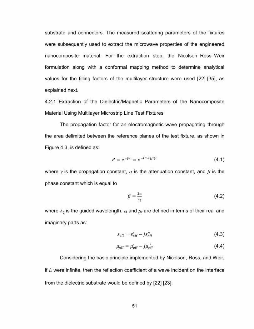
51
substrate and connectors. The measured scattering parameters of the fixtures
were subsequently used to extract the microwave properties of the engineered
nanocomposite material. For the extraction step, the Nicolson–Ross–Weir
formulation along with a conformal mapping method to determine analytical
values for the filling factors of the multilayer structure were used [22]-[35], as
explained next.
4.2.1 Extraction of the Dielectric/Magnetic Parameters of the Nanocomposite
Material Using Multilayer Microstrip Line Test Fixtures
The propagation factor for an electromagnetic wave propagating through
the area delimited between the reference planes of the test fixture, as shown in
Figure 4.3, is defined as:
( (4.1)
where is the propagation constant, is the attenuation constant, and is the
phase constant which is equal to
(4.2)
where g is the guided wavelength. r and r are defined in terms of their real and
imaginary parts as:
(4.3)
(4.4)
Considering the basic principle implemented by Nicolson, Ross, and Weir,
if were infinite, then the reflection coefficient of a wave incident on the interface
from the dielectric substrate would be defined by [22] [23]:
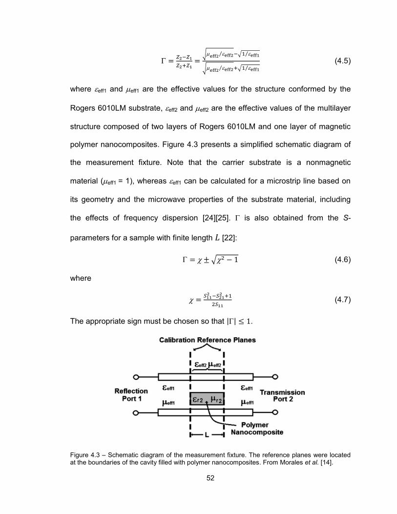
52
√ ⁄ √ ⁄
√ ⁄ √ ⁄ (4.5)
where eff1 and eff1 are the effective values for the structure conformed by the
Rogers 6010LM substrate, eff2 and eff2 are the effective values of the multilayer
structure composed of two layers of Rogers 6010LM and one layer of magnetic
polymer nanocomposites. Figure 4.3 presents a simplified schematic diagram of
the measurement fixture. Note that the carrier substrate is a nonmagnetic
material (eff1 = 1), whereas eff1 can be calculated for a microstrip line based on
its geometry and the microwave properties of the substrate material, including
the effects of frequency dispersion [24][25]. is also obtained from the S-
parameters for a sample with finite length [22]:
√ (4.6)
where
(4.7)
The appropriate sign must be chosen so that || .
Figure 4.3 – Schematic diagram of the measurement fixture. The reference planes were located at the boundaries of the cavity filled with polymer nanocomposites. From Morales et al. [14].
53
The propagation factor can be found from the S–parameters and as
follows [22]:
( (4.8)
Now, from Equation (4.5):
(
)
(4.9)
Complex effective permeability and permittivity can be related to the
propagation constant as [23] :
[
(
)]
(4.10)
where is the frequency in hertz. From Equations (4.9) and (4.10):
√ (4.11)
√
(4.12)
As mentioned by Weir [22], Equation (4.8) is ambiguous and has an
infinite number of roots because the phase of the propagation factor does not
change when the length of the section, that includes the composite material
under test and the Rogers 6010LM, is increased by a multiple of ⁄ . However,
this situation can be resolved by finding the correct roots. The group delay at
each frequency is computed for each solution of eff2 and eff2 by assuming that
their changes are negligible over small increments of frequency [23]
({
[ ( ⁄ ] }
) (4.13)
54
is the group delay in seconds for the th solution of Equations (4.11)
and (4.12). In addition, the measured group delay based on the slope of the
phase of the propagation factor versus frequency can be calculated [23]:
( (
) (4.14)
where is the phase of the propagation factor from Equation (4.8) in radians.
The correct roots, , are selected when the following condition is satisfied
[23]:
| | (4.15)
Using the aforementioned procedure, the equations are algebraically
unstable as , which occurs at frequencies corresponding to integer
multiples of ⁄ . In addition, for small | |, the VNA phase uncertainty is large
and small calibration plane positioning errors can cause large inaccuracies in the
phase [26]. This inaccuracy is significantly bypassed by the implementation
of a two-port calibration in conjunction with the execution of an iterative
algorithm. Discontinuities generated by the instability of the Nicholson–Ross–
Weir method were eliminated and replaced by iteratively calculated values of eff2
and eff2 that satisfy Equations (4.6) to (4.12) with the measured S-parameters
and the consequently derived and values. The solutions derived from the
Nicholson–Ross–Weir method at the starting discrete frequency are used as
initial iterative values, and then the new calculated values are used as the initial
iteration values for the next frequency. A similar procedure is proposed by
Barker-Jarvis et al. [26].
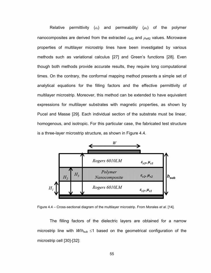
55
Relative permittivity (r) and permeability (r) of the polymer
nanocomposites are derived from the extracted eff2 and eff2 values. Microwave
properties of multilayer microstrip lines have been investigated by various
methods such as variational calculus [27] and Green’s functions [28]. Even
though both methods provide accurate results, they require long computational
times. On the contrary, the conformal mapping method presents a simple set of
analytical equations for the filling factors and the effective permittivity of
multilayer microstrip. Moreover, this method can be extended to have equivalent
expressions for multilayer substrates with magnetic properties, as shown by
Pucel and Masse [29]. Each individual section of the substrate must be linear,
homogenous, and isotropic. For this particular case, the fabricated test structure
is a three-layer microstrip structure, as shown in Figure 4.4.
Figure 4.4 – Cross-sectional diagram of the multilayer microstrip. From Morales et al. [14].
The filling factors of the dielectric layers are obtained for a narrow
microstrip line with W/hsub 1 based on the geometrical configuration of the
microstrip cell [30]-[32]:
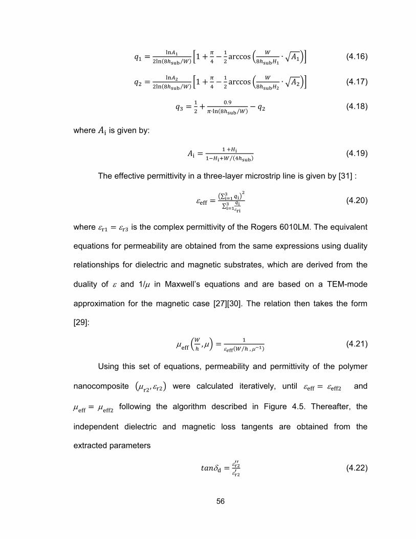
56
( ⁄ [
(
√ )] (4.16)
( ⁄ [
(
√ )] (4.17)
( ⁄ (4.18)
where is given by:
( ⁄ (4.19)
The effective permittivity in a three-layer microstrip line is given by [31] :
(∑
)
∑
(4.20)
where is the complex permittivity of the Rogers 6010LM. The equivalent
equations for permeability are obtained from the same expressions using duality
relationships for dielectric and magnetic substrates, which are derived from the
duality of and 1/ in Maxwell’s equations and are based on a TEM-mode
approximation for the magnetic case [27][30]. The relation then takes the form
[29]:
(
)
( ⁄ (4.21)
Using this set of equations, permeability and permittivity of the polymer
nanocomposite ( ) were calculated iteratively, until and
following the algorithm described in Figure 4.5. Thereafter, the
independent dielectric and magnetic loss tangents are obtained from the
extracted parameters
(4.22)
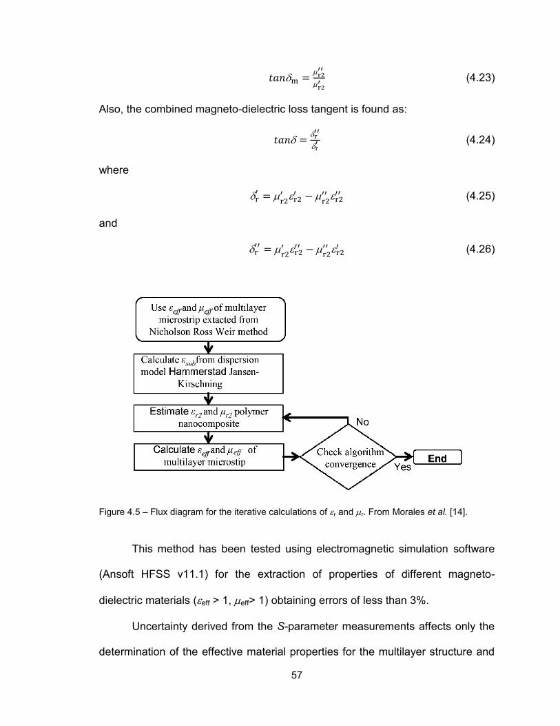
57
(4.23)
Also, the combined magneto-dielectric loss tangent is found as:
(4.24)
where
(4.25)
and
(4.26)
Figure 4.5 – Flux diagram for the iterative calculations of r and r. From Morales et al. [14].
This method has been tested using electromagnetic simulation software
(Ansoft HFSS v11.1) for the extraction of properties of different magneto-
dielectric materials (eff > 1, eff> 1) obtaining errors of less than 3%.
Uncertainty derived from the S-parameter measurements affects only the
determination of the effective material properties for the multilayer structure and
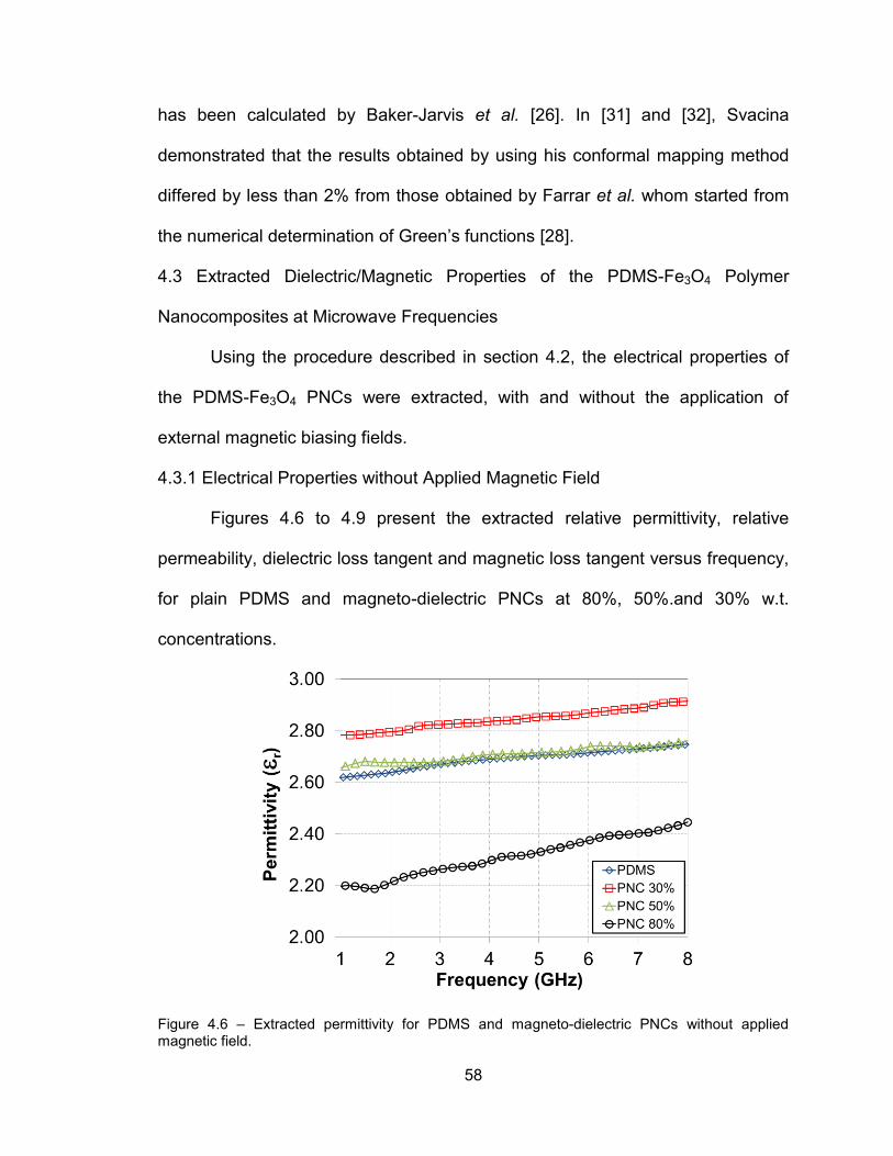
58
has been calculated by Baker-Jarvis et al. [26]. In [31] and [32], Svacina
demonstrated that the results obtained by using his conformal mapping method
differed by less than 2% from those obtained by Farrar et al. whom started from
the numerical determination of Green’s functions [28].
4.3 Extracted Dielectric/Magnetic Properties of the PDMS-Fe3O4 Polymer
Nanocomposites at Microwave Frequencies
Using the procedure described in section 4.2, the electrical properties of
the PDMS-Fe3O4 PNCs were extracted, with and without the application of
external magnetic biasing fields.
4.3.1 Electrical Properties without Applied Magnetic Field
Figures 4.6 to 4.9 present the extracted relative permittivity, relative
permeability, dielectric loss tangent and magnetic loss tangent versus frequency,
for plain PDMS and magneto-dielectric PNCs at 80%, 50%.and 30% w.t.
concentrations.
Figure 4.6 – Extracted permittivity for PDMS and magneto-dielectric PNCs without applied magnetic field.
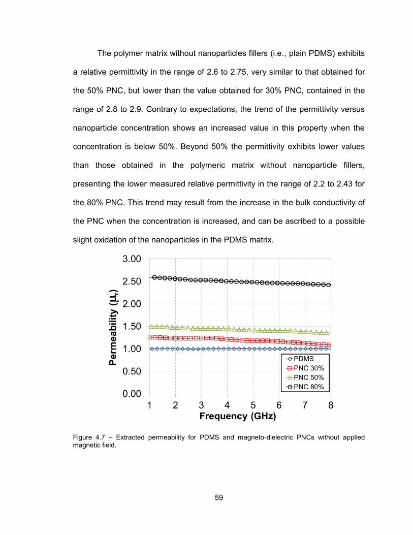
59
The polymer matrix without nanoparticles fillers (i.e., plain PDMS) exhibits
a relative permittivity in the range of 2.6 to 2.75, very similar to that obtained for
the 50% PNC, but lower than the value obtained for 30% PNC, contained in the
range of 2.8 to 2.9. Contrary to expectations, the trend of the permittivity versus
nanoparticle concentration shows an increased value in this property when the
concentration is below 50%. Beyond 50% the permittivity exhibits lower values
than those obtained in the polymeric matrix without nanoparticle fillers,
presenting the lower measured relative permittivity in the range of 2.2 to 2.43 for
the 80% PNC. This trend may result from the increase in the bulk conductivity of
the PNC when the concentration is increased, and can be ascribed to a possible
slight oxidation of the nanoparticles in the PDMS matrix.
Figure 4.7 – Extracted permeability for PDMS and magneto-dielectric PNCs without applied magnetic field.
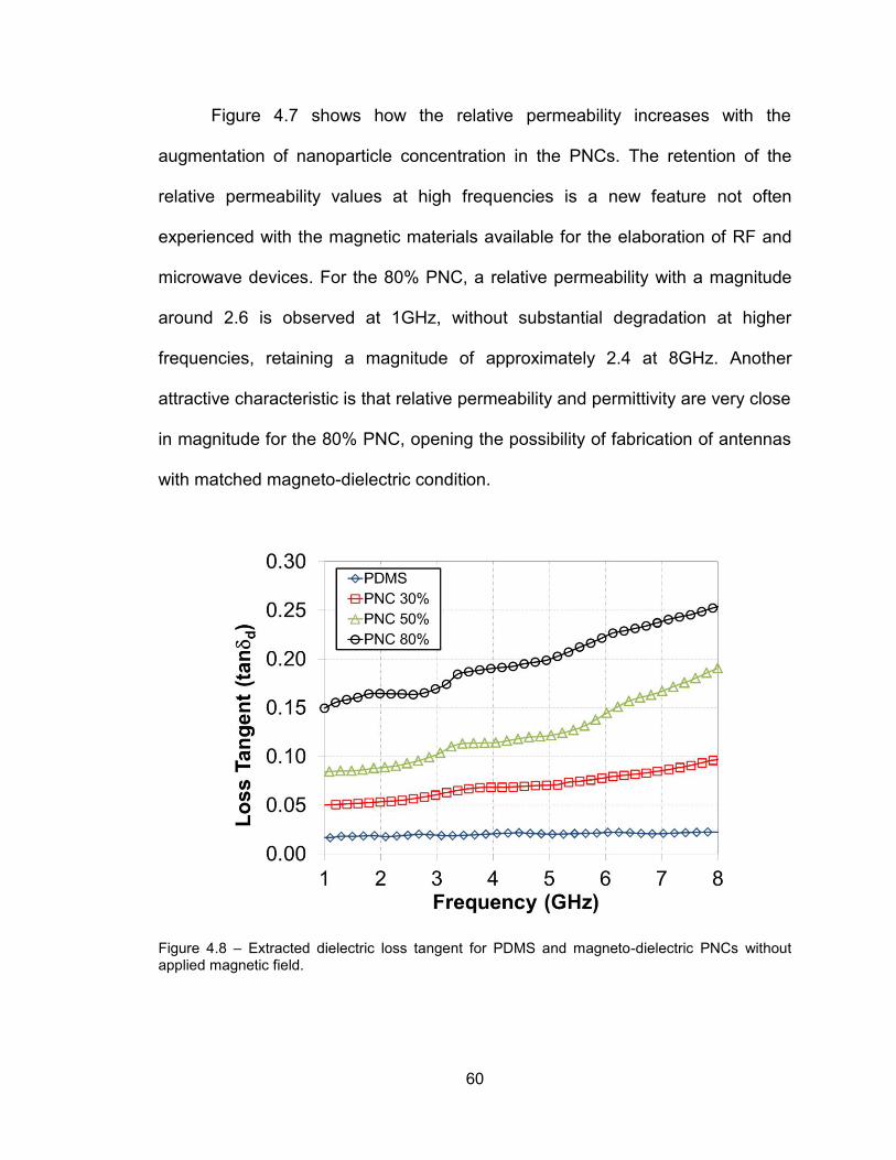
60
Figure 4.7 shows how the relative permeability increases with the
augmentation of nanoparticle concentration in the PNCs. The retention of the
relative permeability values at high frequencies is a new feature not often
experienced with the magnetic materials available for the elaboration of RF and
microwave devices. For the 80% PNC, a relative permeability with a magnitude
around 2.6 is observed at 1GHz, without substantial degradation at higher
frequencies, retaining a magnitude of approximately 2.4 at 8GHz. Another
attractive characteristic is that relative permeability and permittivity are very close
in magnitude for the 80% PNC, opening the possibility of fabrication of antennas
with matched magneto-dielectric condition.
Figure 4.8 – Extracted dielectric loss tangent for PDMS and magneto-dielectric PNCs without applied magnetic field.
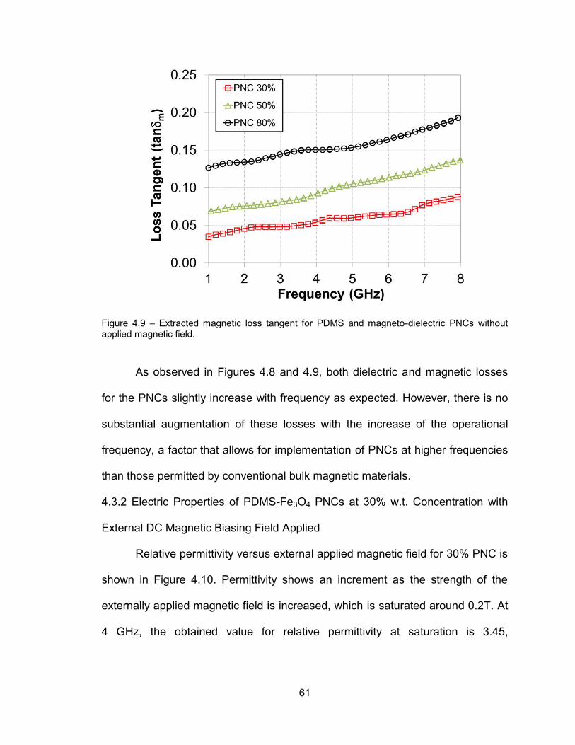
61
Figure 4.9 – Extracted magnetic loss tangent for PDMS and magneto-dielectric PNCs without applied magnetic field.
As observed in Figures 4.8 and 4.9, both dielectric and magnetic losses
for the PNCs slightly increase with frequency as expected. However, there is no
substantial augmentation of these losses with the increase of the operational
frequency, a factor that allows for implementation of PNCs at higher frequencies
than those permitted by conventional bulk magnetic materials.
4.3.2 Electric Properties of PDMS-Fe3O4 PNCs at 30% w.t. Concentration with
External DC Magnetic Biasing Field Applied
Relative permittivity versus external applied magnetic field for 30% PNC is
shown in Figure 4.10. Permittivity shows an increment as the strength of the
externally applied magnetic field is increased, which is saturated around 0.2T. At
4 GHz, the obtained value for relative permittivity at saturation is 3.45,
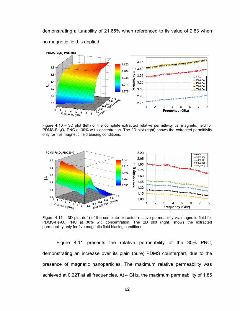
62
demonstrating a tunability of 21.65% when referenced to its value of 2.83 when
no magnetic field is applied.
Figure 4.10 – 3D plot (left) of the complete extracted relative permittivity vs. magnetic field for PDMS-Fe3O4 PNC at 30% w.t. concentration. The 2D plot (right) shows the extracted permittivity only for five magnetic field biasing conditions.
Figure 4.11 – 3D plot (left) of the complete extracted relative permeability vs. magnetic field for PDMS-Fe3O4 PNC at 30% w.t. concentration. The 2D plot (right) shows the extracted permeability only for five magnetic field biasing conditions.
Figure 4.11 presents the relative permeability of the 30% PNC,
demonstrating an increase over its plain (pure) PDMS counterpart, due to the
presence of magnetic nanoparticles. The maximum relative permeability was
achieved at 0.22T at all frequencies. At 4 GHz, the maximum permeability of 1.85
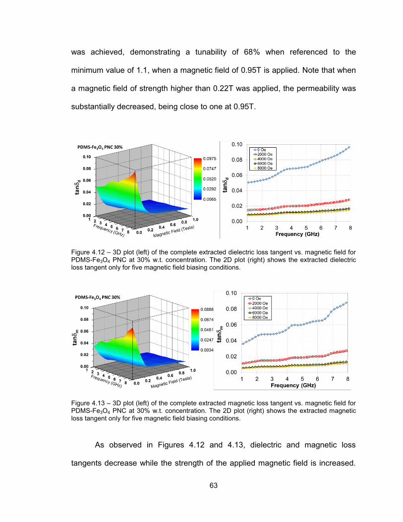
63
was achieved, demonstrating a tunability of 68% when referenced to the
minimum value of 1.1, when a magnetic field of 0.95T is applied. Note that when
a magnetic field of strength higher than 0.22T was applied, the permeability was
substantially decreased, being close to one at 0.95T.
Figure 4.12 – 3D plot (left) of the complete extracted dielectric loss tangent vs. magnetic field for PDMS-Fe3O4 PNC at 30% w.t. concentration. The 2D plot (right) shows the extracted dielectric loss tangent only for five magnetic field biasing conditions.
Figure 4.13 – 3D plot (left) of the complete extracted magnetic loss tangent vs. magnetic field for PDMS-Fe3O4 PNC at 30% w.t. concentration. The 2D plot (right) shows the extracted magnetic loss tangent only for five magnetic field biasing conditions.
As observed in Figures 4.12 and 4.13, dielectric and magnetic loss
tangents decrease while the strength of the applied magnetic field is increased.
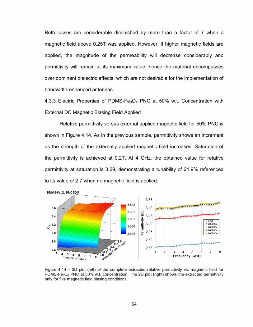
64
Both losses are considerable diminished by more than a factor of 7 when a
magnetic field above 0.25T was applied. However, if higher magnetic fields are
applied, the magnitude of the permeability will decrease considerably and
permittivity will remain at its maximum value, hence the material encompasses
over dominant dielectric effects, which are not desirable for the implementation of
bandwidth-enhanced antennas.
4.3.3 Electric Properties of PDMS-Fe3O4 PNC at 50% w.t. Concentration with
External DC Magnetic Biasing Field Applied
Relative permittivity versus external applied magnetic field for 50% PNC is
shown in Figure 4.14. As in the previous sample, permittivity shows an increment
as the strength of the externally applied magnetic field increases. Saturation of
the permittivity is achieved at 0.2T. At 4 GHz, the obtained value for relative
permittivity at saturation is 3.29, demonstrating a tunability of 21.9% referenced
to its value of 2.7 when no magnetic field is applied.
Figure 4.14 – 3D plot (left) of the complete extracted relative permittivity vs. magnetic field for PDMS-Fe3O4 PNC at 50% w.t. concentration. The 2D plot (right) shows the extracted permittivity only for five magnetic field biasing conditions.
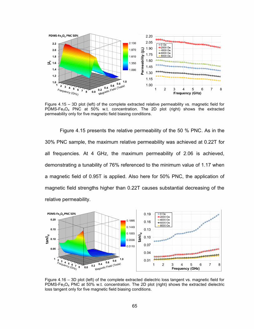
65
Figure 4.15 – 3D plot (left) of the complete extracted relative permeability vs. magnetic field for PDMS-Fe3O4 PNC at 50% w.t. concentration. The 2D plot (right) shows the extracted permeability only for five magnetic field biasing conditions.
Figure 4.15 presents the relative permeability of the 50 % PNC. As in the
30% PNC sample, the maximum relative permeability was achieved at 0.22T for
all frequencies. At 4 GHz, the maximum permeability of 2.06 is achieved,
demonstrating a tunability of 76% referenced to the minimum value of 1.17 when
a magnetic field of 0.95T is applied. Also here for 50% PNC, the application of
magnetic field strengths higher than 0.22T causes substantial decreasing of the
relative permeability.
Figure 4.16 – 3D plot (left) of the complete extracted dielectric loss tangent vs. magnetic field for PDMS-Fe3O4 PNC at 50% w.t. concentration. The 2D plot (right) shows the extracted dielectric loss tangent only for five magnetic field biasing conditions.
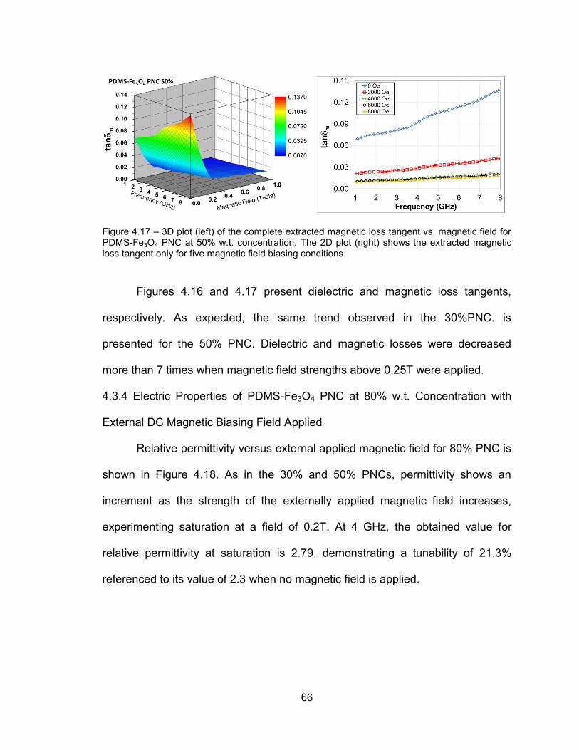
66
Figure 4.17 – 3D plot (left) of the complete extracted magnetic loss tangent vs. magnetic field for PDMS-Fe3O4 PNC at 50% w.t. concentration. The 2D plot (right) shows the extracted magnetic loss tangent only for five magnetic field biasing conditions.
Figures 4.16 and 4.17 present dielectric and magnetic loss tangents,
respectively. As expected, the same trend observed in the 30%PNC. is
presented for the 50% PNC. Dielectric and magnetic losses were decreased
more than 7 times when magnetic field strengths above 0.25T were applied.
4.3.4 Electric Properties of PDMS-Fe3O4 PNC at 80% w.t. Concentration with
External DC Magnetic Biasing Field Applied
Relative permittivity versus external applied magnetic field for 80% PNC is
shown in Figure 4.18. As in the 30% and 50% PNCs, permittivity shows an
increment as the strength of the externally applied magnetic field increases,
experimenting saturation at a field of 0.2T. At 4 GHz, the obtained value for
relative permittivity at saturation is 2.79, demonstrating a tunability of 21.3%
referenced to its value of 2.3 when no magnetic field is applied.
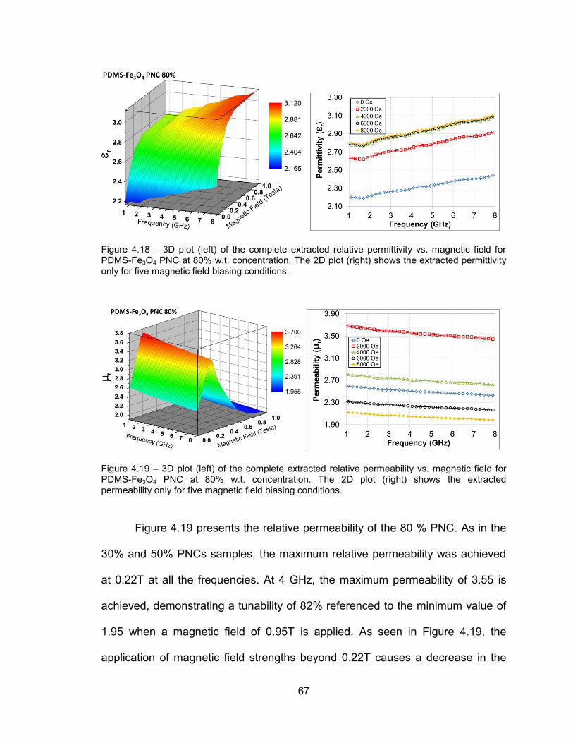
67
Figure 4.18 – 3D plot (left) of the complete extracted relative permittivity vs. magnetic field for PDMS-Fe3O4 PNC at 80% w.t. concentration. The 2D plot (right) shows the extracted permittivity only for five magnetic field biasing conditions.
Figure 4.19 – 3D plot (left) of the complete extracted relative permeability vs. magnetic field for PDMS-Fe3O4 PNC at 80% w.t. concentration. The 2D plot (right) shows the extracted permeability only for five magnetic field biasing conditions.
Figure 4.19 presents the relative permeability of the 80 % PNC. As in the
30% and 50% PNCs samples, the maximum relative permeability was achieved
at 0.22T at all the frequencies. At 4 GHz, the maximum permeability of 3.55 is
achieved, demonstrating a tunability of 82% referenced to the minimum value of
1.95 when a magnetic field of 0.95T is applied. As seen in Figure 4.19, the
application of magnetic field strengths beyond 0.22T causes a decrease in the
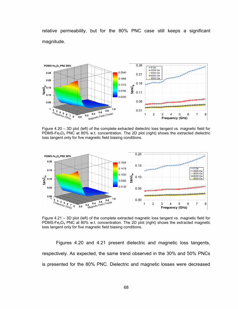
68
relative permeability, but for the 80% PNC case still keeps a significant
magnitude.
Figure 4.20 – 3D plot (left) of the complete extracted dielectric loss tangent vs. magnetic field for PDMS-Fe3O4 PNC at 80% w.t. concentration. The 2D plot (right) shows the extracted dielectric loss tangent only for five magnetic field biasing conditions.
Figure 4.21 – 3D plot (left) of the complete extracted magnetic loss tangent vs. magnetic field for PDMS-Fe3O4 PNC at 80% w.t. concentration. The 2D plot (right) shows the extracted magnetic loss tangent only for five magnetic field biasing conditions.
Figures 4.20 and 4.21 present dielectric and magnetic loss tangents,
respectively. As expected, the same trend observed in the 30% and 50% PNCs
is presented for the 80% PNC. Dielectric and magnetic losses were decreased
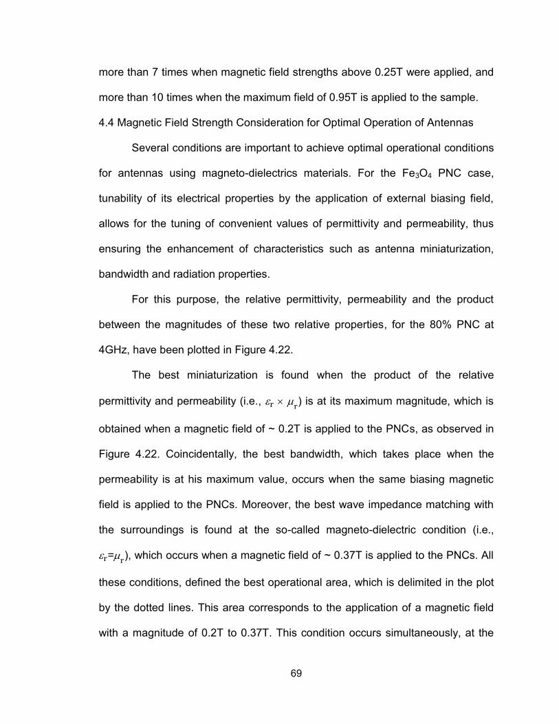
69
more than 7 times when magnetic field strengths above 0.25T were applied, and
more than 10 times when the maximum field of 0.95T is applied to the sample.
4.4 Magnetic Field Strength Consideration for Optimal Operation of Antennas
Several conditions are important to achieve optimal operational conditions
for antennas using magneto-dielectrics materials. For the Fe3O4 PNC case,
tunability of its electrical properties by the application of external biasing field,
allows for the tuning of convenient values of permittivity and permeability, thus
ensuring the enhancement of characteristics such as antenna miniaturization,
bandwidth and radiation properties.
For this purpose, the relative permittivity, permeability and the product
between the magnitudes of these two relative properties, for the 80% PNC at
4GHz, have been plotted in Figure 4.22.
The best miniaturization is found when the product of the relative
permittivity and permeability (i.e., ) is at its maximum magnitude, which is
obtained when a magnetic field of ~ 0.2T is applied to the PNCs, as observed in
Figure 4.22. Coincidentally, the best bandwidth, which takes place when the
permeability is at his maximum value, occurs when the same biasing magnetic
field is applied to the PNCs. Moreover, the best wave impedance matching with
the surroundings is found at the so-called magneto-dielectric condition (i.e.,
= ), which occurs when a magnetic field of ~ 0.37T is applied to the PNCs. All
these conditions, defined the best operational area, which is delimited in the plot
by the dotted lines. This area corresponds to the application of a magnetic field
with a magnitude of 0.2T to 0.37T. This condition occurs simultaneously, at the
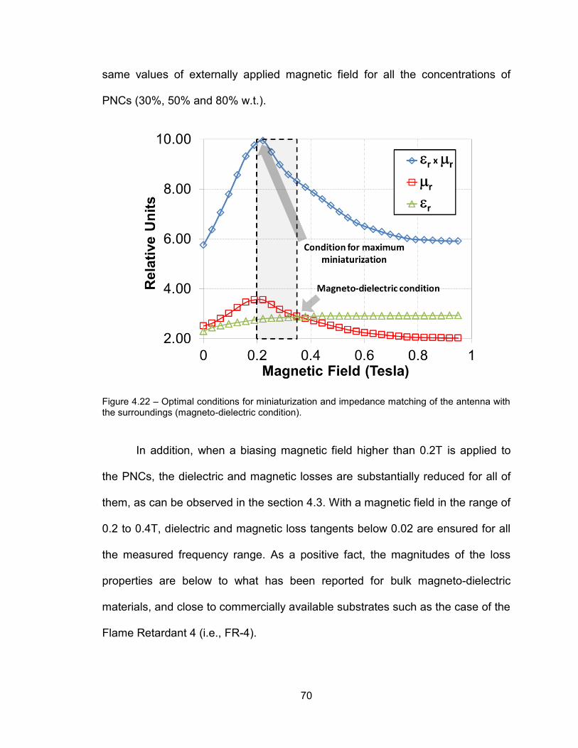
70
same values of externally applied magnetic field for all the concentrations of
PNCs (30%, 50% and 80% w.t.).
Figure 4.22 – Optimal conditions for miniaturization and impedance matching of the antenna with the surroundings (magneto-dielectric condition).
In addition, when a biasing magnetic field higher than 0.2T is applied to
the PNCs, the dielectric and magnetic losses are substantially reduced for all of
them, as can be observed in the section 4.3. With a magnetic field in the range of
0.2 to 0.4T, dielectric and magnetic loss tangents below 0.02 are ensured for all
the measured frequency range. As a positive fact, the magnitudes of the loss
properties are below to what has been reported for bulk magneto-dielectric
materials, and close to commercially available substrates such as the case of the
Flame Retardant 4 (i.e., FR-4).
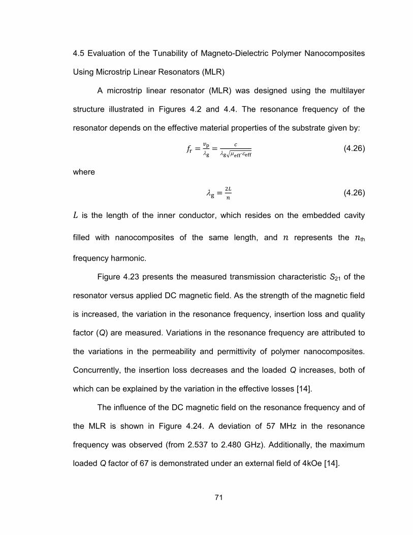
71
4.5 Evaluation of the Tunability of Magneto-Dielectric Polymer Nanocomposites
Using Microstrip Linear Resonators (MLR)
A microstrip linear resonator (MLR) was designed using the multilayer
structure illustrated in Figures 4.2 and 4.4. The resonance frequency of the
resonator depends on the effective material properties of the substrate given by:
√ (4.26)
where
(4.26)
is the length of the inner conductor, which resides on the embedded cavity
filled with nanocomposites of the same length, and represents the th
frequency harmonic.
Figure 4.23 presents the measured transmission characteristic S21 of the
resonator versus applied DC magnetic field. As the strength of the magnetic field
is increased, the variation in the resonance frequency, insertion loss and quality
factor (Q) are measured. Variations in the resonance frequency are attributed to
the variations in the permeability and permittivity of polymer nanocomposites.
Concurrently, the insertion loss decreases and the loaded Q increases, both of
which can be explained by the variation in the effective losses [14].
The influence of the DC magnetic field on the resonance frequency and of
the MLR is shown in Figure 4.24. A deviation of 57 MHz in the resonance
frequency was observed (from 2.537 to 2.480 GHz). Additionally, the maximum
loaded Q factor of 67 is demonstrated under an external field of 4kOe [14].
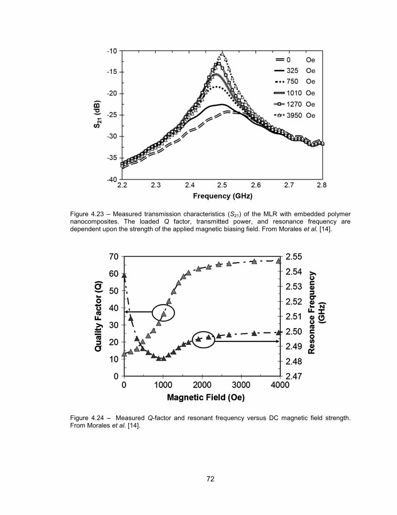
72
Figure 4.23 – Measured transmission characteristics (S21) of the MLR with embedded polymer nanocomposites. The loaded Q factor, transmitted power, and resonance frequency are dependent upon the strength of the applied magnetic biasing field. From Morales et al. [14].
Figure 4.24 – Measured Q-factor and resonant frequency versus DC magnetic field strength. From Morales et al. [14].
73
Chapter 5
Design and Implementation of Multilayer Patch Antennas Using Dielectric and
Magneto-Dielectric Nanocomposite Substrates
5.1 Introduction
In this chapter the fabrication process for multilayer flexible PDMS-based
antennas is presented, followed by description of integration of a magneto-
dielectric nanocomposite substrate. Subsequently, antenna performance is fully
characterized and the results are analyzed based on classical antenna theory.
Four different multilayer microstrip patch antennas have been designed
and fabricated to explore the polymer nanocomposite (PNC) material and its
implementation as a new class of RF/microwave laminates. The first design
consists of a pure Polydimethylsiloxane (PDMS) substrate sandwiched between
two Rogers ULTRALAM® 3850 flexible laminates that contain the copper
metallization layers. The other three designs are constructed on a PDMS
substrate with a cavity completely filled with Fe3O4-PDMS PNC at Fe3O4 loading
concentration of 30%, 50% and 80%, respectively, all of them given by weight
percentage (wt%).
5.2 Design of Multilayer Microstrip Antennas
At first sight, it is very difficult to conceive that given the geometrical
configuration of a microstrip patch antenna, it can operate with minimal
acceptable performance. This reasoning is supported by observing that the
74
radiation is produced by the horizontal electric surface current in a metallization
layer located at a short distance above a ground plane. Based on the predictions
using image theory, such current does not radiate well. However, the patch and
the ground plane together form a resonant cavity which is filled with the substrate
material [36]. Given this characteristic, the microstrip patch antenna has been
selected here because of its high sensitivity to the substrate material properties,
derived from the high interaction within the patch and its ground plane throughout
the substrate.
5.2.1 First Design: Multilayer Patch Antenna on Plain PDMS Substrate
A multilayer patch antenna on pure PDMS substrate has been designed to
operate with a resonant frequency of 4GHz. This frequency has been selected in
order to achieve a dual benefit: a convenient size to optimize the material
resources and to facilitate antenna performance measurements.
In order to retain an attractive radiation efficiency (90%), the thickness of
the substrates has been selected to be around 0.02 (1/50 of the signal
wavelength in free space), as selected in [36] for a Teflon substrate which
exhibits similar electrical characteristics. A thicker substrate selection would lead
to improved radiation efficiency, but requires more substrate material. At 4GHz
( ~74.95mm) a substrate with a thickness of 62mils (1.5748mm) is selected,
which is equivalent to 0.021 .
Figure 5.1 depicts the 3D schematic diagram of the multilayer microstrip
patch antenna assembly and identifies the constituent patterned layers and their
respective thicknesses. As shown, a 60mil (1.524mm) thick PDMS layer is
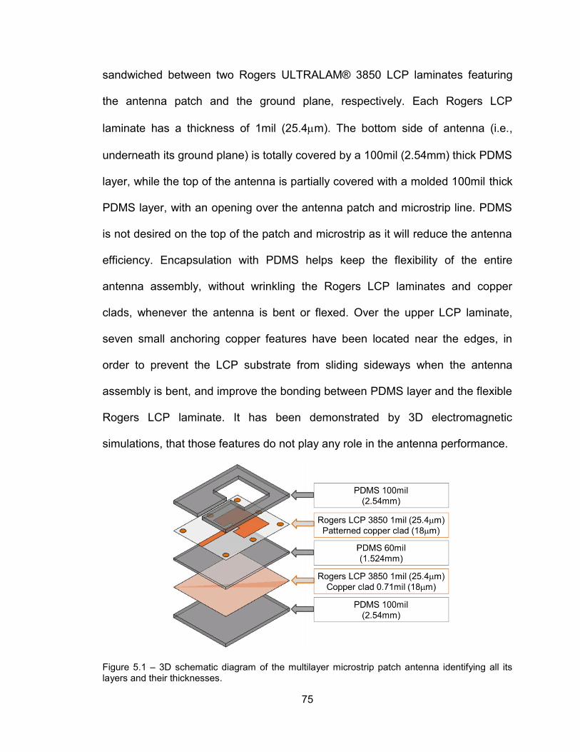
75
sandwiched between two Rogers ULTRALAM® 3850 LCP laminates featuring
the antenna patch and the ground plane, respectively. Each Rogers LCP
laminate has a thickness of 1mil (25.4m). The bottom side of antenna (i.e.,
underneath its ground plane) is totally covered by a 100mil (2.54mm) thick PDMS
layer, while the top of the antenna is partially covered with a molded 100mil thick
PDMS layer, with an opening over the antenna patch and microstrip line. PDMS
is not desired on the top of the patch and microstrip as it will reduce the antenna
efficiency. Encapsulation with PDMS helps keep the flexibility of the entire
antenna assembly, without wrinkling the Rogers LCP laminates and copper
clads, whenever the antenna is bent or flexed. Over the upper LCP laminate,
seven small anchoring copper features have been located near the edges, in
order to prevent the LCP substrate from sliding sideways when the antenna
assembly is bent, and improve the bonding between PDMS layer and the flexible
Rogers LCP laminate. It has been demonstrated by 3D electromagnetic
simulations, that those features do not play any role in the antenna performance.
Figure 5.1 – 3D schematic diagram of the multilayer microstrip patch antenna identifying all its layers and their thicknesses.
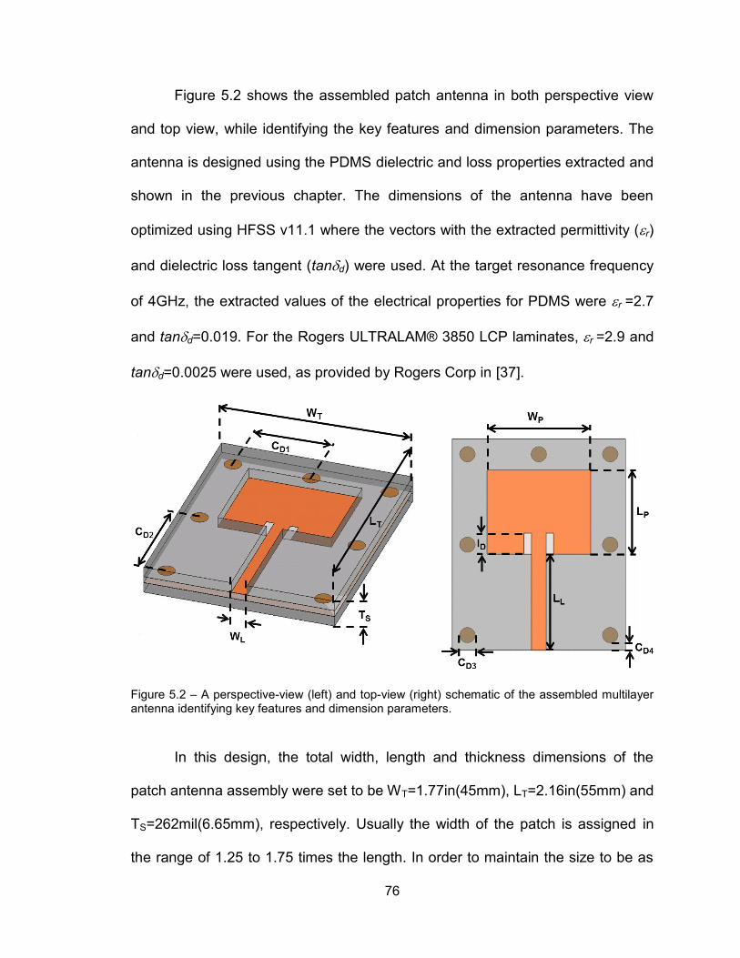
76
Figure 5.2 shows the assembled patch antenna in both perspective view
and top view, while identifying the key features and dimension parameters. The
antenna is designed using the PDMS dielectric and loss properties extracted and
shown in the previous chapter. The dimensions of the antenna have been
optimized using HFSS v11.1 where the vectors with the extracted permittivity (r)
and dielectric loss tangent (tand) were used. At the target resonance frequency
of 4GHz, the extracted values of the electrical properties for PDMS were r =2.7
and tand=0.019. For the Rogers ULTRALAM® 3850 LCP laminates, r =2.9 and
tand=0.0025 were used, as provided by Rogers Corp in [37].
Figure 5.2 – A perspective-view (left) and top-view (right) schematic of the assembled multilayer antenna identifying key features and dimension parameters.
In this design, the total width, length and thickness dimensions of the
patch antenna assembly were set to be WT=1.77in(45mm), LT=2.16in(55mm) and
TS=262mil(6.65mm), respectively. Usually the width of the patch is assigned in
the range of 1.25 to 1.75 times the length. In order to maintain the size to be as
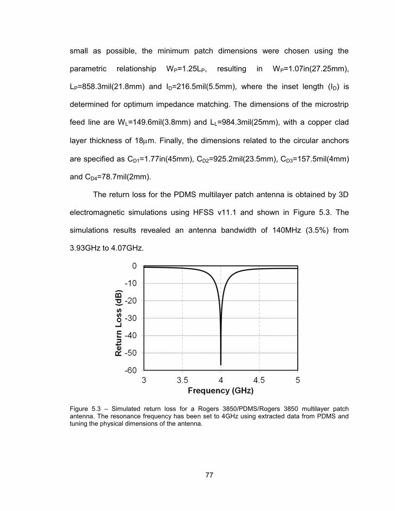
77
small as possible, the minimum patch dimensions were chosen using the
parametric relationship WP=1.25LP, resulting in WP=1.07in(27.25mm),
LP=858.3mil(21.8mm) and ID=216.5mil(5.5mm), where the inset length (ID) is
determined for optimum impedance matching. The dimensions of the microstrip
feed line are WL=149.6mil(3.8mm) and LL=984.3mil(25mm), with a copper clad
layer thickness of 18m. Finally, the dimensions related to the circular anchors
are specified as CD1=1.77in(45mm), CD2=925.2mil(23.5mm), CD3=157.5mil(4mm)
and CD4=78.7mil(2mm).
The return loss for the PDMS multilayer patch antenna is obtained by 3D
electromagnetic simulations using HFSS v11.1 and shown in Figure 5.3. The
simulations results revealed an antenna bandwidth of 140MHz (3.5%) from
3.93GHz to 4.07GHz.
Figure 5.3 – Simulated return loss for a Rogers 3850/PDMS/Rogers 3850 multilayer patch antenna. The resonance frequency has been set to 4GHz using extracted data from PDMS and tuning the physical dimensions of the antenna.
78
5.2.2 Second Design: Multilayer Patch Antenna on PDMS-Fe3O4 PNC Substrate
A modified version of the multilayer patch antenna with PDMS-Fe3O4 PNC
substrate is presented herein. For ease of comparison, this antenna has also
been set to work with a resonance frequency of 4GHz. Figure 5.4 presents the
3D schematic diagram of the multilayer microstrip patch antenna assembly while
identifying all its layers and their respective thicknesses. As seen, this design
differs from the previous in the incorporation of the PDMS-Fe3O4 PNC
underneath the patch and between the two Rogers ULTRALAM® 3850 LCP
laminates. Also, dimensions of the patch have been adjusted from those in the
previous design to retain the same resonance frequency. Figure 5.5 shows the
physical dimensions of the new antenna design. Now, WP=777.56mil(19.75mm),
LP=622.05mil(15.8mm) and the insets are no longer needed (ID=0). In addition,
the dimensions of the PDMS-Fe3O4 PNC filled cavity are WN=866.14mil(22mm),
LN=669.29mil(17mm) and with the same thickness of the PDMS substrate
60mil(1.524mm). The rest of the physical parameters are kept the same as in the
previous design. As noted, since the resonance frequency of the antenna has
been kept the same, then size comparison between the antennas could be
accomplished based on the areas of the antenna patch in different designs.
79
Figure 5.4 – 3D schematic of the multilayer microstrip patch antenna with a cavity embedded completely filled with PDMS-Fe3O4 PNC. The composition and thickness for each layer is also clearly specified.
Figure 5.5 – A perspective-view (left) and top-view (right) schematic of the assembled multilayer antenna, which includes a PDMS-Fe3O4 PNC filled cavity underneath the antenna patch. Both figures identify key features and dimension parameters. Note that WN and LN describe the dimensions of the embedded PNC layer.
80
Figure 5.6 – Simulated return loss for the multilayer patch antenna with embedded PDMS-Fe3O4 nanocomposite and 80% w.t. loading. The resonance frequency has been set to 4GHz using extracted data from PDMS-Fe3O4 PNC at this concentration, and tuning the physical dimensions of the antenna.
The simulated return loss for the PDMS multilayer patch antenna with
embedded 80% PDMS-Fe3O4 nanocomposites is shown in Figure 5.6. The
multilayer antenna exhibited a bandwidth of 1.081GHz (27%) from 3.479GHz to
4.560GHz.
5.3 Fabrication of Multilayer Microstrip Patch Antennas
To assemble the multilayer antenna, the two Roger LCP flexible laminates
and the PDMS layers have been patterned using standard photolithography
processes and deposited in-house molding techniques, respectively. For the
sake of brevity and better organization, the entire fabrication process has been
divided into two different subsections. The first one describes the step-by-step
processes for fabrication of a multilayer patch antenna on a PDMS substrate.
The second one describes the fabrication of the multilayer antenna on a PDMS
81
substrate with an embedded cavity filled with PDMS-Fe3O4 PNC underneath the
antenna patch.
5.3.1 Fabrication of Multilayer Patch Antennas on PDMS Substrate
One mil (25.4m) thick flexible Rogers ULTRALAM® 3850 LCP laminates
are used to form the patterned metallization layers (i.e., patch, microstrip feed
line and ground plane) of the multilayer patch antenna. Figure 5.7 shows the
process flow followed for definition of the ground plane used in the multilayer
microstrip antenna assembly. Initially, one of the copper clads is protected by a
layer of negative dry film photoresist (416DFR from MG Chemicals). This
photoresist is then exposed to UV-light for 2 minutes using a Kinsten KVB30D-
AU UV exposure box. Subsequently, the substrate is submerged in ferric chloride
solution in a Kinsten ET20 etching tank at 60C with bubble agitation for 8
minutes, followed by rinsing in DI water. The copper clad over the unprotected
side is completely removed, while the side protected by the dry film remains
unaltered. Finally, the remaining photoresist is stripped away by submerging the
substrate in acetone for 3 minutes followed by DI water rinsing until any other
chemical residue is removed. As the process described herein involves the use
of photosensitive dry film, the entire process step is carried out in a cleanroom
facility under “yellow light”.
82
Figure 5.7 – Cross-sectional view diagram of the fabrication process flow for patterning the ground plane on one side of a Rogers LCP 3850 laminate.
As seen in Figure 5.8, for patterning the antenna patch and the microstrip
feed line, a similar procedure was followed with addition of one more step. One
side of the Rogers LCP 3850 laminate was covered with the dry film photoresist,
and exposed to UV-light for 2 minutes through a photo mask in an acetate
transparency. The transparency photo-mask for definition of the antenna patch
and microstrip feed line was designed using Autodesk AutoCAD, and printed out
by an Epson stylish 3800 inkjet printer onto HP premium inkjet transparency film
sheets (C3834A). After exposure under UV light for 2 minutes, the negative dry
film photoresist was developed for 5 minutes in Negative Photoresist Developer
(4170 from MG Chemicals) dissolved in water in a 1:10 ratio. After the
development step, the portion of the copper clad for the antenna patch and
feedline was protected by the negative photoresist, whereas the exposed copper
(including the entire copper clad on the back of the substrate) was removed by
ferric chloride copper etchant solution. Finally, the photoresist was stripped using
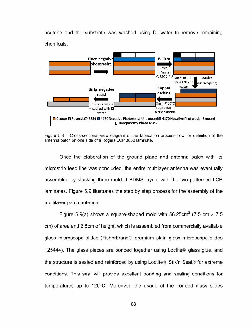
83
acetone and the substrate was washed using DI water to remove remaining
chemicals.
Figure 5.8 – Cross-sectional view diagram of the fabrication process flow for definition of the antenna patch on one side of a Rogers LCP 3850 laminate.
Once the elaboration of the ground plane and antenna patch with its
microstrip feed line was concluded, the entire multilayer antenna was eventually
assembled by stacking three molded PDMS layers with the two patterned LCP
laminates. Figure 5.9 illustrates the step by step process for the assembly of the
multilayer patch antenna.
Figure 5.9(a) shows a square-shaped mold with 56.25cm2 (7.5 cm 7.5
cm) of area and 2.5cm of height, which is assembled from commercially available
glass microscope slides (Fisherbrand premium plain glass microscope slides
125444). The glass pieces are bonded together using Loctite glass glue, and
the structure is sealed and reinforced by using Loctite Stik’n Seal for extreme
conditions. This seal will provide excellent bonding and sealing conditions for
temperatures up to 120C. Moreover, the usage of the bonded glass slides
84
system facilitates the casting and de-molding of the PDMS layer as these can be
easily detached by bending the structure.
The base resin and curing agents of Sylgard 184 are mixed in a 10:1
weight ratio. PDMS (Sylgard 184) has a specific gravity of 1.03 at room
temperature. Initially a layer with 100mil (0.254cm) of thickness is deposited. For
this purpose, the following basic equations are used:
(5.1)
(5.2)
where VS and TS are the volume and desired thickness of the deposited layer
respectively, AM is the area of the mold equivalent to 56.25cm2, WPDMS is the
required PDMS mass to achieve the desired layer thickness and PDMS is the
density of PDMS which is 1.03g/cm3.
Using the pre-designed mold and equations 5.1 and 5.2, a volume VS of
14.2875cm3 is required for a desired thickness TS of 100mil (2.54mm), which
results in required PDMS mass WPDMS of 14.7161g.
The mold is placed in an single pan electronic balance (Mettler AE100)
and (14.7161+0.48)g of PDMS are poured into the mold. From several
experiments, it has been found that an additional PDMS mass of 0.48g is needed
to achieve the desired thickness given the amount of residual polymer material
adhered to the walls of the mold (meniscus formation).
In a convection vacuum oven (Fisher 281A), 30inHg of vacuum are
applied for 5 minutes to extract the trapped air bubbles in the PDMS.
Subsequently the polymer is cured by heating to 90C for 45 minutes. The mold
85
is extracted from the oven and cooled down to room temperature, resulting in the
structure shown in Figure 5.9(b). From previous experiments, the thickness of the
PDMS layer has been measured by using a caliper obtaining a reading of
2.550.08mm, which is equivalent to a standard deviation of less than 3.2%.
Thereafter, the ground plane of dimension 55mm 45mm, patterned on a
Rogers ULTRALAM® 3850 LCP laminate, is placed at the center of the mold
(Figure 5.9(c)). The LCP laminate and PDMS layer were stuck together
spontaneously under vacuum, which also helps avoid bubble formation within
their interface.
Subsequently, a 60mil (1.524mm) thick PDMS layer is molded with total
amount of PDMS determined by Equations (5.1) and (5.2). (8.83+0.48)g of
PDMS are poured into the mold, and placed under 30inHg of vacuum for 5
minutes to remove air trapped bubbles. Finally, the PDMS is cured by heating the
sample to 90C for 45 minutes (Figure 5.9(d)). Once the sample is cured and
cooled down to room temperature, the Rogers ULTRALAM® 3850 LCP laminate
with patterned antenna patch is positioned at the center of the mold as shown in
Figure 5.9(e). The LCP laminate sticks to the surface of the molded PDMS
spontaneously. In order to remove the PDMS that will be deposited on top of the
antenna, acetate transparency is placed on top of the patch and microstrip line
using double-sided adhesive tape, which will be removed after the curing
process. 30mmHg of vacuum are applied to remove trapped air bubbles at the
interfaces between the two layers. Then the sample is removed from vacuum
and (14.7161+0.48)g of PDMS are poured in the mold to form a 100mil(2.54mm)
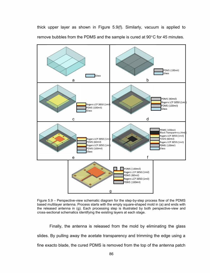
86
thick upper layer as shown in Figure 5.9(f). Similarly, vacuum is applied to
remove bubbles from the PDMS and the sample is cured at 90C for 45 minutes.
a
b
c
d
e
f
g
Figure 5.9 – Perspective-view schematic diagram for the step-by-step process flow of the PDMS based multilayer antenna. Process starts with the empty square-shaped mold in (a) and ends with the released antenna in (g). Each processing step is illustrated by both perspective-view and cross-sectional schematics identifying the existing layers at each stage.
Finally, the antenna is released from the mold by eliminating the glass
slides. By pulling away the acetate transparency and trimming the edge using a
fine exacto blade, the cured PDMS is removed from the top of the antenna patch
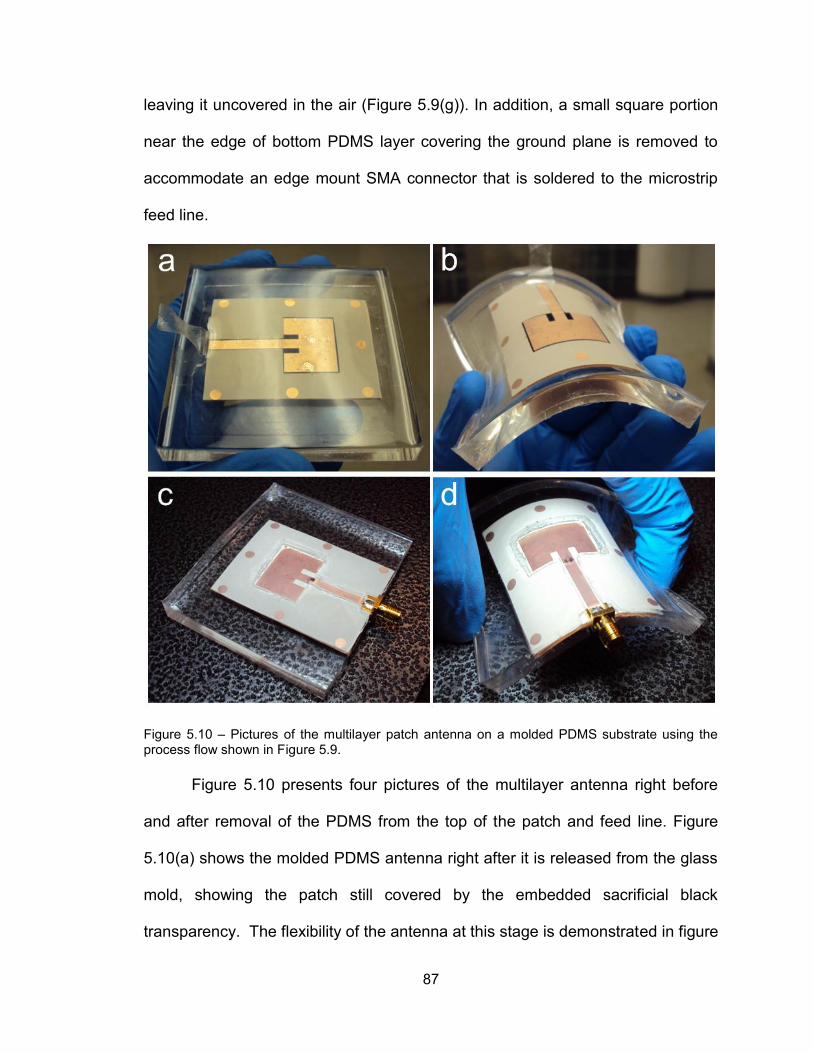
87
leaving it uncovered in the air (Figure 5.9(g)). In addition, a small square portion
near the edge of bottom PDMS layer covering the ground plane is removed to
accommodate an edge mount SMA connector that is soldered to the microstrip
feed line.
Figure 5.10 – Pictures of the multilayer patch antenna on a molded PDMS substrate using the process flow shown in Figure 5.9.
Figure 5.10 presents four pictures of the multilayer antenna right before
and after removal of the PDMS from the top of the patch and feed line. Figure
5.10(a) shows the molded PDMS antenna right after it is released from the glass
mold, showing the patch still covered by the embedded sacrificial black
transparency. The flexibility of the antenna at this stage is demonstrated in figure
88
5.10(b), which also verifies no wrinkle formation in the antenna after bending.
The final multilayer antenna right after removal of the embedded sacrificial
transparency, to fully expose the antenna patch and feed line, is presented in
figure 5.10(c). In addition, the antenna feed line and port has been terminated
with a coaxial SMA connector. Finally, the completed antenna with SMA
connected is bent to demonstrate its flexibility (figure 5.10(d)).
5.3.2 Multilayer Patch Antenna on Hybrid PDMS/Fe3O4-PDMS Substrate
For this design, both metallization layers (ground plane and patch) are
constructed on Rogers LCP 3850 flexible laminates following the same process
steps as shown in Figure 5.8. As a layer of PDMS-Fe3O4 PNC is incorporated in
this design, the fabrication process of the multilayer array is modified to facilitate
the integration of the new layer. Figure 5.11 shows the new process used for the
construction of the multilayer patch antenna on a hybrid PDMS/Fe3O4-PDMS
substrate.
As shown in Figure 5.11(a), the process starts with a custom-built glass
mold identical to that used in the previous design. As detailed in the previous
section, the multilayer antenna is constructed starting from the bottom side up,
inside the mold. The first two layers including the first PDMS layer and the first
LCP laminate with patterned ground plane are kept the same as depicted in
Figures 5.11(b) and 5.11(c). The third layer (from the bottom up) is a 60mil thick
PDMS layer with an embedded cavity filled with PDMS-Fe3O4 PNC, which is
molded separately and machined by a LPKF ProtoMat S62 milling machine.
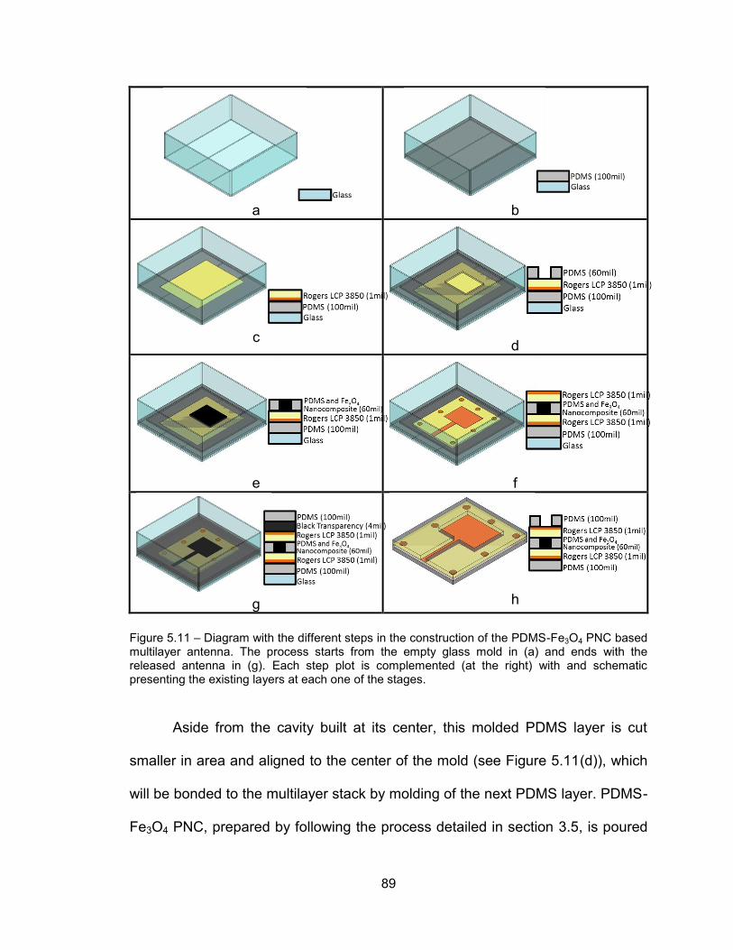
89
a
b
c
d
e
f
g
h
Figure 5.11 – Diagram with the different steps in the construction of the PDMS-Fe3O4 PNC based multilayer antenna. The process starts from the empty glass mold in (a) and ends with the released antenna in (g). Each step plot is complemented (at the right) with and schematic presenting the existing layers at each one of the stages.
Aside from the cavity built at its center, this molded PDMS layer is cut
smaller in area and aligned to the center of the mold (see Figure 5.11(d)), which
will be bonded to the multilayer stack by molding of the next PDMS layer. PDMS-
Fe3O4 PNC, prepared by following the process detailed in section 3.5, is poured
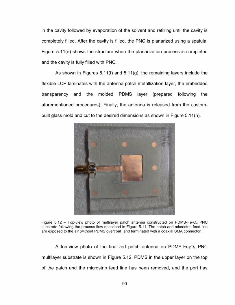
90
in the cavity followed by evaporation of the solvent and refilling until the cavity is
completely filled. After the cavity is filled, the PNC is planarized using a spatula.
Figure 5.11(e) shows the structure when the planarization process is completed
and the cavity is fully filled with PNC.
As shown in Figures 5.11(f) and 5.11(g), the remaining layers include the
flexible LCP laminates with the antenna patch metallization layer, the embedded
transparency and the molded PDMS layer (prepared following the
aforementioned procedures). Finally, the antenna is released from the custom-
built glass mold and cut to the desired dimensions as shown in Figure 5.11(h).
Figure 5.12 – Top-view photo of multilayer patch antenna constructed on PDMS-Fe3O4 PNC substrate following the process flow described in Figure 5.11. The patch and microstrip feed line are exposed to the air (without PDMS overcoat) and terminated with a coaxial SMA connector.
A top-view photo of the finalized patch antenna on PDMS-Fe3O4 PNC
multilayer substrate is shown in Figure 5.12. PDMS in the upper layer on the top
of the patch and the microstrip feed line has been removed, and the port has
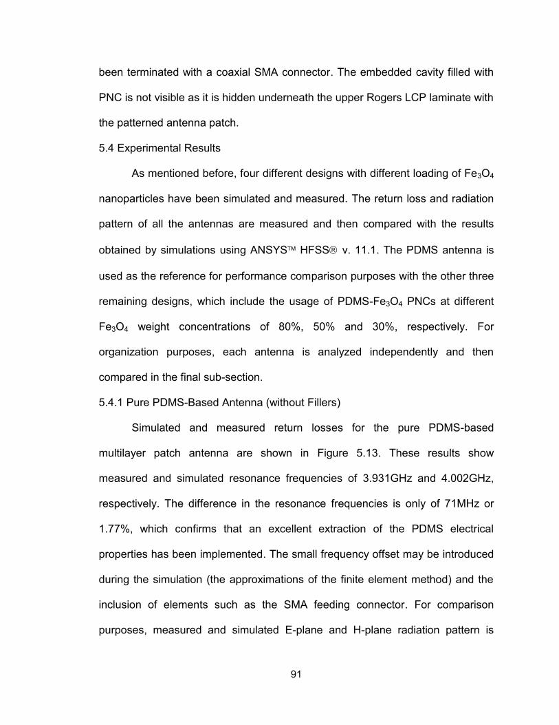
91
been terminated with a coaxial SMA connector. The embedded cavity filled with
PNC is not visible as it is hidden underneath the upper Rogers LCP laminate with
the patterned antenna patch.
5.4 Experimental Results
As mentioned before, four different designs with different loading of Fe3O4
nanoparticles have been simulated and measured. The return loss and radiation
pattern of all the antennas are measured and then compared with the results
obtained by simulations using ANSYS HFSS v. 11.1. The PDMS antenna is
used as the reference for performance comparison purposes with the other three
remaining designs, which include the usage of PDMS-Fe3O4 PNCs at different
Fe3O4 weight concentrations of 80%, 50% and 30%, respectively. For
organization purposes, each antenna is analyzed independently and then
compared in the final sub-section.
5.4.1 Pure PDMS-Based Antenna (without Fillers)
Simulated and measured return losses for the pure PDMS-based
multilayer patch antenna are shown in Figure 5.13. These results show
measured and simulated resonance frequencies of 3.931GHz and 4.002GHz,
respectively. The difference in the resonance frequencies is only of 71MHz or
1.77%, which confirms that an excellent extraction of the PDMS electrical
properties has been implemented. The small frequency offset may be introduced
during the simulation (the approximations of the finite element method) and the
inclusion of elements such as the SMA feeding connector. For comparison
purposes, measured and simulated E-plane and H-plane radiation pattern is
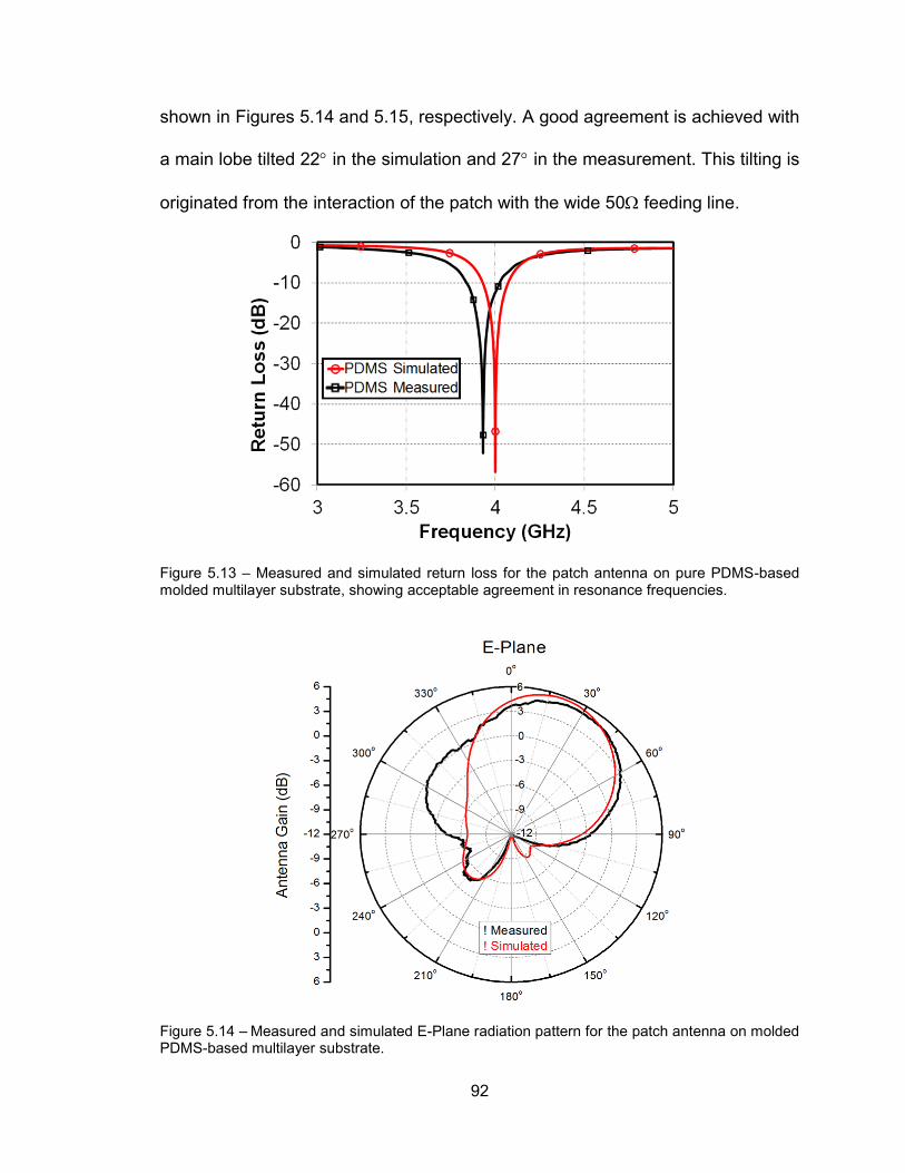
92
shown in Figures 5.14 and 5.15, respectively. A good agreement is achieved with
a main lobe tilted 22 in the simulation and 27 in the measurement. This tilting is
originated from the interaction of the patch with the wide 50 feeding line.
Figure 5.13 – Measured and simulated return loss for the patch antenna on pure PDMS-based molded multilayer substrate, showing acceptable agreement in resonance frequencies.
Figure 5.14 – Measured and simulated E-Plane radiation pattern for the patch antenna on molded PDMS-based multilayer substrate.
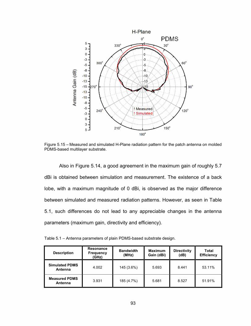
93
Figure 5.15 – Measured and simulated H-Plane radiation pattern for the patch antenna on molded PDMS-based multilayer substrate.
Also in Figure 5.14, a good agreement in the maximum gain of roughly 5.7
dBi is obtained between simulation and measurement. The existence of a back
lobe, with a maximum magnitude of 0 dBi, is observed as the major difference
between simulated and measured radiation patterns. However, as seen in Table
5.1, such differences do not lead to any appreciable changes in the antenna
parameters (maximum gain, directivity and efficiency).
Table 5.1 – Antenna parameters of plain PDMS-based substrate design.
Description Resonance Frequency
(GHz) Bandwidth
(MHz) Maximum Gain (dBi)
Directivity (dB)
Total Efficiency
Simulated PDMS Antenna 4.002 145 (3.6%) 5.693 8.441 53.11%
Measured PDMS Antenna 3.931 185 (4.7%) 5.681 8.527 51.91%
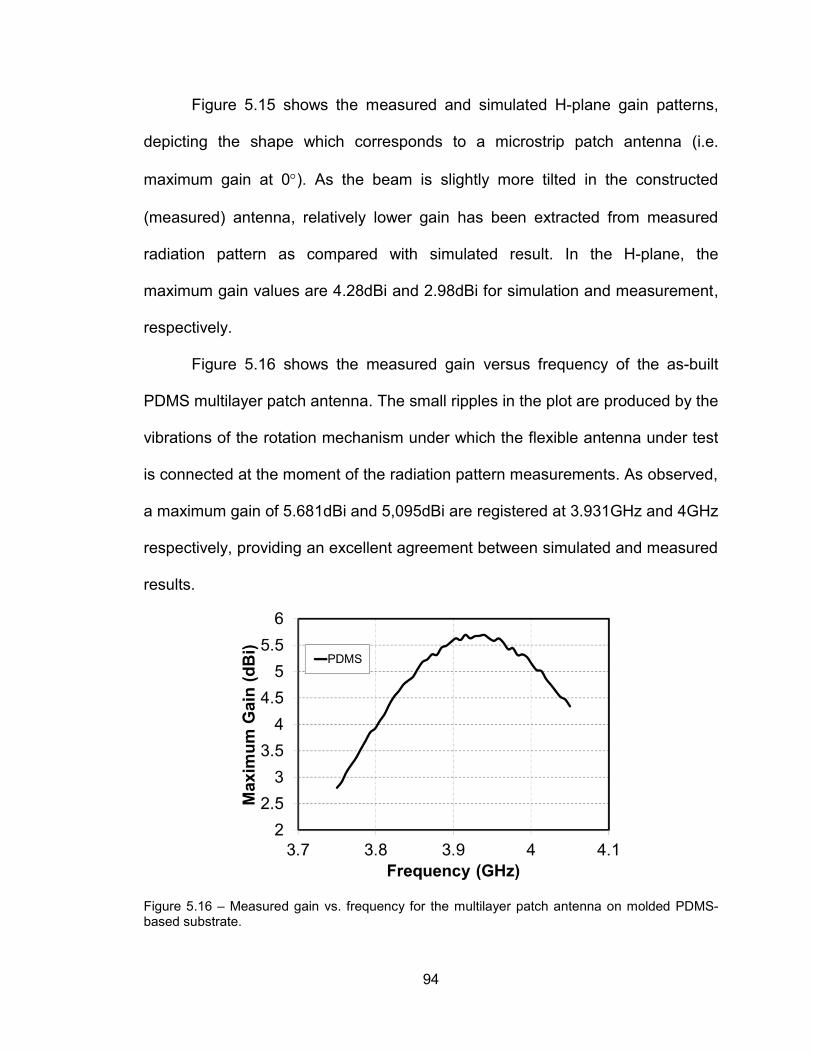
94
Figure 5.15 shows the measured and simulated H-plane gain patterns,
depicting the shape which corresponds to a microstrip patch antenna (i.e.
maximum gain at 0). As the beam is slightly more tilted in the constructed
(measured) antenna, relatively lower gain has been extracted from measured
radiation pattern as compared with simulated result. In the H-plane, the
maximum gain values are 4.28dBi and 2.98dBi for simulation and measurement,
respectively.
Figure 5.16 shows the measured gain versus frequency of the as-built
PDMS multilayer patch antenna. The small ripples in the plot are produced by the
vibrations of the rotation mechanism under which the flexible antenna under test
is connected at the moment of the radiation pattern measurements. As observed,
a maximum gain of 5.681dBi and 5,095dBi are registered at 3.931GHz and 4GHz
respectively, providing an excellent agreement between simulated and measured
results.
Figure 5.16 – Measured gain vs. frequency for the multilayer patch antenna on molded PDMS-based substrate.
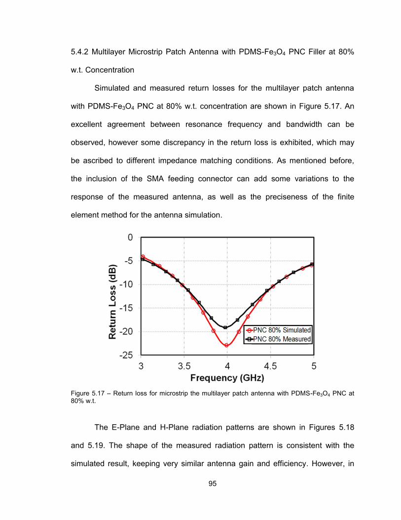
95
5.4.2 Multilayer Microstrip Patch Antenna with PDMS-Fe3O4 PNC Filler at 80%
w.t. Concentration
Simulated and measured return losses for the multilayer patch antenna
with PDMS-Fe3O4 PNC at 80% w.t. concentration are shown in Figure 5.17. An
excellent agreement between resonance frequency and bandwidth can be
observed, however some discrepancy in the return loss is exhibited, which may
be ascribed to different impedance matching conditions. As mentioned before,
the inclusion of the SMA feeding connector can add some variations to the
response of the measured antenna, as well as the preciseness of the finite
element method for the antenna simulation.
Figure 5.17 – Return loss for microstrip the multilayer patch antenna with PDMS-Fe3O4 PNC at 80% w.t.
The E-Plane and H-Plane radiation patterns are shown in Figures 5.18
and 5.19. The shape of the measured radiation pattern is consistent with the
simulated result, keeping very similar antenna gain and efficiency. However, in
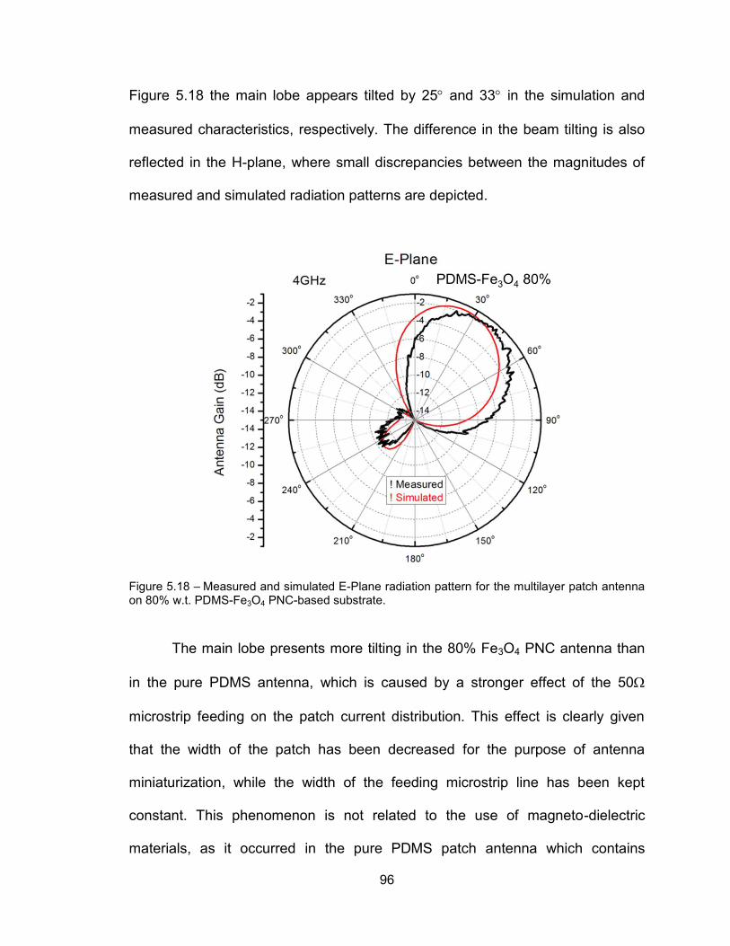
96
Figure 5.18 the main lobe appears tilted by 25 and 33 in the simulation and
measured characteristics, respectively. The difference in the beam tilting is also
reflected in the H-plane, where small discrepancies between the magnitudes of
measured and simulated radiation patterns are depicted.
Figure 5.18 – Measured and simulated E-Plane radiation pattern for the multilayer patch antenna on 80% w.t. PDMS-Fe3O4 PNC-based substrate.
The main lobe presents more tilting in the 80% Fe3O4 PNC antenna than
in the pure PDMS antenna, which is caused by a stronger effect of the 50
microstrip feeding on the patch current distribution. This effect is clearly given
that the width of the patch has been decreased for the purpose of antenna
miniaturization, while the width of the feeding microstrip line has been kept
constant. This phenomenon is not related to the use of magneto-dielectric
materials, as it occurred in the pure PDMS patch antenna which contains
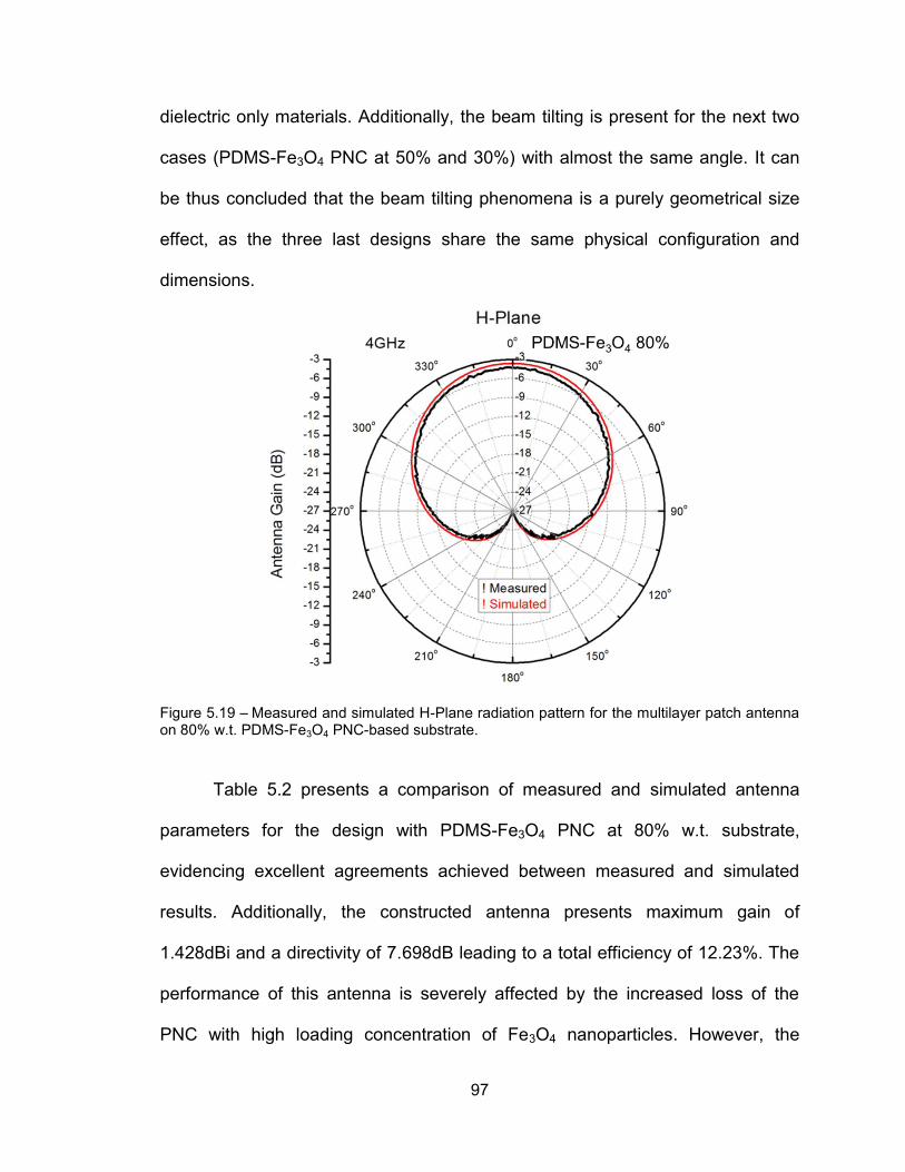
97
dielectric only materials. Additionally, the beam tilting is present for the next two
cases (PDMS-Fe3O4 PNC at 50% and 30%) with almost the same angle. It can
be thus concluded that the beam tilting phenomena is a purely geometrical size
effect, as the three last designs share the same physical configuration and
dimensions.
Figure 5.19 – Measured and simulated H-Plane radiation pattern for the multilayer patch antenna on 80% w.t. PDMS-Fe3O4 PNC-based substrate.
Table 5.2 presents a comparison of measured and simulated antenna
parameters for the design with PDMS-Fe3O4 PNC at 80% w.t. substrate,
evidencing excellent agreements achieved between measured and simulated
results. Additionally, the constructed antenna presents maximum gain of
1.428dBi and a directivity of 7.698dB leading to a total efficiency of 12.23%. The
performance of this antenna is severely affected by the increased loss of the
PNC with high loading concentration of Fe3O4 nanoparticles. However, the
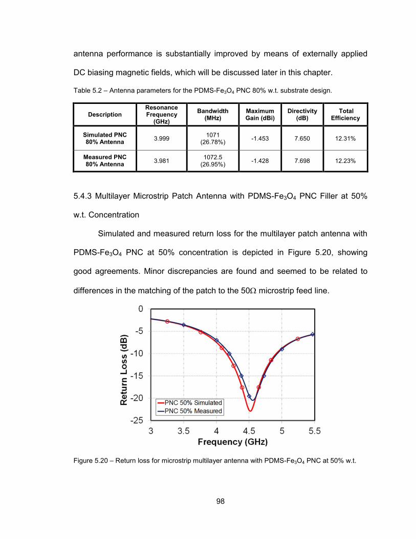
98
antenna performance is substantially improved by means of externally applied
DC biasing magnetic fields, which will be discussed later in this chapter.
Table 5.2 – Antenna parameters for the PDMS-Fe3O4 PNC 80% w.t. substrate design.
Description Resonance Frequency
(GHz) Bandwidth
(MHz) Maximum Gain (dBi)
Directivity (dB)
Total Efficiency
Simulated PNC 80% Antenna 3.999 1071
(26.78%) -1.453 7.650 12.31%
Measured PNC 80% Antenna 3.981 1072.5
(26.95%) -1.428 7.698 12.23%
5.4.3 Multilayer Microstrip Patch Antenna with PDMS-Fe3O4 PNC Filler at 50%
w.t. Concentration
Simulated and measured return loss for the multilayer patch antenna with
PDMS-Fe3O4 PNC at 50% concentration is depicted in Figure 5.20, showing
good agreements. Minor discrepancies are found and seemed to be related to
differences in the matching of the patch to the 50 microstrip feed line.
Figure 5.20 – Return loss for microstrip multilayer antenna with PDMS-Fe3O4 PNC at 50% w.t.
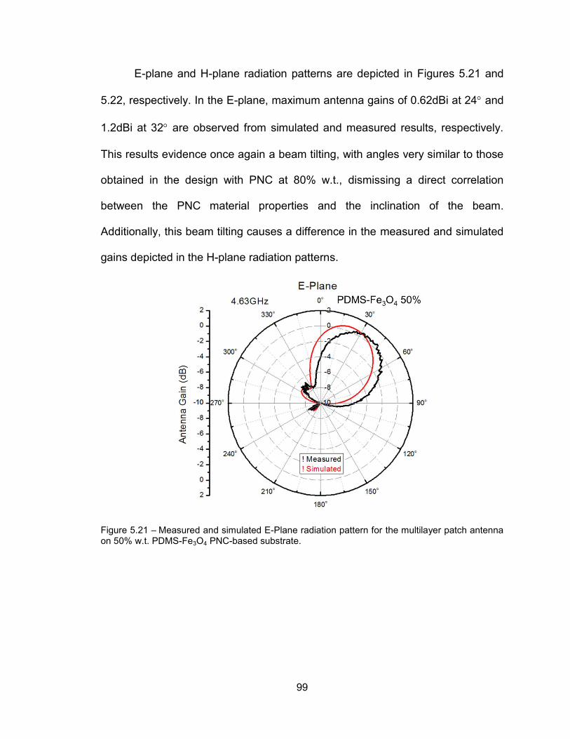
99
E-plane and H-plane radiation patterns are depicted in Figures 5.21 and
5.22, respectively. In the E-plane, maximum antenna gains of 0.62dBi at 24 and
1.2dBi at 32 are observed from simulated and measured results, respectively.
This results evidence once again a beam tilting, with angles very similar to those
obtained in the design with PNC at 80% w.t., dismissing a direct correlation
between the PNC material properties and the inclination of the beam.
Additionally, this beam tilting causes a difference in the measured and simulated
gains depicted in the H-plane radiation patterns.
Figure 5.21 – Measured and simulated E-Plane radiation pattern for the multilayer patch antenna on 50% w.t. PDMS-Fe3O4 PNC-based substrate.
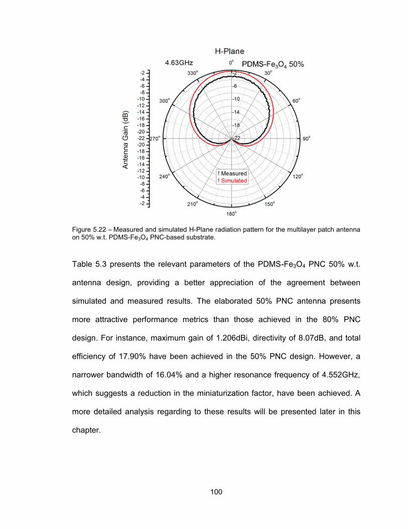
100
Figure 5.22 – Measured and simulated H-Plane radiation pattern for the multilayer patch antenna on 50% w.t. PDMS-Fe3O4 PNC-based substrate.
Table 5.3 presents the relevant parameters of the PDMS-Fe3O4 PNC 50% w.t.
antenna design, providing a better appreciation of the agreement between
simulated and measured results. The elaborated 50% PNC antenna presents
more attractive performance metrics than those achieved in the 80% PNC
design. For instance, maximum gain of 1.206dBi, directivity of 8.07dB, and total
efficiency of 17.90% have been achieved in the 50% PNC design. However, a
narrower bandwidth of 16.04% and a higher resonance frequency of 4.552GHz,
which suggests a reduction in the miniaturization factor, have been achieved. A
more detailed analysis regarding to these results will be presented later in this
chapter.
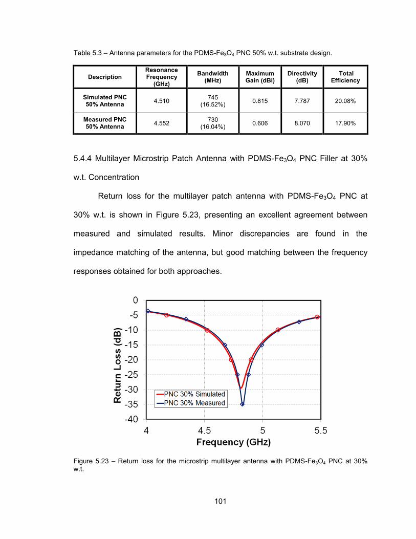
101
Table 5.3 – Antenna parameters for the PDMS-Fe3O4 PNC 50% w.t. substrate design.
Description Resonance Frequency
(GHz) Bandwidth
(MHz) Maximum Gain (dBi)
Directivity (dB)
Total Efficiency
Simulated PNC 50% Antenna 4.510 745
(16.52%) 0.815 7.787 20.08%
Measured PNC 50% Antenna 4.552 730
(16.04%) 0.606 8.070 17.90%
5.4.4 Multilayer Microstrip Patch Antenna with PDMS-Fe3O4 PNC Filler at 30%
w.t. Concentration
Return loss for the multilayer patch antenna with PDMS-Fe3O4 PNC at
30% w.t. is shown in Figure 5.23, presenting an excellent agreement between
measured and simulated results. Minor discrepancies are found in the
impedance matching of the antenna, but good matching between the frequency
responses obtained for both approaches.
Figure 5.23 – Return loss for the microstrip multilayer antenna with PDMS-Fe3O4 PNC at 30% w.t.
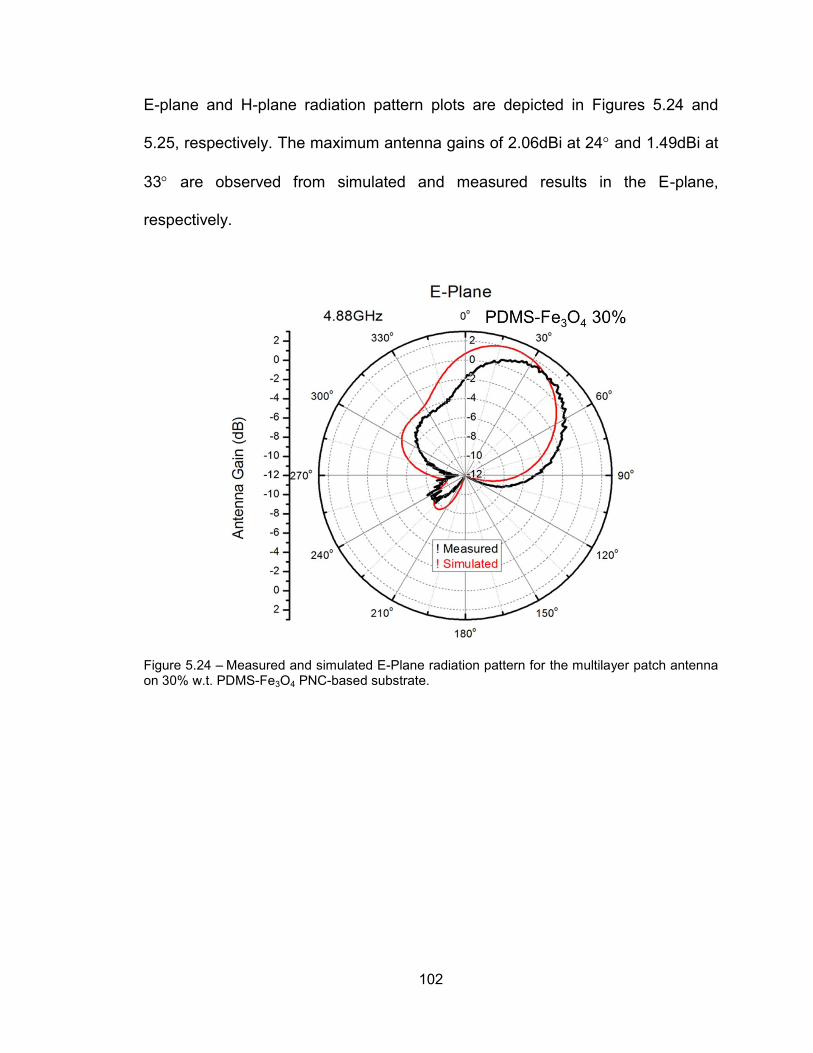
102
E-plane and H-plane radiation pattern plots are depicted in Figures 5.24 and
5.25, respectively. The maximum antenna gains of 2.06dBi at 24 and 1.49dBi at
33 are observed from simulated and measured results in the E-plane,
respectively.
Figure 5.24 – Measured and simulated E-Plane radiation pattern for the multilayer patch antenna on 30% w.t. PDMS-Fe3O4 PNC-based substrate.
103
Figure 5.25 – Measured and simulated H-Plane radiation pattern for the multilayer patch antenna on 30% w.t. PDMS-Fe3O4 PNC-based substrate.
Table 5.4 presents a comparison of measured and simulated antenna
parameters for the design with the PDMS-Fe3O4 PNC 30% w.t. substrate,
providing a better appreciation of the good agreement between simulated and
measured results. For the realized antenna, measured performance metrics are
more attractive than those achieved in the designs with PNC at 80% w.t. and
PNC at 50% w.t. For instance, maximum gain of 2.003dBi, directivity of 8.203dB,
and total efficiency of 23.98% have been obtained for this last design, surpassing
the results obtained in the other two designs that implement PNCs as substrate
fillers. However, the performance metrics of the PNC at 30% w.t. design are not
significantly better than those in the PNC 50% w.t. design, as the antenna now
exhibits a narrower bandwidth of 12.37% and a higher resonance frequency of
104
4.832GHz, which corresponds to the reduction of the miniaturization factor. More
detailed analysis regarding to these results will be provided later in this chapter.
Table 5.4 – Antenna parameters for the PDMS-Fe3O4 PNC 30% w.t. substrate design.
Description Resonance Frequency
(GHz) Bandwidth
(MHz) Maximum Gain (dBi)
Directivity (dB)
Total Efficiency
Simulated PNC 30% Antenna 4.796 595
(12.40%) 1.987 8.415 22.76%
Measured PNC 30% Antenna 4.832 597.5
(12.37%) 2.003 8.203 23.98%
5.5 Performance Comparison of Multilayer Patch Antennas Built on PDMS-Fe3O4
PNC Substrates with Different Particle Loading Concentrations
A systematic analysis of the performance of the antennas is developed,
comparing the measurement results obtained from the different designs (PDMS,
80% PNC, 50% PNC and 30% PNC). The primary antenna performance metrics,
such as return loss, antenna radiation pattern, maximum gain, directivity and
antenna efficiency are analyzed and explored for each design.
Initially, comparisons between the as-constructed antennas are presented
without the presence of any biasing magnetic field. Subsequently, comparisons
are carried out among the measurement results obtained while a DC biasing
magnetic field is applied to the antennas through the employment of a permanent
magnet in close proximity to the embedded PNC material.
5.5.1 Performance of PDMS-Fe3O4 PNC Multilayer Antennas without Externally
Applied DC Biasing Magnetic Field
Figure 5.26 compares the return losses multilayer antennas constructed
on the pure PDMS substrate and the PDMS-Fe3O4 PNC at 80% w.t. antennas
105
substrate. Both devices were designed to operate at 4GHz, resulting in
resonance frequencies of 3.931GHz and 3.981GHz for the PDMS and 80% PNC
designs, respectively. By direct comparison of the return loss responses, the
80% PNC antenna presents an attractive widened bandwidth of
26.95%(1072.5MHz), which is 5.7 times wider than the bandwidth of
4.7%(185MHz) of its plain PDMS counterpart.
Figure 5.26 – Measured return losses for plain PDMS and 80% w.t. PDMS-Fe3O4 PNC multilayer patch antennas.
As both antennas were designed for 4GHz operation, direct size
comparison between them can be performed by measuring the areas of the
patches. The miniaturization achieved by the use of PDMS-Fe3O4 PNC at 80%
w.t. concentration is evaluated by the calculation of the miniaturization
percentage and the miniaturization factor as follows:
(5.3)
106
(5.4)
where and are the physical areas of the original antenna (i.e., PDMS
antenna) and miniaturized antenna (i.e. PDMS-Fe3O4 PNC antenna),
respectively.
As mentioned in the section 5.2, the areas of the antenna patches are
594.05mm2 and 312.05mm2 for the PDMS design and the 80% PNC design,
respectively. Taking into consideration these areas, miniaturization percentage of
47.5% or miniaturization factor of 1.9 are achieved by using the PDMS-Fe3O4
PNC at 80% w.t. in the multilayer antenna configuration. Figure 5.27 clearly
shows the antenna miniaturization achieved by using embedding the PNC
underneath the antenna patch.
Figure 5.27 – Top-view photo of plain PDMS (left) and 80% w.t. PDMS-Fe3O4 PNC (right) multilayer patch antennas. A notable antenna patch size reduction of 47.5% has been achieved by the employment of 80% PNC as compared to that of the plain PDMS antenna.
However, the pure PDMS patch obtained an acceptable efficiency of 51%,
which is much better than the 12.2% efficiency obtained by the 80% PNC
antenna. Although an increased bandwidth is expected, caused by the magneto-
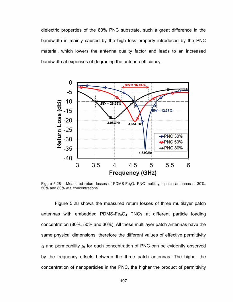
107
dielectric properties of the 80% PNC substrate, such a great difference in the
bandwidth is mainly caused by the high loss property introduced by the PNC
material, which lowers the antenna quality factor and leads to an increased
bandwidth at expenses of degrading the antenna efficiency.
Figure 5.28 – Measured return losses of PDMS-Fe3O4 PNC multilayer patch antennas at 30%, 50% and 80% w.t. concentrations.
Figure 5.28 shows the measured return losses of three multilayer patch
antennas with embedded PDMS-Fe3O4 PNCs at different particle loading
concentration (80%, 50% and 30%). All these multilayer patch antennas have the
same physical dimensions, therefore the different values of effective permittivity
r and permeability r for each concentration of PNC can be evidently observed
by the frequency offsets between the three patch antennas. The higher the
concentration of nanoparticles in the PNC, the higher the product of permittivity
108
and permeability (i.e. ) is, and then lowering the antenna resonance
frequency.
As the PNC antennas share the same physical dimensions, size
comparisons between them are conducted using their resonance frequencies. All
antenna sizes can be evaluated by finding their enlargement percentage
compared to the PNC 80% multilayer antenna :
(5.5)
where =3.981GHz is the resonance frequency of the 80% PNC multilayer
patch antenna (i.e. the reference antenna) and is the resonance frequency
of the PNC multilayer antenna with different particle loading concentration.
For the 50% PNC multilayer patch antenna =14.34%, which
means that this antenna patch is 14.34% larger than the 80% PNC counterpart.
Similarly, for the 30% PNC device, =17.61% was obtained.
To obtain a direct comparison between the plain PDMS multilayer patch
antenna and the antennas with different PNC concentrations, and then reveal the
effective miniaturization factor, the concept of equivalent area ( [ ]) is
hereby introduced. [ ] is the equivalent patch area required to build a
multilayer patch antenna at the same resonance frequency of the reference
antenna by using the PNC filler material. [ ] is found as:
[ ] (
) (5.6)
where and are the physical area and the enlargement percentage
of the referenced antenna. was calculated using Equation (5.5).
109
In order to obtain a resonance frequency of 3.981GHz (i.e. resonance
frequency of the PNC 80% multilayer patch antenna), the equivalent area for the
50% PNC is calculated using Equation (5.6):
[ ] (
)
[ ] (
)
Also, from Equation (5.6), the equivalent area at a resonance frequency of
3.981GHz is obtained for the 30% PNC antenna patch:
[ ] (
)
[ ] (
)
Now, considering the PDMS antenna as the benchmark device, the
miniaturization percentage for the 50% PNC and 30% PNC antennas can be
calculated using Equations (5.3) and (5.4), by replacing with the calculated
equivalent antenna areas:
[ ]
(5.7)
[ ] (5.8)
From Equations (5.7) and (5.8), the 50% PNC antenna patch presents
miniaturization percentage of 39.9% and miniaturization factor of 1.66. Similarly,
for the 30% PNC antenna, miniaturization percentage of 36.2% (miniaturization
factor of 1.57) was achieved.
Figure 5.29 presents the measured maximum gain in dBi for each one of
the PNC multilayer patch antennas. It is worthwhile mentioning that the antenna
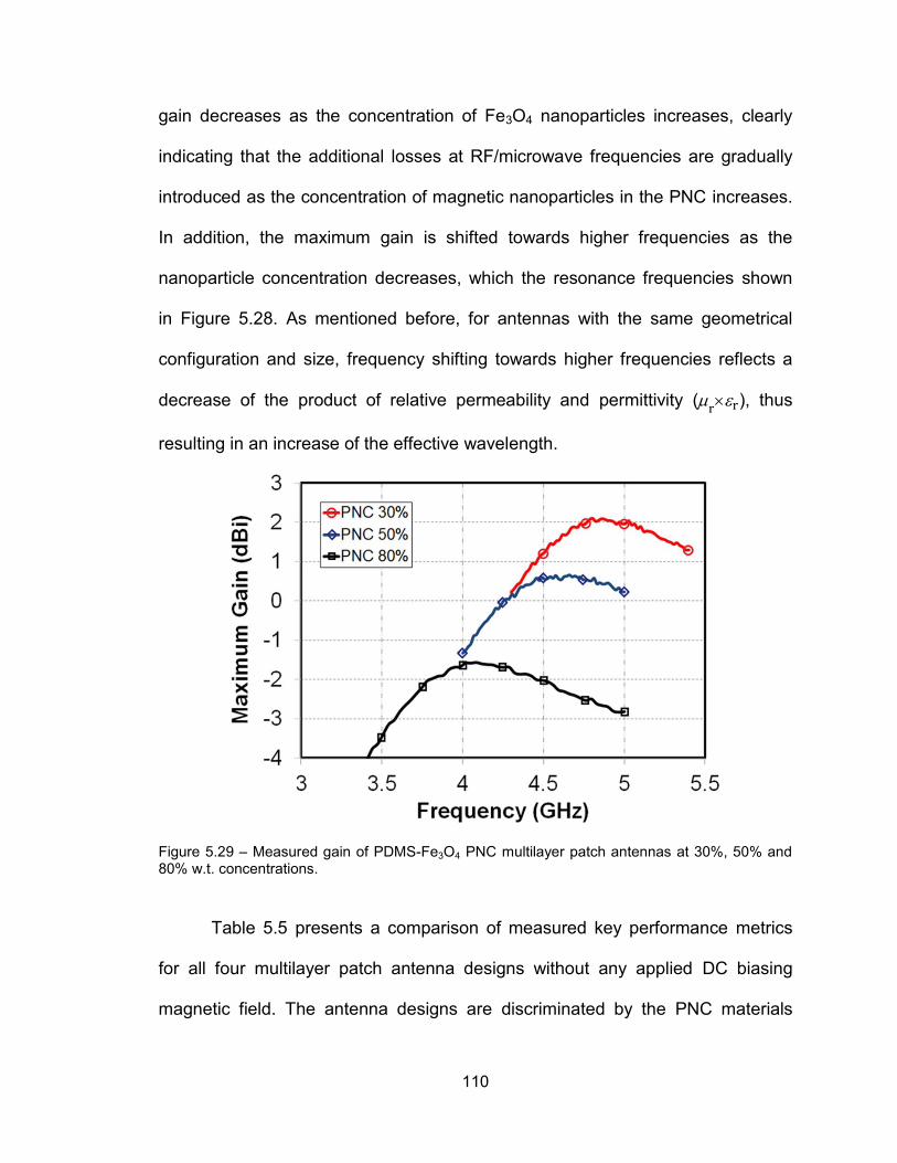
110
gain decreases as the concentration of Fe3O4 nanoparticles increases, clearly
indicating that the additional losses at RF/microwave frequencies are gradually
introduced as the concentration of magnetic nanoparticles in the PNC increases.
In addition, the maximum gain is shifted towards higher frequencies as the
nanoparticle concentration decreases, which the resonance frequencies shown
in Figure 5.28. As mentioned before, for antennas with the same geometrical
configuration and size, frequency shifting towards higher frequencies reflects a
decrease of the product of relative permeability and permittivity ( ), thus
resulting in an increase of the effective wavelength.
Figure 5.29 – Measured gain of PDMS-Fe3O4 PNC multilayer patch antennas at 30%, 50% and 80% w.t. concentrations.
Table 5.5 presents a comparison of measured key performance metrics
for all four multilayer patch antenna designs without any applied DC biasing
magnetic field. The antenna designs are discriminated by the PNC materials
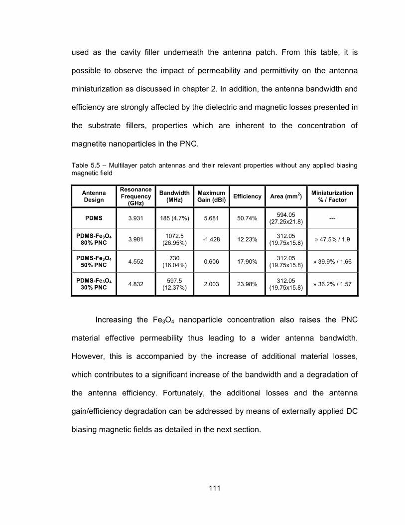
111
used as the cavity filler underneath the antenna patch. From this table, it is
possible to observe the impact of permeability and permittivity on the antenna
miniaturization as discussed in chapter 2. In addition, the antenna bandwidth and
efficiency are strongly affected by the dielectric and magnetic losses presented in
the substrate fillers, properties which are inherent to the concentration of
magnetite nanoparticles in the PNC.
Table 5.5 – Multilayer patch antennas and their relevant properties without any applied biasing magnetic field
Antenna Design
Resonance Frequency
(GHz) Bandwidth
(MHz) Maximum Gain (dBi) Efficiency Area (mm2) Miniaturization
% / Factor
PDMS 3.931 185 (4.7%) 5.681 50.74% 594.05 (27.25x21.8) ---
PDMS-Fe3O4 80% PNC 3.981 1072.5
(26.95%) -1.428 12.23% 312.05 (19.75x15.8) » 47.5% / 1.9
PDMS-Fe3O4 50% PNC 4.552 730
(16.04%) 0.606 17.90% 312.05 (19.75x15.8) » 39.9% / 1.66
PDMS-Fe3O4 30% PNC 4.832 597.5
(12.37%) 2.003 23.98% 312.05 (19.75x15.8) » 36.2% / 1.57
Increasing the Fe3O4 nanoparticle concentration also raises the PNC
material effective permeability thus leading to a wider antenna bandwidth.
However, this is accompanied by the increase of additional material losses,
which contributes to a significant increase of the bandwidth and a degradation of
the antenna efficiency. Fortunately, the additional losses and the antenna
gain/efficiency degradation can be addressed by means of externally applied DC
biasing magnetic fields as detailed in the next section.
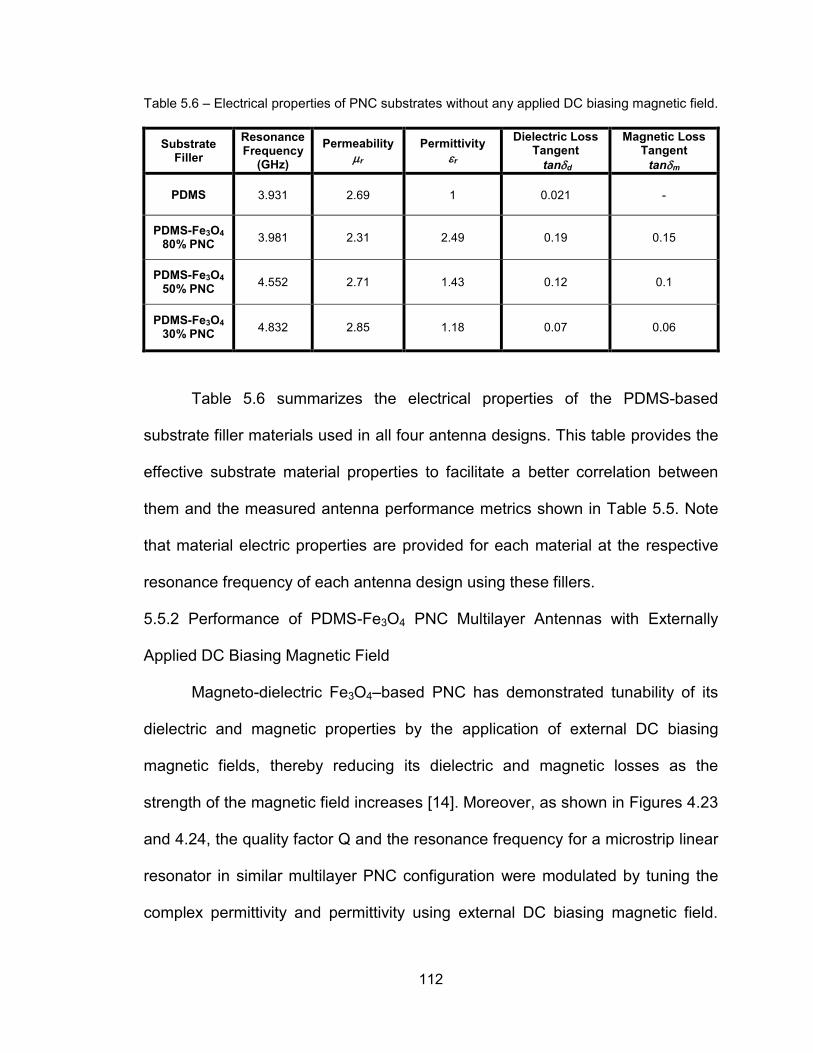
112
Table 5.6 – Electrical properties of PNC substrates without any applied DC biasing magnetic field.
Substrate Filler
Resonance Frequency
(GHz)
Permeability r
Permittivity r
Dielectric Loss Tangent
tand
Magnetic Loss Tangent
tanm
PDMS 3.931 2.69 1 0.021 -
PDMS-Fe3O4 80% PNC 3.981 2.31 2.49 0.19 0.15
PDMS-Fe3O4 50% PNC 4.552 2.71 1.43 0.12 0.1
PDMS-Fe3O4 30% PNC 4.832 2.85 1.18 0.07 0.06
Table 5.6 summarizes the electrical properties of the PDMS-based
substrate filler materials used in all four antenna designs. This table provides the
effective substrate material properties to facilitate a better correlation between
them and the measured antenna performance metrics shown in Table 5.5. Note
that material electric properties are provided for each material at the respective
resonance frequency of each antenna design using these fillers.
5.5.2 Performance of PDMS-Fe3O4 PNC Multilayer Antennas with Externally
Applied DC Biasing Magnetic Field
Magneto-dielectric Fe3O4–based PNC has demonstrated tunability of its
dielectric and magnetic properties by the application of external DC biasing
magnetic fields, thereby reducing its dielectric and magnetic losses as the
strength of the magnetic field increases [14]. Moreover, as shown in Figures 4.23
and 4.24, the quality factor Q and the resonance frequency for a microstrip linear
resonator in similar multilayer PNC configuration were modulated by tuning the
complex permittivity and permittivity using external DC biasing magnetic field.
113
The same experiment is repeated in order to demonstrate the susceptibility of the
dielectric and magnetic properties of PDMS-Fe3O4 PNC to the externally applied
DC biasing magnetic field. Basically, the employment of moderate level of DC
magnetic field result in substantial reduction of the dielectric and magnetic loss
tangents (i.e. tand and tanm), along with a noticeable increase of relative
permittivity and permeability thus enabling for more antenna miniaturization.
A stack array composed of 3 Neodymium magnets was assembled to
provide biasing DC magnetic field to the PDMS-Fe3O4 PNC embedded in the
multilayer patch antenna. The biasing magnetic field has been measured using a
DC gauss-meter (Model 1-ST from AlphaLab Inc.), at 130mils (3.3mm) of
distance from the surface, providing the approximate magnetic field strength
exerted on the embedded PNC. The gauss-meter readings showed a magnetic
field of 0.35 Tesla close to the edges and 0.20 Tesla at the center of the magnet.
These values correspond to the best operational conditions, explained in the
section 4.4. In addition, each Neodymium magnet has 2.54cm of length, 2.54cm
of width and 3mm of thickness, sufficient to cover the area in which the PNCs are
embedded in the multilayer antenna structure.
The Neodymium magnet array is placed underneath the patch and center-
aligned to PNC-filled cavity but separated by the bottom PDMS layer next to the
ground plane. Figures 5.30 (a) and (b) show how the magnet array is placed in
contact with the multilayer antenna, while Figures 5.30 (c) and (d) show how the
magnet spontaneously attaches to the antenna structure as a consequence of
the attraction with the magneto-dielectric PDMS-Fe3O4 PNC.
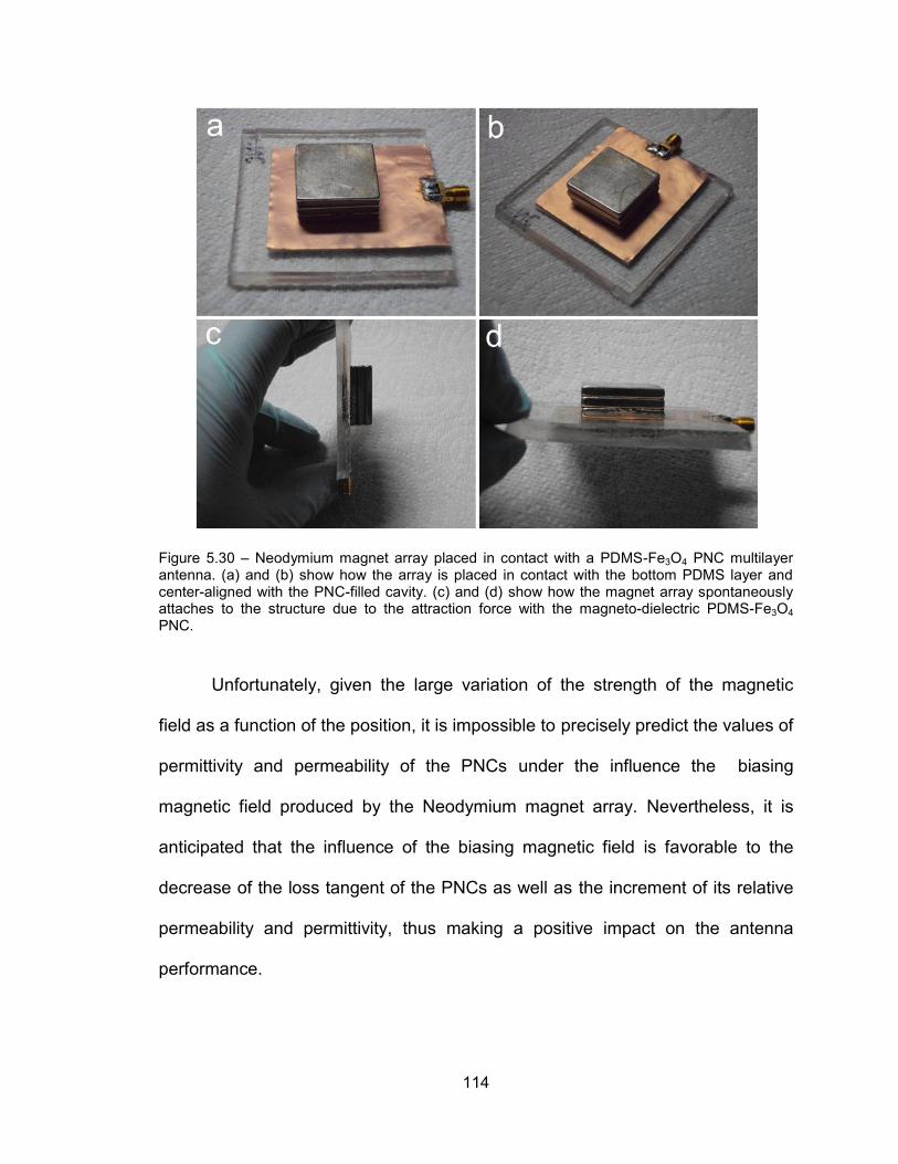
114
Figure 5.30 – Neodymium magnet array placed in contact with a PDMS-Fe3O4 PNC multilayer antenna. (a) and (b) show how the array is placed in contact with the bottom PDMS layer and center-aligned with the PNC-filled cavity. (c) and (d) show how the magnet array spontaneously attaches to the structure due to the attraction force with the magneto-dielectric PDMS-Fe3O4 PNC.
Unfortunately, given the large variation of the strength of the magnetic
field as a function of the position, it is impossible to precisely predict the values of
permittivity and permeability of the PNCs under the influence the biasing
magnetic field produced by the Neodymium magnet array. Nevertheless, it is
anticipated that the influence of the biasing magnetic field is favorable to the
decrease of the loss tangent of the PNCs as well as the increment of its relative
permeability and permittivity, thus making a positive impact on the antenna
performance.
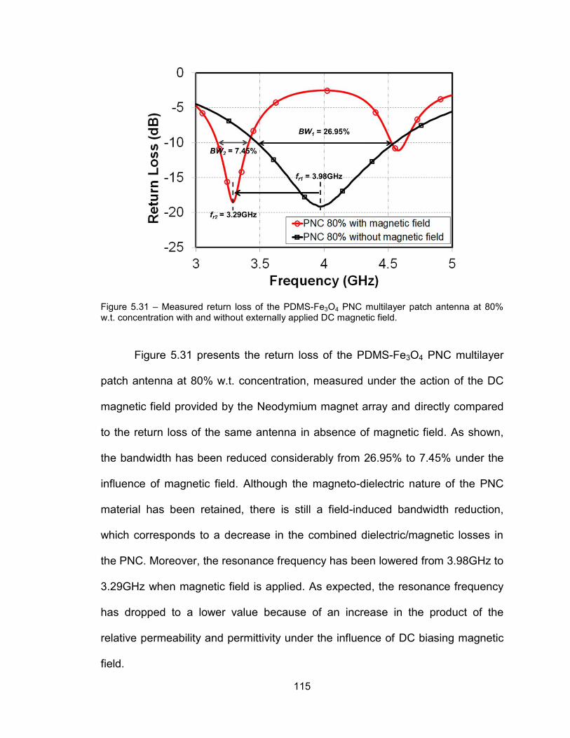
115
Figure 5.31 – Measured return loss of the PDMS-Fe3O4 PNC multilayer patch antenna at 80% w.t. concentration with and without externally applied DC magnetic field.
Figure 5.31 presents the return loss of the PDMS-Fe3O4 PNC multilayer
patch antenna at 80% w.t. concentration, measured under the action of the DC
magnetic field provided by the Neodymium magnet array and directly compared
to the return loss of the same antenna in absence of magnetic field. As shown,
the bandwidth has been reduced considerably from 26.95% to 7.45% under the
influence of magnetic field. Although the magneto-dielectric nature of the PNC
material has been retained, there is still a field-induced bandwidth reduction,
which corresponds to a decrease in the combined dielectric/magnetic losses in
the PNC. Moreover, the resonance frequency has been lowered from 3.98GHz to
3.29GHz when magnetic field is applied. As expected, the resonance frequency
has dropped to a lower value because of an increase in the product of the
relative permeability and permittivity under the influence of DC biasing magnetic
field.
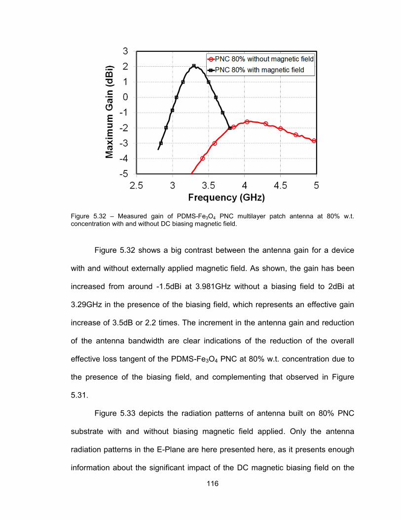
116
Figure 5.32 – Measured gain of PDMS-Fe3O4 PNC multilayer patch antenna at 80% w.t. concentration with and without DC biasing magnetic field.
Figure 5.32 shows a big contrast between the antenna gain for a device
with and without externally applied magnetic field. As shown, the gain has been
increased from around -1.5dBi at 3.981GHz without a biasing field to 2dBi at
3.29GHz in the presence of the biasing field, which represents an effective gain
increase of 3.5dB or 2.2 times. The increment in the antenna gain and reduction
of the antenna bandwidth are clear indications of the reduction of the overall
effective loss tangent of the PDMS-Fe3O4 PNC at 80% w.t. concentration due to
the presence of the biasing field, and complementing that observed in Figure
5.31.
Figure 5.33 depicts the radiation patterns of antenna built on 80% PNC
substrate with and without biasing magnetic field applied. Only the antenna
radiation patterns in the E-Plane are here presented here, as it presents enough
information about the significant impact of the DC magnetic biasing field on the
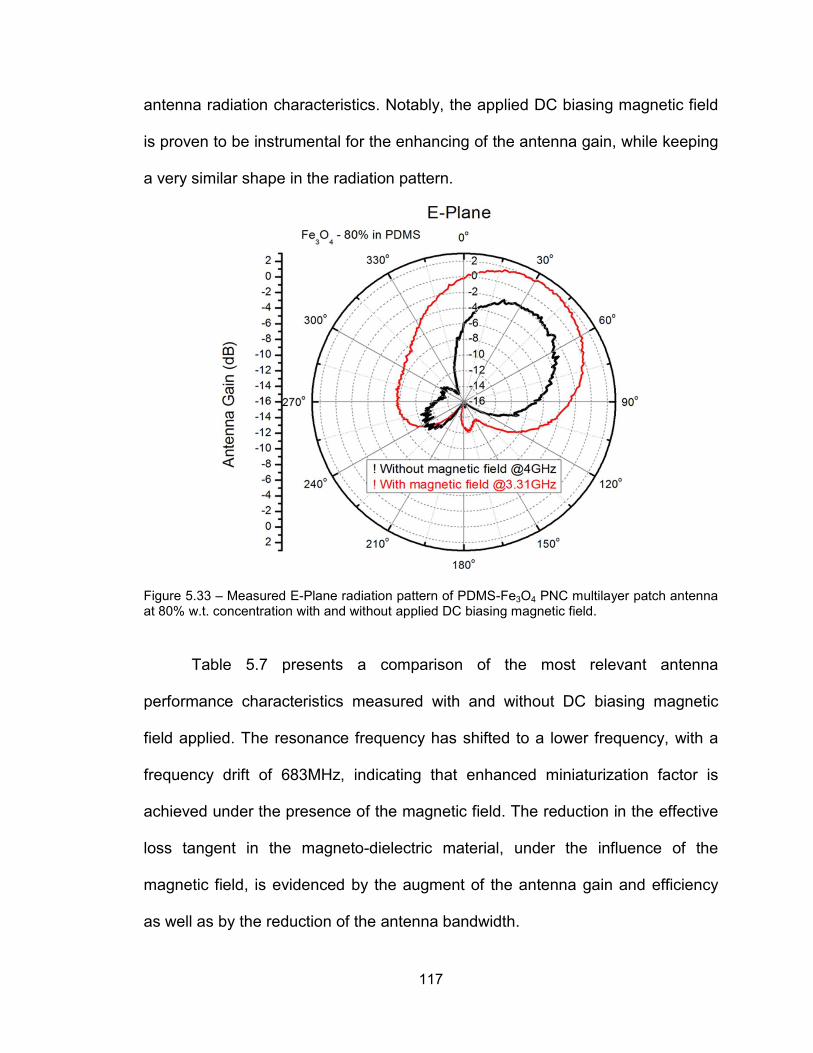
117
antenna radiation characteristics. Notably, the applied DC biasing magnetic field
is proven to be instrumental for the enhancing of the antenna gain, while keeping
a very similar shape in the radiation pattern.
Figure 5.33 – Measured E-Plane radiation pattern of PDMS-Fe3O4 PNC multilayer patch antenna at 80% w.t. concentration with and without applied DC biasing magnetic field.
Table 5.7 presents a comparison of the most relevant antenna
performance characteristics measured with and without DC biasing magnetic
field applied. The resonance frequency has shifted to a lower frequency, with a
frequency drift of 683MHz, indicating that enhanced miniaturization factor is
achieved under the presence of the magnetic field. The reduction in the effective
loss tangent in the magneto-dielectric material, under the influence of the
magnetic field, is evidenced by the augment of the antenna gain and efficiency
as well as by the reduction of the antenna bandwidth.
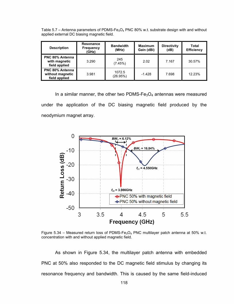
118
Table 5.7 – Antenna parameters of PDMS-Fe3O4 PNC 80% w.t. substrate design with and without applied external DC biasing magnetic field.
Description Resonance Frequency
(GHz) Bandwidth
(MHz) Maximum Gain (dBi)
Directivity (dB)
Total Efficiency
PNC 80% Antenna with magnetic field applied
3.290 245 (7.45%) 2.02 7.167 30.57%
PNC 80% Antenna without magnetic
field applied 3.981 1072.5
(26.95%) -1.428 7.698 12.23%
In a similar manner, the other two PDMS-Fe3O4 antennas were measured
under the application of the DC biasing magnetic field produced by the
neodymium magnet array.
Figure 5.34 – Measured return loss of PDMS-Fe3O4 PNC multilayer patch antenna at 50% w.t. concentration with and without applied magnetic field.
As shown in Figure 5.34, the multilayer patch antenna with embedded
PNC at 50% also responded to the DC magnetic field stimulus by changing its
resonance frequency and bandwidth. This is caused by the same field-induced
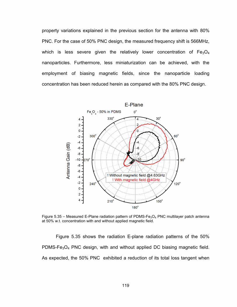
119
property variations explained in the previous section for the antenna with 80%
PNC. For the case of 50% PNC design, the measured frequency shift is 566MHz,
which is less severe given the relatively lower concentration of Fe3O4
nanoparticles. Furthermore, less miniaturization can be achieved, with the
employment of biasing magnetic fields, since the nanoparticle loading
concentration has been reduced herein as compared with the 80% PNC design.
Figure 5.35 – Measured E-Plane radiation pattern of PDMS-Fe3O4 PNC multilayer patch antenna at 50% w.t. concentration with and without applied magnetic field.
Figure 5.35 shows the radiation E-plane radiation patterns of the 50%
PDMS-Fe3O4 PNC design, with and without applied DC biasing magnetic field.
As expected, the 50% PNC exhibited a reduction of its total loss tangent when
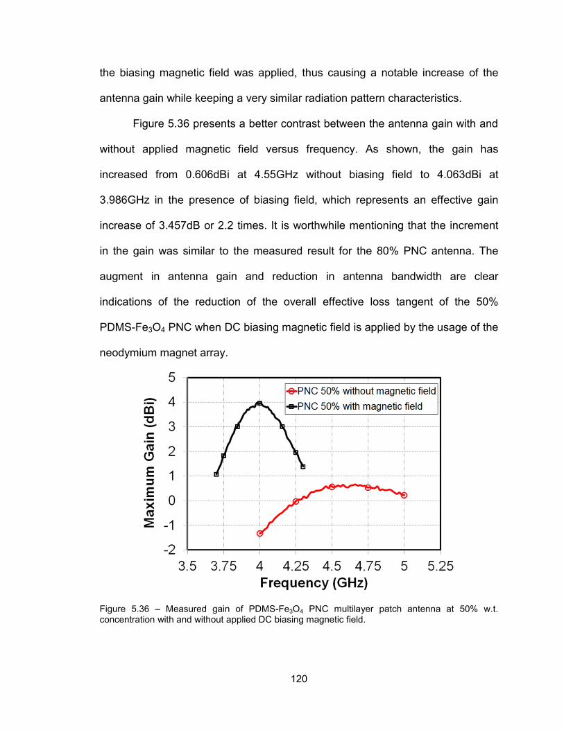
120
the biasing magnetic field was applied, thus causing a notable increase of the
antenna gain while keeping a very similar radiation pattern characteristics.
Figure 5.36 presents a better contrast between the antenna gain with and
without applied magnetic field versus frequency. As shown, the gain has
increased from 0.606dBi at 4.55GHz without biasing field to 4.063dBi at
3.986GHz in the presence of biasing field, which represents an effective gain
increase of 3.457dB or 2.2 times. It is worthwhile mentioning that the increment
in the gain was similar to the measured result for the 80% PNC antenna. The
augment in antenna gain and reduction in antenna bandwidth are clear
indications of the reduction of the overall effective loss tangent of the 50%
PDMS-Fe3O4 PNC when DC biasing magnetic field is applied by the usage of the
neodymium magnet array.
Figure 5.36 – Measured gain of PDMS-Fe3O4 PNC multilayer patch antenna at 50% w.t. concentration with and without applied DC biasing magnetic field.
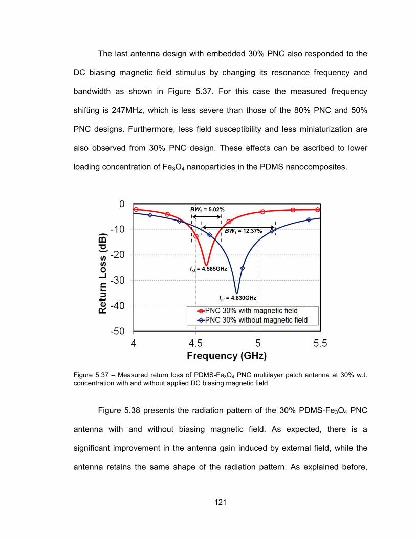
121
The last antenna design with embedded 30% PNC also responded to the
DC biasing magnetic field stimulus by changing its resonance frequency and
bandwidth as shown in Figure 5.37. For this case the measured frequency
shifting is 247MHz, which is less severe than those of the 80% PNC and 50%
PNC designs. Furthermore, less field susceptibility and less miniaturization are
also observed from 30% PNC design. These effects can be ascribed to lower
loading concentration of Fe3O4 nanoparticles in the PDMS nanocomposites.
Figure 5.37 – Measured return loss of PDMS-Fe3O4 PNC multilayer patch antenna at 30% w.t. concentration with and without applied DC biasing magnetic field.
Figure 5.38 presents the radiation pattern of the 30% PDMS-Fe3O4 PNC
antenna with and without biasing magnetic field. As expected, there is a
significant improvement in the antenna gain induced by external field, while the
antenna retains the same shape of the radiation pattern. As explained before,
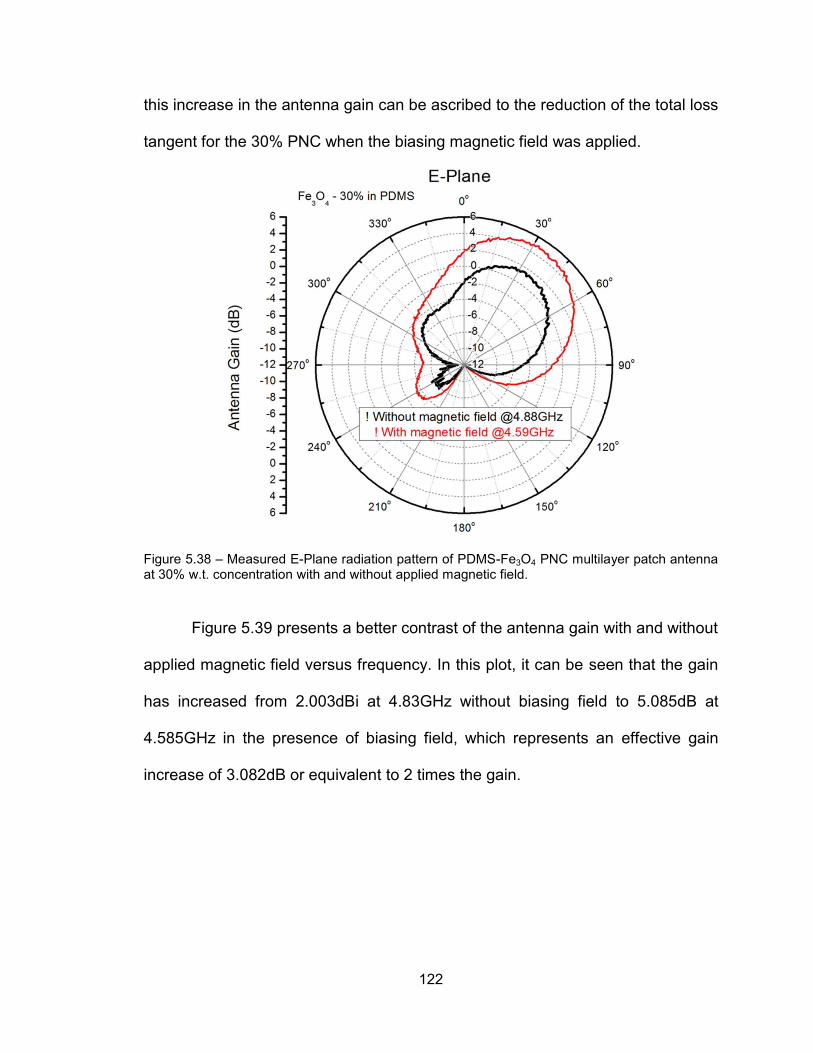
122
this increase in the antenna gain can be ascribed to the reduction of the total loss
tangent for the 30% PNC when the biasing magnetic field was applied.
Figure 5.38 – Measured E-Plane radiation pattern of PDMS-Fe3O4 PNC multilayer patch antenna at 30% w.t. concentration with and without applied magnetic field.
Figure 5.39 presents a better contrast of the antenna gain with and without
applied magnetic field versus frequency. In this plot, it can be seen that the gain
has increased from 2.003dBi at 4.83GHz without biasing field to 5.085dB at
4.585GHz in the presence of biasing field, which represents an effective gain
increase of 3.082dB or equivalent to 2 times the gain.
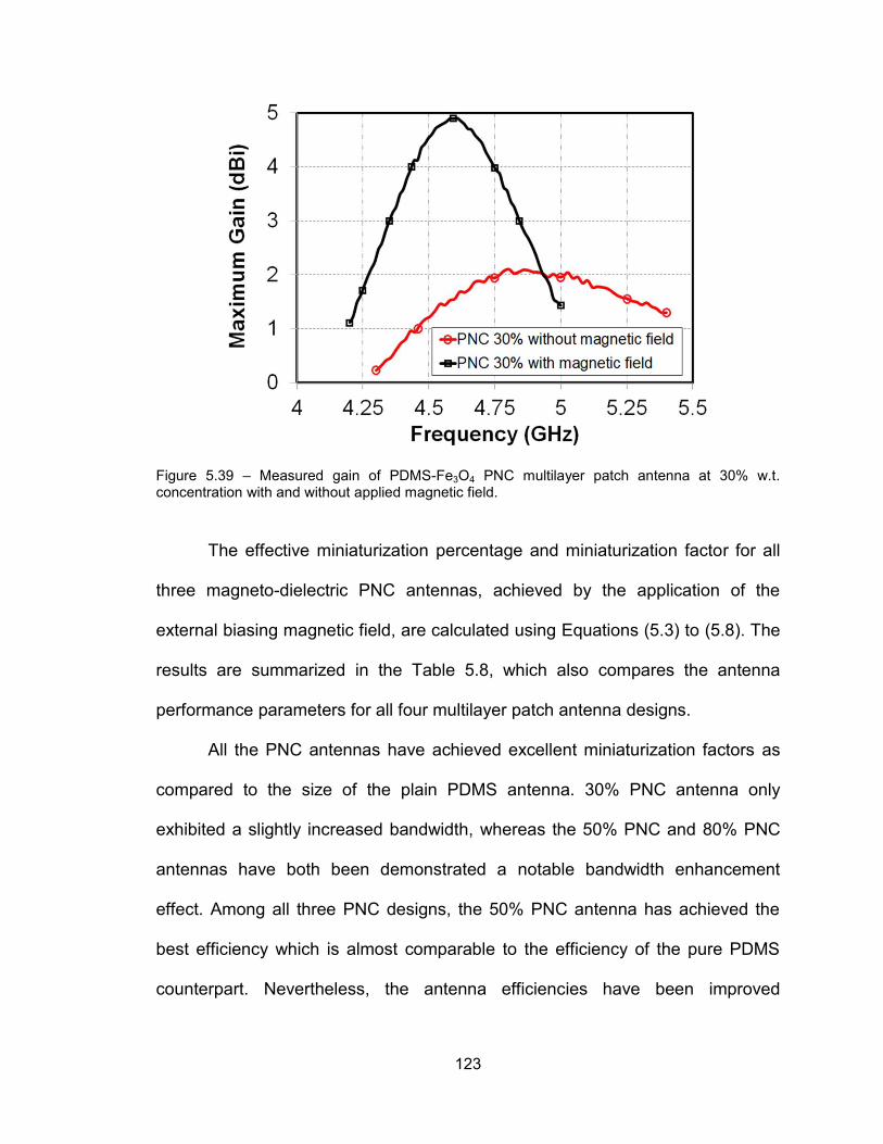
123
Figure 5.39 – Measured gain of PDMS-Fe3O4 PNC multilayer patch antenna at 30% w.t. concentration with and without applied magnetic field.
The effective miniaturization percentage and miniaturization factor for all
three magneto-dielectric PNC antennas, achieved by the application of the
external biasing magnetic field, are calculated using Equations (5.3) to (5.8). The
results are summarized in the Table 5.8, which also compares the antenna
performance parameters for all four multilayer patch antenna designs.
All the PNC antennas have achieved excellent miniaturization factors as
compared to the size of the plain PDMS antenna. 30% PNC antenna only
exhibited a slightly increased bandwidth, whereas the 50% PNC and 80% PNC
antennas have both been demonstrated a notable bandwidth enhancement
effect. Among all three PNC designs, the 50% PNC antenna has achieved the
best efficiency which is almost comparable to the efficiency of the pure PDMS
counterpart. Nevertheless, the antenna efficiencies have been improved
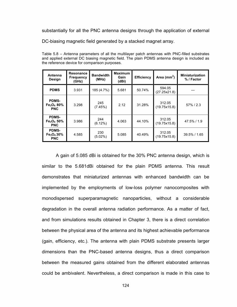
124
substantially for all the PNC antenna designs through the application of external
DC-biasing magnetic field generated by a stacked magnet array.
Table 5.8 – Antenna parameters of all the multilayer patch antennas with PNC-filled substrates and applied external DC biasing magnetic field. The plain PDMS antenna design is included as the reference device for comparison purposes.
Antenna Design
Resonance Frequency
(GHz) Bandwidth
(MHz) Maximum
Gain (dBi)
Efficiency Area (mm2) Miniaturization % / Factor
PDMS 3.931 185 (4.7%) 5.681 50.74% 594.05 (27.25x21.8) ---
PDMS-Fe3O4 80%
PNC 3.298 245
(7.45%) 2.12 31.28% 312.05 (19.75x15.8) 57% / 2.3
PDMS-Fe3O4 50%
PNC 3.986 244
(6.12%) 4.063 44.10% 312.05 (19.75x15.8) 47.5% / 1.9
PDMS-Fe3O4 30%
PNC 4.585 230
(5.02%) 5.085 40.49% 312.05 (19.75x15.8) 39.5% / 1.65
A gain of 5.085 dBi is obtained for the 30% PNC antenna design, which is
similar to the 5.681dBi obtained for the plain PDMS antenna. This result
demonstrates that miniaturized antennas with enhanced bandwidth can be
implemented by the employments of low-loss polymer nanocomposites with
monodispersed superparamagnetic nanoparticles, without a considerable
degradation in the overall antenna radiation performance. As a matter of fact,
and from simulations results obtained in Chapter 3, there is a direct correlation
between the physical area of the antenna and its highest achievable performance
(gain, efficiency, etc.). The antenna with plain PDMS substrate presents larger
dimensions than the PNC-based antenna designs, thus a direct comparison
between the measured gains obtained from the different elaborated antennas
could be ambivalent. Nevertheless, a direct comparison is made in this case to
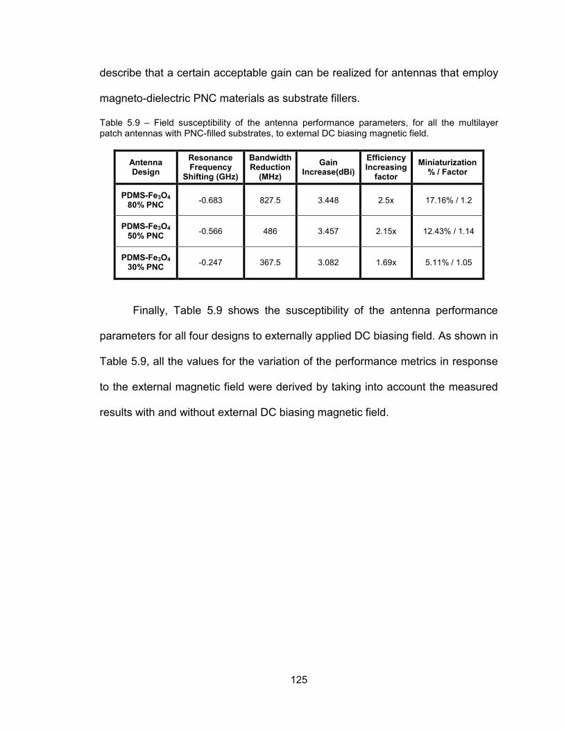
125
describe that a certain acceptable gain can be realized for antennas that employ
magneto-dielectric PNC materials as substrate fillers.
Table 5.9 – Field susceptibility of the antenna performance parameters, for all the multilayer patch antennas with PNC-filled substrates, to external DC biasing magnetic field.
Antenna Design
Resonance Frequency
Shifting (GHz)
Bandwidth Reduction
(MHz) Gain
Increase(dBi) Efficiency Increasing
factor Miniaturization
% / Factor
PDMS-Fe3O4 80% PNC -0.683 827.5 3.448 2.5x 17.16% / 1.2
PDMS-Fe3O4 50% PNC -0.566 486 3.457 2.15x 12.43% / 1.14
PDMS-Fe3O4 30% PNC -0.247 367.5 3.082 1.69x 5.11% / 1.05
Finally, Table 5.9 shows the susceptibility of the antenna performance
parameters for all four designs to externally applied DC biasing field. As shown in
Table 5.9, all the values for the variation of the performance metrics in response
to the external magnetic field were derived by taking into account the measured
results with and without external DC biasing magnetic field.
126
Chapter 6
Conclusions and Future Work
6.1 Summary and Contributions to the RF/Microwave Field
This research has presented the usage of magnetite-based magneto-
dielectric polymer nanocomposites for the implementation of miniaturized
multilayer patch antennas. Four different patch antenna designs were
systematically explored. Each one of the PDMS-based design has a different
loading concentration of superparamagnetic nanoparticles (from 0% to 80%).
The performance of the constructed antennas was measured with and without
externally applied DC biasing magnetic field. Comparisons between the different
designs were thoroughly conducted to demonstrate the correlation between the
nanoparticle loading concentration presented in the polymer nanocomposites
and the corresponding resultant dielectric and magnetic properties.
Antenna miniaturization up to 57% and antenna bandwidth increase of
58% (from 4.7% to 7.45%) have been successfully demonstrated, while retaining
an acceptable antenna gain by the employment of PDMS-Fe3O4 PNC with 80%
w.t. concentration. Furthermore, the reduction of the loading concentration of the
superparamagnetic nanoparticles in the PNC (e.g. 50% w.t. PNC and 30%w.t.
PNC) decreased the dielectric and magnetic loss properties, then resulting in the
enhancement of the antenna gain, up to the value close to that achieved by its
pure PDMS counterpart. Beyond acknowledging that the reduction of
127
nanoparticle loading does decrease the permeability of the resultant PNC,
thereby reducing both bandwidth miniaturization factor of the multilayer antenna,
it is paramount to notice that resulting magneto-dielectric characteristics of the
PDMS-Fe3O4 nanocomposite materials with low nanoparticle concentrations, do
offer superior electrical properties when compared to pure PDMS substrates. For
instance, the antenna with embedded PDMS-Fe3O4 PNC at 30% w.t. has
exhibited a gain of 5.085dBi, similar to the measured gain of 5.095dBi of the pure
PDMS antenna. Additionally, the antenna with the PNC at 30% w.t. presented
slightly increased bandwidth of 5.02% (as compared to the 4.7% for pure PDMS
counterpart), together with a significant miniaturization of 39.5%, which enables
1.65 times smaller antenna dimensions.
In conclusion, the novelty of this dissertation work is the fact that it
represents the first known successful attempt when PDMS-Fe3O4 magneto-
dielectric polymer nanocomposites have been effectively employed for the
miniaturization and bandwidth enhancement of microstrip patch antennas.
Finally, the demonstration of tunability of the antenna characteristics (i.e.,
resonance frequency and radiation properties), under externally applied DC
magnetic fields generated by permanent magnets, opens alternate approaches
for further research and implementation of reconfigurable antennas as well as
tunable antenna arrays.
6.2 Recommendation for Future Work and Emerging Projects
The methodologies and experiments developed in this dissertation work
can be used as the baseline for the implementation of multilayer planar antennas
128
that employ low-loss superparamagnetic polymer nanocomposites systems as
substrates. Certainly, there is room for further improvement beyond the results
reported herein. Initially, efforts should focus on how to mitigate dielectric and
magnetic losses of magneto-dielectric nanocomposites, especially while they
present high particle loading concentrations. New magneto-dielectric polymer
nanocomposites can be developed by selecting different polymer matrices and
nanoparticles. The selection of a polymer with very low dielectric losses will help
improve antenna performance. Factors such as the compatibility with the
nanoparticle system and the solvents used for the nanoparticle suspension
should be considered. In future work, the use of inorganic coating for the purpose
of surface functionalization should be explored. Aside from reducing the loss
associated with organic surfactant, the usage of inorganic coating can further
improve the compatibility with existing polymers that require high curing
temperatures (e.g., PTFE based polymers).
Furthermore, magneto-dielectric polymer nanocomposites may be used in
other antenna topologies in order to achieve increased miniaturization and
maximize the antenna performance (i.e., antenna gain, bandwidth), while taking
full advantage of the properties of these new polymeric materials.
Similarly, other topologies can potentially take advantage of magneto-
dielectric materials with controllable values of and . With the magneto-
dielectric PNCs developed in this dissertation work, antennas based on artificial
magneto-dielectric material, such as the design proposed by Namin et al. at [1],
may now become realizable.

129
Finally, the magneto-dielectric PNC materials developed in this work can
be investigated simultaneously with Electromagnetic Band Gap Structures and
Frequency Selective Surfaces. The proper implementation of magneto-dielectric
PNC in such structures may help improve their operational frequency range and
provide additional miniaturization.
130
References
[1] F. Namin, T. G. Spence, D. H. Werner and E. Semouchkina, “Broadband, Miniaturized Stacked-Patch Antennas for L-Band Operation Based on Magneto-Dielectric Substrates,” IEEE Transactions on Antennas and Propagation, vol. 58, no. 9, pp. 2817-2822, September 2010.
[2] J. L. Volakis, C. C. Chen and K. Fujimoto, “Small Antennas [Electronic Resource]: Miniaturization Techniques & Applications,” McGraw-Hill, New York, 2010
[3] F. Erkmen, Chi-Chih Chen and J. L. Volakis, “Impedance Matched Ferrite Layers as Ground Plane Treatments to Improve Antenna Wide-Band Performance,” IEEE Transactions on Antennas and Propagation, vol. 57, no. 1, pp. 263-266, 2009.
[4] K. N. Rozanov, I. T. Iakubov, A. N. Lagarkov, S. A. Maklakov, A. V. Osipov, D. A. Petrov, L. Ryzhikov, M. V. Sedova and S. N. Starostenko, “Laminates of thin ferromagnetic films for microwave applications,” The Sixth International Kharkov Symposium on Physics and Engineering of Microwaves, Millimeter and Submillimeter Waves and Workshop on Terahertz Technologies, 2007. MSMW '07., 2007, pp. 168-173.
[5] C.A Balanis, “Advanced Engineering Electromagnetics,” John Wiley and Sons, Inc. 1989, pp. 181-243.
[6] R.C. Hansen and M. Burke, “Antennas with magneto-dielectrics,” Microwave Optical Technology Letters, vol. 26, no. 2, pp.75-78, July 2000.
[7] H. A. Wheeler, “Transmission-Line Properties of Parallel Strips Separated by a Dielectric Sheet,” IEEE Transactions on Microwave Theory and Techniques, vol. 13, no. 2, pp. 172-185, 1965.
131
[8] S. Sun and H. Zeng, “Size-Controlled Synthesis of Magnetite Nanoparticles,” Journal of the American Chemical Society., vol. 124, no. 28, pp. 8204-8205, July 2002.
[9] R.M. Cornell, U. Schwertmann, “The Iron Oxides: Structure, Properties, Reactions, Occurrence and Uses,” VCH, New York, 1996, pp28-29.
[10] L. Fu, V. P. Dravid and D. L. Johnson, “Self-assembled (SA) bilayer molecular coating on magnetic nanoparticles,” Applied Surface Science, vol. 181, no.1-2, pp. 173-178, 9/3, 2001.
[11] N. A. Frey, S. Peng, K. Cheng and S. Sun, “Magnetic nanoparticles: synthesis, functionalization, and applications in bioimaging and magnetic energy storage,” Chemical Society Reviews, vol. 38, no. 9, pp. 2532-2542, 2009.
[12] Z. Xu, C. Shen, Y. Hou, H. Gao and S. Sun, “Oleylamine as Both Reducing Agent and Stabilizer in a Facile Synthesis of Magnetite Nanoparticles,” Chemistry of Materials, vol. 21, no. 9, pp. 1778-1780, 2009.
[13] J. L. Wilson, P. Poddar, N. A. Frey, H. Srikanth, K. Mohomed, J. P. Harmon, S. Kotha and J. Wachsmuth, “Synthesis and magnetic properties of polymer nanocomposites with embedded iron nanoparticles,” Journal of Applied Physics, vol. 95, pp. 1439-1443, 2004.
[14] C. Morales, J. Dewdney, S. Pal, S. Skidmore, K. Stojak, H. Srikanth, T. Weller and Jing Wang, “Tunable Magneto-Dielectric Polymer Nanocomposites for Microwave Applications,” IEEE Transactions on Microwave Theory and Techniques, vol. MTT-59, pp. 302-310, 2011.
[15] S. Pal, S. Chandra, M.H. Phan, P. Mukherjee and H. Srikanth, “Carbon nanostraws: nanotubes filled with superparamagnetic nanoparticles,” Nanotechnology, vol. 20, no. 48, pp. 485604 (7), 2009.
[16] K Stojak, S Pal, H Srikanth, C Morales, J Dewdney, T Weller and J Wang “Polymer nanocomposites exhibiting magnetically tunable microwave properties,” Nanotechnology, vol. 22, no. 13, pp. 135602 (6), 2011.
132
[17] S. Sun, H. Zeng, D. B. Robinson, S. Raoux, P. M. Rice, S. X. Wang and G. Li, “Monodisperse MFe2O4 (M = Fe, Co, Mn) Nanoparticles,” Journal of the American Chemical Society, vol. 126, no. 1, pp. 273-279, 2004.
[18] J. Gass, P. Poddar, J. Almand, S. Srinath and H. Srikanth, “Superparamagnetic Polymer Nanocomposites with Uniform Fe3O4 Nanoparticle Dispersions,” Advanced Functional Materials, vol. 16, no. 1, pp. 71-75, 2006.
[19] J.D. Hanawalt, H.W. Rinn and L.K Frevel, “Chemical Analysis by X-Ray Diffraction,” Analytical Chemistry, vol. 10, no.9, pp. 457-512, 1938.
[20] Dow Corning, Sylgard 184 Elastomer Kit Product Information, http://www.dowcorning.com/applications/search/products/Details.aspx?prod=01064291&type=PROD
[21] B. Bakar and L.F. Lemmens, “Blocking temperature in magnetic nanoclusters,” Physical Review E, vol. 71, pp. 046109 (1-7), 2005
[22] W. B. Weir, “Automatic measurement of complex dielectric constant and permeability at microwave frequencies,” Proceedings of the IEEE, vol. 62, no.1, pp. 33–36, Jan. 1974.
[23] A. M. Nicolson and G. F. Ross, “Measurement of the intrinsic properties of materials by time-domain techniques,” IEEE Transactions on Instrumentation and Measurement, vol. IM-19, no. 11, pp. 377–382, Nov. 1970.
[24] E. Hammerstad and O. Jensen, “Accurate models for microstrip computer-aided design,” in IEEE MTT-S International Microwave Symposium Digest, May 1980, pp. 407–409.
[25] M. Kirschning and R. H. Jansen, “Accurate model for effective dielectric constant of microstrip with validity up to millimetre-wave frequencies,” Electronics Letters., vol. 18, no. 6, pp. 272–273, Mar. 1982.
133
[26] J. Barker-Jarvis, E. Vanzura, and W. Kissick, “Improved technique for determining complex permittivity with the transmission/reflection method,” IEEE Transactions on Microwave Theory and Techniques, vol. 38, no. 8, pp. 1096–1103, Aug. 1990.
[27] E. Yamashita, “Variational method for the analysis of microstrip-like transmission lines,” IEEE Transactions on Microwave Theory and Techniques, vol. MTT-16, no. 8, pp. 529–535, Aug. 1968.
[28] A. Farrar and A. T. Adams, “Multilayer microstrip transmission lines,” IEEE Transactions on Microwave Theory and Techniques, vol. MTT-22, no. 10, pp. 889–891, Oct. 1974.
[29] R. A. Pucel and D. J. Masse, “Microstrip propagation on magnetic substrates—Part I: Design theory,” IEEE Transactions on Microwave Theory and Techniques, vol. MTT-20, no. 5, pp. 304–308, May 1972.
[30] H. A. Wheeler, “Transmission line properties of parallel wide strips by a conformal mapping approximation,” IEEE Transactions on Microwave Theory and Techniques, vol. MTT-12, no. 3, pp. 280–289, May 1964.
[31] J. Svacina, “Analysis of multilayer microstrip lines by a conformal mapping method,” IEEE Transactions on Microwave Theory and Techniques, vol. MTT-40, no. 4, pp. 769–772, Apr. 1992.
[32] J. Svacina, “A simple quasi-static determination of basic parameters of multilayer microstrip and coplanar waveguide,” IEEE Microwave and Guided Wave Letters, vol. 2, no. 10, pp. 385–387, Oct. 1992.
[33] T. Kaneki, “Analysis of linear microstrip using an arbitrary ferromagnetic substance as the substrate,” Electronics Letters, vol. 5, no. 19, pp. 463–465, Sep. 1969.
[34] W. Eisenstadt and Y. Eo, “S-parameter-based IC interconnect transmission line characterization,” IEEE Transactions on Components, Hybrids, and Manufacturing Technology, vol. 15, no. 4, pp. 483–490, Aug. 1992.
134
[35] C. Morales, J. Dewdney, S. Pal, K. Stojak, H. Srikanth, J. Wang, and T. Weller, “Magnetically tunable nanocomposites for microwave applications,” IEEE MTT-S International Microwave Symposium Digest, May 2010, pp. 1340–1343.
[36] J. L. Volakis, “Antenna Engineering Handbook,” 4th ed., McGraw-Hill, New York, 2007.
[37] Rogers Corporation, “ULTRALAM® 3000 Liquid Crystalline Polymer Circuit Material,” datasheet RF1.3000, publication #92-125. http://www.rogerscorp.com/documents/730/acm/ULTRALAM-3000-LCP laminate-data-sheet-ULTRALAM-3850.aspx.
About the Author
Cesar Morales received his B.S. degree (Honors) from Universidad del
Norte (University of North), Barranquilla, Colombia, in 2004; his M.S. degree in
electrical engineering from the University of South Florida, Tampa, in 2008, and
is currently working towards his Ph.D. degree in electrical engineering at the
University of South Florida. He is currently with the RF-MEMS Transducers
Group (a division of the WAMI Center), Electrical Engineering Department,
University of South Florida. His areas of research are general RF and
Microwaves, RF and microwave measurements and antenna design. He also
worked as an Engineering Intern at Modelithics Inc., in Tampa FL from 2007 to
2008. Mr. Morales is a Student Member of the Institute of Electrical and
Electronics Engineers (IEEE) and the IEEE Microwave Theory and Techniques
(MTT) Society, where he has served as reviewer for at least four Journal
Publications. He is also a member if the International Microelectronics and
Packaging Society (IMAPS) since 2008. His current research involves the
characterization and implementation of polymer nanocomposites for microwave
applications.