ldp-qcw 300-12 manual rev1602 - startseite -...
TRANSCRIPT

User Manual Rev. 16.02
LDP-QCW 300-12
PicoLAS GmbH `çãé~åó=Ñçê=fååçî~íáîÉ=mçïÉê=bäÉÅíêçåáÅë==~åÇ=i~ëÉê=qÉÅÜåçäçÖó==h~áëÉêëíê~ëëÉ=NMM=abJ=RONPQ=eÉêòçÖÉåê~íÜ==mÜçåÉW== HQV=EMF=OQMTJRSP=RUJM=c~ñW= = HQV=EMF=OQMTJRSP=RUJOV=bJj~áäW== áåÑç]éáÅçä~ëKÇÉ=tÉÄW= = ïïïKéáÅçä~ëKÇÉ=

2
Table of Contents LDP-QCW 300-12 ...................................................................................................................................1 Table of Contents .....................................................................................................................................2 How to use the Manual.............................................................................................................................3 How to get started (refer to drawings on next 2 pages) ............................................................................4 Description of available Connectors.........................................................................................................5 Interface Specifications ............................................................................................................................6 Dos and Don’ts.......................................................................................................................................10 Functional Description ...........................................................................................................................11 Trigger modes.........................................................................................................................................12 Regulator ................................................................................................................................................15 LED codes ..............................................................................................................................................17 Power Supply .........................................................................................................................................17 Cooling...................................................................................................................................................17 Test Load................................................................................................................................................17 Over Temperature Shutdown .................................................................................................................18 Absolute Maximum Ratings...................................................................................................................18 Mechanical Dimensions .........................................................................................................................19 Controlling the LDP-QCW using a PLB-21...........................................................................................20 Controlling the LDP-QCW via RS232...................................................................................................23 The PicoLAS Protocol............................................................................................................................31
3
How to use the Manual
Remark: The LDP-QCW described in this manual is a base-plate cooled laser diode driver. Improper cooling may cause an internal over temperature shutdown. The two fans in one side of the unit have to prevent local thermal hot spots inside the unit. They can not compensate improper base plate cooling. The air inside an enclosure within an OEM application is usually enough to yield enough air flow. Please do not cover any ventilation slots.
Base plate cooling: Depending on the final application and operation regime, this unit may stay none-cooled or must be assembled onto a heat sink.
Please refer to chapter Power dissipation for more details about the thermal power losses during operation.
You me use a passively or an actively air/water cooled device.
Housing: All units are delivered with housing. Changes are possible; the units can be delivered without housing upon request.
Before powering on your unit, read this manual thoroughly and make sure your understood it fully.
Please pay attention to all safety warnings.
If you have any doubt or suggestion, please do not hesitate to contact us!

4
How to get started (refer to drawings on next 2 pages)
Step # What to do Check
1 Unpack your device and place it in front of you as shown on the next page.
2 Connect a load (for example your laser diode) to the output.
Make sure to use both anode and cathode connectors in parallel.
3 Connect the PLB-21 or an RS232 cable A driver is required in order to use the LDP-QCW with a PC. See chapter “Controlling the LDP-QCW via PC” for more information
4 Connect the input power supply; make sure that polarity is correct. The supply voltage must be at least 24 V and about 5 V above the desired capacitor bank voltage.
Make sure that your power supply does not have any voltage overshoots when
switching on or off. Do not exceed the maximum operating voltage of 48 V
5 Switch the power supply on
6 If a PLB-21 is used, its display may show a message about downloading a new driver. Confirm this with YES.
See chapter “Controlling the LDP-QCW using a PLB-21” for more information
7 Set all required parameters using the PLB-21 or RS232 interface
See chapter “Controlling the LDP-QCW using a PLB-21” for more information
8 Apply +5V to the MasterEnable pin of the BOB connector
See chapter “Interface specifications” for more information
9 Apply +5V to the Enable pin of the BOB connector. This will enable the output
See chapter “Interface specifications” for more information
10 Monitor the current pulses using an oscilloscope connected to the current monitor output
See chapter “Interface specifications” for more information
11 Verify that the PULSER_OK signal is +5V See chapter “Interface specifications” for more information

5
Description of available Connectors The following drawing shows all connections which are available to the user.
LDP-C BOB
Connector
See section interface specifications for detailed information. (Break-out-board connector.)
PLB Connector for PLB-21 (protected against polarity reversal)
Vin Supply voltage
GND Supply ground
LD+ Positive laser diode output (anode). Use both connectors parallel for high currents.
LD- Negative laser diode output (cathode). Do not connect to ground! Use both connectors parallel for high currents.
For a more convenient use of the driver (e.g. in laboratory use) we recommend the optional available product accessory LDP-C-BOB. Please see LDP-C-BOB manual for further details.

6
`çååÉÅíáåÖ=~åÇ=fåíÉêÑ~ÅáåÖ==
=qÜÉ=Ä~ëÉéä~íÉ=áë=áåíÉêå~ääó=åçí=ÅçååÉÅíÉÇ=íç=dka=íç=~îçáÇ=dkaJäççé=ÅìêêÉåíëK=qÜÉ=ÅÜ~ëëáë=L=Ä~ëÉéä~íÉ=ãìëí=ÄÉ=ÖêçìåÇÉÇ=Äó=íÜÉ=ìëÉê>==
=
qÜÉ=ã~ñáãìã=îçäí~ÖÉ=ÄÉíïÉÉå=dka=~åÇ=`Ü~ëëáë=áë=QU=sK=bñÅÉÉÇáåÖ=íÜáë=îçäí~ÖÉ=ïáää=Ç~ã~ÖÉ=íÜÉ=ÇêáîÉê=~åÇ=L=çê=ïáää=Å~ìëÉ=ÅçããìåáÅ~íáçå=ÉêêçêëK==
qÜáë=áë=åçí=ÅçîÉêÉÇ=Äó=ï~êê~åíó=>=
píêáÅíäó=~îçáÇ=ÖêçìåÇ=äççé=ÅìêêÉåíë=íÜêçìÖÜ=íÜÉ=ÅçåíêçääáåÖ=áåíÉêÑ~ÅÉ>==
=
cêçåí=îáÉï=
=
pÉêá~ä=ëíáÅâÉê=
fåÇáÅ~íáåÖ=mêçÇìÅí=qóéÉI==
e~êÇï~êÉ=sÉêëáçå=EetF=
^åÇ=pçÑíï~êÉ=sÉêëáçå=EptF=
= = =
=
fåÇáÅ~íáåÖ=ibaë=
=
=
=
=dka=
Epìééäó=êÉíìêåF=
mçëáíáîÉ=pìééäó=
sçäí~ÖÉ=^å~äçÖìÉ=fåíÉêÑ~ÅÉ=
aáÖáí~ä=fåíÉêÑ~ÅÉ=
EopOPOF=
= = =`çååÉÅí=ÉKÖK=_l_=
ÜÉêÉ>=
`çååÉÅí=mi_=ON=
ÜÉêÉ>=
=

7
Interface Specifications
The following figure shows the input and output signals of the external analogue BOB connector.
The BOB (Break-out Board) is recommended for easy testing of the driver. It will be replaced in the application by your machine interface.
Functional Description of BOB-Connector Interface
Pin Description (numerical assorted) Pin1: Pulser OK The state of this Signal indicates weather the driver is ready (5V) or it has an error pending (0V).

8
Pin 2: 5V This pin provides 5 Volts for external usage. Please note that the load should not exceed 10mA, otherwise the voltage will drop.
Pin 3: GND This pin is connected to ground.
Pin 4: Udiode This signal provides near real-time measurement of the laser diodes compliance voltage. The scaling is 10 volts per volt measured into 1MOhm.
Pin 5: GND This pin is connected to ground.
Pin 6: Pulse This signal is used in the external end external controlled trigger mode. Connect your external trigger source to this pin. The signal amplitude should be within 3 to 6Volts.
Pin 7: Enable This signal is used to enable / disable the current output of the driver during operation. It must be pulled low to reset an error condition or to re-enable the driver after Master Enable was pulled low.
Pin 8: Master Enable This signal is used as an interlock safety feature that disables the complete driver if set to 0V during operation. In order to re-enable the driver after this emergency shutdown the enable signal must first set to 0V. If this feature is not required this pin can be connected to Pin 2 (5V).
Pin 9: Idiode This signal provides near real-time measurement of the laser diodes current flow. The scaling is 200 amperes per volt measured into 1MOhm.
Pin 10: Isetpoint This signal is used to provide an external current set point. The voltage at this pin is periodically sampled by the driver if it is configured to use the external set point current

9
The PLB-21 interface is a standard RS232 interface connection. It can be used to connect either the PLB-21 or a PC to the driver.
10
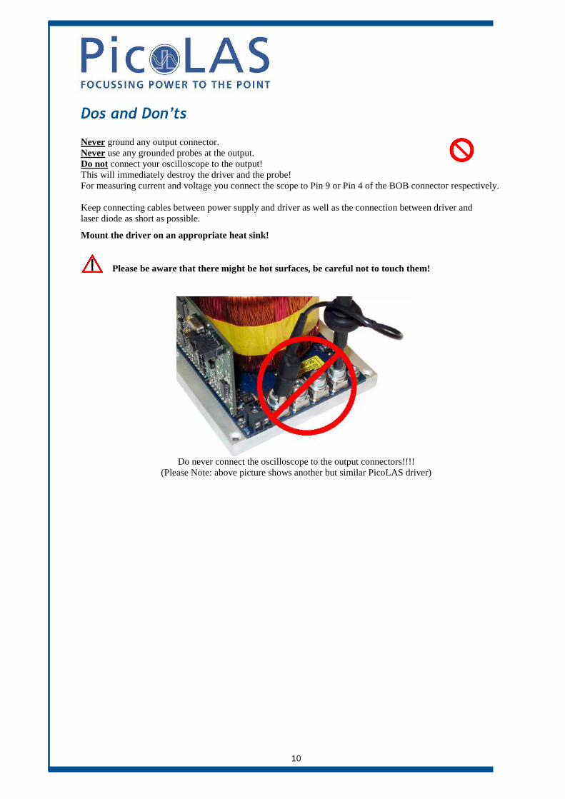
Dos and Don’ts Never ground any output connector. Never use any grounded probes at the output. Do not connect your oscilloscope to the output! This will immediately destroy the driver and the probe! For measuring current and voltage you connect the scope to Pin 9 or Pin 4 of the BOB connector respectively. Keep connecting cables between power supply and driver as well as the connection between driver and laser diode as short as possible.
Mount the driver on an appropriate heat sink!
Please be aware that there might be hot surfaces, be careful not to touch them!
Do never connect the oscilloscope to the output connectors!!!!
(Please Note: above picture shows another but similar PicoLAS driver)

11
Functional Description The driver uses a DC-DC converter to load a capacitor bank to a defined voltage. A PI regulator uses T1 and a shunt to control the current flow through the laser diode.
Laser diode current and compliance voltage are pre-processed and fed to the external BOB-connector.
Several security features protect the laser diode and driver from damage. D1 protects the laser diode from reverse currents. The switch S1 is automatically opened when an over current as well as an internal failure (such as over temperature, etc.) is detected.
Operation Principle of LDP-QCW driver
Element Function
C1 Input Buffer Capacitor
Cb Capacitor bank
S1 Security Switch
D1 Laser diode protection diode
T1 Current regulation MosFET
Shunt LD-current monitor

12
Trigger modes The LDP-QCW supports four different trigger modes, as explained below
Internal (trgmode = 0) The pulse generation is performed by an internal pulse generator. The pulse width and repetition rate is user configurable via the serial interface.
The following diagram shows an example of generated pulses. The lower graph shows the internal pulse generator, the upper two graphs the trigger pulses generated out of it.
meaning
T1 enabling of the output
T1-T2 The delay between output enable and the first generated pulse depends on the configured repetition rate. It nearly equals the pulse pause time.
T2-T3 Pulse rise time. It depends on the load inductance.
T4-T5 Pulse fall time. It depends on the load inductance.
T6 disabling of the output
T7 re-enabling of the output

13
External (trgmode = 1) The pulse generation is performed by an external pulse generator connected to the pulse input on the BOB connector. The pulses can be inverted by setting the TRG_EDGE bit in the LSTAT register to “0”.
The following diagram shows an example of generated pulses. The lower graph shows the external pulse input, the upper two graphs the trigger pulses generated out of it.
meaning
T1 enabling of the output
T2-T3 Pulse rise time. It depends on the load inductance.
T4-T5 Pulse fall time. It depends on the load inductance.
T6 disabling of the output
T7 re-enabling of the output

14
External controlled (trgmode = 2) This trigger mode uses the external trigger input to control the internal pulse generator. It is used to generate a number of pulses per rising of falling edge of the external trigger input. Setting the TRG_EDGE bit in the LSTAT register to “1” uses the rising edge, setting it to “0” uses the falling edge.
The number of pulses and the repetition rate can be set via software.
The following diagram shows an example of generated pulses. The lower graph shows the external pulse input, the upper two graphs the trigger pulses generated out of it.
meaning
T1 enabling of the output
T2-T3 Pulse rise time. It depends on the load inductance.
T4-T5 Pulse fall time. It depends on the load inductance.
T6 disabling of the output
T7 re-enabling of the output
Software (trgmode = 3) This trigger mode works exactly like the external controlled mode. The only difference is that the trigger is given using a software command.

15
Regulator The LDP-QCW implements a proportional – integral (PI) regulator to control the current flow through the connected load. The following diagram shows a simplified layout:
Depending of the chosen operating mode the user has the possibility to modify all relevant parameters to a specific need. This is done through the digital interface (PLB-21 or RS232). The proportional part of the regulator is not user accessible. The “I” value defines the strength of the integral part of the current regulator. This value ranges from 0 to 4095. A recommended value for normal operation is 30 … 60. If this value is too high it may lead to a current overshoot. PicoLAS implemented an active nonlinearity compensation of the output stage. This speeds up the device, prevents excessive current overshoots and yields a better accuracy with high impedance loads. The influence of this part of the regulator can be user defined and is called FFwd. However, the interconnection between the voltage and the current flow on the output is calibrated during fabrication. This is used in operating mode 1. So it is not necessary to change this value at all. If needed, it can be adjusted between the values 0 to 7.5 by the customer.
Be careful if changes are performed with the FFwd-value. The effect is high and may cause damage if not adjusted properly. Wrong settings are not covered by warranty.
Mode 0: manual In this operation mode all parameters can be modified.
This mode is recommended only for experienced users as any wrong setting may lead to a current overshoot at the output.
Mode 1: semi-auto In this operation mode the feed forward value is automatically chosen in dependence of the current setpoint. This is recommended for normal operation as it guarantees no current overshoot at the output. The P and I values can be freely chosen, but the default values are sufficient for most applications.
Over current protection The driver is equipped with software controllable over current protection. The user must configure a current value at witch the driver will disable itself. This is an absolute value, hence if the set point current is set to a greater value than the over current protection, the driver will generate only a partial pulse.

16
VCap The VCap value defines the voltage of the capacitor bank (see chapter functional description). This value is a bit tricky to determine as it depends on the chosen pulse width, repetition rate and compliance voltage. If his value is too low the current will drop during the pulse or not even reach the set point, if it is too high the output stage will heat up fast and lead to an over temperature shutdown. The following equation can be used to calculate the capacitor voltage in dependence of the output current, compliance voltage and pulse width:
))112.0
011.0((5pulse
LDLDcapT
IUV +++=
where LDU = compliance voltage LDI = current setpoint
pulseT = pulse width This equation does not use the repetition rate. Hence this value must be increased if a current drop is measured during operation. For first tests or low pulse width and repetition rate it can safely be set to maximum, but the higher this value the greater the power losses are in the output stage.
Max. Compliance Voltage
0
5
10
15
20
25
30
100
300
500
700
900
1100
1300
1500
1700
1900
2100
2300
2500
2700
2900
3100
3300
3500
3700
3900
4100
4300
4500
4700
4900
Pulsdauer in µs
Com
plia
nce
in V 100 A
200 A
300 A
400 A

17
LED codes The LDP-QCW is equipped with a red and a green status LED. The red LED is connected to the Pulser_ok pin of the BOB connector and will lit if the signal goes low. The green LED the following codes:
Permanent on: The LDP-QCW operates normally and the current output is enabled Blink 1x: Master Enable is given, but Enable not Blink 2x: Master Enable is not given
Power Supply To obtain a good pulsing performance with the driver, it requires an appropriate power supply unit (PSU). The PSU has to supply not only the power that is delivered to the laser diode but also the power to compensate for the losses in the driver itself.
The device is equipped with a buck-boost DC-DC converter which allows it to generate a capacitor voltage that is higher than the input voltage.
Cooling The maximum thermal dissipation of the LDP-QCW depends on the configured pulse length, repetition rate and capacitor bank voltage. For optimal cooling the base plate must be mounted to an appropriate heat sink or water cooling. The LDP-QCW is equipped with two cooling fans. They are only for cooling of the internal capacitors and are not sufficient enough to cool the whole device. It is possible to control the speed of the fans via software by disabling the automatic fan speed control. If the cooling is insufficient, the device will detect an over temperature condition and will disable itself if necessary.
Test Load A common method to test the driver is to connect a regular silicon rectifier diode to the driver output. Here has to be paid attention to the junction capacitance of the diode. Only fast recovery diodes (or similar) have a low parasitic capacitance as laser diodes. To achieve reasonable test results, the parasitic elements of the test diode and the connection must be very similar to a laser diode approach. Regular silicon rectifier diodes have a junction capacitance of several microfarads and are not a suitable test load! The use of these diodes will yield in incorrect current measurement at the pulse edges!
It is also possible to test the driver using a shortcut. This will not damage it, but result in an incorrect measurement for the rise and fall time of the current pulse.
18
Over Temperature Shutdown To protect the Laser Diode and the driver itself, the LDP-QCW automatically disables itself if its temperature rises above the maximum allowed operating temperature. This condition is latched and the LDP-QCW will not start working until temperature drops five degrees and the ENABLE-pin is toggled. During the over temperature shutdown, the Pulser_ok output (Pin 1 of the BOB-Connector) is pulled low.
Absolute Maximum Ratings
Output current 50 … 300A
Max. compliance voltage 12V (short-circuit proof)
Min. pulse duration < 100us
Max. pulse duration 5 ms
Max. repetition rate > 1 KHz
Max. duty cycle 10%
Max. rise time < 10us
Current overshoot < 5% (depending on regulator settings)
Pulse trigger input 5V TTL
external current setting input 200 A/V
Current monitor 200 A/V
Connectivity LDP-C BOB
PLB-21
Supply voltage 24 … 48V
Max. power dissipation TBD
Dimensions in mm 100 x 180 x 100
Weight 1.2 Kg
Operating temperature 0 to +55°C

19
Mechanical Dimensions The following dimensions are in millimetres (mm).
A 100 a 6
B 94 b 4,5
C 74 c 19
D 55 d 27
E 17 e 169
F 6 f 174
G 31,7 g 180
H 43,8
I 55,9
J 68

20
Controlling the LDP-QCW using a PLB-21 To control the LDP-QCW with a PLB-21 it must be connected via the enclosed cable. When the PLB-21 is connected the first time to a LDP-QCW you are asked to download a new driver. This must be confirmed with “yes” for working the PLB-21 properly.
Menu Structure The following diagram shows the structure of the PLB-21 menu which affects the LDP-QCW. All entries are described in detail. All other menu entries are described in the PLB-21 manual. For detailed instructions see the PLB-21 manual. Menu root
- Main Puls o MP Current o FFwd o I-Delay o I
- Pulsgen o MP Width o Reprate
- Trigger
o Mode o Edge o Count
- Config o Mode o Cur. stp. o OverCur F1 o Voltage
- Temperature
o Temp1 o Temp2 o Temp3 o Temp4
- Defaults
o Autoload o Save o Load

21
Main Puls
MP Current This value defines the pulse current for the next pule.
FFwd This value represents the feed forward voltage of the current regulator. See chapter current regulator for more information. I-Delay This value represents the switching-point of the integral part of the current regulator. It is defined in percent of the setpoint current. See chapter current regulator for more information.
I This value defines the strength of the integral part of the current regulator. The value ranges from 0 to 4095.
Pulsgen
MP Width This value defines the pulse width of the output pulses. This is not available in every trigger mode. Please see chapter trigger for more information.
Reprate This value defines the repetition rate of the output pulses. This is not available in every trigger mode. Please see chapter trigger for more information.
Trigger
Mode This setting defines which trigger input / mode is used. Please see chapter trigger for more information.
Edge This setting defines which edge / polarity is used for the trigger. This is not available in every trigger mode. Please see chapter trigger for more information.
Count This setting defines the number of pulses generated per trigger event. This is not available in every trigger mode. Please see chapter trigger for more information.
Config
Mode In this menu point the operation mode of the LDP-QCW can be selected. See chapter “current regulator” for more information. Cur. stp. The LDP-QCW can be configured to use the internal or external set point current. If switched to external, an appropriate voltage must be applied to the BOB connector.
OverCur If enabled, the LDP-QCW disables automatically if the current flow reaches the given value.
Voltage This value represents the precharge voltage of the current regulator. See chapter current regulator for more information.

22
Temperature
The LDP-QCW is equipped with several temperature sensors. In this submenu, the actual and shutdown temperatures can be read and modified. All values are in °C.
Temp 1…4 This shows the actual temperatures measured by the sensors of the LDP-QCW.
Defaults
def. pwron If enabled the LDP-QCW loads default values every time it is powered on. These values are CRC checked at power-up. If this check fails the values are not loaded and an error message is displayed.
Save defaults When the Jogdail is turned or the ENTER key is pressed all current values are saved.
Load defaults When the Jogdail is turned or the ENTER key is pressed all current values are overwritten by the saved ones. If the output was enabled at this time it becomes disabled.
If an Error Occurs If an error occurs during operation the pulse output is switched off, the “pulser_ok_ext” signal on the BOB connector is pulled low and a message is displayed on the PLB-21. If no other action is described on the display, a toggle of the ENABLE pin resets the error condition.
23
Controlling the LDP-QCW via RS232
Introduction The RS232 interface allows communications over a serial text interface as well as using the PicoLAS protocol. While the text interface is designed for communication with a terminal program, the PicoLAS protocol is designed as a system interact protocol.
The switching between the two protocols occurs automatically as soon as the LDP-QCW receives a certain sequence. The corresponding commands are:
• PING for the PicoLAS protocol
• “ init ” followed by <Enter> for the text interface
The connection settings are:
Baud rate 115200
Data bits 8
Stop bits 1
Parity even

24
The Serial Text Interface The following section describes the structure and commands of the text interface.
Structure Every command that is sent to the LDP-QCW must be completed with a CR (Enter). It consists of a command word followed by one ore more a parameters. If the command was successfully executed a “00” is sent, otherwise a “01”. If there is an error pending, the response will be “10”, otherwise “11”. If the command requires an answer parameter, this parameter is sent before the confirmation is given.
Example:
The user would like to read out the actual setpoint current:
User input: gcurrent<Enter>
Output of the LDP-CW: 250<CR><LF>
00<CR><LF>
Example 2:
The user would like to set a new setpoint current:
User input: scurrent 270<Enter>
Output of the LDP-CW: 270<CR><LF>
00<CR><LF>
Input is done in ASCII code and is case sensitive. Every terminal can be used that supports this standard.

25
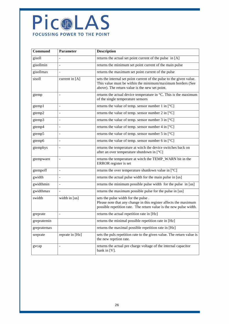
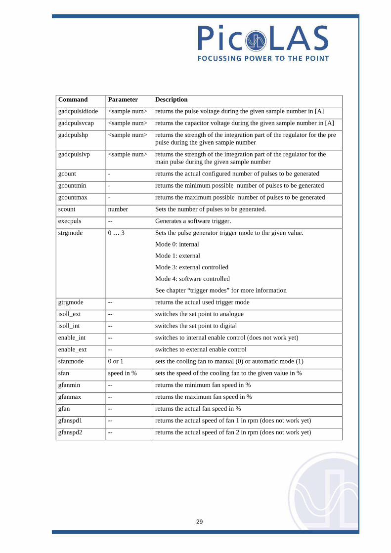
Commands for the LDP-QCW The following table contains a command reference for the LDP-QCW.
Command Parameter Description
ghwver - returns the hardware version number
gswver - returns the software version number
gserial - returns the serial number
gname - returns the device name
ps - prints out all settings
loaddef - load default values
savedef - save all settings as default values
enautodef - enables the automatic loading of default settings on power on
disautodef - disables the automatic loading of default settings on power on
gerrtxt - returns the error register in text-form
gerr - returns the error register as a 32bin number
glstat - returns the laser status register
slstat 32bit number sets the laser status register to the given value.
gtrgedge - returns “0” for negative edge or “1” for positive edge
strgedge 0 or 1 sets the trigger edge for external trigger.“0” = negative, “1” = positive
gmode - returns the current regulator mode.
Mode 0: manual
Mode 1: semi-automatic
See chapter “current regulator” for more information
smode 0 … 1 sets the current regulator mode to the given value.
Mode 0: manual
Mode 1: semi-automatic
See chapter “current regulator” for more information
26
Command Parameter Description
gisoll - returns the actual set point current of the pulse in [A]
gisollmin - returns the minimum set point current of the main pulse
gisollmax - returns the maximum set point current of the pulse
sisoll current in [A] sets the internal set point current of the pulse to the given value. This value must be within the minimum/maximum borders (See above). The return value is the new set point.
gtemp - returns the actual device temperature in °C. This is the maximum of the single temperature sensors
gtemp1 - returns the value of temp. sensor number 1 in [°C]
gtemp2 - returns the value of temp. sensor number 2 in [°C]
gtemp3 - returns the value of temp. sensor number 3 in [°C]
gtemp4 - returns the value of temp. sensor number 4 in [°C]
gtemp5 - returns the value of temp. sensor number 5 in [°C]
gtemp6 - returns the value of temp. sensor number 6 in [°C]
gtemphys - returns the temperature at witch the device switches back on after an over temperature shutdown in [°C]
gtempwarn - returns the temperature at witch the TEMP_WARN bit in the ERROR register is set
gtempoff - returns the over temperature shutdown value in [°C]
gwidth - returns the actual pulse width for the main pulse in [us]
gwidthmin - returns the minimum possible pulse width for the pulse in [us]
gwidthmax - returns the maximum possible pulse for the pulse in [us]
swidth width in [us] sets the pulse width for the pulse . Please note that any change in this register affects the maximum possible repetition rate. The return value is the new pulse width.
greprate - returns the actual repetition rate in [Hz]
grepratemin returns the minimal possible repetition rate in [Hz]
grepratemax returns the maximal possible repetition rate in [Hz]
sreprate reprate in [Hz] sets the puls repetition rate to the given value. The return value is the new reprtion rate.
gvcap - returns the actual pre charge voltage of the internal capacitor bank in [V].

27
Command Parameter Description
gvcapmin - returns the minimum pre charge voltage of the internal capacitor bank in [V]
gvcapmax - returns the maximum pre charge voltage of the internal capacitor bank in [V]
svcap voltage in [V] sets the pre charge voltage of the internal capacitor bank to the given value in [V]. One position after decimal point is used (e.g. 12.5)
gidelay - returns the delay value to witch the output current of the pulse must rise before the integral part of the current regulator is switched on. This value is measured in percent of the set point current.
sidelay delay in % sets the delay value to witch the output current of the pulse must rise before the integral part of the current regulator is switched on to the given value. This value is measured in percent of the set point current.
gidelaymin - returns the minimum i-delay value
gidelaymax - returns the maximum i-delay value
gi - returns the actual strength of the integral part of the current regulator for the pulse.
si value sets the strength of the integral part of the current regulator for the pulse to the given value.
gimin - returns the minimum strength of the integral part of the current regulator.
gimax - returns the maximum strength of the integral part of the current regulator.
gffwd - returns the actual voltage of the feed-forward part of the current regulator for the main pulse in [V]. See chapter “Current regulator” for more information.
sffwd voltage in [V] sets the feed-forward voltage for the pulse to the given value. Two positions after decimal point are used (e.g. 3.45). It must be within the borders of gffwdmin / gffwdmax.

28
Command Parameter Description
gffwdmin - returns the minimum possible value of the feed-forward voltage in [V]
gffwdmax - returns the maximum possible value of the feed-forward voltage in [V]
gocur - returns the actual over current shutdown value in [A]. The output will be disabled when the output current reaches this value. Please note that this function must be enabled to use it.
gocurmin - returns the minimum possible over current shutdown value in [A]
gocurmax - returns the maximum possible over current shutdown value in [A]
socur current in [A] sets the over current shutdown value to the given value in [A]. The output will be disabled when the output current reaches this value. Please note that this function must be enabled to use it.
enocur - enables the over current protection
disocur - disables the over current protection
gadcudiode - returns the actual measured pulse current in [A]
gadcidiode - returns the actual measured pulse voltage in [V]
gadcvcap - returns the actual measured capacitor bank voltage in [V]
gadcuin - returns the actual measured input voltage in [V]
gadcisollhp - returns the actual measured analogue set point for the main pulse
gadcnum - returns the number of samples that was taken during the last generated pulse
gadcpulsudiode <sample num> returns the pulse current during the given sample number in [A]
29
Command Parameter Description
gadcpulsidiode <sample num> returns the pulse voltage during the given sample number in [A]
gadcpulsvcap <sample num> returns the capacitor voltage during the given sample number in [A]
gadcpulshp <sample num> returns the strength of the integration part of the regulator for the pre pulse during the given sample number
gadcpulsivp <sample num> returns the strength of the integration part of the regulator for the main pulse during the given sample number
gcount - returns the actual configured number of pulses to be generated
gcountmin - returns the minimum possible number of pulses to be generated
gcountmax - returns the maximum possible number of pulses to be generated
scount number Sets the number of pulses to be generated.
execpuls -- Generates a software trigger.
strgmode 0 … 3 Sets the pulse generator trigger mode to the given value.
Mode 0: internal
Mode 1: external
Mode 3: external controlled
Mode 4: software controlled
See chapter “trigger modes” for more information
gtrgmode -- returns the actual used trigger mode
isoll_ext -- switches the set point to analogue
isoll_int -- switches the set point to digital
enable_int -- switches to internal enable control (does not work yet)
enable_ext -- switches to external enable control
sfanmode 0 or 1 sets the cooling fan to manual (0) or automatic mode (1)
sfan speed in % sets the speed of the cooling fan to the given value in %
gfanmin -- returns the minimum fan speed in %
gfanmax -- returns the maximum fan speed in %
gfan -- returns the actual fan speed in %
gfanspd1 -- returns the actual speed of fan 1 in rpm (does not work yet)
gfanspd2 -- returns the actual speed of fan 2 in rpm (does not work yet)

30
If an Error Occurs If an error occurs during operation the pulse output is switched off and the return value of a command is no longer “00” or “01” but “10” or “11”. Errors have to be acknowledged with a toggle of the ENABLE signal, otherwise switching on again of pulse output is not possible. To retrieve the error, use the gerror command for the content of the ERROR register or the gerrtxt command for a human readable form.

31
The PicoLAS Protocol The following section describes the structure and possible commands of the PicoLAS protocol.
Structure Each transmission consists of 12 bytes – called a frame as follows – which must be sent consecutively. Otherwise the system times out and the transmission must start again from the beginning.
A frame has a fixed structure. The first two bytes describe the command, the following eight bytes the parameters, followed by one reserved byte and one checksum byte. The checksum is calculated out of the first 11 bytes which are linked by a bitwise XOR.
Thus a frame has the following structure:
Byte Meaning
1 Bit 8-15 of the command
2 Bit 0-7 of the command
3 Bit 56-63 of the parameter
4 Bit 48-55 of the parameter
5 Bit 40-47 of the parameter
6 Bit 32-39 of the parameter
7 Bit 24-31 of the parameter
8 Bit 16-23 of the parameter
9 Bit 8-15 of the parameter
10 Bit 0-7 of the parameter
11 Reserved, always 0x00
12 Checksum
A properly received frame must be acknowledged by the recipient with an answer, which is also a frame. If the acknowledgement does not occur the command has not been processed and the sending procedure should be repeated.
If the recipient recognizes the command as valid, but not the parameters, then it will answer with an ILGLPARAM (0xFF12) as command.
In case that the recipient receives an invalid command it will answer with UNCOM (0xFF13).
If a faulty checksum is recognized then the answer is RXERROR (0xFF10). If this error occurs often the connection should be checked.
Using the REPEAT (0xFF11) command the recipient can instruct the sender to send the most recent frame again.

32
General Commands The following list contains an overview of the general commands which are supported by every product from PicoLAS which makes use of this protocol. The explanation of the individual commands is given further below.
PING This command is used to determine the presence of a connected device and to initialize the interface. It has no effect on the condition of the recipient. The command parameter is always zero, the answer parameter too.
IDENT It is used to determine the device ID of an attached recipient. Has no effect on the condition of the recipient. The parameter is always 0. The answer contains the ID.
GETHARDVER This command instructs the recipient to send back the version number of the hardware being used. The parameter is always zero. The answer contains the hardware version of the recipient. The format of the answer is: 0x000000<major><minor><revision>. In other words, one byte for each of the three elements of the version number. As example, version 1.2.3 has the parameter 0x000000010203.
GETSOFTVER Instructs the recipient to send back the version number of the software being used. The parameter is always 0. The answer contains the software version of the recipient. The format of the answer is: 0x000000<major><minor><revision>. In other words, one byte for each of the three elements of the version number. As example, version 2.3.4 has the parameter 0x000000020304.
GETSERIAL Instructs the recipient to send back its serial number. If 0 is sent as parameter, the answer contains the number of (ASCII) digits of the serial number; otherwise the respective position of the serial number is sent in ASCII format.
GETIDSTRING Instructs the recipient to send back the name of the device. If 0 is sent as parameter, the answer contains the number of digits of the string, otherwise the respective position of the serial number is sent in ASCII format.
Command Name Sent Frame Answer Frame
Command Parameter Command Parameter
PING 0xFE01 0 0xFF01 0
IDENT 0xFE02 0 0xFF02 ID
GETHARDVER 0xFE06 0 0xFF06 Version
GETSOFTVER 0xFE07 0 0xFF07 Version
GETSERIAL 0xFE08 0 … 255 0xFF08 Refer to description
GETIDSTRING 0xFE09 0 … 255 0xFF09 Refer to description

33
In addition to these commands there are some answers, which can be given to every command:
RXERROR If a frame is repeated four times and still broken this answer will be send.
REPEAT The last frame was received in a broken state. The transmission must be repeated. This can be up to four times before a RXERROR will be send.
ILGLPARAM The parameter of the last frame had an incorrect value.
UNCOM The command of the last frame is unknown by the device.
Answer Answer Frame
Command Parameter
RXERROR 0xFF10 0
REPEAT 0xFF11 0
ILGLPARAM 0xFF12 0
UNCOM 0xFF13 0

34
Commands for the LDP-QCW The following table contains a list of the commands which the LDP-QCW supports in addition to the generally applicable commands. An explanation of each individual command follows afterwards.
Command Sent Frame Received Frame
Command Parameter Command Parameter
GETTEMP 0x1 0 0x100 temperature in 1/10°C
GETTEMP1 0x2 0 0x100 temperature in 1/10°C
GETTEMP2 0x3 0 0x100 temperature in 1/10°C
GETTEMP3 0x4 0 0x100 temperature in 1/10°C
GETTEMP4 0x5 0 0x100 temperature in 1/10°C
GETTEMPOFF 0x6 0 0x100 temperature in 1/10°C
GETTEMPHYS 0x8 0 0x100 temperature in 1/10°C
GETLSTAT 0x10 0 0x110 32bit number
SETLSTAT 0x11 32bit number 0x110 32bit number
GETERROR 0x20 0 0x120 32bit number
GETWIDTH 0x35 0 0x130 width in [us]
GETWIDTHMIN 0x36 0 0x130 minimum width in [us]
GETWIDTHMAX 0x37 0 0x130 maximum width in [us]
SETWIDTH 0x38 width in [us] 0x130 width in [us]
GETREPRATE 0x39 0 0x130 reprate in [Hz]
GETREPRATEMIN 0x3A 0 0x130 reprate in [Hz]
GETREPRATEMAX 0x3B 0 0x130 reprate in [Hz]
SREPRATE 0x3C repare in [Hz] 0x130 reprate in [Hz]
GETCOUNT 0x3D 0 0x130 number of pulses
SETCOUNT 0x3E number of pulses 0x130 number of pulses
EXECPULSE 0x3F 0 0x130 executes a software trigger
GETFFWD 0x42 0 0x140 voltage in 1/100V
SETFFWD 0x43 voltage in 1/100V 0x140 voltage in 1/100V
GETFFWDMIN 0x44 0 0x140 minimum voltage in 1/100V
GETFFWDMAX 0x45 0 0x140 maximum voltage in 1/100V
GETCAP 0x50 0 0x150 voltage in 1/10V
GETCAPMIN 0x51 0 0x150 minimum voltage in 1/10V

35
Command Sent Frame Received Frame
Command Parameter Command Parameter
GETCAPMAX 0x52 0 0x150 maximum voltage in 1/10V
SETCAP 0x53 voltage in 1/10V 0x150 voltage in 1/10V
GETI 0x62 0 0x160 strength of I
SETI 0x63 strength of I 0x160 strength of I
GETIMIN 0x64 0 0x160 minimum I value
GETIMAX 0x65 0 0x160 maximum I value
GETCUR 0x74 0 0x170 current in [A]
GETCURMIN 0x75 0 0x170 minimum current in [A]
GETCURMAX 0x76 0 0x170 maximum current in [A]
SETCUR 0x77 current in [A] 0x170 current in [A]
GETOCUR 0x80 0 0x180 current in [A]
GETOCURMIN 0x81 0 0x180 minimum current in [A]
GETOCURMAX 0x82 0 0x180 maximum current in [A]
SETOCUT 0x83 current in [A] 0x180 current in [A]
GETIDELAY 0x92 0 0x190 delay in 1/10%
SETIDELAY 0x93 delay in 1/10% 0x190 delay in 1/10%
GETIDELAYMIN 0x94 0 0x190 minimum delay in 1/10%
GETIDELAYMAX 0x95 0 0x190 maximum delay in 1/10%
LOADDEFAULTS 0xB0 0 0x1B0 0 (see below)
SAVEDEFAULTS 0xB1 0 0x1B0 0 (see below)
GETADCUDIODE 0xC0 0 0x1C0 output voltage in 1/10V
GETADCIDIODE 0xC1 0 0x1C0 output current in [A]
GETADCVCAP 0xC2 0 0x1C0 capacitor voltage in 1/10V
GETADC5V 0xC3 0 0x1C0 internal 5V in 1/10V

36
Command Sent Frame Received Frame
Command Parameter Command Parameter
GETADCUIN 0xC5 0 0x1C0 input voltage in 1/10V
GETADCISOLL 0xC6 0 0x1C0 external set point current for pre pulse in [A]
GETADCPULSSAMPLES 0xC7 0 0x1C0 see below
GETADCPULSIDIODE 0xC8 see below 0x1C0 output current in [A]
GETADCPULSUDIODE 0xC9 see below 0x1C0 output voltage in 1/10V
GETADCPULSVCAP 0xCA see below 0x1C0 capacitor voltage in 1/10V
GETADCPULSIVP 0xCB see below 0x1C0 see below
GETADCPULSIHP 0xCC see below 0x1C0 see below
GETFAN 0xD0 0 0x1D0 fan speed in %
GETFANMIN 0xD1 0 0x1D0 minimum fan speed in %
GETFANMAX 0xD2 0 0x1D0 maximum fan speed in %
SETFAN 0xD3 fan speed in % 0x1D0 fan speed in %
GETFANSPEED1 0xD4 0 0x1D0 fan speed in rpm
GETFANSPEED2 0xD5 0 0x1D0 fan speed in rpm

37
Description of the Individual Commands
GETTEMP Returns the maximum of the GETTEMP1 … GETTEMP4 commands. The value is encoded as a signed integer (16bit), measured in steps of 0.1°C.
GETTEMP1…4 Returns the measured value of the according temperature sensor. The value is encoded as a signed integer (16bit), measured in steps of 0.1°C.
GETTEMPOFF Returns the temperature border at which the device shuts down automatically. The value is encoded as a signed integer (16bit), measured in steps of 0.1°C.
GETTEMPHYS Returns the temperature to which the device must cool down until it can be switched on again. The value is encoded as a signed integer (16bit), measured in steps of 0.1°C.
GETLSTAT Returns the content of the laser status register (32bit). For a detailed description of the single bits see chapter “description of the LSTAT register”.
SETLSTAT Sets the laser status register to the given value. The return value contains the acquired register content. For a detailed description of the single bits see chapter “description of the LSTAT register”.
GETERROR Returns the content of the error register (32bit). For a detailed description of the single bits see chapter “description of the ERROR register”.
GETWIDTH Returns the actual pulse width of the pulse. The value is measured in [us].
GETWIDTHMIN Returns the minimum possible pulse width of the pulse. The value is measured in [us].
GETWIDTHMAX Returns the maximum possible pulse width of the pulse. This value depends of the current repetition rate. Hence, any change in the repetition rate changes this value too. It is measured in [us].
SETWIDTH Sets the pulse width of the pulse generator to the given value. It must be within the borders defined by GETWIDTHHPMIN and GETWIDTHHPMAX. The value is measured in [us].
GETREPRATE Returns the actual pulse repetition rate of the internal pulse generator. The value is measured in [Hz].
GETREPRATEMIN Returns the minimum possible pulse repetition rate of the internal pulse generator. The value is measured in [Hz].

38
GETREPRATEMAX Returns the maximum possible pulse repetition rate of the internal pulse generator. The value is measured in [Hz].
SETWIDTH Sets the pulse repetition rate of the pulse generator to the given value. It must be within the borders defined by GETREPRATEMIN and GETREPRATEMAX. The value is measured in [Hz].
GETCOUNT Returns the number of pulses that will be generated with a given trigger. This is only used in trigger modes 2 and 3.
SETCOUNT Sets the number of pulses that will be generated with a given trigger to the given value. This is only used in trigger modes 2 and 3. The value must be within 1 and 1000000.
GETFFWD Returns the actual feed forward voltage used by the pulse current regulator. See chapter “current regulator” for more information. It is measured in steps of 0.01[V]
SETFFWD Sets the feed forward voltage used by the pulse current regulator to the given value. It must be within the borders defined by GETFFWDMIN and GETFFWDMAX. See chapter “current regulator” for more information. The value is measured in steps of 0.01[V]
GETFFWDMIN Returns the minimal feed forward voltage used by the current regulator. It is measured in steps of 0.01[V]
GETFFWDMAX Returns the maximal feed forward voltage used by the current regulator. It is measured in steps of 0.01[V]
GETCAP Returns the actual pre charge voltage of the capacitor bank. See chapter “current regulator” for more information. It is measured in steps of 0.1[V]
GETCAPMIN Returns the minimal pre charge voltage of the capacitor bank. It is measured in steps of 0.1[V]
GETCAPMAX Returns the maximal pre charge voltage of the capacitor bank. It is measured in steps of 0.1[V]
SETCAP Sets the pre charge voltage of the capacitor bank to the given value. It must be within the borders defined by GETCAPMIN and GETCAPMAX. See chapter “current regulator” for more information. The value is measured in steps of 0.1[V]
GETI Returns the actual strength of the integral part of the pulse current regulator. See chapter “current regulator” for more information.
39
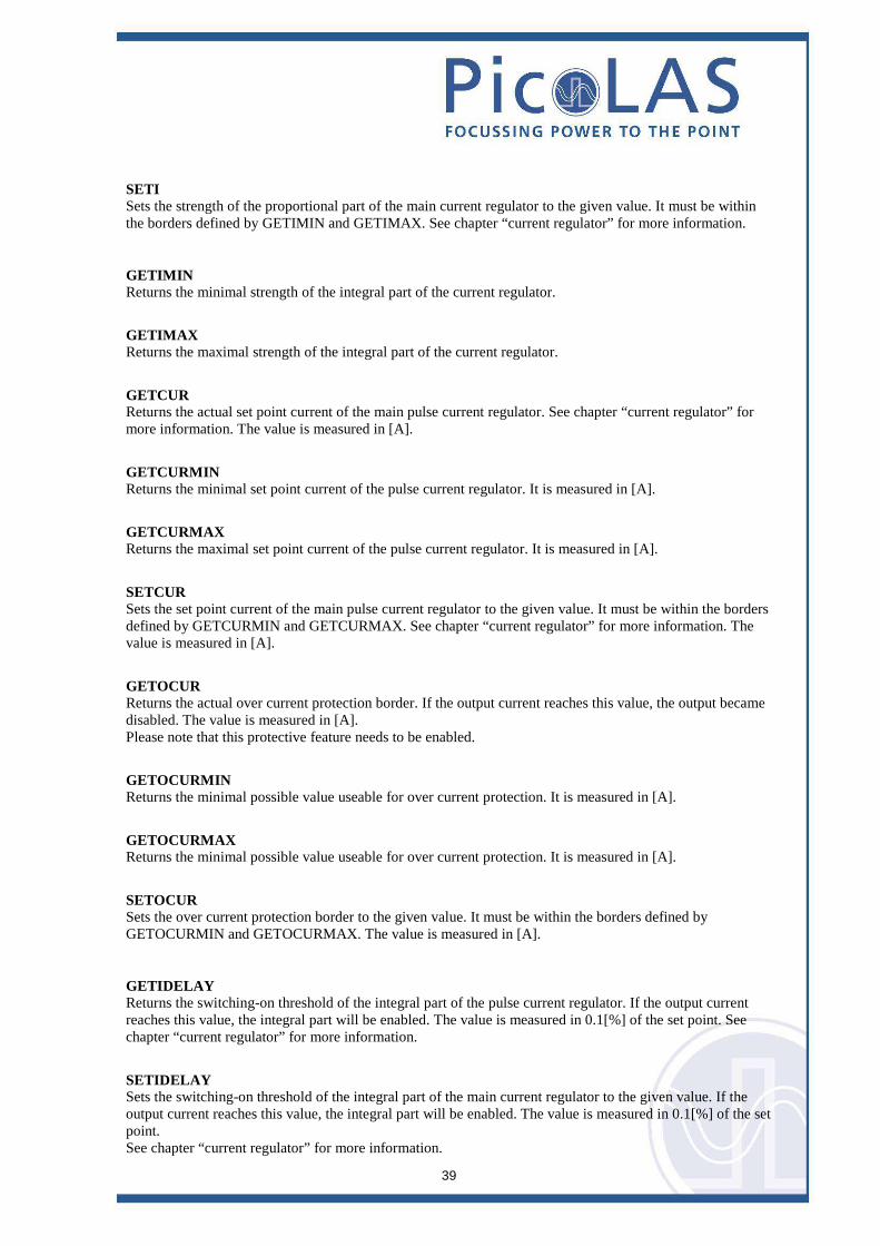
SETI Sets the strength of the proportional part of the main current regulator to the given value. It must be within the borders defined by GETIMIN and GETIMAX. See chapter “current regulator” for more information.
GETIMIN Returns the minimal strength of the integral part of the current regulator.
GETIMAX Returns the maximal strength of the integral part of the current regulator.
GETCUR Returns the actual set point current of the main pulse current regulator. See chapter “current regulator” for more information. The value is measured in [A].
GETCURMIN Returns the minimal set point current of the pulse current regulator. It is measured in [A].
GETCURMAX Returns the maximal set point current of the pulse current regulator. It is measured in [A].
SETCUR Sets the set point current of the main pulse current regulator to the given value. It must be within the borders defined by GETCURMIN and GETCURMAX. See chapter “current regulator” for more information. The value is measured in [A].
GETOCUR Returns the actual over current protection border. If the output current reaches this value, the output became disabled. The value is measured in [A]. Please note that this protective feature needs to be enabled.
GETOCURMIN Returns the minimal possible value useable for over current protection. It is measured in [A].
GETOCURMAX Returns the minimal possible value useable for over current protection. It is measured in [A].
SETOCUR Sets the over current protection border to the given value. It must be within the borders defined by GETOCURMIN and GETOCURMAX. The value is measured in [A].
GETIDELAY Returns the switching-on threshold of the integral part of the pulse current regulator. If the output current reaches this value, the integral part will be enabled. The value is measured in 0.1[%] of the set point. See chapter “current regulator” for more information.
SETIDELAY Sets the switching-on threshold of the integral part of the main current regulator to the given value. If the output current reaches this value, the integral part will be enabled. The value is measured in 0.1[%] of the set point. See chapter “current regulator” for more information.

40
GETIDELAYMIN Returns the minimal possible value useable as switching-on threshold. It is measured in 0.1[%].
GETIDELAYMAX Returns the maximal possible value useable as switching-on threshold. It is measured in 0.1[%].
LOADDEFAULTS This command replaces all internal parameters with their default values. If the output is enabled during the execution of this command, the L_ON bit of the LSTAT register will be cleared and the output disabled. This command will fail if the CRC_DEFAULT_FAIL bit in the ERROR register I set, indicating an error within the data. If the DEF_PWRON bit in the LSTAT register is set, the device automatically loads these values during power-up.
SAVEDEFAULTS This command saves all internal parameters into an EEPROM for later usage. Use command LOADDEFAULTS to restore them.
GETADCUDIODE Returns the current output voltage of the device. The value is measured in 0.1[V].
GETADCIDIODE Returns the current output current of the device. The value is measured in [A].
GETADCVCAP Returns the voltage of the capacitor bank. The value is measured in 0.1[V].
GETADCISOLL Returns the external set point current. If the ISOLL_EXT bit in the LSTAT register is set, this value is used instead of the internal one. It is measured in [A].
GETADCPULSSAMPLES Returns the number of samples taken by the LDP-QCW during the last pulse. Please see chapter “pulse measurement” for more information.
GETADCPULSIDIODE This command takes the number of the desired sample and returns the appropriate measurement value. It is measured in [A]. If an invalid sample number is given, ILGLPARAM will be send.
GETADCPULSUDIODE This command takes the number of the desired sample and returns the appropriate measurement value. It is measured in 0.1[V]. If an invalid sample number is given, ILGLPARAM will be send.
GETADCPULSVCAP This command takes the number of the desired sample and returns the appropriate measurement value. It is measured in 0.1[V]. If an invalid sample number is given, ILGLPARAM will be send.

41
GETADCPULSI This command takes the number of the desired sample and returns the appropriate measurement value. If an invalid sample number is given, ILGLPARAM will be send.
GETFAN This command returns the speed of the cooling fans in %.
GETFANMIN This command returns the minimum speed of the cooling fans in %.
GETFANMAX This command returns the maximum speed of the cooling fans in %.
SETFAN This command returns the speed of the cooling fans to the given value in %. I must be within the borders defined by GETFANMIN and GETFANMAX.
GETFANSPEED1 This command returns the speed of the cooling fan 1 in rounds pre minute (rpm). Please note that this command does not work yet.
GETFANSPEED2 This command returns the speed of the cooling fan 2 in rounds pre minute (rpm). Please note that this command does not work yet.
42
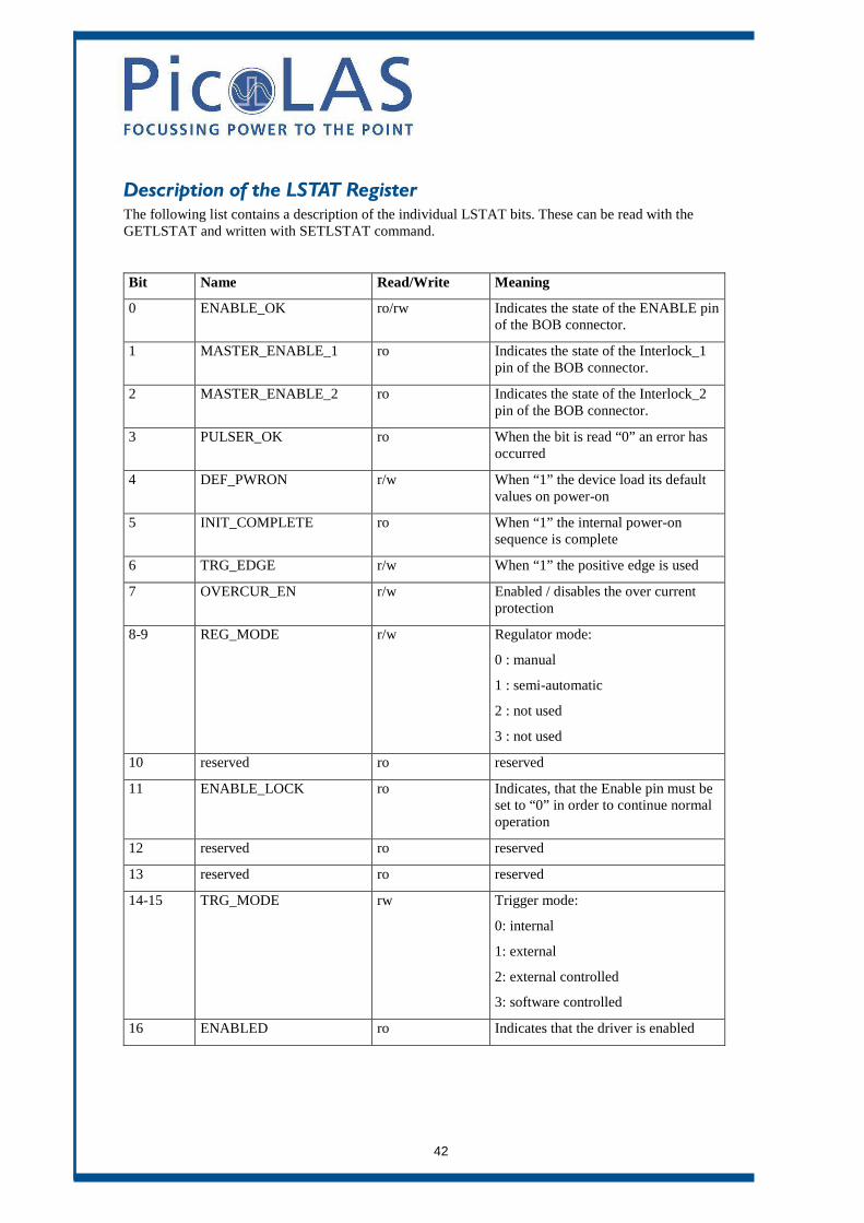
Description of the LSTAT Register The following list contains a description of the individual LSTAT bits. These can be read with the GETLSTAT and written with SETLSTAT command. Bit Name Read/Write Meaning
0 ENABLE_OK ro/rw Indicates the state of the ENABLE pin of the BOB connector.
1 MASTER_ENABLE_1 ro Indicates the state of the Interlock_1 pin of the BOB connector.
2 MASTER_ENABLE_2 ro Indicates the state of the Interlock_2 pin of the BOB connector.
3 PULSER_OK ro When the bit is read “0” an error has occurred
4 DEF_PWRON r/w When “1” the device load its default values on power-on
5 INIT_COMPLETE ro When “1” the internal power-on sequence is complete
6 TRG_EDGE r/w When “1” the positive edge is used
7 OVERCUR_EN r/w Enabled / disables the over current protection
8-9 REG_MODE r/w Regulator mode:
0 : manual
1 : semi-automatic
2 : not used
3 : not used
10 reserved ro reserved
11 ENABLE_LOCK ro Indicates, that the Enable pin must be set to “0” in order to continue normal operation
12 reserved ro reserved
13 reserved ro reserved
14-15 TRG_MODE rw Trigger mode:
0: internal
1: external
2: external controlled
3: software controlled
16 ENABLED ro Indicates that the driver is enabled

43
Bit Name Read/Write Meaning
17 reserved ro reserved
18 ISOLL_EXT rw When “1” the analogue current set point values will be used
19 EXEC_SW_PULSE rw When “1”, the driver will execute a pulse (in trigger mode 3)
20 EXECUTING_PULSES ro Indicates that the driver is currently executing a software trigger
21 ABORT_EXEC_PULSES rw When “1”, the driver will abort the current software trigger
22 Reserved ro reserved
23 Reserved ro reserved
24 FAN_AUTO rw When “1” the speed of the cooling fan is regulated automatically
25-31 Reserved ro Reserved

44
Description of the ERROR Register The following list contains a description of the individual bits of the ERROR register. A “1” as a bit leads to a deactivation of the output current.
The ERROR bits are cleared by disabling of the ENABLE pin.
Bit Name Read/Write Meaning
0 CRC_DEVDRV_FAIL ro A CRC error was detected in the PLB driver. The driver cannot be used. This does not affect the device but the PLB.
1 CRC_DEFAULT_FAIL ro A CRC error was detected in the default values. A re-save of the values should correct this.
2 CRC_CONFIG_FAIL ro A CRC error was detected in the internal configuration values. Please contact your distributor.
3 reserved ro
4 CRC_FFWDCAL_FAIL_1 ro A CRC error was detected in the internal calibration values. Please contact your distributor.
5 CRC_FFWDCAL_FAIL_2 ro A CRC error was detected in the internal calibration values. Please contact your distributor.
6 reserved ro
7 reserved ro
8 CRC_VCAPCAL_FAIL ro A CRC error was detected in the internal calibration values. Please contact your distributor.
9 OCUR_DETECTED ro The over current protection has disabled the output.
10 TEMP_OVERSTEPPED ro The internal temperature was beyond safe operating limits.
11 TEMP_WARNING ro The internal temperature is 5°C before shutdown.
12 TEMP_HYSTERESE ro Device is cooling down. Temperature needs to drop below (maximum – 10°)
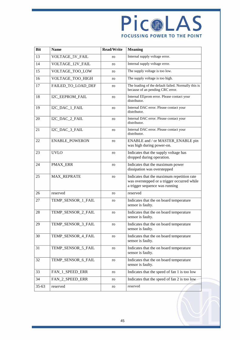
45
Bit Name Read/Write Meaning
13 VOLTAGE_5V_FAIL ro Internal supply voltage error.
14 VOLTAGE_12V_FAIL ro Internal supply voltage error.
15 VOLTAGE_TOO_LOW ro The supply voltage is too low.
16 VOLTAGE_TOO_HIGH ro The supply voltage is too high.
17 FAILED_TO_LOAD_DEF ro The loading of the default failed. Normally this is because of an pending CRC error.
18 I2C_EEPROM_FAIL ro Internal EEprom error. Please contact your distributor.
19 I2C_DAC_1_FAIL ro Internal DAC error. Please contact your distributor.
20 I2C_DAC_2_FAIL ro Internal DAC error. Please contact your distributor.
21 I2C_DAC_3_FAIL ro Internal DAC error. Please contact your distributor.
22 ENABLE_POWERON ro ENABLE and / or MASTER_ENABLE pin was high during power-on.
23 UVLO ro Indicates that the supply voltage has dropped during operation.
24 PMAX_ERR ro Indicates that the maximum power dissipation was overstepped
25 MAX_REPRATE ro Indicates that the maximum repetition rate was overstepped or a trigger occurred while a trigger sequence was running
26 reserved ro reserved
27 TEMP_SENSOR_1_FAIL ro Indicates that the on board temperature sensor is faulty.
28 TEMP_SENSOR_2_FAIL ro Indicates that the on board temperature sensor is faulty.
29 TEMP_SENSOR_3_FAIL ro Indicates that the on board temperature sensor is faulty.
30 TEMP_SENSOR_4_FAIL ro Indicates that the on board temperature sensor is faulty.
31 TEMP_SENSOR_5_FAIL ro Indicates that the on board temperature sensor is faulty.
32 TEMP_SENSOR_6_FAIL ro Indicates that the on board temperature sensor is faulty.
33 FAN_1_SPEED_ERR ro Indicates that the speed of fan 1 is too low
34 FAN_2_SPEED_ERR ro Indicates that the speed of fan 2 is too low
35-63 reserved ro reserved