itc 2015 - marvell present : "improving quality and yield through optimal+ big data...
TRANSCRIPT
NASDAQ: MRVL
Improving Quality and Yield Through Optimal+ Big Data AnalyticsInternational Test Conference
October 2015

PAGE 2© MARVELL SEMICONDUCTOR 2015 ALL RIGHTS RESERVED
Marvell at Glance
Top 5 global fabless
semiconductor company
IPO on June 27, 2000
Operating headquarters in
Santa Clara, CA, USA
Founded in 1995 by three UC
Berkeley engineers
7,000+ employees (end of
FY15)
Annual revenue of $3.7B
(end of FY15)
Approximately 1B chips
shipment per year
5,000+ patents filed and
2,500+ patents pending
A world leader in storage,
communications and
consumer semiconductor
solutions
Major R&D Centers
United States China Israel
Global Presence
India IndonesiaVietnamSingapore Taiwan Hong Kong Korea
Germany Spain U.K.Switzerland ItalyFrance DenmarkSweden
Japan

PAGE 3© MARVELL SEMICONDUCTOR 2015 ALL RIGHTS RESERVED
Delivering Diverse Product Solutions
Storage
Controllers
IP/Ethernet
NetworkingBroadband
Access
AutomotiveHome
Networking
Wireless
Connectivity
Multimedia
Entertainment
Internet of Things
(IoT)
Smart LED
Lighting
2D/3D
Printing
Power
Management
Embedded
Computing
Advanced Software Technology

PAGE 4© MARVELL SEMICONDUCTOR 2015 ALL RIGHTS RESERVED
Delivering the Industry’s Leading Solutions
#1 in market share for
HDD/SSD/Hybrid storage
controllers
1st ARM-based micro-
server storage system
#1 Ethernet access
silicon vendor
#2 IP/Ethernet networking
silicon vendor
#1 in market share (40%)
for 2D printer digital
imaging SoCs
2nd generation Android TV
HD multimedia SoC
provider

PAGE 5© MARVELL SEMICONDUCTOR 2015 ALL RIGHTS RESERVED
Marvell Supply Chain
PAGE 6© MARVELL SEMICONDUCTOR 2015 ALL RIGHTS RESERVED
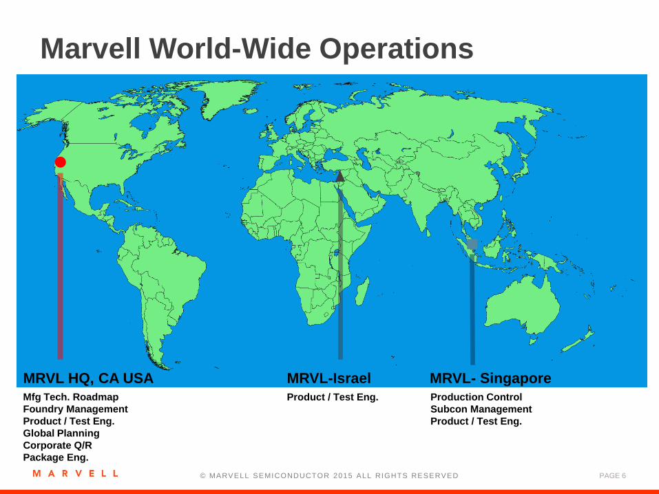
Marvell World-Wide Operations
MRVL- SingaporeMRVL HQ, CA USA MRVL-Israel
Mfg Tech. Roadmap
Foundry Management
Product / Test Eng.
Global Planning
Corporate Q/R
Package Eng.
Product / Test Eng. Production Control
Subcon Management
Product / Test Eng.

PAGE 7© MARVELL SEMICONDUCTOR 2015 ALL RIGHTS RESERVED
Operations Background (Where We Were in 2012)
• Marvell manufacturing 1B+ units per year
• Existing “systems” in place– Labor-intensive, but they were working
• The Ops team identified several areas for improvement– Faster access to manufacturing data
– Ability to drill down across all products and test domains
– Automated data analytics, plots and alerts for all devices
– Better, data-driven internal communication across company sites
– Better, data-driven external communication to subcons

PAGE 8© MARVELL SEMICONDUCTOR 2015 ALL RIGHTS RESERVED
Implemented Optimal+ In 2013
CLIENT APPLICATIONS• Analytics• Queries• Rules• Simulations
APPLICATIONSERVERS
OPTIMAL+ DATABASE
PROXY SERVER
Alerts & Linked Reports
Guidance & Requests
MES
WAFER SORT TESTER
FINAL TESTTESTER
OPERATIONS CLIENT
Marvell Subcons Marvell Headquarters

PAGE 9© MARVELL SEMICONDUCTOR 2015 ALL RIGHTS RESERVED
Optimal+ Provided Early Successes
• Yield Improvement
Manufacturing issues

PAGE 10© MARVELL SEMICONDUCTOR 2015 ALL RIGHTS RESERVED
Optimal+ Provided Early Successes
• Improvements in Throughput and Capacity

PAGE 11© MARVELL SEMICONDUCTOR 2015 ALL RIGHTS RESERVED
Unexpected Findings and Benefits
• Very little cross-company learning for subcons already
supporting Optimal+– No sharing of information about best-practices
• Optimal+ found some basic issues that should not have
been there in the production line– Despite tools in place at subcons that should have detected the problems.
• Big Data benefits that were unforeseen during pilot – Duplicate ECIDs (electronic chip IDs)
– Ugly wafers
– Improvements in “institutional knowledge”

Duplicate ECIDs

PAGE 13© MARVELL SEMICONDUCTOR 2015 ALL RIGHTS RESERVED
Serious Product Issue at EMS
• Trigger event: In early 2015, one of our customer’s EMS
reported “off the charts” DPPM for an assembly lot– Error code was related to data programmed by Marvell at the unit level
– EMS readied the units to be returned to Marvell’s FA team
• At the same time, Marvell’s Product Engineering team
reviewed the lot and manufacturing history using O+– All general indicators were normal (yield etc.)
– Product engineer did a simple “drill down” into the manufacturing data
which quickly uncovered an ECID anomaly
– 151 repeated instances of same ECID at Final Test, but not in Wafer Sort
ECID Analysis Final Test Max
Instances of ECID
Wafer Sort Max
Instances of ECID
LOT_abc_Z17 151 1
All Others 1 1

PAGE 14© MARVELL SEMICONDUCTOR 2015 ALL RIGHTS RESERVED
Rapid Identification of the Problem
• ECID Sequence Plot clearly showed an anomaly– No other repeated ECIDs observed in this Lot other than the one below
• Likely cause was a “piggybacking” event
ECID Plot in Test SequenceSame ECID repeated Sequentially
ECID
Final Test IC Touch Down Sequence

PAGE 15© MARVELL SEMICONDUCTOR 2015 ALL RIGHTS RESERVED
Root Cause Analysis
• Ops looked at the “Index Time” between each unit– Test iterations between the 2 long pauses = the # of ECID’s repeated
• Wafer Level data showed no repeated ECID– This data result is not possible without a Piggyback event
Trend Plot of Time Between TestRegion Shown: Same as repeated ECID
Error cleared here
Long pause time
No repeated ECID
Improperly dispositioned by EMS
Handler Jam occurs
Long pause time
ECID issue started here
Exactly 151 iterations

PAGE 16© MARVELL SEMICONDUCTOR 2015 ALL RIGHTS RESERVED
Key Takeaways
• Quantum improvement in debug of difficult FA– Abnormality observed within 15 minutes
– Root Cause determined in 1 hour
– Engineering work completed in <1 day, 6,000 miles from occurrence
• Risk assessment on the 4.5M units already shipped
– Corrective / Preventative Action in place 1 week after diagnosis
• Significant FA work and time saved– Mobilizing QA team
– Cycle time of doing general FA (shipping, testing, etc.)
• Automated signature detection rule was implemented to
immediately recognize this problem in the future
• All addressed using Optimal+

“Ugly Wafer” Detection using Escape Prevention

PAGE 18© MARVELL SEMICONDUCTOR 2015 ALL RIGHTS RESERVED
Escape Prevention Solution
• In early 2015, Marvell was in the process of implementing
the Optimal+ Escape Prevention solution to improve
overall product quality by reducing test escapes
• The Escape Prevention solution included 3 families of
Outlier Detection capabilities:– Parametric, Geographical & Cross-Operational
• The solution was already embedded into ALL major
foundries & OSAT operations used by Marvell
• The combination of Escape Prevention and
comprehensive production data enabled Marvell to find
expected and unexpected things

PAGE 19© MARVELL SEMICONDUCTOR 2015 ALL RIGHTS RESERVED
Expected Results: GDBN & Clusters

PAGE 20© MARVELL SEMICONDUCTOR 2015 ALL RIGHTS RESERVED
Other Expected Results: Clusters

PAGE 21© MARVELL SEMICONDUCTOR 2015 ALL RIGHTS RESERVED
Observations using Escape Prevention
• While tuning EP rules, the Marvell Ops team detected
“unusual defect patterns” on the wafers– Easy to see visually, difficult to detect algorithmically
• Marvell worked with Optimal+ to enhance our existing
algorithms to automatically identify the wafer defects that
were discovered– Fully automated process that could run on every manufactured wafer
• This finding prompted Marvell to establish a new metric
for Subcon communication: The “Ugly Wafer” metric

PAGE 22© MARVELL SEMICONDUCTOR 2015 ALL RIGHTS RESERVED
Wafers with “Unusual Defect Patterns”
Easy to identify
visually, but
hard to identify
automatically
when looking at
data with an
algorithm

PAGE 23© MARVELL SEMICONDUCTOR 2015 ALL RIGHTS RESERVED
Ugly Wafer Metric
• After realizing the number of “scratched” wafers being delivered,
Optimal+ worked with Marvell to enhance the existing algorithms to
automatically identify these “ugly wafers”
• Results are tabulated into a quantifiable metric that is used in
discussions with fabs during QBRs

PAGE 24© MARVELL SEMICONDUCTOR 2015 ALL RIGHTS RESERVED
Key Takeaways
• Automated detection of “ugly wafers.”– Run on 100% of sorted wafers
– Real time detection
– Allows quick disposition and feedback to foundry
• Throughput improvement of detection of “ugly wafers”– Marvell makes 1B units a year, 1000 wafer lots a month, lots of work if
done by hand
– Human inspection is inefficient and error prone
– Fatigue is a major factor in missing a pattern
• Completely facilitated by O+ rule implementation.

PAGE 25© MARVELL SEMICONDUCTOR 2015 ALL RIGHTS RESERVED
Better Communication

PAGE 26© MARVELL SEMICONDUCTOR 2015 ALL RIGHTS RESERVED
Improved Communications: Consistent Data Shared Internally and Externally
FinanceInventory
Billing Supply
MaterialManage-
ment
B2B
Test Data Test DataO
ps
Ac
tion
s
Ops Actions
Proxy Proxy Proxy
Factory C
Proxy Proxy Proxy
Factory B
Proxy Proxy Proxy
Factory A
Same data shared between
engineering, operations,
planners, finance and
management
Ops Actions
Te
st D
ata

PAGE 27© MARVELL SEMICONDUCTOR 2015 ALL RIGHTS RESERVED
Future Directions of Marvell

PAGE 28© MARVELL SEMICONDUCTOR 2015 ALL RIGHTS RESERVED
Driving Continuous Innovation
FLC® (Final-Level Cache)• Enables much lower-cost and lower-power systems
• Opens up new market opportunity for larger audience
• Allows Terabytes of main memory for servers
MoChi™ (MOdular CHIp)• Enables Virtual SoC (VSoC)
• Extends Moore’s Law
• Reduces development cost via reuse of functions
FLCTM (Final-Level Cache)• Significantly reduced memory size
• Optimized energy efficiency
• Reduced form factor
MoChi™ (MOdular CHIp)• Quick time-to-market
• Flexible configuration for targeted applications
• Reduced R&D cost via reusable functions

PAGE 29© MARVELL SEMICONDUCTOR 2015 ALL RIGHTS RESERVED
MoChi™ (MOdular CHIp)
Single-Die SoC
Conventional
Virtual SoC
Lego®-like concept

PAGE 30© MARVELL SEMICONDUCTOR 2015 ALL RIGHTS RESERVED
DRAM
CPU
L3 CacheL2 CacheL1 Cache
Final-Level Cache (FLCTM)
Conventional
HS-DRAM
DRAM or
RRAM
Main Memory FLCSmaller, Faster, Lower-Power DRAM
High Speed
Now Future
DRAM
Flash
CPU
L3 CacheL2 CacheL1 Cache
HS-DRAM
CPU
L3 CacheL2 CacheL1 Cache
DRAM/RRAM
Flash
Stage 1
Stage 2

Questions?

Thank You!