isscc 2014 – tutorial transcription peripheral circuits...
TRANSCRIPT
ISSCC 2014 – Tutorial Transcription Peripheral Circuits for Analog-to-Digital Converters
Instructor: Marco Corsi
1. Introduction Thank you and good morning. Over the last few years, we’ve talked about tutorial subjects in the data converter subcommittee and this particular topic has come up year after year, and finally we decided to go give this presentation, and the thing that I realized as I started to make the slides for this talk is there is effectively limitless war stories that I could talk about and so I had to limit the scope of what I was going to talk about into a few relatively simple areas to try to give you an overview or a glimpse into the horror of actually using these high performance products when you use modern data converters. Modern data converters are really truly remarkable devices; you can routinely buy ADCs that have to settle to microvolt resolution in fractions of a nanosecond, which if you were to actually even talk about that ten years ago everyone would have thought you were mad. So from that point, I’ll move forward here. So I’m going to give an overview of what peripheral circuits are and then specifically I’m going to talk about the analog interface circuits that we might use for a precision ADC, I’ll go through some design examples, and then I’ll talk a bit about the analog interface circuits that we’ll use on the inputs of high speed ADC which is a typical type of ADC used for communication channels, talk a bit about voltage references because they’re an important piece, discuss clocking and then try to come up with some sort of conclusion that ties it all together. So what’s an ADC? Okay, briefly, I’m hoping you all know what an ADC is. An ADC is an analog to digital converter. 2. Overview of Peripheral Circuits What’s an ADC, it takes an analog signal coming in and there’s a clock that feeds it so you have an input that has the precision analog signal you’re trying to convert to digital word. You have digital words coming out of it, there’s a clock going in and the clock strikes the ADC to convert the analog to a digital signal. All of these signals can affect the performance you get out of the ADC in the final application. 3. Peripheral Circuits And so analog inputs, reference, clock input, power supply, that’s what I’m going to talk about today. I didn’t talk about digital outputs, I’ll briefly talk about them at the end, they’re actually on high speed ADCs, a real headache. So my first example, I’m going to talk about a precision SAR ADC.
4. SAR ADC’s Block Diagram So many precision ADC’s that you buy from companies like TI and Analog Devices, are based on successive approximation register, and effectively what you have inside these converters is you have some sort of sample and hold amplifier. This may well be the CDAC and the CDAC is a capacitor array which you sample the signal onto by connecting arrays in different ways you can make it into a DAC and then divide the signal and compare it to a reference with a comparator. And then you go through this comparison process again and again, and again, until you resolve the final signal that the data converter converts. You have a digital interface, and you have a logic that keeps track of what’s going on and comes up with a word that represents the analog input signal. 5. Equivalent Input Circuit So what is the input look like? So typically, if you want to simplify what it looks like, generally, we have a capacitor and there’s a switch and in addition to the switch you have ESD circuits. Now generally ESD circuits aren’t analog in an AD converter, it usually consists of just diodes to the power supplies. These are generally a good way of making low capacitance relatively low distortion ESD protection. On a slow speed ADC, these diodes really don’t have much impact into the linearity because generally, they’re low leakage and within the signal range that the ADC accepts, doesn’t really have much impact. On high performance ADCs, this nonlinear capacitance that these diodes present can be a problem, for the sake of this particular ADC, the nonlinear capacitance isn’t really an issue. The biggest thing you generally need to worry about with these diodes and the switch also has diodes built into it because most ADC’s are manufactured on a junction isolated technology. If you take the analog signal outside of the power supplies, which a lot of applications can, you can potentially inject current into the substrate or through the substrate PNPs which is usually resulting with this diode. And that can cause potentially latch up issues, if the ADC is designed right, it won’t latch up, but generally you end up with some odd time constants because when you inject charge into the substrate of an IC, that charge, the minority carrier charge has very, very, long lifetimes and can get picked up by internal circuitry, even milliseconds after the event happened. Driving an ADC input outside of the power supply, can generate all sort of phenomena and generally it’s best to avoid it. Many ADC data sheets actually talk about what happens when you do that and so sometimes it’s good to put external shockley diodes on an input if your application drives it outside the supplies, because then the majority of that current will flow through the external shockleys and not cause hot time constants that you might see inside the chip.
So what does it look like? We’ve got a switch and a capacitor, and another small switch, so this might be an array of capacitors and this other switch might be many other switches. In fact this might be many other switches too. But effectively when the switch is shut, you look into an IC circuit and generally there isn’t a real resistor there, that resistor is just what switches add up to. And a capacitor in the case of this ADC, it’s a 48pF capacitor which is fairly large for a high speed circuit; this is not a particularly fast ADC. Then this switch opens, then this switch connects to whatever the conversion process generates. That goes through the conversion process and then this switch shuts again. So the signal going back and forth through here, as you open and close that switch, can cause some real problems for the circuit that’s driving it. 6. Sample and Conversion Process If we were to look at a data sheet of a typical ADC like this, this particular one is a little bit asymmetric, I’ve got a timing diagram next, you can break the conversion into two pieces, the acquisition time which takes 4.5 of the digital clocks that you feed into the proper part and then you need 16 DCLOCKS after that in order to convert the analog signal into a digital word. 7. Sample and Conversion Timing If we go a look a little bit more at this timing, we have a signal that initiates the timing, the sampling, then there’s a sampling period, this time period, the analog input signal is being captured onto the sampling capacitor and so what’s really important is right at this point here where the sampling instant occurs, that any strange settling issues that might be going on at the input of this part have settled out and that the actual voltage is presented at the ADC, is what you expected it to be and so we’re going to talk a bit about that. During this time area here, doesn’t really matter too much what’s going on at the input because the input itself is disconnected from the circuitry and the ADC’s doing its successive approximation conversion internally to give you the answer. So in this case, 4 ½ clock cycles of DCLOCK from the sampling and then a further 16 clock cycles to get the digital word out and then there’s this chip select switch that actually defines the start and stop of the conversion. 8. Voltage Ripple on The Input of ADC Further to that, what you see if you would sit and look at the input of the ADC and what we did here was we added a bigger resistor here at the input from the source just to exaggerate the spikes that we see at the input. What you can see is that every time you close this switch, the analog input voltage takes a dive and drops, and then it settles with this kind of RC time constant here, back to the original value, the original signal is a sine wave that kind of follows this line.
You can see that if this spike doesn’t dissipate before the end of the acquisition time, you’ll actually convert the wrong answer and you need to design around this. 9. Voltage Across Sampling Capacito Generally for these types of ADC’s, there isn’t inductances associated with circuits that are pretty small, compared to the values of the components, so you get linear RC settling and you can express the time constant based on whatever the series resistance of the switch, plus whatever the series resistance of the source might be, just multiply by the sampling capacitor, and that gives you a linear settling. And you’d like to settle within half an LSB, and that’s kind of arbitrary, it depends on what accuracy you’re after. If you’re buying a 16-bit ADC, you’d hope to get 16-bit performance so you’d like to settle within half an LSB of 16-bits, but you know, you might not care to be that accurate, in which case, you could be less stringent on those settling requirements. 10. Settling Time as a Function of Time Constant But effectively, if we kind of go through the analysis here, half an LSB is the full scale range of the ADC divided by 2N+1, 1
2𝐿𝑆𝐵 = 𝐹𝑆𝑅
2𝑁+1 ,where N is the number of bits of resolution you’re
trying to achieve. And we can compute this K-factor, I’ll explain that in a minute, from N+1, is the number of bits, plus the Ln(2). 11. Time-Constant-Multiplier (k1) for SAR ADC What the K-factor really is, is it’s the time constant of multiplication, so if your acquisition time is a microsecond, and you need 6.2 time constants to settle into it for an 8-bit resolution, this little table tells you how many time constants you need in your acquisition time in order to achieve half an LSB of resolution. As you see as you get out to higher resolutions, you need longer, more time constants to do that. So you can get more time constants by either giving it more time or by making the time constants smaller. 12. SAR ADC With Input RC Filter Generally you want to filter the input of the ADC because in a lot of cases, you need to band limit your signals somehow, so the ADC doesn’t convert all the broadband noise that might be there in your system.
So someone needs to tell me if I’m using the wrong I’ve got two versions of this presentation running here and if I’m changing this one here, and not changing this one, then someone needs to tell me, otherwise it will look very strange. So this is actually kind of interesting because if we make this capacitor here large compared to this capacitor, what ends up happening is that when the switch shuts, this guy acts as a charge bank, and actually most of the charge that is put into the sounding capacitor comes straight out of this capacitor. So building this network, this RC time constant is a lower impedance than this network, is actually a nice thing to do at the expense of making it a little bit harder to drive. In fact, you can optimize effectively your time constant now becomes this, time constant and this resistor is isolated from the signal by that capacitor assuming that capacitor is big enough. 13. ADC Input With Proper RC Filter What you can see here is that if we picked the right RC filter, where the capacitor externally is big, when you hit the end of the acquisition, we’re actually very closely settled to the final value, if we picked all the wrong value external capacitor, then when we get to the end of the acquisition, the signal hasn’t actually got to where it needs to go. So, it’s quite important that you size those filters appropriately. 14. Op Amp Driving RC Filter So we’ll talk a little bit about how you might do that. So probably the big problem with Op ADC’s is most of them have a switch capacitor network at the front, somehow. So you see this thing that’s switching on and off and connecting a capacitor on one side to the signal and on the other part of the clock, not to the signal and the capacitor that you’re connecting to the signal is not necessarily, you don’t even necessarily know what the charge on it is, generally it’s the previous sample, sometimes it might be ground it, it might get reset, depending on how the op ADC works, you get different charge on the capacitor before you close the switch. Now if you have some very sensitive signal that you want to try and measure that maybe can’t handle, more than a few nano amps of leakage, you know you really can’t connect this thing straight to that, it just doesn’t work, so you end of having to put an op amp in there. And I’ve been in the linear business at TI for almost twenty-five years and every time we sit in a product review meeting about an op amp, and it’s like we don’t need another op amp you know, what do we need another op amp for? We don’t really have data books anymore, but they’re probably about this thick in paper now on just op amps, and I’ve designed a whole boatload of op amps and they’re all different and depending on what you want, you have to get different parts, so sometimes you design them for speed, sometimes you care about input leakage current, if your source is a low impedance, you might want to use a bipolar input that has fairly high input bias currents but is very low offset and low noise, low current voltage noise with high current noise, you might have signals that are fairly high impedance and you need to use a jfet input, depending on where your signal
frequency sits, you might have to have an op amp with a low 1/f noise corner, maybe that doesn’t matter, maybe you can use a chopper stabilized amplifier that has a very low offset, maybe offset drift is important. In a lot of cases you can calibrate out offsets fairly easily these days but usually there’s some microcontroller connector to the back of these things and writing some code to make calibrations easy. The problem is if your analog circuit drifts, over time and temperature, temperature can be compensated, time drifts are tricky to fix. Often you might pick this amplifier that’s critical part for a drift spec and there are pages and pages and pages of different optimizations of amplifiers, the best way to choose those is to really look at the selection tools that most op amp manufactures, TI included, have on their web pages. And they’re pretty good, you can come in and dance select to enhance for opamps from a few thousand pretty quickly. And you know some are really cheap, some op amps like LM324 core op amps is probably like two cents in volume, don’t quote me on that but that’s kind of where these things are, but on the other case, you might buy some high performance jfet op amp and you might get charged ten bucks for it which is kind of funny because quite often when we sell these op amps, they cost more than the data converter that they’re connected to. So we’ll talk through an example of how you might design these filters to get the time constant piece of it right, I’m really going to spend too much time talking about exactly how you pick this op amp for your given application. If you look at an op amp data sheet, you’ll often find that the output resistance spec and the output resistance spec for these low to medium speed applications is a pretty easy way of determining whether you’re going to be stable when you’re driving a capacitive load. 15. Modified Open-Loop Voltage Gain If you were to look at the open loop voltage gain and in the U.S. you call them bode plots, I come from England so I call them bode plots, I’m still not sure what the right pronunciation is. This particular op amp has 100 dB of open loop gain, it has a unity gain crossing frequency of like 7 MHz, and if you look at the op amp by itself, it has this very clean 20dB/Dec roll off, if you load that with an RC filter like in this previous circuit, 16. Op Amp Driving RC Filter What you end up doing is you end up adding another pole in the response caused by the output resistance and this capacitor and you also put a zero in the response caused by this capacitor and this resistor. 17. Modified Open-Loop Voltage Gain So what you see here is you’ve an extra pole here then the roll off starts going down to 40dB/dec and then the other zero comes in and if it comes soon enough, and it’s important to come in soon
enough, it has to come in well before this passes through the 0dB gain point. You flatten off the gain roll off to 20dB/dec and you end up with a stable operating point. 18. Added Pole and Zero And so some formulas for you which you can check at you leisure later, I’m not going to talk through them. 19. Good Design Guideline And general good rule of thumb is that you want to keep the frequency of the zero less than half of the crossover frequency. You want to keep the gain of the zero greater than 6dB; you want to keep it at least 6dB away from unity gain. You generally want the pole and the zero to be a decade apart and then this one here, is probably the more important one, and it’s the output resistance of the op amp, the resistor that you pick needs to be basically nine times greater than the output resistance of the op amp. 20. Final Circuit So final circuit here when we put it all together, we have the op amp, we have the feedback resistor, we have the filter capacitor, switch in the ADC, 21. Minimum Acquisition Time and Op Amp’s GBW And we calculate the time constant multiplier. We determine the time constant required which is the acquisition time divided by that multiplier𝑡𝐴𝑄
𝑘. We calculate where the zero needs to be, then
we can work out where the unity gain bandwidth of the op amp needs to be which is generally at least 4X the zero frequency. 22. Minimum Acquisition Time for Different Op Amps Table here, I don’t know how well you guys can read this from the back but you’ve got in your notes, this is just to give you an example of the plethora of amplifiers that are available; this is probably 1% of the amplifiers you can buy. You know you have some amplifiers that have extremely high common mode rejection ratios, you have amplifiers that are optimized for harmonic distortion, it should be sort of an audio type of op amp, you have low voltage op amps, you have precision, well these e-trim op amps are kind of interesting because they calibrate their own offsets out of them, so they go through some calibration routine that zeroes out the offset, but they’re useful if you want to get very precise DC applications, pages and pages of them, so I’d suggest that you go look at the data, the
websites of various amplifier manufacturers including Texas Instruments, to go study this morning. Let’s say that the bandwidths of these guys varies from slow, in fact I actually designed an op amp that had a 5 kHz unity gain bandwidth, very slow, these guys are pretty slow, I’ve also designed 2GHz unity gain bandwidth op amps, so these are actually pretty slow by modern standards. 23. Not Good Design Guideline What’s not good is having your 40dB/dec roll off going through 0, and you end up with stability problems in the ringing and this can cause issues with the noise because you end up peaking the noise in the circuits and that can hurt your SNR and it can also just not work if it rings too much. A little bit of ringing can be a good thing sometimes, but it has to be controlled. 24. After selecting ADC and Op Amp So after you’ve selected the ADC in the op amp, you work out what the capacitor is and there’s a kind of a typical range of capacitors you want it to be, between 20 and 60 times the sample and hold capacitor, you calculate what the resistor is, and you keep the pole and zeroes apart. 25. Design by Example So there’s some math here, you can go check it, but if it’s wrong, I’m sorry. 26. Peripheral Circuits Okay, I’m going to move a little bit on to some discussions around high speed ADCs. 27. High Speed Analog Inputs I’m going to talk a little bit about how you select the sampling rate you need for a particular signal and then talk about the various front-ends. 28. Overview of Topics Brief overview of nyquist sampling theorem, talk a little bit about aliasing, and then traditional sampling and then on to sampling.
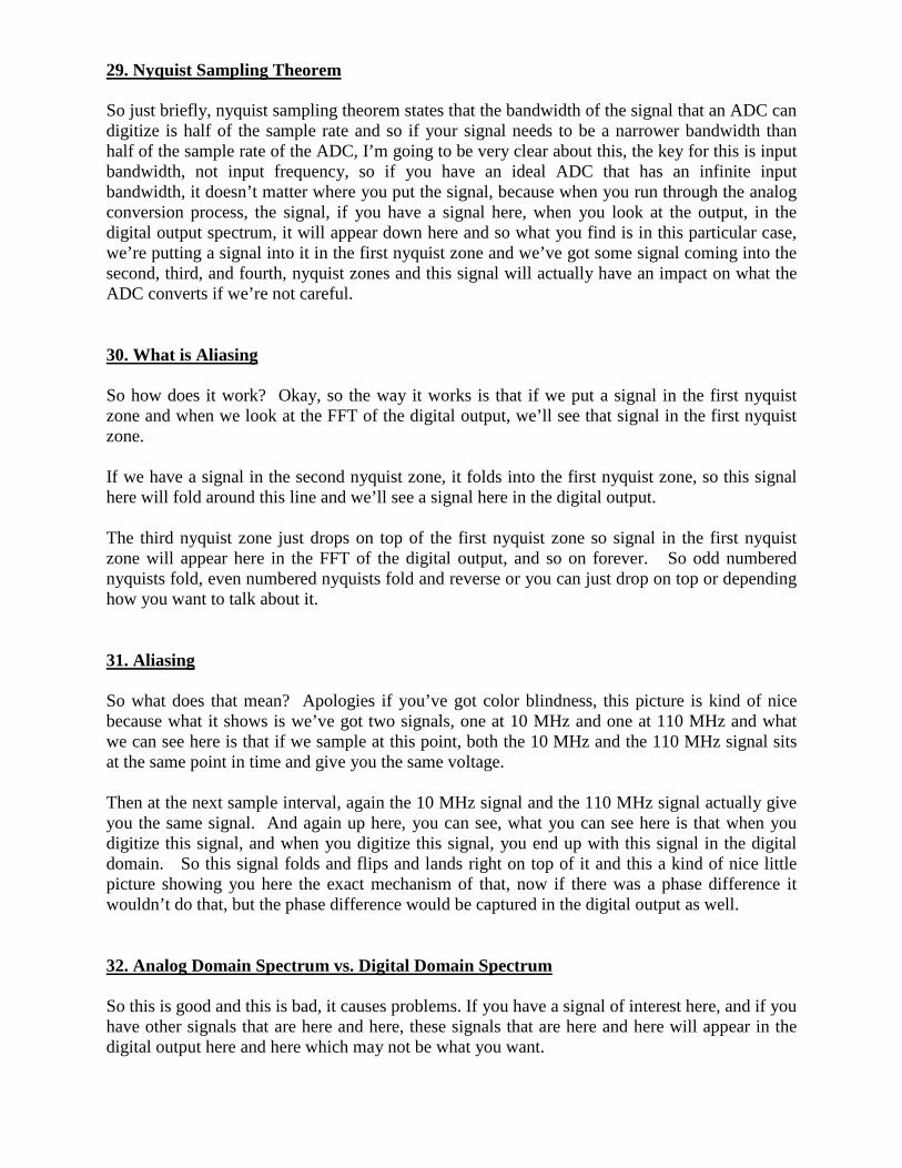
29. Nyquist Sampling Theorem So just briefly, nyquist sampling theorem states that the bandwidth of the signal that an ADC can digitize is half of the sample rate and so if your signal needs to be a narrower bandwidth than half of the sample rate of the ADC, I’m going to be very clear about this, the key for this is input bandwidth, not input frequency, so if you have an ideal ADC that has an infinite input bandwidth, it doesn’t matter where you put the signal, because when you run through the analog conversion process, the signal, if you have a signal here, when you look at the output, in the digital output spectrum, it will appear down here and so what you find is in this particular case, we’re putting a signal into it in the first nyquist zone and we’ve got some signal coming into the second, third, and fourth, nyquist zones and this signal will actually have an impact on what the ADC converts if we’re not careful. 30. What is Aliasing So how does it work? Okay, so the way it works is that if we put a signal in the first nyquist zone and when we look at the FFT of the digital output, we’ll see that signal in the first nyquist zone. If we have a signal in the second nyquist zone, it folds into the first nyquist zone, so this signal here will fold around this line and we’ll see a signal here in the digital output. The third nyquist zone just drops on top of the first nyquist zone so signal in the first nyquist zone will appear here in the FFT of the digital output, and so on forever. So odd numbered nyquists fold, even numbered nyquists fold and reverse or you can just drop on top or depending how you want to talk about it. 31. Aliasing So what does that mean? Apologies if you’ve got color blindness, this picture is kind of nice because what it shows is we’ve got two signals, one at 10 MHz and one at 110 MHz and what we can see here is that if we sample at this point, both the 10 MHz and the 110 MHz signal sits at the same point in time and give you the same voltage. Then at the next sample interval, again the 10 MHz signal and the 110 MHz signal actually give you the same signal. And again up here, you can see, what you can see here is that when you digitize this signal, and when you digitize this signal, you end up with this signal in the digital domain. So this signal folds and flips and lands right on top of it and this a kind of nice little picture showing you here the exact mechanism of that, now if there was a phase difference it wouldn’t do that, but the phase difference would be captured in the digital output as well. 32. Analog Domain Spectrum vs. Digital Domain Spectrum So this is good and this is bad, it causes problems. If you have a signal of interest here, and if you have other signals that are here and here, these signals that are here and here will appear in the digital output here and here which may not be what you want.
And one of the interesting side effects of an ADC is, in this particular example you can see that this signal here and this signal here, end up still within the bandwidth of this ADC. So it could be that you actually want to capture this signal and this signal because these three signals don’t actually overlap with each other in the final digital output. So you ca actually build a system that digitizes this and this all at once. The only thing is when you look at the digital output; you don’t know whether this signal occurred here, or whether it occurred out here. So there are applications where you can put signals in different nyquist zones simultaneously and digitize them all at once. But what’s important when you do that is that the signals don’t sit on top of each other after they have folded back down again, because if they do, then you know, they kind of mix together and unless that’s what you want, which generally it’s not. It’ll cause your system not to work properly. Generally, when we talk about this stuff, we look at this being distortion and we try to filter out, so we want to put a filter around this signal, such as the ADC doesn’t see these signals. 33. Typical Receiver System (i.e. superheterodyne) So in a typical receiver system, we might have an RF amplifier, some initial mixing system and another mixer followed by the ADC, and we insert band pass filters in the right place and if we put the right band pass filter around it, this ADC will only digitize the signal of interest and won’t do anything with these signals. So it’s important to design this filter correctly. This is what you’d call a more traditional radio where you’d have a superheterodyne, you would do two conversion steps. 34. Undersampling Receiver System In more modern radio systems you’ll do an undersampling receiver where you would only go through one mixing step and the ADC provides the final mixing function. This is a typical example where you’d actually park the signal here in the third nyquist zone and the ADC then does the down conversion. This is really good because you can eliminate a down conversion stage which is board area, power and money, and replace it with an ADC that you know in the past, was even more board area, very power and money. But these days, these ADCs, the performance that ADCs gives you is very good and you can do this. 35. Undersampling System Sampling Rate Consideration There are several things that you don’t want to do, you really don’t want to park the signal across two nyquist zone boundaries, this is about the worst place to put a signal because what happens is that this signal folds on top of this signal and you end up with a spectrum that looks like this and this is just a mix of this half and this half, and generally that’s a bad thing to do.
So if you park your signal across multiple nyquist zones, you want to make sure that you do it in such a way that the signals don’t land of top of each other. Generally you don’t do that, and you just put the signal in one place and filter the rest. 36. Undersampling System Sampling Rate Consideration Undersampling systems are a little bit nicer because it relaxes the filter requirements substantially, to get good roll off in the filter; it’s easier to build a filter for those high nyquist zones applications. But as we see later, sampling in the high nyquist zones can cause issues with the clock generation and new ADCs are more sensitive to jitter than they might be in a traditional sampling system. 37. Can All ADCs Undersample? Can all ADCs sample? Well clearly not, many precision ADCs used in signal architectures and they’ll be baseband low pass delta sigmas, if you feed signals in that are outside of the low pass function, you’ll just not get any signal coming out. Those are traditionally very severe roll off with input response. Pipeline ADCs usually have a very high performance, high bandwidth sampling network at the front of the converter and they’re usually designed to do that, so what you’ll find now is that the majority of ADCs you can buy commercially that allow you to undersample RR pipelines or maybe flash converters with lower resolutions. An example of such a data converter is this part that we designed seven or eight years ago, it’s 500MSPS with 12-bit ADC, and it’s pretty happy sampling signals at 2GHz, so that each nyquist zone is 250MHz wide, so this thing can sit with 8 nyqiuist zone signal going into it and still give you a pretty good performance. It gets worse at higher input frequencies, but you can digitize to very high input bandwidths on this type of data converters. Precision saws I guess can sample in the second nyquist zone, they’re usually limited by the time constant of the network that you’ve got. I think if you were to sit and look at the papers presented at ISSCC for the last few years, there’s been a lot of high speed saw ADCs presented that have very high bandwidth and extremely small sampling networks. Those ADCs will actually work quite well at sampling higher nyquist zone frequencies. But I think what you find if you go look at the commercially available ADCs, those types of ADCs, you can’t just buy them there, they’re usually integrated inside some SoC. So out of all the ADCs that you can go buy, the ones that can undersample, are generally pipelines.
38. Overview of Topics I’m going to talk a little bit about the analog front-ends and how you might couple into a high speed ADC, generally there’s three. Two different ways of doing this, transformer coupling which traditionally, has been the way they’ve done it. More recently you’ve been able to buy commercial amplifiers, op amps that can do this. And then we’ll talk a little bit about the benefits of a buffered ADC inputs versus an unbuffered ADC inputs and what that even means and why that matters. 39. Transformer Example Transformers have been the method of choice for connecting signals generally, radios, discrete radios, single-ended in nature, LNAs are typically a transistor with some resistors on it, and antennas single-ended and the output from that is single-ended. If you go look at a lot of highly integrated receivers, I think you’ll see a lot of differential architectures in those cases but in the majority of discrete radios, those don’t work that way. The majority of discrete RF design is not done that way, it’s done single-ended, so you have this single-ended radio domain. All the high performance ADCs you can buy, all of them, when I mean high performance I mean high speed, high resolution, 10, 12-bits and up, 200 M/samples, 100 M/samples and up, they’re differential inputs. So you have this problem of connecting this single-ended signal source into this differential ADC, and typically actual amplifier circuits have limited the performance substantially so we’ve got a transformer always on to do that. So this is like a design example here, I’ll talk a bit more details in a minute. This particular ADC has a pin called VCM, and that’s the voltage that’s needed to bias the inputs correctly in order for the ADC to function. So this is kind of handy because we can use it to drive the SM mid-point in the transformer, some transformers have sennetabs and you can drive through the sennetab and in this case we’re driving through some resistors and have a filter-cap that filters out the signal from going back into the VCM. We have some kind of network we put on the chip and these do various different things, they band limit the source, perhaps provide some filtering. In the case of an unbuffered ADC, provide some localized path to recirculate the sampling charge, and we’ll talk about that in a minute as well. You see here that we actually use two transformers back-to-back and the reason why we do that is because when you convert this single-ended signal, a differential signal, this transformer has parasitic capacitances from the windings and so there’s zero signal here, but the full signal here, and if the capacitance across this winding, here is different than the one across here, well I mean it doesn’t really matter even if it’s the same, you’re going to get more signal here just because the capacitor feedthough than you will on this side. So inherently you’re going to end up with an imbalance in these differential signals coming out due to the fact that the transformer is not ideal. So we want to try and make the signal look more differential and the way that we do that is just run it through a second transformer.
40. Transformers Transformers are good, they’re isolated, they don’t pass DC, they can be very useful in a lot of applications, can also be a problem in a lot of applications. You can use sennetabs to provide bias, you can step voltage up and down, they have turns ratios through single-ended differential, differential single-ended, do a variety of things, in fact you can even have asymmetric center taps and make different size signals if you wanted to make a transformer that way. They generally provide the best AC performance, they do have finite bandwidth, if when you get to low frequencies you need to make a transformer big, you need a big call, lots of windings to keep the inductance up. When you do that, you typically increase the parasitics and the high frequency end suffers. So you can’t have a transformer that simultaneously got very good low frequency performance and very good high frequency performance, they just don’t work that way. They don’t add noise, practically don’t add noise, the windings themselves have finite DC resistance and so therefore that is a noise source, but generally those windings are resistances are low compared to the impedances you have elsewhere in the circuit, and so they’re generally not a noise source that you need to worry about. The impedance ratio is the square of the turn’s ratio (n2Z) and the voltage ratio is the turn’s ratio, so they’re useful for transforming impedances and voltages, generally a good component. If you pick the calls too slow, and pick a too small a transformer for the size signal that you have, you will generate distortion because you start to saturate with a magnetic material in the transformer and that will cause distortion, generally you can buy transformers that don’t have those issues. 41. Transformers They have some other limitations; they have phase imbalance, and an amplitude imbalance, and flatness of bandwidth and a finite frequency bandwidth. You put a single-ended signal in, you don’t quite get a differential signal out in amplitude and phase, and that’s just due to the physical way the transformers are made. It’s very difficult to make them totally symmetrical, and even if they are totally symmetrical, you’re feeding an asymmetrical signal on one side, and expecting symmetrical signals to come out the other side, you just don’t get symmetrical signals coming out. Having said a whole lot, they’re generally way better than almost any amplifier you could put in there. 42. Transformers Here’s an example discussing how you can use two transformers, I talked about this already, to improve the balance. Another alternative is balun, balun’s are DC coupled. They’re effectively coupling inductors that work in a similar way to transformers; you can’t change the turns ratio.
For some frequency ranges, they actually give you better performance, but you’re stuck to a one-to-one impedance transformation. 43. Amplifiers Now it hasn’t really been an option to use amplifiers to do this, it’s actually kind of funny, I was just talking to Shanti here before this talk and over the last twenty years or whatever, we’ve taken ADCs down from being things that need refrigerators to cool them, to basically taking no power. The commercial high speed ADCs that we sell, often consume about a watt of power, maybe half a watt in some of the newer ones, which is huge compared to the petty ADCs that we’ve talked about in this conference, but even at a watt, it’s pretty small and you know we have a lot of customers building software to find radios that will quite happily burn 10W in the front-end before the ADC. So then you’re thinking, why did I spend such a long time designing this ADC? Because the way they get their performance out of these things, is that they take some transistor and bias the hell out of it with a lot of current and to get the linearity of the noise to be where it needs to be, and you can build amplifiers that have the performance you need with the appropriate discrete circuits. So what’s happened recently is at TI and our competitors have actually designed differential op amps. Op amps have always been these single-ended things and inside of systems-on-chips and aside of IC design where we’re quite used to designing with differential amplifiers. You can actually buy differential amplifiers now from most of the amplifier suppliers and these can have performances good enough to replace transformers in some applications and they have a lot of advantages. You can change the gain, you get power gain, you get DC couple, bandwidth, the distortion and noise, are typically the biggest limitation of using amplifiers. 44. Amplifiers and Filter Often you have to insert an Ain filter in your signal on the ADC, and the filters are lossy, so you’ve accommodate that loss somehow and transformer can’t do that, so by using some of the latest op amp ADC drivers, you could actually build circuits that have the right performance to do that. These drivers are actually interesting because they don’t necessarily have feedback resistors that are programmable by the customer. The path length out of the package, through the feedback resistor, back around to the input, it’s just too long and rough rule of thumb, a millimeter of wire is a nanohenry, so it’s pretty hard to make a resistor a package and the wiring in the connector to be much less than a millimeter, so you’re kind of limited to one or two nanohenrys of inductance in the feedback path which limits how fast a feedback system you can make at these low impedances.
So what we do when we design these amplifiers is that we put the feedback networks inside the chip so the feedback bandwidth is all localized inside the chip to very short distances and we can close the loop around the very high bandwidths. The inductances are still there, but we’re not trying to close the feedback around them, we’re just trying to drive the signal through them. So a little bit of phase shift doesn’t really hurt you as much as it does in a feedback path. So when you go look at the data sheet for this path for instance, you’ll see that it’s actually fixed gain in configurations and you can change the gain a little bit by putting external resistors in series with the inputs but generally you just go buy a different version of the part in order to get different gains. But they’re very good, these parts can produce better than 100dB distortion for signals in a 100MHz region, driving 200Ω loads and sort of in V-V peak-to-peak differential signals themselves. They’re very good and they really are an option these days for driving this type of system. 45. Amplifiers And the amp of ADC will have a worse performance than the ADCs, you go pick up your ADC and given us a thousand dollars for this, giga sample ADC we sold you, and it says that you get 67dB of SNR or whatever it says in the data sheet, and then you put in your system and then you get 52 and you’re calling up TI and you’re saying I want my thousand dollars back please, and we say no, as long as it works. Then usually what happens here is that you’ve done something wrong, and the SNR of the amp and the filter combined with some of the powers, so this actually helps you a little bit because if you get two equal noise sources you don’t double the noise, so your amplifier doesn’t need to be an order of magnitude lower noise than the data converter in order for it not to have an impact. The distortion, SFDR which we talk about all the time, they add linearly so it’s a little bit less forgiving. 46. ADC Input – buffered vs. unbuffered When you go look at high speed ADCs, they fall into two categories, the majority of them are unbuffered, most of them are made in CMOS technologies, and when I say unbuffered, if you were to sit and look at what the input network looks like, this is a typical example of what one these things looks like, is that you’ll have a sampling capacitor, a series of switches, and then some other junk. You know we have bond wire inductances, we have ESD circuits are missing here; we’ll talk about that in a second. Some network of stuff that we put inside the chip, and some more capacitors that we deliberately put inside the chip, some of these might be bond pads, this one might be a bond pad, this one’s actually deliberate. And the usual sampling process is that these switches are shut, this one’s shut and then you open this switch and that defines the sampling instinct. If everything is perfect, when you open this
switch, the charge injection in opening this switch goes evenly in both directions here and flies through this capacitor, flies through this capacitor and if you didn’t have all this junk in here, would go straight out that way in the pins, now you’ve got some inductances here, these inductances aren’t equal, you have ESD capacitors here caused by ESD diodes, so if you’ve got different voltage signals on those pins, those capacitances are different. You have connected to a transformer which is some asymmetric undetermined impedance, so there’s kind of some nasty stuff going on that has to deal with these bond wires and has to deal with the external connections, but also has to deal with the asymmetries and the capacitances that are there inside the chip caused by these relatively large ESD diodes and we can’t sell chips without ESD diodes then, well we can but generally our customers don’t like them because they bring them back to us a few years later when they’ve stopped working. So all those nonlinearities kind of add up to the fact that if you’re not very, very, very careful when you turn off that switch, you end up capturing some distortion caused by that switch turning off, and that distortion is dependent on the input signal since these capacitances change based on the input signal, so there’s a couple of things going on. One, the input is not a constant impedance because the impedance looking into here is a function of whether this switch is open or not, it’s difficult to match the input in an RF sense to the circuit. But, you know, because there’s no extra stuff there, counter repeating to noise, you end up with very good noise performance and very good distortion performance if you can drive the ADC from a sufficiently low impedance. In the lab we drive these things from 51 signal generators, pretty low impedance sources, we typically put the transformers really close to the chip, we can get really impressive performance from CMOS unbuffered ADCs. However, it’s much harder for the customer to get the data sheet performance out of an ADC that doesn’t have a buffer at its input. And in fact, actually one of the interesting things is that these architectures use bottom plate sampling, this cap, this switch is opened with the bottom plate because if you were to sample all these top capacitors, you’d get very asymmetrical performance and most of that asymmetrical performance comes around because of the PNP impedances and not well controlled. And there have been a few papers over the last few years of pretty high performance ADCs that are top sampled and the reason why they work is because there is a buffer driving a top sampling switch, and the impedance driving that top sampled switch is very stable with the input signal and the external world doesn’t have very much impact on it. 47. ADC Input – buffered vs. unbuffered So, I guess I’ve talked about this already, the effective glitch is coming back.
48. ADC Input – buffered vs. unbuffered But one thing that I didn’t talk about is why do we put all this junk in here? So we put all this stuff in here to provide a short path for the charge injection for the switch to ground, you want to keep that charge injection from the switch, local to the chip, so we’ve put these extra capacitors inside the chip in order to do that. I apologize I got a little off track here. Same thing, externally again, you put in more networks very close to the chip to absorb some of that kick back, if you connected straight into the transformer and put the termination on the primary side of the transformer, all the transformers parasitic conductances get in the way and those kick-backs have to kind of go through the transformer, you end up with wilder module transitions at the input of the ADC. So generally, you put your passive networks right at the ADC and then just run the transformer through and don’t put termination on this side of it. Higher turns ratio, higher source impedance generally gives you more trouble because you are driving from a higher impedance. Reality of the world is, you want to drive from a high impedance, so this is where you kind of run into a problem with a loss of FSDR in these unbuffered ADCs. 49. ADC Input – buffered vs. unbuffered So how do you fix this? Well you go buy a buffered input ADC. So a buffered input ADC has some sort of amplifier between the sampling hold and the outside world. If this amplifier is doing the job right, then this just a continuous frequency input impedance here, you can match it very easily to the outside world, these inductances and parasitic capacitances don’t matter too much. The source still drives the parasitic capacitance and the parasitic capacitance is nonlinear so there is a distortions turn that comes from that but that’s not really a big distortion problem, the biggest one is the kick-back from the sampling event. So buying an ADC with a buffer in it, really, really, helps. The down side is the buffer adds noise and adds some distortion while designed ones don’t really have much distortion. However, you generally have to lower the impedance of your source so much that you’ve ended up putting power outside the chip and your adding noise in doing that there. So by us doing it inside the chip, makes it a lot easier for the customer to get the performance that the ADC says it has. And what you’ll see, is that if you go look at all the really high performance 16-bit ADCs that are out there right now from TI and our competitors, you’ll see that they have buffered inputs on a lot of the very best parts that you can get. It used be that these were BiCMOS or bipolar ADCs only, because the buffers would be built-in by CMOS, recently there’s been quite a few ADCs built using CMOS and they managed to get CMOS buffers to be pretty close to the performance that you’d get out of a BiCMOS buffer. Generally they take a bit more power and not quite as linear, they’re a little bit noisier but their performance is actually very good.
This guy here is a BiCMOS and this one is a CMOS and they have buffers in them. 50. ADC and DAC Functions We’ll talk a little bit about references, we put a DAC in here, so reference is the code that comes out is the input voltage divided by the reference times two to the number of bits, if you move the reference around, the code changes. 51. Noise and ENOB of ADC So just some formulas for calculating from signal into noise distortion, and ENOB, which I just put in there, not for any good reason but they’re in there anyway. 52. Measuring Reference Input Noise So how would you measure the noise of a reference? Well one of the interesting things you can see here is that if the input signal is zero, the code comes out as zero, independent of what the reference is. If the input signal is VREF, then the code that comes out is VREF but it’s dependent on the reference now. So what you can do is depending on where you place the reference, the signal compared to the reference, you either measure the noise of the data converter or you measure the noise of the reference, plus the data converter. Different data converters do this in different ways, depending on how they define zero, some are bipolar around zero, plus and minus. Saws are typically, zero, zero, plus is plus in a single-ended input. So in the case of this power, which is a single-ended input, we feed the reference into it and then we make a very low noise source, voltage source, that we sweep to zero to full scale. 53. Noise Contribution If you look at the noise that comes out of the ADC, what you’ll see is that zero input voltage, you get 26, 27mV, and at 4V you get 40mV of noise. What’s happening here is that, at this voltage, there is no reference noise and one of the disturbing things about high precision ADCs until you’ve used them before, you plug them in, turn them on, short the inputs together and look at the output, it moves. The numbers tickle around and that’s because it’s digitizing the thermal noise that’s there in the data converter. So if you measure it here, you get, you actually measure in the internal noise of the ADC, if you measure it here, you’re measuring in the reference on the internal noise. So by comparing this measurement to this measurement, you can actually separate out the reference noise from the internal noise of the ADC. So this is a good way of checking whether your reference is giving
you problems or not. If your reference is designed realty well, you wouldn’t see an increase in this at all. Piplelines typically, this would actually look like, would actually be a signal with either side, with zero in the middle. With pipeline ADCs, if your signal’s got a very high peak-to-average ratio, the reference generally doesn’t impact the noise very much because most of the time, the reference signal is small compared to the reference, and so the additive noise from the reference is small, if the signal is big, you get more noise, but if your peak-to-average ratio is big, then the way that generates its SNR is not so bad. 54. Quantization of Reference Noise So here’s an example here where we put in 0 and we get 27µV of noise, we put 4V, we get 43µV of noise and you can run through the math and separate out those two noise sources. 55. Sources of the Noise in REF50xx So typically you’d go buy a reference chip, in this case, there’s a family of parts called the REF50xx, inside here you have an amplifier with some gain, you have some reference which in this case is a bandgap reference. And you basically have two noise sources, one is the bandgap and one is the op amp, and the resistors and this bunch of noise sources actually, but split it into two, this amplifier and the bandgap. 56. Low Pass Filter Shapes the Output Noise Spectrum There are several different types of noise that effect you in this low frequency domain, you 1/f noise, at very low frequencies you have noise sources like random telegraph noise that look like discrete steps in voltage that occur at the hertz level. At the high frequencies, you have white noise and white noise comes from just thermal noise and resistors plus short noise and transistors. And then the noise itself has some kind of bandwidth, it’s not infinite in bandwidth because the circuit is usually not infinite in bandwidth so the noise will roll off at some frequency response. 57. REF50xx Noise Test Circuit So, you want to test the noise of one of these references. You know you could stick a capacitor on the output of it which helps filter the noise and you’ll go measure the thing. 58. Capacitor Equivalent Circuit The capacitor is not ideal, a capacitor has some equivalent inductance, it has some leakage resistance, it has a series resistor and the capacitor itself. And this is actually kind of counter intuitive as to how it might necessarily manifest itself as integrated noise in the final system.
59. Capacitive Load with ESR The ESR gives you a zero, this capacitor gives you a pole based on the output impedance of the amplifier in the reference circuit. 60. Measured Noise for different BW and LP Filters This is a kind of interesting table because you think, okay, I can make the capacitor bigger and make the capacitor have no series resistance so these ceramic capacitors have practically no series resistance, the tamlin capacitor actually has a relatively high series resistance, I think this is a tamlin as well. But you see here that actually this guy gives you better noise than the ceramic and the reason why that’s the case is that the ESR being a little bit even though that ESR itself is a noise source, it helps stabilize the amplifier a little bit. And so because noise is integrated in the square root of bandwidth, if you have a lot of peaking going on in the high bandwidth section, you’d get a lot of noise. So stability can actually cause you bigger noise problems than just making the capacitor bigger, it doesn’t necessarily make it better, I guess is what I’m getting at. Ceramic capacitors when they first came out, we thought, well, these were great, we could put down 2 µF capacitors and they’re tiny and they have very low series resistance. What you find with these very dense ceramic capacitors that you buy, is that they have a very big tolerance, they’re usually +20, - 80% tolerance and they have a brutal temperature coefficient, so in cases when you need very low ESR, they’re good, but in some cases, you’re better off with just a tamlin capacitor, now tamlins can have problems as well mind you because depending on how they’re manufactured, usually they’re specified at a maximum ESR. 61. Capacitor Equivalent Circuit Just to recap the ESR is this series resistor, in series with a capacitor. 62. Measured Noise for different BW and LP Filters So tamlins usually spec a maximum ESR when you buy one, they very rarely spec a minimum ESR, and actually sometimes they can be zero or practically zero which is a bit of a problem because you might have a capacitor for instance, that’s this guy here, might have a maximum ESR of 2Ω, and a minimum of ESR that’s 0. And that’s actually very difficult to deal with because that’s moving a zero around a lot in a frequency response. So you have to be a little bit careful sometimes and in some cases, you might be safer adding a very small fibrator resistor in series capacitor because if that cap has an ESR that goes from 0 to
2Ω, and you insert ½Ω in series with it, now your impedance goes from ½Ω to 2 and a ½Ω which is kind of a controlled range, whereas from 0 to 2Ω is an uncontrolled range. So there might be situations where to get better performance over manufacturing, you actually deliberately insert resistor in series with components. 63. Filtering Internal Bandgap Reference Another thing you can do here is that these pins, these chips usually have a trim pin that allows you to tweak the absolute voltage of the reference of the tamlin a little bit, but they also allow you to filter the internal bandgap before it hits the op amp. So you can put a capacitor on these pins which help further reduce the noise. 64. Measured Noise with Added Bandgap Filters And there’s a table here showing how you can get lower noise and you can see adding a microfiber to the trim pin takes the noise down by a factor of 2.5. 65. REF5040 Output with 10µF and 10mΩ ESR Capacitor And this is an example of a ceramic capacitor that is causing the aleph to go a little unstable, you can see the is peak in the response here, this is actually generating a lot of noise because of the fact that you’re peaking a little bit, putting a little bit more resistance in series with the output of this capacitor, series of this capacitor will actually bring the noise down, so that’s just something to watch for. 66. Added RC filter on the Output Then you can add yet more filtering if you want to band limit it further, and here this will actually reduce the noise substantially, 67. REF5040 Output with added RC Filter And you see here, we’re down to 2.2µV by adding in this network which is nice. 68. Added RC filter on the Output A few things you need to watch for. This 10µF capacitor, if it has any leakage, that will actually make this reference, less of a reference, it will move, 10µF capacitor quite often have leakage and that leakage is strong function of temperature usually, and strong function of time so you have to be careful when you insert impedances in series with voltage references because they become susceptible to DC leakages.
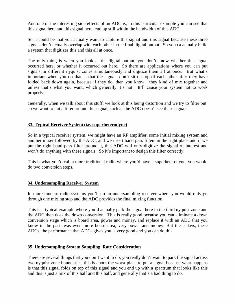
69. SAR ADC Capacitive Conversion Network So this is an example of what’s inside of an SAR ADC. Typically we have an array of capacitors that is successfully connected to the reference in different orders in order to do the actual conversion. 70. REF Input With Proper Buffer What we see and what you did here, was we exaggerated the reference by adding a series resistor. You can see that it’s similar to what we saw on the analog inputs. You can see these spikes on the reference as it goes through the conversion process and as you end up at the end of the conversion process, this spike gets smaller, and smaller, and smaller. These need to be controlled such that the reference settles within the digital clock time period. 71. REF Input With Wrong Buffer And this is an example here where you got the wrong capacitor, wrong filter network. 72. Voltage-reference circuit with added buffer and output filter So what you end up doing, okay, so you made this beautiful super low noise reference and you stick an op amp in series with it, and the op amp there, provides a low impedance to drive the reference pin of the ADC and then this guy can go through a very similar design process as to what we talked about on the input. The op amp here will add noise but this is a very low noise op amp. One thing to watch out for is this op amp has an input bias current and the input bias current causes a DC voltage across this resistor, that input bias current is a function of temperature and that in turn will cause a temperature dependent drift in the voltage reference. So effectively in analog everything on a board will bite you in one way or another so you fix one problem, you create another but buying the right components, you can usually get around that. 73. Clock Jitter Impact to Data Converters Okay, let’s talk a little bit about clocks. So, and you’ll see pretty quickly, this is a function and this is something you worry about in high speed ADC, so clock jitter is the fact that clocks are not perfect, the actual position of a clock, varies to what you would like it to be in time, and that’s what we call jitter. And what you can see here is that if this clock edge moved back and forth a little bit, the voltage you sample moves up and down a little bit, and that causes an error in the conversion. Now, if
this is a random source, it ends up looking like noise, if somehow the clocks got a signal dependent nature to it, then that looks like distortion. In fact, actually, I coauthored a paper here a couple of years ago when we deliberately jittered the clock with the signal in order to cancel out a distortion source, so sometimes we would actually do that deliberately to correct for something that is going on inside the ADC. What you can see here is that the SNR due to jitter is the function of the jitter and the input frequency. So if the input frequency is low, this is a negligible distortion source, noise source, if the input frequency is high, this is a significant source. 74. Jitter Impact with respect to Frequency And this is pretty easy to see because you’ve got some slow sine wave when you’re a sampling it, up on the easy bit at the flat bit at the top, jittery signal only changes the voltage by a little bit. If you’ve got a faster signal, it’s got a high slew rate when you’re sampling it, on this edge here, you can see that jitter in the clock changes the voltage by a lot. 75. SNR due to jitter vs. Analog Input Frequency So you can make a table here, I’ve got another one here just plotting this, just showing it. For theoretical jitter, the limited SNRs, you need progressively lower and lower clock jitter in order to achieve the SNR that you would like to get. 76. Total Data Converter SNR Performance In a high speed ADC data sheet, you’ll see a couple of things; you’ll see aperture jitter is what we spec because we can’t spec clock jitter, because that comes from the outside. We can tell you what you need to do in order to get the performance but we can’t spec clock jitter, so we talk about aperture jitter, and this is extra jitter that our chip adds on to the jitter of the clock source that you provide to the ADC. On a 16-bit 200 mega sample class ADC, this aperture jitter is in a region to 10 to 30 femtoseconds, it’s really, really low and you need this guy to be about the same in order to keep the total jitter of these two combined under maybe 50 femtoseconds in order to 16-bit performance at high IFs. The good thing is that jitter adds to some of the squares so that helps you a little bit, and you have a variety of noise sources you worry about in ADC design, quantization noise is just a function of the digital size of the LSB. High performance ADCs generally have more bits than their SNR leads them to believe, so you’ll see a 16-bit ADC might have 77dB SNR, that’s not very good, a 16-bit ADC should have maybe 6dB SNR.
The reason why we do that is because adding extra bits to the ADCs is cheap in terms of power and die size and reducing thermal noise is expensive in terms of power. So when you want to add your noise source, your actual SNR is some of all this stuff, you don’t want this to be a player in the noise equation, you absolutely don’t want it anywhere near the final noise results. So as a consequence what you’ll see is in the high speed world, what we call 14-bit in a 16-bit ADC, is significantly lower SNR than you might call a 14-bit or a 16-bit ADC in the low speed world, and that’s just purely a power thing. We could add a couple of bits for almost no power, but if were degrading the noise of a converter by placing it by quantization noise, than generally we’re wasting power. By deliberately jittering the clock and doing a variety of other things, you can actually separate out these different noise sources in the measurement as well. 77. Band Limit Clock Phase Noise So how do you actually get the performance? So the clock tree is generally very high bandwidth, we try to get very high performance so what we need to do in order to prevent the noise from the clock source feeding into the data converter, we want to band limit the clock, so we run the clock through a bandwidth filter in our bench setups, we have these big boxes with filters inside them, and then we have these expensive signal generators and we have discrete crystal filters at different frequencies and automated mains of switching between these filters in order to do frequency conversion rate sweeps on our characterization set ups, it’s very time consuming job to do manually because effectively you have to put a filter in skew with the clock source on every clock frequency you want to measure the converter at. For the very best in performance we buy these surface filters and they have very, very narrow bandwidths of only a few kHz, and you can take a relatively noisy clock source and feed them through these crystal filters and end up with very good performance. 78. Example Clock Circuitry And one of the easy ways to do this is to make good clocking source is to buy a clock chip. This is a part that we make, the other parts are from our competitors, they’re interfaced directly to a VCO. Inside of these chips, some of them have jitter cleaners which are just PLLs that limit the bandwidth of the noise that comes through from the clock. Then you take that, they have low impedance driver circuits, you feed that into a crystal filter, it’s relatively easy to go get a clock source that has jitter of the order of 10s of femtoseconds by doing this. In fact, you could quite easily with a system like this, make noise that’s as good as an 8644, any 8644 is not good enough to measure most of these high performance ADCs, usually we have to filter it subsequently.
I don’t know if any of you have ever tried moving an 8644. You know a lot of test equipment is what I call mostly empty. You know, you take the lid off it and its air inside it and you pick them up and it used to be the CRT will be the heavy bit and oscilloscopes were basically designed around the CRT. These days the little crystal panels make them a bit smaller, but they’re pretty light piece of equipment. These are signal generators that are full of stuff, I mean really, really full. I mean this is a bench top signal source that has a two man lift requirement; it’s a big heavy piece of equipment. And so I spend quite a lot of time building these application diagrams telling our customers how to achieve that type of a performance on something that you could just put on a board. Of course the difference here, is that big heavy piece of equipment, can change the frequency and you can measure it in different places. Here is just one of the frequencies, but most applications just have one frequency so that’s okay. 79. Power Supply Let’s talk a little bit about power supplies. Most ADCs have separate supplies for the analog and digital, generally you want to keep the analog supply clean; you’ve got to watch out for what the power supply rejection for the ADC might be. One of the things that you’ll see when looking at ADCs is that we’ll have a plethora of power supplies sometimes different voltages. And the reason why we do that is because it makes it easier for us to get lower power numbers so we only run bits of the circuitry on the lowest supply possible. However this is kind of problematic for customers because they generally don’t have all these power supplies available to them so they have to go and regulate down from some master supply. Traditionally that’s being done with LDOs but then you don’t really get any power saving if you do that. Increasingly these days you see people using DC-DC converters to help improve the power efficiency. 80. Traditional ADC Power Supply So traditionally you might have an LDO that just takes you to 5V and then drops it down to whatever the thing needs. All the voltage drop is just dropped dissipatedly through a switch somewhere, through a transistor somewhere. More modern approach might be to use some sort of switching regulator to drop down to some intermediate voltage and then through and LDO to get down to a low voltage. This is a much more efficient approach but can generate some problems itself.
81. Typical LDO power supply It’s possible you can get away without separate supplies of the analog to digital just by separating the analog and digital with ferrite beads so you might come out at LDO run through two ferrite beads which are basically lossy inductors and filter them separately and in some case that might work. It might be good enough for you. 82. Example LDO power supply – ADS2P49 Other cases for EVM for this particular part we found that we could actually just via down and via up through the PC board and that was enough inductance between the supplies if they were done correctly and the layout was done right, then we could get the performance we needed without actually adding any ferrites into it and these inductors were just basically in the PC board itself. 83. Example LDO power supply – ADS2P49 So there’s an example here doing that. We got the spurs down on our EVM low enough for this particular ADC to clean it up but you can still see power supply spurs coming through. 84. RC Snubber Circuit Switching power supplies are good, they’re generally operated in discontinuous mode in these low current applications, what that means is that the inductor current drops to zero at some point in the conversion cycle. When the inductor current drops to zero, you usually get this ringing response on the switch node, and this ringing response is a function of the inductance whenever the parasitic capacitance sits on that node. The best efficiency is usually to let it ring, but that ringing could be some RF frequency which your ADC could capture and subsequently convert. If that’s a constant thing, it’s not such a big deal, but generally it’s not because it’s a function of the load, so you want to snub that out so what you can do is you can put a small RC network on the switch node and at the expense of a little bit of efficiency, you can snub the ringing out entirely or pretty much snub the ringing out and this may make a substantial reduction in the power supply related to the noise that you get out of switching power supply. So if you’ve got switching power supplies, probe around on the go look for ringing and you may find putting in a little snubbing network. Quite often with these analog systems you kind of put your hand around the board and touch things until it gets better and then go figure out why touching that place made a difference.
Debugging high speed RCs is really challenging because the signals are effectively settling to microvolts and doing nanoseconds, there’s not much you can do. One of the most powerful debugger techniques we ever came up with was taking tiny little pieces of copper tape and putting them on top of the chip and pushing them around with a probe until we found where they made a difference and then going and looking at the circuit underneath and seeing how adding parasitic capacitance there would actually fix things, we debugged pretty much all of the high speed ADCs using that approach. That’s the secret thing I’ve told you today so hopefully you don’t remember it. 85. Conclusion I’m going to wrap up here. You know I had a hard time coming up with conclusions here because the talk was kind of touching a lot different things. And the other thing I was asked to do is put in references, well it’s difficult to reference stuff because it’s kind of generic basic information that you can derive custom from data sheets, websites, so I’ve referenced Aristotle here, the more you know, the more you don’t know. So I think it’s clear here, we’re just scratching the surface of what could be going on inside an analog high performance system. 86. Wrap-Up You got to be very careful in how you design stuff that goes around these things. The analog input signal is generally the place you need to give the most attention to. It’s where you lose the performance the fastest. Clocking, clocking is solvable, I mean it’s a very solvable issue but don’t be surprised if you burn quite a bit of power in building a clock source. It needs to be budgeted up front and if you’re thinking of dropping some IF stage in your radio because you’re going to save a watt, just make sure that you’re not adding a watt back in your clock source to get that. Now it could be if you have many ADCs, that adding in the clock thing can be distributed across a few ADCs, and you can save power, but just a single ADC, you may be just better off just leaving the conversion stage in there and buying a cheaper ADC, although we want you to buy the expensive ADCs because that’s where we make the most profit. Power supplies are usually really ugly, whenever you’ve got op amps or class AB amplifiers, processing signals, the power supply current waveform, generally looks like a rectified version of the signal plus some dc level. That is usually the biggest distortion generator in your circuit, period. Majority of op amps that you might buy have class AB output stages and this why discrete amplifiers are often good because they’re more continuous current, their supply current waveforms are in a class A amplifier of the signal. And the signal when added to itself, usually just generates a gain error. In a class AB amplifier, or a differential class AB amplifier as well, the power supply current is a rectified version of the signal. If you add that into the signal somehow, you get all sorts of ugly stuff.
So the power supplies are the biggest distortion source in any amplifier based system, is in the power supply, if you really keep it separate enough, it’s okay, but if it leaks into the signal somehow, you really get messed up. The digital signals are a whole slew of other things to talk about, in a giga sample ADC, you have maybe 12-bits of signal, talking away of 2GHz samples, we generally multiple data rate these signals these days so we might have core data rate outputs where you have 16-bit ADC multiplexed over 4 serial lines, you’ll see that the various manufacturers do different things to scramble the data, to try to remove signal dependence from the digital data word so you get less issues with the signals, in the digital signal interfering with the analog. One of the things that is kind of nice in a lot of ADCs you buy now, they have LVDS outputs which are relatively quiet. They’re usually designed to drive signals over 5-6 inches of PC board. If your digital circuit, your FPGAs is right next to the ADC, you don’t need such a hefty LDS signal and most of these ADCs can figure them out VDS signals to have smaller swings which usually still work quite effectively over short distances but significantly reduce the amount of noise radiated by the digital interface. So there’s a lot of stuff to talk about digital signals that I haven’t covered in this talk Further reading Further reading, web is the best place to find out information on these things these days, our website is extensive and has numerous selection guides and data sheets and applications notes for amplifiers and ADCs. Our competitor’s websites are good as well. One book that I really like and you can actually buy this as a book, where they have the PDF on Keithley’s website, is this low measurements handbook from Keithley. It talks about all sorts of bizarre, phenomena, that goes on inside measuring small signals and this is an excellent read for anybody who is interested in furthering their knowledge in precision low level measurements, in fact the book is nice to have, it’s a little orange book they might change the color with each addition, but you can actually just download the whole thing off the internet. I didn’t ask Keithley permission but I figured if they’re giving it away free on the internet, they’re not too fussed about me telling you about it. Okay, so that’s it, I’m open to some questions.