isscc 09 plenary bohr presentation
TRANSCRIPT
1
The New Era of Scaling
in an SoC World
Mark Bohr
Intel Senior Fellow
Logic Technology Development
2009 ISSCC

2
The End of Scaling is Near?
“Optical lithography will reach its limits in the range of 0.75-0.50 microns”
“Minimum geometries will saturate in the range of 0.3 to 0.5 microns”
“X-ray lithography will be needed below 1 micron”
“Minimum gate oxide thickness is limited to ~2 nm”
“Copper interconnects will never work”
“Scaling will end in ~10 years”
Perceived barriers are meant to be
surmounted, circumvented or tunneled through

3
Outline
• Transistor Scaling
• Microprocessor Evolution
• Vision of the Future

4
0.01
0.1
1
10
1970 1980 1990 2000 2010 2020
Mic
ron
s
CPU Transistor Count2x every 2 years
103
105
109
107
Scaling Trends
Transistor dimensions scale to improve performance,
reduce power and reduce cost per transistor

5
0.01
0.1
1
10
1970 1980 1990 2000 2010 2020
Mic
ron
s
45nm
65nm
32nmFeature Size0.7x every 2 years
CPU Transistor Count2x every 2 years
103
105
109
107
Scaling Trends
Transistor dimensions scale to improve performance,
reduce power and reduce cost per transistor

6
MOSFET Scaling
R. Dennard, IEEE JSSC, 1974
Device or Circuit Parameter Scaling Factor
Device dimension tox, L, W 1/κ
Doping concentration Na κ
Voltage V 1/κ
Current I 1/κ
Capacitance εA/t 1/κ
Delay time/circuit VC/I 1/κ
Power dissipation/circuit VI 1/κ2
Power density VI/A 1
Classical MOSFET scaling was first described in 1974
7
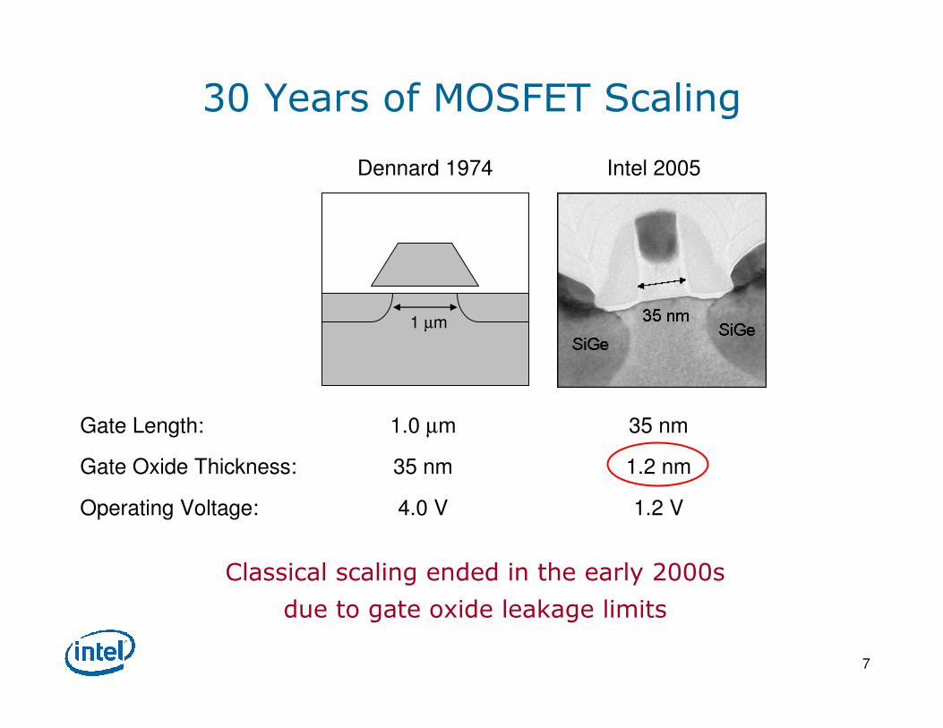
30 Years of MOSFET Scaling
Gate Length: 1.0 µm 35 nm
Gate Oxide Thickness: 35 nm 1.2 nm
Operating Voltage: 4.0 V 1.2 V
1 µm
Dennard 1974 Intel 2005
Classical scaling ended in the early 2000s
due to gate oxide leakage limits

8
90 nm Strained Silicon Transistors
High
Stress
Film
NMOS
SiGe SiGe
PMOS
SiN cap layer SiGe source-drain
Tensile channel strain Compressive channel strain
Strained silicon provided increased drive currents,
making up for lack of gate oxide scaling
9
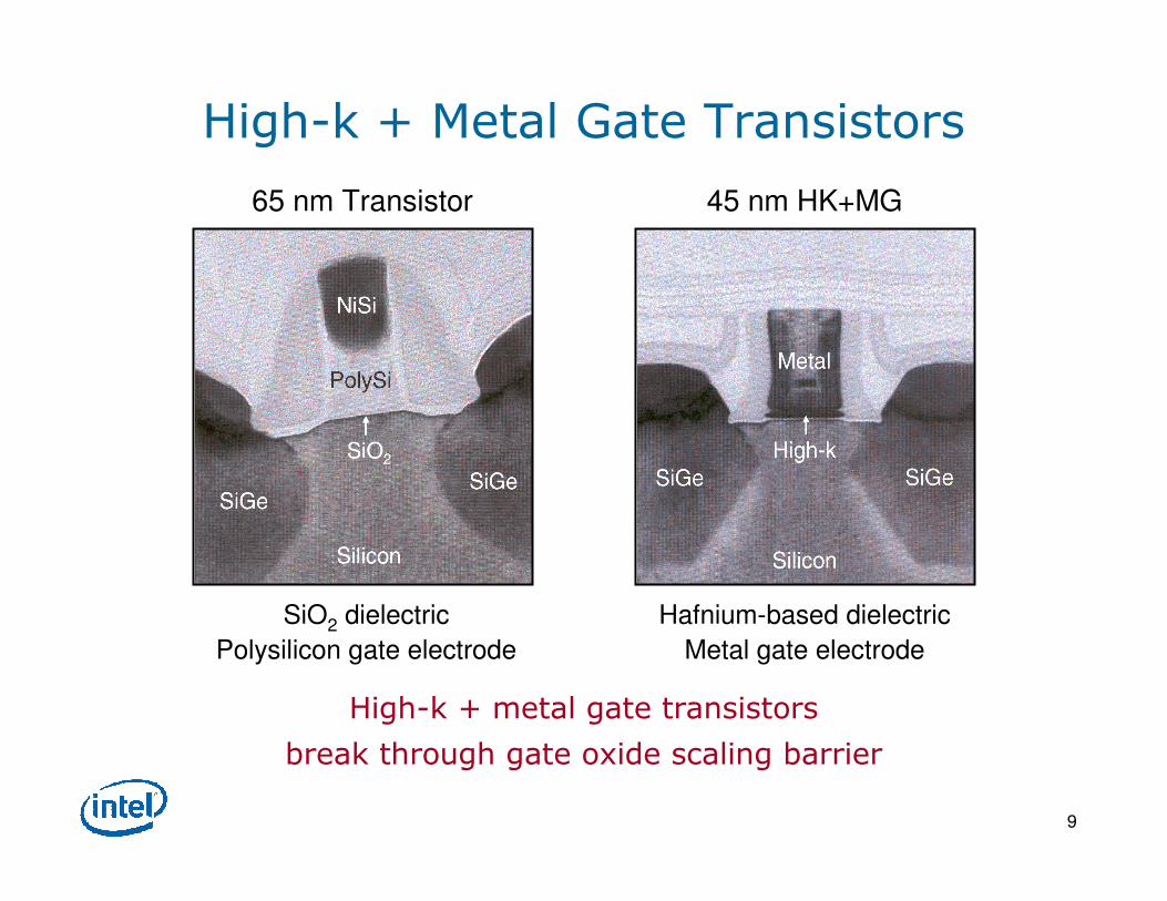
High-k + Metal Gate Transistors
65 nm Transistor 45 nm HK+MG
High-k + metal gate transistors
break through gate oxide scaling barrier
SiO2 dielectric Hafnium-based dielectric
Polysilicon gate electrode Metal gate electrode

10
1
10
100
1000
0.4 0.6 0.8 1.0 1.2 1.4 1.6
ION (mA/um)
I OF
F (n
A/u
m)
1.0 V65nm 45nm
1
10
100
1000
0.6 0.8 1.0 1.2 1.4 1.6 1.8
ION (mA/um)
I OF
F (n
A/u
m)
1.0 V65nm 45nm
+12% +50%
NMOS PMOS
100x
5x
Transistor Performance Increase
45 nm HK+MG provides average 30% drive current
increase or >5x IOFF leakage reduction
Ref. K. Mistry, IEDM ’07
11
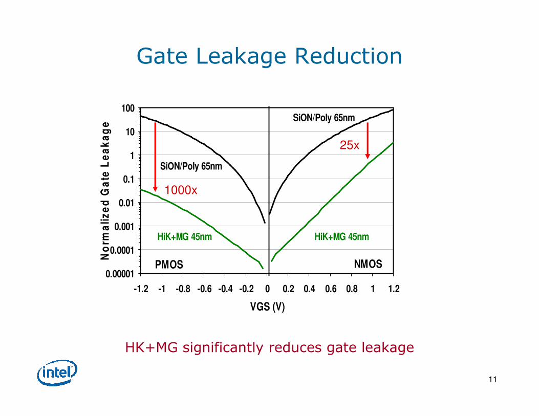
Gate Leakage Reduction
HK+MG significantly reduces gate leakage
0.00001
0.0001
0.001
0.01
0.1
1
10
100
-1.2 -1 -0.8 -0.6 -0.4 -0.2 0 0.2 0.4 0.6 0.8 1 1.2
VGS (V)
No
rma
liz
ed
Ga
te L
ea
ka
geSiON/Poly 65nm
HiK+MG 45nm
NMOS PMOS
HiK+MG 45nm
SiON/Poly 65nm
25x
1000x

12
0
2
4
6
8
10
12
65nm 45nm
Norm
aliz
ed C
ell
Leakage
IGATE
IOFF
IJUNCT
1.0V 25C
10x
Bitcell Leakage Reduction
SRAM bitcell leakage reduced ~10x

13
0.4
0.5
0.6
0.7
0.8
0.9
1
1.1
180nm 130nm 90nm 65nm 45nm
Minimal oxide scale HiK+MG
Tox scaling
VT Variability Reduction
(2
1
2
42
44 3
⋅=
⋅⋅⋅
=
ZeffLeff
c
ZeffLeff
NTqV
ox
oxBsi
Tranε
φεσ
HK+MG provides oxide scaling needed for variability reduction
Ref. K. Kuhn, IEDM ’07
C2
Normalized
to 180nm
C2
Less VT
variation

14
0.1
1
10
500 350 250 180 130 90 65 45 32
Technology Generation (nm)
M2 Pitch
(um)
0
2
4
6
8
10
# Metal
Layers
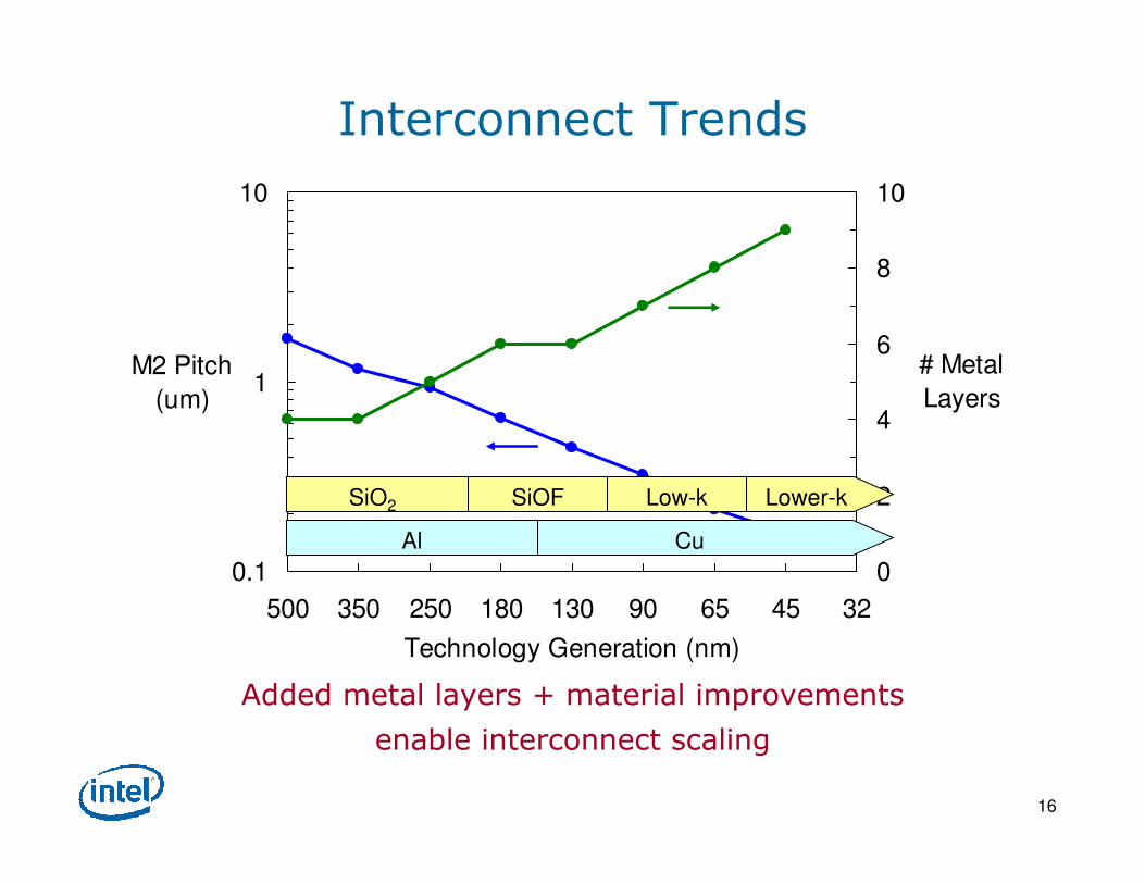
Interconnect Trends
Added metal layers + material improvements
enable interconnect scaling
0.7x per
generation

15
0.1
1
10
500 350 250 180 130 90 65 45 32
Technology Generation (nm)
M2 Pitch
(um)
0
2
4
6
8
10
# Metal
Layers
Interconnect Trends
Added metal layers + material improvements
enable interconnect scaling
0.7x per
generation
16
0.1
1
10
500 350 250 180 130 90 65 45 32
Technology Generation (nm)
M2 Pitch
(um)
0
2
4
6
8
10
# Metal
Layers
Interconnect Trends
Added metal layers + material improvements
enable interconnect scaling
Al Cu
Lower-kSiO2 SiOF Low-k
17
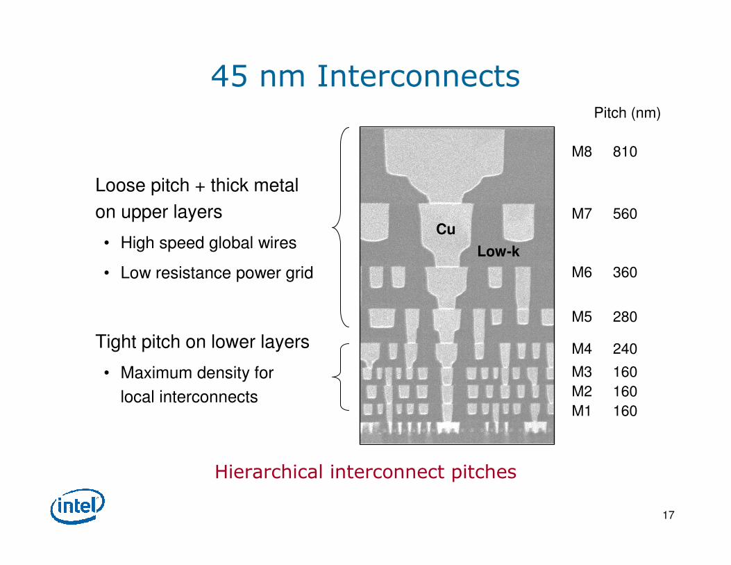
45 nm Interconnects
M8 810
M7 560
M6 360
M5 280
M4 240
M3 160
M2 160
M1 160
Low-k
Cu
Loose pitch + thick metal
on upper layers
• High speed global wires
• Low resistance power grid
Tight pitch on lower layers
• Maximum density for
local interconnects
Hierarchical interconnect pitches
Pitch (nm)
18
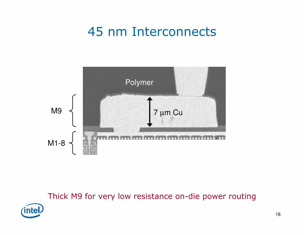
45 nm Interconnects
M9 7 µm Cu
Polymer
M1-8
Thick M9 for very low resistance on-die power routing
19
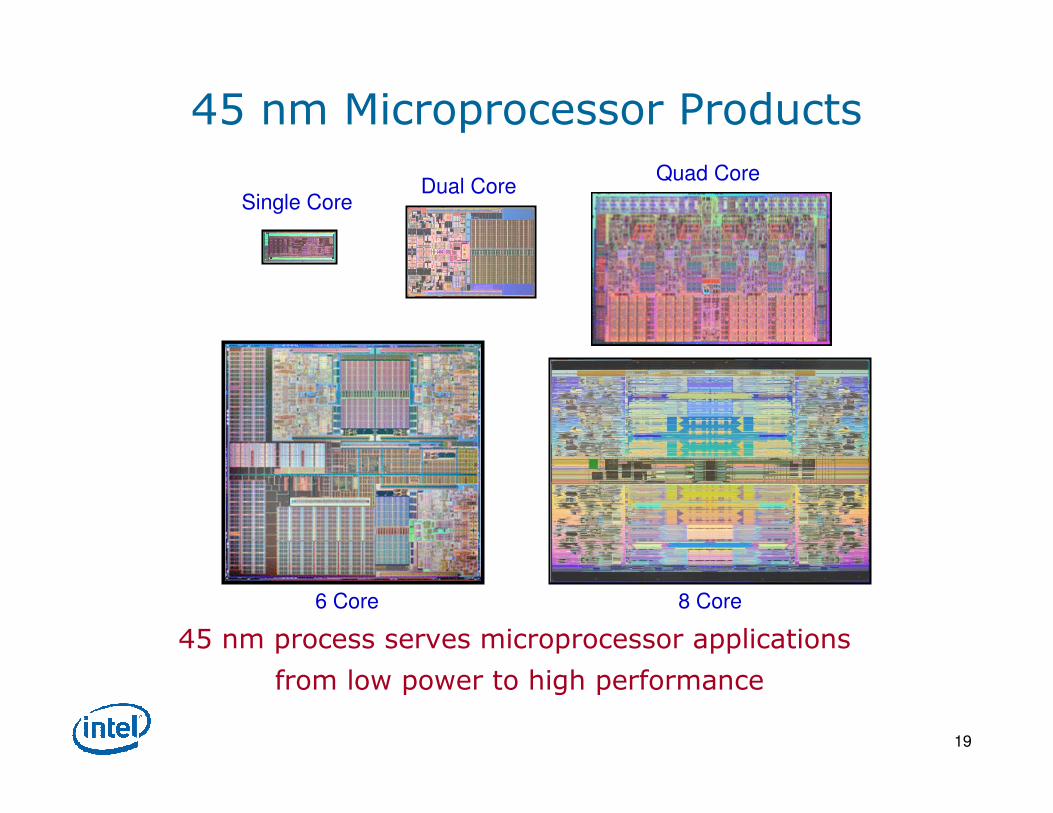
45 nm Microprocessor Products
45 nm process serves microprocessor applications
from low power to high performance
Single Core
6 Core
Dual Core
8 Core
Quad Core
20
0.01
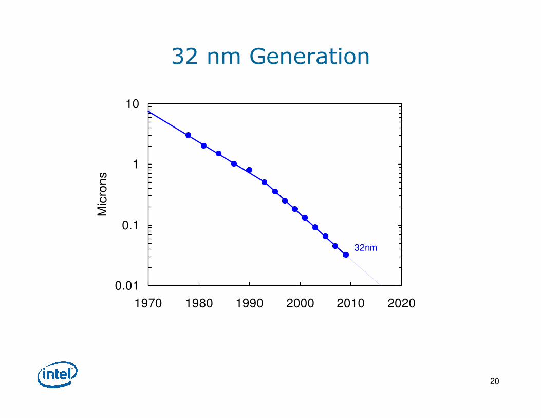
0.1
1
10
1970 1980 1990 2000 2010 2020
Mic
ron
s
32nm
32 nm Generation
21
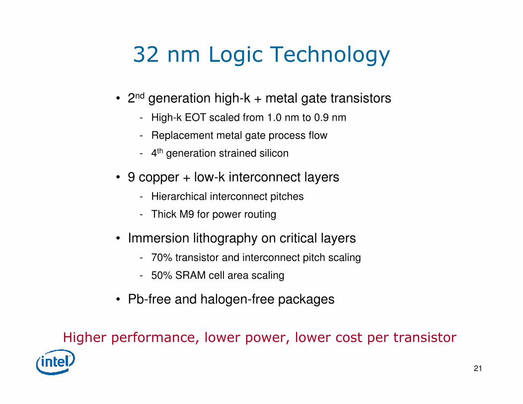
32 nm Logic Technology
• 2nd generation high-k + metal gate transistors
- High-k EOT scaled from 1.0 nm to 0.9 nm
- Replacement metal gate process flow
- 4th generation strained silicon
• 9 copper + low-k interconnect layers
- Hierarchical interconnect pitches
- Thick M9 for power routing
• Immersion lithography on critical layers
- 70% transistor and interconnect pitch scaling
- 50% SRAM cell area scaling
• Pb-free and halogen-free packages
Higher performance, lower power, lower cost per transistor

22
100
1000
1995 2000 2005 2010
Gate Pitch
(nm)
0.7x every
2 years
PitchPitchPitch
Contacted Gate Pitch Trend
Transistor gate pitch continues to scale 0.7x every 2 years
32 nm Generation
112.5 nm Pitch

23
0.0
0.5
1.0
1.5
2.0
1001000Gate Pitch (nm)
Drive
Current
(mA/um)
0.0
0.5
1.0
1.5
2.01.0 V, 100 nA IOFF
45nm
32nm
65nm
90nm
NMOS
PMOS
130nm
Transistor Performance
Drive currents continue to increase while gate pitch scales

24
32 nm Interconnects
Hierarchical interconnect pitches
M9
M8 566.5
M7 450.1
M6 337.6
M5 225.0
M4 168.8
M3 112.5
M2 112.5
M1 112.5
8 um Cu
Pitch (nm)
25
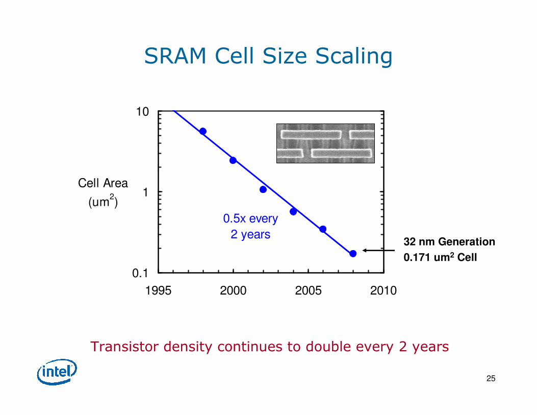
0.1
1
10
1995 2000 2005 2010
Cell Area
(um2)
0.5x every
2 years
SRAM Cell Size Scaling
Transistor density continues to double every 2 years
32 nm Generation
0.171 um2 Cell

26
SRAM Cell Scaling
65 nm
0.570 µm2
45 nm
0.346 µm2
32 nm
0.171 µm2
Good pattern resolution while scaling feature size
and continuing with 193 nm exposure wavelength
27
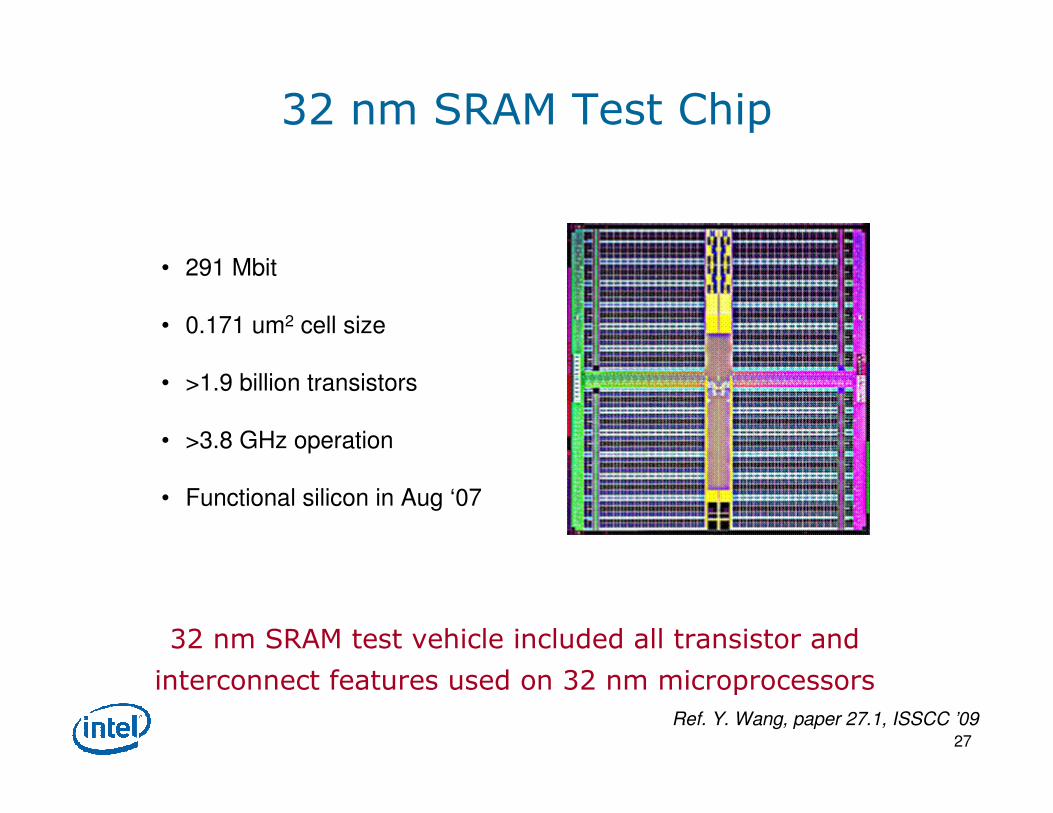
32 nm SRAM Test Chip
• 291 Mbit
• 0.171 um2 cell size
• >1.9 billion transistors
• >3.8 GHz operation
• Functional silicon in Aug ‘07
32 nm SRAM test vehicle included all transistor and
interconnect features used on 32 nm microprocessors
Ref. Y. Wang, paper 27.1, ISSCC ’09

28
30 Years of Scaling
Contact
1978
Ten 32nm SRAM Cells
2008
1 µm
29
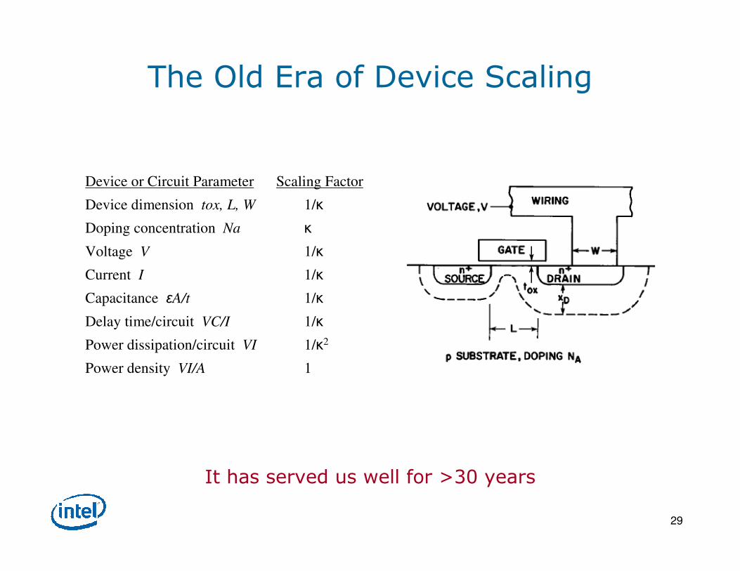
The Old Era of Device Scaling
It has served us well for >30 years
Device or Circuit Parameter Scaling Factor
Device dimension tox, L, W 1/κ
Doping concentration Na κ
Voltage V 1/κ
Current I 1/κ
Capacitance εA/t 1/κ
Delay time/circuit VC/I 1/κ
Power dissipation/circuit VI 1/κ2
Power density VI/A 1

30
The New Era of Device Scaling
Modern CMOS scaling is as much about
material and structure innovation as dimensional scaling
SiGe SiGe
Copper + Low-k Strained Silicon High-k + Metal Gate

31
Outline
• Transistor Scaling
• Microprocessor Evolution
• Vision of the Future

32
Microprocessor Evolution
More transistors
Higher frequency
More data bits per cycle
Instruction parallelism
Out-of-order issue
Multi-threading
Many of these innovations have been for improved performance,
now the challenge is to innovate for power efficiency
33
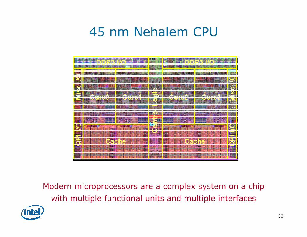
45 nm Nehalem CPU
Modern microprocessors are a complex system on a chip
with multiple functional units and multiple interfaces
34
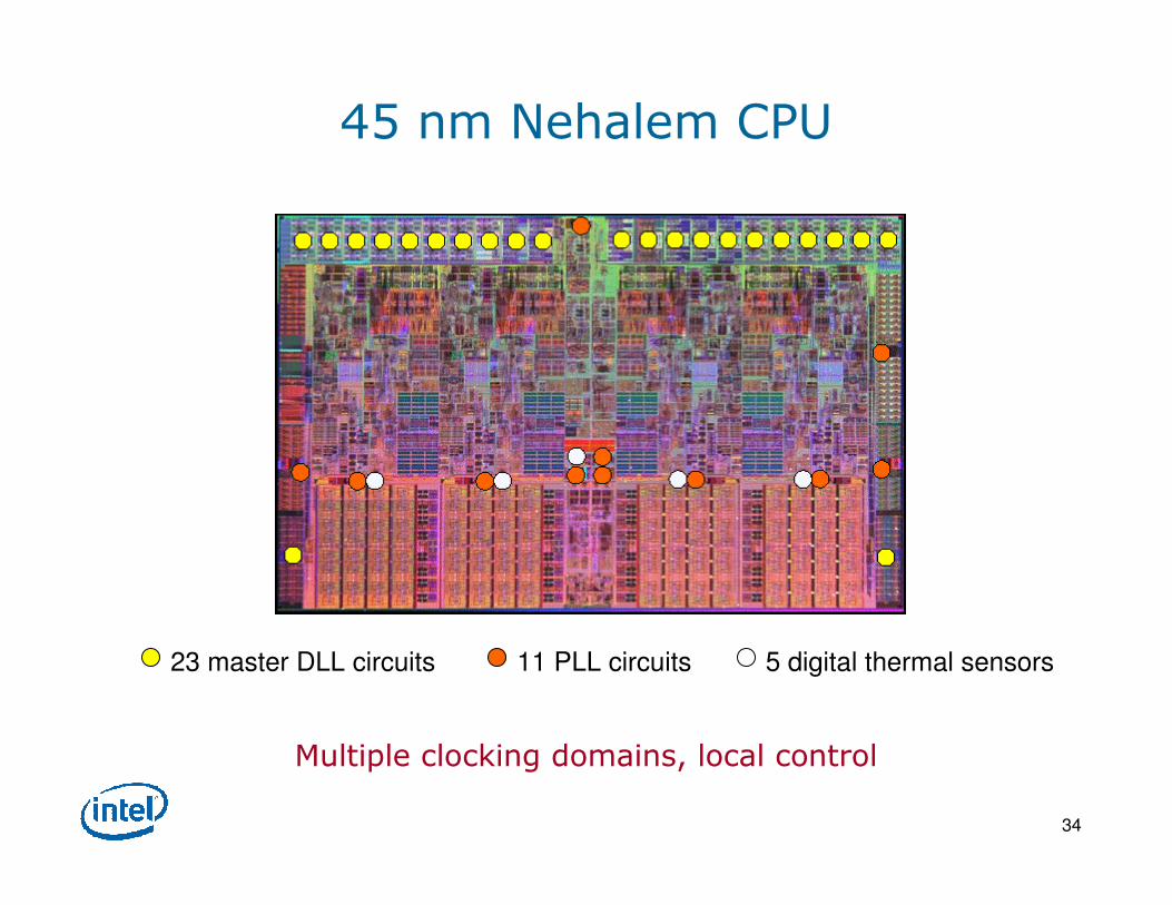
45 nm Nehalem CPU
11 PLL circuits 5 digital thermal sensors23 master DLL circuits
Multiple clocking domains, local control
35
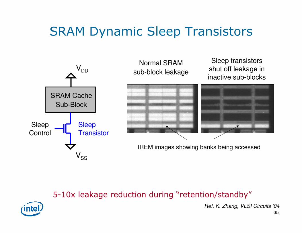
SRAM Dynamic Sleep Transistors
5-10x leakage reduction during “retention/standby”
IREM images showing banks being accessed
Normal SRAM
sub-block leakage
Sleep transistors
shut off leakage in
inactive sub-blocks
VSS
VDD
Sleep
Transistor
SRAM Cache
Sub-Block
Ref. K. Zhang, VLSI Circuits ‘04
Sleep
Control

36
Integrated Power Gates
• Shuts off both switching power and leakage power
• Enables idle cores to go to ~0 power, independent
of state of other cores on die
Core0 Core1 Core2 Core3
Memory System, Cache, I/O VTT
VCC
Nehalem
Power Gates
Thick On-Die (M9)
Interconnect Layer
Ref. R. Kumar, paper 3.2, ISSCC ’09

37
M9
M1-8
Thick metal 9 layer for low
resistance on-die power routing
Ultra-low leakage transistor for
high off-resistance power gates
Power Gates Enabled with Design+Process Co-optimization

38
Dynamically delivering optimal performance and energy efficiency
Nehalem Turbo ModeF
requency
Co
re 1
Co
re 2
Co
re 3
Co
re 0
• Power gates shut off some cores
• Zero power for inactive cores
• Higher frequency for active cores
• All cores operatingC
ore
1
Co
re 2
Co
re 3
Co
re 0
Co
re 1
Co
re 2
Co
re 3
Co
re 0
Ref. R. Kumar, paper 3.2, ISSCC ’09
Many threaded workloads Lightly threaded workloads - Turbo Mode

39
Nehalem Power Control Unit
PLL
UncoreLLC
Core 0
Vcc
Freq.
Sensors
Core 1
Vcc
Freq.
Sensors
Core 2
Vcc
Freq.
Sensors
Core 3
Vcc
Freq.
Sensors
PLL
PLL
PLL
PLL
PCU
BCLKVcc
� Integrated proprietary
microcontroller
� Shifts control from hardware to
embedded firmware
� Real time sensors for voltage,
temperature, current/power
� Flexibility enables sophisticated
algorithms, tuned for current
operating conditions
Ref. R. Kumar, paper 3.2, ISSCC ’09
40
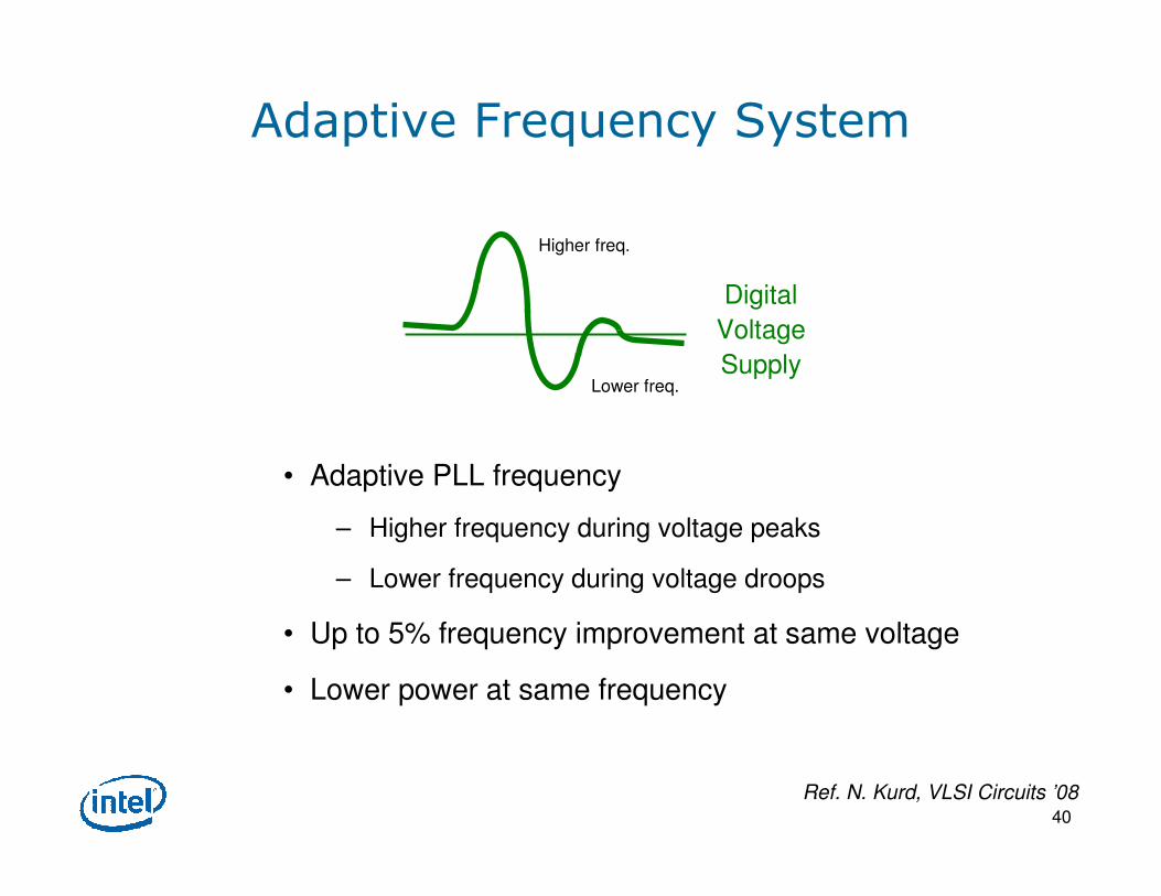
Adaptive Frequency System
• Adaptive PLL frequency
– Higher frequency during voltage peaks
– Lower frequency during voltage droops
• Up to 5% frequency improvement at same voltage
• Lower power at same frequency
Digital
Voltage
Supply
Higher freq.
Lower freq.
Ref. N. Kurd, VLSI Circuits ’08

41
PC Platform Comparison
Intel386TM
ProcessorCache Control
DRAM Control
Intel387 Math
Co-processor
DRAMDRAM
DRAMDRAM
Cache TAG
SRAM
Nehalem
Processor
DRAMDRAM
DRAMDRAM
1985 2008
Modern microprocessors integrate many of the
separate system components from past platforms
Cache Data
SRAM
Clock Gen.

42
Microprocessor Evolution
Intel386TM Nehalem
Transistor Count: 280 thousand 731 million
Frequency: 16 MHz >3.6 GHz
# Cores: 1 4
Cache Size: None 8 MB
I/O Peak Bandwidth: 64 MB/sec 50 GB/sec
Adaptive Circuits: None Sleep Mode
Turbo Mode
Power Gating
Adaptive Frequency Clocking

43
0.01
0.1
1
10
100
1000
0.4 0.6 0.8 1.0 1.2 1.4 1.6
ION (mA/um)
I OF
F (n
A/u
m) High
Perfomance
1.0V
Low
Power
1.1V
0.01
0.1
1
10
100
1000
0.6 0.8 1.0 1.2 1.4 1.6 1.8
ION (mA/um)
I OF
F (n
A/u
m) High
Performance
1.0V
Low
Power
1.1V
NMOS PMOS
45 nm SoC Transistors
Wider range of transistor types provided for SoC:
High performance and low power
Ref. C. Jan, IEDM ‘08
44
NMOS @ 1.8V
0.001
0.01
0.1
1
10
0.4 0.5 0.6 0.7 0.8
ION (mA/um)
I OF
F (n
A/u
m)
65nm
SiO2
45nm
HKMG
+17%
0.0001
0.001
0.01
0.1
1
0.2 0.3 0.4 0.5 0.6
ION (mA/um)
I OF
F (n
A/u
m)
45nm
HKMG
65nm
SiO2
PMOS @ 1.8V
+57%
45 nm SoC I/O Transistors
Wider range of transistor types provided for SoC:
High speed, high voltage I/O
Ref. C. Jan, IEDM ‘08
45
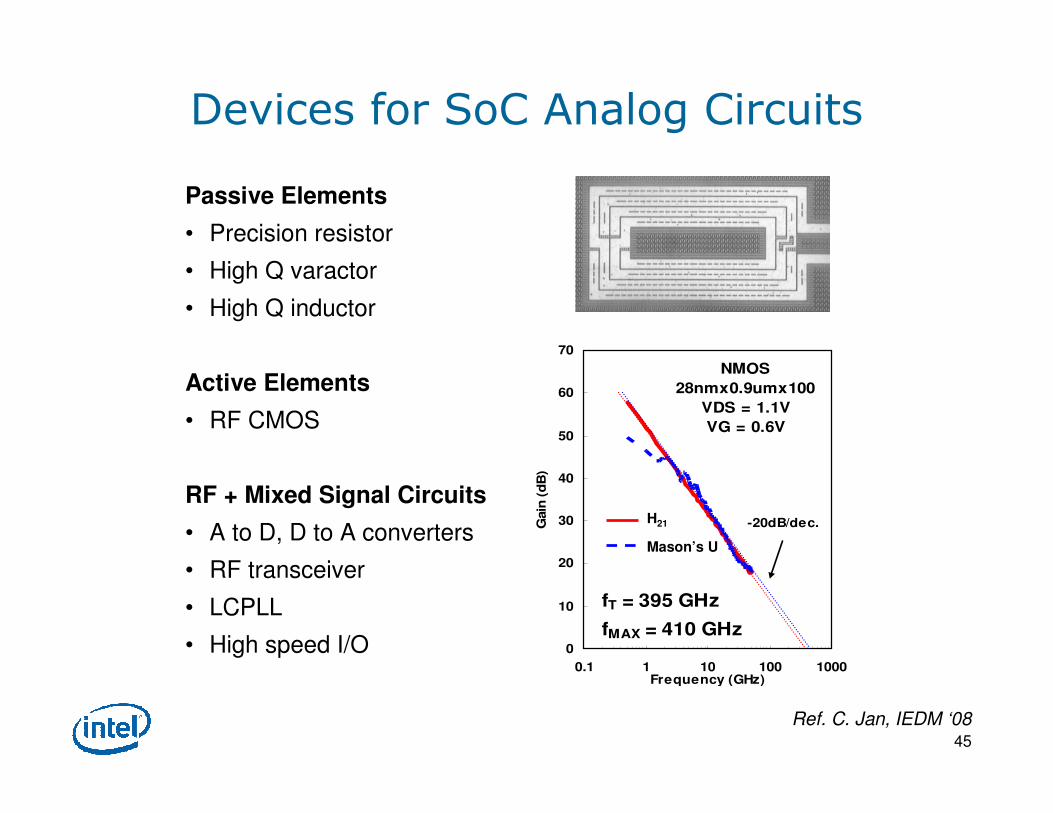
Devices for SoC Analog Circuits
0
10
20
30
40
50
60
70
0.1 1 10 100 1000Frequency (GHz)
Gain
(d
B)
-20dB/dec.
fT = 395 GHz
fMAX = 410 GHz
NMOS
28nmx0.9umx100
VDS = 1.1V
VG = 0.6V
H21
Mason’s U
Passive Elements
• Precision resistor
• High Q varactor
• High Q inductor
Active Elements
• RF CMOS
RF + Mixed Signal Circuits
• A to D, D to A converters
• RF transceiver
• LCPLL
• High speed I/O
Ref. C. Jan, IEDM ‘08

46
The Old Era of Microprocessor Scaling
Larger Cores
Higher Frequency
Higher Power
It has served us well for >30 years

47
The New Era of Microprocessor Scaling
Avoiding the power wall requires a systemic approach from
process technology through circuit design to micro-architecture
to deliver products with power efficient performance
Many-Core Multi-Core Multi-Function
System on a Chip

48
Outline
• Transistor Scaling
• Microprocessor Evolution
• Vision of the Future

49
Future Scaling Challenges
• Patterning ever-smaller features sizes
• Transistor and interconnect technologies that
provide higher performance at lower power
• Continued voltage scaling for low power
• Integrating a wider range of device types for
system-on-chip or system-in-package products

50
0.01
0.1
1
1980 1990 2000 2010 2020
micron
10
100
1000
nm
32nm
22nm
15nm
Feature Size
Wavelength
248nm193nm
EUV
13.5nm
OPC
Phase shift
Immersion
Lithography
193 nm enhancements got us to the 32 nm generation

51
Layout Restrictions
65 nm Layout Style 32 nm Layout Style
• Bi-directional features
• Varied gate dimensions
• Varied pitches
• Uni-directional features
• Uniform gate dimension
• Gridded layout

52
Lithography Options for Beyond 32 nm
Pixilated Mask Printed Image
Pitch Doubling 2-D Features
Double Patterning
• Pitch doubling
• Improved 2-D features
Computational Lithography
• Pixilated mask
• Existing 193 nm litho tools

53
Extreme Ultraviolet Lithography
Intel EUV Mask
C
2H2H2H2H 08080808
2007200720072007
1H1H1H1H’’’’08080808
TargetTargetTargetTarget
2H2H2H2H’’’’08080808
Continued progress towards EUV implementation
Photoresist Development Nikon EUV1 printed wafer
ASML ADT printed wafer
Philips beta source
Cymer beta source

54
Transistor Options
(110)
<100>
<110>
<111>(100)
<110>
<110>
<100>
Substrate Engineering
+ Increased p-channel mobility
? Impact on n-channel mobility
Multi-Gate FETs
+ Improved electrostatics
+ Steeper sub-threshold slope
? Higher parasitic resistance
? Higher parasitic capacitance
FinFET
GAA
40
90
140
190
240
290
340
-3000 -2000 -1000 0
<110> Stress (MPa)
Hole
Mobili
ty (
cm
2/V
s)
(100) Mobility(110) Mobility
Hole
40
90
140
190
240
290
340
-3000 -2000 -1000 0
<110> Stress (MPa)
Hole
Mobili
ty (
cm
2/V
s)
(100) Mobility(110) Mobility
Hole
2x
55
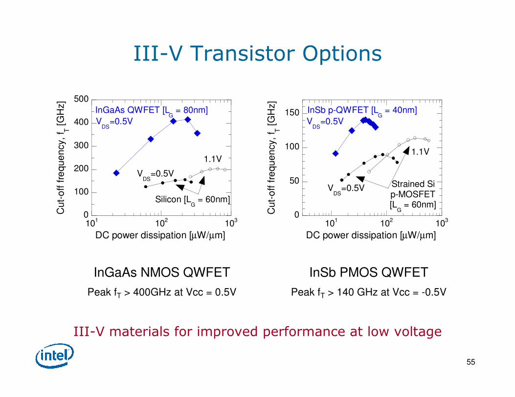
III-V Transistor Options
InSb PMOS QWFET
Peak fT > 140 GHz at Vcc = -0.5V
InGaAs NMOS QWFET
Peak fT > 400GHz at Vcc = 0.5V
0
50
100
150
101
102
103
Cut-
off
fre
qu
en
cy,
f T [
GH
z]
DC power dissipation [µW/µm]
VDS
=0.5V
VDS
=0.5V
1.1V
Strained Sip-MOSFET[L
G = 60nm]
InSb p-QWFET [LG = 40nm]
0
100
200
300
400
500
101
102
103
Cut-
off
fre
qu
en
cy,
f T [
GH
z]
DC power dissipation [µW/µm]
VDS
=0.5V
VDS
=0.5V
1.1V
Silicon [LG = 60nm]
InGaAs QWFET [LG = 80nm]
III-V materials for improved performance at low voltage

56
3-D Chip Stacking
Top Chip
Bottom Chip
Package
+ High density chip-chip
connections
+ Small form factor
+ Combine dissimilar
technologies
? Added cost
? Degraded power delivery,
heat sinking
? Area impact on lower chip
Package
TSV
3-D chip stacking using through-silicon vias
CPU
MemoryTSV

57
Optical Interconnects
Ref. I. Young, paper 28.1, ISSCC ’09
Nearer term: High bandwidth chip-chip interconnects
Longer term: On-chip interconnects
Chip (CPU, Memory, Graphics, etc.)
Laser
Modulators
Ge Photodetectors
Waveguides
Optical Layer
Optical Layer
Chip
Optical Layer
Chip
Optical
Interconnects
LaserLaser
58
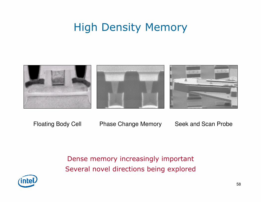
High Density Memory
Seek and Scan Probe Floating Body Cell Phase Change Memory
Dense memory increasingly important
Several novel directions being explored
59
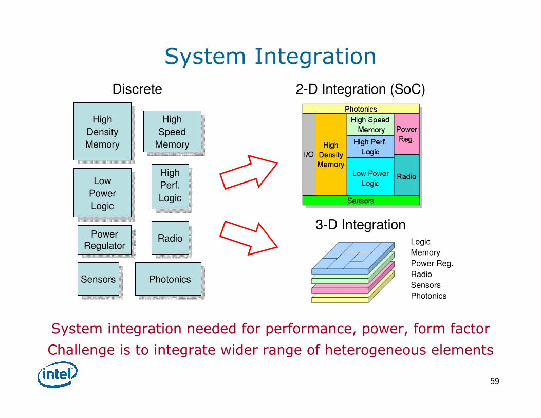
System Integration
High
Perf.
Logic
Low
Power
Logic
High
Speed
Memory
High
Density
Memory
Sensors
RadioPower Regulator Logic
Memory
Power Reg.
Radio
Sensors
Photonics
System integration needed for performance, power, form factor
Challenge is to integrate wider range of heterogeneous elements
Discrete 2-D Integration (SoC)
3-D Integration
Photonics
60
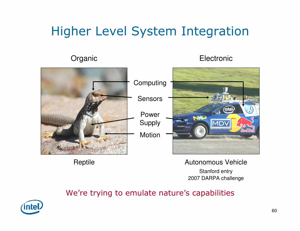
Higher Level System Integration
ElectronicOrganic
Reptile Autonomous Vehicle
Stanford entry
2007 DARPA challenge
Computing
Sensors
Power
Supply
Motion
We’re trying to emulate nature’s capabilities

61
Evolutionary Comparison
Transistor Integrated Circuit
Microprocessor PC
Autonomous Vehicle
Electronic
Organic
Human
What did nature have to “invent” to evolve to higher forms?
Multi-Cell Organism
Complex Molecule
Single-Cell Organism
Reptile
Robot

62
Brain Neuron
Up to 1 meter in length
~50 um
Output
Input
Neuron Transistor
Charge carrier: Ions Electrons
Voltage swing: 100 mV 1.0 V
Threshold voltage: 10-20 mV ~300 mV
Nature is a master of low power operation
Neuron image from J. Nolte [36]
63
Organic vs. Electronic Circuits
Brain circuits are slow but massively parallel
AND/OR Function
FI, FO ~1000
Operates ~100 Hz
Neuron image from J. Nolte [36]

64
Cu Wire
Repeater
Low-k
0.5 mm
Cu + Low-k + Repeaters >107 m/sec
Organic vs. Electronic Interconnects
Myelin coating improves axon signal speed ~10x, but still slow
1.0 mm
Myelinated Axon 25 m/sec
Cu Wire
Low-k
Repeater
Axon image from J. Nolte [36]

65
Organic vs. Electronic Systems
We have a way to go and much to learn
>108 CPU Transistors
1011 System Total
Keyboard, Radio,
USB Port
>2 GHz
40 Watts
1011 Neurons
1014 Synapses
Eyes, Ears, Taste,
Touch, Smell
100 Hz
20 Watts
# Devices:
Input Devices:
Operating Freq:
Power:
�
�
�
�
66
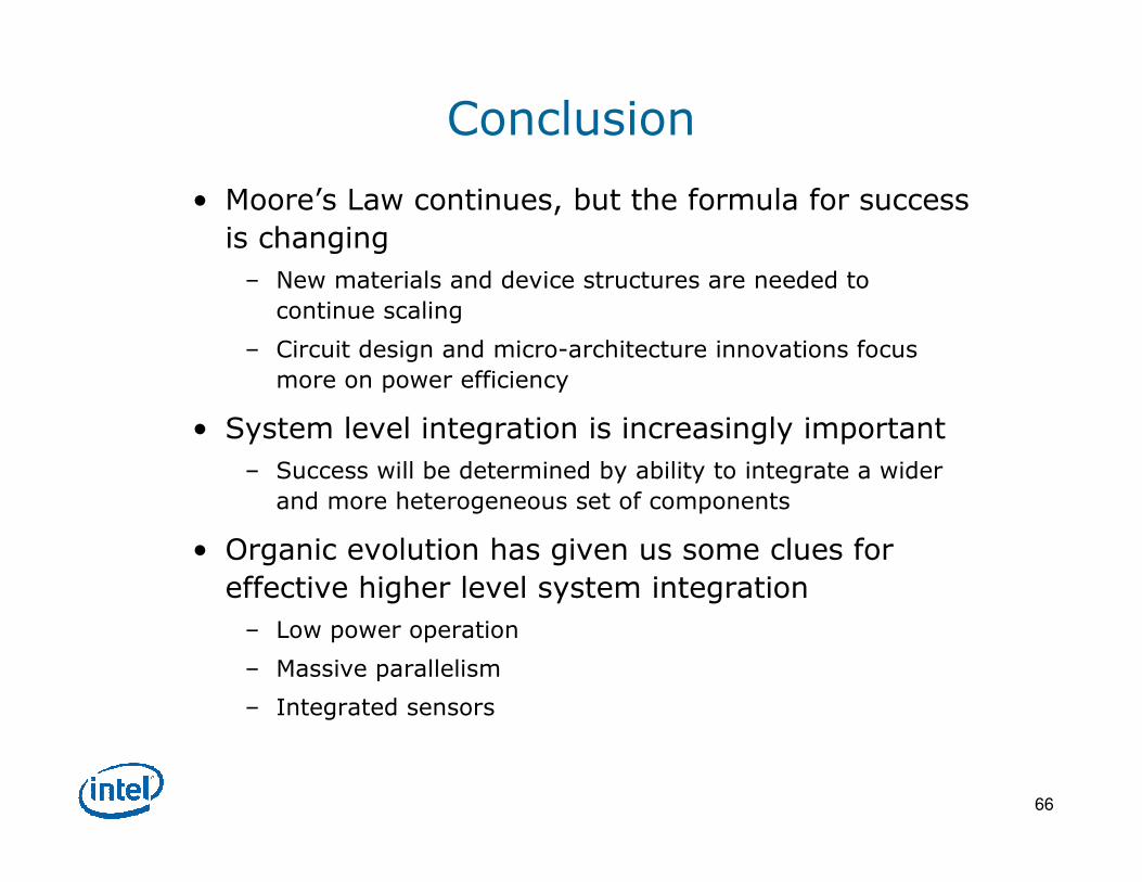
Conclusion
• Moore’s Law continues, but the formula for success
is changing
– New materials and device structures are needed to
continue scaling
– Circuit design and micro-architecture innovations focus
more on power efficiency
• System level integration is increasingly important
– Success will be determined by ability to integrate a wider
and more heterogeneous set of components
• Organic evolution has given us some clues for
effective higher level system integration
– Low power operation
– Massive parallelism
– Integrated sensors