ia82050 asynchronous serial controller data sheet - · pdf fileasynchronous serial controller...
TRANSCRIPT
IA82050 Data Sheet Asynchronous Serial Controller January 9, 2015
IA211030617-09 http://www.Innovasic.com UNCONTROLLED WHEN PRINTED OR COPIED Customer Support: Page 1 of 22 1-888-824-4184
®
IA82050 Asynchronous Serial Controller Data Sheet
®

IA82050 Data Sheet Asynchronous Serial Controller January 9, 2015
IA211030617-09 http://www.Innovasic.com UNCONTROLLED WHEN PRINTED OR COPIED Customer Support: Page 2 of 22 1-888-824-4184
®
Copyright 2008 by Innovasic Semiconductor, Inc.
Published by Innovasic Semiconductor, Inc. 3737 Princeton Drive NE, Suite 130, Albuquerque, NM 87107
Intel is a registered trademark of Intel Corporation MILES™ is a trademark of Innovasic Semiconductor, Inc.
IA82050 Data Sheet Asynchronous Serial Controller January 9, 2015
IA211030617-09 http://www.Innovasic.com UNCONTROLLED WHEN PRINTED OR COPIED Customer Support: Page 3 of 22 1-888-824-4184
®
TABLE OF CONTENTS
List of Figures ..................................................................................................................................4 List of Tables ...................................................................................................................................4 1. Features ...................................................................................................................................5 2. Description ..............................................................................................................................7 3. Functional Overview ..............................................................................................................9
3.1 Transmitter ....................................................................................................................9 3.2 Receiver .........................................................................................................................9 3.3 Bus Interface .................................................................................................................9 3.4 Register Description ....................................................................................................10
4. Register Descriptions ............................................................................................................11
4.1 Baud Rate Generator A Divide Count, MSB and LSB (BAH/BAL) ..........................11 4.2 General Interrupt Enable Register (GER) ...................................................................11
4.3 General Interrupt Register (GIR) ................................................................................11 4.4 Line Configure Register (LCR) ...................................................................................11
4.5 Line Status Register (LSR) .........................................................................................12 4.6 Modem Control Register (MCR) ................................................................................12 4.7 Modem Status Register (MSR) ...................................................................................13
4.8 Receive Data Register (RXDATA) .............................................................................13 4.9 Scratch Register (SCR) ...............................................................................................13
4.10 Transmit Data Register (TXDATA) ...........................................................................14 5. AC/DC Parameters ...............................................................................................................15 6. DC Characteristics ................................................................................................................16
7. AC Characteristics ................................................................................................................17
8. Packaging Information ..........................................................................................................18
8.1 PDIP Package ..............................................................................................................18 8.2 PLCC Package .............................................................................................................19
9. Innovasic Part Number Cross-Reference ..............................................................................20 10. Revision History ...................................................................................................................21 11. For Additional Information ...................................................................................................22

IA82050 Data Sheet Asynchronous Serial Controller January 9, 2015
IA211030617-09 http://www.Innovasic.com UNCONTROLLED WHEN PRINTED OR COPIED Customer Support: Page 4 of 22 1-888-824-4184
®
LIST OF FIGURES
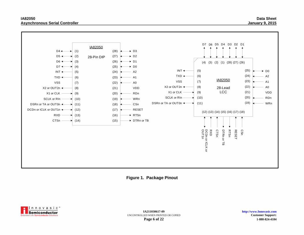
Figure 1. Package Pinout ................................................................................................................6
Figure 2. Functional Block Diagram ..............................................................................................8 Figure 3. PDW Physical Package Dimensions .............................................................................18 Figure 4. PLCC Physical Package Dimensions ............................................................................19
LIST OF TABLES
Table 1. Register Summary...........................................................................................................10
Table 2. General Interrupt Enable Register ..................................................................................11
Table 3. General Interrupt Register ..............................................................................................11 Table 4. Line Configure Register ..................................................................................................12 Table 5. Line Status Register ........................................................................................................12
Table 6. Modem Control Register ................................................................................................13 Table 7. Modem Status Register ...................................................................................................13 Table 8. AC/DC Parameters .........................................................................................................15
Table 9. DC Characteristics ..........................................................................................................16 Table 10. AC Characteristics ........................................................................................................17
Table 11. Innovasic Part Number Cross-Reference for the PDIP ................................................20 Table 12. Innovasic Part Number Cross-Reference for the PLCC ...............................................20
IA82050 Data Sheet Asynchronous Serial Controller January 9, 2015
IA211030617-09 http://www.Innovasic.com UNCONTROLLED WHEN PRINTED OR COPIED Customer Support: Page 5 of 22 1-888-824-4184
®
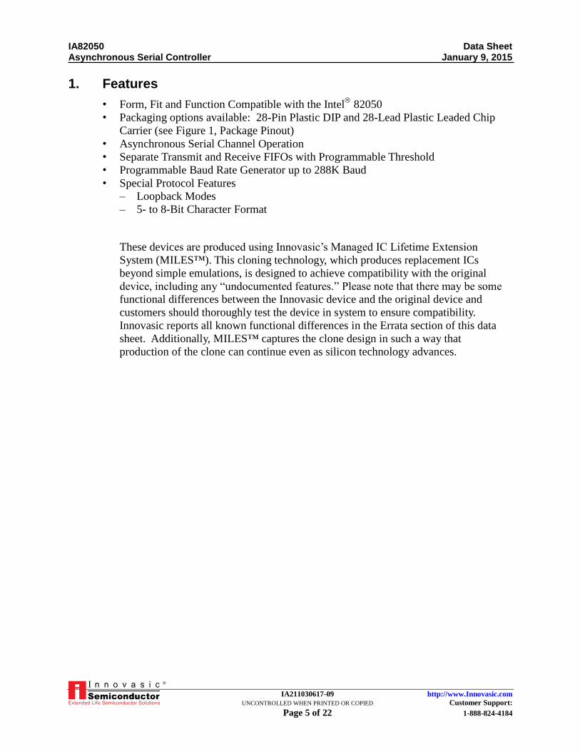
1. Features
• Form, Fit and Function Compatible with the Intel
82050
• Packaging options available: 28-Pin Plastic DIP and 28-Lead Plastic Leaded Chip
Carrier (see Figure 1, Package Pinout)
• Asynchronous Serial Channel Operation
• Separate Transmit and Receive FIFOs with Programmable Threshold
• Programmable Baud Rate Generator up to 288K Baud
• Special Protocol Features
– Loopback Modes
– 5- to 8-Bit Character Format
These devices are produced using Innovasic’s Managed IC Lifetime Extension
System (MILES™). This cloning technology, which produces replacement ICs
beyond simple emulations, is designed to achieve compatibility with the original
device, including any “undocumented features.” Please note that there may be some
functional differences between the Innovasic device and the original device and
customers should thoroughly test the device in system to ensure compatibility.
Innovasic reports all known functional differences in the Errata section of this data
sheet. Additionally, MILES™ captures the clone design in such a way that
production of the clone can continue even as silicon technology advances.
IA82050 Data Sheet Asynchronous Serial Controller January 9, 2015
IA211030617-09 http://www.Innovasic.com UNCONTROLLED WHEN PRINTED OR COPIED Customer Support: Page 6 of 22 1-888-824-4184
®
Figure 1. Package Pinout
(6)TXD
(1)D4
(2)D5
(3)D6
(4)D7
(5)INT
(7)VSS
(8)X2 or OUT2n
(9)X1 or CLK
(10)SCLK or RIn
(11)DSRn or TA or OUT0n
(12)DCDn or ICLK or OUT1n
(13)RXD
(14)CTSn
(28) D3
(27) D2
(26) D1
(25) D0
(24) A2
(23) A1
(22) A0
(21) VDD
(20) RDn
(19) WRn
(18) CSn
(17) RESET
(16) RTSn
(15) DTRn or TB
(6)TXD
(5)INT
(7)VSS
(8)X2 or OUT2n
(9)X1 or CLK
(10)SCLK or RIn
(11)DSRn or TA or OUT0n
(25) D0
(24) A2
(23) A1
(22) A0
(21) VDD
(20) RDn
(19) WRn
(4)
D7
(3)
D6
(2)
D5
(1)
D4
(28)
D3
(27)
D2
(26)
D1
(18)
CS
n
(17)
RE
SE
T
(16)
RT
Sn
(15)
DT
Rn
or T
B
(14)
CT
Sn
(13)
RX
D
(12)
DC
Dn
or IC
LK
or
OU
T1n
28-Pin DIP
IA82050
28-Lead
LCC
IA82050
IA82050 Data Sheet Asynchronous Serial Controller February 25, 2011
IA211030617-09 http://www.Innovasic.com UNCONTROLLED WHEN PRINTED OR COPIED Customer Support: Page 7 of 22 1-888-824-4184
®
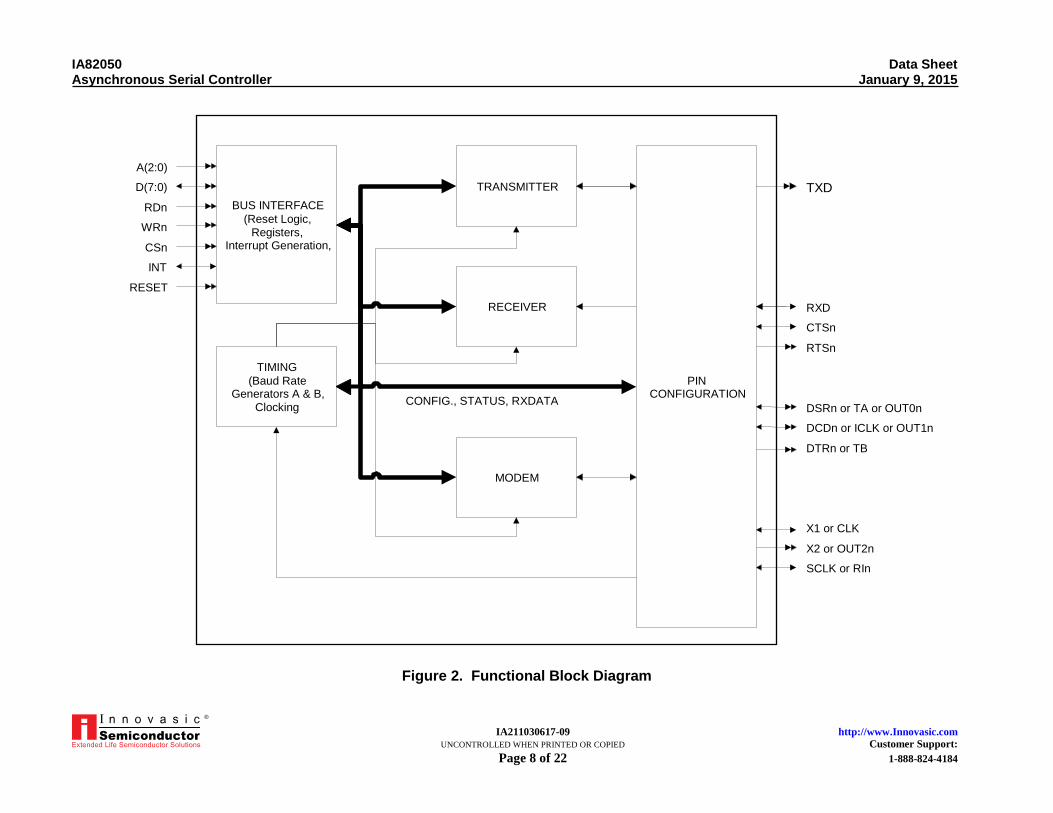
2. Description
The IA82050 is an asynchronous serial controller that provides a CPU interface to one transmit
and one receive channel. It is form, fit, and function compatible with the Intel® 82050 and
82510. Configuration registers are used to control the serial channel, interrupts, and modes of
operation. The CPU controls this device via address and data lines with read/write control. The
CPU also uses this interface to read and write data to receive and transmit data through the serial
channel. FIFOs and various serial modes can be used to help off-load the CPU from transmitting
and receiving data. An interrupt line provides an indication to the CPU that the device requires
servicing. The device can be configured for 8250A/16450 compatibility. See Figure 2,
Functional Block Diagram.
IA82050 Data Sheet Asynchronous Serial Controller January 9, 2015
IA211030617-09 http://www.Innovasic.com UNCONTROLLED WHEN PRINTED OR COPIED Customer Support: Page 8 of 22 1-888-824-4184
®
Figure 2. Functional Block Diagram
IA82510
BUS INTERFACE (Reset Logic,
Registers, Interrupt Generation,
CONFIG., STATUS, RXDATA TXDATA
TIMING (Baud Rate
Generators A & B, Clocking
PIN CONFIGURATION
RECEIVER
TRANSMITTER
MODEM
TXD
RXD
X2 or OUT2n
SCLK or RIn
X1 or CLK
RTSn
CTSn
DSRn or TA or OUT0n
DCDn or ICLK or OUT1n
DTRn or TB
A(2:0)
D(7:0)
RDn
WRn
CSn
INT
RESET
IA82050 Data Sheet Asynchronous Serial Controller January 9, 2015
IA211030617-09 http://www.Innovasic.com UNCONTROLLED WHEN PRINTED OR COPIED Customer Support: Page 9 of 22 1-888-824-4184
®
3. Functional Overview
3.1 Transmitter
The Transmit function consists of a one-character FIFO, and a Transmit Engine. The transmit
engine is responsible for reading the data out of the FIFO and placing it in the proper order on
the TXD pin. The transmit engine is highly configurable to be compatible with numerous
formats, including 16450 and 8250 modes of communication. Transmit Communication
parameters that can be programmed include:
• Parity modes
• Stop Bits
• Character Length
For more details, see Chapter 5, Register Descriptions.
3.2 Receiver
The Receiver function consists of a one-character FIFO and a receive engine. The receive
engine is responsible for sampling the data on the RXD input pin, formatting the data, and
placing the data in the FIFO. The receive engine is highly configurable with parameters that
include:
• Parity modes
• Stop Bits
• Character Length
For more details, see Chapter 5, Register Descriptions.
3.3 Bus Interface
The Bus Interface is a simple interface that allows a micro-processor or micro-controller to read
and write the IA82050 Registers. It consists of the following I/O lines:
• A0, A1, A2 : 3-Bit Address
• D0-D7 : 8-Bit Data
• RDn: Active Low Read Enable
• WRn: Active Low Write Enable
• CSn: Active Low Chip Select
• INT: Interrupt Output
• RESET: Chip Reset
IA82050 Data Sheet Asynchronous Serial Controller January 9, 2015
IA211030617-09 http://www.Innovasic.com UNCONTROLLED WHEN PRINTED OR COPIED Customer Support: Page 10 of 22 1-888-824-4184
®
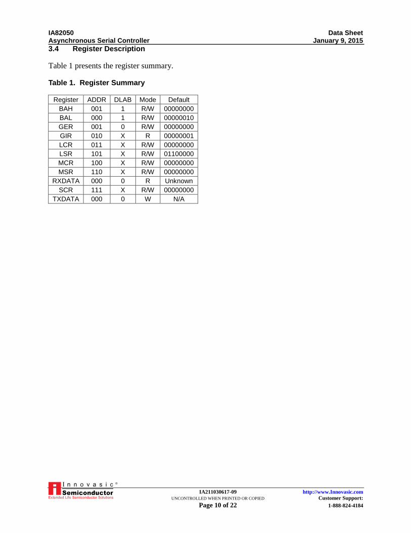
3.4 Register Description
Table 1 presents the register summary.
Table 1. Register Summary
Register ADDR DLAB Mode Default
BAH 001 1 R/W 00000000
BAL 000 1 R/W 00000010
GER 001 0 R/W 00000000
GIR 010 X R 00000001
LCR 011 X R/W 00000000
LSR 101 X R/W 01100000
MCR 100 X R/W 00000000
MSR 110 X R/W 00000000
RXDATA 000 0 R Unknown
SCR 111 X R/W 00000000
TXDATA 000 0 W N/A
IA82050 Data Sheet Asynchronous Serial Controller January 9, 2015
IA211030617-09 http://www.Innovasic.com UNCONTROLLED WHEN PRINTED OR COPIED Customer Support: Page 11 of 22 1-888-824-4184
®
4. Register Descriptions
4.1 Baud Rate Generator A Divide Count, MSB and LSB (BAH/BAL)
Baud Rate Generator A Divide Count (MSB and LSB) – When generating TXCLK or RXCLK,
the selected source clock will be divided by this value (ADDR 001/000, Mode R/W, Default
00000000/00000010).
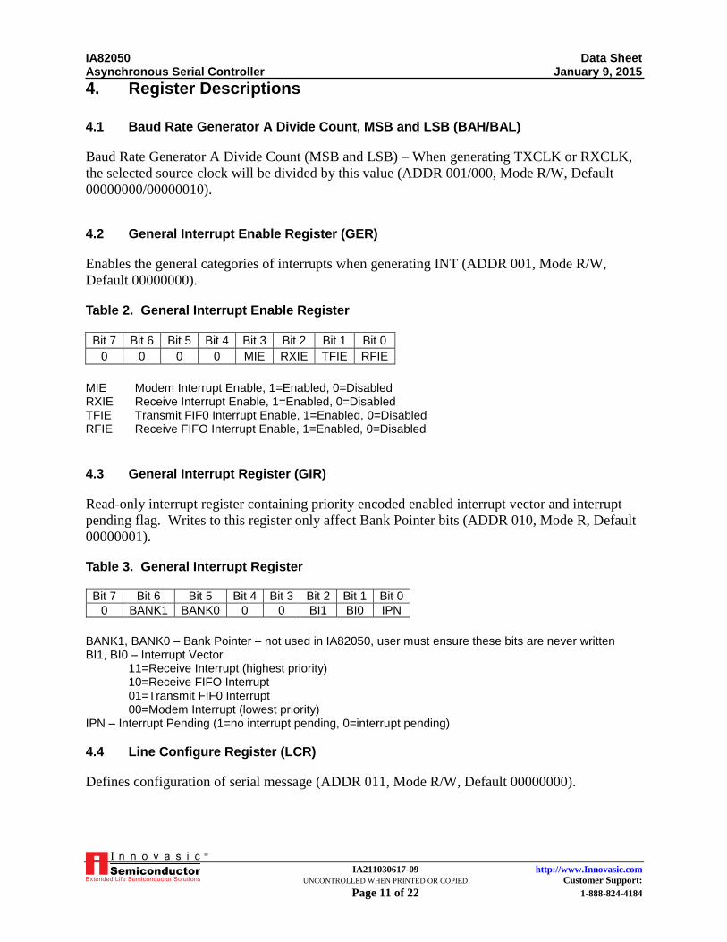
4.2 General Interrupt Enable Register (GER)
Enables the general categories of interrupts when generating INT (ADDR 001, Mode R/W,
Default 00000000).
Table 2. General Interrupt Enable Register
Bit 7 Bit 6 Bit 5 Bit 4 Bit 3 Bit 2 Bit 1 Bit 0
0 0 0 0 MIE RXIE TFIE RFIE
MIE Modem Interrupt Enable, 1=Enabled, 0=Disabled RXIE Receive Interrupt Enable, 1=Enabled, 0=Disabled TFIE Transmit FIF0 Interrupt Enable, 1=Enabled, 0=Disabled RFIE Receive FIFO Interrupt Enable, 1=Enabled, 0=Disabled
4.3 General Interrupt Register (GIR)
Read-only interrupt register containing priority encoded enabled interrupt vector and interrupt
pending flag. Writes to this register only affect Bank Pointer bits (ADDR 010, Mode R, Default
00000001).
Table 3. General Interrupt Register
Bit 7 Bit 6 Bit 5 Bit 4 Bit 3 Bit 2 Bit 1 Bit 0
0 BANK1 BANK0 0 0 BI1 BI0 IPN
BANK1, BANK0 – Bank Pointer – not used in IA82050, user must ensure these bits are never written BI1, BI0 – Interrupt Vector 11=Receive Interrupt (highest priority) 10=Receive FIFO Interrupt 01=Transmit FIF0 Interrupt 00=Modem Interrupt (lowest priority) IPN – Interrupt Pending (1=no interrupt pending, 0=interrupt pending)
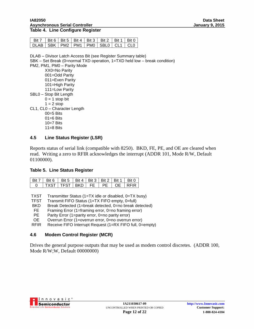
4.4 Line Configure Register (LCR)
Defines configuration of serial message (ADDR 011, Mode R/W, Default 00000000).
IA82050 Data Sheet Asynchronous Serial Controller January 9, 2015
IA211030617-09 http://www.Innovasic.com UNCONTROLLED WHEN PRINTED OR COPIED Customer Support: Page 12 of 22 1-888-824-4184
®
Table 4. Line Configure Register
Bit 7 Bit 6 Bit 5 Bit 4 Bit 3 Bit 2 Bit 1 Bit 0
DLAB SBK PM2 PM1 PM0 SBL0 CL1 CL0
DLAB – Divisor Latch Access Bit (see Register Summary table) SBK – Set Break (0=normal TXD operation, 1=TXD held low – break condition) PM2, PM1, PM0 – Parity Mode XX0=No Parity 001=Odd Parity 011=Even Parity 101=High Parity 111=Low Parity SBL0 – Stop Bit Length 0 = 1 stop bit 1 = 2 stop CL1, CL0 – Character Length 00=5 Bits 01=6 Bits 10=7 Bits 11=8 Bits
4.5 Line Status Register (LSR)
Reports status of serial link (compatible with 8250). BKD, FE, PE, and OE are cleared when
read. Writing a zero to RFIR acknowledges the interrupt (ADDR 101, Mode R/W, Default
01100000).
Table 5. Line Status Register
Bit 7 Bit 6 Bit 5 Bit 4 Bit 3 Bit 2 Bit 1 Bit 0
0 TXST TFST BKD FE PE OE RFIR
TXST Transmitter Status (1=TX idle or disabled, 0=TX busy) TFST Transmit FIFO Status (1=TX FIFO empty, 0=full) BKD Break Detected (1=break detected, 0=no break detected) FE Framing Error (1=framing error, 0=no framing error) PE Parity Error (1=parity error, 0=no parity error) OE Overrun Error (1=overrun error, 0=no overrun error)
RFIR Receive FIFO Interrupt Request (1=RX FIFO full, 0=empty)
4.6 Modem Control Register (MCR)
Drives the general purpose outputs that may be used as modem control discretes. (ADDR 100,
Mode R/W;W, Default 00000000)
IA82050 Data Sheet Asynchronous Serial Controller January 9, 2015
IA211030617-09 http://www.Innovasic.com UNCONTROLLED WHEN PRINTED OR COPIED Customer Support: Page 13 of 22 1-888-824-4184
®
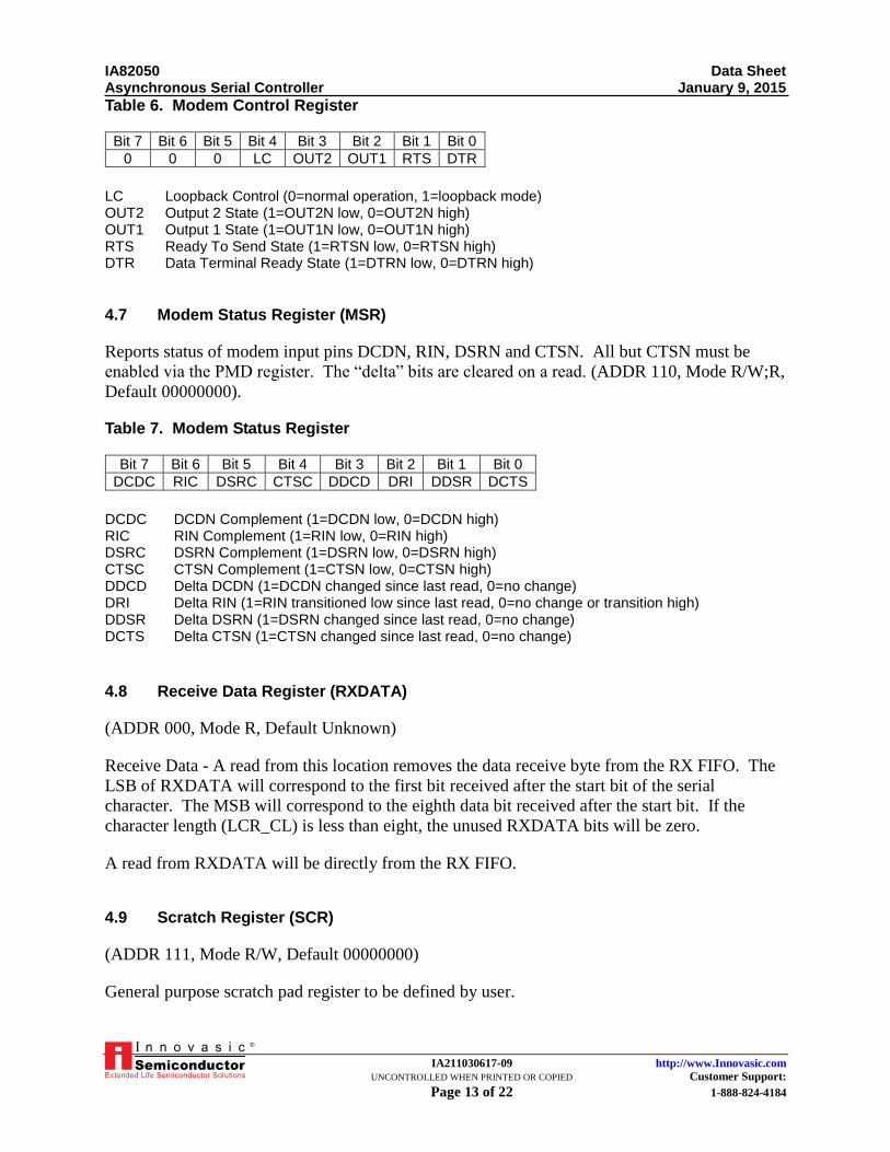
Table 6. Modem Control Register
Bit 7 Bit 6 Bit 5 Bit 4 Bit 3 Bit 2 Bit 1 Bit 0
0 0 0 LC OUT2 OUT1 RTS DTR
LC Loopback Control (0=normal operation, 1=loopback mode) OUT2 Output 2 State (1=OUT2N low, 0=OUT2N high) OUT1 Output 1 State (1=OUT1N low, 0=OUT1N high) RTS Ready To Send State (1=RTSN low, 0=RTSN high) DTR Data Terminal Ready State (1=DTRN low, 0=DTRN high)
4.7 Modem Status Register (MSR)
Reports status of modem input pins DCDN, RIN, DSRN and CTSN. All but CTSN must be
enabled via the PMD register. The “delta” bits are cleared on a read. (ADDR 110, Mode R/W;R,
Default 00000000).
Table 7. Modem Status Register
Bit 7 Bit 6 Bit 5 Bit 4 Bit 3 Bit 2 Bit 1 Bit 0
DCDC RIC DSRC CTSC DDCD DRI DDSR DCTS
DCDC DCDN Complement (1=DCDN low, 0=DCDN high) RIC RIN Complement (1=RIN low, 0=RIN high) DSRC DSRN Complement (1=DSRN low, 0=DSRN high) CTSC CTSN Complement (1=CTSN low, 0=CTSN high) DDCD Delta DCDN (1=DCDN changed since last read, 0=no change) DRI Delta RIN (1=RIN transitioned low since last read, 0=no change or transition high) DDSR Delta DSRN (1=DSRN changed since last read, 0=no change) DCTS Delta CTSN (1=CTSN changed since last read, 0=no change)
4.8 Receive Data Register (RXDATA)
(ADDR 000, Mode R, Default Unknown)
Receive Data - A read from this location removes the data receive byte from the RX FIFO. The
LSB of RXDATA will correspond to the first bit received after the start bit of the serial
character. The MSB will correspond to the eighth data bit received after the start bit. If the
character length (LCR_CL) is less than eight, the unused RXDATA bits will be zero.
A read from RXDATA will be directly from the RX FIFO.
4.9 Scratch Register (SCR)
(ADDR 111, Mode R/W, Default 00000000)
General purpose scratch pad register to be defined by user.
IA82050 Data Sheet Asynchronous Serial Controller January 9, 2015
IA211030617-09 http://www.Innovasic.com UNCONTROLLED WHEN PRINTED OR COPIED Customer Support: Page 14 of 22 1-888-824-4184
®
4.10 Transmit Data Register (TXDATA)
(ADDR 000, Mode W, Default N/A)
Transmit Data - A write to this location adds a data byte to the TX FIFO, and initiates the
transmit sequence.
IA82050 Data Sheet Asynchronous Serial Controller January 9, 2015
IA211030617-09 http://www.Innovasic.com UNCONTROLLED WHEN PRINTED OR COPIED Customer Support: Page 15 of 22 1-888-824-4184
®
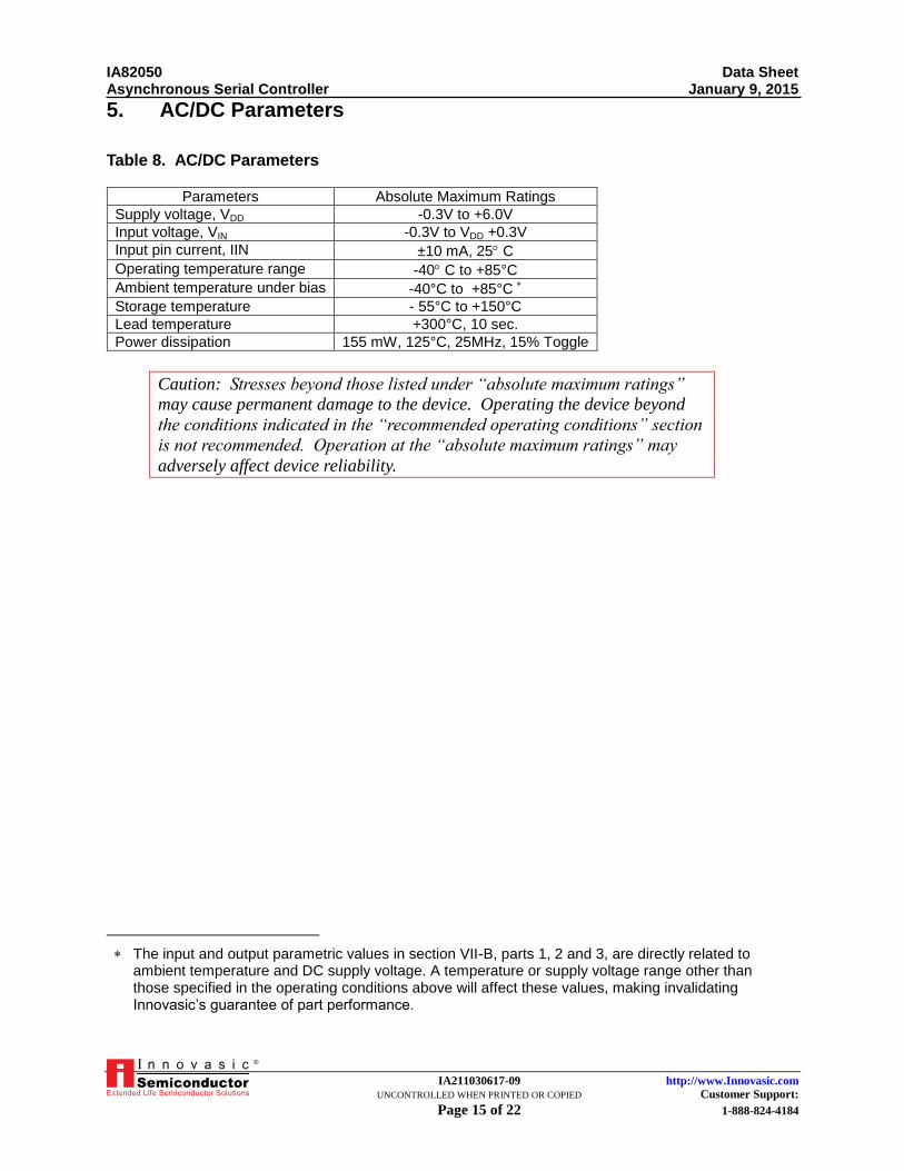
5. AC/DC Parameters
Table 8. AC/DC Parameters
Parameters Absolute Maximum Ratings
Supply voltage, VDD -0.3V to +6.0V
Input voltage, VIN -0.3V to VDD +0.3V
Input pin current, IIN ±10 mA, 25 C
Operating temperature range -40 C to +85°C
Ambient temperature under bias -40°C to +85°C
Storage temperature - 55°C to +150°C
Lead temperature +300°C, 10 sec.
Power dissipation 155 mW, 125°C, 25MHz, 15% Toggle
Caution: Stresses beyond those listed under “absolute maximum ratings”
may cause permanent damage to the device. Operating the device beyond
the conditions indicated in the “recommended operating conditions” section
is not recommended. Operation at the “absolute maximum ratings” may
adversely affect device reliability.
The input and output parametric values in section VII-B, parts 1, 2 and 3, are directly related to
ambient temperature and DC supply voltage. A temperature or supply voltage range other than those specified in the operating conditions above will affect these values, making invalidating Innovasic’s guarantee of part performance.

IA82050 Data Sheet Asynchronous Serial Controller January 9, 2015
IA211030617-09 http://www.Innovasic.com UNCONTROLLED WHEN PRINTED OR COPIED Customer Support: Page 16 of 22 1-888-824-4184
®
6. DC Characteristics
Table 9. DC Characteristics
Symbol Parameter Notes Min Max Unit
VIL Input Low Voltage (1) -0.5 0.3 V
VIH1 Input High Voltage-Cerdip (1) 2.1 VDD+.3 V
VIH2 Input High Voltage-LCC (2) 2.1 VDD+.3 V
VOL Output Low Voltage (2),(8) 0.4 V
VOH Output High Voltage (3),(8) 2.4 V
ILI Input Leakage Current (4) 1 A
ILO 3-State Leakage Current (5) 10 A
ICC Power Supply Current (6) 1.12 mA/MHz
IPU Strapping Pullup Resistor (12) -28.3 -137 A
ISTBY Standby Supply Current (9) 100 A
IOHR RTSn, DTRn Strapping Current (10) 1.92 mA
IOLR RTSn, DTRn Strapping Current (11) N/A mA
CIN Input Capacitance (7) 5 pF
CIO I/O Capacitance (7) 6 pF
CXTAL X1, X2 Load 6 pF
Notes: 1. Does not apply to CLK/X1 pin, when configured as crystal oscillator input (X1). 2. @IOL = 1.92 mA 3. @IOH = 1.92 mA 4. 0< VIN <VCC 5. 0.4V < VOUT < VCC – 0.4V 6. VDD = 5.5V, VIL = 0.7V (max), VIH = VDD – 0.7V (min), Typ. Val = 1.12 mA/MHz (Not Tested), Ext.
1X CLK, IOL = IOH = 0 7. Freq. = 1 MHz 8. Does not apply to OUT2/X2 pin, when configured as crystal oscillator output (X2). 9. Freq. = 1 MHz, but input clock not running. Static IDD current is exclusive of input/output drive
requirements and is measured with the clocks stopped and all inputs tied to VDD or VSS, configured to draw minimum current.
10. Applies only during hardware reset for clock configuration options. Strapping current for logic HIGH. 11. Applies only during hardware reset for clock configuration options. Strapping current for logic LOW. 12. Inputs (RTSn, DTRn, TB) with Pullups tested @ Vin = 0.0V, VDD = 5.5V
IA82050 Data Sheet Asynchronous Serial Controller January 9, 2015
IA211030617-09 http://www.Innovasic.com UNCONTROLLED WHEN PRINTED OR COPIED Customer Support: Page 17 of 22 1-888-824-4184
®
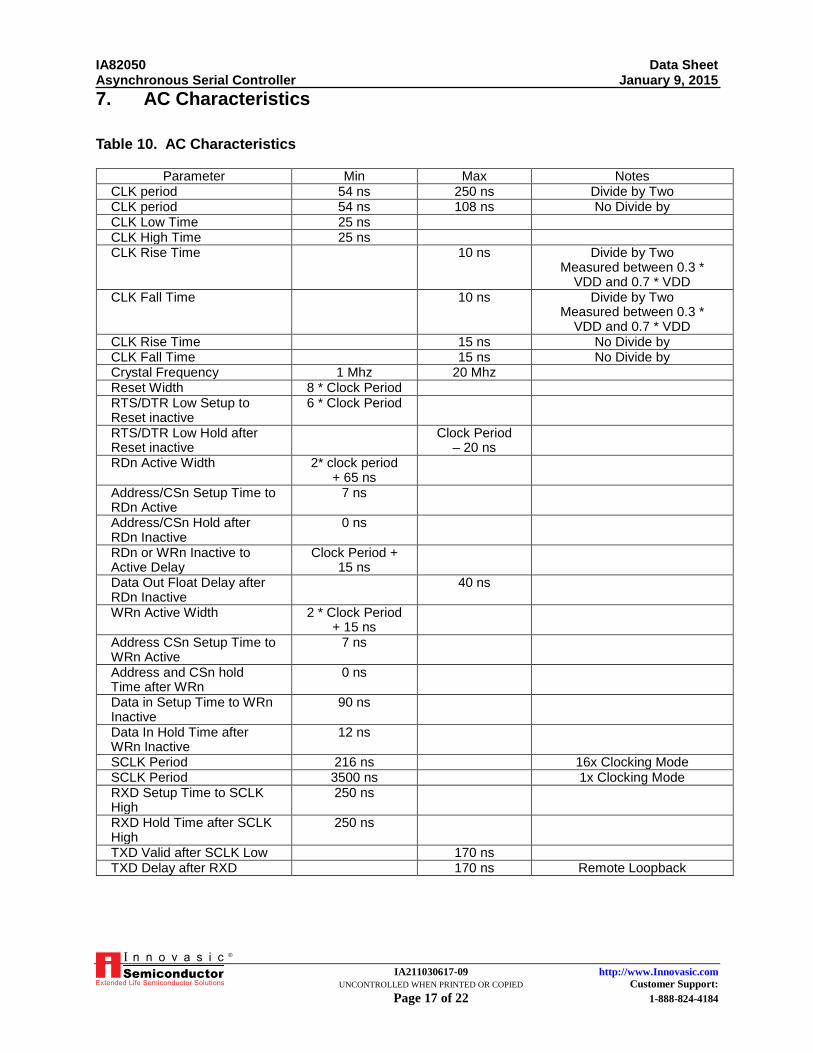
7. AC Characteristics
Table 10. AC Characteristics
Parameter Min Max Notes CLK period 54 ns 250 ns Divide by Two CLK period 54 ns 108 ns No Divide by CLK Low Time 25 ns CLK High Time 25 ns CLK Rise Time 10 ns Divide by Two
Measured between 0.3 * VDD and 0.7 * VDD
CLK Fall Time 10 ns Divide by Two Measured between 0.3 *
VDD and 0.7 * VDD CLK Rise Time 15 ns No Divide by CLK Fall Time 15 ns No Divide by Crystal Frequency 1 Mhz 20 Mhz Reset Width 8 * Clock Period RTS/DTR Low Setup to Reset inactive
6 * Clock Period
RTS/DTR Low Hold after Reset inactive
Clock Period – 20 ns
RDn Active Width 2* clock period + 65 ns
Address/CSn Setup Time to RDn Active
7 ns
Address/CSn Hold after RDn Inactive
0 ns
RDn or WRn Inactive to Active Delay
Clock Period + 15 ns
Data Out Float Delay after RDn Inactive
40 ns
WRn Active Width 2 * Clock Period + 15 ns
Address CSn Setup Time to WRn Active
7 ns
Address and CSn hold Time after WRn
0 ns
Data in Setup Time to WRn Inactive
90 ns
Data In Hold Time after WRn Inactive
12 ns
SCLK Period 216 ns 16x Clocking Mode SCLK Period 3500 ns 1x Clocking Mode RXD Setup Time to SCLK High
250 ns
RXD Hold Time after SCLK High
250 ns
TXD Valid after SCLK Low 170 ns TXD Delay after RXD 170 ns Remote Loopback

IA82050 Data Sheet Asynchronous Serial Controller January 9, 2015
IA211030617-09 http://www.Innovasic.com UNCONTROLLED WHEN PRINTED OR COPIED Customer Support: Page 18 of 22 1-888-824-4184
®
D
L
A1
A
B
B1
e
Side View (Length)
Pin
Identifier
1Pin Count
Direction
E1 E
Top
eA
eBC
Side View (Width)
8. Packaging Information
8.1 PDIP Package
Figure 3. PDW Physical Package Dimensions
Legend:
Symbol
28 (in Inches)
Min Max
A - 0.200
A1 0.015 -
B 0.015 0.020
B1 0.050 0.070
C 0.008 0.012
E 0.580 0.610
E1 0.520 0.560
e 0.100 TYP
eA 0.580 -
eB - 0.686
L 0.100 Min
B2 - -
S - -

IA82050 Data Sheet Asynchronous Serial Controller January 9, 2015
IA211030617-09 http://www.Innovasic.com UNCONTROLLED WHEN PRINTED OR COPIED Customer Support: Page 19 of 22 1-888-824-4184
®
D3
E3
PIN 1
IDENTIFIER & ZONE
1.2
2/1
.07
2 P
LC
S
TOP VIEW
.10
.51 MIN.
R 1.14 / .64
SEATING PLANE
A1
e
.81 / .66
A
.53 / .33
D2 / E2
SIDE VIEW
D
D1
E E1
BOTTOM VIEW
8.2 PLCC Package
Legend:
Symbol
28 (in Millimeters)
Min Max
A 4.20 4.57
A1 2.29 3.04
D1 11.43 11.58
D2 9.91 10.92
D3 7.62 BSC
E1 11.43 11.58
E2 9.91 10.92
E3 7.62 BSC
e 1.27 BSC
D 12.32 12.57
E 12.32 12.57
Figure 4. PLCC Physical Package Dimensions
IA82050 Data Sheet Asynchronous Serial Controller January 9, 2015
IA211030617-09 http://www.Innovasic.com UNCONTROLLED WHEN PRINTED OR COPIED Customer Support: Page 20 of 22 1-888-824-4184
®
9. Innovasic Part Number Cross-Reference
Table 11. Innovasic Part Number Cross-Reference for the PDIP
Innovasic Part Number Intel Part Number Package Type Temperature Grades
IA82050-PDW28I-R-01 lead free (RoHS-compliant)
P82050 TP82050
28-Pin Plastic Dual In-Line Package (PDIP) (600 mils)
Industrial
Table 12. Innovasic Part Number Cross-Reference for the PLCC
Innovasic Part Number Intel Part Number Package Type Temperature Grades
IA82050-PLC28IR2 lead free (RoHS-compliant)
N82050 TN82050
28-Lead Plastic Leaded Chip Carrier (PLCC)
Industrial
IA82050 Data Sheet Asynchronous Serial Controller January 9, 2015
IA211030617-09 http://www.Innovasic.com UNCONTROLLED WHEN PRINTED OR COPIED Customer Support: Page 21 of 22 1-888-824-4184
®
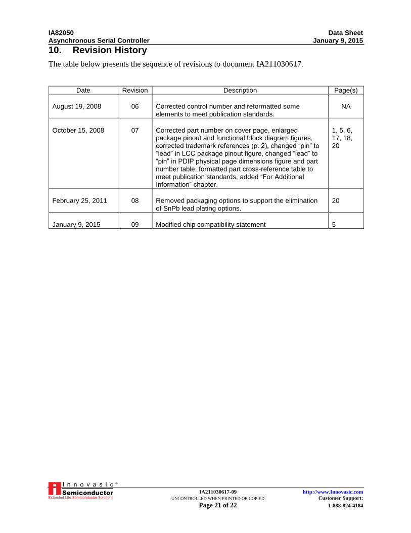
10. Revision History
The table below presents the sequence of revisions to document IA211030617.
Date Revision Description Page(s)
August 19, 2008 06 Corrected control number and reformatted some elements to meet publication standards.
NA
October 15, 2008 07 Corrected part number on cover page, enlarged package pinout and functional block diagram figures, corrected trademark references (p. 2), changed “pin” to “lead” in LCC package pinout figure, changed “lead” to “pin” in PDIP physical page dimensions figure and part number table, formatted part cross-reference table to meet publication standards, added “For Additional Information” chapter.
1, 5, 6, 17, 18, 20
February 25, 2011 08 Removed packaging options to support the elimination of SnPb lead plating options.
20
January 9, 2015 09 Modified chip compatibility statement 5
IA82050 Data Sheet Asynchronous Serial Controller January 9, 2015
IA211030617-09 http://www.Innovasic.com UNCONTROLLED WHEN PRINTED OR COPIED Customer Support: Page 22 of 22 1-888-824-4184
®
11. For Additional Information
The IA82050 is a "plug-and-play" drop-in replacement for the original IC. This data sheet
documents all necessary engineering information about the IA82050 including functional and
I/O descriptions, electrical characteristics and applicable timing.
The Innovasic Support Team wants our information to be complete, accurate, useful, and easy to
understand. Please feel free to contact our experts at Innovasic at any time with suggestions,
comments, or questions.
Innovasic Support Team
3737 Princeton NE
Suite 130
Albuquerque, NM 87107
(505) 883-5263
Fax: (505) 883-5477
Toll Free: (888) 824-4184
E-mail: [email protected]
Website: www.Innovasic.com