cmos scc serial communications controller product...
TRANSCRIPT
Z80C30/Z85C30
CMOS SCC Serial Communications Controller
Cop
Product Specification
PS011705-0608
yright ©2008 by Zilog®, Inc. All rights reserved.www.Zilog.com

CMOS SCC Serial Communications ControllerProduct Specification
ii
DO NOT USE IN LIFE SUPPORT
LIFE SUPPORT POLICYZilog'S PRODUCTS ARE NOT AUTHORIZED FOR USE AS CRITICAL COMPONENTS IN LIFESUPPORT DEVICES OR SYSTEMS WITHOUT THE EXPRESS PRIOR WRITTEN APPROVAL OFTHE PRESIDENT AND GENERAL COUNSEL OF Zilog CORPORATION.
As used hereinLife support devices or systems are devices which (a) are intended for surgical implant into the body, or (b)support or sustain life and whose failure to perform when properly used in accordance with instructions foruse provided in the labeling can be reasonably expected to result in a significant injury to the user. Acritical component is any component in a life support device or system whose failure to perform can bereasonably expected to cause the failure of the life support device or system or to affect its safety oreffectiveness.
Document Disclaimer©2008 by Zilog, Inc. All rights reserved. Information in this publication concerning the devices,applications, or technology described is intended to suggest possible uses and may be superseded. Zilog,INC. DOES NOT ASSUME LIABILITY FOR OR PROVIDE A REPRESENTATION OF ACCURACYOF THE INFORMATION, DEVICES, OR TECHNOLOGY DESCRIBED IN THIS DOCUMENT. ZilogALSO DOES NOT ASSUME LIABILITY FOR INTELLECTUAL PROPERTY INFRINGEMENTRELATED IN ANY MANNER TO USE OF INFORMATION, DEVICES, OR TECHNOLOGYDESCRIBED HEREIN OR OTHERWISE. The information contained within this document has beenverified according to the general principles of electrical and mechanical engineering.
Z8, Z8 Encore!, Z8 Encore! XP, Z8 Encore! MC, Crimzon, eZ80, and ZNEO are trademarks or registeredtrademarks of Zilog, Inc. All other product or service names are the property of their respective owners.
Warning:
PS011705-0608
CMOS SCC Serial Communications ControllerProduct Specification
iii
Revision HistoryEach instance in Revision History reflects a change to this document from its previous revision. For more details, refer to the corresponding pages and appropriate links in the table below.
Date Revision Level Description Page No
June2008
05 Updated Zilog logo, Zilog Text, Disclaimer as per latest template.
All
September 2004
01 Original issue All
PS011705-0608 Revision History

PS011705-0608 Table of Contents
CMOS SCC Serial Communications ControllerProduct Specification
iv
Table of ContentsOverview . . . . . . . . . . . . . . . . . . . . . . . . . . . . . . . . . . . . . . . . . . . . . . . . . . . . . . 1
Other Features for Z85C30 Only . . . . . . . . . . . . . . . . . . . . . . . . . . . . . . . . . . . 2
General Description . . . . . . . . . . . . . . . . . . . . . . . . . . . . . . . . . . . . . . . . . . . . . 4Z85C30/Z80C30 Common Pin Functions . . . . . . . . . . . . . . . . . . . . . . . . . . . . 6
Z85C30 . . . . . . . . . . . . . . . . . . . . . . . . . . . . . . . . . . . . . . . . . . . . . . . . . . . . 9Z80C30 . . . . . . . . . . . . . . . . . . . . . . . . . . . . . . . . . . . . . . . . . . . . . . . . . . . . 9
Functional Description . . . . . . . . . . . . . . . . . . . . . . . . . . . . . . . . . . . . . . . . . . 13I/O Interface Capabilities . . . . . . . . . . . . . . . . . . . . . . . . . . . . . . . . . . . . . . . . 14Programming . . . . . . . . . . . . . . . . . . . . . . . . . . . . . . . . . . . . . . . . . . . . . . . . . 27Z85C30 . . . . . . . . . . . . . . . . . . . . . . . . . . . . . . . . . . . . . . . . . . . . . . . . . . . . . 27Z80C30 . . . . . . . . . . . . . . . . . . . . . . . . . . . . . . . . . . . . . . . . . . . . . . . . . . . . . 28Z85C30/Z80C30 Setup . . . . . . . . . . . . . . . . . . . . . . . . . . . . . . . . . . . . . . . . . 28Z85C30 Timing . . . . . . . . . . . . . . . . . . . . . . . . . . . . . . . . . . . . . . . . . . . . . . . 34Z80C30 Timing . . . . . . . . . . . . . . . . . . . . . . . . . . . . . . . . . . . . . . . . . . . . . . . 37
Electrical Characteristics . . . . . . . . . . . . . . . . . . . . . . . . . . . . . . . . . . . . . . . . 41Absolute Maximum Ratings . . . . . . . . . . . . . . . . . . . . . . . . . . . . . . . . . . . . . . 41Standard Test Conditions . . . . . . . . . . . . . . . . . . . . . . . . . . . . . . . . . . . . . . . 41Capacitance . . . . . . . . . . . . . . . . . . . . . . . . . . . . . . . . . . . . . . . . . . . . . . . . . 42Miscellaneous . . . . . . . . . . . . . . . . . . . . . . . . . . . . . . . . . . . . . . . . . . . . . . . . 43DC Characteristics . . . . . . . . . . . . . . . . . . . . . . . . . . . . . . . . . . . . . . . . . . . . 43Z80C30/Z85C30 . . . . . . . . . . . . . . . . . . . . . . . . . . . . . . . . . . . . . . . . . . . . . . 43AC Characteristics . . . . . . . . . . . . . . . . . . . . . . . . . . . . . . . . . . . . . . . . . . . . . 44Z85C30 Read/Write Timing Diagrams . . . . . . . . . . . . . . . . . . . . . . . . . . . . . 44
Packaging . . . . . . . . . . . . . . . . . . . . . . . . . . . . . . . . . . . . . . . . . . . . . . . . . . . . 63Part Number Suffix Designations . . . . . . . . . . . . . . . . . . . . . . . . . . . . . . . . . 66
Customer Support . . . . . . . . . . . . . . . . . . . . . . . . . . . . . . . . . . . . . . . . . . . . . . 67
CMOS SCC Serial Communications ControllerProduct Specification
1
OverviewThe features of Zilog’s Z80C30 and Z85C30 devices include:
• Z85C30 — Optimized for Non-Multiplexed Bus Microprocessors.
• Z80C30 — Optimized for Multiplexed Bus Microprocessors.
• Pin Compatible to NMOS Versions.
• Two Independent, 0 to 4.1 Mbit/Second, Full-Duplex Channels. Each channel withSeparate Crystal Oscillator, Baud Rate Generator (BRG), and Digital Phase-LockedLoop (DPLL) for Clock Recovery.
• Multi-Protocol Operation under Program Control; Programmable for NRZ, NRZI, orFM Data Encoding.
• Asynchronous Mode with Five to Eight Bits and One, One and One-Half, or TwoStop Bits Per Character, Programmable Clock Factor, Break Detection and Generation; Parity, Overrun, and Framing Error Detection.
• Synchronous Mode with Internal or External Character Synchronization on One orTwo Synchronous Characters and CRC Generation and Checking with CRC-16 orCRC-CCITT Preset to either 1s or 0s.
• SDLC/HDLC Mode with Comprehensive Frame-Level Control, Automatic Zero Insertion and Deletion, I-Field Residue Handling, Abort Generation and Detection,CRC Generation and Checking, and SDLC Loop.
• Software Interrupt Acknowledge Feature (not available with NMOS).
• Local Loopback and Auto Echo Modes.
• Supports T1 Digital Trunk.
• Enhanced DMA Support (not available with NMOS) 10 x 19-Bit Status FIFO 14-BitByte Counter.
• Speeds:– Z85C3O — 8.5, 10, 16.384 MHz– Z80C3O — 8, 10 MHz
PS011705-0608 Overview

CMOS SCC Serial Communications ControllerProduct Specification
2
Other Features for Z85C30 OnlySome of the features listed below are available by default. Some of them (features with *) are disabled on default to maintain compatibility with the existing Serial Communications Controller (SCC) design, and “program to enable through WR7”:
• New programmable WR7 (Write register 7 prime) to enable new features.
• Improvements to support SDLC mode of synchronous communication:– Improve functionality to ease sending back-to-back frames.– Automatic SDLC opening Flag transmission.*– Automatic Tx Underrun/EOM Latch reset in SDLC mode.*– Automatic RTS deactivation.*– TxD pin forced High in SDLC NRZI mode after closing flag.*– Complete CRC reception.*– Improved response to Abort sequence in status FIFO.– Automatic Tx CRC generator preset/reset.– Extended Read for Write registers.*– Write data set-up timing improvement.
• Improved AC timing:– 3 to 3.6 PCLK access recovery time.– Programmable DTR/REQ timing.*– Write data to falling edge of WR setup time requirement is now eliminated.– Reduced INT timing.
• Other features include:– Extended Read function to read back the written value to the Write registers.*– Latching RRO during read.– RRO, bit D7 and RR10, bit D6 now has reset default value.
PS011705-0608 Overview
CMOS SCC Serial Communications ControllerProduct Specification
3
PS011705-0608 Overview
CMOS SCC Serial Communications ControllerProduct Specification
4
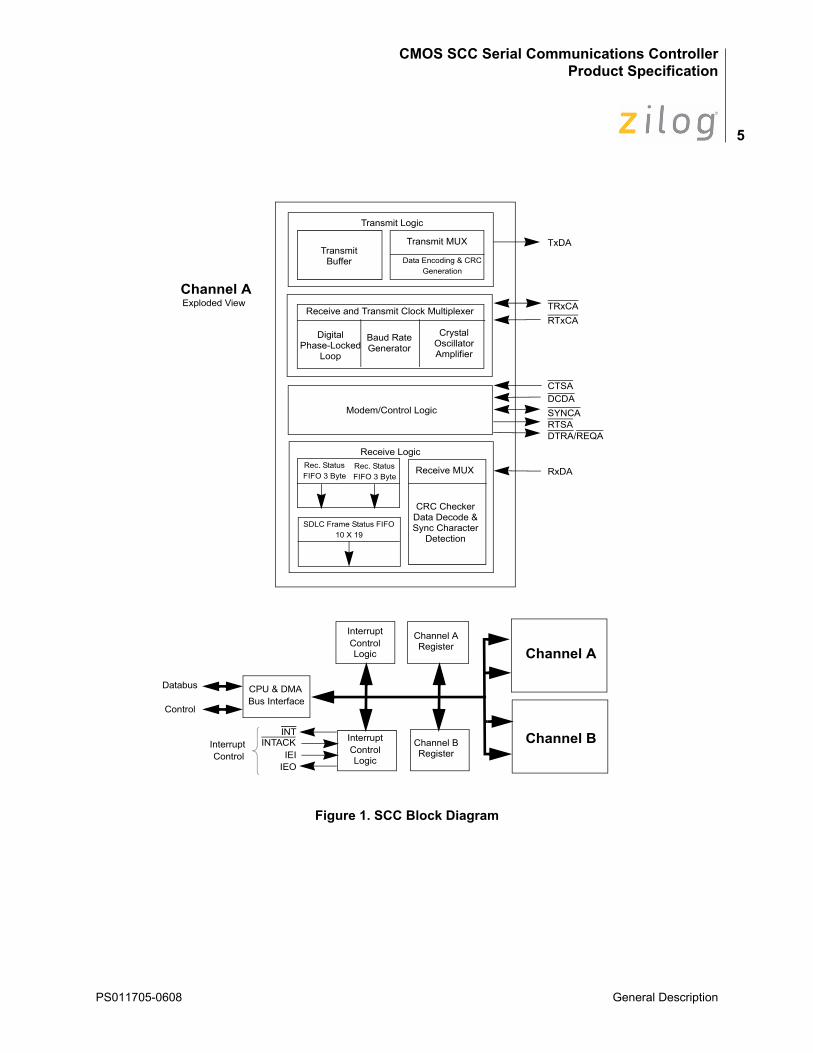
General DescriptionThe Z80C30/Z85C30 Serial Communications Controller (SCC), is a pin and software compatible CMOS member of the SCC family introduced by Zilog® in 1981. It is a dual channel, multi-protocol data communications peripheral that easily interfaces with CPU’s with either multiplexed or non-multiplexed address/data buses. The advanced CMOS process offers lower power consumption, higher performance, and superior noise immunity. The programming flexibility of the internal registers allow the SCC to be configured to various serial communications applications.Figure 1 displays a block diagram of the SCC.The many on-chip features such as Baud Rate Generators (BRG), Digital Phase Locked Loops (DPLL), and crystal oscillators reduce the need for an external logic. Additional features include a 10 x 19-bit status FIFO and 14-bit byte counter to support high speed SDLC transfers using DMA controllers.The SCC handles asynchronous formats, synchronous byte-oriented protocols such as IBM Bisync, and synchronous bit-oriented protocols such as HDLC and IBM SDLC. This device supports virtually any serial data transfer application (for example, cassette, diskette, tape drives, etc.).The device generates and checks CRC codes in any synchronous mode and can be programmed to check data integrity in various modes. The SCC also contains facilities for modem controls in both channels. In applications where these controls are not required, the modem controls can be used for general-purpose I/O. The daisy-chain interrupt hierar-chy is also supported.
PS011705-0608 General Description
CMOS SCC Serial Communications ControllerProduct Specification
5
Figure 1. SCC Block Diagram
Channel AExploded View
Databus
ControlInterrupt
IEIIEO
INTACKINT
Control
CPU & DMABus Interface
ControlInterrupt
Logic
ControlInterrupt
Logic
Channel BRegister
Channel ARegister
RxDA
Channel A
Channel B
Receive Logic
Receive MUX
CRC CheckerData Decode &Sync Character
Detection
Rec. StatusFIFO 3 Byte
Rec. StatusFIFO 3 Byte
SDLC Frame Status FIFO10 X 19
CTSADCDASYNCARTSADTRA/REQA
Modem/Control Logic
DigitalPhase-Locked
Loop
Baud RateGenerator
CrystalOscillatorAmplifier
Receive and Transmit Clock Multiplexer
TransmitBuffer
Transmit Logic
Transmit MUX
Data Encoding & CRCGeneration
TxDA
TRxCARTxCA
PS011705-0608 General Description

CMOS SCC Serial Communications ControllerProduct Specification
6
Pin DescriptionsZ85C30/Z80C30 Common Pin Functions
The following sections describe the pin functions common to Z85C30 and Z80C30 devices:
• CTSA, CTSB
• DCDA, DCDB
• DTR/REQA, DTR/REQB
• IEI
• IEO
• INT
• INTACK
• PCLK
• RxDA, RxDB
• RTxCA, RTxCB
• RTSA, RTSB
• SYNCA, SYNCB
• TxDA, TxDB
• TRxCA, TRxCB
• W/REQA, W/REQBEach pin function is described below.
CTSA, CTSBClear To Send (inputs, active Low) — If these pins are programmed for Auto Enable, a Low on the inputs enables the respective transmitters. If not programmed as Auto Enable, these pins can be used as general-purpose inputs. Both inputs are Schmitt-trigger buffered to accommodate slow rise-time inputs. The SCC detects pulses on these inputs and can interrupt the CPU on both logic level transitions.
DCDA, DCDBData Carrier Detect (inputs, active Low) — These pins function as receiver enables if programmed for Auto Enable. Otherwise, these pins are used as general-purpose input pins. Both pins are Schmitt-trigger buffered to accommodate slow rise-time signals. The SCC detects pulses on these pins and can interrupt the CPU on both logic leveltransitions.
PS011705-0608 General Description
CMOS SCC Serial Communications ControllerProduct Specification
7
DTR/REQA, DTR/REQBData Terminal Ready/Request (outputs, active Low) — These outputs follow the state programmed into the DTR bit. They can also be used as general-purpose outputs or as Request lines for a DMA controller.
IEIInterrupt Enable In (input, active High) — IEI is used with IEO to form an interrupt daisy-chain when there is more than one interrupt driven device. A high IEI indicates that no other higher priority device has an interrupt under service or is requesting an interrupt.
IEOInterrupt Enable Out (output, active High) — IEO is High only if IEI is High and the CPU is not servicing the SCC interrupt or the SCC is not requesting an interrupt (interrupt Acknowledge cycle only). IEO is connected to the next lower priority device’s IEI input and thus inhibits interrupts from lower priority devices.
INTInterrupt Request (output, open-drain, active Low) — This signal activates when the SCC requests an interrupt.
INTACKInterrupt Acknowledge (input, active Low) — This signal indicates an active Interrupt Acknowledge cycle. During this cycle, the SCC interrupt daisy chain settles. When RD is active, the SCC places an interrupt vector on the data bus (if IEI is High). INTACK is latched by the rising edge of PCLK.
PCLKClock (input) — This is the master SCC clock used to synchronize internal signals. PCLK is a TTL level signal. PCLK is not required to have any phase relationship with the master system clock. The maximum transmit rate is 1/4 PCLK.
RxDA, RxDBReceive Data (inputs, active High) — These signals receive serial data at standard TTL levels.
RTxCA, RTxCBReceive/Transmit Clocks (inputs, active Low) — These pins can be programmed in several different operating modes. In each channel, RTxC can supply the receive clock, the transmit clock, clock for the Baud Rate Generator, or the clock for the Digital Phase-Locked Loop. These pins can also be programmed for use with the respective SYNC pins as a crystal oscillator. The receive clock can be 1, 16, 32, or 64 times the data rate in Asyn-chronous modes.
PS011705-0608 General Description
CMOS SCC Serial Communications ControllerProduct Specification
8
RTSA, RTSBRequest To Send (outputs, active Low) — When the Request To Send (RTS) bit in Write Register 5 (see Figure 9 on page 19) is set, the RTS signal goes Low. When the RTS bit is reset in the Asynchronous mode and Auto Enable is ON, the signal goes High after the transmitter is empty. In Synchronous mode, it strictly follows the state of the RTS bit. When Auto Enable is OFF, the RTS pins can be used as general-purpose outputs.
SYNCA, SYNCBSynchronization (inputs or outputs, active Low) — These pins function as inputs, outputs, or part of the crystal oscillator circuit. In the Asynchronous Receive mode (crystal oscillator option not selected), these pins are inputs similar to CTS and DCD. In this mode, transitions on these lines affect the state of the Synchronous/Hunt status bits in Read Register 0 (see Figure 8 on page 17) but have no other function.In External Synchronization mode with the crystal oscillator not selected, these lines also act as inputs. In this mode, SYNC must be driven Low for two receive clock cycles after the last bit in the synchronous character is received. Character assembly begins on the rising edge of the receive clock immediately preceding the activation of SYNC.In the Internal Synchronization mode (Monosync and Bisync) with the crystal oscillator not selected, these pins act as outputs and are active only during the part of the receive clock cycle in which synchronous characters are recognized. This synchronous condition is not latched. These outputs are active each time a synchronization pattern is recognized (regardless of character boundaries). In SDLC mode, these pins act as outputs and are valid on receipt of a flag.
TxDA, TxDBTransmit Data (outputs, active High) — These output signals transmit serial data at standard TTL levels.
TRxCA, TRxCBTransmit/Receive Clocks (inputs or outputs, active Low) — These pins can be programmed in several different operating modes. TRxC may supply the receive clock or the transmit clock in the input mode or supply the output of the Digital Phase-locked loop, the crystal oscillator, the Baud Rate Generator, or the transmit clock in the output mode.
W/REQA, W/REQBWait/Request (outputs, open-drain when programmed for a Wait function, driven High or low when programmed for a Request function) — These dual-purpose outputs can be programmed as Request lines for a DMA controller or as Wait lines to synchronize the CPU to the SCC data rate. The reset state is Wait.
PS011705-0608 General Description
CMOS SCC Serial Communications ControllerProduct Specification
9
Z85C30
A/BChannel A/Channel B (input) — This signal selects the channel in which the Read or Write operation occurs.
CEChip Enable (input, active Low) — This signal selects the SCC for a Read or Writeoperation.
D7–D0Data Bus (bidirectional, tri-state) — These lines carry data and command to and from the SCC.
D/CData/Control Select (input) — This signal defines the type of information transferred to or from the SCC. A High indicates a data transfer; a Low indicates a command.
RDRead (input, active Low) — This signal indicates a Read operation and when the SCC is selected, enables the SCC’s bus drivers. During the Interrupt Acknowledge cycle, this signal gates the interrupt vector onto the bus if the SCC is the highest priority device requesting an interrupt.
WRWrite (input, active Low) — When the SCC is selected, this signal indicates a Write operation. The coincidence of RD and WR is interpreted as a reset.
Z80C30
AD7–AD0Address/Data Bus (bidirectional, active High, Tri-state) — These multiplexed lines carry register addresses to the SCC as well as data or control information.
ASAddress Strobe (input, active Low) — Addresses on AD7–AD0 are latched by the rising edge of this signal.
CS0Chip Select 0 (input, active Low) — This signal is latched concurrently with the addresses on AD7–AD0 and must be active for the intended bus transaction to occur.
PS011705-0608 General Description
CMOS SCC Serial Communications ControllerProduct Specification
10
CS1Chip Select 1 (input, active High) — This second select signal must also be active before the intended bus transaction can occur. CS1 must remain active throughout the transaction.
DSData strobe (input, active Low) — This signal provides timing for the transfer of data into and out of the SCC. If AS and DS coincide, this confluence is interpreted as a reset.
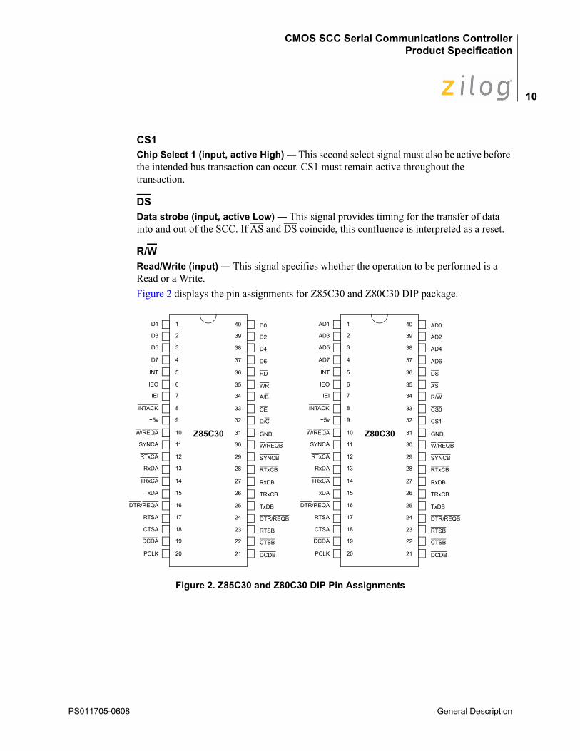
R/WRead/Write (input) — This signal specifies whether the operation to be performed is a Read or a Write.Figure 2 displays the pin assignments for Z85C30 and Z80C30 DIP package.
Figure 2. Z85C30 and Z80C30 DIP Pin Assignments
D1
D3
D5
D7
INT
IEO
IEI
INTACK
+5v
W/REQA
SYNCA
RTxCA
RxDA
TRxCA
TxDA
DTR/REQA
RTSA
CTSA
DCDA
PCLK
D0
D2
D4
D6
RD
WR
A/B
CE
D/C
GND
W/REQB
SYNCB
RTxCB
RxDB
TRxCB
TxDB
DTR/REQB
RTSB
CTSB
DCDB
40
39
38
37
36
35
34
33
32
31
30
29
28
27
26
25
24
23
22
21
1
2
3
4
5
6
7
8
9
10
11
12
13
14
15
16
17
18
19
20
Z85C30
AD1
AD3
AD5
AD7
INT
IEO
IEI
INTACK
+5v
W/REQA
SYNCA
RTxCA
RxDA
TRxCA
TxDA
DTR/REQA
RTSA
CTSA
DCDA
PCLK
AD0
AD2
AD4
AD6
DS
AS
R/W
CS0
CS1
GND
W/REQB
SYNCB
RTxCB
RxDB
TRxCB
TxDB
DTR/REQB
RTSB
CTSB
DCDB
40
39
38
37
36
35
34
33
32
31
30
29
28
27
26
25
24
23
22
21
1
2
3
4
5
6
7
8
9
10
11
12
13
14
15
16
17
18
19
20
Z80C30
PS011705-0608 General Description
CMOS SCC Serial Communications ControllerProduct Specification
11
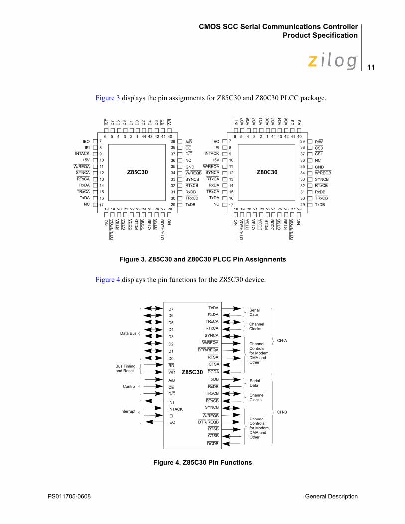
Figure 3 displays the pin assignments for Z85C30 and Z80C30 PLCC package.
Figure 3. Z85C30 and Z80C30 PLCC Pin Assignments
Figure 4 displays the pin functions for the Z85C30 device.
Figure 4. Z85C30 Pin Functions
IEO
Z85C30
IEIINTACK
+5V
W/REQASYNCARTxCA
RxDATRxCA
TxDANC
A/BCED/CNC
GNDW/REQBSYNCBRTxCBRxDBTRxCBTxDB
INT
D7
D5
D3
D1
D0
D2
D4
D6
RD
WR
NC
DTR
/RE
QA
RTS
AC
TSA
DC
DA
PCLD
DC
DB
CTS
BR
TSB
DTR
/RE
QB
NC
78910111213141516
17
38373635343332313029
396 5 4 3 2 1 44 43 42 41 40
18 19 20 21 22 23 24 25 26 27 28
IEO
Z80C30
IEIINTACK
+5V
W/REQASYNCARTxCA
RxDATRxCA
TxDANC
R/WCS0CS1NC
GNDW/REQBSYNCBRTxCBRxDBTRxCBTxDB
INT
AD
7A
D5
AD
3
AD
1A
D0
AD
2A
D4
AD
6D
S
AS
NC
DTR
/RE
QA
RTS
AC
TSA
DC
DA
PCLK
DC
DB
CTS
BR
TSB
DTR
/RE
QB
NC
78910111213141516
17
38373635343332313029
396 5 4 3 2 1 44 43 42 41 40
18 19 20 21 22 23 24 25 26 27 28
Z85C30
SerialData
ChannelClocks
CH-AChannelControlsfor Modem,DMA andOther
CH-B
SerialData
ChannelClocks
ChannelControlsfor Modem,DMA andOther
Data Bus
D7
D6
D5
D4
D3
D2
D1
D0
RDWR
A/B
CED/C
INT
INTACK
IEI
IEO
TxDA
RxDA
TRxCA
RTxCA
SYNCA
W/REQA
DTR/REQA
RTSA
CTSA
DCDA
TxDB
RTxCBSYNCB
W/REQB
DTR/REQB
RTSB
CTSB
DCDB
RxDB
TRxCB
and Reset
Control
Interrupt
Bus Timing
PS011705-0608 General Description
CMOS SCC Serial Communications ControllerProduct Specification
12
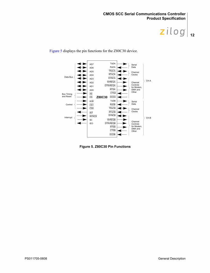
Figure 5 displays the pin functions for the Z80C30 device.
Figure 5. Z80C30 Pin Functions
Z80C30
SerialData
ChannelClocks
CH-AChannelControlsfor Modem,DMA andOther
CH-B
SerialData
ChannelClocks
ChannelControlsfor Modem,DMA andOther
Data Bus
AD7
AD6
AD5
AD4
AD3
AD2
AD1
AD0
ASDS
R/W
CS1CS0
INT
INTACK
IEI
IEO
TxDA
RxDA
TRxCA
RTxCA
SYNCA
W/REQA
DTR/REQA
RTSA
CTSA
DCDA
TxDB
RTxCBSYNCB
W/REQB
DTR/REQB
RTSB
CTSB
DCDB
RxDB
TRxCB
and Reset
Control
Interrupt
Bus Timing
PS011705-0608 General Description
CMOS SCC Serial Communications ControllerProduct Specification
13
Functional DescriptionThe architecture of the SCC is described below:
• As a data communications device which transmits and receives data in various protocols.
• As a microprocessor peripheral in which the SCC offers valuable featuressuch as vectored interrupts and DMA support.
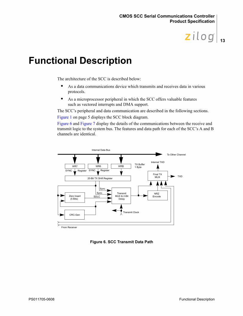
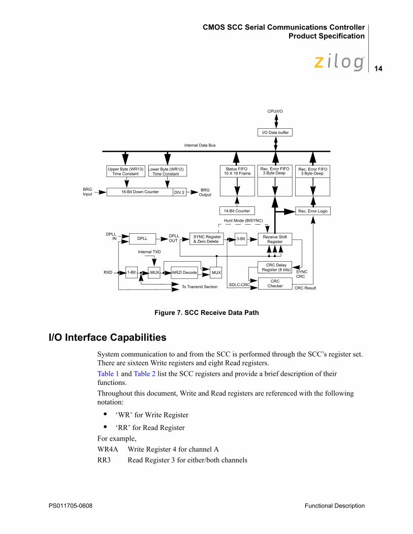
The SCC’s peripheral and data communication are described in the following sections.Figure 1 on page 5 displays the SCC block diagram. Figure 6 and Figure 7 display the details of the communications between the receive and transmit logic to the system bus. The features and data path for each of the SCC’s A and B channels are identical.
Figure 6. SCC Transmit Data Path
From Receiver
CRC-Gen
Zero Insert(5 Bits)
20-Bit TX Shift Register
SYNC Register SYNC Register
Internal Data Bus
To Other Channel
Internal TXD
TXD
NRZEncode
TransmitMUX & 2-Bit
Delay
Transmit Clock
TX Buffer1 Byte
Final TXMUX
WRBWR6
Sync
SyncSDLC
WR7
PS011705-0608 Functional Description
CMOS SCC Serial Communications ControllerProduct Specification
14
Figure 7. SCC Receive Data Path
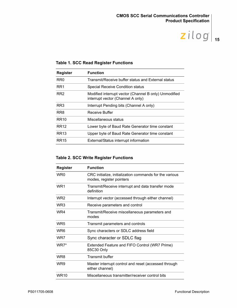
I/O Interface CapabilitiesSystem communication to and from the SCC is performed through the SCC’s register set. There are sixteen Write registers and eight Read registers. Table 1 and Table 2 list the SCC registers and provide a brief description of their functions.Throughout this document, Write and Read registers are referenced with the following notation:
• ‘WR’ for Write Register
• ‘RR’ for Read RegisterFor example,WR4A Write Register 4 for channel ARR3 Read Register 3 for either/both channels
To Transmit Section
MUXNRZI DecodeMUX
Internal TXD
DPLL SYNC Register& Zero DeleteOUT
SDLC-CRCCRC
Checker CRC Result
SYNCCRC
CRC DelayRegister (8 bits)
Receive ShiftRegister
3-Bit
RXD
DPLLIN DPLL
1-Bit
Hunt Mode (BISYNC)
14-Bit Counter Rec. Error Logic
BRGOutput
Rec. Error FIFO3 Byte Deep
Rec. Error FIFO3 Byte Deep
Status FIFO10 X 19 Frame
I/O Data buffer
Internal Data Bus
CPU/I/O
BRGInput 16-Bit Down Counter DIV 2
Upper Byte (WR13)Time Constant
Lower Byte (WR12)Time Constant
PS011705-0608 Functional Description
CMOS SCC Serial Communications ControllerProduct Specification
15
Table 1. SCC Read Register Functions
Register Function
RR0 Transmit/Receive buffer status and External status
RR1 Special Receive Condition status
RR2 Modified interrupt vector (Channel B only) Unmodified interrupt vector (Channel A only)
RR3 Interrupt Pending bits (Channel A only)
RR8 Receive Buffer
RR10 Miscellaneous status
RR12 Lower byte of Baud Rate Generator time constant
RR13 Upper byte of Baud Rate Generator time constant
RR15 External/Status interrupt information
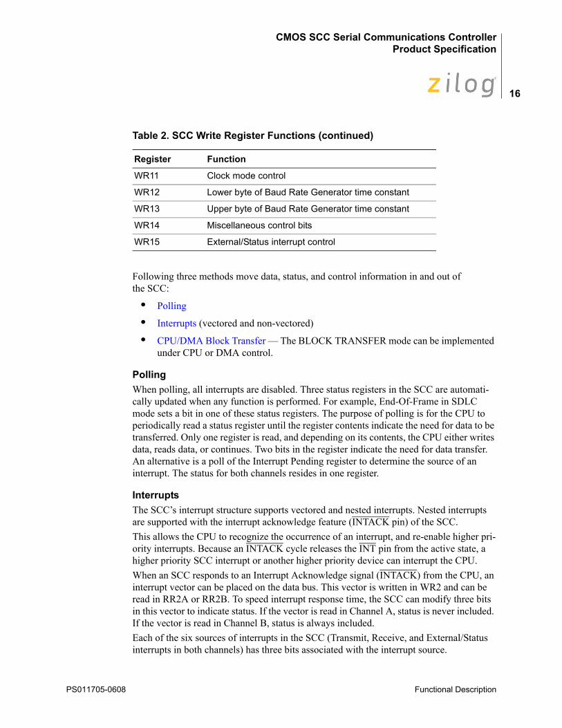
Table 2. SCC Write Register Functions
Register Function
WR0 CRC initialize, initialization commands for the various modes, register pointers
WR1 Transmit/Receive interrupt and data transfer mode definition
WR2 Interrupt vector (accessed through either channel)
WR3 Receive parameters and control
WR4 Transmit/Receive miscellaneous parameters and modes
WR5 Transmit parameters and controls
WR6 Sync characters or SDLC address field
WR7 Sync character or SDLC flag
WR7* Extended Feature and FIFO Control (WR7 Prime) 85C30 Only
WR8 Transmit buffer
WR9 Master interrupt control and reset (accessed through either channel)
WR10 Miscellaneous transmitter/receiver control bits
PS011705-0608 Functional Description
CMOS SCC Serial Communications ControllerProduct Specification
16
Following three methods move data, status, and control information in and out of the SCC:
• Polling
• Interrupts (vectored and non-vectored)
• CPU/DMA Block Transfer — The BLOCK TRANSFER mode can be implemented under CPU or DMA control.
PollingWhen polling, all interrupts are disabled. Three status registers in the SCC are automati-cally updated when any function is performed. For example, End-Of-Frame in SDLC mode sets a bit in one of these status registers. The purpose of polling is for the CPU to periodically read a status register until the register contents indicate the need for data to be transferred. Only one register is read, and depending on its contents, the CPU either writes data, reads data, or continues. Two bits in the register indicate the need for data transfer. An alternative is a poll of the Interrupt Pending register to determine the source of an interrupt. The status for both channels resides in one register.
InterruptsThe SCC’s interrupt structure supports vectored and nested interrupts. Nested interrupts are supported with the interrupt acknowledge feature (INTACK pin) of the SCC. This allows the CPU to recognize the occurrence of an interrupt, and re-enable higher pri-ority interrupts. Because an INTACK cycle releases the INT pin from the active state, a higher priority SCC interrupt or another higher priority device can interrupt the CPU. When an SCC responds to an Interrupt Acknowledge signal (INTACK) from the CPU, an interrupt vector can be placed on the data bus. This vector is written in WR2 and can be read in RR2A or RR2B. To speed interrupt response time, the SCC can modify three bits in this vector to indicate status. If the vector is read in Channel A, status is never included. If the vector is read in Channel B, status is always included.Each of the six sources of interrupts in the SCC (Transmit, Receive, and External/Status interrupts in both channels) has three bits associated with the interrupt source.
WR11 Clock mode control
WR12 Lower byte of Baud Rate Generator time constant
WR13 Upper byte of Baud Rate Generator time constant
WR14 Miscellaneous control bits
WR15 External/Status interrupt control
Table 2. SCC Write Register Functions (continued)
Register Function
PS011705-0608 Functional Description
CMOS SCC Serial Communications ControllerProduct Specification
17
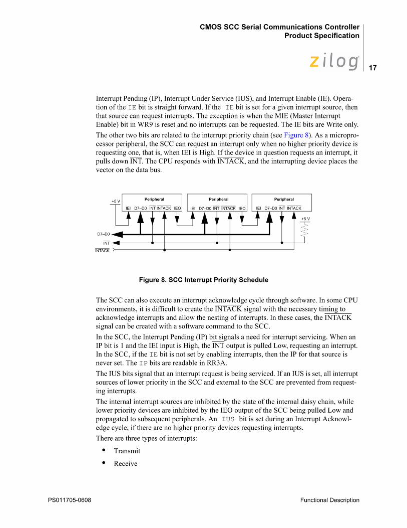
Interrupt Pending (IP), Interrupt Under Service (IUS), and Interrupt Enable (IE). Opera-tion of the IE bit is straight forward. If the IE bit is set for a given interrupt source, then that source can request interrupts. The exception is when the MIE (Master Interrupt Enable) bit in WR9 is reset and no interrupts can be requested. The IE bits are Write only.The other two bits are related to the interrupt priority chain (see Figure 8). As a micropro-cessor peripheral, the SCC can request an interrupt only when no higher priority device is requesting one, that is, when IEI is High. If the device in question requests an interrupt, it pulls down INT. The CPU responds with INTACK, and the interrupting device places the vector on the data bus.
Figure 8. SCC Interrupt Priority Schedule
The SCC can also execute an interrupt acknowledge cycle through software. In some CPU environments, it is difficult to create the INTACK signal with the necessary timing to acknowledge interrupts and allow the nesting of interrupts. In these cases, the INTACK signal can be created with a software command to the SCC.In the SCC, the Interrupt Pending (IP) bit signals a need for interrupt servicing. When an IP bit is 1 and the IEI input is High, the INT output is pulled Low, requesting an interrupt. In the SCC, if the IE bit is not set by enabling interrupts, then the IP for that source is never set. The IP bits are readable in RR3A.The IUS bits signal that an interrupt request is being serviced. If an IUS is set, all interrupt sources of lower priority in the SCC and external to the SCC are prevented from request-ing interrupts. The internal interrupt sources are inhibited by the state of the internal daisy chain, while lower priority devices are inhibited by the IEO output of the SCC being pulled Low and propagated to subsequent peripherals. An IUS bit is set during an Interrupt Acknowl-edge cycle, if there are no higher priority devices requesting interrupts.There are three types of interrupts:
• Transmit
• Receive
+5 V
+5 V
D7–D0
INT
INTACK
IEI D7–D0 INT INTACK IEO IEI D7–D0 INT INTACK IEO IEI D7–D0 INT INTACK
Peripheral PeripheralPeripheral
PS011705-0608 Functional Description
CMOS SCC Serial Communications ControllerProduct Specification
18
• External/StatusEach interrupt type is enabled under program control with Channel A having higher priority than Channel B, and with Receiver, Transmit, and External/Status interrupts prioritized in that order within each channel.When enabled, the receiver interrupts the CPU in one of three ways:
• Interrupt on First Receive Character or Special Receive Condition
• Interrupt on All Receive Characters or Special Receive Conditions
• Interrupt on Special Receive Conditions OnlyInterrupt on First Character or Special Condition and Interrupt on Special Condition Only are typically used with the Block Transfer mode. A special Receive Condition is one of the following. receiver overrun, framing error in Asynchronous mode, end-of-frame in SDLC mode and, optionally, a parity error. The Special Receive Condition interrupt is different from an ordinary receive character available interrupt only by the status placed in the vec-tor during the Interrupt Acknowledge cycle. In Interrupt on First Receive Character, an interrupt occurs from Special Receive Conditions anytime after the first receive character interrupt.The main function of the External/Status interrupt is to monitor the signal transitions of the CTS, DCD, and SYNC pins, however, an External/Status interrupt is also caused by a Transmit Underrun condition; a zero count in the Baud Rate Generator; by the detection of a Break (Asynchronous mode), Abort (SDLC mode) or EOP (SDLC Loop mode) sequence in the data stream. The interrupt caused by the Abort or EOP has a special fea-ture allowing the SCC to interrupt when the Abort or EOP sequence is detected or termi-nated. This feature facilitates the proper termination of the current message, correct initialization of the next message, and the accurate timing of the Abort condition in exter-nal logic in SDLC mode. In SDLC Loop mode, this feature allows secondary stations to recognize the primary station regaining control of the loop during a poll sequence.
Software Interrupt AcknowledgeOn the CMOS version of the SCC, the SCC interrupt acknowledge cycle can be initiated through software. If Write Register 9 (WR9) bit D5 is set, Read Register 2 (RR2) results in an interrupt acknowledge cycle to be executed internally. Like a hardware INTACK cycle, a software acknowledge causes the INT pin to return High, the IEO pin to go low and set the IUS latch for the highest priority interrupt pending.Similar to using the hardware INTACK signal, a software acknowledge cycle requires that a Reset Highest IUS command be issued in the interrupt service routine. Whenever an interrupt acknowledge cycle is used, hardware or software, a reset highest IUS command is required. If RR2 is read from channel A, the unmodified vector is returned. If RR2 is read from channel B, then the vector is modified to indicate the source of the interrupt. The Vector Includes Status (VIS) and No Vector (NV) bits in WR9 are ignored when bit 05 is set to 1.
PS011705-0608 Functional Description
CMOS SCC Serial Communications ControllerProduct Specification
19
When the INTACK and IEI pins are not being used, they should be pulled up to VCC through a resistor (10 KΩ typical).
CPU/DMA Block TransferThe SCC provides a Block Transfer mode to accommodate CPU block transfer functions and DMA controllers. The Block Transfer mode uses the WAIT/REOUEST output in con-junction with the Wait/Request bits in WR1. The WAIT/REOUEST output can be defined under software control as a WAIT line in the CPU Block Transfer mode or as a REQUEST line in the DMA Block Transfer mode.To a DMA controller, the SCC REQUEST output indicates that the SCC is ready to trans-fer data to or from memory To the CPU, the WAIT line indicates that the ESCC is not ready to transfer data, thereby requesting that the CPU extend the I/O cycle. The DTR/REQUEST line allows full-duplex operation under DMA control.
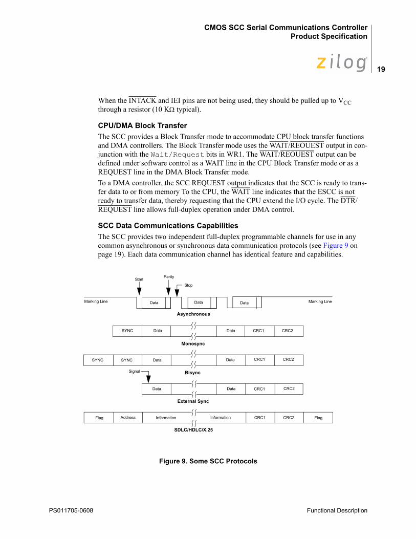
SCC Data Communications CapabilitiesThe SCC provides two independent full-duplex programmable channels for use in any common asynchronous or synchronous data communication protocols (see Figure 9 on page 19). Each data communication channel has identical feature and capabilities.
Figure 9. Some SCC Protocols
Flag Address Information CRC1 CRC2Information Flag
Data
SYNC
CRC1
Signal
CRC1 CRC2
Marking Line
Data CRC2
SYNC Data Data
CRC1 CRC2SYNC Data Data
Start
SDLC/HDLC/X.25
Parity
Stop
Data Data Data Marking Line
External Sync
Bisync
Monosync
Asynchronous
PS011705-0608 Functional Description
CMOS SCC Serial Communications ControllerProduct Specification
20
Asynchronous ModesSend and Receive is accomplished independently on each channel with five to eight bits per character, plus optional even or odd parity. The transmitters can supply one, one-and-a-half, or two stop bits per character and can provide a break output at any time. The receiver break-detection logic interrupts the CPU both at the start and at the end of a received break. Reception is protected from spikes by a transient spike-rejection mechanism that checks the signal one-half a bit time after a Low level is detected on the receive data input (RxDA or RxDB pins). If the Low does not persist (a transient), the character assembly process does not start.Framing errors and overrun errors are detected and buffered together with the partial char-acter on which they occur. Vectored interrupts allow fast servicing or error conditions using dedicated routines. A built-in checking process avoids the interpretation of a fram-ing error as a new start bit. A framing error results in the addition of one-half a bit time to the point at which the search for the next start bit begins.The SCC does not require symmetric transmit and receive clock signals - a feature allow-ing use of the wide variety of clock sources. The transmitter and receiver handle data at a rate supplied to the receive and transmit clock inputs. In Asynchronous modes, the SYNC pin can be programmed as an input used for functions such as monitoring a ring indicator.
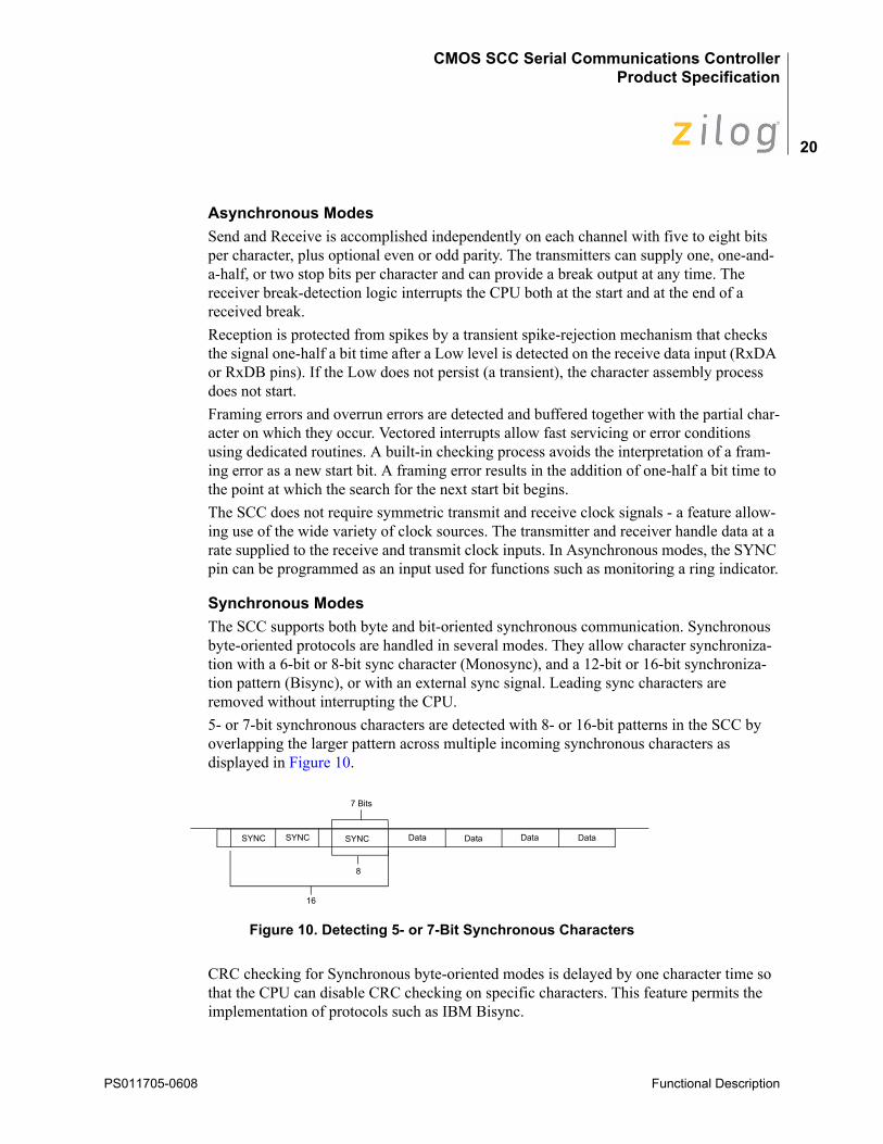
Synchronous ModesThe SCC supports both byte and bit-oriented synchronous communication. Synchronous byte-oriented protocols are handled in several modes. They allow character synchroniza-tion with a 6-bit or 8-bit sync character (Monosync), and a 12-bit or 16-bit synchroniza-tion pattern (Bisync), or with an external sync signal. Leading sync characters are removed without interrupting the CPU.5- or 7-bit synchronous characters are detected with 8- or 16-bit patterns in the SCC by overlapping the larger pattern across multiple incoming synchronous characters asdisplayed in Figure 10.
Figure 10. Detecting 5- or 7-Bit Synchronous Characters
CRC checking for Synchronous byte-oriented modes is delayed by one character time so that the CPU can disable CRC checking on specific characters. This feature permits the implementation of protocols such as IBM Bisync.
Data Data DataDataSYNC SYNC
7 Bits
8
16
SYNC
PS011705-0608 Functional Description
CMOS SCC Serial Communications ControllerProduct Specification
21
Both CRC-16 (X16 + X15 + X12 +1) and CCITT (X16 + X12 + X5 + 1) error-checking polynomials are supported. Either polynomial can be selected in all Synchronous modes. You can preset the CRC generator and checker to all 1’s or all 0’s. The SCC also provides a feature that automatically transmits CRC data when no other data is available for trans-mission. This feature allows for high speed transmissions under DMA control, with no need for CPU intervention at the end of a message. When there is no data or CRC to send in Synchronous modes, the transmitter inserts 6-,8-, or 16-bit sync characters, regardless of the programmed character length.
SDLC ModeThe SCC supports Synchronous bit-oriented protocols, such as SDLC and HDLC, byperforming automatic flag sending, zero insertion, and CRC generation. A special command is used to abort a frame in transmission. At the end of a message, the SCC auto-matically transmits the CRC and trailing flag when the transmitter underruns. The trans-mitter can also be programmed to send an idle line consisting of continuous flag characters or a steady marking condition.If a transmit underrun occurs in the middle of a message, an external/status interrupt warns the CPU of this status change, issuing an abort. The SCC can also be programmed to send an abort itself in case of an underrun, relieving the CPU of this task. One to eight bits per character can be sent, allowing reception of a message with no prior information about the character structure in the information field of a frame.The receiver automatically acquires synchronization on the leading flag of a frame in SDLC or HDLC and provides a synchronization signal on the SYNC pin (an interrupt can also be programmed). The receiver can be programmed to search for frames addressed by a single byte (or four bits within a byte) of a user-selected address or to a global broadcast address. In this mode, frames not matching either the user-selected or broadcast address are ignored.The number of address bytes are extended under software control. For receiving data, an interrupt on the first received character, or an interrupt on every character, or on special condition only (end-of-frame) can be selected. The receiver automatically deletes all 0’s inserted by the transmitter during character assembly CRC is also calculated and is auto-matically checked to validate frame transmission. At the end of transmission, the status of a received frame is available in the status registers. In SDLC mode, the SCC must be pro-grammed to use the SDLC CRC polynomial, but the generator and checker can be preset to all 1’s or all 0’s. The CRC inverts before transmission and the receiver checks against the bit pattern 0001110100001111.NRZ, NRZI or FM coding can be used in any 1 x mode. The parity options available in Asynchronous modes are available in Synchronous modes.
SDLC Loop ModeThe SCC supports SDLC Loop mode in addition to normal SDLC. In an SDLC Loop, a primary controller station manages the message traffic flow on the loop and any number of secondary stations. In SDLC Loop mode, the SCC performs the functions of a secondary
PS011705-0608 Functional Description
CMOS SCC Serial Communications ControllerProduct Specification
22
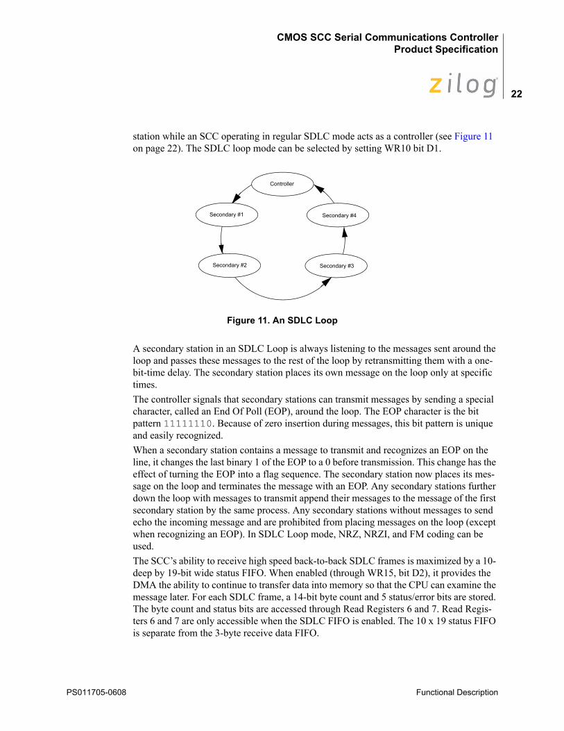
station while an SCC operating in regular SDLC mode acts as a controller (see Figure 11 on page 22). The SDLC loop mode can be selected by setting WR10 bit D1.
Figure 11. An SDLC Loop
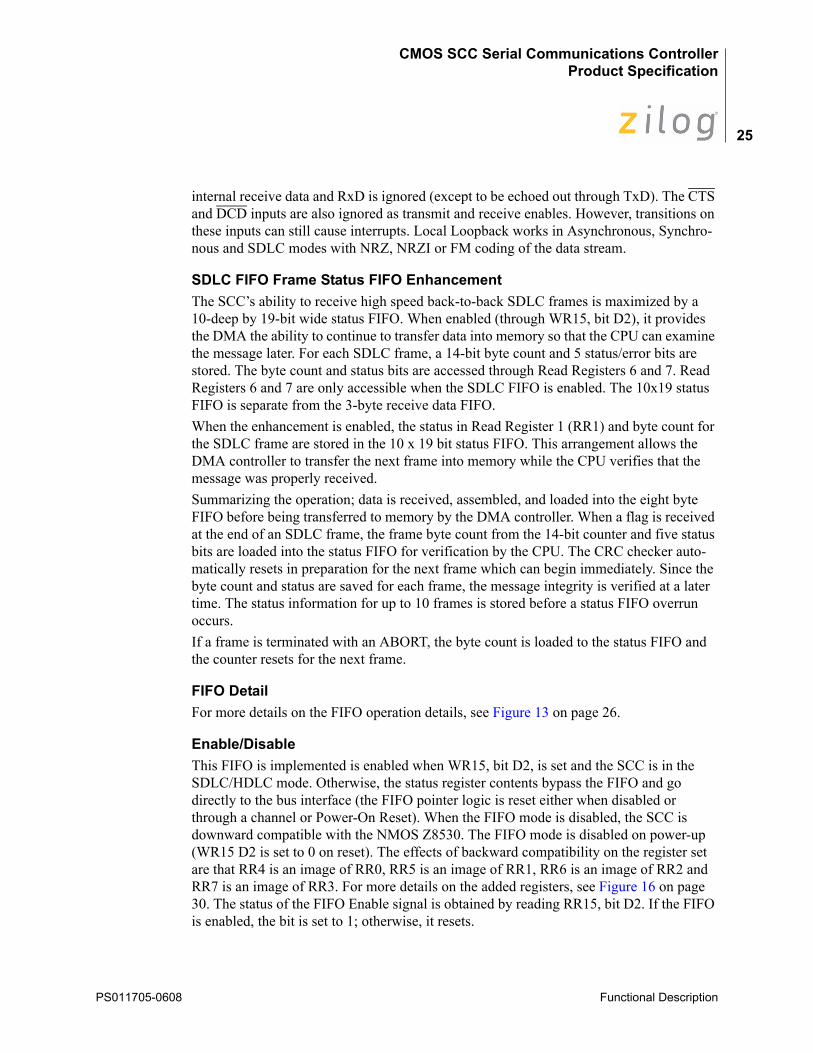
A secondary station in an SDLC Loop is always listening to the messages sent around the loop and passes these messages to the rest of the loop by retransmitting them with a one-bit-time delay. The secondary station places its own message on the loop only at specific times. The controller signals that secondary stations can transmit messages by sending a special character, called an End Of Poll (EOP), around the loop. The EOP character is the bit pattern 11111110. Because of zero insertion during messages, this bit pattern is unique and easily recognized.When a secondary station contains a message to transmit and recognizes an EOP on the line, it changes the last binary 1 of the EOP to a 0 before transmission. This change has the effect of turning the EOP into a flag sequence. The secondary station now places its mes-sage on the loop and terminates the message with an EOP. Any secondary stations further down the loop with messages to transmit append their messages to the message of the first secondary station by the same process. Any secondary stations without messages to send echo the incoming message and are prohibited from placing messages on the loop (except when recognizing an EOP). In SDLC Loop mode, NRZ, NRZI, and FM coding can be used.The SCC’s ability to receive high speed back-to-back SDLC frames is maximized by a 10- deep by 19-bit wide status FIFO. When enabled (through WR15, bit D2), it provides the DMA the ability to continue to transfer data into memory so that the CPU can examine the message later. For each SDLC frame, a 14-bit byte count and 5 status/error bits are stored. The byte count and status bits are accessed through Read Registers 6 and 7. Read Regis-ters 6 and 7 are only accessible when the SDLC FIFO is enabled. The 10 x 19 status FIFO is separate from the 3-byte receive data FIFO.
Secondary #2 Secondary #3
Secondary #4
Controller
Secondary #1
PS011705-0608 Functional Description
CMOS SCC Serial Communications ControllerProduct Specification
23
Baud Rate GeneratorEach channel in the SCC contains a programmable Baud Rate Generator (BRG). Each generator consists of two 8-bit time constant registers that form a 16-bit time constant, a 16-bit down counter, and a flip-flop on the output producing a square wave. On startup, the output flip-flop is set in a High state, the value in the time constant register is loaded into the counter, and the counter starts counting down. The output of the BRG toggles when reaching 0, the value in the time constant register is loaded into the counter, and the process is repeated. The time constant can be changed at any time, but the new value does not take effect until the next load of the counter.The output of the BRG can be used as either the transmit clock, the receive clock, or both. It can also drive the Digital Phase-locked loop (see Digital Phase-Locked Loop).If the receive clock or transmit clock is not programmed to come from the TRxC pin, the output of the BRG can be echoed out through the TRxC pin. The following formula relates the time constant to the baud rate where PCLK or RTxC is the BRG input frequency in Hertz. The clock mode is 1, 16, 32, or 64, as selected in Write Register 4, bits D6 and D7. Synchronous operation modes select 1 and Asynchronous modes select 16, 32 or 64.
Digital Phase-Locked LoopThe SCC contains a Digital Phase-Locked Loop (DPLL) to recover clock information from a data stream with NRZI or FM encoding. The DPLL is driven by a clock that is nominally 32 (NRZI) or 16 (FM) times the data rate. The DPLL uses this clock, along with the data stream, to construct a clock for the data. This clock is used as the SCC receive clock, the transmit clock, or both. When the DPLL is selected as the transmit clock source, it provides a jitter-free clock output that is the DPLL input frequency divided by the appropriate divisor for the selected encoding technique.For NRZI encoding, the DPLL counts the 32x clock to create nominal bit times. As the 32x clock is counted, the DPLL is searching the incoming data stream for edges (either 1 to 0, or 0 to 1). Whenever an edge is detected, the DPLL makes a count adjustment (during the next counting cycle), producing a terminal count closer to the center of the bit cell.For FM encoding, the DPLL again counts from 0 to 31, but with a cycle corresponding to two bit times. When the DPLL is locked, the clock edges in the data stream occur between counts 15 and 16 and between counts 31 and 0. The DPLL looks for edges only during a time centered on the 15 to 16 counting transition.The 32x clock for the DPLL can be programmed to come from either the RTxC input or the output of the BRG. The DPLL output can be programmed to be echoed out of the SCC through the TRxC pin (if this pin is not being used as an input).
Time Constant =PCLK or RTxC Frequency
2(Baud Rate)(Clock Mode)-2
PS011705-0608 Functional Description
CMOS SCC Serial Communications ControllerProduct Specification
24
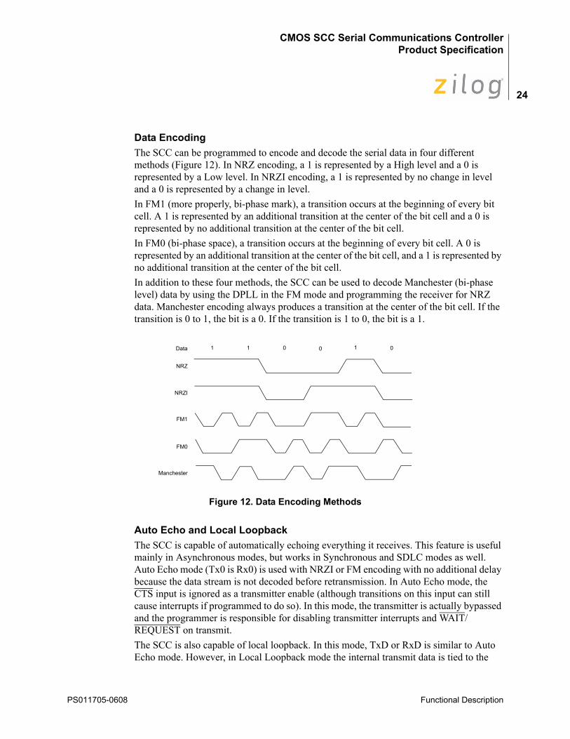
Data EncodingThe SCC can be programmed to encode and decode the serial data in four different methods (Figure 12). In NRZ encoding, a 1 is represented by a High level and a 0 is represented by a Low level. In NRZI encoding, a 1 is represented by no change in level and a 0 is represented by a change in level. In FM1 (more properly, bi-phase mark), a transition occurs at the beginning of every bit cell. A 1 is represented by an additional transition at the center of the bit cell and a 0 isrepresented by no additional transition at the center of the bit cell. In FM0 (bi-phase space), a transition occurs at the beginning of every bit cell. A 0 isrepresented by an additional transition at the center of the bit cell, and a 1 is represented by no additional transition at the center of the bit cell. In addition to these four methods, the SCC can be used to decode Manchester (bi-phase level) data by using the DPLL in the FM mode and programming the receiver for NRZ data. Manchester encoding always produces a transition at the center of the bit cell. If the transition is 0 to 1, the bit is a 0. If the transition is 1 to 0, the bit is a 1.
Figure 12. Data Encoding Methods
Auto Echo and Local LoopbackThe SCC is capable of automatically echoing everything it receives. This feature is useful mainly in Asynchronous modes, but works in Synchronous and SDLC modes as well. Auto Echo mode (Tx0 is Rx0) is used with NRZI or FM encoding with no additional delay because the data stream is not decoded before retransmission. In Auto Echo mode, the CTS input is ignored as a transmitter enable (although transitions on this input can still cause interrupts if programmed to do so). In this mode, the transmitter is actually bypassed and the programmer is responsible for disabling transmitter interrupts and WAIT/REQUEST on transmit.The SCC is also capable of local loopback. In this mode, TxD or RxD is similar to Auto Echo mode. However, in Local Loopback mode the internal transmit data is tied to the
Data
NRZ
NRZI
FM1
FM0
Manchester
1 1 0 00 1
PS011705-0608 Functional Description
CMOS SCC Serial Communications ControllerProduct Specification
25
internal receive data and RxD is ignored (except to be echoed out through TxD). The CTS and DCD inputs are also ignored as transmit and receive enables. However, transitions on these inputs can still cause interrupts. Local Loopback works in Asynchronous, Synchro-nous and SDLC modes with NRZ, NRZI or FM coding of the data stream.
SDLC FIFO Frame Status FIFO EnhancementThe SCC’s ability to receive high speed back-to-back SDLC frames is maximized by a 10-deep by 19-bit wide status FIFO. When enabled (through WR15, bit D2), it provides the DMA the ability to continue to transfer data into memory so that the CPU can examine the message later. For each SDLC frame, a 14-bit byte count and 5 status/error bits are stored. The byte count and status bits are accessed through Read Registers 6 and 7. Read Registers 6 and 7 are only accessible when the SDLC FIFO is enabled. The 10x19 status FIFO is separate from the 3-byte receive data FIFO.When the enhancement is enabled, the status in Read Register 1 (RR1) and byte count for the SDLC frame are stored in the 10 x 19 bit status FIFO. This arrangement allows the DMA controller to transfer the next frame into memory while the CPU verifies that the message was properly received.Summarizing the operation; data is received, assembled, and loaded into the eight byte FIFO before being transferred to memory by the DMA controller. When a flag is received at the end of an SDLC frame, the frame byte count from the 14-bit counter and five status bits are loaded into the status FIFO for verification by the CPU. The CRC checker auto-matically resets in preparation for the next frame which can begin immediately. Since the byte count and status are saved for each frame, the message integrity is verified at a later time. The status information for up to 10 frames is stored before a status FIFO overrun occurs.If a frame is terminated with an ABORT, the byte count is loaded to the status FIFO and the counter resets for the next frame.
FIFO DetailFor more details on the FIFO operation details, see Figure 13 on page 26.
Enable/DisableThis FIFO is implemented is enabled when WR15, bit D2, is set and the SCC is in the SDLC/HDLC mode. Otherwise, the status register contents bypass the FIFO and go directly to the bus interface (the FIFO pointer logic is reset either when disabled or through a channel or Power-On Reset). When the FIFO mode is disabled, the SCC is downward compatible with the NMOS Z8530. The FIFO mode is disabled on power-up (WR15 D2 is set to 0 on reset). The effects of backward compatibility on the register set are that RR4 is an image of RR0, RR5 is an image of RR1, RR6 is an image of RR2 and RR7 is an image of RR3. For more details on the added registers, see Figure 16 on page 30. The status of the FIFO Enable signal is obtained by reading RR15, bit D2. If the FIFO is enabled, the bit is set to 1; otherwise, it resets.
PS011705-0608 Functional Description
CMOS SCC Serial Communications ControllerProduct Specification
26
Read OperationWhen WR15 bit D2 sets and the FIFO is not empty, the next read to status register RR1 or registers RR7 and RR6, is from the FIFO. Reading status register RR1 causes one location of the FIFO to become empty. Status is read after reading the byte count, otherwise the count is incorrect. Before the FIFO underflows, it is disabled. In this case, the multiplexer is switched allowing status to read directly from the status register. Reads from RR7 and RR6 contain bits that are undefined. Bit D6 of RR7 (FIFO Data Available) determines if status data is coming from the FIFO or directly from the status register, which sets to 1 when the FIFO is not empty. Not all status bits are stored in the FIFO. The All Sent, Parity, and EOF bits bypass the FIFO. Status bits sent through the FIFO are Residue Bits (3), Overrun, and CRC Error.
Figure 13. SDLC Frame Status FIFO
Over Equal
Reset on Flag Detect
Increment on Byte Detection
Enable Count in SDLC
End of Frame SignalStatus Read Comp
Tail Pointer4-Bit Counter
Head Pointer4-Bit Counter
4-Bit Comparator
14 Bits
Byte Counter
Frame Status FIFO Circuitry
5 Bits
FIFO Array10 Deep by 19 Bits Wide
SCC Status RegResidue Bits (3)
Overrun, CRC ErrorRR1
5 Bits
EN
6 Bits 8 Bits
6-Bit MUX
2 Bits
EOF = 1
6 BitsRR1
Bit 7 Bit 6 Bits 5-0 RR6FIFO Enable
RR7 D5-D0 + RR6 D7-D0Byte Counter Contains 14 bitsfor a 16 KByte maximum count
RR7 D6FIFO Data available status bit Status Bit set to 1When reading from FIFO
RR7 D7FIFO Overflow Status BitMSB pf RR(7) is set on Status FIFO overflow
WR(15) Bit 2Set EnablesStatus FIFO
In SDLC Mode the following definitions apply
– All Sent bypasses MUX and equals contents of SCC Status Register– Parity Bits bypasses MUX and does the same– EOF is set to 1 whenever reading from the FIFO
Interfaceto SCC
PS011705-0608 Functional Description
CMOS SCC Serial Communications ControllerProduct Specification
27
The sequence for operation of the byte count and FIFO logic is to read the registers in the following order. RR7, RR6, and RR1 (reading RR6 is optional). Additional logic prevents the FIFO from being emptied by multiple reads from RR1. The read from RR7 latches the FIFO empty/full status bit (D6) and steers the status multiplexer to read from the SCC megacell instead of the status FIFO (since the status FIFO is empty). The read from RR1 allows an entry to be read from the FIFO (if the FIFO was empty, logic was added to prevent a FIFO underflow condition).
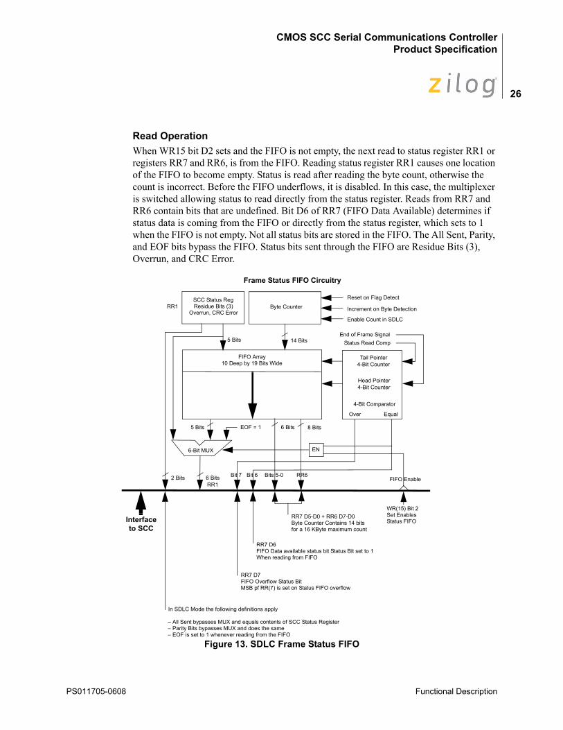
Write OperationWhen the end of an SDLC frame (EOF) is received and the FIFO is enabled, the contents of the status and byte-count registers are loaded into the FIFO. The EOF signal is used to increment the FIFO. If the FIFO overflows, RR7, bit D7 (FIFO Overflow) sets to indicate the overflow. This bit and the FIFO control logic is reset by disabling and re-enabling the FIFO control bit (WR15, bit 02). For details of FIFO control timing during an SDLC frame, see Figure 14.
Figure 14. SDLC Byte Counting Detail
ProgrammingThe SCC contains Write registers in each channel that are programmed by the system separately to configure the functional personality of the channels.
Z85C30In the SCC, the data registers are directly addressed by selecting a High on the D/C pin. With all other registers (except WR0 and RR0), programming the Write registers requires two Write operations and reading the read registers requires both a Write and a Read oper-ation. The first write is to WR0 and contains three bits that point to the selected register. The second write is the actual control word for the selected register, and if the second operation is read, the selected Read register is accessed. All the SCC registers, including the data registers, can be accessed in this fashion. The pointer bits are automatically cleared after the Read or Write operation so that WR0 (or RR0) is addressed again.
Don’t LoadCounter On 1st FlagReset ByteCounter Here
ResetByte CounterLoad CounterInto FIFO andIncrement PTR
Internal Byte StrobeIncrements Counter
ResetByte Counter
Internal Byte StrobeIncrements Counter
ResetByte CounterLoad CounterInto FIFO andIncrement PTR
F A D D D D C C F
0 7 0
F A D D D D C C F
0 7 0
PS011705-0608 Functional Description
CMOS SCC Serial Communications ControllerProduct Specification
28
Z80C30All SCC registers are directly addressable. A command issued in WR0B controls how the SCC decodes the address placed on the address/data bus at the beginning of a Read or Write cycle. In the Shift Right mode, the channel select A/B is taken from AD0 and the state of AD5 is ignored. In the Shift Left mode, the channel select A/B is taken from AD5 and the state of AD0 is ignored. AD7 and AD6 are always ignored as address bits and the register address occupies AD4-AD1.
Z85C30/Z80C30 Setup
InitializationThe system program first issues a series of commands to initialize the basic mode of operation. This is followed by other commands to qualify conditions within the selected mode. For example, in the Asynchronous mode, character length, clock rate, number of stop bits, and even or odd parity must be set first. The interrupt mode is set, and finally, the receiver and transmitter are enabled.
Write RegistersThe SCC contains 15 Write registers for the 80C30, while there are 16 for the 85C30 (one more additional Write register if counting the transmit buffer) in each channel. These Write registers are programmed separately to configure the functional ‘personality’ of the channels. There are two registers (WR2 and WR9) shared by the two channels that are accessed through either of them. WR2 contains the interrupt vector for both channels, while WR9 contains the interrupt control bits and reset commands. Figure 15 through Figure 18 display the format of each Write register.
PS011705-0608 Functional Description
CMOS SCC Serial Communications ControllerProduct Specification
29
Figure 15. Write Register Bit Functions
Register 0
*
0 00 11 01 1
0 00 11 01 1
Null CodeNull Code
Null CodeNull Code
Null Code
* B Channel Only
Reset Rx CRC CheckerReset Tx CRC CheckerReset Tx Underrun/EOM Latch
Reset Ext/Status InterruptsSend AbortEnable Int on Next Rx CharacterReset Tx Int PendingError ResetReset Highest IUS
Select Shift Left ModeSelect Shift Right Mode
00000
01
1
0
00
00
0
0
11
1
111
111
1
D7 D6 D5 D4 D3 D2 D1 D0
Write Register 0 (multiplexed bus mode)
D7 D6 D5 D4 D3 D2 D1 D0
Write Register 0 (non-multiplexed bus mode)
Null Code000 11 01 1
* With Point High Command
Reset Rx CRC CheckerReset Tx CRC GeneratorReset Tx Underrun/EOM Latch
Register 1Register 2Register 3Register 4Register 5Register 6Register 7Register 8Register 9Register 10Register 11Register 12Register 13Register 14Register 15
*
0 0 00 00 00
0 00
0
0 0 00 0
00
00
0
00
111
1
1 1 111
111
1 1
11
11111
11
0 0 00 00 00
0 00
01 1 1
1111
11 1
11
Null CodePoint HighReset Ext/Status InterruptsSend Abort (SDLC)Enable Int on Next Rx CharacterReset Tx Int PendingError ResetReset Highest IUS
D7 D6 D5 D4 D3 D2 D1 D0
Write Register 1
0 00
01
11 1
Ext Int EnableTx Int EnableParity is Special Condition
Rx Int on Special Condition OnlyInt on all Rx Characters or Special ConditionRx Int on First Character or Special Condition
WAIT/DMA Request onReceive /Transmit
Rx Int Disable
WAIT/DMA Request FunctionWAIT/DMA Request
D7 D6 D5 D4 D3 D2 D1 D0
Write Register 2
V0V1V2V3V4V5V6
V7
InterruptVector
D7 D6 D5 D4 D3 D2 D1 D0
Write Register 3
Rx EnableSync Character Load InhibitAddress Search Mode (SDLC)Rx CRC EnableEnter Hunt ModeAuto Enables
000
01
111
Rx 5 Bits/CharacterRx 7 Bits/CharacterRx 6 Bits/CharacterRx 8 Bits/Character
PS011705-0608 Functional Description
CMOS SCC Serial Communications ControllerProduct Specification
30
Figure 16. Write Register Bit Functions
D7 D6 D5 D4 D3 D2 D1 D0
Write Register 4
Parity Enable
Parity EVEN/ODD
0
000 111 1
0
000 111 1
0
000 111 1
Sync Modes Enable1 Stop Bit/Character1 1/2 Stop Bits/Character2 Stop Bits/Character
8-Bit Sync Character16-Bit Sync CharacterSDLC Mode (01111110 Flag)External Sync Mode
X1 Clock ModeX16 Clock ModeX32 Clock ModeX64 Clock Mode
D7 D6 D5 D4 D3 D2 D1 D0
Write Register 5
00
00
1
1
11
Tx CRC Enable
RTS
SDLC/CRC-16
Tx EnableSend Break
DTR
Tx 5 Bits (or Less)/CharacterTx 7 Bits/CharacterTx 6 Bits/CharacterTx 8 Bits/Character
PS011705-0608 Functional Description
CMOS SCC Serial Communications ControllerProduct Specification
31
Figure 17. Write Register Bit Functions
D7 D6 D5 D4 D3 D2 D1 D0
Write Register 6
Sync7Sync1Sync7Sync3
ADR7ADR7
Sync6Sync0Sync6Sync2
ADR6ADR6
Sync5Sync5Sync5Sync1
ADR5ADR5
Sync4Sync4Sync4Sync0
ADR4ADR4
Sync3Sync3Sync3
1
xADR3
Sync2Sync2Sync2
1
xADR2
Sync1Sync1Sync1
1
xADR1
Sync0Sync0Sync0
1
xADR0
Monosync, 8 BitsMonosync, 6 BitsBisync, 16 BitsBisync, 12 BitsSDLCSDLC (Address Range)
D7 D6 D5 D4 D3 D2 D1 D0
Write Register 7
Sync7Sync5Sync15Sync11
Monosync, 8 BitsMonosync, 6 BitsBisync, 16 BitsBisync, 12 BitsSDLC0
Sync6Sync4Sync14Sync10
1
Sync5Sync3Sync13Sync9
1
Sync4Sync2Sync12Sync8
1
Sync3Sync1Sync11Sync7
1
Sync2Sync0Sync10Sync6
1
Sync1x
Sync9Sync5
1
Sync0x
Sync8Sync4
0
D7 D6 D5 D4 D3 D2 D1 D0
WR 7’ Prime (85C30 only)
Auto Tx Flag
Auto EOM ResetAuto RTS Deactivation
Force TxD HighDTR/REQ Fast ModeComplete CRC ReceptionExtended Read Enable
Reserved (Program as 0)
PS011705-0608 Functional Description
CMOS SCC Serial Communications ControllerProduct Specification
32
Figure 18. Write Register Bit Functions
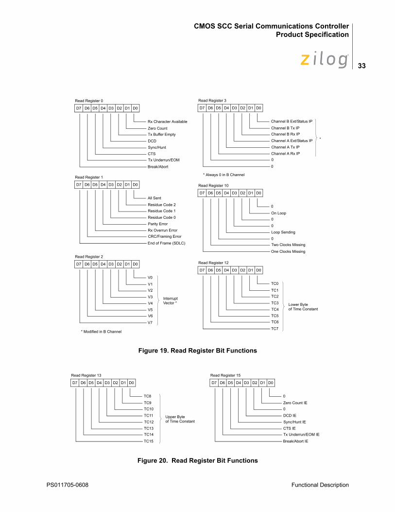
Read RegistersThe SCC contains ten Read registers (eleven, counting the receive buffer (RR8) in each channel). Four of these can be read to obtain status information (RR0, RR1, RR10, and RR15). Two registers (RR12 and RR13) are read to learn the Baud Rate Generator time constant. RR2 contains either the unmodified interrupt vector (Channel A) or the vector modified by status information (Channel B). RR3 contains the Interrupt Pending (IP) bits (Channel A only – Figure 19). RR6 and RR7 contain the information in the SDLC Frame Status FIFO, but is only read when WR15 D2 is set (see Figure 19 and Figure 20).
0
000 111 1
D7 D6 D5 D4 D3 D2 D1 D0
Write Register 9
No ResetChannel Reset BChannel Reset AForce Hardware Reset
VIS
NV
DLC
MIE
Status High/Status Low
Software INTACK Enable
D7 D6 D5 D4 D3 D2 D1 D0
Write Register 10
0
000 111 1
NRZNRZIFM1 (Transition = 1)FM1 (Transition = 0)
CRC Preset I/O
Go Active on Poll
Mark/Flag Idle
Abort/Flag on Underrun
Loop Mode
6-Bit/8-Bit Sync
D7 D6 D5 D4 D3 D2 D1 D0
Write Register 11
0
000 111 1
0
000 111 1
0
000 111 1
TRxC Out = Xtal OutputTRxC Out = Transmit ClockTRxC Out = BR Generator OutputTRxC Out = DPLL Output
TRxC O/I
Transmit Clock = RTxC PinTransmit Clock = TRxC PinTransmit Clock = BR Generator OutputTransmit Clock = DPLL Output
Receive Clock = RTxC PinReceive Clock = TRxC PinReceive Clock = BR Generator OutputReceive Clock = DPLL Output
RTxC Xtal/No Xtal
D7 D6 D5 D4 D3 D2 D1 D0
Write Register 12
TC0
TC1TC2
TC3
TC4
TC5TC6
TC7
Lower Byte ofTime Constant
Upper Byte ofTime Constant
D7 D6 D5 D4 D3 D2 D1 D0
Write Register 13
TC8
TC9TC10
TC11
TC12
TC13TC14
TC15
D7 D6 D5 D4 D3 D2 D1 D0
Write Register 14
BR Generator Enable
BR Generator Source
DTR/Request Function
Auto Echo
Local Loopback
0000
01
1
0
00
00
0
0
11
1
111
111
1
Null CommandEnter Search ModeReset Missing ClockDisable DPLLSet Source = BR GeneratorSet Source = RTxCSet FM ModeSet NRZI Mode
D7 D6 D5 D4 D3 D2 D1 D0
Write Register 15
0
Zero Count IE
SDLC FIFO Enable
DCD IE
Sync/Hunt IE
CTS IE
Tx Underrun/EOM IE
Break/Abort IE
PS011705-0608 Functional Description
CMOS SCC Serial Communications ControllerProduct Specification
33
Figure 19. Read Register Bit Functions
Figure 20. Read Register Bit Functions
D7 D6 D5 D4 D3 D2 D1 D0
Read Register 0
Rx Character Available
Zero CountTx Buffer Empty
DCDSync/HuntCTSTx Underrun/EOM
Break/Abort
D7 D6 D5 D4 D3 D2 D1 D0
Read Register 1
All Sent
Residue Code 2Residue Code 1
Residue Code 0Parity ErrorRx Overrun ErrorCRC/Framing Error
End of Frame (SDLC)
D7 D6 D5 D4 D3 D2 D1 D0
Read Register 2
V0
V1V2
V3V4V5V6
V7
InterruptVector *
* Modified in B Channel
D7 D6 D5 D4 D3 D2 D1 D0
Read Register 12
TC0
TC1TC2
TC3TC4TC5TC6
TC7
Lower Byteof Time Constant
D7 D6 D5 D4 D3 D2 D1 D0
Read Register 10
0
On Loop0
0Loop Sending0Two Clocks Missing
One Clocks Missing
D7 D6 D5 D4 D3 D2 D1 D0
Read Register 3
Channel B Ext/Status IP
Channel B Tx IPChannel B Rx IP
Channel A Ext/Status IPChannel A Tx IPChannel A Rx IP0
0
*
* Always 0 in B Channel
D7 D6 D5 D4 D3 D2 D1 D0
Read Register 13
TC8
TC9TC10
TC11TC12TC13TC14
TC15
Upper Byteof Time Constant
D7 D6 D5 D4 D3 D2 D1 D0
Read Register 15
0
Zero Count IE0
DCD IESync/Hunt IECTS IETx Underrun/EOM IE
Break/Abort IE
PS011705-0608 Functional Description
CMOS SCC Serial Communications ControllerProduct Specification
34
Z85C30 TimingThe SCC generates internal control signals from the WR and RD that are related to PCLK. PCLK has no phase relationship with WR and RD, the circuitry generating the internal control signals provides time for meta-stable conditions to disappear. This gives rise to a recovery time related to PCLK. The recovery time applies only between bus transactions involving the SCC. The recovery time required for proper operation is specified from the falling edge of WR or RD in the first transaction involving the SCC to the falling edge of WR or RD in the second transaction involving the SCC. This time must be at least 3 PCLKs regardless of which register or channel is being accessed. The Z85C30 timings are described below:
• Read Cycle Timing
• Write Cycle Timing
• Interrupt Acknowledge Cycle Timing
PS011705-0608 Functional Description
CMOS SCC Serial Communications ControllerProduct Specification
35
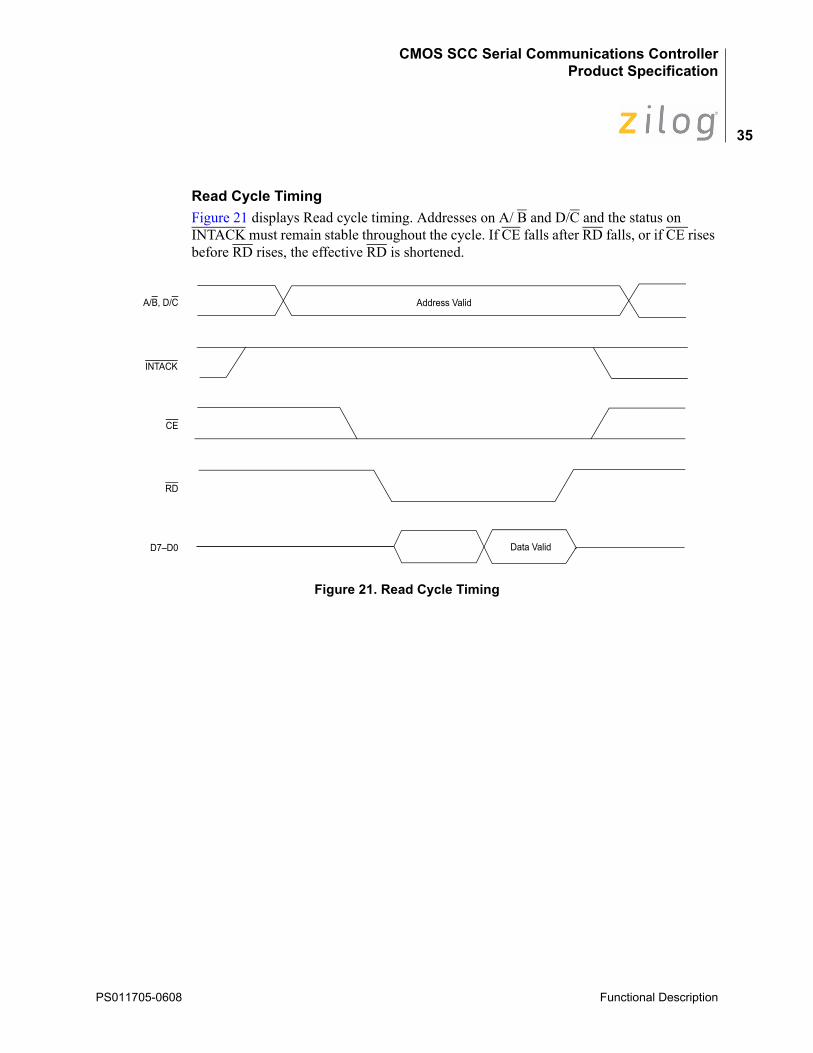
Read Cycle TimingFigure 21 displays Read cycle timing. Addresses on A/ B and D/C and the status on INTACK must remain stable throughout the cycle. If CE falls after RD falls, or if CE rises before RD rises, the effective RD is shortened.
Figure 21. Read Cycle Timing
D7–D0 Data Valid
RD
CE
INTACK
A/B, D/C Address Valid
PS011705-0608 Functional Description
CMOS SCC Serial Communications ControllerProduct Specification
36
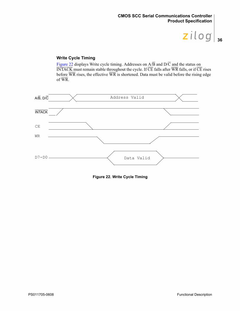
Write Cycle TimingFigure 22 displays Write cycle timing. Addresses on A/B and D/C and the status on INTACK must remain stable throughout the cycle. If CE falls after WR falls, or if CE rises before WR rises, the effective WR is shortened. Data must be valid before the rising edge of WR.
Figure 22. Write Cycle Timing
AdAddA Address Valid
Data Valid
WR
D7-D0
CE
INTACK
A/B, D/C
PS011705-0608 Functional Description
CMOS SCC Serial Communications ControllerProduct Specification
37
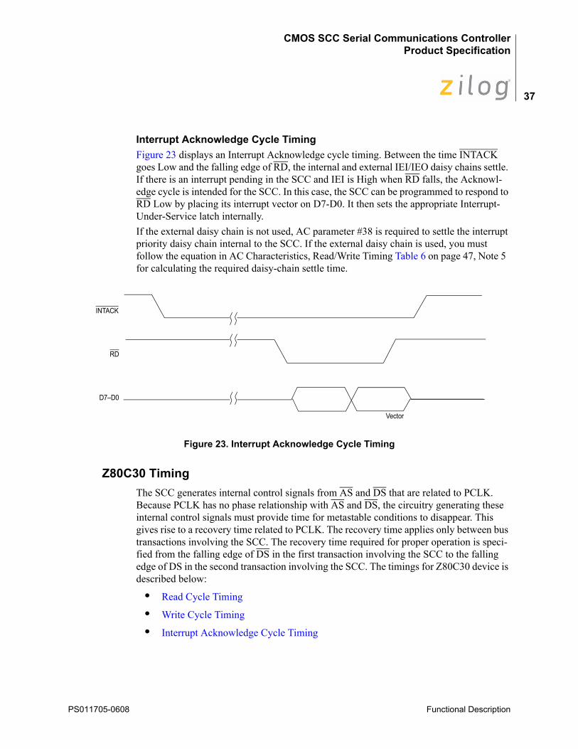
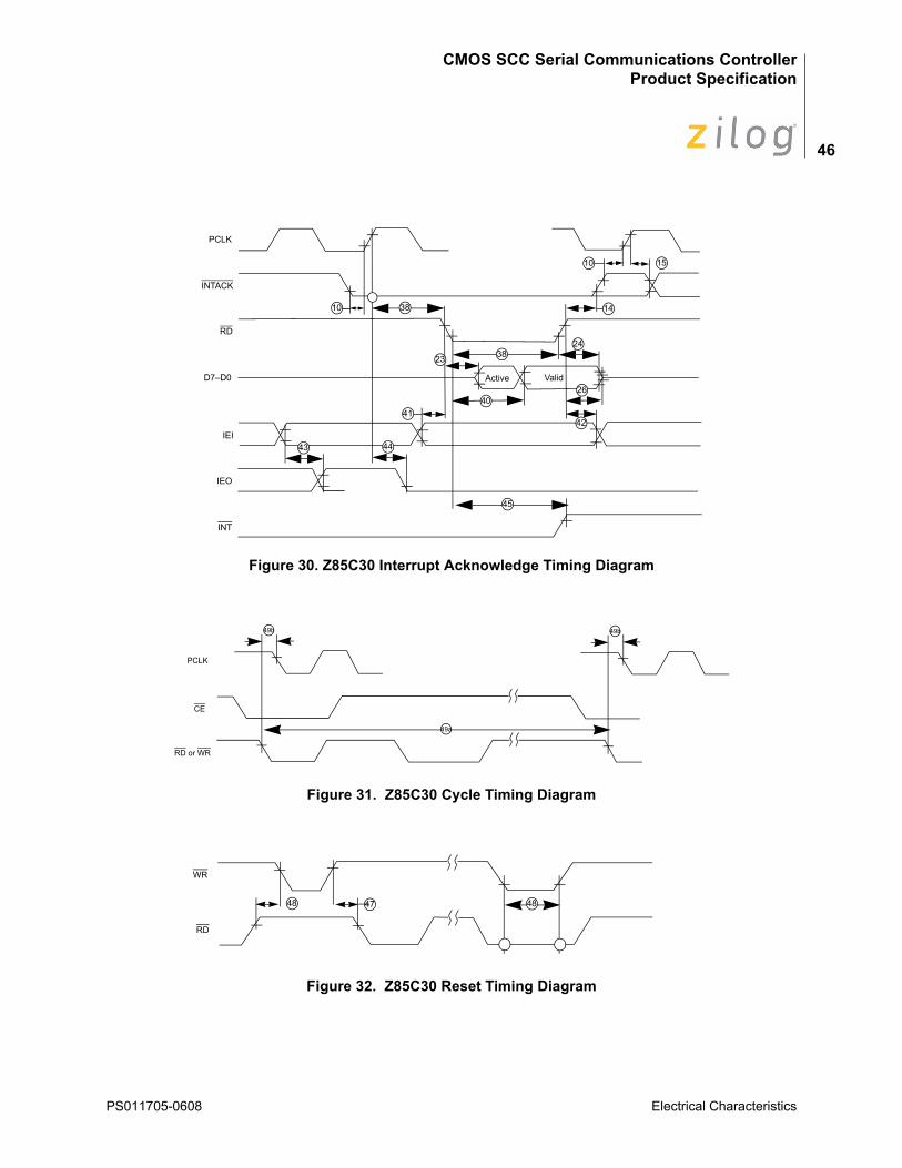
Interrupt Acknowledge Cycle TimingFigure 23 displays an Interrupt Acknowledge cycle timing. Between the time INTACK goes Low and the falling edge of RD, the internal and external IEI/IEO daisy chains settle. If there is an interrupt pending in the SCC and IEI is High when RD falls, the Acknowl-edge cycle is intended for the SCC. In this case, the SCC can be programmed to respond to RD Low by placing its interrupt vector on D7-D0. It then sets the appropriate Interrupt-Under-Service latch internally. If the external daisy chain is not used, AC parameter #38 is required to settle the interrupt priority daisy chain internal to the SCC. If the external daisy chain is used, you must follow the equation in AC Characteristics, Read/Write Timing Table 6 on page 47, Note 5 for calculating the required daisy-chain settle time.
Figure 23. Interrupt Acknowledge Cycle Timing
Z80C30 TimingThe SCC generates internal control signals from AS and DS that are related to PCLK. Because PCLK has no phase relationship with AS and DS, the circuitry generating these internal control signals must provide time for metastable conditions to disappear. This gives rise to a recovery time related to PCLK. The recovery time applies only between bus transactions involving the SCC. The recovery time required for proper operation is speci-fied from the falling edge of DS in the first transaction involving the SCC to the falling edge of DS in the second transaction involving the SCC. The timings for Z80C30 device is described below:
• Read Cycle Timing
• Write Cycle Timing
• Interrupt Acknowledge Cycle Timing
D7–D0
RD
INTACK
Vector
PS011705-0608 Functional Description

CMOS SCC Serial Communications ControllerProduct Specification
38
Read Cycle TimingFigure 24 displays the Read cycle timing. The address on AD7–AD0 and the state of CS0 and INTACK are latched by the rising edge of AS. R/W must be High to indicate a Read cycle. CS1 must also be High for the Read cycle to occur. The data bus drivers in the SCC are then enabled while DS is Low.
Figure 24. Read Cycle Timing
INTACK
DS
AS
CS0
R/W
CS1
AD7–AD0 Address Data Valid
PS011705-0608 Functional Description
CMOS SCC Serial Communications ControllerProduct Specification
39
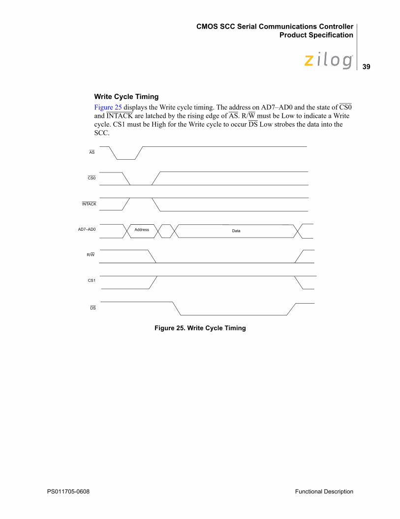
Write Cycle TimingFigure 25 displays the Write cycle timing. The address on AD7–AD0 and the state of CS0 and INTACK are latched by the rising edge of AS. R/W must be Low to indicate a Write cycle. CS1 must be High for the Write cycle to occur DS Low strobes the data into the SCC.
Figure 25. Write Cycle Timing
INTACK
DS
AS
CS0
R/W
CS1
AD7–AD0 Address Data
PS011705-0608 Functional Description
CMOS SCC Serial Communications ControllerProduct Specification
40
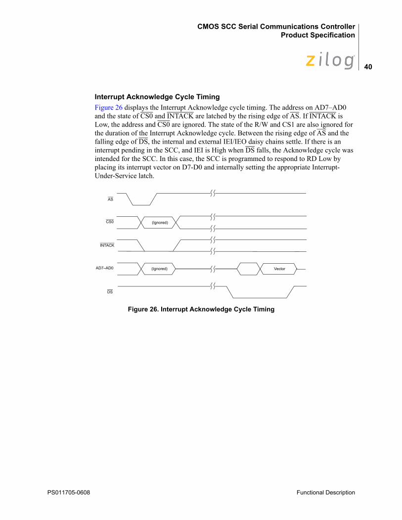
Interrupt Acknowledge Cycle TimingFigure 26 displays the Interrupt Acknowledge cycle timing. The address on AD7–AD0 and the state of CS0 and INTACK are latched by the rising edge of AS. If INTACK is Low, the address and CS0 are ignored. The state of the R/W and CS1 are also ignored for the duration of the Interrupt Acknowledge cycle. Between the rising edge of AS and the falling edge of DS, the internal and external IEI/IEO daisy chains settle. If there is an interrupt pending in the SCC, and IEI is High when DS falls, the Acknowledge cycle was intended for the SCC. In this case, the SCC is programmed to respond to RD Low by placing its interrupt vector on D7-D0 and internally setting the appropriate Interrupt-Under-Service latch.
Figure 26. Interrupt Acknowledge Cycle Timing
AD7–AD0
DS
(Ignored)
(Ignored) Vector
AS
CS0
INTACK
PS011705-0608 Functional Description
CMOS SCC Serial Communications ControllerProduct Specification
41
Electrical CharacteristicsThe electrical characteristics of the Z80C30 and the Z85C30 devices are described in the following sections.
Absolute Maximum RatingsStresses greater than those listed in Table 3 may cause permanent damage to the device This is a stress rating only. Operation of the device at any condition above those indicated in the operational sections of these specifications is not implied. Exposure to absolute maximum rating conditions for extended periods may affect device reliability.
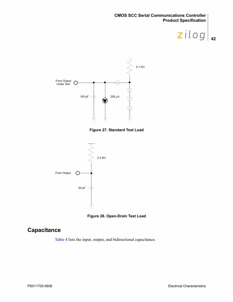
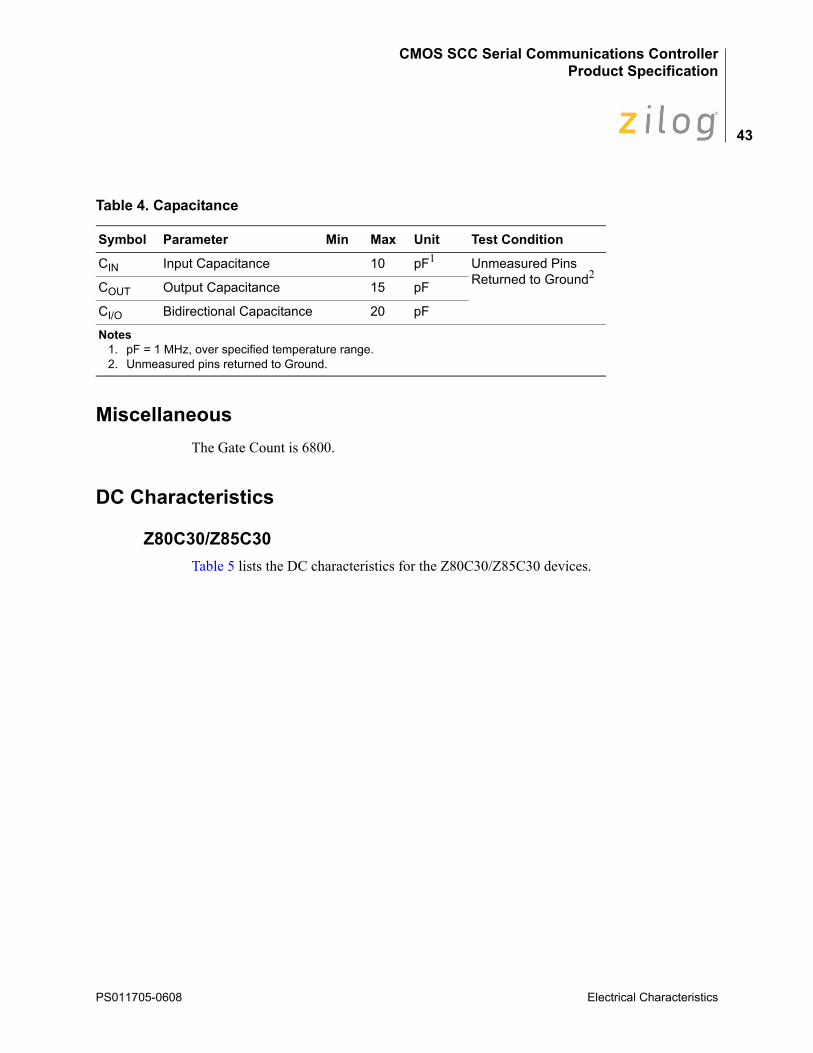
Standard Test ConditionsThe DC Characteristics and capacitance sections below apply for the following standard test conditions, unless otherwise noted. All voltages are referenced to GND. Positive current flows into the referenced pin. See Figure 27 and Figure 28.
• +4.50 V ≤ Vcc ≤ + 5.50 V
• GND = 0 V
• TA as specified in Ordering Information
Table 3. Absolute Maximum Ratings
Vcc Supply Voltage range -0.3 V to +7.0 V
Voltages on all pins with respect to GND -3 V to VCC +0.3 V
TA Operating Ambient Temperature See Ordering Information
Storage Temperature -65 °C to +150 °C
PS011705-0608 Electrical Characteristics
CMOS SCC Serial Communications ControllerProduct Specification
42
Figure 27. Standard Test Load
Figure 28. Open-Drain Test Load
CapacitanceTable 4 lists the input, output, and bidirectional capacitance.
100 pF 250 μA
2.1 KΩ
From OutputUnder Test
From Output
50 pF
2.2 KΩ
PS011705-0608 Electrical Characteristics
CMOS SCC Serial Communications ControllerProduct Specification
43
MiscellaneousThe Gate Count is 6800.
DC Characteristics
Z80C30/Z85C30Table 5 lists the DC characteristics for the Z80C30/Z85C30 devices.
Table 4. Capacitance
Symbol Parameter Min Max Unit Test Condition
CIN Input Capacitance 10 pF1 Unmeasured Pins Returned to Ground2
COUT Output Capacitance 15 pF
CI/O Bidirectional Capacitance 20 pF
Notes1. pF = 1 MHz, over specified temperature range.2. Unmeasured pins returned to Ground.
PS011705-0608 Electrical Characteristics
CMOS SCC Serial Communications ControllerProduct Specification
44
AC Characteristics
Z85C30 Read/Write Timing DiagramsFigure 29 through Figure 32 display the Z85C30 Read/Write timing diagrams. Table 6 lists the Z85C30 Read/Write timing parameters.
Table 5. Z80C30/Z85C30 DC Characteristics
Symbol Parameter Min Typ Max Unit Condition
VIH Input High Voltage 2.2 VCC +0.31 V
VIL Input Low Voltage -0.3 0.8 V
VOH1 Output High Voltage 2.4 V IOH = -1.6 mA
VOH2 Output High Voltage VCC -0.8
V IOH = -250 μA
VOL Output Low Voltage 0.4 V IOL = +2.0 mA
IIL Input Leakage ±10.0 μA 0.4 VIN + 2.4 V
IOL Output Leakage ±10.0 μA 0.4 VOUT + 2.4 V
ICC1 VCC Supply Current2 7 12 (10 MHz) mA VCC = 5 V VIH = 4.8 VIL = 0
9 15 (16.384 MHz) mA Crystal Oscillator off
ICCOSC Crystal OSC Current3 4 mA Current for each OSC in addition to ICC1
Notes1. VCC = SV t10% unless otherwise specified, over specified temperature range.2. Typical ICC was measured with oscillator off.3. No ICC (OSC) max is specified due to dependency on external circuit and frequency of oscillation.
PS011705-0608 Electrical Characteristics
CMOS SCC Serial Communications ControllerProduct Specification
45
Figure 29. Z85C30 Read/Write Timing Diagram
PCLK
A/B, D/C
INTACK
CE
RD
D7–D0Read
WR
D7–D0Write
W/REQWait
W/REQRequest
DTR/REQRequest
INT
6
1
2
5
11
13
10
16
1922
Active Valid23
2527
28
3129
32
3334
37
35
36
2426
17
20
30
3 4
7 10
15
18
12
14
9
21
PS011705-0608 Electrical Characteristics
CMOS SCC Serial Communications ControllerProduct Specification
46
Figure 30. Z85C30 Interrupt Acknowledge Timing Diagram
Figure 31. Z85C30 Cycle Timing Diagram
Figure 32. Z85C30 Reset Timing Diagram
D7–D0
INT
PCLK
INTACK
RD
IEI
IEO
41
3810
23
Active Valid
10
14
24
26
42
40
38
15
45
4443
CE
49b 49b
49a
PCLK
RD or WR
48
RD
WR
47 48
PS011705-0608 Electrical Characteristics
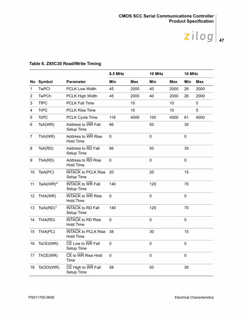
CMOS SCC Serial Communications ControllerProduct Specification
47
Table 6. Z85C30 Read/Write Timing
No Symbol Parameter
8.5 MHz 10 MHz 16 MHz
Min Max Min Max Min Max
1 TwPCI PCLK Low Width 45 2000 40 2000 26 2000
2 TwPCh PCLK High Width 45 2000 40 2000 26 2000
3 TfPC PCLK Fall Time 10 10 5
4 TrPC PCLK Rise Time 10 10 5
5 TcPC PCLK Cycle Time 118 4000 100 4000 61 4000
6 TsA(WR) Address to WR Fall Setup Time
66 50 35
7 ThA(WR) Address to WR Rise Hold Time
0 0 0
8 TsA(RD) Address to RD Fall Setup Time
66 50 35
9 ThA(RD) Address to RD Rise Hold Time
0 0 0
10 TsiA(PC) INTACK to PCLK Rise Setup Time
20 20 15
11 TsiAi(WR)a INTACK to WR Fall Setup Time
140 120 70
12 ThIA(WR) INTACK to WR Rise Hold Time
0 0 0
13 TsiAi(RD)1 INTACK to RD Fall Setup Time
140 120 70
14 ThIA(RD) INTACK to RD Rise Hold Time
0 0 0
15 ThIA(PC) INTACK to PCLK Rise Hold Time
38 30 15
16 TsCEI(WR) CE Low to WR Fall Setup Time
0 0 0
17 ThCE(WR) CE to WR Rise Hold Time
0 0 0
18 TsCEh(WR) CE High to WR Fall Setup Time
58 50 30
PS011705-0608 Electrical Characteristics
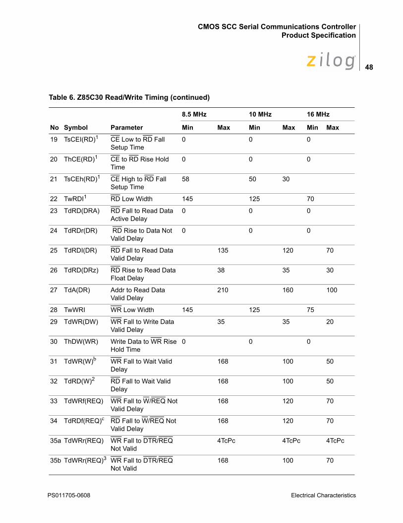
CMOS SCC Serial Communications ControllerProduct Specification
48
19 TsCEI(RD)1 CE Low to RD Fall Setup Time
0 0 0
20 ThCE(RD)1 CE to RD Rise Hold Time
0 0 0
21 TsCEh(RD)1 CE High to RD Fall Setup Time
58 50 30
22 TwRDI1 RD Low Width 145 125 70
23 TdRD(DRA) RD Fall to Read Data Active Delay
0 0 0
24 TdRDr(DR) RD Rise to Data Not Valid Delay
0 0 0
25 TdRDI(DR) RD Fall to Read Data Valid Delay
135 120 70
26 TdRD(DRz) RD Rise to Read Data Float Delay
38 35 30
27 TdA(DR) Addr to Read Data Valid Delay
210 160 100
28 TwWRI WR Low Width 145 125 75
29 TdWR(DW) WR Fall to Write Data Valid Delay
35 35 20
30 ThDW(WR) Write Data to WR Rise Hold Time
0 0 0
31 TdWR(W)b WR Fall to Wait Valid Delay
168 100 50
32 TdRD(W)2 RD Fall to Wait Valid Delay
168 100 50
33 TdWRf(REQ) WR Fall to W/REQ Not Valid Delay
168 120 70
34 TdRDf(REQ)c RD Fall to W/REQ Not Valid Delay
168 120 70
35a TdWRr(REQ) WR Fall to DTR/REQ Not Valid
4TcPc 4TcPc 4TcPc
35b TdWRr(REQ)3 WR Fall to DTR/REQ Not Valid
168 100 70
Table 6. Z85C30 Read/Write Timing (continued)
No Symbol Parameter
8.5 MHz 10 MHz 16 MHz
Min Max Min Max Min Max
PS011705-0608 Electrical Characteristics

CMOS SCC Serial Communications ControllerProduct Specification
49
36 TdRDrrREQ) RD Rise to DTR/REQ Not Valid Delay
NA NA NA
37 TdPC(INT) PCLK Fall to INT Valid Delay
500 320 175
38 TdIAi(RD)d INTACK to RD Fall (Ack) Delay
145 90 50
39 TwRDA RD (Acknowledge) Width
145 125 75
40 TdRDA(DR) RD Fall (Ack) to Read Data Valid Delay
135 120 70
41 TsiEI(RDA) IEI to RD Fall (Ack) Setup Time
95 80 50
42 ThIEI(RDA) IEI to RD Rise (Ack) Hold Time
0 0 0
43 TdIElrIEO) IEI to IEO Delay Time 95 80 45
44 TdPC(IEO) PCLK Rise to IEO Delay
195 175 80
45 TdRDA(INT)2 RD Fall to INT Inactive Delay
480 320 200
46 TdRDrWRQ) RD Rise to WR Fall Delay for No Reset
15 15 10
47 TdWRQ(RD) WR Rise to RD Fall Delay for No Reset
15 15 10
48 TwRES WR and RD Low for Reset
145 100 75
49a Trce Valid Access Recovery Time
3.5TcPc 3.5TcPc 3.5TcPc
Table 6. Z85C30 Read/Write Timing (continued)
No Symbol Parameter
8.5 MHz 10 MHz 16 MHz
Min Max Min Max Min Max
PS011705-0608 Electrical Characteristics
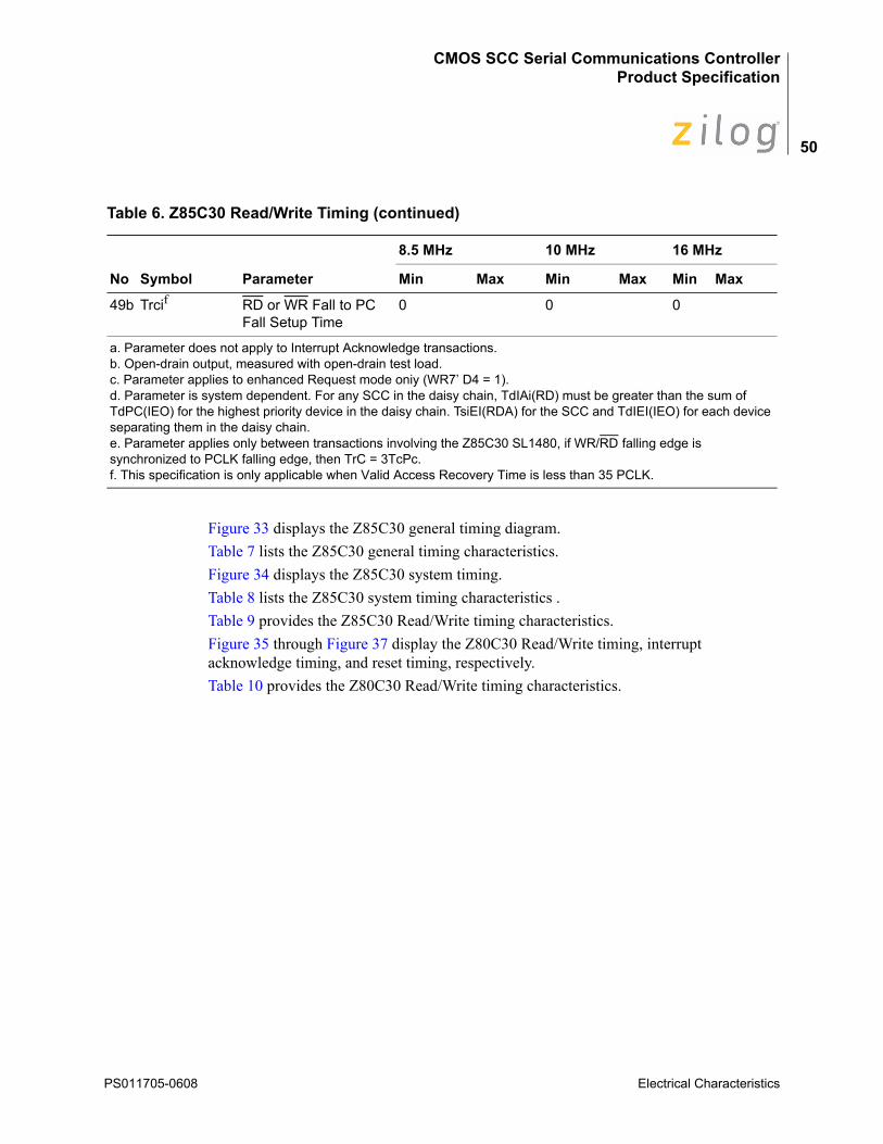
CMOS SCC Serial Communications ControllerProduct Specification
50
Figure 33 displays the Z85C30 general timing diagram. Table 7 lists the Z85C30 general timing characteristics. Figure 34 displays the Z85C30 system timing.Table 8 lists the Z85C30 system timing characteristics . Table 9 provides the Z85C30 Read/Write timing characteristics.Figure 35 through Figure 37 display the Z80C30 Read/Write timing, interrupt acknowledge timing, and reset timing, respectively.Table 10 provides the Z80C30 Read/Write timing characteristics.
49b Trcif RD or WR Fall to PC Fall Setup Time
0 0 0
a. Parameter does not apply to Interrupt Acknowledge transactions.b. Open-drain output, measured with open-drain test load.c. Parameter applies to enhanced Request mode oniy (WR7’ D4 = 1).d. Parameter is system dependent. For any SCC in the daisy chain, TdIAi(RD) must be greater than the sum of TdPC(IEO) for the highest priority device in the daisy chain. TsiEI(RDA) for the SCC and TdIEI(IEO) for each device separating them in the daisy chain.e. Parameter applies only between transactions involving the Z85C30 SL1480, if WR/RD falling edge is synchronized to PCLK falling edge, then TrC = 3TcPc.f. This specification is only applicable when Valid Access Recovery Time is less than 35 PCLK.
Table 6. Z85C30 Read/Write Timing (continued)
No Symbol Parameter
8.5 MHz 10 MHz 16 MHz
Min Max Min Max Min Max
PS011705-0608 Electrical Characteristics
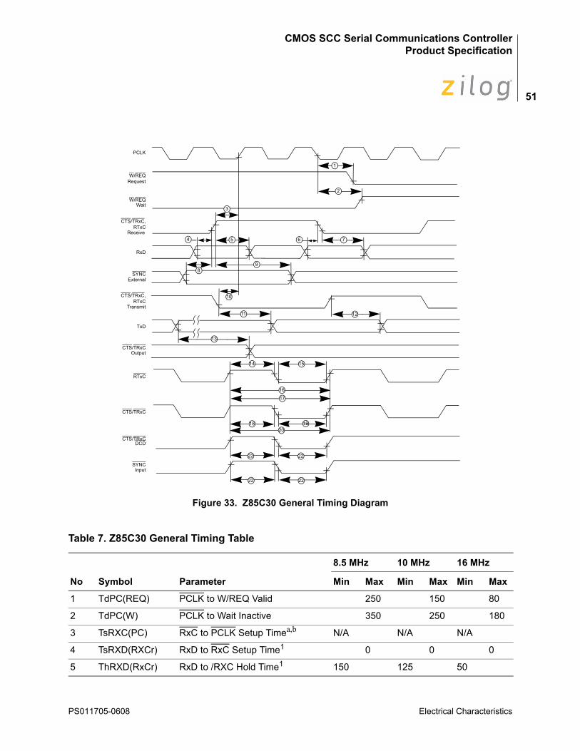
CMOS SCC Serial Communications ControllerProduct Specification
51
Figure 33. Z85C30 General Timing Diagram
Table 7. Z85C30 General Timing Table
No Symbol Parameter
8.5 MHz 10 MHz 16 MHz
Min Max Min Max Min Max
1 TdPC(REQ) PCLK to W/REQ Valid 250 150 80
2 TdPC(W) PCLK to Wait Inactive 350 250 180
3 TsRXC(PC) RxC to PCLK Setup Timea,b N/A N/A N/A
4 TsRXD(RXCr) RxD to RxC Setup Time1 0 0 0
5 ThRXD(RxCr) RxD to /RXC Hold Time1 150 125 50
SYNCInput
CTS/TRxCDCD
CTS/TRxC
RTxC
CTS/TRxCOutput
22 22
22 22
2018 19
16
17
14 15
1
2
6 74 5
89
3
1211
13
TxD
RTxCTransmit
CTS/TRxC,
SYNCExternal
10
RxD
RTxCReceive
CTS/TRxC,
W/REQWait
W/REQRequest
PCLK
PS011705-0608 Electrical Characteristics
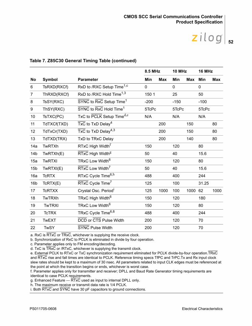
CMOS SCC Serial Communications ControllerProduct Specification
52
6 TsRXD(RXCf) RxD to /RXC Setup Time1,c 0 0 0
7 ThRXD(RXCf) RxD to /RXC Hold Time1,3 150 1 25 50
8 TsSY(RXC) SYNC to RxC Setup Time1 -200 -150 -100
9 ThSY(RXC) SYNC to RxC Hold Time1 5TcPc 5TcPc 5TcPc
10 TsTXC(PC) TxC to PCLK Setup Timed,e N/A N/A N/A
11 TdTXCf(TXD) TxC to TxD Delay4 200 150 80
12 TdTxCr(TXD) TxC to TxD Delay4,3 200 150 80
13 TdTXD(TRX) TxD to TRxC Delay 200 140 80
14a TwRTXh RTxC High Widthf 150 120 80
14b TwRTXh(E) RTxC High Widthg 50 40 15.6
15a TwRTXI TRxC Low Width6 150 120 80
15b TwRTXI(E) RTxC Low Width7 50 40 15.6
16a TcRTX RTxC Cycle Time6,h 488 400 244
16b TcRTX(E) RTxC Cycle Time7 125 100 31.25
17 TcRTXX Crystal Osc. Periodi 125 1000 100 1000 62 1000
18 TwTRXh TRxC High Width6 150 120 180
19 TwTRXI TRxC Low Width6 150 120 80
20 TcTRX TRxC Cycle Time6,8 488 400 244
21 TwEXT DCD or CTS Pulse Width 200 120 70
22 TwSY SYNC Pulse Width 200 120 70
a. RxC is RTxC or TRxC, whichever is supplying the receive clock.b. Synchronization of RxC to PCLK is eliminated in divide by four operation.c. Parameter applies only to FM encoding/decoding.d. TxC is TRxC or /RTxC, whichever is supplying the transmit clock.e. External PCLK to RTxC or TxC synchronization requirement eliminated for PCLK divide-by-four operation.TRxC and RTxC rise and fall times are identical to PCLK. Reference timing specs TfPC and TrPC.Tx and Rx input clock slew rates should be kept to a maximum of 30 nsec. All parameters related to input CLK edges must be referenced at the point at which the transition begins or ends, whichever is worst case.f. Parameter applies only for transmitter and receiver; DPLL and Baud Rate Generator timing requirements are identical to case PCLK requirements.g. Enhanced Feature — RTxC used as input to internal DPLL only.h. The maximum receive or transmit data rate is 1/4 PCLK.i. Both RTxC and SYNC have 30 pF capacitors to ground connections.
Table 7. Z85C30 General Timing Table (continued)
No Symbol Parameter
8.5 MHz 10 MHz 16 MHz
Min Max Min Max Min Max
PS011705-0608 Electrical Characteristics
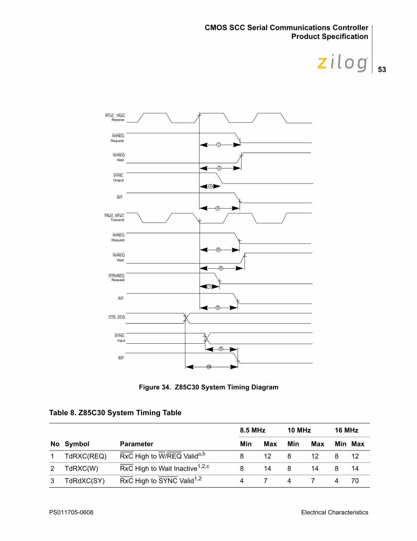
CMOS SCC Serial Communications ControllerProduct Specification
53
Figure 34. Z85C30 System Timing Diagram
Table 8. Z85C30 System Timing Table
No Symbol Parameter
8.5 MHz 10 MHz 16 MHz
Min Max Min Max Min Max
1 TdRXC(REQ) RxC High to W/REQ Valida,b 8 12 8 12 8 12
2 TdRXC(W) RxC High to Wait Inactive1,2,c 8 14 8 14 8 14
3 TdRdXC(SY) RxC High to SYNC Valid1,2 4 7 4 7 4 70
10
INT
SYNCInput
INT
CTS, DCD
DTR/REQRequest
WaitW/REQ
RequestW/REQ
TRxC, RTxCTransmit
INT
SYNCOutput
WaitW/REQ
RequestW/REQ
RTxC, TRxCReceive
9
8
7
6
6
4
3
1
2
PS011705-0608 Electrical Characteristics
CMOS SCC Serial Communications ControllerProduct Specification
54
4 TsRXC(INT) RxC High to INT Valid 1,2,3 10 16 10 16 10 16
5 TdTXC(REQ) TxC Low to W/REQ Valid2,d 5 8 5 8 5 8
6 TdTXC(W) TxC Low to Wait Inactive2,3,4 5 11 5 11 5 11
7 TdTXC(DRQ) TxC Low to DTR/REQ Valid3,4 4 7 4 7 4 7
8 TdTXC(INT) TxC Low to INT Valid2,3,4 6 10 6 10 6 10
9a TdSY(INT) SYNC to INT Valid 2,3 2 6 2 6 2 6
9b TdSY(INT) SYNC to INT Valid2,3,e 2 3 2 3 2 3
10 TdEXT(INT) DCD or CTS to INT Valid2,3 2 6 2 6 2 6
a. RxC is RTxC or TRxC, whichever is supplying the receive clock.b. Units equal to TcPc.c. Open-drain output, measured with open-drain test load.d. TxC is TRxC or RTxC whichever is supplying the transmit clock.e. Units equal to AS.
Table 9. Z85C30 Read/Write Timing
No Symbol Parameter
8.5 MHz 10 MHz 16 MHz
Min Max Min Max Min Max
1 TwPCI PCLK Low Width 45 2000 40 2000 26 2000
2 TwPCh PCLK High Width 45 2000 40 2000 26 2000
3 TfPC PCLK Fail Time 10 10 5
4 TrPC PCLK Rise Time 10 10 5
5 TcPC PCLK Cycle Time 118 4000 100 4000 61 4000
6 TsA(WR) Address to WR Fail Setup Time 66 50 35
7 ThA(WR) Address to WR Rise Hold Time 0 0 0
8 TsA(RD) Address to RD Fall Setup Time 66 50 35
9 ThA(RD) Address to RD Rise Hold Time 0 0 0
10 TsiA(PC) INTACK to PCLK Rise Setup Time 20 20 15
Table 8. Z85C30 System Timing Table (continued)
No Symbol Parameter
8.5 MHz 10 MHz 16 MHz
Min Max Min Max Min Max
PS011705-0608 Electrical Characteristics
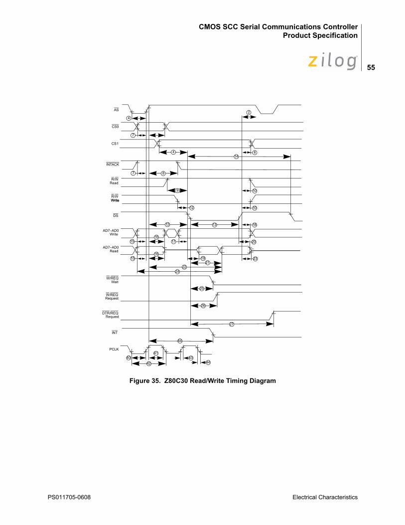
CMOS SCC Serial Communications ControllerProduct Specification
55
Figure 35. Z80C30 Read/Write Timing Diagram
Wait
W/REQ
Request
PCLK
4240
4143
44
44
27
INT
DTR/REQ
Request
W/REQ
25
26
2422
15
1516
17
16
12 13
1921
AD7–AD0Read
AD7–AD0Write
DS
12
WriteR/WWrite
R/WRead
INTACK
7 8
9
CS1
CS0
7
4
414
6
10
10
18
20
23
2AS
PS011705-0608 Electrical Characteristics

CMOS SCC Serial Communications ControllerProduct Specification
56
Figure 36. Z80C30 Interrupt Acknowledge Timing Diagram
Figure 37. Z80C30 Reset Timing Diagram
Table 10. Z80C30 Read/Write Timinga
No Symbol Parameter
8 MHz 10 MHz
Min Max Min Max
1 TwAS AS Low Width 35 30
2 TdDS(AS) DS Rise to AS Fall Delayb 15 10
3 TsCSO(AS) CS0 to AS Rise Setup Time2 0 0
4 ThCSO(AS) CS0 to AS Rise Hold Time2 30 20
INT
IEO
IEI
36
3534
3231 22
33
2030
19
29
8
7
AD7–AD0
DS
INTACK
AS
DS
AS
37 3835
PS011705-0608 Electrical Characteristics
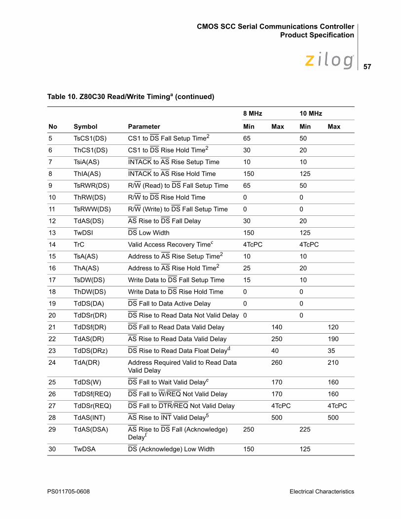
CMOS SCC Serial Communications ControllerProduct Specification
57
5 TsCS1(DS) CS1 to DS Fall Setup Time2 65 50
6 ThCS1(DS) CS1 to DS Rise Hold Time2 30 20
7 TsiA(AS) INTACK to AS Rise Setup Time 10 10
8 ThIA(AS) INTACK to AS Rise Hold Time 150 125
9 TsRWR(DS) R/W (Read) to DS Fall Setup Time 65 50
10 ThRW(DS) R/W to DS Rise Hold Time 0 0
11 TsRWW(DS) R/W (Write) to DS Fall Setup Time 0 0
12 TdAS(DS) AS Rise to DS Fall Delay 30 20
13 TwDSI DS Low Width 150 125
14 TrC Valid Access Recovery Timec 4TcPC 4TcPC
15 TsA(AS) Address to AS Rise Setup Time2 10 10
16 ThA(AS) Address to AS Rise Hold Time2 25 20
17 TsDW(DS) Write Data to DS Fall Setup Time 15 10
18 ThDW(DS) Write Data to DS Rise Hold Time 0 0
19 TdDS(DA) DS Fall to Data Active Delay 0 0
20 TdDSr(DR) DS Rise to Read Data Not Valid Delay 0 0
21 TdDSf(DR) DS Fall to Read Data Valid Delay 140 120
22 TdAS(DR) AS Rise to Read Data Valid Delay 250 190
23 TdDS(DRz) DS Rise to Read Data Float Delayd 40 35
24 TdA(DR) Address Required Valid to Read Data Valid Delay
260 210
25 TdDS(W) DS Fall to Wait Valid Delaye 170 160
26 TdDSf(REQ) DS Fall to W/REQ Not Valid Delay 170 160
27 TdDSr(REQ) DS Fall to DTR/REQ Not Valid Delay 4TcPC 4TcPC
28 TdAS(INT) AS Rise to INT Valid Delay5 500 500
29 TdAS(DSA) AS Rise to DS Fall (Acknowledge) Delayf
250 225
30 TwDSA DS (Acknowledge) Low Width 150 125
Table 10. Z80C30 Read/Write Timinga (continued)
No Symbol Parameter
8 MHz 10 MHz
Min Max Min Max
PS011705-0608 Electrical Characteristics
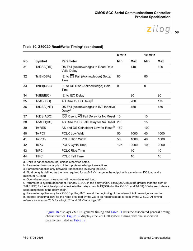
CMOS SCC Serial Communications ControllerProduct Specification
58
Figure 38 displays Z80C30 general timing and Table 11 lists the associated general timing characteristics. Figure 39 displays the Z80C30 system timing with the associated parameters listed in Table 12.
31 TdDSA(DR) DS Fall (Acknowledge) to Read Data Valid Delay
140 120
32 TsiEI(DSA) IEI to DS Fall (Acknowledge) Setup Time
80 80
33 ThIEI(DSA) IEI to DS Rise (Acknowledge) Hold Time
0 0
34 TdIEI(IEO) IEI to IEO Delay 90 90
35 TdAS(IEO) AS Rise to IEO Delayg 200 175
36 TdDSA(INT) DS Fall (Acknowledge) to INT Inactive Delay5
450 450
37 TdDS(ASQ) DS Rise to AS Fall Delay for No Reset 15 15
38 TdASQ(DS) AS Rise to DS Fall Delay for No Reset 20 15
39 TwRES AS and DS Coincident Low for Reseth 150 100
40 TwPCI PCLK Low Width 50 1000 40 1000
41 TwPCh PCLK High Width 50 1000 40 1000
42 TcPC PCLK Cycle Time 125 2000 100 2000
43 TrPC PCLK Rise Time 10 10
44 TfPC PCLK Fall Time 10 10
a. Units in nanoseconds (ns) unless otherwise noted.b. Parameter does not apply to Interrupt Acknowledge transactions.c. Parameter applies only between transactions involving the SCC.d. Float delay is defined as the time required for a ±0.5 V change in the output with a maximum DC load and a minimum AC load.e. Open-drain output, measured with open-drain test load.f. Parameter is system dependent. For any Z-SCC in the daisy chain. TdAS(DSA) must be greater than the sum of TdAS(IEO) for the highest priority device in the daisy chain TsiEI(DSA) for the Z-SCC, and TdIElf(IEO) for each device separating them in the daisy chain.g. Parameter applies only to a Z-SCC pulling INT Low at the beginning of the Interrupt Acknowledge transaction.h. Internal circuitry allows for the reset provided by the ZB to be recognized as a reset by the Z-SCC. All timing references assume 20 V for a logic “1” and 08 V for a logic “0”.
Table 10. Z80C30 Read/Write Timinga (continued)
No Symbol Parameter
8 MHz 10 MHz
Min Max Min Max
PS011705-0608 Electrical Characteristics
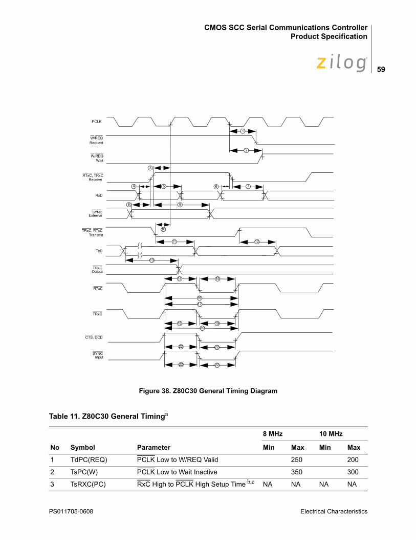
CMOS SCC Serial Communications ControllerProduct Specification
59
Figure 38. Z80C30 General Timing Diagram
Table 11. Z80C30 General Timinga
No Symbol Parameter
8 MHz 10 MHz
Min Max Min Max
1 TdPC(REQ) PCLK Low to W/REQ Valid 250 200
2 TsPC(W) PCLK Low to Wait Inactive 350 300
3 TsRXC(PC) RxC High to PCLK High Setup Time b,c NA NA NA NA
SYNCInput
22 22
22 22
CTS, DCD
TRxC
RTxC
TRxCOutput
TRxC, RTxCTransmit
SYNCExternal
RxD
RTxC, TRxCReceive
W/REQWait
W/REQRequest
PCLK
201918
16
17
14 15
13
8
11
10
9
4 5 6
3
7
1
2
12
TxD
PS011705-0608 Electrical Characteristics
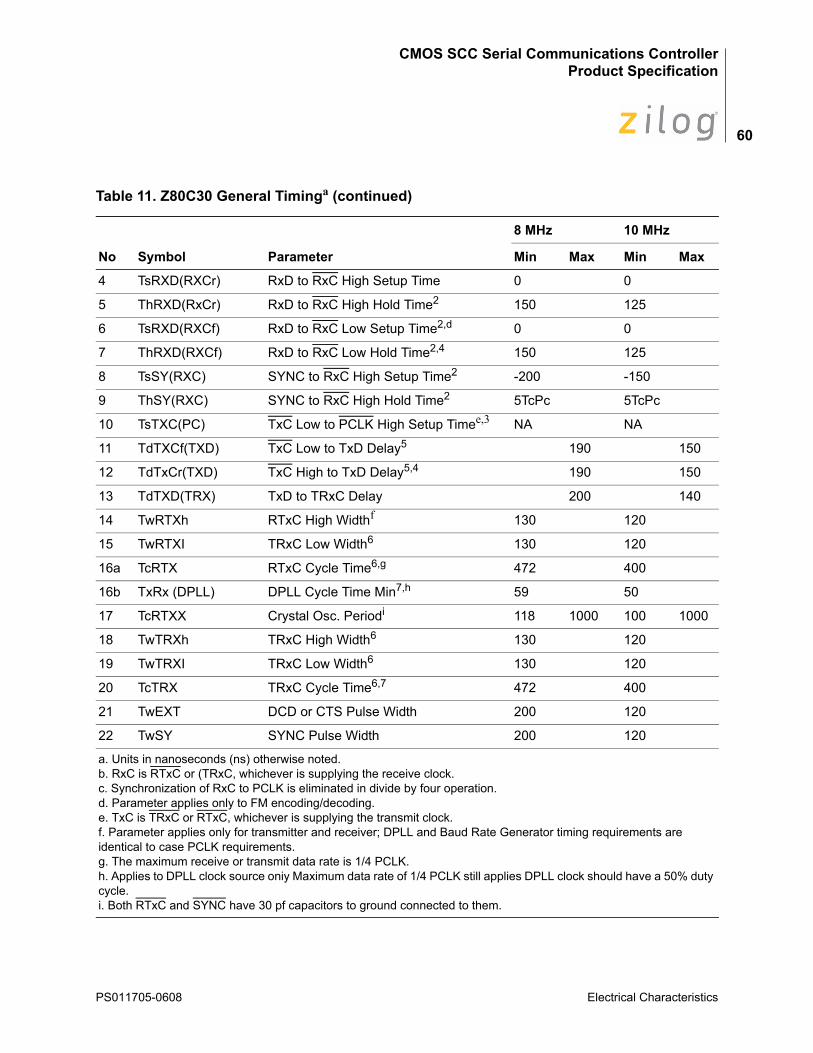
CMOS SCC Serial Communications ControllerProduct Specification
60
4 TsRXD(RXCr) RxD to RxC High Setup Time 0 0
5 ThRXD(RxCr) RxD to RxC High Hold Time2 150 125
6 TsRXD(RXCf) RxD to RxC Low Setup Time2,d 0 0
7 ThRXD(RXCf) RxD to RxC Low Hold Time2,4 150 125
8 TsSY(RXC) SYNC to RxC High Setup Time2 -200 -150
9 ThSY(RXC) SYNC to RxC High Hold Time2 5TcPc 5TcPc
10 TsTXC(PC) TxC Low to PCLK High Setup Timee,3 NA NA
11 TdTXCf(TXD) TxC Low to TxD Delay5 190 150
12 TdTxCr(TXD) TxC High to TxD Delay5,4 190 150
13 TdTXD(TRX) TxD to TRxC Delay 200 140
14 TwRTXh RTxC High Widthf 130 120
15 TwRTXI TRxC Low Width6 130 120
16a TcRTX RTxC Cycle Time6,g 472 400
16b TxRx (DPLL) DPLL Cycle Time Min7,h 59 50
17 TcRTXX Crystal Osc. Periodi 118 1000 100 1000
18 TwTRXh TRxC High Width6 130 120
19 TwTRXI TRxC Low Width6 130 120
20 TcTRX TRxC Cycle Time6,7 472 400
21 TwEXT DCD or CTS Pulse Width 200 120
22 TwSY SYNC Pulse Width 200 120
a. Units in nanoseconds (ns) otherwise noted.b. RxC is RTxC or (TRxC, whichever is supplying the receive clock.c. Synchronization of RxC to PCLK is eliminated in divide by four operation.d. Parameter applies only to FM encoding/decoding.e. TxC is TRxC or RTxC, whichever is supplying the transmit clock.f. Parameter applies only for transmitter and receiver; DPLL and Baud Rate Generator timing requirements are identical to case PCLK requirements.g. The maximum receive or transmit data rate is 1/4 PCLK.h. Applies to DPLL clock source oniy Maximum data rate of 1/4 PCLK still applies DPLL clock should have a 50% duty cycle.i. Both RTxC and SYNC have 30 pf capacitors to ground connected to them.
Table 11. Z80C30 General Timinga (continued)
No Symbol Parameter
8 MHz 10 MHz
Min Max Min Max
PS011705-0608 Electrical Characteristics
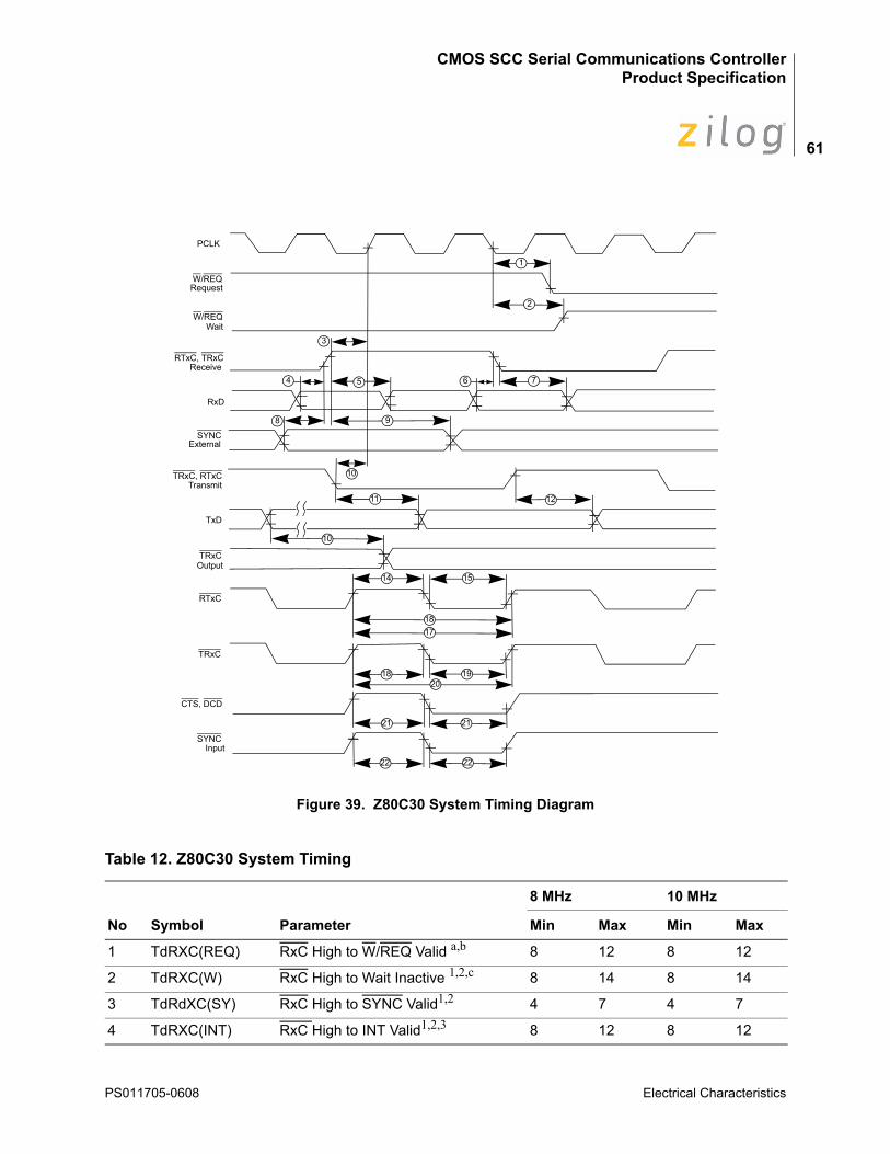
CMOS SCC Serial Communications ControllerProduct Specification
61
Figure 39. Z80C30 System Timing Diagram
Table 12. Z80C30 System Timing
No Symbol Parameter
8 MHz 10 MHz
Min Max Min Max
1 TdRXC(REQ) RxC High to W/REQ Valid a,b 8 12 8 12
2 TdRXC(W) RxC High to Wait Inactive 1,2,c 8 14 8 14
3 TdRdXC(SY) RxC High to SYNC Valid1,2 4 7 4 7
4 TdRXC(INT) RxC High to INT Valid1,2,3 8 12 8 12
SYNCInput
CTS, DCD
TRxC
RTxC
TRxCOutput
TxD
TRxC, RTxC Transmit
SYNCExternal
22 22
21 21
2018 19
1718
14 15
11
10
12
RxD
10
RTxC, TRxC Receive
W/REQWait
98
4 5
3
W/REQRequest
PCLK
6 7
2
1
PS011705-0608 Electrical Characteristics
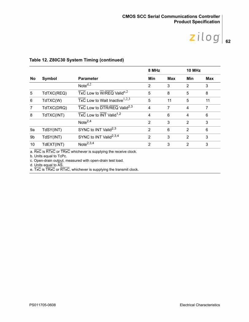
CMOS SCC Serial Communications ControllerProduct Specification
62
Noted,2 2 3 2 3
5 TdTXC(REQ) TxC Low to W/REQ Valide,2 5 8 5 8
6 TdTXC(W) TxC Low to Wait Inactive1,2,3 5 11 5 11
7 TdTXC(DRQ) TxC Low to DTR/REQ Valid2,3 4 7 4 7
8 TdTXC(INT) TxC Low to INT Valid1,2 4 6 4 6
Note2,4 2 3 2 3
9a TdSY(INT) SYNC to INT Valid2,3 2 6 2 6
9b TdSY(INT) SYNC to INT Valid2,3,4 2 3 2 3
10 TdEXT(INT) Note2,3,4 2 3 2 3
a. RxC is RTxC or TRxC whichever is supplying the receive clock.b. Units equal to TcPc.c. Open-drain output, measured with open-drain test load.d. Units equal to AS.e. TxC is TRxC or RTxC, whichever is supplying the transmit clock.
Table 12. Z80C30 System Timing (continued)
No Symbol Parameter
8 MHz 10 MHz
Min Max Min Max
PS011705-0608 Electrical Characteristics
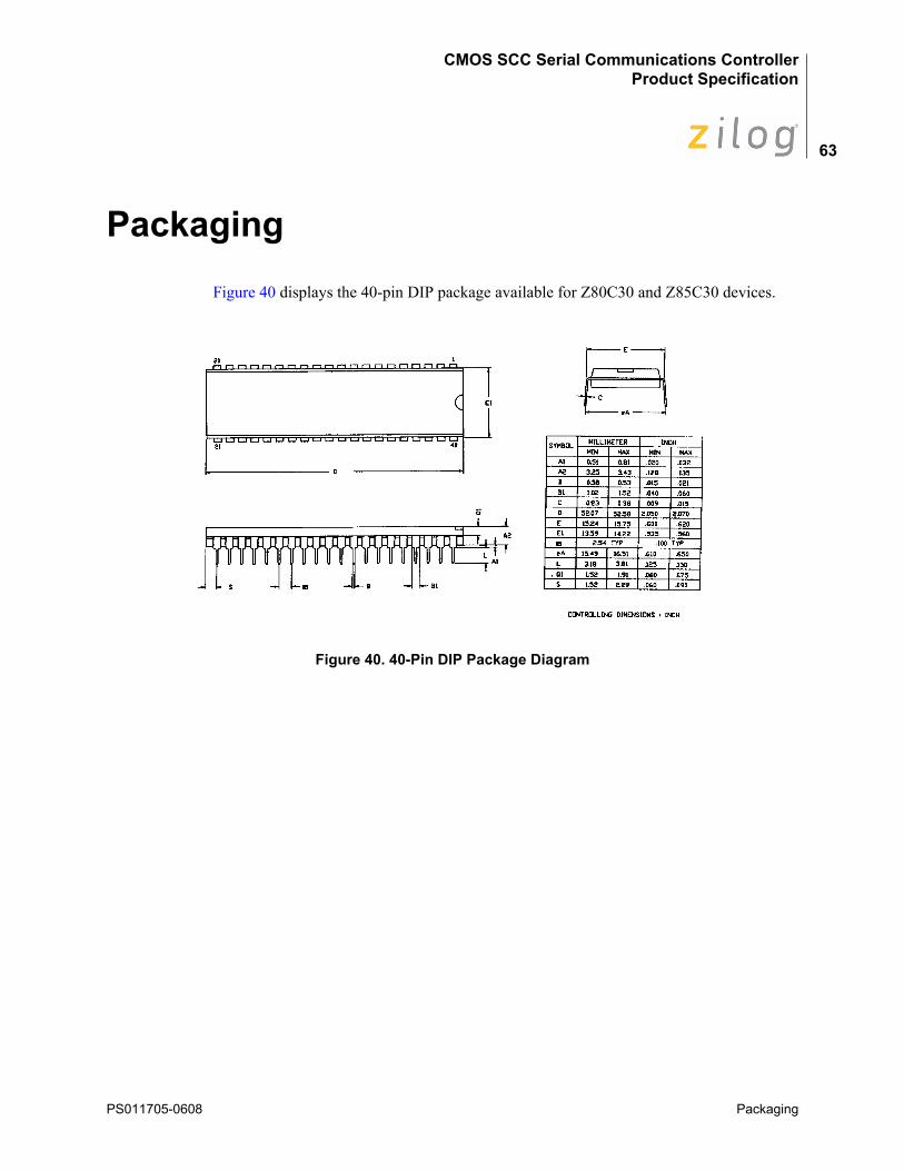
CMOS SCC Serial Communications ControllerProduct Specification
63
PackagingFigure 40 displays the 40-pin DIP package available for Z80C30 and Z85C30 devices.
Figure 40. 40-Pin DIP Package Diagram
PS011705-0608 Packaging
CMOS SCC Serial Communications ControllerProduct Specification
64
Figure 41 displays the 44-pin Plastic Leaded Chip Carriers (PLCC) package diagram available for Z80C30 and Z85C30 devices.
Figure 41. 44-Pin PLCC Package Diagram
PS011705-0608 Packaging
CMOS SCC Serial Communications ControllerProduct Specification
65
Ordering InformationTable 13 provides ordering information for the Z80C30 and the Z85C30 devices.
For complete details on Z80C30 and Z85C30 devices, development tools and downloadable software, visit www.zilog.com.
Table 13. Z80C30/Z85C30 Ordering Information
8 MHz 10 MHz 16 MHz
Z80C3008PSC Z80C3010PSC Z85C3016PSC
Z80C3008VSC Z80C3010VSC Z85C3016VSC
Z85C3008PSC/PEC Z85C3010PSC/PEC
Z85C3008VSCNEC Z85C3010VSCNEC
PS011705-0608 Packaging
CMOS SCC Serial Communications ControllerProduct Specification
66
Part Number Suffix Designations
Zilog® part numbers consist of a number of components, as indicated in the following example:
ExamplePart number Z80C3016PSG is a Z80C30, 16 MHz, PLCC, 0 ºC to +70 ºC, Lead Free
Z 80C30 16 P S GEnvironmental FlowG = Lead Free
Temperature RangeS = 0 ºC to +70 ºC E = Extended, –40 °C to +100 °C
PackageP = Plastic DIPV = Plastic Leaded Chip CarrierD = Ceramic DIP
Speed8 = 8 MHz10 = 10 MHz16 = 16 MHz
Product Number
Zilog® Prefix
PS011705-0608 Packaging
PS011705-0608 Customer Support
CMOS SCC Serial Communications ControllerProduct Specification
67
Customer SupportFor answers to technical questions about the product, documentation, or any other issues with Zilog’s offerings, please visit Zilog’s Knowledge Base at http://www.zilog.com/kb.
For any comments, detail technical questions, or reporting problems, please visit Zilog’s Technical Support at http://support.zilog.com.