tusb3410 usb to serial port controller datasheet (rev. j)
TRANSCRIPT
Product
Folder
Order
Now
Technical
Documents
Tools &
Software
Support &Community
ReferenceDesign
An IMPORTANT NOTICE at the end of this data sheet addresses availability, warranty, changes, use in safety-critical applications,intellectual property matters and other important disclaimers. PRODUCTION DATA.
TUSB3410, TUSB3410ISLLS519J –MARCH 2002–REVISED JULY 2017
TUSB3410 USB to Serial Port Controller
1 Device Overview
1
1.1 Features1• Fully Compliant With USB 2.0 Full-Speed
Specifications: TID#40340262• Supports 12-Mbps USB Data Rate (Full Speed)• Supports USB Suspend, Resume, and Remote
Wake-Up Operations• Configurable to Bus-Powered and Self-Powered
Operation• Supports a Total of Three Input and Three Output
(Interrupt, Bulk) Endpoints• Integrated 8052 Microcontroller With:
– 256 × 8 RAM for Internal Data– 10K × 8 ROM (With USB and I2C Bootloader)– 16K × 8 RAM for Code Space Loadable From
Host or I2C Port– 2K × 8 Shared RAM Used for Data Buffers and
Endpoint Descriptor Blocks (EDBs)– Master I2C Controller for EEPROM Device
Access– MCU Operates at 24 MHz, Providing 2-MIPS
Operation– 128-ms Watchdog Timer
• Enhanced UART Features:– Software and Hardware Flow Control– Automatic RS-485 Bus Transceiver Control,
With and Without Echo– Selectable IrDA Mode for Up to 115.2-kbps
Transfer– Software-Selectable Baud Rate From 50 BPS to
921.6 kbps– Programmable Serial-Interface Characteristics
– 5-, 6-, 7-, or 8-Bit Characters– Even, Odd, or No Parity-bit Generation and
Detection– 1-, 1.5-, or 2-Stop Bit Generation
– Line Break Generation and Detection– Internal Test and Loopback Capabilities– Modem Control Functions (CTS, RTS, DSR, RI
and DCD)– Internal Diagnostic Capability
– Loopback Control for CommunicationsLink-Fault Isolation
– Break, Parity, Overrun, Framing-ErrorSimulation
1.2 Applications• Modems• Peripherals:
Printers, Handheld Devices, and so on
• Medical Meters• DSP and µC Interface
1.3 DescriptionThe TUSB3410 device provides bridging between a USB port and an enhanced UART serial port. Thedevice contains an 8052 microcontroller unit (MCU) with 16KB of RAM that can be loaded from the host orfrom the external onboard memory through an I2C. The device also contains 10KB of ROM that allows theMCU to configure the USB port at boot time. The ROM code also contains an I2C bootloader. All devicefunctions (such as the USB command decoding, UART setup, and error reporting) are managed by theinternal MCU firmware in unison with the PC host.
Device InformationPART NUMBER PACKAGE BODY SIZE
TUSB3410VQFN (32) 5.00 mm × 5.00 mmLQFP (32) 7.00 mm × 7.00 mm
1. For all available packages, see the orderable addendum at the end of the data sheet.

12 MHz
Clock
Oscillator
DP, DM
PLL and
Dividers
USB
TxR
24 MHz
10K 8×
ROM
8052
Core
8 8
8
16-Bit
Timers
16K 8×
RAM
82K × 8
SRAM
8 4
Port 3
8
P3.4
P3.3
P3.1
P3.0
USB
Serial
Interface
Engine
CPU-I/F8
Suspend/
Resume
8UBM
8
USB Buffer
Manager
8
8
SIN
I C2
Controller
DMA-1
DMA-3
UART−1
SOUT
I2C Bus
RTSCTSDTRDSR
TDM
Control
Logic IR
Encoder MUX
SOUT/IR_SOUT
IRM Decoder
SIN/IR_SIN
UX
2 ×
Copyright © 2017, Texas Instruments Incorporated
2
TUSB3410, TUSB3410ISLLS519J –MARCH 2002–REVISED JULY 2017 www.ti.com
Submit Documentation FeedbackProduct Folder Links: TUSB3410
Device Overview Copyright © 2002–2017, Texas Instruments Incorporated
1.4 Functional Block Diagram
3
TUSB3410, TUSB3410Iwww.ti.com SLLS519J –MARCH 2002–REVISED JULY 2017
Submit Documentation FeedbackProduct Folder Links: TUSB3410
Revision HistoryCopyright © 2002–2017, Texas Instruments Incorporated
Table of Contents1 Device Overview ......................................... 1
1.1 Features .............................................. 11.2 Applications........................................... 11.3 Description............................................ 11.4 Functional Block Diagram ............................ 2
2 Revision History ......................................... 33 Pin Configuration and Functions..................... 4
3.1 Pin Diagrams ......................................... 44 Specifications ............................................ 6
4.1 Absolute Maximum Ratings .......................... 64.2 ESD Ratings.......................................... 64.3 Recommended Operating Conditions ................ 64.4 Thermal Information .................................. 64.5 Electrical Characteristics ............................. 74.6 Timing and Switching Characteristics Information.... 84.7 Typical Characteristics ............................... 9
5 Detailed Description .................................. 105.1 Overview ............................................ 105.2 Functional Block Diagram........................... 115.3 Device Functional Modes ........................... 115.4 Processor Subsystems.............................. 16
5.5 Memory.............................................. 245.6 Boot Modes.......................................... 67
6 Application, Implementation, and Layout ......... 846.1 Application Information.............................. 846.2 Typical Application .................................. 846.3 Layout ............................................... 886.4 Power Supply Recommendations .................. 906.5 Crystal Selection .................................... 906.6 External Circuit Required for Reliable Bus Powered
Suspend Operation ................................. 917 Device and Documentation Support ............... 92
7.1 Documentation Support ............................. 927.2 Related Links........................................ 927.3 Receiving Notification of Documentation Updates .. 927.4 Community Resources .............................. 927.5 Trademarks.......................................... 927.6 Electrostatic Discharge Caution..................... 927.7 Glossary ............................................. 92
8 Mechanical Packaging and OrderableInformation .............................................. 938.1 Packaging Information .............................. 93
2 Revision HistoryNOTE: Page numbers for previous revisions may differ from page numbers in the current version.
Changes from Revision I (November 2015) to Revision J Page
• Changed pin 21 From: DTR To: active low DTR in the Pin Functions table.................................................. 5• Changed the description of bit 7 CONT in USBCTL: USB Control Register (Addr:FFFCh), CONT= 0 From:
enabled To: disables, CONT= 1 From: disbaled To: enabled ................................................................. 40
Changes from Revision H (April 2013) to Revision I Page
• Added Pin Configuration and Functions section, ESD Ratings table, Thermal Information table, TypicalCharacteristics section, Feature Description section, Device Functional Modes, Application and Implementationsection, Power Supply Recommendations section, Layout section, Device and Documentation Support section,and Mechanical, Packaging, and Orderable Information section .............................................................. 1
• Deleted Ordering Information table. ................................................................................................ 1
4
TUSB3410, TUSB3410ISLLS519J –MARCH 2002–REVISED JULY 2017 www.ti.com
Submit Documentation FeedbackProduct Folder Links: TUSB3410
Pin Configuration and Functions Copyright © 2002–2017, Texas Instruments Incorporated
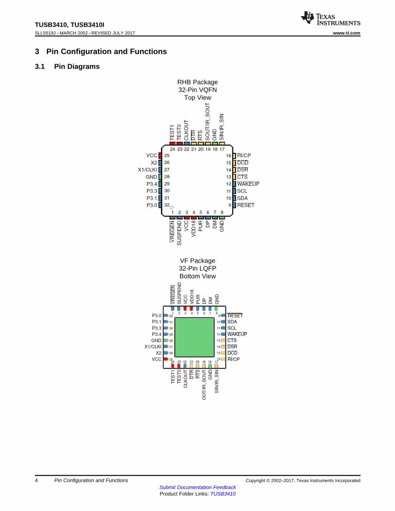
3 Pin Configuration and Functions
3.1 Pin Diagrams
RHB Package32-Pin VQFN
Top View
VF Package32-Pin LQFPBottom View
5
TUSB3410, TUSB3410Iwww.ti.com SLLS519J –MARCH 2002–REVISED JULY 2017
Submit Documentation FeedbackProduct Folder Links: TUSB3410
Pin Configuration and FunctionsCopyright © 2002–2017, Texas Instruments Incorporated
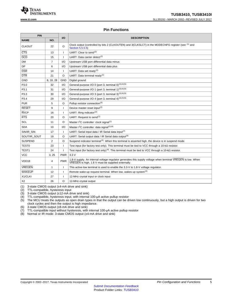
(1) 3-state CMOS output (±4-mA drive and sink)(2) TTL-compatible, hysteresis input(3) 3-state CMOS output (±12-mA drive and sink)(4) TTL-compatible, hysteresis input, with internal 100-µA active pullup resistor(5) The MCU treats the outputs as open drain types in that the output can be driven low continuously, but a high output is driven for two
clock cycles and then the output is high impedance.(6) 3-state CMOS output (±8-mA drive and sink)(7) TTL-compatible input without hysteresis, with internal 100-µA active pullup resistor(8) Normal or IR mode: 3-state CMOS output (±4-mA drive and sink)
Pin FunctionsPIN
I/O DESCRIPTIONNAME NO.
CLKOUT 22 O Clock output (controlled by bits 2 (CLKOUTEN) and 3(CLKSLCT) in the MODECNFG register (see (1) andSection 5.5.5.5)
CTS 13 I UART: Clear to send (2)
DCD 15 I UART: Data carrier detect (2)
DM 7 I/O Upstream USB port differential data minus
DP 6 I/O Upstream USB port differential data plus
DSR 14 I UART: Data set ready (2)
DTR 21 O UART: Data terminal ready (1)
GND 8, 18, 28 GND Digital ground
P3.0 32 I/O General-purpose I/O 0 (port 3, terminal 0) (3) (4) (5)
P3.1 31 I/O General-purpose I/O 1 (port 3, terminal 1) (3) (4) (5)
P3.3 30 I/O General-purpose I/O 3 (port 3, terminal 3) (3) (4) (5)
P3.4 29 I/O General-purpose I/O 4 (port 3, terminal 4) (3) (4) (5)
PUR 5 O Pullup resistor connection (6)
RESET 9 I Device master reset input (2)
RI/CP 16 I UART: Ring indicator (2)
RTS 20 O UART: Request to send (1)
SCL 11 O Master I2C controller: clock signal (1)
SDA 10 I/O Master I2C controller: data signal(1) (4)
SIN/IR_SIN 17 I UART: Serial input data / IR Serial data input (7)
SOUT/IR_SOUT 19 O UART: Serial output data / IR Serial data output (8)
SUSPEND 2 O Suspend indicator terminal (3). When this terminal is asserted high, the device is in suspend mode.
TEST0 23 I Test input (for factory test only). This terminal must be tied to VCC through a 10-kΩ resistor.
TEST1 24 I Test input (for factory test only) (4). This terminal must be tied to VCC through a 10-kΩ resistor.
VCC 3, 25 PWR 3.3 V
VDD18 4 PWR 1.8-V supply. An internal voltage regulator generates this supply voltage when terminal VREGEN is low. WhenVREGEN is high, 1.8 V must be supplied externally.
VREGEN 1 I This active-low terminal is used to enable the 3.3-V to 1.8-V voltage regulator.
WAKEUP 12 I Remote wake-up request terminal. When low, wakes up system (4)
X1/CLKI 27 I 12-MHz crystal input or clock input
X2 26 O 12-MHz crystal output
6
TUSB3410, TUSB3410ISLLS519J –MARCH 2002–REVISED JULY 2017 www.ti.com
Submit Documentation FeedbackProduct Folder Links: TUSB3410
Specifications Copyright © 2002–2017, Texas Instruments Incorporated
(1) Stresses beyond those listed under Absolute Maximum Ratings may cause permanent damage to the device. These are stress ratingsonly, and functional operation of the device at these or any other conditions beyond those indicated under Recommended OperatingConditions is not implied. Exposure to absolute-maximum-rated conditions for extended periods may affect device reliability.
4 Specifications
4.1 Absolute Maximum Ratingsover operating free-air temperature range (unless otherwise noted) (1)
MIN MAX UNITVCC Supply voltage −0.5 3.6 VVI Input voltage −0.5 VCC + 0.5 VVO Output voltage −0.5 VCC + 0.5 VIIK Input clamp current ±20 mAIOK Output clamp current ±20 mA
Tstg Storage temperatureIndustrial –65 150
°CStandard –55 150
(1) JEDEC document JEP155 states that 500-V HBM allows safe manufacturing with a standard ESD control process.(2) JEDEC document JEP157 states that 250-V CDM allows safe manufacturing with a standard ESD control process.
4.2 ESD RatingsVALUE UNIT
VESDElectrostatic discharge (ESD)performance
Human Body Model (HBM), per ANSI/ESDA/JEDEC JS001 (1) ±2000 VCharged Device Model (CDM),per JESD22-C101 (2) All pins ±500 V
4.3 Recommended Operating ConditionsMIN TYP MAX UNIT
VCC Supply voltage 3 3.3 3.6 VVI Input voltage 0 VCC V
VIH High-level input voltageTTL 2 VCC VCMOS 0.7 × VCC VCC
VIL Low-level input voltageTTL 0 0.8
VCMOS 0 0.2 × VCC
TA Operating temperatureCommercial range 0 70 °CIndustrial range –40 85 °C
(1) For more information about traditional and new thermal metrics, see the Semiconductor and C Package Thermal Metrics applicationreport.
4.4 Thermal Information
THERMAL METRIC (1)TUSB3410
UNITRHB (VQFN) VF (LQFP)32 PINS
RθJA Junction-to-ambient thermal resistance 32.1 70.5 °C/WRθJC(top) Junction-to-case (top) thermal resistance 24.6 31.4 °C/WRθJB Junction-to-board thermal resistance 6.5 28.3 °C/WψJT Junction-to-top characterization parameter 0.2 2.2 °C/WψJB Junction-to-board characterization parameter 6.5 28.2 °C/WRθJC(bot) Junction-to-case (bottom) thermal resistance 24.6 31.4 °C/W

7
TUSB3410, TUSB3410Iwww.ti.com SLLS519J –MARCH 2002–REVISED JULY 2017
Submit Documentation FeedbackProduct Folder Links: TUSB3410
SpecificationsCopyright © 2002–2017, Texas Instruments Incorporated
(1) Applies to all clock outputs
4.5 Electrical CharacteristicsTA = 25°C, VCC = 3.3 V ±5%, VSS = 0 V
PARAMETER TEST CONDITIONS MIN TYP MAX UNIT
VOH High-level output voltageTTL
IOH = –4 mAVCC – 0.5
VCMOS VCC – 0.5
VOL Low-level output voltageTTL
IOL = 4 mA0.5
VCMOS 0.5
VIT+ Positive threshold voltageTTL
VI = VIH1.8
VCMOS 0.7 × VCC
VIT− Negative threshold voltageTTL
VI = VIH0.8 1.8
VCMOS 0.2 × VCC
Vhys Hysteresis (VIT+ − VIT−)TTL
VI = VIH0.3 0.7
VCMOS 0.17 × VCC 0.3 × VCC
IIH High-level input currentTTL
VI = VIH±20
µACMOS ±1
IIL Low-level input currentTTL
VI = VIL±20
µACMOS ±1
IOZ Output leakage current (Hi-Z) VI = VCC or VSS ±20 µAIOL Output low drive current 0.1 mAIOH Output high drive current 0.1 mA
ICCSupply current (operating) Serial data at 921.6 k 15 mASupply current (suspended) 200 µAClock duty cycle (1) 50%Jitter specification (1) ±100 ppm
CI Input capacitance 18 pFCO Output capacitance 10 pF
3.3 V VCC
CLK
90%
1.8 V RESET
1.2 V
0 Vt
>60 μs
100 μs < RESET TIME
RESET TIME < 30 ms
8
TUSB3410, TUSB3410ISLLS519J –MARCH 2002–REVISED JULY 2017 www.ti.com
Submit Documentation FeedbackProduct Folder Links: TUSB3410
Specifications Copyright © 2002–2017, Texas Instruments Incorporated
4.6 Timing and Switching Characteristics Information
4.6.1 Wakeup Timing (WAKEUP or RI/CP Transitions)The TUSB3410 device can be brought out of the suspended state, or woken up, by a command from thehost. The TUSB3410 device also supports remote wakeup and can be awakened by either of two inputsignals. A low pulse on the WAKEUP terminal or a low-to-high transition on the RI/CP terminal wakes upthe device.
NOTEFor reliable operation, either condition must persist for approximately 3-ms minimum, whichallows time for the crystal to power up because in the suspend mode, the crystal interface ispowered down. The state of the WAKEUP or RI/CP terminal is then sampled by the clock toverify there was a valid wake-up event.
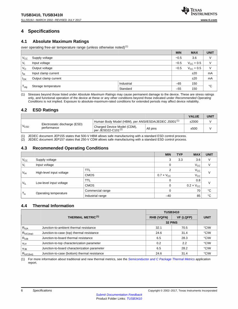
4.6.2 Reset TimingThere are three requirements for the reset signal timing. First, the minimum reset pulse duration is 100 μs.At power up, this time is measured from the time the power ramps up to 90% of the nominal VCC until thereset signal exceeds 1.2 V. The second requirement is that the clock must be valid during the last 60 µs ofthe reset window. The third requirement is that, according to the USB specification, the device must beready to respond to the host within 100 ms. This means that within the 100-ms window, the device mustcome out of reset, load any pertinent data from the I2C EEPROM device, and transfer execution to theapplication firmware if any is present. Because the latter two events can require significant time, theamount of which can change from system to system, TI recommends having the device come out of resetwithin 30 ms, leaving 70 ms for the other events to complete. This means the reset signal must rise to1.8 V within 30 ms.
These requirements are depicted in Figure 4-1. When using a 12-MHz crystal, the clock signal may takeseveral milliseconds to ramp up and become valid after power up. Therefore, the reset window may needto be elongated up to 10 ms or more to ensure that there is a 60-µs overlap with a valid clock.
Figure 4-1. Reset Timing
2400 4800 7200 9600 19200 38400 57600 115200 230400 460800 921600 10.48
10.49
10.5
10.51
10.52
10.53
10.54
10.55
10.56
10.57
10.58
10.59
10.6
10.61
10.62
10.63
10.64
Sup
ply
Cur
rent
(m
A)
Baud Rate (bps)
3.6 V
C006
2400 4800 7200 9600 19200 38400 57600 115200 230400 460800 921600 8.7
8.72
8.74
8.76
8.78
8.8
8.82
8.84
8.86
8.88
8.9
8.92
8.94
Sup
ply
Cur
rent
(m
A)
Baud Rate (bps)
3 V
C004
2400 4800 7200 9600 19200 38400 57600 115200 230400 460800 921600 9.64
9.65
9.66
9.67
9.68
9.69
9.7
9.71
9.72
9.73
9.74
9.75
9.76
9.77
9.78
9.79
9.8
Sup
ply
Cur
rent
(m
A)
Baud Rate (bps)
3.3 V
C005
9
TUSB3410, TUSB3410Iwww.ti.com SLLS519J –MARCH 2002–REVISED JULY 2017
Submit Documentation FeedbackProduct Folder Links: TUSB3410
SpecificationsCopyright © 2002–2017, Texas Instruments Incorporated
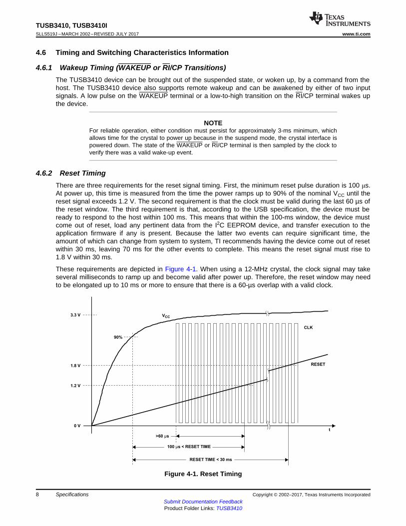
4.7 Typical Characteristics
Figure 4-2. Supply Current at 3 V Figure 4-3. Supply Current at 3.3 V
Figure 4-4. Supply Current at 3.6 V
Host
(PC or On-The-Go
Dual-Role Device)
Out
USB
In
TUSB3410
SOUT
SIN
Legacy
Serial
Peripheral
10
TUSB3410, TUSB3410ISLLS519J –MARCH 2002–REVISED JULY 2017 www.ti.com
Submit Documentation FeedbackProduct Folder Links: TUSB3410
Detailed Description Copyright © 2002–2017, Texas Instruments Incorporated
5 Detailed Description
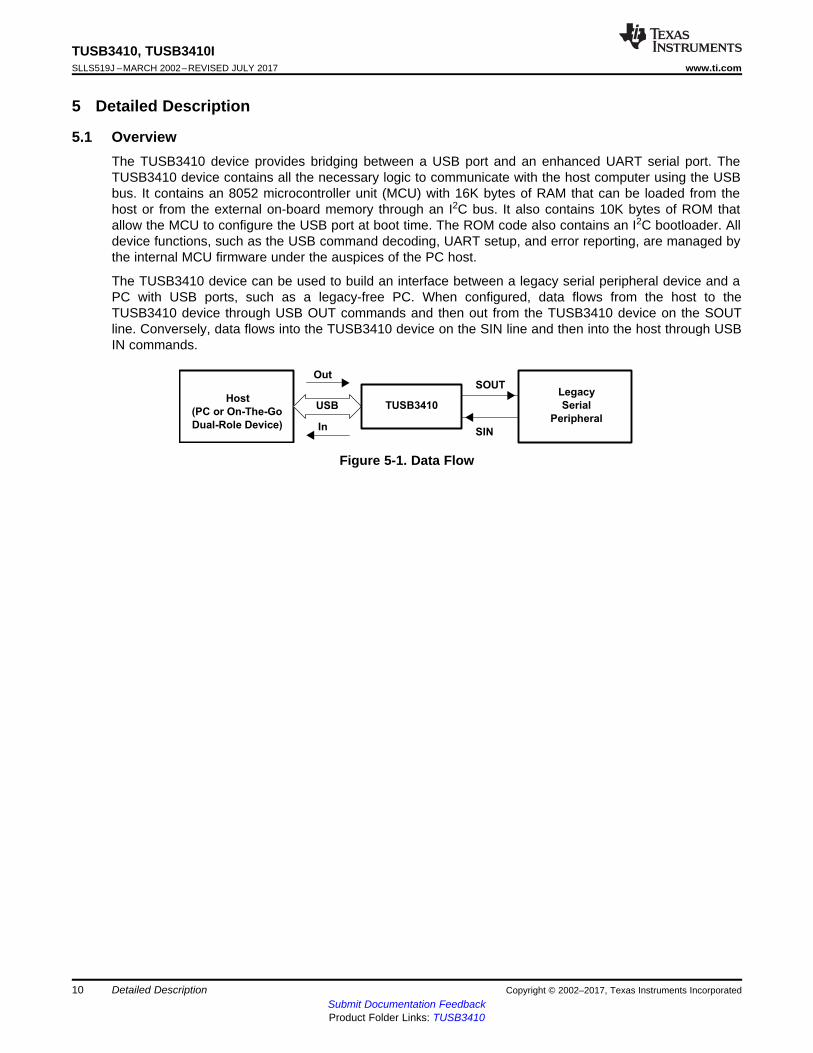
5.1 OverviewThe TUSB3410 device provides bridging between a USB port and an enhanced UART serial port. TheTUSB3410 device contains all the necessary logic to communicate with the host computer using the USBbus. It contains an 8052 microcontroller unit (MCU) with 16K bytes of RAM that can be loaded from thehost or from the external on-board memory through an I2C bus. It also contains 10K bytes of ROM thatallow the MCU to configure the USB port at boot time. The ROM code also contains an I2C bootloader. Alldevice functions, such as the USB command decoding, UART setup, and error reporting, are managed bythe internal MCU firmware under the auspices of the PC host.
The TUSB3410 device can be used to build an interface between a legacy serial peripheral device and aPC with USB ports, such as a legacy-free PC. When configured, data flows from the host to theTUSB3410 device through USB OUT commands and then out from the TUSB3410 device on the SOUTline. Conversely, data flows into the TUSB3410 device on the SIN line and then into the host through USBIN commands.
Figure 5-1. Data Flow
12 MHz
Clock
Oscillator
DP, DM
PLL and
Dividers
USB
TxR
24 MHz
10K 8×
ROM
8052
Core
8 8
8
16-Bit
Timers
16K 8×
RAM
82K × 8
SRAM
8 4
Port 3
8
P3.4
P3.3
P3.1
P3.0
USB
Serial
Interface
Engine
CPU-I/F8
Suspend/
Resume
8UBM
8
USB Buffer
Manager
8
8
SIN
I C2
Controller
DMA-1
DMA-3
UART−1
SOUT
I2C Bus
RTSCTSDTRDSR
TDM
Control
Logic IR
Encoder MUX
SOUT/IR_SOUT
IRM Decoder
SIN/IR_SIN
UX
2 ×
Copyright © 2017, Texas Instruments Incorporated
11
TUSB3410, TUSB3410Iwww.ti.com SLLS519J –MARCH 2002–REVISED JULY 2017
Submit Documentation FeedbackProduct Folder Links: TUSB3410
Detailed DescriptionCopyright © 2002–2017, Texas Instruments Incorporated
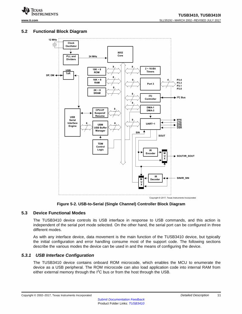
5.2 Functional Block Diagram
Figure 5-2. USB-to-Serial (Single Channel) Controller Block Diagram
5.3 Device Functional ModesThe TUSB3410 device controls its USB interface in response to USB commands, and this action isindependent of the serial port mode selected. On the other hand, the serial port can be configured in threedifferent modes.
As with any interface device, data movement is the main function of the TUSB3410 device, but typicallythe initial configuration and error handling consume most of the support code. The following sectionsdescribe the various modes the device can be used in and the means of configuring the device.
5.3.1 USB Interface ConfigurationThe TUSB3410 device contains onboard ROM microcode, which enables the MCU to enumerate thedevice as a USB peripheral. The ROM microcode can also load application code into internal RAM fromeither external memory through the I2C bus or from the host through the USB.
12
TUSB3410, TUSB3410ISLLS519J –MARCH 2002–REVISED JULY 2017 www.ti.com
Submit Documentation FeedbackProduct Folder Links: TUSB3410
Detailed Description Copyright © 2002–2017, Texas Instruments Incorporated
5.3.1.1 External Memory Case
After reset, the TUSB3410 device is disconnected from the USB. Bit 7 (CONT) in the USBCTL register(see Section 5.5.5.4) is cleared. The TUSB3410 device checks the I2C port for the existence of valid code;if it finds valid code, then the device uploads the code from the external memory device into the RAMprogram space. When loaded, the TUSB3410 device connects to the USB by setting the CONT bit; then,enumeration and configuration are performed. This is the most likely use of the device.
5.3.1.2 Host Download Case
If the valid code is not found at the I2C port, then the TUSB3410 device connects to the USB by setting bit7 (CONT) in the USBCTL register (see Section 5.5.5.4), and then an enumeration and defaultconfiguration are performed. The host can download additional microcode into RAM to tailor theapplication. Then, the MCU causes a disconnect and reconnect by clearing and setting the CONT bit,which causes the TUSB3410 device to be re-enumerated with a new configuration.
5.3.2 USB Data MovementFrom the USB perspective, the TUSB3410 device looks like a USB peripheral device. It uses endpointzero as its control endpoint, as do all USB peripherals. It also configures up to three input and three outputendpoints, although most applications use one bulk input endpoint for data in, one bulk output endpoint fordata out, and one interrupt endpoint for status updates. The USB configuration likely remains the sameregardless of the serial port configuration.
Most data is moved from the USB side to the UART side and from the UART side to the USB side usingon-chip DMA transfers. Some special cases may use programmed I/O under control of the MCU.
5.3.3 Serial Port SetupThe serial port requires a few control registers to be written to configure its operation. This configurationlikely remains the same regardless of the data mode used. These registers include the line control registerthat controls the serial word format and the divisor registers that control the baud rate.
These registers are usually controlled by the host application.
5.3.4 Serial Port Data ModesThe serial port can be configured in three different, although similar, data modes: the RS-232 data mode,the RS-485 data mode, and the IrDA data mode. Similar to the USB mode, when configured for a specificapplication, it is unlikely that the mode would be changed. The different modes affect the timing of theserial input and output or the use of the control signals. However, the basic serial-to-parallel conversion ofthe receiver and parallel-to-serial conversion of the transmitter remain the same in all modes. Somefeatures are available in all modes, but are only applicable in certain modes. For instance, software flowcontrol through Xoff/Xon characters can be used in all modes, but would usually only be used in RS-232or IrDA mode because the RS-485 mode is half-duplex communication. Similarly, hardware flow controlthrough RTS/CTS (or DTR/DSR) handshaking is available in RS-232 or IrDA mode. However, this wouldprobably be used only in RS-232 mode, because in IrDA mode only the SIN and SOUT paths are opticallycoupled.
5.3.4.1 RS-232 Data Mode
The default mode is called the RS-232 mode and is typically used for full duplex communication on SOUTand SIN. In this mode, the modem control outputs (RTS and DTR) communicate to a modem or aregeneral outputs. The modem control inputs (CTS, DSR, DCD, and RI/CP) communicate to a modem orare general inputs. Alternatively, RTS and CTS (or DTR and DSR) can throttle the data flow on SOUT andSIN to prevent receive FIFO overruns. Finally, software flow control through Xoff/Xon characters can beused for the same purpose (see Section 5.2).
This mode represents the most general-purpose applications, and the other modes are subsets of thismode.
13
TUSB3410, TUSB3410Iwww.ti.com SLLS519J –MARCH 2002–REVISED JULY 2017
Submit Documentation FeedbackProduct Folder Links: TUSB3410
Detailed DescriptionCopyright © 2002–2017, Texas Instruments Incorporated
5.3.4.2 RS-485 Data Mode
The RS-485 mode is very similar to the RS-232 mode in that the SOUT and SIN formats remain the same.Because RS-485 is a bus architecture, it is inherently a single duplex communication system. TheTUSB3410 device in RS-485 mode controls the RTS and DTR signals such that either can enable an RS-485 driver or RS-485 receiver. When in RS-485 mode, the enable signals for transmitting areautomatically asserted whenever the DMA is set up for outbound data.
NOTEThe receiver can be left enabled while the driver is enabled to allow an echo if desired, butwhen receive data is expected, the driver must be disabled. This precludes use of hardwareflow control, because this is a half-duplex operation, it would not be effective. Software flowcontrol is supported, but may be of limited value.
The RS-485 mode is enabled by setting bit 7 (485E) in the FCRL register (see Section 5.5.7.4), and bit 1(RCVE) in the MCR register (see Section 5.5.7.6) allows the receiver to eavesdrop while in the RS-485mode.
5.3.4.3 IrDA Data Mode
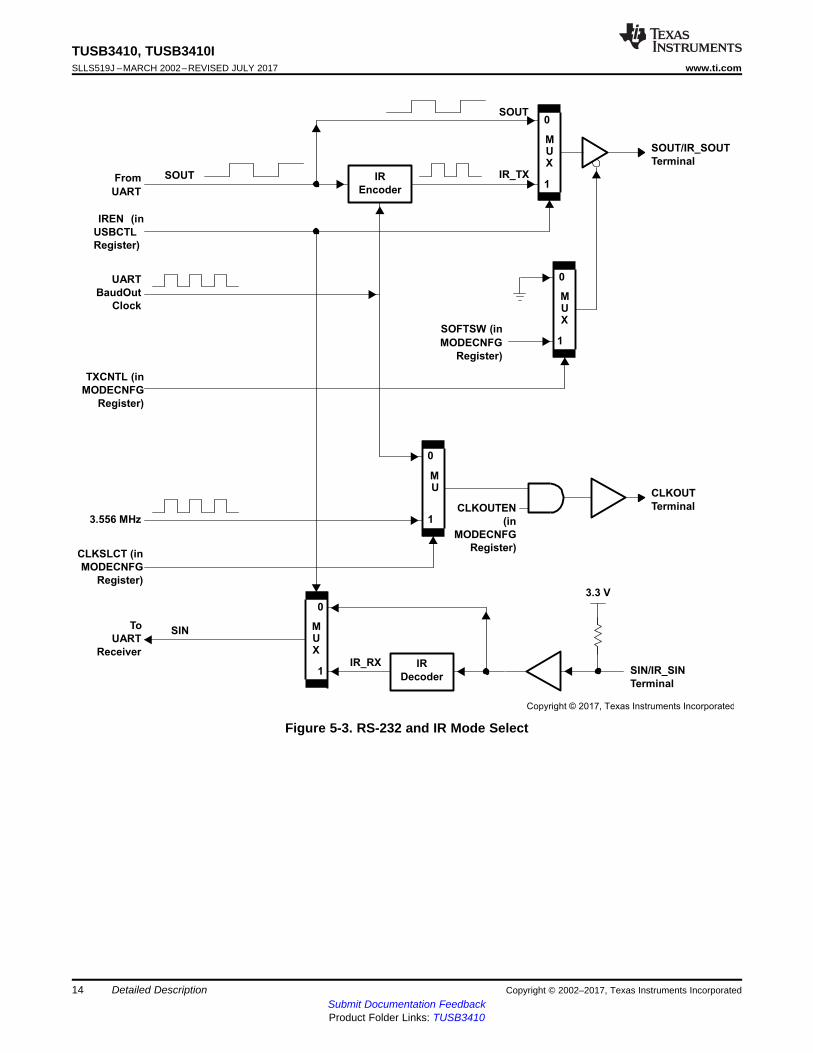
The IrDA mode encodes SOUT and decodes SIN in the manner prescribed by the IrDA standard, up to115.2 kbps. Connection to an external IrDA transceiver is required. Communications is usually full duplex.Generally, in an IrDA system, only the SOUT and SIN paths are connected so hardware flow control isusually not an option. Software flow control is supported (see Section 5.2).
The IrDA mode is enabled by setting bit 6 (IREN) in the USBCTL register (see Section 5.5.5.4).
The IR encoder and decoder circuitry work with the UART to change the serial bit stream into a series ofpulses and back again. For every zero bit in the outbound serial stream, the encoder sends a low-to-high-to-low pulse with the duration of 3/16 of a bit frame at the middle of the bit time. For every one bit in theserial stream, the output remains low for the entire bit time.
The decoding process consists of receiving the signal from the IrDA receiver and converting it into a seriesof zeroes and ones. As the converse to the encoder, the decoder converts a pulse to a zero bit and thelack of a pulse to a one bit.
From
UART
SOUT IR
Encoder
SOUT0
MUX
IR_TX1
SOUT/IR_SOUT
Terminal
IREN (in
USBCTL
Register)
UART
BaudOut
Clock
0
MUX
SOFTSW (in
MODECNFG 1
Register)
TXCNTL (in
MODECNFG
Register)
3.556 MHz
CLKSLCT (in
MODECNFG
Register)
To
UART
Receiver
SIN
0
MUX
IR_RX1
0
MU
1
IR
Decoder
CLKOUTEN
(in
MODECNFG
Register)
3.3 V
CLKOUT
Terminal
SIN/IR_SIN
Terminal
Copyright © 2017, Texas Instruments Incorporated
14
TUSB3410, TUSB3410ISLLS519J –MARCH 2002–REVISED JULY 2017 www.ti.com
Submit Documentation FeedbackProduct Folder Links: TUSB3410
Detailed Description Copyright © 2002–2017, Texas Instruments Incorporated
Figure 5-3. RS-232 and IR Mode Select

12 MHzX1/CLKI
X2
RTS
SOUT
RS-485 Bus
DTR
USB-0DP
DMTUSB3410
SIN
RS-485
Transceiver
2-Bit Time 1-Bit Max
SOUT
DTR
RTS
Receiver is Disabled if RCVE = 0
Copyright © 2017, Texas Instruments Incorporated
12 MHzX1/CLKI
X2
DTR
RTS
Transceivers
DB9
Connector
4
7
USB-0
RI/CP
DCD
DSR
CTS
DPSOUT
DMSIN
1
Serial Port
6
8
32
TUSB3410
P3.0
P3.1
P3.3
P3.4
GPIO Terminals for
Other Onboard
Control Function
Copyright © 2017, Texas Instruments Incorporated
15
TUSB3410, TUSB3410Iwww.ti.com SLLS519J –MARCH 2002–REVISED JULY 2017
Submit Documentation FeedbackProduct Folder Links: TUSB3410
Detailed DescriptionCopyright © 2002–2017, Texas Instruments Incorporated
Figure 5-4. USB-to-Serial Implementation (RS-232)
Figure 5-5. RS-485 Bus Implementation

16
TUSB3410, TUSB3410ISLLS519J –MARCH 2002–REVISED JULY 2017 www.ti.com
Submit Documentation FeedbackProduct Folder Links: TUSB3410
Detailed Description Copyright © 2002–2017, Texas Instruments Incorporated
5.4 Processor Subsystems
5.4.1 DMA Controller
5.4.1.1 Bulk Data I/O Using the EDB
The UBM (USB buffer manager) and the DMAC (DMA controller) access the EDB to fetch bufferparameters for IN and OUT transactions (IN and OUT are with respect to host). In this discussion, it isassumed that:• The MCU initialized the EDBs• DMA-continuous mode is being used• Double buffering is being used• The X/Y toggle is controlled by the UBM
5.4.1.1.1 IN Transaction (TUSB3410 to Host)1. The MCU initializes the IEDB (64-byte packet, and double buffering is used) and the following DMA
registers:– DMACSR3: Defines the transaction time-out value.– DMACDR3: Defines the IEDB being used and the DMA mode of operation (continuous mode).
Once this register is set with EN = 1, the transfer starts.2. The DMA transfers data from the UART to the X buffer. When a block of 64 bytes is transferred, the
DMA updates the byte count and sets NAK to 0 in the input endpoint byte count register (indicating tothe UBM that the X buffer is ready to be transferred to host). The UBM starts X-buffer transfer to hostusing the byte-count value in the input endpoint byte count register and toggles the X/Y bit. The DMAcontinues transferring data from a device to Y buffer. At the end of the block transfer, the DMA updatesthe byte count and sets NAK to 0 in the input endpoint byte count register (indicating to the UBM thatthe Y buffer is ready to be transferred to host). The DMA continues the transfer from the device tohost, alternating between X and Y buffers without MCU intervention.
3. Transfer termination: The DMA/UBM continues the data transfer, alternating between the X and Ybuffers. Termination of the transfer can happen under the following conditions:– Stop Transfer: The host notifies the MCU (through control-end-point) to stop the transfer. Under
this condition, the MCU sets bit 7 (EN) to 0 in the DMACDR register.– Partial Packet: The device receiver has no data to be transferred to host. Under this condition, the
byte-count value is less than 64 when the transaction timer time-out occurs. When the DMA detectsthis condition, it sets bit 1 (TXFT) to 1 and bit 0 (OVRUN) to 0 in the DMACSR3 register, updatesthe byte count and NAK bit in the input endpoint byte count register, and interrupts the MCU. TheUBM transfers the partial packet to host.
– Buffer Overrun: The host is busy, X and Y buffers are full (X-NAK = 0 and Y-NAK = 0), and theDMA cannot write to these buffers. The transaction time-out stops the DMA transfer, the DMA setsbit 1 (TXFT) to 1 and bit 0 (OVRUN) to 1 in the DMACSR3 register, and interrupts the MCU.
– UART Error Condition: When receiving from a UART, a receiver-error condition stops the DMAand sets bit 1 (TXFT) to 1 and bit 0 (OVRUN) to 0 in the DMACSR3 register, but the EN bit remainsset at 1. Therefore, the DMA does not interrupt the MCU. However, the UART generates a statusinterrupt, notifying the MCU that an error condition has occurred.
17
TUSB3410, TUSB3410Iwww.ti.com SLLS519J –MARCH 2002–REVISED JULY 2017
Submit Documentation FeedbackProduct Folder Links: TUSB3410
Detailed DescriptionCopyright © 2002–2017, Texas Instruments Incorporated
5.4.1.1.2 OUT Transaction (Host to TUSB3410)1. The MCU initializes the OEDB (64-byte packet, and double buffering is used) and the following DMA
registers:– DMACSR1: Provides an indication of a partial packet.– DMACDR1: Defines the output endpoint being used, and the DMA mode of operation (continuous
mode). When the EN bit is set to 1 in this register, the transfer starts.2. The UBM transfers data from host to X buffer. When a block of 64 bytes is transferred, the UBM
updates the byte count and sets NAK to 1 in the output endpoint byte count register (indicating to DMAthat the X buffer is ready to be transferred to the UART). The DMA starts X buffer transfer using thebyte-count value in the output endpoint byte count register. The UBM continues transferring data fromhost to Y buffer. At the end of the block transfer, the UBM updates the byte count and sets NAK to 1 inthe output endpoint byte count register (indicating to DMA that the Y buffer is ready to be transferred todevice). The DMA continues the transfer from the X and Y buffers to the device, alternating between Xand Y buffers without MCU intervention.
3. Transfer termination: The DMA/UBM continues the data transfer alternating between X and Y buffers.The termination of the transfer can happen under the following conditions:– Stop Transfer: The host notifies the MCU (through control-end point) to stop the transfer. Under
this condition, the MCU sets EN to 0 in the DMACDR1 register.– Partial Packet: UBM receives a partial packet from host. Under this condition, the byte-count value
is less than 64. When the DMA detects this condition, it transfers the partial packet to the device,sets PPKT to 1, updates NAK to 0 in the output endpoint byte count register and interrupts MCU.
64-Byte
Y-Buffer
64-Byte
X-Buffer
DMA
DMACDR3
Receiver
Halt on Error or Time-Out
RDR: 32-Byte FIFO
4 8
RTS/DTR = 1
SIN
Host
USB
Buffer
Manager
X/Y
Xoff/Xon
or Xoff Transmitted
RTS/DTR = 0
or Xon Transmitted
64-Byte
Y-Buffer
64-Byte
X-Buffer
CTS/DTR = 1/0
Pause/Run
DMA
DMACDR1
TDR
SOUT
Copyright © 2017, Texas Instruments Incorporated
18
TUSB3410, TUSB3410ISLLS519J –MARCH 2002–REVISED JULY 2017 www.ti.com
Submit Documentation FeedbackProduct Folder Links: TUSB3410
Detailed Description Copyright © 2002–2017, Texas Instruments Incorporated
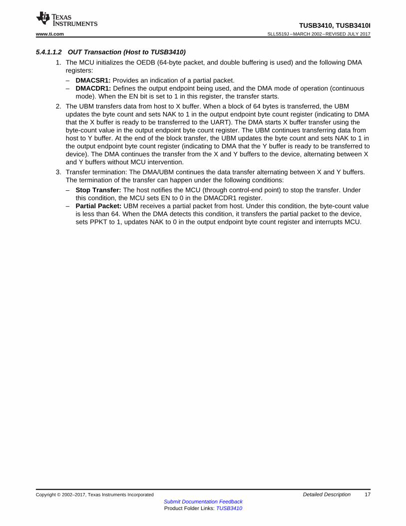
5.4.2 UART
5.4.2.1 UART Data Transfer
Figure 5-6 illustrates the data transfer between the UART and the host using the DMA controller and theUSB buffer manager (UBM). A buffer of 512 bytes is reserved for buffering the UART channel (transmitand receive buffers). The UART channel has 64 bytes of double-buffer space (X and Y buffer). When theDMA writes to the X buffer, the UBM reads from the Y buffer. Similarly, when the DMA reads from the Xbuffer, the UBM writes to the Y buffer. The DMA channel is configured to operate in the continuous mode(by setting bit 5 (CNT) in the DMACDR registers = 1). Once the MCU enables the DMA, data transfertoggles between the UMB and the DMA without MCU intervention. See Section 5.4.1.1.1 for DMAtransfer-termination condition.
5.4.2.1.1 Receiver Data Flow
The UART receiver has a 32-byte FIFO. The receiver FIFO has two trigger levels. One is the high-levelmark (HALT), which is set to 12 bytes, and the other is the low-level mark (RESUME), which is set to 4bytes. When the HALT mark is reached, either the RTS terminal goes high or Xoff is transmitted(depending on the auto setting). When the FIFO reaches the RESUME mark, then either the RTS terminalgoes low or Xon is transmitted.
Figure 5-6. Receiver and Transmitter Data Flow

TUSB3410
SIN
RTS
SOUT
CTS
External Device
SOUT
CTS
SIN
RTS
Copyright © 2017, Texas Instruments Incorporated
19
TUSB3410, TUSB3410Iwww.ti.com SLLS519J –MARCH 2002–REVISED JULY 2017
Submit Documentation FeedbackProduct Folder Links: TUSB3410
Detailed DescriptionCopyright © 2002–2017, Texas Instruments Incorporated
5.4.2.1.2 Hardware Flow Control
Figure 5-7 illustrates the connection necessary to achieve hardware flow control. The CTS and RTSsignals are provided for this purpose. Auto CTS and auto RTS (and Xon/Xoff) can be enabled anddisabled independently by programming the UART flow control register (FCRL).
Figure 5-7. Auto Flow Control Interconnect
5.4.2.1.3 Auto RTS (Receiver Control)
In this mode, the RTS output terminal signals the receiver-FIFO status to an external device. The RTSoutput signal is controlled by the high- and low-level marks of the FIFO. When the high-level mark isreached, RTS goes high, signaling to an external sending device to halt its transfer. Conversely, when thelow-level mark is reached, RTS goes low, signaling to an external sending device to resume its transfer.
Data transfer from the FIFO to the X and Y buffer is performed by the DMA controller. SeeSection 5.4.1.1.1 for DMA transfer-termination condition.
5.4.2.1.4 Auto CTS (Transmitter Control)
In this mode, the CTS input terminal controls the transfer from internal buffer (X or Y) to the TDR. Whenthe DMA controller transfers data from the Y buffer to the TDR and the CTS input terminal goes high, theDMA controller is suspended until CTS goes low. Meanwhile, the UBM is transferring data from the host tothe X buffer. When CTS goes low, the DMA resumes the transfer. Data transfer continues alternatingbetween the X and Y buffers, without MCU intervention. See Section 5.4.1.1.2 for DMA transfer-termination condition.
5.4.2.1.5 Xon/Xoff Receiver Flow Control
To enable Xon/Xoff flow control, certain bits within the modem control register must be set as follows:MCR bit 5 = 1 and MCR bits 6 and 7 = 00. In this mode, the Xon/Xoff bytes are transmitted to an externalsending device to control the transmission of the device. When the high-level mark (of the FIFO) isreached, the Xoff byte is transmitted, signaling to an external sending device to halt its transfer.Conversely, when the low-level mark is reached, the Xon byte is transmitted, signaling to an externalsending device to resume its transfer. The data transfer from the FIFO to X and Y buffer is performed bythe DMA controller.
5.4.2.1.6 Xon/Xoff Transmit Flow Control
To enable Xon/Xoff flow control, certain bits within the modem control register must be set as follows:MCR bit 5 = 1 and MCR bits 6 and 7 = 00. In this mode, the incoming data are compared to the XON andXOFF registers. If a match to XOFF is detected, the DMA is paused. If a match to XON is detected, theDMA resumes. Meanwhile, the UBM is transferring data from the host to the X-buffer. The MCU does notswitch the buffers unless the Y buffer is empty and the X-buffer is full. When Xon is detected, the DMAresumes the transfer.
20
TUSB3410, TUSB3410ISLLS519J –MARCH 2002–REVISED JULY 2017 www.ti.com
Submit Documentation FeedbackProduct Folder Links: TUSB3410
Detailed Description Copyright © 2002–2017, Texas Instruments Incorporated
5.4.3 I2C Port
5.4.3.1 Random-Read Operation
A random read requires a dummy byte-write sequence to load in the data word address. Once the device-address word and the data-word address are clocked out and acknowledged by the device, the MCUstarts a current-address sequence. The following describes the sequence of events to accomplish thistransaction.
5.4.3.1.1 Device Address + EPROM [High Byte]1. The MCU clears bit 1 (SRD) within the I2CSTA register. This forces the I2C controller not to generate a
stop condition after the contents of the I2CDAI register are received.2. The MCU clears bit 0 (SWR) within the I2CSTA register. This forces the I2C controller not to generate
a stop condition after the contents of the I2CDAO register are transmitted.3. The MCU writes the device address (bit 0 (R/W) = 0) to the I2CADR register (write operation)4. The MCU writes the high byte of the EEPROM address into the I2CDAO register (this starts the
transfer on the SDA line).5. Bit 3 (TXE) in the I2CSTA register is automatically cleared (indicates busy) by writing data to the
I2CDAO register.6. The contents of the I2CADR register are transmitted to EEPROM (preceded by start condition on
SDA).7. The contents of the I2CDAO register are transmitted to EEPROM (EPROM address).8. Bit 3 (TXE) in the I2CSTA register is set and interrupts the MCU, indicating that the I2CDAO register
has been transmitted.9. A stop condition is not generated.
5.4.3.1.2 EPROM [Low Byte]1. The MCU writes the low byte of the EEPROM address into the I2CDAO register.2. Bit 3 (TXE) in the I2CSTA register is automatically cleared (indicates busy) by writing to the I2CDAO
register.3. The contents of the I2CDAO register are transmitted to the device (EEPROM address).4. Bit 3 (TXE) in the I2CSTA register is set and interrupts the MCU, indicating that the I2CDAO register
has been transmitted.5. This completes the dummy write operation. At this point, the EEPROM address is set and the MCU
can do either a single- or a sequential-read operation.
5.4.3.2 Current-Address Read Operation
When the EEPROM address is set, the MCU can read a single byte by executing the following steps:1. The MCU sets bit 1 (SRD) in the I2CSTA register to 1. This forces the I2C controller to generate a stop
condition after the I2CDAI-register contents are received.2. The MCU writes the device address (bit 0 (R/W) = 1) to the I2CADR register (read operation).3. The MCU writes a dummy byte to the I2CDAO register (this starts the transfer on SDA line).4. Bit 7 (RXF) in the I2CSTA register is cleared (RX is empty).5. The contents of the I2CADR register are transmitted to the device (preceded by start condition on
SDA).6. The data from EEPROM are latched into the I2CDAI register (stop condition is transmitted).7. Bit 7 (RXF) in the I2CSTA register is set and interrupts the MCU, indicating that the data are available.8. The MCU reads the I2CDAI register. This clears bit 7 (RXF) in the I2CSTA register.
21
TUSB3410, TUSB3410Iwww.ti.com SLLS519J –MARCH 2002–REVISED JULY 2017
Submit Documentation FeedbackProduct Folder Links: TUSB3410
Detailed DescriptionCopyright © 2002–2017, Texas Instruments Incorporated
5.4.3.3 Sequential-Read Operation
When the EEPROM address is set, the MCU can execute a sequential read operation by executing thefollowing steps (this example illustrates a 32-byte sequential read):
5.4.3.3.1 Device Address1. The MCU clears bit 1 (SRD) in the I2CSTA register. This forces the I2C controller to not generate a
stop condition after the I2CDAI register contents are received.2. The MCU writes the device address (bit 0 (R/W) = 1) to the I2CADR register (read operation).3. The MCU writes a dummy byte to the I2CDAO register (this starts the transfer on the SDA line).4. Bit 7 (RXF) in the I2CSTA register is cleared (RX is empty).5. The contents of the I2CADR register are transmitted to the device (preceded by start condition on
SDA).
5.4.3.3.2 N-Byte Read (31 Bytes)1. The data from the device is latched into the I2CDAI register (stop condition is not transmitted).2. Bit 7 (RXF) in the I2CSTA register is set and interrupts the MCU, indicating that data is available.3. The MCU reads the I2CDAI register. This clears bit 7 (RXF) in the I2CSTA register.4. This operation repeats 31 times.
5.4.3.3.3 Last-Byte Read (Byte 32)1. MCU sets bit 1 (SRD) in the I2STA register to 1. This forces the I2C controller to generate a stop
condition after the I2CDAI register contents are received.2. The data from the device is latched into the I2CDAI register (stop condition is transmitted).3. Bit 7 (RXF) in the I2CSTA register is set and interrupts the MCU, indicating that data is available.4. The MCU reads the I2CDAI register. This clears bit 7 (RXF) in the I2CSTA register.
5.4.3.4 Byte-Write Operation
The byte-write operation involves three phases: device address + EPROM [high byte] phase, EPROM [lowbyte] phase, and EPROM [DATA] phase. The following describes the sequence of events to accomplishthe byte-write transaction.
5.4.3.4.1 Device Address + EPROM [High Byte]1. The MCU sets clears the SWR bit in the I2CSTA register. This forces the I2C controller to not generate
a stop condition after the contents of the I2CDAO register are transmitted.2. The MCU writes the device address (bit 0 (R/W) = 0) to the I2CADR register (write operation).3. The MCU writes the high byte of the EEPROM address into the I2CDAO register (this starts the
transfer on the SDA line).4. Bit 3 (TXE) in the I2CSTA register is cleared (indicates busy).5. The contents of the I2CADR register are transmitted to the device (preceded by start condition on
SDA).6. The contents of the I2CDAO register are transmitted to the device (EEPROM high address).7. Bit 3 (TXE) in the I2CSTA register is set and interrupts the MCU, indicating that the I2CDAO register
contents have been transmitted.

22
TUSB3410, TUSB3410ISLLS519J –MARCH 2002–REVISED JULY 2017 www.ti.com
Submit Documentation FeedbackProduct Folder Links: TUSB3410
Detailed Description Copyright © 2002–2017, Texas Instruments Incorporated
5.4.3.4.2 EPROM [Low Byte]1. The MCU writes the low byte of the EEPROM address into the I2CDAO register.2. Bit 3 (TXE) in the I2CSTA register is cleared (indicating busy).3. The contents of the I2CDAO register are transmitted to the device (EEPROM address).4. Bit 3 (TXE) in the I2CSTA register is set and interrupts the MCU, indicating that the I2CDAO register
contents have been transmitted.
5.4.3.4.3 EPROM [DATA]1. The MCU sets bit 0 (SWR) in the I2CSTA register. This forces the I2C controller to generate a stop
condition after the contents of the I2CDAO register are transmitted.2. The data to be written to the EPROM is written by the MCU into the I2CDAO register.3. Bit 3 (TXE) in the I2CSTA register is cleared (indicates busy).4. The contents of the I2CDAO register are transmitted to the device (EEPROM data).5. Bit 3 (TXE) in the I2CSTA register is set and interrupts the MCU, indicating that the I2CDAO register
contents have been transmitted.6. The I2C controller generates a stop condition after the contents of the I2CDAO register are transmitted.
5.4.3.5 Page-Write Operation
The page-write operation is initiated in the same way as byte write, with the exception that a stopcondition is not generated after the first EPROM [DATA] is transmitted. The following describes thesequence of writing 32 bytes in page mode.
5.4.3.5.1 Device Address + EPROM [High Byte]1. The MCU clears bit 0 (SWR) in the I2CSTA register. This forces the I2C controller to not generate a
stop condition after the contents of the I2CDAO register are transmitted.2. The MCU writes the device address (bit 0 (R/W) = 0) to the I2CADR register (write operation).3. The MCU writes the high byte of the EEPROM address into the I2CDAO register.4. Bit 3 (TXE) in the I2CSTA register is cleared (indicating busy).5. The contents of the I2CADR register are transmitted to the device (preceded by start condition on
SDA).6. The contents of the I2CDAO register are transmitted to the device (EEPROM address).7. Bit 3 (TXE) in the I2CSTA register is set and interrupts the MCU, indicating that the I2CDAO register
contents have been transmitted.
5.4.3.5.2 EPROM [Low Byte]1. The MCU writes the low byte of the EEPROM address into the I2CDAO register.2. Bit 3 (TXE) in the I2CSTA register is cleared (indicates busy).3. The contents of the I2CDAO register are transmitted to the device (EEPROM address).4. Bit 3 (TXE) in the I2CSTA register is set and interrupts the MCU, indicating that the I2CDAO register
contents have been transmitted.

23
TUSB3410, TUSB3410Iwww.ti.com SLLS519J –MARCH 2002–REVISED JULY 2017
Submit Documentation FeedbackProduct Folder Links: TUSB3410
Detailed DescriptionCopyright © 2002–2017, Texas Instruments Incorporated
5.4.3.5.3 EPROM [DATA]—31 Bytes1. The data to be written to the EEPROM are written by the MCU into the I2CDAO register.2. Bit 3 (TXE) in the I2CSTA register is cleared (indicates busy).3. The contents of the I2CDAO register are transmitted to the device (EEPROM data).4. Bit 3 (TXE) in the I2CSTA register is set and interrupts the MCU, indicating that the I2CDAO register
contents have been transmitted.5. This operation repeats 31 times.
5.4.3.5.4 EPROM [DATA]—Last Byte1. The MCU sets bit 0 (SWR) in the I2CSTA register. This forces the I2C controller to generate a stop
condition after the contents of the I2CDAO register are transmitted.2. The MCU writes the last date byte to be written to the EEPROM, into the I2CDAO register.3. Bit 3 (TXE) in the I2CSTA register is cleared (indicates busy).4. The contents of the I2CDAO register are transmitted to EEPROM (EEPROM data).5. Bit 3 (TXE) in the I2CSTA register is set and interrupts the MCU, indicating that the I2CDAO register
contents have been transmitted.6. The I2C controller generates a stop condition after the contents of the I2CDAO register are transmitted.
Boot Mode (SDW = 0) Normal Mode (SDW = 1)
CODE XDATA CODE XDATA
0000h
27FFh
10K Boot ROM
(16K)
Read/Write
16K
Code RAM
Read Only
3FFFh
8000h
A7FFh
10K Boot ROM 10K Boot ROM
F800h
FF7Fh
2K Data 2K Data
FF80h
FFFFhMMR MMR
24
TUSB3410, TUSB3410ISLLS519J –MARCH 2002–REVISED JULY 2017 www.ti.com
Submit Documentation FeedbackProduct Folder Links: TUSB3410
Detailed Description Copyright © 2002–2017, Texas Instruments Incorporated
5.5 Memory
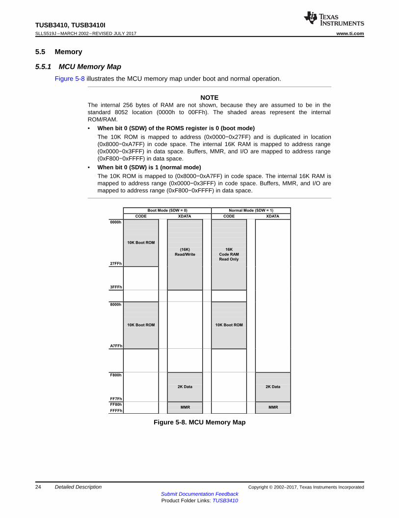
5.5.1 MCU Memory MapFigure 5-8 illustrates the MCU memory map under boot and normal operation.
NOTEThe internal 256 bytes of RAM are not shown, because they are assumed to be in thestandard 8052 location (0000h to 00FFh). The shaded areas represent the internalROM/RAM.• When bit 0 (SDW) of the ROMS register is 0 (boot mode)
The 10K ROM is mapped to address (0x0000−0x27FF) and is duplicated in location(0x8000−0xA7FF) in code space. The internal 16K RAM is mapped to address range(0x0000−0x3FFF) in data space. Buffers, MMR, and I/O are mapped to address range(0xF800−0xFFFF) in data space.
• When bit 0 (SDW) is 1 (normal mode)The 10K ROM is mapped to (0x8000−0xA7FF) in code space. The internal 16K RAM ismapped to address range (0x0000−0x3FFF) in code space. Buffers, MMR, and I/O aremapped to address range (0xF800−0xFFFF) in data space.
Figure 5-8. MCU Memory Map
25
TUSB3410, TUSB3410Iwww.ti.com SLLS519J –MARCH 2002–REVISED JULY 2017
Submit Documentation FeedbackProduct Folder Links: TUSB3410
Detailed DescriptionCopyright © 2002–2017, Texas Instruments Incorporated
5.5.2 Registers
5.5.2.1 Miscellaneous Registers
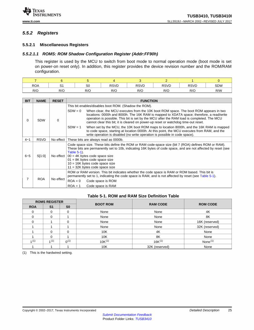
5.5.2.1.1 ROMS: ROM Shadow Configuration Register (Addr:FF90h)
This register is used by the MCU to switch from boot mode to normal operation mode (boot mode is seton power-on reset only). In addition, this register provides the device revision number and the ROM/RAMconfiguration.
7 6 5 4 3 2 1 0ROA S1 S0 RSVD RSVD RSVD RSVD SDWR/O R/O R/O R/O R/O R/O R/O R/W
BIT NAME RESET FUNCTION
0 SDW 0
This bit enables/disables boot ROM. (Shadow the ROM).SDW = 0 When clear, the MCU executes from the 10K boot ROM space. The boot ROM appears in two
locations: 0000h and 8000h. The 16K RAM is mapped to XDATA space; therefore, a read/writeoperation is possible. This bit is set by the MCU after the RAM load is completed. The MCUcannot clear this bit; it is cleared on power-up reset or watchdog time-out reset.
SDW = 1 When set by the MCU, the 10K boot ROM maps to location 8000h, and the 16K RAM is mappedto code space, starting at location 0000h. At this point, the MCU executes from RAM, and thewrite operation is disabled (no write operation is possible in code space).
4−1 RSVD No effect These bits are always read as 0000b.
6−5 S[1:0] No effect
Code space size. These bits define the ROM or RAM code-space size (bit 7 (ROA) defines ROM or RAM).These bits are permanently set to 10b, indicating 16K bytes of code space, and are not affected by reset (seeTable 5-1).00 = 4K bytes code space size01 = 8K bytes code space size10 = 16K bytes code space size11 = 32K bytes code space size
7 ROA No effect
ROM or RAM version. This bit indicates whether the code space is RAM or ROM based. This bit ispermanently set to 1, indicating the code space is RAM, and is not affected by reset (see Table 5-1).ROA = 0 Code space is ROMROA = 1 Code space is RAM
(1) This is the hardwired setting.
Table 5-1. ROM and RAM Size Definition TableROMS REGISTER
BOOT ROM RAM CODE ROM CODEROA S1 S0
0 0 0 None None 4K0 0 1 None None 8K0 1 0 None None 16K (reserved)1 1 1 None None 32K (reserved)1 0 0 10K 4K None1 0 1 10K 8K None
1 (1) 1 (1) 0 (1) 10K (1) 16K (1) None (1)
1 1 1 10K 32K (reserved) None

26
TUSB3410, TUSB3410ISLLS519J –MARCH 2002–REVISED JULY 2017 www.ti.com
Submit Documentation FeedbackProduct Folder Links: TUSB3410
Detailed Description Copyright © 2002–2017, Texas Instruments Incorporated
5.5.2.1.2 Boot Operation (MCU Firmware Loading)
Because the code space is in RAM (with the exception of the boot ROM), the TUSB3410 firmware mustbe loaded from an external source. Two sources are available for booting: one from an external serialEEPROM connected to the I2C bus and the other from the host through the USB. On device reset, bit 0(SDW) in the ROMS register (see Section 5.5.2.1.1) and bit 7 (CONT) in the USBCTL register (seeSection 5.5.5.4) are cleared. This configures the memory space to boot mode (see Table 5-3) and keepsthe device disconnected from the host. The first instruction is fetched from location 0000h (which is in the10K ROM). The 16K RAM is mapped to XDATA space (location 0000h). The MCU executes a read froman external EEPROM and tests whether it contains the code (by testing for boot signature). If it containsthe code, then the MCU reads from EEPROM and writes to the 16K RAM in XDATA space. If it does notcontain the code, then the MCU proceeds to boot from the USB.
When the code is loaded, the MCU sets the SDW bit to 1 in the ROMS register. This switches the memorymap to normal mode; that is, the 16K RAM is mapped to code space, and the MCU starts executing fromlocation 0000h. When the switch is done, the MCU sets the CONT bit to 1 in the USBCTL register. Thisconnects the device to the USB and results in normal USB device enumeration.
5.5.2.1.3 WDCSR: Watchdog Timer, Control, and Status Register (Addr:FF93h)
A watchdog timer (WDT) with 1-ms clock is provided. If this register is not accessed for a period of 128ms, then the WDT counter resets the MCU (see Figure 5-9). The watchdog timer is enabled by defaultand can be disabled by writing a pattern of 101010b into the WDD[5:0] bits. The 1-ms clock for thewatchdog timer is generated from the SOF pulses. Therefore, for the watchdog timer to count, bit 7(CONT) in the USBCTL register (see Section 5.5.5.4) must be set.
7 6 5 4 3 2 1 0WDD0 WDR WDD5 WDD4 WDD3 WDD2 WDD1 WDTR/W R/C R/W R/W R/W R/W R/W W/O
BIT NAME RESET FUNCTION
0 WDT 0MCU must write a 1 to this bit to prevent the watchdog timer from resetting the MCU. If the MCU doesnot write a 1 in a period of 128 ms, the watchdog timer resets the device. Writing a 0 has no effect onthe watchdog timer. (The watchdog timer is a 7-bit counter using a 1-ms CLK.) This bit is read as 0.
5−1 WDD[5:1] 00000These bits disable the watchdog timer. For the timer to be disabled these bits must be set to 10101band bit 7 (WDD0) must also be set to 0. If any other pattern is present, then the watchdog timer is inoperation.
6 WDR 0
Watchdog reset indication bit. This bit indicates if the reset occurred due to power-on reset or watchdogtimer reset.WDR = 0 A power-up reset occurredWDR = 1 A watchdog time-out reset occurred. To clear this bit, the MCU must write a 1. Writing a 0
has no effect.
7 WDD0 1 This bit is one of the six disable bits for the watchdog timer. This bit must be cleared in order for thewatchdog timer to be disabled.
27
TUSB3410, TUSB3410Iwww.ti.com SLLS519J –MARCH 2002–REVISED JULY 2017
Submit Documentation FeedbackProduct Folder Links: TUSB3410
Detailed DescriptionCopyright © 2002–2017, Texas Instruments Incorporated
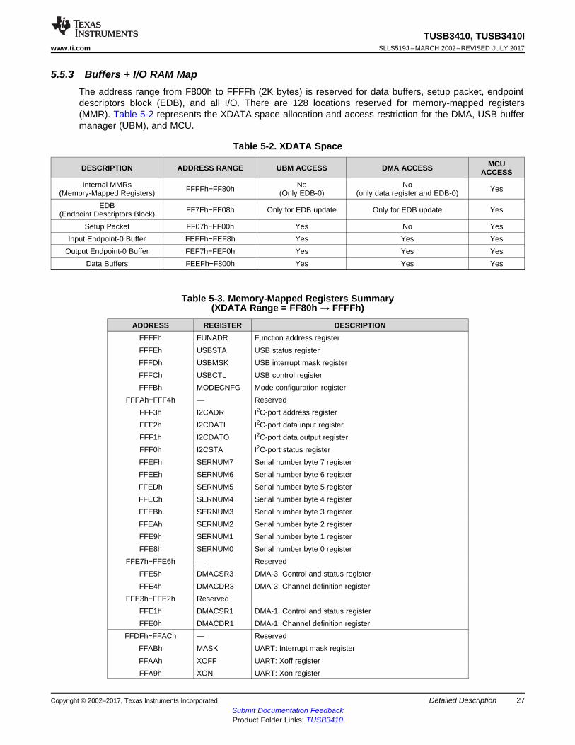
5.5.3 Buffers + I/O RAM MapThe address range from F800h to FFFFh (2K bytes) is reserved for data buffers, setup packet, endpointdescriptors block (EDB), and all I/O. There are 128 locations reserved for memory-mapped registers(MMR). Table 5-2 represents the XDATA space allocation and access restriction for the DMA, USB buffermanager (UBM), and MCU.
Table 5-2. XDATA Space
DESCRIPTION ADDRESS RANGE UBM ACCESS DMA ACCESS MCUACCESS
Internal MMRs(Memory-Mapped Registers) FFFFh−FF80h No
(Only EDB-0)No
(only data register and EDB-0) Yes
EDB(Endpoint Descriptors Block) FF7Fh−FF08h Only for EDB update Only for EDB update Yes
Setup Packet FF07h−FF00h Yes No YesInput Endpoint-0 Buffer FEFFh−FEF8h Yes Yes Yes
Output Endpoint-0 Buffer FEF7h−FEF0h Yes Yes YesData Buffers FEEFh−F800h Yes Yes Yes
Table 5-3. Memory-Mapped Registers Summary(XDATA Range = FF80h → FFFFh)
ADDRESS REGISTER DESCRIPTIONFFFFh FUNADR Function address registerFFFEh USBSTA USB status registerFFFDh USBMSK USB interrupt mask registerFFFCh USBCTL USB control registerFFFBh MODECNFG Mode configuration register
FFFAh−FFF4h — ReservedFFF3h I2CADR I2C-port address registerFFF2h I2CDATI I2C-port data input registerFFF1h I2CDATO I2C-port data output registerFFF0h I2CSTA I2C-port status registerFFEFh SERNUM7 Serial number byte 7 registerFFEEh SERNUM6 Serial number byte 6 registerFFEDh SERNUM5 Serial number byte 5 registerFFECh SERNUM4 Serial number byte 4 registerFFEBh SERNUM3 Serial number byte 3 registerFFEAh SERNUM2 Serial number byte 2 registerFFE9h SERNUM1 Serial number byte 1 registerFFE8h SERNUM0 Serial number byte 0 register
FFE7h−FFE6h — ReservedFFE5h DMACSR3 DMA-3: Control and status registerFFE4h DMACDR3 DMA-3: Channel definition register
FFE3h−FFE2h ReservedFFE1h DMACSR1 DMA-1: Control and status registerFFE0h DMACDR1 DMA-1: Channel definition register
FFDFh−FFACh — ReservedFFABh MASK UART: Interrupt mask registerFFAAh XOFF UART: Xoff registerFFA9h XON UART: Xon register

28
TUSB3410, TUSB3410ISLLS519J –MARCH 2002–REVISED JULY 2017 www.ti.com
Submit Documentation FeedbackProduct Folder Links: TUSB3410
Detailed Description Copyright © 2002–2017, Texas Instruments Incorporated
Table 5-3. Memory-Mapped Registers Summary(XDATA Range = FF80h → FFFFh) (continued)
ADDRESS REGISTER DESCRIPTIONFFA8h DLH UART: Divisor high-byte registerFFA7h DLL UART: Divisor low-byte registerFFA6h MSR UART: Modem status registerFFA5h LSR UART: Line status registerFFA4h MCR UART: Modem control registerFFA3h FCRL UART: Flow control registerFFA2h LCR UART: Line control registersFFA1h TDR UART: Transmitter data registersFFA0h RDR UART: Receiver data registersFF9Eh PUR_3 GPIO: Pullup register for port 3
FF9Dh−FF94h — ReservedFF93h WDCSR Watchdog timer control and status registerFF92h VECINT Vector interrupt registerFF91h — ReservedFF90h ROMS ROM shadow configuration register
FF8Fh−FF84h — ReservedFF83h OEPBCNT_0 Output endpoint_0: Byte count registerFF82h OEPCNFG_0 Output endpoint_0: Configuration registerFF81h IEPBCNT_0 Input endpoint_0: Byte count registerFF80h IEPCNFG_0 Input endpoint_0: Configuration register
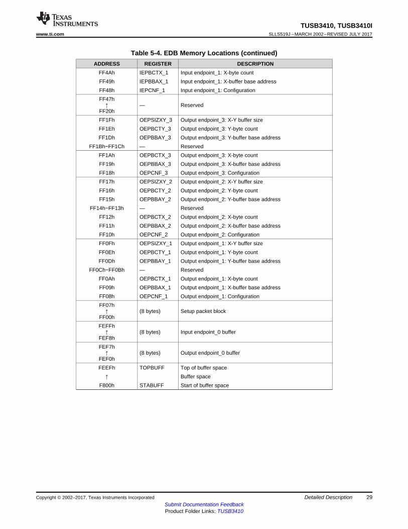
Table 5-4. EDB Memory Locations
ADDRESS REGISTER DESCRIPTIONFF7Fh−FF60h — Reserved
FF5Fh IEPSIZXY_3 Input endpoint_3: X-Y buffer sizeFF5Eh IEPBCTY_3 Input endpoint_3: Y-byte countFF5Dh IEPBBAY_3 Input endpoint_3: Y-buffer base addressFF5Ch — ReservedFF5Bh — ReservedFF5Ah IEPBCTX_3 Input endpoint_3: X-byte countFF59h IEPBBAX Input endpoint_3: X-buffer base addressFF58h IEPCNF_3 Input endpoint_3: ConfigurationFF57h IEPSIZXY_2v Input endpoint_2: X-Y buffer sizeFF56h IEPBCTY_2 Input endpoint_2: Y-byte countFF55h IEPBBAY_2 Input endpoint_2: Y-buffer base addressFF54h — ReservedFF53h — ReservedFF52h IEPBCTX_2 Input endpoint_2: X-byte countFF51h IEPBBAX_2 Input endpoint_2: X-buffer base addressFF50h IEPCNF_2 Input endpoint_2: ConfigurationFF4Fh IEPSIZXY_1 Input endpoint_1: X-Y buffer sizeFF4Eh IEPBCTY_1 Input endpoint_1: Y-byte countFF4Dh IEPBBAY_1 Input endpoint_1: Y-buffer base addressFF4Ch — ReservedFF4Bh — Reserved
29
TUSB3410, TUSB3410Iwww.ti.com SLLS519J –MARCH 2002–REVISED JULY 2017
Submit Documentation FeedbackProduct Folder Links: TUSB3410
Detailed DescriptionCopyright © 2002–2017, Texas Instruments Incorporated
Table 5-4. EDB Memory Locations (continued)ADDRESS REGISTER DESCRIPTION
FF4Ah IEPBCTX_1 Input endpoint_1: X-byte countFF49h IEPBBAX_1 Input endpoint_1: X-buffer base addressFF48h IEPCNF_1 Input endpoint_1: ConfigurationFF47h
↑FF20h
— Reserved
FF1Fh OEPSIZXY_3 Output endpoint_3: X-Y buffer sizeFF1Eh OEPBCTY_3 Output endpoint_3: Y-byte countFF1Dh OEPBBAY_3 Output endpoint_3: Y-buffer base address
FF1Bh−FF1Ch — ReservedFF1Ah OEPBCTX_3 Output endpoint_3: X-byte countFF19h OEPBBAX_3 Output endpoint_3: X-buffer base addressFF18h OEPCNF_3 Output endpoint_3: ConfigurationFF17h OEPSIZXY_2 Output endpoint_2: X-Y buffer sizeFF16h OEPBCTY_2 Output endpoint_2: Y-byte countFF15h OEPBBAY_2 Output endpoint_2: Y-buffer base address
FF14h−FF13h — ReservedFF12h OEPBCTX_2 Output endpoint_2: X-byte countFF11h OEPBBAX_2 Output endpoint_2: X-buffer base addressFF10h OEPCNF_2 Output endpoint_2: ConfigurationFF0Fh OEPSIZXY_1 Output endpoint_1: X-Y buffer sizeFF0Eh OEPBCTY_1 Output endpoint_1: Y-byte countFF0Dh OEPBBAY_1 Output endpoint_1: Y-buffer base address
FF0Ch−FF0Bh — ReservedFF0Ah OEPBCTX_1 Output endpoint_1: X-byte countFF09h OEPBBAX_1 Output endpoint_1: X-buffer base addressFF08h OEPCNF_1 Output endpoint_1: ConfigurationFF07h
↑FF00h
(8 bytes) Setup packet block
FEFFh↑
FEF8h(8 bytes) Input endpoint_0 buffer
FEF7h↑
FEF0h(8 bytes) Output endpoint_0 buffer
FEEFh TOPBUFF Top of buffer space↑ Buffer space
F800h STABUFF Start of buffer space
30
TUSB3410, TUSB3410ISLLS519J –MARCH 2002–REVISED JULY 2017 www.ti.com
Submit Documentation FeedbackProduct Folder Links: TUSB3410
Detailed Description Copyright © 2002–2017, Texas Instruments Incorporated
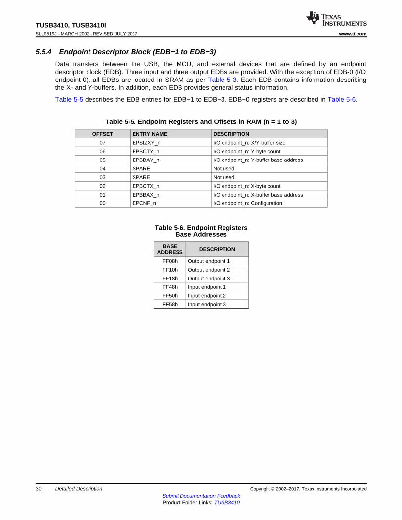
5.5.4 Endpoint Descriptor Block (EDB−1 to EDB−3)Data transfers between the USB, the MCU, and external devices that are defined by an endpointdescriptor block (EDB). Three input and three output EDBs are provided. With the exception of EDB-0 (I/Oendpoint-0), all EDBs are located in SRAM as per Table 5-3. Each EDB contains information describingthe X- and Y-buffers. In addition, each EDB provides general status information.
Table 5-5 describes the EDB entries for EDB−1 to EDB−3. EDB−0 registers are described in Table 5-6.
Table 5-5. Endpoint Registers and Offsets in RAM (n = 1 to 3)
OFFSET ENTRY NAME DESCRIPTION07 EPSIZXY_n I/O endpoint_n: X/Y-buffer size06 EPBCTY_n I/O endpoint_n: Y-byte count05 EPBBAY_n I/O endpoint_n: Y-buffer base address04 SPARE Not used03 SPARE Not used02 EPBCTX_n I/O endpoint_n: X-byte count01 EPBBAX_n I/O endpoint_n: X-buffer base address00 EPCNF_n I/O endpoint_n: Configuration
Table 5-6. Endpoint RegistersBase Addresses
BASEADDRESS DESCRIPTION
FF08h Output endpoint 1FF10h Output endpoint 2FF18h Output endpoint 3FF48h Input endpoint 1FF50h Input endpoint 2FF58h Input endpoint 3
31
TUSB3410, TUSB3410Iwww.ti.com SLLS519J –MARCH 2002–REVISED JULY 2017
Submit Documentation FeedbackProduct Folder Links: TUSB3410
Detailed DescriptionCopyright © 2002–2017, Texas Instruments Incorporated
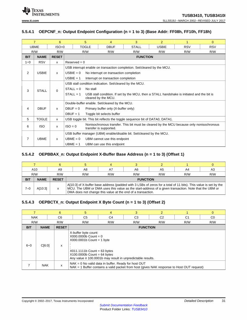
5.5.4.1 OEPCNF_n: Output Endpoint Configuration (n = 1 to 3) (Base Addr: FF08h, FF10h, FF18h)
7 6 5 4 3 2 1 0UBME ISO=0 TOGLE DBUF STALL USBIE RSV RSVR/W R/W R/W R/W R/W R/W R/W R/W
BIT NAME RESET FUNCTION1−0 RSV x Reserved = 0
2 USBIE xUSB interrupt enable on transaction completion. Set/cleared by the MCU.USBIE = 0 No interrupt on transaction completionUSBIE = 1 Interrupt on transaction completion
3 STALL 0
USB stall condition indication. Set/cleared by the MCU.STALL = 0 No stallSTALL = 1 USB stall condition. If set by the MCU, then a STALL handshake is initiated and the bit is
cleared by the MCU.
4 DBUF xDouble-buffer enable. Set/cleared by the MCU.DBUF = 0 Primary buffer only (X-buffer only)DBUF = 1 Toggle bit selects buffer
5 TOGLE x USB toggle bit. This bit reflects the toggle sequence bit of DATA0, DATA1.
6 ISO x ISO = 0 Nonisochronous transfer. This bit must be cleared by the MCU because only nonisochronoustransfer is supported.
7 UBME xUSB buffer manager (UBM) enable/disable bit. Set/cleared by the MCU.UBME = 0 UBM cannot use this endpointUBME = 1 UBM can use this endpoint
5.5.4.2 OEPBBAX_n: Output Endpoint X-Buffer Base Address (n = 1 to 3) (Offset 1)
7 6 5 4 3 2 1 0A10 A9 A8 A7 A6 A5 A4 A3R/W R/W R/W R/W R/W R/W R/W R/W
BIT NAME RESET FUNCTION
7–0 A[10:3] xA[10:3] of X-buffer base address (padded with 3 LSBs of zeros for a total of 11 bits). This value is set by theMCU. The UBM or DMA uses this value as the start-address of a given transaction. Note that the UBM orDMA does not change this value at the end of a transaction.
5.5.4.3 OEPBCTX_n: Output Endpoint X Byte Count (n = 1 to 3) (Offset 2)
7 6 5 4 3 2 1 0NAK C6 C5 C4 C3 C2 C1 C0R/W R/W R/W R/W R/W R/W R/W R/W
BIT NAME RESET FUNCTION
6−0 C[6:0] x
X-buffer byte count:X000.0000b Count = 0X000.0001b Count = 1 byte::X011.1111b Count = 63 bytesX100.0000b Count = 64 bytesAny value ≥ 100.0001b may result in unpredictable results.
7 NAK x NAK = 0 No valid data in buffer. Ready for host OUTNAK = 1 Buffer contains a valid packet from host (gives NAK response to Host OUT request)
32
TUSB3410, TUSB3410ISLLS519J –MARCH 2002–REVISED JULY 2017 www.ti.com
Submit Documentation FeedbackProduct Folder Links: TUSB3410
Detailed Description Copyright © 2002–2017, Texas Instruments Incorporated
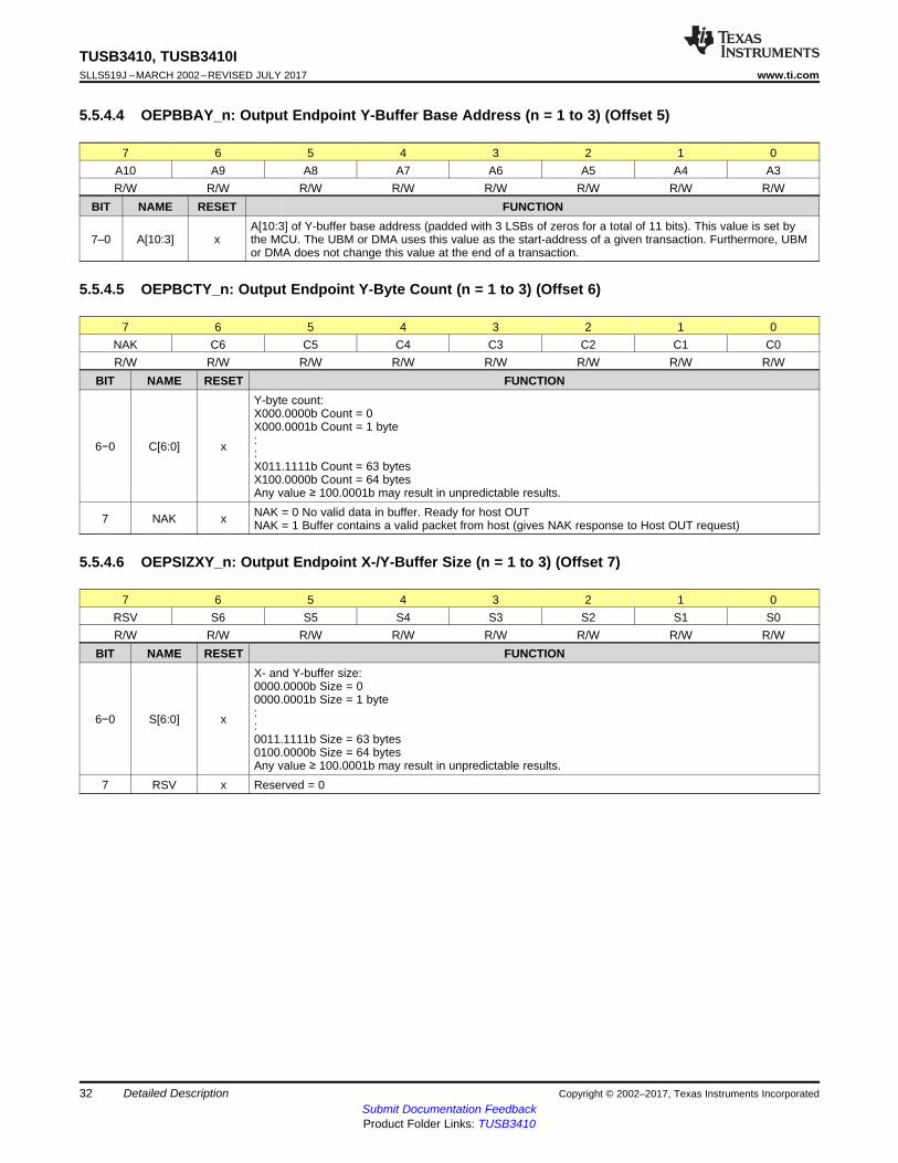
5.5.4.4 OEPBBAY_n: Output Endpoint Y-Buffer Base Address (n = 1 to 3) (Offset 5)
7 6 5 4 3 2 1 0A10 A9 A8 A7 A6 A5 A4 A3R/W R/W R/W R/W R/W R/W R/W R/W
BIT NAME RESET FUNCTION
7–0 A[10:3] xA[10:3] of Y-buffer base address (padded with 3 LSBs of zeros for a total of 11 bits). This value is set bythe MCU. The UBM or DMA uses this value as the start-address of a given transaction. Furthermore, UBMor DMA does not change this value at the end of a transaction.
5.5.4.5 OEPBCTY_n: Output Endpoint Y-Byte Count (n = 1 to 3) (Offset 6)
7 6 5 4 3 2 1 0NAK C6 C5 C4 C3 C2 C1 C0R/W R/W R/W R/W R/W R/W R/W R/W
BIT NAME RESET FUNCTION
6−0 C[6:0] x
Y-byte count:X000.0000b Count = 0X000.0001b Count = 1 byte::X011.1111b Count = 63 bytesX100.0000b Count = 64 bytesAny value ≥ 100.0001b may result in unpredictable results.
7 NAK x NAK = 0 No valid data in buffer. Ready for host OUTNAK = 1 Buffer contains a valid packet from host (gives NAK response to Host OUT request)
5.5.4.6 OEPSIZXY_n: Output Endpoint X-/Y-Buffer Size (n = 1 to 3) (Offset 7)
7 6 5 4 3 2 1 0RSV S6 S5 S4 S3 S2 S1 S0R/W R/W R/W R/W R/W R/W R/W R/W
BIT NAME RESET FUNCTION
6−0 S[6:0] x
X- and Y-buffer size:0000.0000b Size = 00000.0001b Size = 1 byte::0011.1111b Size = 63 bytes0100.0000b Size = 64 bytesAny value ≥ 100.0001b may result in unpredictable results.
7 RSV x Reserved = 0
33
TUSB3410, TUSB3410Iwww.ti.com SLLS519J –MARCH 2002–REVISED JULY 2017
Submit Documentation FeedbackProduct Folder Links: TUSB3410
Detailed DescriptionCopyright © 2002–2017, Texas Instruments Incorporated
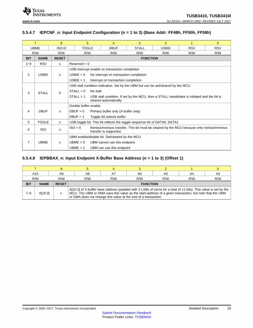
5.5.4.7 IEPCNF_n: Input Endpoint Configuration (n = 1 to 3) (Base Addr: FF48h, FF50h, FF58h)
7 6 5 4 3 2 1 0UBME ISO=0 TOGLE DBUF STALL USBIE RSV RSVR/W R/W R/W R/W R/W R/W R/W R/W
BIT NAME RESET FUNCTION1−0 RSV x Reserved = 0
2 USBIE xUSB interrupt enable on transaction completionUSBIE = 0 No interrupt on transaction completionUSBIE = 1 Interrupt on transaction completion
3 STALL 0
USB stall condition indication. Set by the UBM but can be set/cleared by the MCU.STALL = 0 No stallSTALL = 1 USB stall condition. If set by the MCU, then a STALL handshake is initiated and the bit is
cleared automatically.
4 DBUF xDouble buffer enableDBUF = 0 Primary buffer only (X-buffer only)DBUF = 1 Toggle bit selects buffer
5 TOGLE x USB toggle bit. This bit reflects the toggle sequence bit of DATA0, DATA1
6 ISO x ISO = 0 Nonisochronous transfer. This bit must be cleared by the MCU because only nonisochronoustransfer is supported.
7 UBME xUBM enable/disable bit. Set/cleared by the MCUUBME = 0 UBM cannot use this endpointUBME = 1 UBM can use this endpoint
5.5.4.8 IEPBBAX_n: Input Endpoint X-Buffer Base Address (n = 1 to 3) (Offset 1)
7 6 5 4 3 2 1 0A10 A9 A8 A7 A6 A5 A4 A3R/W R/W R/W R/W R/W R/W R/W R/W
BIT NAME RESET FUNCTION
7–0 A[10:3] xA[10:3] of X-buffer base address (padded with 3 LSBs of zeros for a total of 11 bits). This value is set by theMCU. The UBM or DMA uses this value as the start-address of a given transaction, but note that the UBMor DMA does not change this value at the end of a transaction.
34
TUSB3410, TUSB3410ISLLS519J –MARCH 2002–REVISED JULY 2017 www.ti.com
Submit Documentation FeedbackProduct Folder Links: TUSB3410
Detailed Description Copyright © 2002–2017, Texas Instruments Incorporated
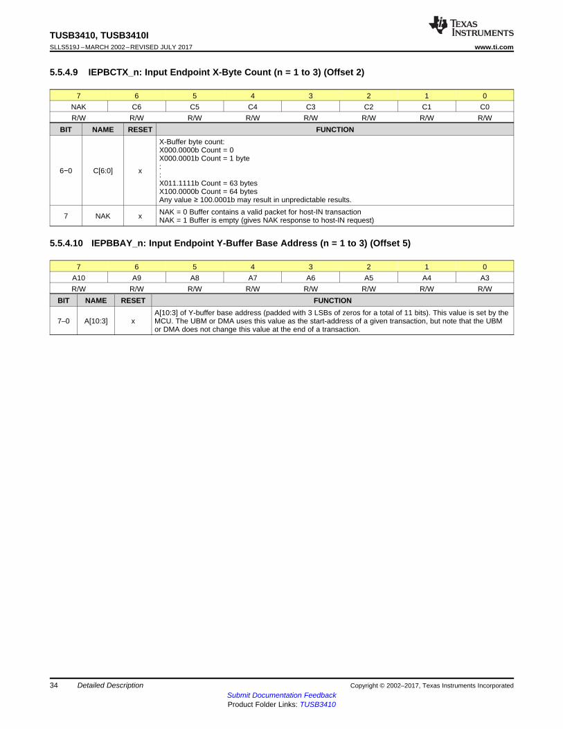
5.5.4.9 IEPBCTX_n: Input Endpoint X-Byte Count (n = 1 to 3) (Offset 2)
7 6 5 4 3 2 1 0NAK C6 C5 C4 C3 C2 C1 C0R/W R/W R/W R/W R/W R/W R/W R/W
BIT NAME RESET FUNCTION
6−0 C[6:0] x
X-Buffer byte count:X000.0000b Count = 0X000.0001b Count = 1 byte::X011.1111b Count = 63 bytesX100.0000b Count = 64 bytesAny value ≥ 100.0001b may result in unpredictable results.
7 NAK x NAK = 0 Buffer contains a valid packet for host-IN transactionNAK = 1 Buffer is empty (gives NAK response to host-IN request)
5.5.4.10 IEPBBAY_n: Input Endpoint Y-Buffer Base Address (n = 1 to 3) (Offset 5)
7 6 5 4 3 2 1 0A10 A9 A8 A7 A6 A5 A4 A3R/W R/W R/W R/W R/W R/W R/W R/W
BIT NAME RESET FUNCTION
7–0 A[10:3] xA[10:3] of Y-buffer base address (padded with 3 LSBs of zeros for a total of 11 bits). This value is set by theMCU. The UBM or DMA uses this value as the start-address of a given transaction, but note that the UBMor DMA does not change this value at the end of a transaction.
35
TUSB3410, TUSB3410Iwww.ti.com SLLS519J –MARCH 2002–REVISED JULY 2017
Submit Documentation FeedbackProduct Folder Links: TUSB3410
Detailed DescriptionCopyright © 2002–2017, Texas Instruments Incorporated
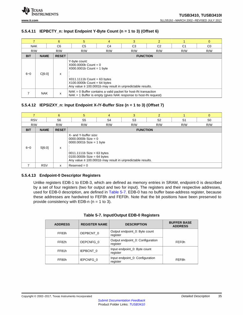
5.5.4.11 IEPBCTY_n: Input Endpoint Y-Byte Count (n = 1 to 3) (Offset 6)
7 6 5 4 3 2 1 0NAK C6 C5 C4 C3 C2 C1 C0R/W R/W R/W R/W R/W R/W R/W R/W
BIT NAME RESET FUNCTION
6−0 C[6:0] x
Y-byte count:X000.0000b Count = 0X000.0001b Count = 1 byte::X011.1111b Count = 63 bytesX100.0000b Count = 64 bytesAny value ≥ 100.0001b may result in unpredictable results.
7 NAK x NAK = 0 Buffer contains a valid packet for host-IN transactionNAK = 1 Buffer is empty (gives NAK response to host-IN request)
5.5.4.12 IEPSIZXY_n: Input Endpoint X-/Y-Buffer Size (n = 1 to 3) (Offset 7)
7 6 5 4 3 2 1 0RSV S6 S5 S4 S3 S2 S1 S0R/W R/W R/W R/W R/W R/W R/W R/W
BIT NAME RESET FUNCTION
6−0 S[6:0] x
X- and Y-buffer size:0000.0000b Size = 00000.0001b Size = 1 byte::0011.1111b Size = 63 bytes0100.0000b Size = 64 bytesAny value ≥ 100.0001b may result in unpredictable results.
7 RSV x Reserved = 0
5.5.4.13 Endpoint-0 Descriptor Registers
Unlike registers EDB-1 to EDB-3, which are defined as memory entries in SRAM, endpoint-0 is describedby a set of four registers (two for output and two for input). The registers and their respective addresses,used for EDB-0 description, are defined in Table 5-7. EDB-0 has no buffer base-address register, becausethese addresses are hardwired to FEF8h and FEF0h. Note that the bit positions have been preserved toprovide consistency with EDB-n (n = 1 to 3).
Table 5-7. Input/Output EDB-0 Registers
ADDRESS REGISTER NAME DESCRIPTION BUFFER BASEADDRESS
FF83h OEPBCNT_0 Output endpoint_0: Byte countregister
FF82h OEPCNFG_0 Output endpoint_0: Configurationregister FEF0h
FF81h IEPBCNT_0 Input endpoint_0: Byte countregister
FF80h IEPCNFG_0 Input endpoint_0: Configurationregister FEF8h

36
TUSB3410, TUSB3410ISLLS519J –MARCH 2002–REVISED JULY 2017 www.ti.com
Submit Documentation FeedbackProduct Folder Links: TUSB3410
Detailed Description Copyright © 2002–2017, Texas Instruments Incorporated
5.5.4.13.1 IEPCNFG_0: Input Endpoint-0 Configuration Register (Addr:FF80h)
7 6 5 4 3 2 1 0UBME RSV TOGLE RSV STALL USBIE RSV RSVR/W R/O R/O R/O R/W R/W R/O R/O
BIT NAME RESET FUNCTION1−0 RSV 0 Reserved = 0
2 USBIE 0USB interrupt enable on transaction completion. Set/cleared by the MCU.USBIE = 0 No interruptUSBIE = 1 Interrupt on transaction completion
3 STALL 0
USB stall condition indication. Set/cleared by the MCUSTALL = 0 No stallSTALL = 1 USB stall condition. If set by the MCU, then a STALL handshake is initiated and the bit is cleared
automatically by the next setup transaction.4 RSV 0 Reserved = 05 TOGLE 0 USB toggle bit. This bit reflects the toggle sequence bit of DATA0, DATA1.6 RSV 0 Reserved = 0
7 UBME 0UBM enable/disable bit. Set/cleared by the MCUUBME = 0 UBM cannot use this endpointUBME = 1 UBM can use this endpoint
5.5.4.13.2 IEPBCNT_0: Input Endpoint-0 Byte Count Register (Addr:FF81h)
7 6 5 4 3 2 1 0NAK RSV RSV RSV C3 C2 C1 C0R/W R/O R/O R/O R/W R/W R/W R/W
BIT NAME RESET FUNCTION
3−0 C[3:0] 0h
Byte count:0000b Count = 0::0111b Count = 71000b Count = 81001b to 1111b are reserved. (If used, they default to 8)
6−4 RSV 0 Reserved = 0
7 NAK 1 NAK = 0NAK = 1
Buffer contains a valid packet for host-IN transactionBuffer is empty (gives NAK response to host-IN request)
37
TUSB3410, TUSB3410Iwww.ti.com SLLS519J –MARCH 2002–REVISED JULY 2017
Submit Documentation FeedbackProduct Folder Links: TUSB3410
Detailed DescriptionCopyright © 2002–2017, Texas Instruments Incorporated
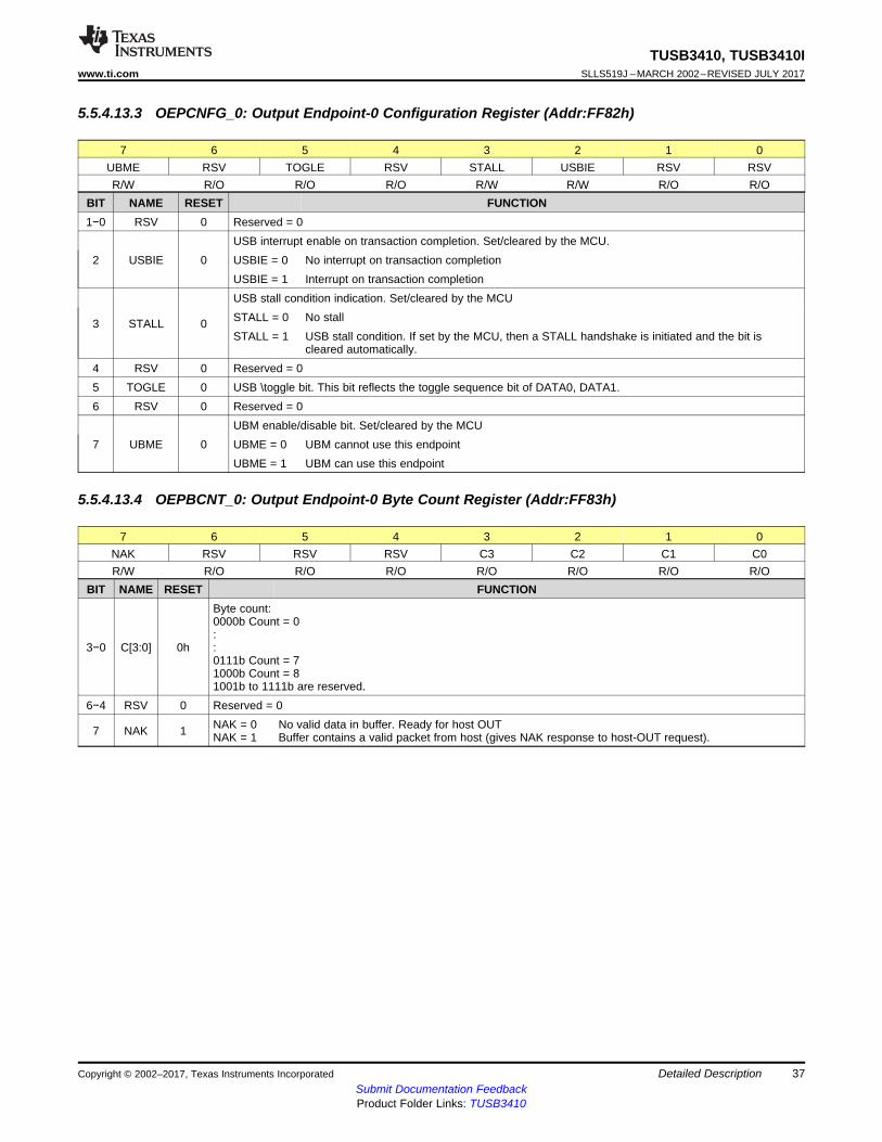
5.5.4.13.3 OEPCNFG_0: Output Endpoint-0 Configuration Register (Addr:FF82h)
7 6 5 4 3 2 1 0UBME RSV TOGLE RSV STALL USBIE RSV RSVR/W R/O R/O R/O R/W R/W R/O R/O
BIT NAME RESET FUNCTION1−0 RSV 0 Reserved = 0
2 USBIE 0USB interrupt enable on transaction completion. Set/cleared by the MCU.USBIE = 0 No interrupt on transaction completionUSBIE = 1 Interrupt on transaction completion
3 STALL 0
USB stall condition indication. Set/cleared by the MCUSTALL = 0 No stallSTALL = 1 USB stall condition. If set by the MCU, then a STALL handshake is initiated and the bit is
cleared automatically.4 RSV 0 Reserved = 05 TOGLE 0 USB \toggle bit. This bit reflects the toggle sequence bit of DATA0, DATA1.6 RSV 0 Reserved = 0
7 UBME 0UBM enable/disable bit. Set/cleared by the MCUUBME = 0 UBM cannot use this endpointUBME = 1 UBM can use this endpoint
5.5.4.13.4 OEPBCNT_0: Output Endpoint-0 Byte Count Register (Addr:FF83h)
7 6 5 4 3 2 1 0NAK RSV RSV RSV C3 C2 C1 C0R/W R/O R/O R/O R/O R/O R/O R/O
BIT NAME RESET FUNCTION
3−0 C[3:0] 0h
Byte count:0000b Count = 0::0111b Count = 71000b Count = 81001b to 1111b are reserved.
6−4 RSV 0 Reserved = 0
7 NAK 1 NAK = 0NAK = 1
No valid data in buffer. Ready for host OUTBuffer contains a valid packet from host (gives NAK response to host-OUT request).
38
TUSB3410, TUSB3410ISLLS519J –MARCH 2002–REVISED JULY 2017 www.ti.com
Submit Documentation FeedbackProduct Folder Links: TUSB3410
Detailed Description Copyright © 2002–2017, Texas Instruments Incorporated
5.5.5 USB Registers
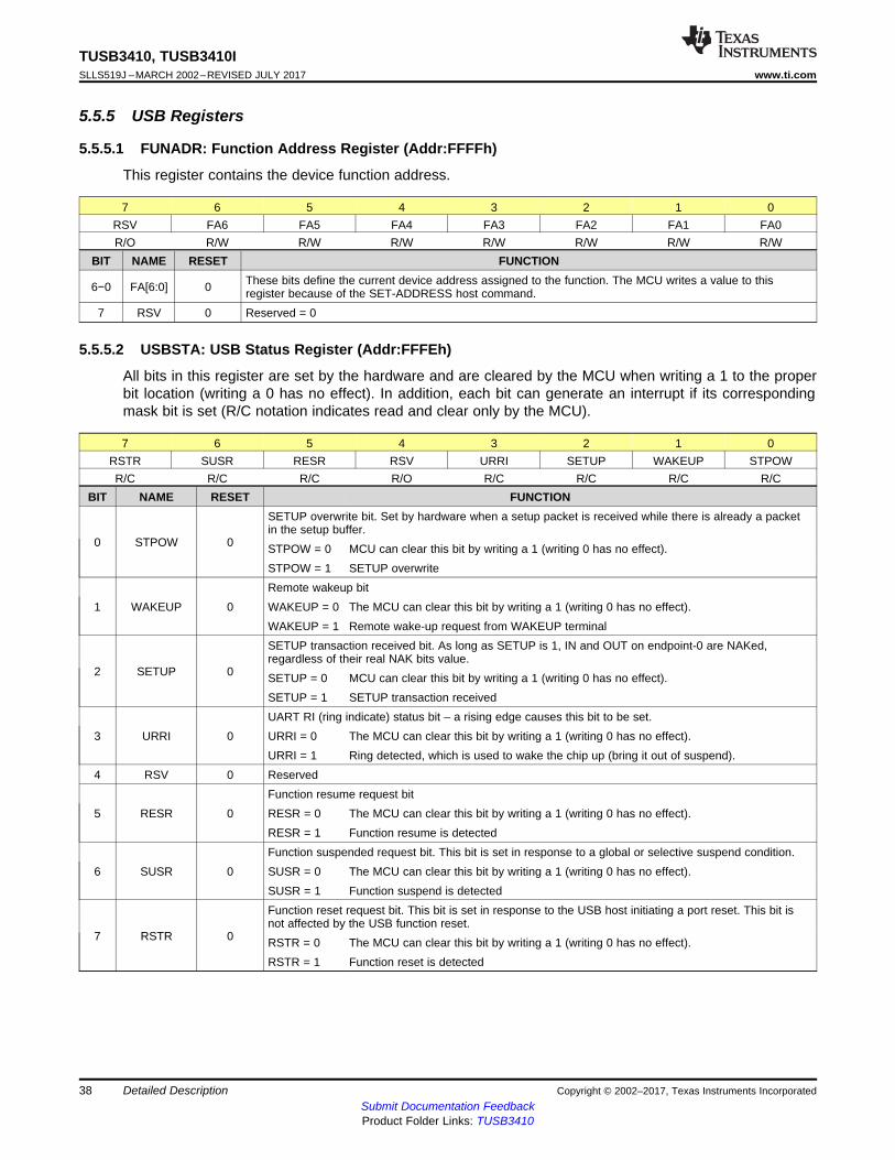
5.5.5.1 FUNADR: Function Address Register (Addr:FFFFh)
This register contains the device function address.
7 6 5 4 3 2 1 0RSV FA6 FA5 FA4 FA3 FA2 FA1 FA0R/O R/W R/W R/W R/W R/W R/W R/W
BIT NAME RESET FUNCTION
6−0 FA[6:0] 0 These bits define the current device address assigned to the function. The MCU writes a value to thisregister because of the SET-ADDRESS host command.
7 RSV 0 Reserved = 0
5.5.5.2 USBSTA: USB Status Register (Addr:FFFEh)
All bits in this register are set by the hardware and are cleared by the MCU when writing a 1 to the properbit location (writing a 0 has no effect). In addition, each bit can generate an interrupt if its correspondingmask bit is set (R/C notation indicates read and clear only by the MCU).
7 6 5 4 3 2 1 0RSTR SUSR RESR RSV URRI SETUP WAKEUP STPOWR/C R/C R/C R/O R/C R/C R/C R/C
BIT NAME RESET FUNCTION
0 STPOW 0
SETUP overwrite bit. Set by hardware when a setup packet is received while there is already a packetin the setup buffer.STPOW = 0 MCU can clear this bit by writing a 1 (writing 0 has no effect).STPOW = 1 SETUP overwrite
1 WAKEUP 0Remote wakeup bitWAKEUP = 0 The MCU can clear this bit by writing a 1 (writing 0 has no effect).WAKEUP = 1 Remote wake-up request from WAKEUP terminal
2 SETUP 0
SETUP transaction received bit. As long as SETUP is 1, IN and OUT on endpoint-0 are NAKed,regardless of their real NAK bits value.SETUP = 0 MCU can clear this bit by writing a 1 (writing 0 has no effect).SETUP = 1 SETUP transaction received
3 URRI 0UART RI (ring indicate) status bit – a rising edge causes this bit to be set.URRI = 0 The MCU can clear this bit by writing a 1 (writing 0 has no effect).URRI = 1 Ring detected, which is used to wake the chip up (bring it out of suspend).
4 RSV 0 Reserved
5 RESR 0Function resume request bitRESR = 0 The MCU can clear this bit by writing a 1 (writing 0 has no effect).RESR = 1 Function resume is detected
6 SUSR 0Function suspended request bit. This bit is set in response to a global or selective suspend condition.SUSR = 0 The MCU can clear this bit by writing a 1 (writing 0 has no effect).SUSR = 1 Function suspend is detected
7 RSTR 0
Function reset request bit. This bit is set in response to the USB host initiating a port reset. This bit isnot affected by the USB function reset.RSTR = 0 The MCU can clear this bit by writing a 1 (writing 0 has no effect).RSTR = 1 Function reset is detected
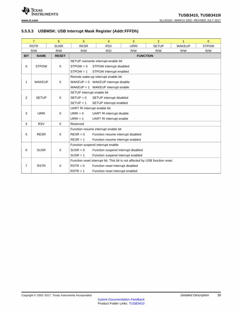
39
TUSB3410, TUSB3410Iwww.ti.com SLLS519J –MARCH 2002–REVISED JULY 2017
Submit Documentation FeedbackProduct Folder Links: TUSB3410
Detailed DescriptionCopyright © 2002–2017, Texas Instruments Incorporated
5.5.5.3 USBMSK: USB Interrupt Mask Register (Addr:FFFDh)
7 6 5 4 3 2 1 0RSTR SUSR RESR RSV URRI SETUP WAKEUP STPOWR/W R/W R/W R/O R/W R/W R/W R/W
BIT NAME RESET FUNCTION
0 STPOW 0SETUP overwrite interrupt-enable bitSTPOW = 0 STPOW interrupt disabledSTPOW = 1 STPOW interrupt enabled
1 WAKEUP 0Remote wake-up interrupt enable bitWAKEUP = 0 WAKEUP interrupt disableWAKEUP = 1 WAKEUP interrupt enable
2 SETUP 0SETUP interrupt enable bitSETUP = 0 SETUP interrupt disabledSETUP = 1 SETUP interrupt enabled
3 URRI 0UART RI interrupt enable bitURRI = 0 UART RI interrupt disableURRI = 1 UART RI interrupt enable
4 RSV 0 Reserved
5 RESR 0Function resume interrupt enable bitRESR = 0 Function resume interrupt disabledRESR = 1 Function resume interrupt enabled
6 SUSR 0Function suspend interrupt enableSUSR = 0 Function suspend interrupt disabledSUSR = 1 Function suspend interrupt enabled
7 RSTR 0Function reset interrupt bit. This bit is not affected by USB function reset.RSTR = 0 Function reset interrupt disabledRSTR = 1 Function reset interrupt enabled
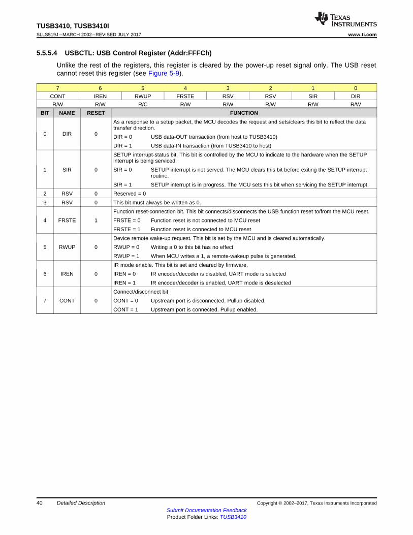
40
TUSB3410, TUSB3410ISLLS519J –MARCH 2002–REVISED JULY 2017 www.ti.com
Submit Documentation FeedbackProduct Folder Links: TUSB3410
Detailed Description Copyright © 2002–2017, Texas Instruments Incorporated
5.5.5.4 USBCTL: USB Control Register (Addr:FFFCh)
Unlike the rest of the registers, this register is cleared by the power-up reset signal only. The USB resetcannot reset this register (see Figure 5-9).
7 6 5 4 3 2 1 0CONT IREN RWUP FRSTE RSV RSV SIR DIRR/W R/W R/C R/W R/W R/W R/W R/W
BIT NAME RESET FUNCTION
0 DIR 0
As a response to a setup packet, the MCU decodes the request and sets/clears this bit to reflect the datatransfer direction.DIR = 0 USB data-OUT transaction (from host to TUSB3410)DIR = 1 USB data-IN transaction (from TUSB3410 to host)
1 SIR 0
SETUP interrupt-status bit. This bit is controlled by the MCU to indicate to the hardware when the SETUPinterrupt is being serviced.SIR = 0 SETUP interrupt is not served. The MCU clears this bit before exiting the SETUP interrupt
routine.SIR = 1 SETUP interrupt is in progress. The MCU sets this bit when servicing the SETUP interrupt.
2 RSV 0 Reserved = 03 RSV 0 This bit must always be written as 0.
4 FRSTE 1Function reset-connection bit. This bit connects/disconnects the USB function reset to/from the MCU reset.FRSTE = 0 Function reset is not connected to MCU resetFRSTE = 1 Function reset is connected to MCU reset
5 RWUP 0Device remote wake-up request. This bit is set by the MCU and is cleared automatically.RWUP = 0 Writing a 0 to this bit has no effectRWUP = 1 When MCU writes a 1, a remote-wakeup pulse is generated.
6 IREN 0IR mode enable. This bit is set and cleared by firmware.IREN = 0 IR encoder/decoder is disabled, UART mode is selectedIREN = 1 IR encoder/decoder is enabled, UART mode is deselected
7 CONT 0Connect/disconnect bitCONT = 0 Upstream port is disconnected. Pullup disabled.CONT = 1 Upstream port is connected. Pullup enabled.
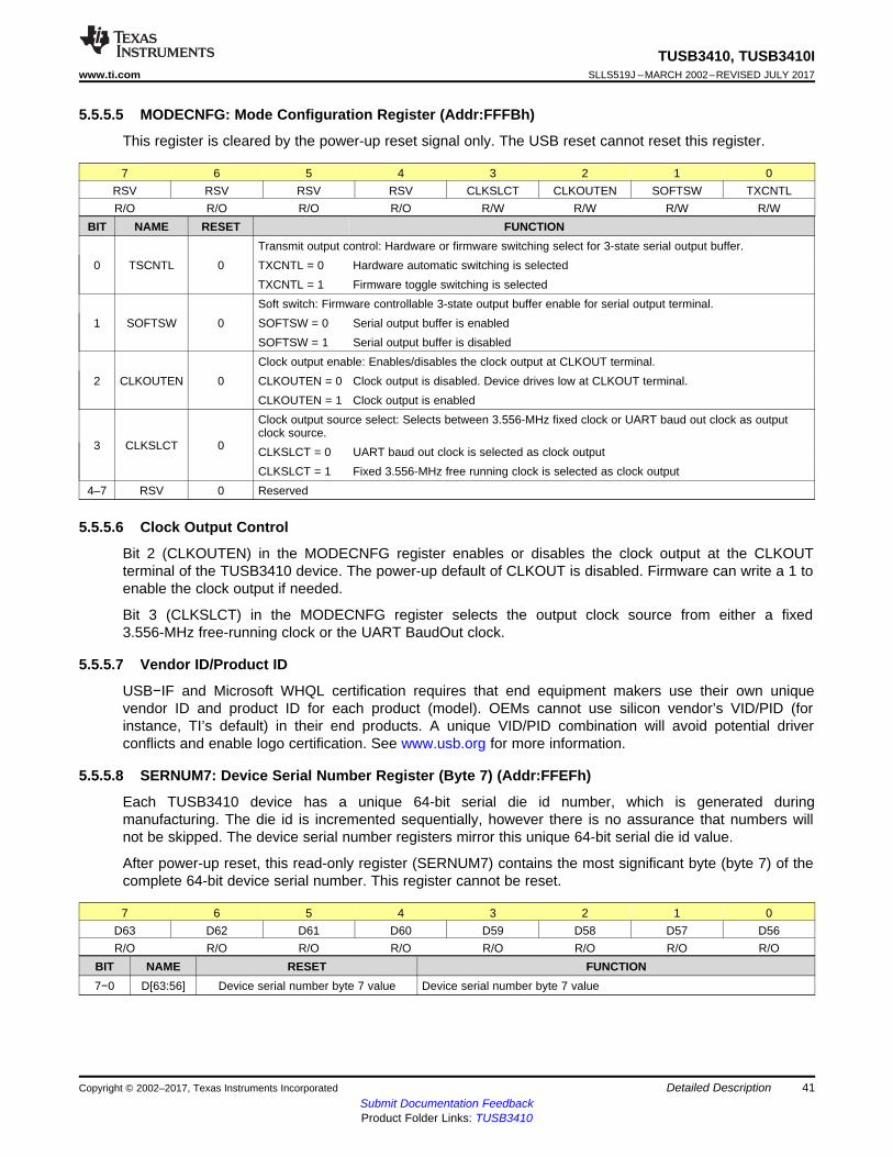
41
TUSB3410, TUSB3410Iwww.ti.com SLLS519J –MARCH 2002–REVISED JULY 2017
Submit Documentation FeedbackProduct Folder Links: TUSB3410
Detailed DescriptionCopyright © 2002–2017, Texas Instruments Incorporated
5.5.5.5 MODECNFG: Mode Configuration Register (Addr:FFFBh)
This register is cleared by the power-up reset signal only. The USB reset cannot reset this register.
7 6 5 4 3 2 1 0RSV RSV RSV RSV CLKSLCT CLKOUTEN SOFTSW TXCNTLR/O R/O R/O R/O R/W R/W R/W R/W
BIT NAME RESET FUNCTION
0 TSCNTL 0Transmit output control: Hardware or firmware switching select for 3-state serial output buffer.TXCNTL = 0 Hardware automatic switching is selectedTXCNTL = 1 Firmware toggle switching is selected
1 SOFTSW 0Soft switch: Firmware controllable 3-state output buffer enable for serial output terminal.SOFTSW = 0 Serial output buffer is enabledSOFTSW = 1 Serial output buffer is disabled
2 CLKOUTEN 0Clock output enable: Enables/disables the clock output at CLKOUT terminal.CLKOUTEN = 0 Clock output is disabled. Device drives low at CLKOUT terminal.CLKOUTEN = 1 Clock output is enabled
3 CLKSLCT 0
Clock output source select: Selects between 3.556-MHz fixed clock or UART baud out clock as outputclock source.CLKSLCT = 0 UART baud out clock is selected as clock outputCLKSLCT = 1 Fixed 3.556-MHz free running clock is selected as clock output
4–7 RSV 0 Reserved
5.5.5.6 Clock Output Control
Bit 2 (CLKOUTEN) in the MODECNFG register enables or disables the clock output at the CLKOUTterminal of the TUSB3410 device. The power-up default of CLKOUT is disabled. Firmware can write a 1 toenable the clock output if needed.
Bit 3 (CLKSLCT) in the MODECNFG register selects the output clock source from either a fixed3.556-MHz free-running clock or the UART BaudOut clock.
5.5.5.7 Vendor ID/Product ID
USB−IF and Microsoft WHQL certification requires that end equipment makers use their own uniquevendor ID and product ID for each product (model). OEMs cannot use silicon vendor’s VID/PID (forinstance, TI’s default) in their end products. A unique VID/PID combination will avoid potential driverconflicts and enable logo certification. See www.usb.org for more information.
5.5.5.8 SERNUM7: Device Serial Number Register (Byte 7) (Addr:FFEFh)
Each TUSB3410 device has a unique 64-bit serial die id number, which is generated duringmanufacturing. The die id is incremented sequentially, however there is no assurance that numbers willnot be skipped. The device serial number registers mirror this unique 64-bit serial die id value.
After power-up reset, this read-only register (SERNUM7) contains the most significant byte (byte 7) of thecomplete 64-bit device serial number. This register cannot be reset.
7 6 5 4 3 2 1 0D63 D62 D61 D60 D59 D58 D57 D56R/O R/O R/O R/O R/O R/O R/O R/O
BIT NAME RESET FUNCTION7−0 D[63:56] Device serial number byte 7 value Device serial number byte 7 value

42
TUSB3410, TUSB3410ISLLS519J –MARCH 2002–REVISED JULY 2017 www.ti.com
Submit Documentation FeedbackProduct Folder Links: TUSB3410
Detailed Description Copyright © 2002–2017, Texas Instruments Incorporated
Procedure to load device serial number value in shared RAM:• After power-up reset, the boot code copies the predefined USB descriptors to shared RAM. As a result,
the default serial number hard-coded in the boot code (0x00 hex) is copied to the shared RAM dataspace.
• The boot code checks to see if an EEPROM is present on the I2C port. If an EEPROM is present andcontains a valid device serial number as part of the USB device descriptor information stored inEEPROM, then the boot code overwrites the serial number value stored in shared RAM with the onefound in EEPROM. Otherwise, the device serial number value stored in shared RAM remainsunchanged. If firmware is stored in the EEPROM, then it is executed. This firmware can read theSERNUM7 through SERNUM0 registers and overwrite the serial number stored in RAM or store acustom number in RAM.
• In summary, the serial number value in external EEPROM has the highest priority to be loaded intoshared RAM data space. The serial number value stored in shared RAM is used as part of the validdevice descriptor information during normal operation.
5.5.5.9 SERNUM6: Device Serial Number Register (Byte 6) (Addr:FFEEh)
The device serial number registers mirror the unique 64-bit die id value.
After power-up reset, this read-only register (SERNUM6) contains byte 6 of the complete 64-bit deviceserial number. This register cannot be reset.
7 6 5 4 3 2 1 0D55 D54 D53 D52 D51 D50 D49 D48R/O R/O R/O R/O R/O R/O R/O R/O
BIT NAME RESET FUNCTION7−0 D[55:48] Device serial number byte 6 value Device serial number byte 6 value
NOTESee the procedure described in the SERNUM7 register (see Section 5.5.5.8) to load thedevice serial number into shared RAM.
5.5.5.10 SERNUM5: Device Serial Number Register (Byte 5) (Addr:FFEDh)
The device serial number registers mirror the unique 64-bit die id value.
After power-up reset, this read-only register (SERNUM5) contains byte 5 of the complete 64-bit deviceserial number. This register cannot be reset.
7 6 5 4 3 2 1 0D47 D46 D45 D44 D43 D42 D41 D40R/O R/O R/O R/O R/O R/O R/O R/O
BIT NAME RESET FUNCTION7−0 D[47:40] Device serial number byte 5 value Device serial number byte 5 value
NOTESee the procedure described in the SERNUM7 register (see Section 5.5.5.8) to load thedevice serial number into shared RAM.
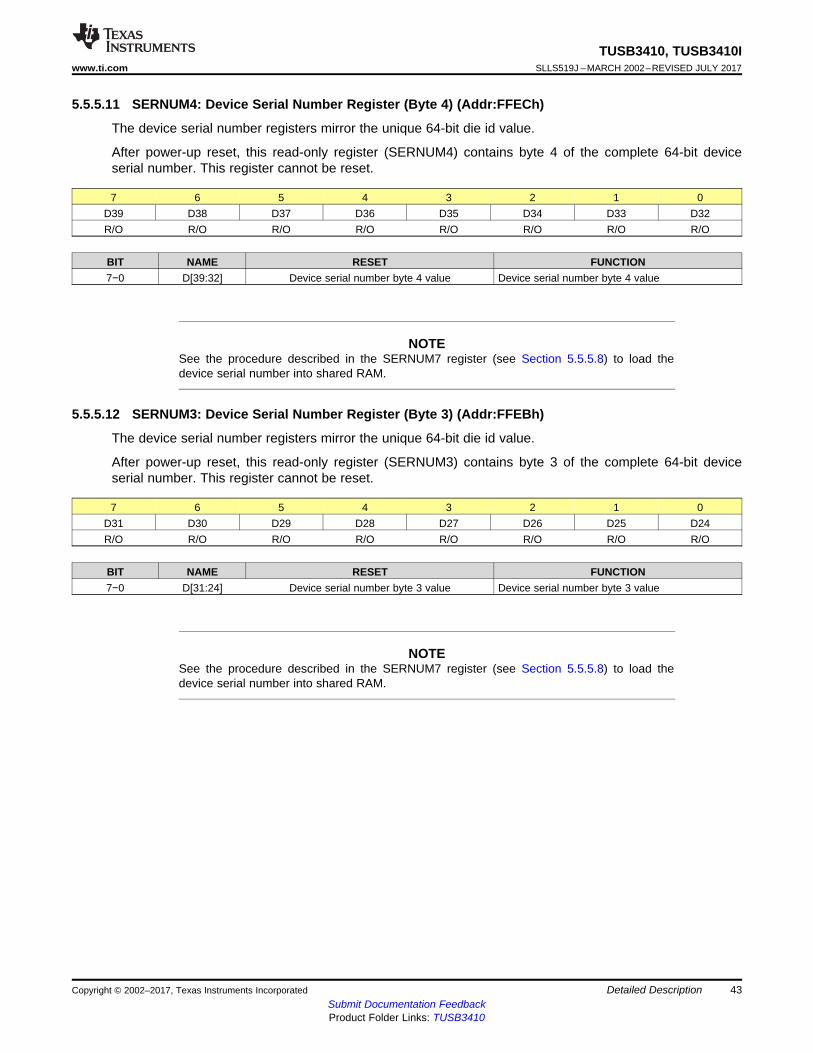
43
TUSB3410, TUSB3410Iwww.ti.com SLLS519J –MARCH 2002–REVISED JULY 2017
Submit Documentation FeedbackProduct Folder Links: TUSB3410
Detailed DescriptionCopyright © 2002–2017, Texas Instruments Incorporated
5.5.5.11 SERNUM4: Device Serial Number Register (Byte 4) (Addr:FFECh)
The device serial number registers mirror the unique 64-bit die id value.
After power-up reset, this read-only register (SERNUM4) contains byte 4 of the complete 64-bit deviceserial number. This register cannot be reset.
7 6 5 4 3 2 1 0D39 D38 D37 D36 D35 D34 D33 D32R/O R/O R/O R/O R/O R/O R/O R/O
BIT NAME RESET FUNCTION7−0 D[39:32] Device serial number byte 4 value Device serial number byte 4 value
NOTESee the procedure described in the SERNUM7 register (see Section 5.5.5.8) to load thedevice serial number into shared RAM.
5.5.5.12 SERNUM3: Device Serial Number Register (Byte 3) (Addr:FFEBh)
The device serial number registers mirror the unique 64-bit die id value.
After power-up reset, this read-only register (SERNUM3) contains byte 3 of the complete 64-bit deviceserial number. This register cannot be reset.
7 6 5 4 3 2 1 0D31 D30 D29 D28 D27 D26 D25 D24R/O R/O R/O R/O R/O R/O R/O R/O
BIT NAME RESET FUNCTION7−0 D[31:24] Device serial number byte 3 value Device serial number byte 3 value
NOTESee the procedure described in the SERNUM7 register (see Section 5.5.5.8) to load thedevice serial number into shared RAM.
44
TUSB3410, TUSB3410ISLLS519J –MARCH 2002–REVISED JULY 2017 www.ti.com
Submit Documentation FeedbackProduct Folder Links: TUSB3410
Detailed Description Copyright © 2002–2017, Texas Instruments Incorporated
5.5.5.13 SERNUM2: Device Serial Number Register (Byte 2) (Addr:FFEAh)
The device serial number registers mirror the unique 64-bit die id value.
After power-up reset, this read-only register (SERNUM2) contains byte 2 of the complete 64-bit deviceserial number. This register cannot be reset.
7 6 5 4 3 2 1 0D23 D21 D20 D19 D18 D17 D16 D15R/O R/O R/O R/O R/O R/O R/O R/O
BIT NAME RESET FUNCTION7−0 D[23:16] 0 Device serial number byte 2 value
NOTESee the procedure described in the SERNUM7 register (see Section 5.5.5.8) to load thedevice serial number into shared RAM.
5.5.5.14 SERNUM1: Device Serial Number Register (Byte 1) (Addr:FFE9h)
The device serial number registers mirror the unique 64-bit die id value.
After power-up reset, this read-only register (SERNUM1) contains byte 1 of the complete 64-bit deviceserial number. This register cannot be reset.
7 6 5 4 3 2 1 0D15 D14 D13 D12 D11 D10 D9 D8R/O R/O R/O R/O R/O R/O R/O R/O
BIT NAME RESET FUNCTION7−0 D[15:8] Device serial number byte 1 value Device serial number byte 1 value
NOTESee the procedure described in the SERNUM7 register (see Section 5.5.5.8) to load thedevice serial number into shared RAM.
45
TUSB3410, TUSB3410Iwww.ti.com SLLS519J –MARCH 2002–REVISED JULY 2017
Submit Documentation FeedbackProduct Folder Links: TUSB3410
Detailed DescriptionCopyright © 2002–2017, Texas Instruments Incorporated
5.5.5.15 SERNUM0: Device Serial Number Register (Byte 0) (Addr:FFE8h)
The device serial number registers mirror the unique 64-bit die id value.
After power-up reset, this read-only register (SERNUM0) contains byte 0 of the complete 64-bit deviceserial number. This register cannot be reset.
7 6 5 4 3 2 1 0D7 D6 D5 D4 D3 D2 D1 D0R/O R/O R/O R/O R/O R/O R/O R/O
BIT NAME RESET FUNCTION7−0 D[7:0] Device serial number byte 0 value Device serial number byte 0 value
NOTESee the procedure described in the SERNUM7 register (see Section 5.5.5.8) to load thedevice serial number into shared RAM.
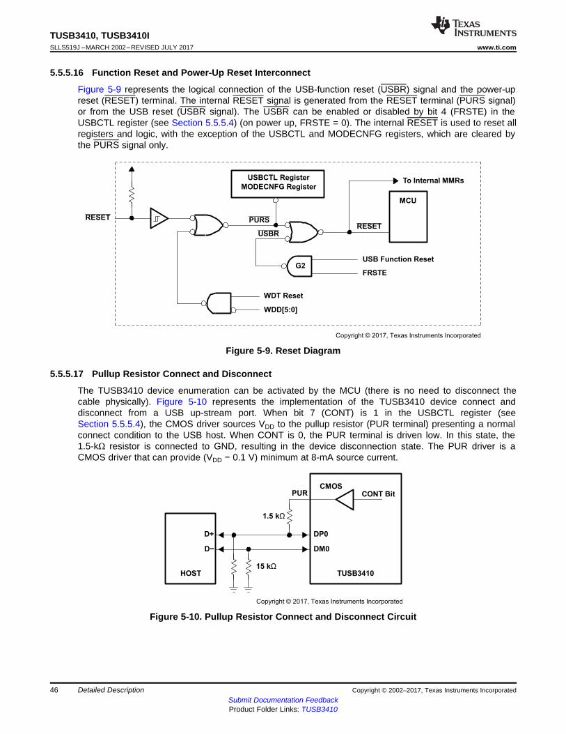
CMOSPUR CONT Bit
1.5 kΩ
D+ DP0
D− DM0
HOST
15 kΩTUSB3410
Copyright © 2017, Texas Instruments Incorporated
USBCTL Register
MODECNFG RegisterTo Internal MMRs
MCU
RESET PURS
USBRRESET
USB Function ResetG2
FRSTE
WDT Reset
WDD[5:0]
Copyright © 2017, Texas Instruments Incorporated
46
TUSB3410, TUSB3410ISLLS519J –MARCH 2002–REVISED JULY 2017 www.ti.com
Submit Documentation FeedbackProduct Folder Links: TUSB3410
Detailed Description Copyright © 2002–2017, Texas Instruments Incorporated
5.5.5.16 Function Reset and Power-Up Reset Interconnect
Figure 5-9 represents the logical connection of the USB-function reset (USBR) signal and the power-upreset (RESET) terminal. The internal RESET signal is generated from the RESET terminal (PURS signal)or from the USB reset (USBR signal). The USBR can be enabled or disabled by bit 4 (FRSTE) in theUSBCTL register (see Section 5.5.5.4) (on power up, FRSTE = 0). The internal RESET is used to reset allregisters and logic, with the exception of the USBCTL and MODECNFG registers, which are cleared bythe PURS signal only.
Figure 5-9. Reset Diagram
5.5.5.17 Pullup Resistor Connect and Disconnect
The TUSB3410 device enumeration can be activated by the MCU (there is no need to disconnect thecable physically). Figure 5-10 represents the implementation of the TUSB3410 device connect anddisconnect from a USB up-stream port. When bit 7 (CONT) is 1 in the USBCTL register (seeSection 5.5.5.4), the CMOS driver sources VDD to the pullup resistor (PUR terminal) presenting a normalconnect condition to the USB host. When CONT is 0, the PUR terminal is driven low. In this state, the1.5-kΩ resistor is connected to GND, resulting in the device disconnection state. The PUR driver is aCMOS driver that can provide (VDD − 0.1 V) minimum at 8-mA source current.
Figure 5-10. Pullup Resistor Connect and Disconnect Circuit
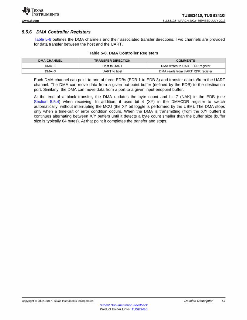
47
TUSB3410, TUSB3410Iwww.ti.com SLLS519J –MARCH 2002–REVISED JULY 2017
Submit Documentation FeedbackProduct Folder Links: TUSB3410
Detailed DescriptionCopyright © 2002–2017, Texas Instruments Incorporated
5.5.6 DMA Controller RegistersTable 5-8 outlines the DMA channels and their associated transfer directions. Two channels are providedfor data transfer between the host and the UART.
Table 5-8. DMA Controller Registers
DMA CHANNEL TRANSFER DIRECTION COMMENTSDMA−1 Host to UART DMA writes to UART TDR registerDMA−3 UART to host DMA reads from UART RDR register
Each DMA channel can point to one of three EDBs (EDB-1 to EDB-3) and transfer data to/from the UARTchannel. The DMA can move data from a given out-point buffer (defined by the EDB) to the destinationport. Similarly, the DMA can move data from a port to a given input-endpoint buffer.
At the end of a block transfer, the DMA updates the byte count and bit 7 (NAK) in the EDB (seeSection 5.5.4) when receiving. In addition, it uses bit 4 (XY) in the DMACDR register to switchautomatically, without interrupting the MCU (the XY bit toggle is performed by the UBM). The DMA stopsonly when a time-out or error condition occurs. When the DMA is transmitting (from the X/Y buffer) itcontinues alternating between X/Y buffers until it detects a byte count smaller than the buffer size (buffersize is typically 64 bytes). At that point it completes the transfer and stops.
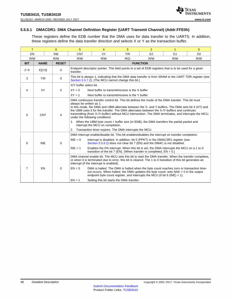
48
TUSB3410, TUSB3410ISLLS519J –MARCH 2002–REVISED JULY 2017 www.ti.com
Submit Documentation FeedbackProduct Folder Links: TUSB3410
Detailed Description Copyright © 2002–2017, Texas Instruments Incorporated
5.5.6.1 DMACDR1: DMA Channel Definition Register (UART Transmit Channel) (Addr:FFE0h)
These registers define the EDB number that the DMA uses for data transfer to the UARTS. In addition,these registers define the data transfer direction and selects X or Y as the transaction buffer.
7 6 5 4 3 2 1 0EN INE CNT XY T/R E2 E1 E0R/W R/W R/W R/W R/O R/W R/W R/W
BIT NAME RESET FUNCTION
2−0 E[2:0] 0 Endpoint descriptor pointer. This field points to a set of EDB registers that is to be used for a giventransfer.
3 T/R 0 This bit is always 1, indicating that the DMA data transfer is from SRAM to the UART TDR register (seeSection 5.5.7.2). (The MCU cannot change this bit.)
4 XY 0X/Y buffer select bit.XY = 0 Next buffer to transmit/receive is the X bufferXY = 1 Next buffer to transmit/receive is the Y buffer
5 CNT 0
DMA continuous transfer control bit. This bit defines the mode of the DMA transfer. This bit mustalways be written as 1.In this mode, the DMA and UBM alternate between the X- and Y-buffers. The DMA sets bit 4 (XY) andthe UBM uses it for the transfer. The DMA alternates between the X-/Y-buffers and continuestransmitting (from X-/Y-buffer) without MCU intervention. The DMA terminates, and interrupts the MCU,under the following conditions:1. When the UBM byte count < buffer size (in EDB), the DMA transfers the partial packet and
interrupt the MCU on completion.2. Transaction timer expires. The DMA interrupts the MCU.
6 INE 0
DMA Interrupt enable/disable bit. This bit enables/disables the interrupt on transfer completion.INE = 0 Interrupt is disabled. In addition, bit 0 (PPKT) in the DMACSR1 register (see
Section 5.5.6.2) does not clear bit 7 (EN) and the DMAC is not disabled.INE = 1 Enables the EN interrupt. When this bit is set, the DMA interrupts the MCU on a 1 to 0
transition of the bit 7 (EN). (When transfer is completed, EN = 0.)
7 EN 0
DMA channel enable bit. The MCU sets this bit to start the DMA transfer. When the transfer completes,or when it is terminated due to error, this bit is cleared. The 1 to 0 transition of this bit generates aninterrupt (if the interrupt is enabled).EN = 0 DMA is halted. The DMA is halted when the byte count reaches zero or transaction time-
out occurs. When halted, the DMA updates the byte count, sets NAK = 0 in the outputendpoint byte count register, and interrupts the MCU (if bit 6 (INE) = 1).
EN = 1 Setting this bit starts the DMA transfer.

49
TUSB3410, TUSB3410Iwww.ti.com SLLS519J –MARCH 2002–REVISED JULY 2017
Submit Documentation FeedbackProduct Folder Links: TUSB3410
Detailed DescriptionCopyright © 2002–2017, Texas Instruments Incorporated
5.5.6.2 DMACSR1: DMA Control And Status Register (UART Transmit Channel) (Addr:FFE1h)
This register defines the transaction time-out value. In addition, it contains a completion code that reportsany errors or a time-out condition.
7 6 5 4 3 2 1 00 0 0 0 0 0 0 PPKTR R R R R R R R/C
BIT NAME RESET FUNCTION
0 PPKT 0
Partial packet condition bit. This bit is set by the DMA and cleared by the MCU.PPKT =0
No partial-packet condition
PPKT =1
Partial-packet condition detected. When INE = 0, this bit does not clear bit 7 (EN) in theDMACDR1 register; therefore, the DMAC stays enabled, ready for the next transaction.Clears when MCU writes a 1. Writing a 0 has no effect.
7–1 0 These bits are read-only and return 0s when read.
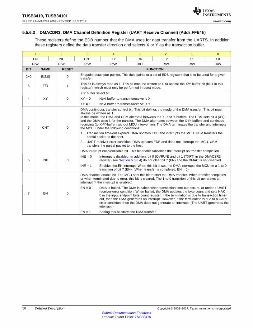
50
TUSB3410, TUSB3410ISLLS519J –MARCH 2002–REVISED JULY 2017 www.ti.com
Submit Documentation FeedbackProduct Folder Links: TUSB3410
Detailed Description Copyright © 2002–2017, Texas Instruments Incorporated
5.5.6.3 DMACDR3: DMA Channel Definition Register (UART Receive Channel) (Addr:FFE4h)
These registers define the EDB number that the DMA uses for data transfer from the UARTS. In addition,these registers define the data transfer direction and selects X or Y as the transaction buffer.
7 6 5 4 3 2 1 0EN INE CNT XY T/R E2 E1 E0R/W R/W R/W R/W R/O R/W R/W R/W
BIT NAME RESET FUNCTION
2−0 E[2:0] 0 Endpoint descriptor pointer. This field points to a set of EDB registers that is to be used for a giventransfer.
3 T/R 1 This bit is always read as 1. This bit must be written as 0 to update the X/Y buffer bit (bit 4 in thisregister), which must only be performed in burst mode.
4 XY 0X/Y buffer select bit.XY = 0 Next buffer to transmit/receive is XXY = 1 Next buffer to transmit/receive is Y
5 CNT 0
DMA continuous transfer control bit. This bit defines the mode of the DMA transfer. This bit mustalways be written as 1.In this mode, the DMA and UBM alternate between the X- and Y-buffers. The UBM sets bit 4 (XY)and the DMA uses it for the transfer. The DMA alternates between the X-/Y-buffers and continuesreceiving (to X-/Y-buffer) without MCU intervention. The DMA terminates the transfer and interruptsthe MCU, under the following conditions:1. Transaction time-out expired: DMA updates EDB and interrupts the MCU. UBM transfers the
partial packet to the host.2. UART receiver error condition: DMA updates EDB and does not interrupt the MCU. UBM
transfers the partial packet to the host.
6 INE 0
DMA Interrupt enable/disable bit. This bit enables/disables the interrupt on transfer completion.INE = 0 Interrupt is disabled. In addition, bit 0 (OVRUN) and bit 1 (TXFT) in the DMACSR3
register (see Section 5.5.6.4) do not clear bit 7 (EN) and the DMAC is not disabled.INE = 1 Enables the EN interrupt. When this bit is set, the DMA interrupts the MCU on a 1-to-0
transition of bit 7 (EN). (When transfer is completed, EN = 0).
7 EN 0
DMA channel enable bit. The MCU sets this bit to start the DMA transfer. When transfer completes,or when terminated due to error, this bit is cleared. The 1-to-0 transition of this bit generates aninterrupt (if the interrupt is enabled).EN = 0 DMA is halted. The DMA is halted when transaction time-out occurs, or under a UART
receiver-error condition. When halted, the DMA updates the byte count and sets NAK =0 in the input endpoint byte count register. If the termination is due to transaction time-out, then the DMA generates an interrupt. However, if the termination is due to a UARTerror condition, then the DMA does not generate an interrupt. (The UART generates theinterrupt.)
EN = 1 Setting this bit starts the DMA transfer.
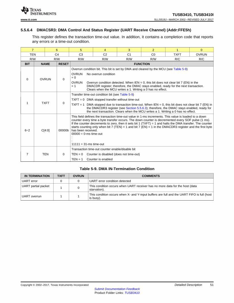
51
TUSB3410, TUSB3410Iwww.ti.com SLLS519J –MARCH 2002–REVISED JULY 2017
Submit Documentation FeedbackProduct Folder Links: TUSB3410
Detailed DescriptionCopyright © 2002–2017, Texas Instruments Incorporated
5.5.6.4 DMACSR3: DMA Control And Status Register (UART Receive Channel) (Addr:FFE5h)
This register defines the transaction time-out value. In addition, it contains a completion code that reportsany errors or a time-out condition.
7 6 5 4 3 2 1 0TEN C4 C3 C2 C1 C0 TXFT OVRUNR/W R/W R/W R/W R/W R/W R/C R/C
BIT NAME RESET FUNCTION
0 OVRUN 0
Overrun condition bit. This bit is set by DMA and cleared by the MCU (see Table 5-9)OVRUN= 0
No overrun condition
OVRUN= 1
Overrun condition detected. When IEN = 0, this bit does not clear bit 7 (EN) in theDMACDR register; therefore, the DMAC stays enabled, ready for the next transaction.Clears when the MCU writes a 1. Writing a 0 has no effect.
1 TXFT 0
Transfer time-out condition bit (see Table 5-9)TXFT = 0 DMA stopped transfer without time-outTXFT = 1 DMA stopped due to transaction time-out. When IEN = 0, this bit does not clear bit 7 (EN) in
the DMACDR3 register (see Section 5.5.6.3); therefore, the DMAC stays enabled, ready forthe next transaction. Clears when the MCU writes a 1. Writing a 0 has no effect.
6−2 C[4:0] 00000b
This field defines the transaction time-out value in 1-ms increments. This value is loaded to a downcounter every time a byte transfer occurs. The down counter is decremented every SOF pulse (1 ms).If the counter decrements to zero, then it sets bit 1 (TXFT) = 1 and halts the DMA transfer. The counterstarts counting only when bit 7 (TEN) = 1 and bit 7 (EN) = 1 in the DMACDR3 register and the first bytehas been received.00000 = 0-ms time-out::11111 = 31-ms time-out
7 TEN 0Transaction time-out counter enable/disable bitTEN = 0 Counter is disabled (does not time-out)TEN = 1 Counter is enabled
Table 5-9. DMA IN-Termination Condition
IN TERMINATION TXFT OVRUN COMMENTSUART error 0 0 UART error condition detectedUART partial packet 1 0 This condition occurs when UART receiver has no more data for the host (data
starvation).
UART overrun 1 1 This condition occurs when X- and Y-input buffers are full and the UART FIFO is full (hostis busy).
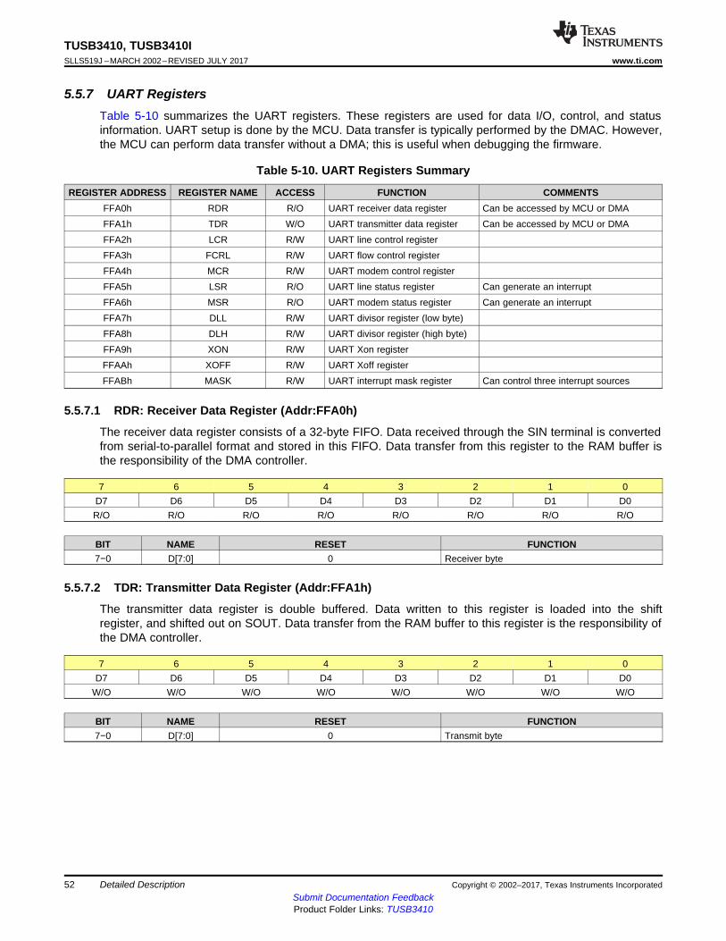
52
TUSB3410, TUSB3410ISLLS519J –MARCH 2002–REVISED JULY 2017 www.ti.com
Submit Documentation FeedbackProduct Folder Links: TUSB3410
Detailed Description Copyright © 2002–2017, Texas Instruments Incorporated
5.5.7 UART RegistersTable 5-10 summarizes the UART registers. These registers are used for data I/O, control, and statusinformation. UART setup is done by the MCU. Data transfer is typically performed by the DMAC. However,the MCU can perform data transfer without a DMA; this is useful when debugging the firmware.
Table 5-10. UART Registers Summary
REGISTER ADDRESS REGISTER NAME ACCESS FUNCTION COMMENTSFFA0h RDR R/O UART receiver data register Can be accessed by MCU or DMAFFA1h TDR W/O UART transmitter data register Can be accessed by MCU or DMAFFA2h LCR R/W UART line control registerFFA3h FCRL R/W UART flow control registerFFA4h MCR R/W UART modem control registerFFA5h LSR R/O UART line status register Can generate an interruptFFA6h MSR R/O UART modem status register Can generate an interruptFFA7h DLL R/W UART divisor register (low byte)FFA8h DLH R/W UART divisor register (high byte)FFA9h XON R/W UART Xon registerFFAAh XOFF R/W UART Xoff registerFFABh MASK R/W UART interrupt mask register Can control three interrupt sources
5.5.7.1 RDR: Receiver Data Register (Addr:FFA0h)
The receiver data register consists of a 32-byte FIFO. Data received through the SIN terminal is convertedfrom serial-to-parallel format and stored in this FIFO. Data transfer from this register to the RAM buffer isthe responsibility of the DMA controller.
7 6 5 4 3 2 1 0D7 D6 D5 D4 D3 D2 D1 D0R/O R/O R/O R/O R/O R/O R/O R/O
BIT NAME RESET FUNCTION7−0 D[7:0] 0 Receiver byte
5.5.7.2 TDR: Transmitter Data Register (Addr:FFA1h)
The transmitter data register is double buffered. Data written to this register is loaded into the shiftregister, and shifted out on SOUT. Data transfer from the RAM buffer to this register is the responsibility ofthe DMA controller.
7 6 5 4 3 2 1 0D7 D6 D5 D4 D3 D2 D1 D0
W/O W/O W/O W/O W/O W/O W/O W/O
BIT NAME RESET FUNCTION7−0 D[7:0] 0 Transmit byte
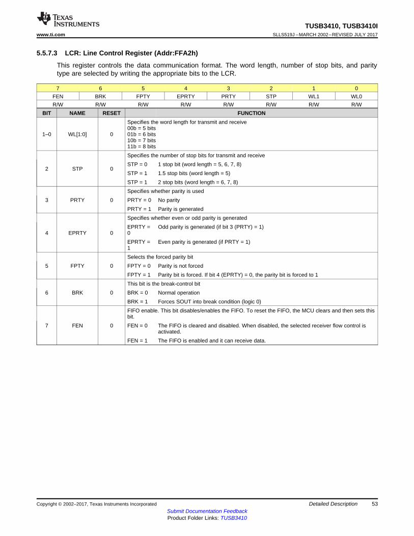
53
TUSB3410, TUSB3410Iwww.ti.com SLLS519J –MARCH 2002–REVISED JULY 2017
Submit Documentation FeedbackProduct Folder Links: TUSB3410
Detailed DescriptionCopyright © 2002–2017, Texas Instruments Incorporated
5.5.7.3 LCR: Line Control Register (Addr:FFA2h)
This register controls the data communication format. The word length, number of stop bits, and paritytype are selected by writing the appropriate bits to the LCR.
7 6 5 4 3 2 1 0FEN BRK FPTY EPRTY PRTY STP WL1 WL0R/W R/W R/W R/W R/W R/W R/W R/W
BIT NAME RESET FUNCTION
1–0 WL[1:0] 0
Specifies the word length for transmit and receive00b = 5 bits01b = 6 bits10b = 7 bits11b = 8 bits
2 STP 0
Specifies the number of stop bits for transmit and receiveSTP = 0 1 stop bit (word length = 5, 6, 7, 8)STP = 1 1.5 stop bits (word length = 5)STP = 1 2 stop bits (word length = 6, 7, 8)
3 PRTY 0Specifies whether parity is usedPRTY = 0 No parityPRTY = 1 Parity is generated
4 EPRTY 0
Specifies whether even or odd parity is generatedEPRTY =0
Odd parity is generated (if bit 3 (PRTY) = 1)
EPRTY =1
Even parity is generated (if PRTY = 1)
5 FPTY 0Selects the forced parity bitFPTY = 0 Parity is not forcedFPTY = 1 Parity bit is forced. If bit 4 (EPRTY) = 0, the parity bit is forced to 1
6 BRK 0This bit is the break-control bitBRK = 0 Normal operationBRK = 1 Forces SOUT into break condition (logic 0)
7 FEN 0
FIFO enable. This bit disables/enables the FIFO. To reset the FIFO, the MCU clears and then sets thisbit.FEN = 0 The FIFO is cleared and disabled. When disabled, the selected receiver flow control is
activated.FEN = 1 The FIFO is enabled and it can receive data.

54
TUSB3410, TUSB3410ISLLS519J –MARCH 2002–REVISED JULY 2017 www.ti.com
Submit Documentation FeedbackProduct Folder Links: TUSB3410
Detailed Description Copyright © 2002–2017, Texas Instruments Incorporated
5.5.7.4 FCRL: UART Flow Control Register (Addr:FFA3h)
This register provides the flow-control modes of operation (see Table 5-12 for more details).
7 6 5 4 3 2 1 0485E DTR RTS RXOF DSR CTS TXOA TXOFR/W R/W R/W R/W R/W R/W R/W R/W
BIT NAME RESET FUNCTION
0 TXOF 0This bit controls the transmitter Xon/Xoff flow control.TXOF = 0 Disable transmitter Xon/Xoff flow controlTXOF = 1 Enable transmitter Xon/Xoff flow control
1 TXOA 0This bit controls the transmitter Xon-on-any/Xoff flow controlTXOA = 0 Disable the transmitter Xon-on-any/Xoff flow controlTXOA = 1 Enable the transmitter Xon-on-any/Xoff flow control
2 CTS 0
Transmitter CTS flow-control enable bitCTS = 0 Disables transmitter CTS flow controlCTS = 1 CTS flow control is enabled, that is, when CTS input terminal is high, transmission
is halted; when the CTS terminal is low, transmission resumes. When loopbackmode is enabled, this bit must be set if flow control is also required.
3 DSR 0
Transmitter DSR flow-control enable bitDSR = 0 Disables transmitter DSR flow controlDSR = 1 DSR flow control is enabled, that is, when DSR input terminal is high, transmission
is halted; when the DSR terminal is low, transmission resumes. When loopbackmode is enabled, this bit must be set if flow control is also required.
4 RXOF 0This bit controls the receiver Xon/Xoff flow control.RXOF = 0 Receiver does not attempt to match Xon/Xoff charactersRXOF = 1 Receiver searches for Xon/Xoff characters
5 RTS 0
Receiver RTS flow control enable bitRTS = 0 Disables receiver RTS flow controlRTS = 1 Receiver RTS flow control is enabled. RTS output terminal goes high when the
receiver FIFO HALT trigger level is reached; it goes low, when the receiver FIFORESUME receiving trigger level is reached.
6 DTR 0
Receiver DTR flow-control enable bitDTR = 0 Disables receiver DTR flow controlDTR = 1 Receiver DTR flow control is enabled. DTR output terminal goes high when the
receiver FIFO HALT trigger level is reached; it goes low, when the receiver FIFORESUME receiving trigger level is reached.
7 485E 0
RS-485 enable bit. This bit configures the UART to control external RS-485 transceivers. Whenconfigured in half-duplex mode (485E = 1), RTS or DTR can be used to enable the RS-485 driver orreceiver (see Figure 5-5).485E = 0 UART is in normal operation mode (full duplex)485E = 1 The UART is in half duplex RS-485 mode. In this mode, RTS and DTR are active
with opposite polarity (when RTS = 0, DTR = 1). When the DMA is ready totransmit, it drives RTS = 1 (and DTR = 0) 2-bit times before the transmission starts.When the DMA terminates the transmission, it drives RTS = 0 (and DTR = 1) afterthe transmission stops. When 485E is set to 1, bit 4 (DTR) and bit 5 (RTS) in theMCR register (see Section 5.5.7.6) have no effect. Also, see bit 1 (RCVE) in theMCR register (see Section 5.5.7.6).
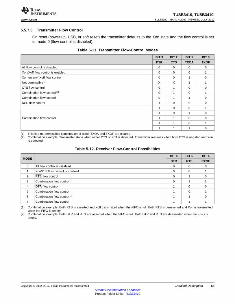
55
TUSB3410, TUSB3410Iwww.ti.com SLLS519J –MARCH 2002–REVISED JULY 2017
Submit Documentation FeedbackProduct Folder Links: TUSB3410
Detailed DescriptionCopyright © 2002–2017, Texas Instruments Incorporated
(1) This is a no permissible combination. If used, TXOA and TXOF are cleared.(2) Combination example: Transmitter stops when either CTS or Xoff is detected. Transmitter resumes when both CTS is negated and Xon
is detected.
5.5.7.5 Transmitter Flow Control
On reset (power up, USB, or soft reset) the transmitter defaults to the Xon state and the flow control is setto mode-0 (flow control is disabled).
Table 5-11. Transmitter Flow-Control Modes
BIT 3 BIT 2 BIT 1 BIT 0DSR CTS TXOA TXOF
All flow control is disabled 0 0 0 0Xon/Xoff flow control is enabled 0 0 0 1Xon on any/ Xoff flow control 0 0 1 0Not permissible (1) X X 1 1CTS flow control 0 1 0 0Combination flow control (2) 0 1 0 1Combination flow control 0 1 1 0DSR flow control 1 0 0 0
Combination flow control
1 0 0 11 0 1 01 1 0 01 1 0 11 1 1 0
(1) Combination example: Both RTS is asserted and Xoff transmitted when the FIFO is full. Both RTS is deasserted and Xon is transmittedwhen the FIFO is empty.
(2) Combination example: Both DTR and RTS are asserted when the FIFO is full. Both DTR and RTS are deasserted when the FIFO isempty.
Table 5-12. Receiver Flow-Control Possibilities
MODEBIT 6 BIT 5 BIT 4DTR RTS RXOF
0 All flow control is disabled 0 0 01 Xon/Xoff flow control is enabled 0 0 12 RTS flow control 0 1 03 Combination flow control (1) 0 1 14 DTR flow control 1 0 05 Combination flow control 1 0 16 Combination flow control (2) 1 1 07 Combination flow control 1 1 1
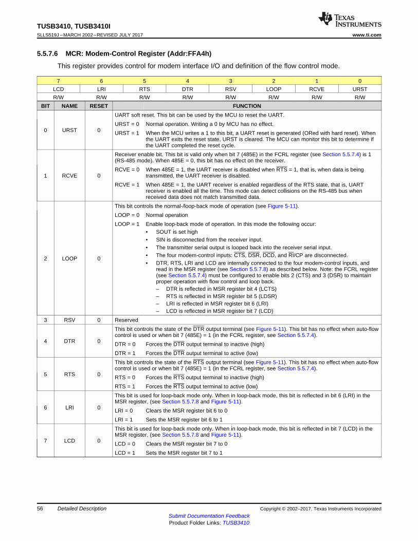
56
TUSB3410, TUSB3410ISLLS519J –MARCH 2002–REVISED JULY 2017 www.ti.com
Submit Documentation FeedbackProduct Folder Links: TUSB3410
Detailed Description Copyright © 2002–2017, Texas Instruments Incorporated
5.5.7.6 MCR: Modem-Control Register (Addr:FFA4h)
This register provides control for modem interface I/O and definition of the flow control mode.
7 6 5 4 3 2 1 0LCD LRI RTS DTR RSV LOOP RCVE URSTR/W R/W R/W R/W R/W R/W R/W R/W
BIT NAME RESET FUNCTION
0 URST 0
UART soft reset. This bit can be used by the MCU to reset the UART.URST = 0 Normal operation. Writing a 0 by MCU has no effect.URST = 1 When the MCU writes a 1 to this bit, a UART reset is generated (ORed with hard reset). When
the UART exits the reset state, URST is cleared. The MCU can monitor this bit to determine ifthe UART completed the reset cycle.
1 RCVE 0
Receiver enable bit. This bit is valid only when bit 7 (485E) in the FCRL register (see Section 5.5.7.4) is 1(RS-485 mode). When 485E = 0, this bit has no effect on the receiver.RCVE = 0 When 485E = 1, the UART receiver is disabled when RTS = 1, that is, when data is being
transmitted, the UART receiver is disabled.RCVE = 1 When 485E = 1, the UART receiver is enabled regardless of the RTS state, that is, UART
receiver is enabled all the time. This mode can detect collisions on the RS-485 bus whenreceived data does not match transmitted data.
2 LOOP 0
This bit controls the normal-/loop-back mode of operation (see Figure 5-11).LOOP = 0 Normal operationLOOP = 1 Enable loop-back mode of operation. In this mode the following occur:
• SOUT is set high• SIN is disconnected from the receiver input.• The transmitter serial output is looped back into the receiver serial input.• The four modem-control inputs: CTS, DSR, DCD, and RI/CP are disconnected.• DTR, RTS, LRI and LCD are internally connected to the four modem-control inputs, and
read in the MSR register (see Section 5.5.7.8) as described below. Note: the FCRL register(see Section 5.5.7.4) must be configured to enable bits 2 (CTS) and 3 (DSR) to maintainproper operation with flow control and loop back.– DTR is reflected in MSR register bit 4 (LCTS)– RTS is reflected in MSR register bit 5 (LDSR)– LRI is reflected in MSR register bit 6 (LRI)– LCD is reflected in MSR register bit 7 (LCD)
3 RSV 0 Reserved
4 DTR 0
This bit controls the state of the DTR output terminal (see Figure 5-11). This bit has no effect when auto-flowcontrol is used or when bit 7 (485E) = 1 (in the FCRL register, see Section 5.5.7.4).DTR = 0 Forces the DTR output terminal to inactive (high)DTR = 1 Forces the DTR output terminal to active (low)
5 RTS 0
This bit controls the state of the RTS output terminal (see Figure 5-11). This bit has no effect when auto-flowcontrol is used or when bit 7 (485E) = 1 (in the FCRL register, see Section 5.5.7.4).RTS = 0 Forces the RTS output terminal to inactive (high)RTS = 1 Forces the RTS output terminal to active (low)
6 LRI 0
This bit is used for loop-back mode only. When in loop-back mode, this bit is reflected in bit 6 (LRI) in theMSR register, (see Section 5.5.7.8 and Figure 5-11).LRI = 0 Clears the MSR register bit 6 to 0LRI = 1 Sets the MSR register bit 6 to 1
7 LCD 0
This bit is used for loop-back mode only. When in loop-back mode, this bit is reflected in bit 7 (LCD) in theMSR register, (see Section 5.5.7.8 and Figure 5-11).LCD = 0 Clears the MSR register bit 7 to 0LCD = 1 Sets the MSR register bit 7 to 1
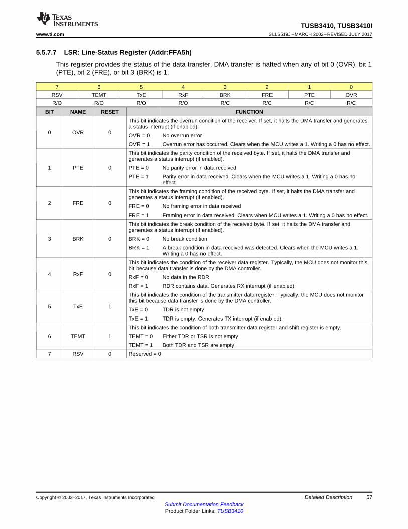
57
TUSB3410, TUSB3410Iwww.ti.com SLLS519J –MARCH 2002–REVISED JULY 2017
Submit Documentation FeedbackProduct Folder Links: TUSB3410
Detailed DescriptionCopyright © 2002–2017, Texas Instruments Incorporated
5.5.7.7 LSR: Line-Status Register (Addr:FFA5h)
This register provides the status of the data transfer. DMA transfer is halted when any of bit 0 (OVR), bit 1(PTE), bit 2 (FRE), or bit 3 (BRK) is 1.
7 6 5 4 3 2 1 0RSV TEMT TxE RxF BRK FRE PTE OVRR/O R/O R/O R/O R/C R/C R/C R/C
BIT NAME RESET FUNCTION
0 OVR 0
This bit indicates the overrun condition of the receiver. If set, it halts the DMA transfer and generatesa status interrupt (if enabled).OVR = 0 No overrun errorOVR = 1 Overrun error has occurred. Clears when the MCU writes a 1. Writing a 0 has no effect.
1 PTE 0
This bit indicates the parity condition of the received byte. If set, it halts the DMA transfer andgenerates a status interrupt (if enabled).PTE = 0 No parity error in data receivedPTE = 1 Parity error in data received. Clears when the MCU writes a 1. Writing a 0 has no
effect.
2 FRE 0
This bit indicates the framing condition of the received byte. If set, it halts the DMA transfer andgenerates a status interrupt (if enabled).FRE = 0 No framing error in data receivedFRE = 1 Framing error in data received. Clears when MCU writes a 1. Writing a 0 has no effect.
3 BRK 0
This bit indicates the break condition of the received byte. If set, it halts the DMA transfer andgenerates a status interrupt (if enabled).BRK = 0 No break conditionBRK = 1 A break condition in data received was detected. Clears when the MCU writes a 1.
Writing a 0 has no effect.
4 RxF 0
This bit indicates the condition of the receiver data register. Typically, the MCU does not monitor thisbit because data transfer is done by the DMA controller.RxF = 0 No data in the RDRRxF = 1 RDR contains data. Generates RX interrupt (if enabled).
5 TxE 1
This bit indicates the condition of the transmitter data register. Typically, the MCU does not monitorthis bit because data transfer is done by the DMA controller.TxE = 0 TDR is not emptyTxE = 1 TDR is empty. Generates TX interrupt (if enabled).
6 TEMT 1This bit indicates the condition of both transmitter data register and shift register is empty.TEMT = 0 Either TDR or TSR is not emptyTEMT = 1 Both TDR and TSR are empty
7 RSV 0 Reserved = 0

Device Terminals
CTS
DSR
Modem
Status
Register
Bit 4 LCTS
Bit 5 LDSR
Bit 6 LRI
Bit 7 LCD
RI/CP
DCD
FCRL Register Setting
Modem
Control
Register
Bit 4 DTR
Bit 5 RTS
Bit 6 LRI
Bit 7 LCD
Bit 2 LOOP FCRL Register Setting
DTR
RTS
Copyright © 2017, Texas Instruments Incorporated
58
TUSB3410, TUSB3410ISLLS519J –MARCH 2002–REVISED JULY 2017 www.ti.com
Submit Documentation FeedbackProduct Folder Links: TUSB3410
Detailed Description Copyright © 2002–2017, Texas Instruments Incorporated
Figure 5-11. MSR and MCR Registers in Loop-Back Mode
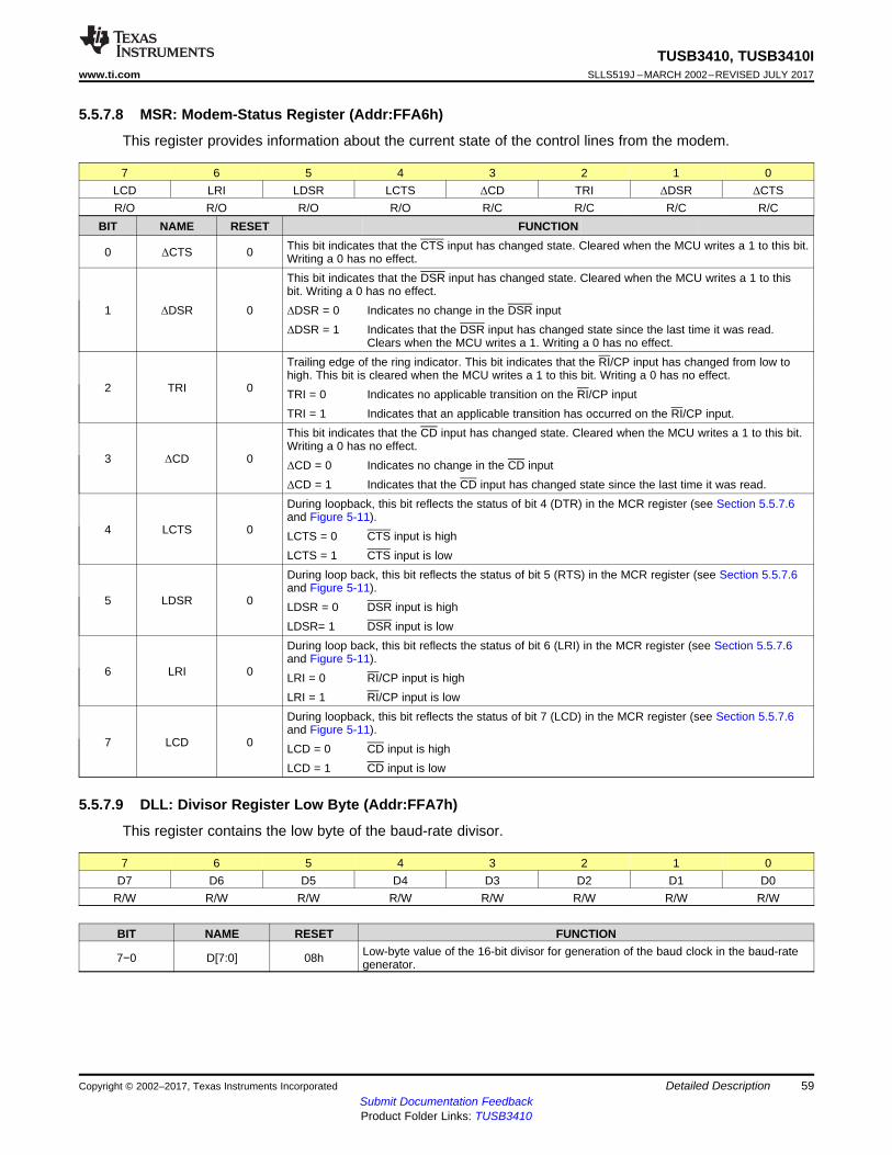
59
TUSB3410, TUSB3410Iwww.ti.com SLLS519J –MARCH 2002–REVISED JULY 2017
Submit Documentation FeedbackProduct Folder Links: TUSB3410
Detailed DescriptionCopyright © 2002–2017, Texas Instruments Incorporated
5.5.7.8 MSR: Modem-Status Register (Addr:FFA6h)
This register provides information about the current state of the control lines from the modem.
7 6 5 4 3 2 1 0LCD LRI LDSR LCTS ΔCD TRI ΔDSR ΔCTSR/O R/O R/O R/O R/C R/C R/C R/C
BIT NAME RESET FUNCTION
0 ΔCTS 0 This bit indicates that the CTS input has changed state. Cleared when the MCU writes a 1 to this bit.Writing a 0 has no effect.
1 ΔDSR 0
This bit indicates that the DSR input has changed state. Cleared when the MCU writes a 1 to thisbit. Writing a 0 has no effect.ΔDSR = 0 Indicates no change in the DSR inputΔDSR = 1 Indicates that the DSR input has changed state since the last time it was read.
Clears when the MCU writes a 1. Writing a 0 has no effect.
2 TRI 0
Trailing edge of the ring indicator. This bit indicates that the RI/CP input has changed from low tohigh. This bit is cleared when the MCU writes a 1 to this bit. Writing a 0 has no effect.TRI = 0 Indicates no applicable transition on the RI/CP inputTRI = 1 Indicates that an applicable transition has occurred on the RI/CP input.
3 ΔCD 0
This bit indicates that the CD input has changed state. Cleared when the MCU writes a 1 to this bit.Writing a 0 has no effect.ΔCD = 0 Indicates no change in the CD inputΔCD = 1 Indicates that the CD input has changed state since the last time it was read.
4 LCTS 0
During loopback, this bit reflects the status of bit 4 (DTR) in the MCR register (see Section 5.5.7.6and Figure 5-11).LCTS = 0 CTS input is highLCTS = 1 CTS input is low
5 LDSR 0
During loop back, this bit reflects the status of bit 5 (RTS) in the MCR register (see Section 5.5.7.6and Figure 5-11).LDSR = 0 DSR input is highLDSR= 1 DSR input is low
6 LRI 0
During loop back, this bit reflects the status of bit 6 (LRI) in the MCR register (see Section 5.5.7.6and Figure 5-11).LRI = 0 RI/CP input is highLRI = 1 RI/CP input is low
7 LCD 0
During loopback, this bit reflects the status of bit 7 (LCD) in the MCR register (see Section 5.5.7.6and Figure 5-11).LCD = 0 CD input is highLCD = 1 CD input is low
5.5.7.9 DLL: Divisor Register Low Byte (Addr:FFA7h)
This register contains the low byte of the baud-rate divisor.
7 6 5 4 3 2 1 0D7 D6 D5 D4 D3 D2 D1 D0
R/W R/W R/W R/W R/W R/W R/W R/W
BIT NAME RESET FUNCTION
7−0 D[7:0] 08h Low-byte value of the 16-bit divisor for generation of the baud clock in the baud-rategenerator.
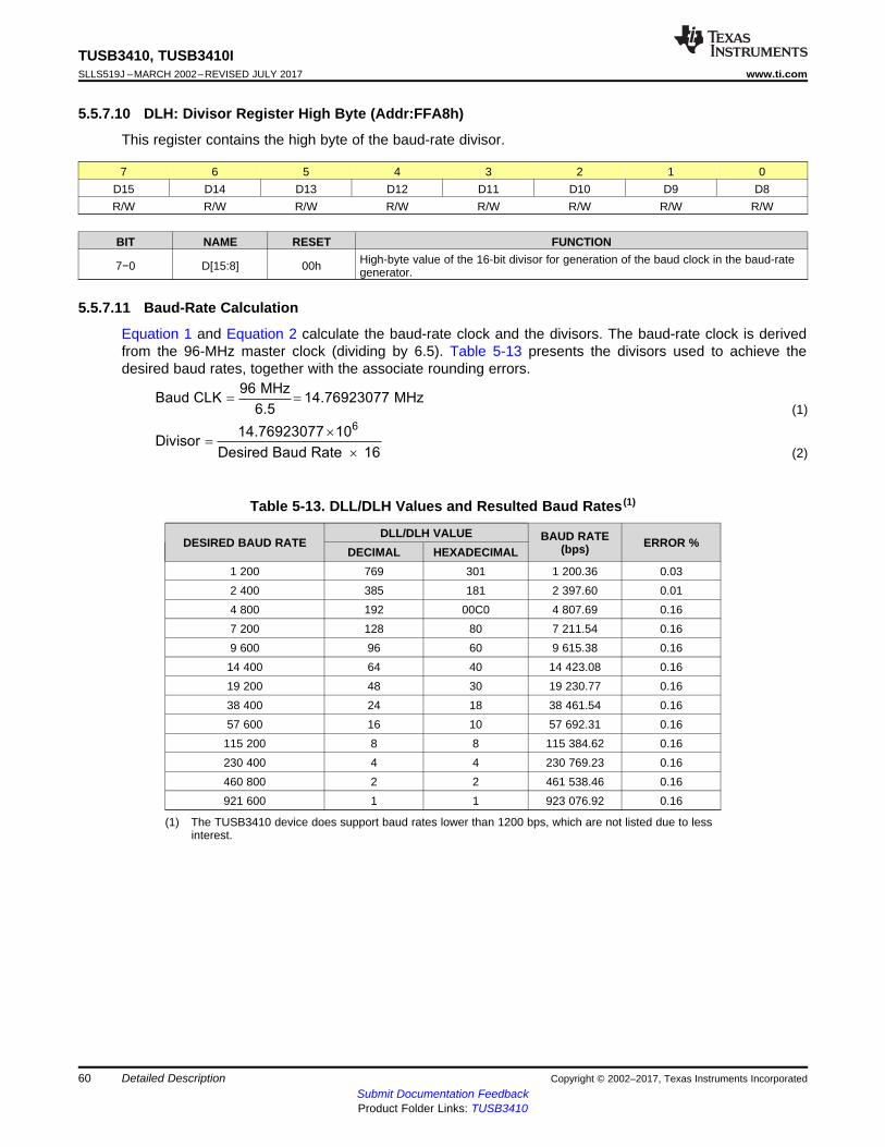
614.76923077 10
DivisorDesired Baud Rate 16
´
=
´
96 MHzBaud CLK 14.76923077 MHz
6.5= =
60
TUSB3410, TUSB3410ISLLS519J –MARCH 2002–REVISED JULY 2017 www.ti.com
Submit Documentation FeedbackProduct Folder Links: TUSB3410
Detailed Description Copyright © 2002–2017, Texas Instruments Incorporated
5.5.7.10 DLH: Divisor Register High Byte (Addr:FFA8h)
This register contains the high byte of the baud-rate divisor.
7 6 5 4 3 2 1 0D15 D14 D13 D12 D11 D10 D9 D8R/W R/W R/W R/W R/W R/W R/W R/W
BIT NAME RESET FUNCTION
7−0 D[15:8] 00h High-byte value of the 16-bit divisor for generation of the baud clock in the baud-rategenerator.
5.5.7.11 Baud-Rate Calculation
Equation 1 and Equation 2 calculate the baud-rate clock and the divisors. The baud-rate clock is derivedfrom the 96-MHz master clock (dividing by 6.5). Table 5-13 presents the divisors used to achieve thedesired baud rates, together with the associate rounding errors.
(1)
(2)
(1) The TUSB3410 device does support baud rates lower than 1200 bps, which are not listed due to lessinterest.
Table 5-13. DLL/DLH Values and Resulted Baud Rates (1)
DESIRED BAUD RATEDLL/DLH VALUE BAUD RATE
(bps) ERROR %DECIMAL HEXADECIMAL
1 200 769 301 1 200.36 0.032 400 385 181 2 397.60 0.014 800 192 00C0 4 807.69 0.167 200 128 80 7 211.54 0.169 600 96 60 9 615.38 0.1614 400 64 40 14 423.08 0.1619 200 48 30 19 230.77 0.1638 400 24 18 38 461.54 0.1657 600 16 10 57 692.31 0.16
115 200 8 8 115 384.62 0.16230 400 4 4 230 769.23 0.16460 800 2 2 461 538.46 0.16921 600 1 1 923 076.92 0.16
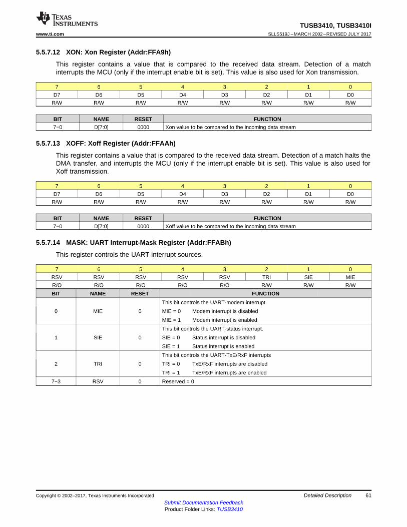
61
TUSB3410, TUSB3410Iwww.ti.com SLLS519J –MARCH 2002–REVISED JULY 2017
Submit Documentation FeedbackProduct Folder Links: TUSB3410
Detailed DescriptionCopyright © 2002–2017, Texas Instruments Incorporated
5.5.7.12 XON: Xon Register (Addr:FFA9h)
This register contains a value that is compared to the received data stream. Detection of a matchinterrupts the MCU (only if the interrupt enable bit is set). This value is also used for Xon transmission.
7 6 5 4 3 2 1 0D7 D6 D5 D4 D3 D2 D1 D0
R/W R/W R/W R/W R/W R/W R/W R/W
BIT NAME RESET FUNCTION7−0 D[7:0] 0000 Xon value to be compared to the incoming data stream
5.5.7.13 XOFF: Xoff Register (Addr:FFAAh)
This register contains a value that is compared to the received data stream. Detection of a match halts theDMA transfer, and interrupts the MCU (only if the interrupt enable bit is set). This value is also used forXoff transmission.
7 6 5 4 3 2 1 0D7 D6 D5 D4 D3 D2 D1 D0
R/W R/W R/W R/W R/W R/W R/W R/W
BIT NAME RESET FUNCTION7−0 D[7:0] 0000 Xoff value to be compared to the incoming data stream
5.5.7.14 MASK: UART Interrupt-Mask Register (Addr:FFABh)
This register controls the UART interrupt sources.
7 6 5 4 3 2 1 0RSV RSV RSV RSV RSV TRI SIE MIER/O R/O R/O R/O R/O R/W R/W R/WBIT NAME RESET FUNCTION
0 MIE 0This bit controls the UART-modem interrupt.MIE = 0 Modem interrupt is disabledMIE = 1 Modem interrupt is enabled
1 SIE 0This bit controls the UART-status interrupt.SIE = 0 Status interrupt is disabledSIE = 1 Status interrupt is enabled
2 TRI 0This bit controls the UART-TxE/RxF interruptsTRI = 0 TxE/RxF interrupts are disabledTRI = 1 TxE/RxF interrupts are enabled
7−3 RSV 0 Reserved = 0

62
TUSB3410, TUSB3410ISLLS519J –MARCH 2002–REVISED JULY 2017 www.ti.com
Submit Documentation FeedbackProduct Folder Links: TUSB3410
Detailed Description Copyright © 2002–2017, Texas Instruments Incorporated
5.5.8 Expanded GPIO Port
5.5.8.1 Input/Output and Control Registers
The TUSB3410 device has four general-purpose I/O terminals (P3.0, P3.1, P3.3, and P3.4) that arecontrolled by firmware running on the MCU. Each terminal can be controlled individually and each isimplemented with a 12-mA push/pull CMOS output with 3-state control plus input. The MCU treats theoutputs as open drain types in that the output can be driven low continuously, but a high output is drivenfor two clock cycles and then the output is high impedance.
An input terminal can be read using the MOV instruction. For example, MOV C, P3.3 reads the input onP3.3. As a precaution, be certain the associated output is high impedance before reading the input.
An output can be set high (and then high impedance) using the SETB instruction. For example, SETBP3.1 sets P3.1 high. An output can be set low using the CLR instruction, as in CLR P3.4, which sets P3.4low (driven continuously until changed).
Each GPIO terminal has an associated internal pullup resistor. It is strongly recommended that the pullupresistor remain connected to the terminal to prevent oscillations in the input buffer. The only exception is ifan external source always drives the input.
5.5.8.1.1 PUR_3: GPIO Pullup Register for Port 3 (Addr:FF9Eh)
7 6 5 4 3 2 1 0RSV RSV RSV Pin4 Pin3 RSV Pin1 Pin0R/O R/O R/O R/W R/W R/O R/W R/WBIT NAME RESET FUNCTION0 Pin0 0
The MCU may write to this register. If the MCU sets any of these bits to 1, then thepullup resistor is disconnected from the associated terminal. If the MCU clears any ofthese bits to 0, then the pullup resistor is connected from the terminal. The pullupresistor is connected to the VCC power supply.
1 Pin1 03 Pin3 04 Pin4 0
2, 5, 6, 7 RSV Reserved This bit controls the UART-status interrupt.
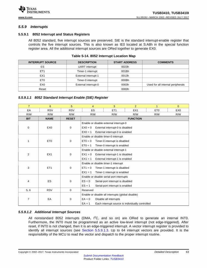
63
TUSB3410, TUSB3410Iwww.ti.com SLLS519J –MARCH 2002–REVISED JULY 2017
Submit Documentation FeedbackProduct Folder Links: TUSB3410
Detailed DescriptionCopyright © 2002–2017, Texas Instruments Incorporated
5.5.9 Interrupts
5.5.9.1 8052 Interrupt and Status Registers
All 8052 standard, five interrupt sources are preserved. SIE is the standard interrupt-enable register thatcontrols the five interrupt sources. This is also known as IE0 located at S:A8h in the special functionregister area. All the additional interrupt sources are ORed together to generate EX0.
Table 5-14. 8052 Interrupt Location Map
INTERRUPT SOURCE DESCRIPTION START ADDRESS COMMENTSES UART interrupt 0023hET1 Timer-1 interrupt 001BhEX1 External interrupt-1 0013hET0 Timer-0 interrupt 000BhEX0 External interrupt-0 0003h Used for all internal peripherals
Reset 0000h
5.5.9.1.1 8052 Standard Interrupt Enable (SIE) Register
7 6 5 4 3 2 1 0EA RSV RSV ES ET1 EX1 ET0 EX0
R/W R/W R/W R/W R/W R/W R/W R/WBIT NAME RESET FUNCTION
0 EX0 0Enable or disable external interrupt-0EX0 = 0 External interrupt-0 is disabledEX0 = 1 External interrupt-0 is enabled
1 ET0 0Enable or disable timer-0 interruptET0 = 0 Timer-0 interrupt is disabledET0 = 1 Timer-0 interrupt is enabled
2 EX1 0Enable or disable external interrupt-1EX1 = 0 External interrupt-1 is disabledEX1 = 1 External interrupt-1 is enabled
3 ET1 0Enable or disable timer-1 interruptET1 = 0 Timer-1 interrupt is disabledEX1 = 1 Timer-1 interrupt is enabled
4 ES 0Enable or disable serial port interruptsES = 0 Serial-port interrupt is disabledES = 1 Serial-port interrupt is enabled
5, 6 RSV 0 Reserved
7 EA 0Enable or disable all interrupts (global disable)EA = 0 Disable all interruptsEA = 1 Each interrupt source is individually controlled
5.5.9.1.2 Additional Interrupt Sources
All nonstandard 8052 interrupts (DMA, I2C, and so on) are ORed to generate an internal INT0.Furthermore, the INT0 must be programmed as an active low-level interrupt (not edge-triggered). Afterreset, if INT0 is not changed, then it is an edge-triggered interrupt. A vector interrupt register is provided toidentify all interrupt sources (see Section 5.5.9.1.3. Up to 64 interrupt vectors are provided. It is theresponsibility of the MCU to read the vector and dispatch to the proper interrupt routine.
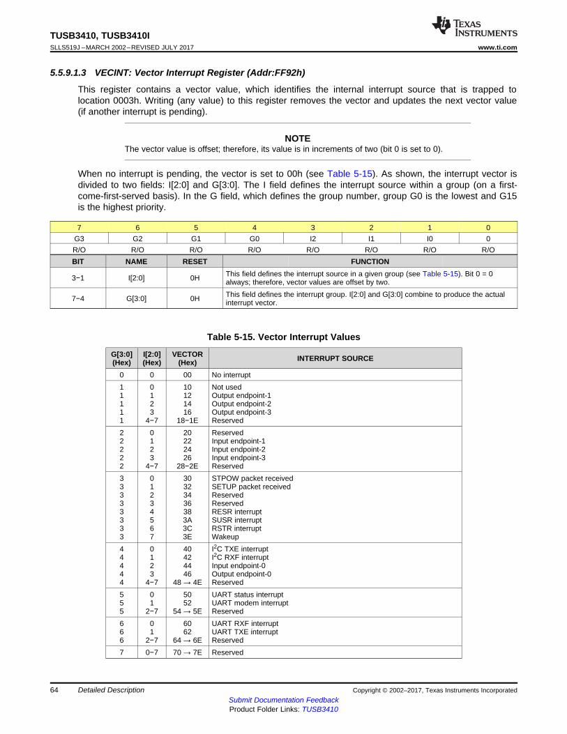
64
TUSB3410, TUSB3410ISLLS519J –MARCH 2002–REVISED JULY 2017 www.ti.com
Submit Documentation FeedbackProduct Folder Links: TUSB3410
Detailed Description Copyright © 2002–2017, Texas Instruments Incorporated
5.5.9.1.3 VECINT: Vector Interrupt Register (Addr:FF92h)
This register contains a vector value, which identifies the internal interrupt source that is trapped tolocation 0003h. Writing (any value) to this register removes the vector and updates the next vector value(if another interrupt is pending).
NOTEThe vector value is offset; therefore, its value is in increments of two (bit 0 is set to 0).
When no interrupt is pending, the vector is set to 00h (see Table 5-15). As shown, the interrupt vector isdivided to two fields: I[2:0] and G[3:0]. The I field defines the interrupt source within a group (on a first-come-first-served basis). In the G field, which defines the group number, group G0 is the lowest and G15is the highest priority.
7 6 5 4 3 2 1 0G3 G2 G1 G0 I2 I1 I0 0R/O R/O R/O R/O R/O R/O R/O R/OBIT NAME RESET FUNCTION
3−1 I[2:0] 0H This field defines the interrupt source in a given group (see Table 5-15). Bit 0 = 0always; therefore, vector values are offset by two.
7−4 G[3:0] 0H This field defines the interrupt group. I[2:0] and G[3:0] combine to produce the actualinterrupt vector.
Table 5-15. Vector Interrupt Values
G[3:0](Hex)
I[2:0](Hex)
VECTOR(Hex) INTERRUPT SOURCE
0 0 00 No interrupt11111
0123
4−7
10121416
18−1E
Not usedOutput endpoint-1Output endpoint-2Output endpoint-3Reserved
22222
0123
4−7
20222426
28−2E
ReservedInput endpoint-1Input endpoint-2Input endpoint-3Reserved
33333333
01234567
30323436383A3C3E
STPOW packet receivedSETUP packet receivedReservedReservedRESR interruptSUSR interruptRSTR interruptWakeup
44444
0123
4−7
40424446
48 → 4E
I2C TXE interruptI2C RXF interruptInput endpoint-0Output endpoint-0Reserved
555
01
2−7
5052
54 → 5E
UART status interruptUART modem interruptReserved
666
01
2−7
6062
64 → 6E
UART RXF interruptUART TXE interruptReserved
7 0−7 70 → 7E Reserved
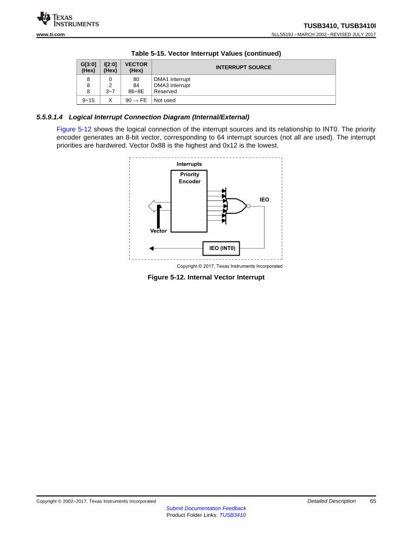
Interrupts
Priority
Encoder
IEO
Vector
IEO (INT0)
Copyright © 2017, Texas Instruments Incorporated
65
TUSB3410, TUSB3410Iwww.ti.com SLLS519J –MARCH 2002–REVISED JULY 2017
Submit Documentation FeedbackProduct Folder Links: TUSB3410
Detailed DescriptionCopyright © 2002–2017, Texas Instruments Incorporated
Table 5-15. Vector Interrupt Values (continued)G[3:0](Hex)
I[2:0](Hex)
VECTOR(Hex) INTERRUPT SOURCE
888
02
3−7
8084
86−8E
DMA1 interruptDMA3 interruptReserved
9−15 X 90 → FE Not used
5.5.9.1.4 Logical Interrupt Connection Diagram (Internal/External)
Figure 5-12 shows the logical connection of the interrupt sources and its relationship to INT0. The priorityencoder generates an 8-bit vector, corresponding to 64 interrupt sources (not all are used). The interruptpriorities are hardwired. Vector 0x88 is the highest and 0x12 is the lowest.
Figure 5-12. Internal Vector Interrupt
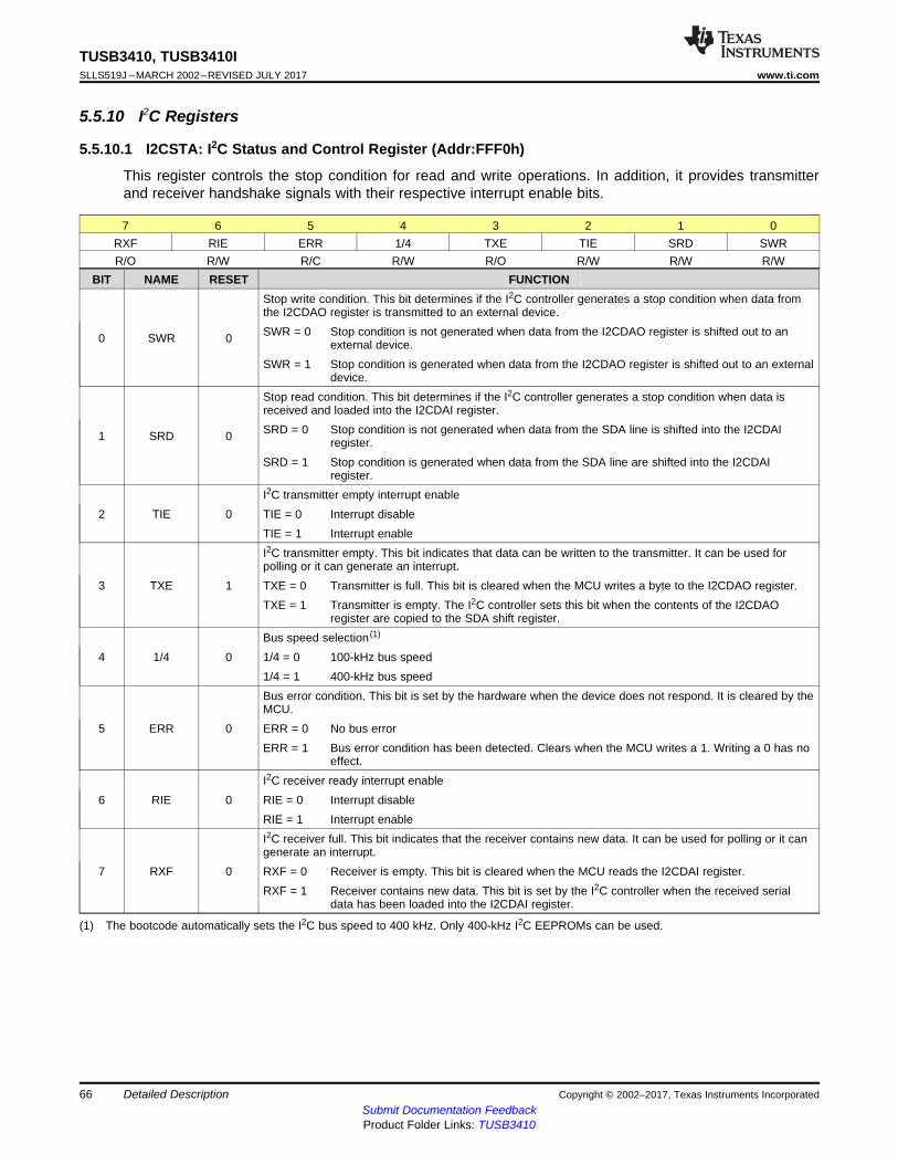
66
TUSB3410, TUSB3410ISLLS519J –MARCH 2002–REVISED JULY 2017 www.ti.com
Submit Documentation FeedbackProduct Folder Links: TUSB3410
Detailed Description Copyright © 2002–2017, Texas Instruments Incorporated
5.5.10 I2C Registers
5.5.10.1 I2CSTA: I2C Status and Control Register (Addr:FFF0h)
This register controls the stop condition for read and write operations. In addition, it provides transmitterand receiver handshake signals with their respective interrupt enable bits.
7 6 5 4 3 2 1 0RXF RIE ERR 1/4 TXE TIE SRD SWRR/O R/W R/C R/W R/O R/W R/W R/W
(1) The bootcode automatically sets the I2C bus speed to 400 kHz. Only 400-kHz I2C EEPROMs can be used.
BIT NAME RESET FUNCTION
0 SWR 0
Stop write condition. This bit determines if the I2C controller generates a stop condition when data fromthe I2CDAO register is transmitted to an external device.SWR = 0 Stop condition is not generated when data from the I2CDAO register is shifted out to an
external device.SWR = 1 Stop condition is generated when data from the I2CDAO register is shifted out to an external
device.
1 SRD 0
Stop read condition. This bit determines if the I2C controller generates a stop condition when data isreceived and loaded into the I2CDAI register.SRD = 0 Stop condition is not generated when data from the SDA line is shifted into the I2CDAI
register.SRD = 1 Stop condition is generated when data from the SDA line are shifted into the I2CDAI
register.
2 TIE 0I2C transmitter empty interrupt enableTIE = 0 Interrupt disableTIE = 1 Interrupt enable
3 TXE 1
I2C transmitter empty. This bit indicates that data can be written to the transmitter. It can be used forpolling or it can generate an interrupt.TXE = 0 Transmitter is full. This bit is cleared when the MCU writes a byte to the I2CDAO register.TXE = 1 Transmitter is empty. The I2C controller sets this bit when the contents of the I2CDAO
register are copied to the SDA shift register.
4 1/4 0Bus speed selection (1)
1/4 = 0 100-kHz bus speed1/4 = 1 400-kHz bus speed
5 ERR 0
Bus error condition. This bit is set by the hardware when the device does not respond. It is cleared by theMCU.ERR = 0 No bus errorERR = 1 Bus error condition has been detected. Clears when the MCU writes a 1. Writing a 0 has no
effect.
6 RIE 0I2C receiver ready interrupt enableRIE = 0 Interrupt disableRIE = 1 Interrupt enable
7 RXF 0
I2C receiver full. This bit indicates that the receiver contains new data. It can be used for polling or it cangenerate an interrupt.RXF = 0 Receiver is empty. This bit is cleared when the MCU reads the I2CDAI register.RXF = 1 Receiver contains new data. This bit is set by the I2C controller when the received serial
data has been loaded into the I2CDAI register.
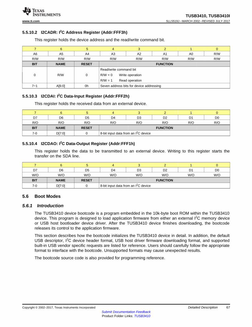
67
TUSB3410, TUSB3410Iwww.ti.com SLLS519J –MARCH 2002–REVISED JULY 2017
Submit Documentation FeedbackProduct Folder Links: TUSB3410
Detailed DescriptionCopyright © 2002–2017, Texas Instruments Incorporated
5.5.10.2 I2CADR: I2C Address Register (Addr:FFF3h)
This register holds the device address and the read/write command bit.
7 6 5 4 3 2 1 0A6 A5 A4 A3 A2 A1 A0 R/W
R/W R/W R/W R/W R/W R/W R/W R/WBIT NAME RESET FUNCTION
0 R/W 0Read/write command bitR/W = 0 Write operationR/W = 1 Read operation
7−1 A[6:0] 0h Seven address bits for device addressing
5.5.10.3 I2CDAI: I2C Data-Input Register (Addr:FFF2h)
This register holds the received data from an external device.
7 6 5 4 3 2 1 0D7 D6 D5 D4 D3 D2 D1 D0R/O R/O R/O R/O R/O R/O R/O R/OBIT NAME RESET FUNCTION7-0 D[7:0] 0 8-bit input data from an I2C device
5.5.10.4 I2CDAO: I2C Data-Output Register (Addr:FFF1h)
This register holds the data to be transmitted to an external device. Writing to this register starts thetransfer on the SDA line.
7 6 5 4 3 2 1 0D7 D6 D5 D4 D3 D2 D1 D0
W/O W/O W/O W/O W/O W/O W/O W/OBIT NAME RESET FUNCTION7-0 D[7:0] 0 8-bit input data from an I2C device
5.6 Boot Modes
5.6.1 IntroductionThe TUSB3410 device bootcode is a program embedded in the 10k-byte boot ROM within the TUSB3410device. This program is designed to load application firmware from either an external I2C memory deviceor USB host bootloader device driver. After the TUSB3410 device finishes downloading, the bootcodereleases its control to the application firmware.
This section describes how the bootcode initializes the TUSB3410 device in detail. In addition, the defaultUSB descriptor, I2C device header format, USB host driver firmware downloading format, and supportedbuilt-in USB vendor specific requests are listed for reference. Users should carefully follow the appropriateformat to interface with the bootcode. Unsupported formats may cause unexpected results.
The bootcode source code is also provided for programming reference.

68
TUSB3410, TUSB3410ISLLS519J –MARCH 2002–REVISED JULY 2017 www.ti.com
Submit Documentation FeedbackProduct Folder Links: TUSB3410
Detailed Description Copyright © 2002–2017, Texas Instruments Incorporated
5.6.2 Bootcode Programming FlowAfter power-on reset, the bootcode initializes the I2C and USB registers along with internal variables. Thebootcode then checks to see if an I2C device is present and contains a valid signature. If an I2C device ispresent and contains a valid signature, the bootcode continues searching for descriptor blocks and thenprocesses them if the checksum is correct. If application firmware was found, then the bootcodedownloads it and releases the control to the application firmware. Otherwise, the bootcode connects to theUSB and waits for host driver to download application firmware. Once firmware downloading is complete,the bootcode releases the control to the firmware.
The following is the bootcode step-by-step operation.• Check if bootcode is in the application mode. This is the mode that is entered after application code is
downloaded through either an I2C device or the USB. If the bootcode is in the application mode, thenthe bootcode releases the control to the application firmware. Otherwise, the bootcode continues.
• Initialize all the default settings.– Call CopyDefaultSettings() routine.
Set I2C to 400-kHz speed.– Call UsbDataInitialization() routine.
Set bFUNADR = 0Disconnect from USB (bUSBCTL = 0x00)Bootcode handles USB resetCopy predefined device, configuration, and string descriptors to RAMDisable all endpoints and enable USB interrupts (SETUP, RSTR, SUSR, and RESR)
• Search for product signature– Check if valid signature is in I2C. If not, skip the I2C process.
Read 2 bytes from address 0x0000 with type III and device address 0. Stop searching if validsignature is found.Read 2 bytes from address 0x0000 with type II and device address 4. Stop searching if validsignature is found.
• If a valid I2C signature is found, then load the customized device, configuration and string descriptorsfrom I2C EEPROM.– Process each descriptor block from I2C until end of header is found
If the descriptor block contains device, configuration, or string descriptors, then the bootcodeoverwrites the default descriptors.If the descriptor block contains binary firmware, then the bootcode sets the header pointer to thebeginning of the binary firmware in the I2C EEPROM.If the descriptor block is end of header, then the bootcode stops searching.
• Enable global and USB interrupts and set the connection bit to 1.– Enable global interrupts by setting bit 7 (EA) within the SIE register (see Section 5.5.9.1.1) to 1.– Enable all internal peripheral interrupts by setting the EX0 bit within the SIE register to 1.– Connect to the USB by setting bit 7 (CONT) within the USBCNTL register (see Section 5.5.5.4) to
1.

69
TUSB3410, TUSB3410Iwww.ti.com SLLS519J –MARCH 2002–REVISED JULY 2017
Submit Documentation FeedbackProduct Folder Links: TUSB3410
Detailed DescriptionCopyright © 2002–2017, Texas Instruments Incorporated
• Wait for any interrupt events until Get DEVICE DESCIPTOR setup packet arrives.– Suspend interrupt
The idle bit in the MCU PCON register is set and suspend mode is entered. USB reset wakes upthe microcontroller.
– Resume interruptBootcode wakes up and waits for new USB requests.
– Reset interruptCall UsbReset() routine.
– Setup interruptBootcode processes the request.
– USB reboot requestDisconnect from the USB by clearing bit 7 (CONT) in the USBCTL register and restart at address0x0000.
• Download firmware from I2C EEPROM– Disable global interrupts by clearing bit 7 (EA) within the SIE register– Load firmware to XDATA space if available.
• Download firmware from the USB.– If no firmware is found in an I2C EEPROM, the USB host downloads firmware through output
endpoint 1.– In the first data packet to output endpoint 1, the USB host driver adds 3 bytes before the application
firmware in binary format. These three bytes are the LSB and MSB indicating the firmware size andfollowed by the arithmetic checksum of the binary firmware.
• Release control to the application firmware.– Update the USB configuration and interface number.– Release control to application firmware.
• Application firmware– Either disconnect from the USB or continue responding to USB requests.
5.6.3 Default Bootcode SettingsThe bootcode has its own predefined device, configuration, and string descriptors. These defaultdescriptors should be used in evaluation only. They must not be used in the end-user product.
5.6.3.1 Device Descriptor
The device descriptor provides the USB version that the device supports, device class, protocol, vendorand product identifications, strings, and number of possible configurations. The operation system(Windows, MAC, or Linux) reads this descriptor to decide which device driver should be used tocommunicate with this device.
The bootcode uses 0x0451 (Texas Instruments) as the vendor ID and 0x3410 (TUSB3410) as the productID. It also supports three different strings and one configuration. Table 5-16 lists the device descriptor.
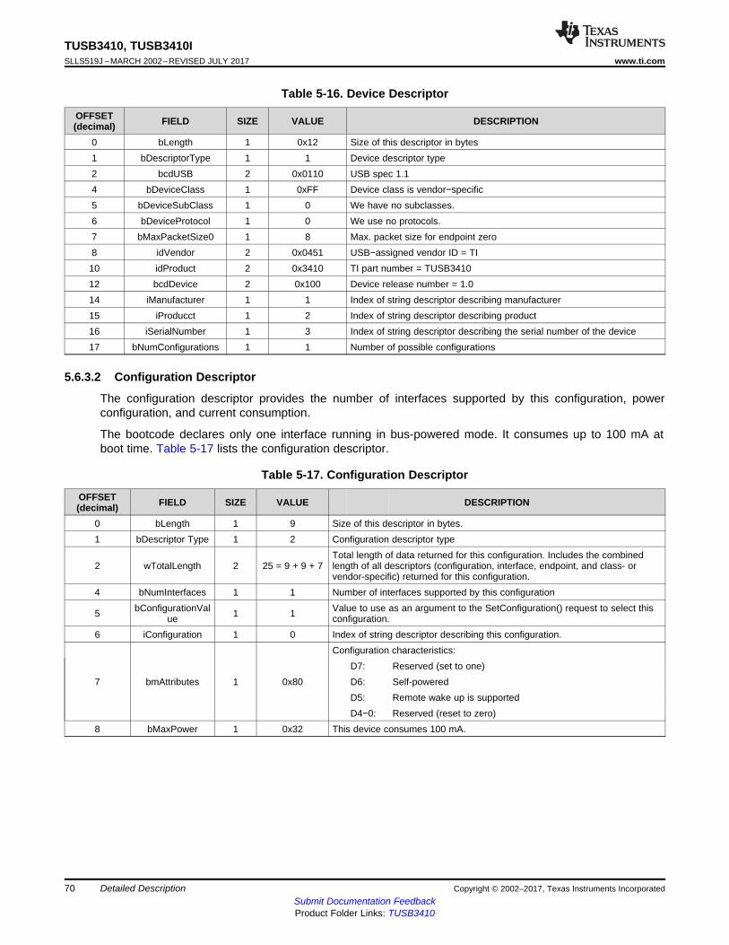
70
TUSB3410, TUSB3410ISLLS519J –MARCH 2002–REVISED JULY 2017 www.ti.com
Submit Documentation FeedbackProduct Folder Links: TUSB3410
Detailed Description Copyright © 2002–2017, Texas Instruments Incorporated
Table 5-16. Device Descriptor
OFFSET(decimal) FIELD SIZE VALUE DESCRIPTION
0 bLength 1 0x12 Size of this descriptor in bytes1 bDescriptorType 1 1 Device descriptor type2 bcdUSB 2 0x0110 USB spec 1.14 bDeviceClass 1 0xFF Device class is vendor−specific5 bDeviceSubClass 1 0 We have no subclasses.6 bDeviceProtocol 1 0 We use no protocols.7 bMaxPacketSize0 1 8 Max. packet size for endpoint zero8 idVendor 2 0x0451 USB−assigned vendor ID = TI10 idProduct 2 0x3410 TI part number = TUSB341012 bcdDevice 2 0x100 Device release number = 1.014 iManufacturer 1 1 Index of string descriptor describing manufacturer15 iProducct 1 2 Index of string descriptor describing product16 iSerialNumber 1 3 Index of string descriptor describing the serial number of the device17 bNumConfigurations 1 1 Number of possible configurations
5.6.3.2 Configuration Descriptor
The configuration descriptor provides the number of interfaces supported by this configuration, powerconfiguration, and current consumption.
The bootcode declares only one interface running in bus-powered mode. It consumes up to 100 mA atboot time. Table 5-17 lists the configuration descriptor.
Table 5-17. Configuration Descriptor
OFFSET(decimal) FIELD SIZE VALUE DESCRIPTION
0 bLength 1 9 Size of this descriptor in bytes.1 bDescriptor Type 1 2 Configuration descriptor type
2 wTotalLength 2 25 = 9 + 9 + 7Total length of data returned for this configuration. Includes the combinedlength of all descriptors (configuration, interface, endpoint, and class- orvendor-specific) returned for this configuration.
4 bNumInterfaces 1 1 Number of interfaces supported by this configuration
5 bConfigurationValue 1 1 Value to use as an argument to the SetConfiguration() request to select this
configuration.6 iConfiguration 1 0 Index of string descriptor describing this configuration.
7 bmAttributes 1 0x80
Configuration characteristics:D7: Reserved (set to one)D6: Self-poweredD5: Remote wake up is supportedD4−0: Reserved (reset to zero)
8 bMaxPower 1 0x32 This device consumes 100 mA.
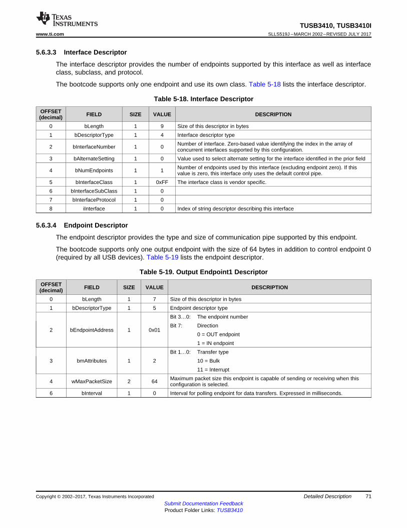
71
TUSB3410, TUSB3410Iwww.ti.com SLLS519J –MARCH 2002–REVISED JULY 2017
Submit Documentation FeedbackProduct Folder Links: TUSB3410
Detailed DescriptionCopyright © 2002–2017, Texas Instruments Incorporated
5.6.3.3 Interface Descriptor
The interface descriptor provides the number of endpoints supported by this interface as well as interfaceclass, subclass, and protocol.
The bootcode supports only one endpoint and use its own class. Table 5-18 lists the interface descriptor.
Table 5-18. Interface Descriptor
OFFSET(decimal) FIELD SIZE VALUE DESCRIPTION
0 bLength 1 9 Size of this descriptor in bytes1 bDescriptorType 1 4 Interface descriptor type
2 bInterfaceNumber 1 0 Number of interface. Zero-based value identifying the index in the array ofconcurrent interfaces supported by this configuration.
3 bAlternateSetting 1 0 Value used to select alternate setting for the interface identified in the prior field
4 bNumEndpoints 1 1 Number of endpoints used by this interface (excluding endpoint zero). If thisvalue is zero, this interface only uses the default control pipe.
5 bInterfaceClass 1 0xFF The interface class is vendor specific.6 bInterfaceSubClass 1 07 bInterfaceProtocol 1 08 iInterface 1 0 Index of string descriptor describing this interface
5.6.3.4 Endpoint Descriptor
The endpoint descriptor provides the type and size of communication pipe supported by this endpoint.
The bootcode supports only one output endpoint with the size of 64 bytes in addition to control endpoint 0(required by all USB devices). Table 5-19 lists the endpoint descriptor.
Table 5-19. Output Endpoint1 Descriptor
OFFSET(decimal) FIELD SIZE VALUE DESCRIPTION
0 bLength 1 7 Size of this descriptor in bytes1 bDescriptorType 1 5 Endpoint descriptor type
2 bEndpointAddress 1 0x01
Bit 3…0: The endpoint numberBit 7: Direction
0 = OUT endpoint1 = IN endpoint
3 bmAttributes 1 2Bit 1…0: Transfer type
10 = Bulk11 = Interrupt
4 wMaxPacketSize 2 64 Maximum packet size this endpoint is capable of sending or receiving when thisconfiguration is selected.
6 bInterval 1 0 Interval for polling endpoint for data transfers. Expressed in milliseconds.

72
TUSB3410, TUSB3410ISLLS519J –MARCH 2002–REVISED JULY 2017 www.ti.com
Submit Documentation FeedbackProduct Folder Links: TUSB3410
Detailed Description Copyright © 2002–2017, Texas Instruments Incorporated
5.6.3.5 String Descriptor
The string descriptor contains data in the Unicode format. It is used to show the manufacturers name,product model, and serial number in human readable format.
The bootcode supports three strings. The first string is the manufacturers name. The second string is theproduct name. The third string is the serial number. Table 5-20 lists the string descriptor.
Table 5-20. String Descriptor
OFFSET(decimal) FIELD SIZE VALUE DESCRIPTION
0 bLength 1 4 Size of string 0 descriptor in bytes1 bDescriptorType 1 0x03 String descriptor type2 wLANGID[0] 2 0x0409 English4 bLength 1 36 (decimal) Size of string 1 descriptor in bytes5 bDescriptorType 1 0x03 String descriptor type6 bString 2 T,0x00 Unicode, T is the first byte8 2 e,0x00 Texas Instruments10 2 x,0x0012 2 a,0x0014 2 s,0x0016 2 ‘ ’,0x0018 2 I,0x0020 2 n,0x0022 2 s,0x0024 2 t,0x0026 2 r,0x0028 2 u,0x0030 2 m,0x0032 2 e,0x0034 2 n,0x0036 2 t,0x0038 2 s,0x0040 bLength 1 42 (decimal) Size of string 2 descriptor in bytes41 bDescriptorType 1 0x03 STRING descriptor type42 bString 2 T,0x00 UNICODE, T is first byte44 2 U,0x00 TUSB3410 boot device46 2 S,0x0048 2 B,0x0050 2 3,0x0052 2 4,0x0054 2 1,0x0056 2 0,0x0058 2 ‘ ‘,0x0060 2 B,0x0062 2 o,0x0064 2 o,0x0066 2 t,0x0068 2 ‘ ’,0x0070 2 D,0x00
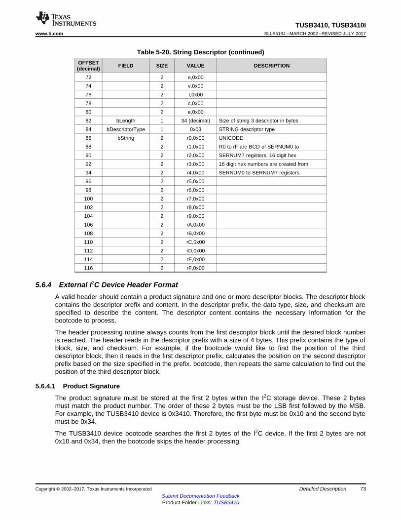
73
TUSB3410, TUSB3410Iwww.ti.com SLLS519J –MARCH 2002–REVISED JULY 2017
Submit Documentation FeedbackProduct Folder Links: TUSB3410
Detailed DescriptionCopyright © 2002–2017, Texas Instruments Incorporated
Table 5-20. String Descriptor (continued)OFFSET(decimal) FIELD SIZE VALUE DESCRIPTION
72 2 e,0x0074 2 v,0x0076 2 I,0x0078 2 c,0x0080 2 e,0x0082 bLength 1 34 (decimal) Size of string 3 descriptor in bytes84 bDescriptorType 1 0x03 STRING descriptor type86 bString 2 r0,0x00 UNICODE88 2 r1,0x00 R0 to rF are BCD of SERNUM0 to90 2 r2,0x00 SERNUM7 registers. 16 digit hex92 2 r3,0x00 16 digit hex numbers are created from94 2 r4,0x00 SERNUM0 to SERNUM7 registers96 2 r5,0x0098 2 r6,0x00100 2 r7,0x00102 2 r8,0x00104 2 r9,0x00106 2 rA,0x00108 2 rB,0x00110 2 rC,0x00112 2 rD,0x00114 2 rE,0x00116 2 rF,0x00
5.6.4 External I2C Device Header FormatA valid header should contain a product signature and one or more descriptor blocks. The descriptor blockcontains the descriptor prefix and content. In the descriptor prefix, the data type, size, and checksum arespecified to describe the content. The descriptor content contains the necessary information for thebootcode to process.
The header processing routine always counts from the first descriptor block until the desired block numberis reached. The header reads in the descriptor prefix with a size of 4 bytes. This prefix contains the type ofblock, size, and checksum. For example, if the bootcode would like to find the position of the thirddescriptor block, then it reads in the first descriptor prefix, calculates the position on the second descriptorprefix based on the size specified in the prefix. bootcode, then repeats the same calculation to find out theposition of the third descriptor block.
5.6.4.1 Product Signature
The product signature must be stored at the first 2 bytes within the I2C storage device. These 2 bytesmust match the product number. The order of these 2 bytes must be the LSB first followed by the MSB.For example, the TUSB3410 device is 0x3410. Therefore, the first byte must be 0x10 and the second bytemust be 0x34.
The TUSB3410 device bootcode searches the first 2 bytes of the I2C device. If the first 2 bytes are not0x10 and 0x34, then the bootcode skips the header processing.
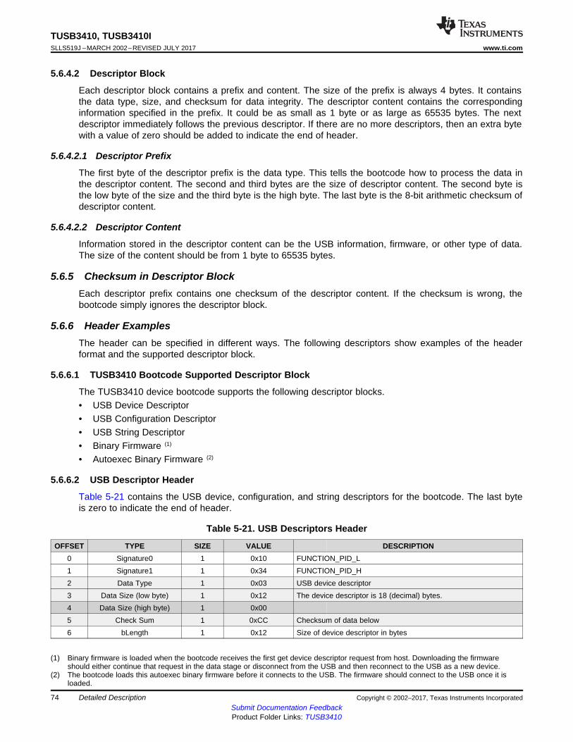
74
TUSB3410, TUSB3410ISLLS519J –MARCH 2002–REVISED JULY 2017 www.ti.com
Submit Documentation FeedbackProduct Folder Links: TUSB3410
Detailed Description Copyright © 2002–2017, Texas Instruments Incorporated
(1) Binary firmware is loaded when the bootcode receives the first get device descriptor request from host. Downloading the firmwareshould either continue that request in the data stage or disconnect from the USB and then reconnect to the USB as a new device.
(2) The bootcode loads this autoexec binary firmware before it connects to the USB. The firmware should connect to the USB once it isloaded.
5.6.4.2 Descriptor Block
Each descriptor block contains a prefix and content. The size of the prefix is always 4 bytes. It containsthe data type, size, and checksum for data integrity. The descriptor content contains the correspondinginformation specified in the prefix. It could be as small as 1 byte or as large as 65535 bytes. The nextdescriptor immediately follows the previous descriptor. If there are no more descriptors, then an extra bytewith a value of zero should be added to indicate the end of header.
5.6.4.2.1 Descriptor Prefix
The first byte of the descriptor prefix is the data type. This tells the bootcode how to process the data inthe descriptor content. The second and third bytes are the size of descriptor content. The second byte isthe low byte of the size and the third byte is the high byte. The last byte is the 8-bit arithmetic checksum ofdescriptor content.
5.6.4.2.2 Descriptor Content
Information stored in the descriptor content can be the USB information, firmware, or other type of data.The size of the content should be from 1 byte to 65535 bytes.
5.6.5 Checksum in Descriptor BlockEach descriptor prefix contains one checksum of the descriptor content. If the checksum is wrong, thebootcode simply ignores the descriptor block.
5.6.6 Header ExamplesThe header can be specified in different ways. The following descriptors show examples of the headerformat and the supported descriptor block.
5.6.6.1 TUSB3410 Bootcode Supported Descriptor Block
The TUSB3410 device bootcode supports the following descriptor blocks.• USB Device Descriptor• USB Configuration Descriptor• USB String Descriptor• Binary Firmware (1)
• Autoexec Binary Firmware (2)
5.6.6.2 USB Descriptor Header
Table 5-21 contains the USB device, configuration, and string descriptors for the bootcode. The last byteis zero to indicate the end of header.
Table 5-21. USB Descriptors Header
OFFSET TYPE SIZE VALUE DESCRIPTION0 Signature0 1 0x10 FUNCTION_PID_L1 Signature1 1 0x34 FUNCTION_PID_H2 Data Type 1 0x03 USB device descriptor3 Data Size (low byte) 1 0x12 The device descriptor is 18 (decimal) bytes.4 Data Size (high byte) 1 0x005 Check Sum 1 0xCC Checksum of data below6 bLength 1 0x12 Size of device descriptor in bytes
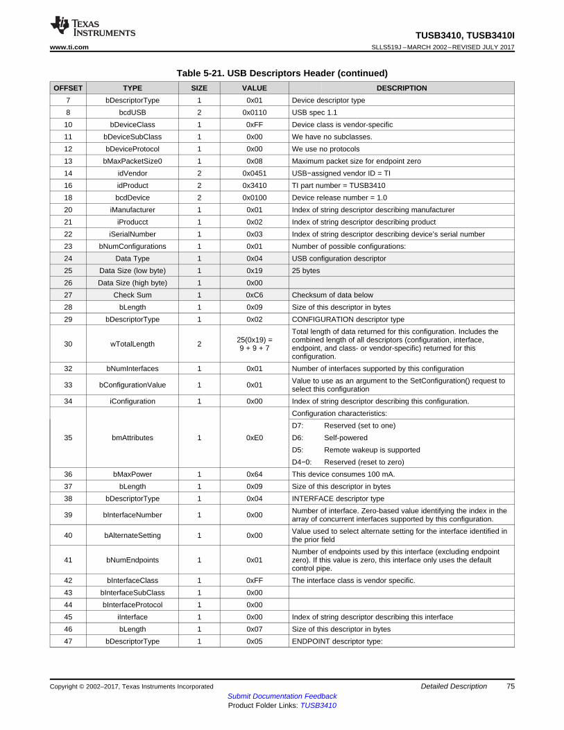
75
TUSB3410, TUSB3410Iwww.ti.com SLLS519J –MARCH 2002–REVISED JULY 2017
Submit Documentation FeedbackProduct Folder Links: TUSB3410
Detailed DescriptionCopyright © 2002–2017, Texas Instruments Incorporated
Table 5-21. USB Descriptors Header (continued)OFFSET TYPE SIZE VALUE DESCRIPTION
7 bDescriptorType 1 0x01 Device descriptor type8 bcdUSB 2 0x0110 USB spec 1.110 bDeviceClass 1 0xFF Device class is vendor-specific11 bDeviceSubClass 1 0x00 We have no subclasses.12 bDeviceProtocol 1 0x00 We use no protocols13 bMaxPacketSize0 1 0x08 Maximum packet size for endpoint zero14 idVendor 2 0x0451 USB−assigned vendor ID = TI16 idProduct 2 0x3410 TI part number = TUSB341018 bcdDevice 2 0x0100 Device release number = 1.020 iManufacturer 1 0x01 Index of string descriptor describing manufacturer21 iProducct 1 0x02 Index of string descriptor describing product22 iSerialNumber 1 0x03 Index of string descriptor describing device’s serial number23 bNumConfigurations 1 0x01 Number of possible configurations:24 Data Type 1 0x04 USB configuration descriptor25 Data Size (low byte) 1 0x19 25 bytes26 Data Size (high byte) 1 0x0027 Check Sum 1 0xC6 Checksum of data below28 bLength 1 0x09 Size of this descriptor in bytes29 bDescriptorType 1 0x02 CONFIGURATION descriptor type
30 wTotalLength 2 25(0x19) =9 + 9 + 7
Total length of data returned for this configuration. Includes thecombined length of all descriptors (configuration, interface,endpoint, and class- or vendor-specific) returned for thisconfiguration.
32 bNumInterfaces 1 0x01 Number of interfaces supported by this configuration
33 bConfigurationValue 1 0x01 Value to use as an argument to the SetConfiguration() request toselect this configuration
34 iConfiguration 1 0x00 Index of string descriptor describing this configuration.
35 bmAttributes 1 0xE0
Configuration characteristics:D7: Reserved (set to one)D6: Self-poweredD5: Remote wakeup is supportedD4−0: Reserved (reset to zero)
36 bMaxPower 1 0x64 This device consumes 100 mA.37 bLength 1 0x09 Size of this descriptor in bytes38 bDescriptorType 1 0x04 INTERFACE descriptor type
39 bInterfaceNumber 1 0x00 Number of interface. Zero-based value identifying the index in thearray of concurrent interfaces supported by this configuration.
40 bAlternateSetting 1 0x00 Value used to select alternate setting for the interface identified inthe prior field
41 bNumEndpoints 1 0x01Number of endpoints used by this interface (excluding endpointzero). If this value is zero, this interface only uses the defaultcontrol pipe.
42 bInterfaceClass 1 0xFF The interface class is vendor specific.43 bInterfaceSubClass 1 0x0044 bInterfaceProtocol 1 0x0045 iInterface 1 0x00 Index of string descriptor describing this interface46 bLength 1 0x07 Size of this descriptor in bytes47 bDescriptorType 1 0x05 ENDPOINT descriptor type:
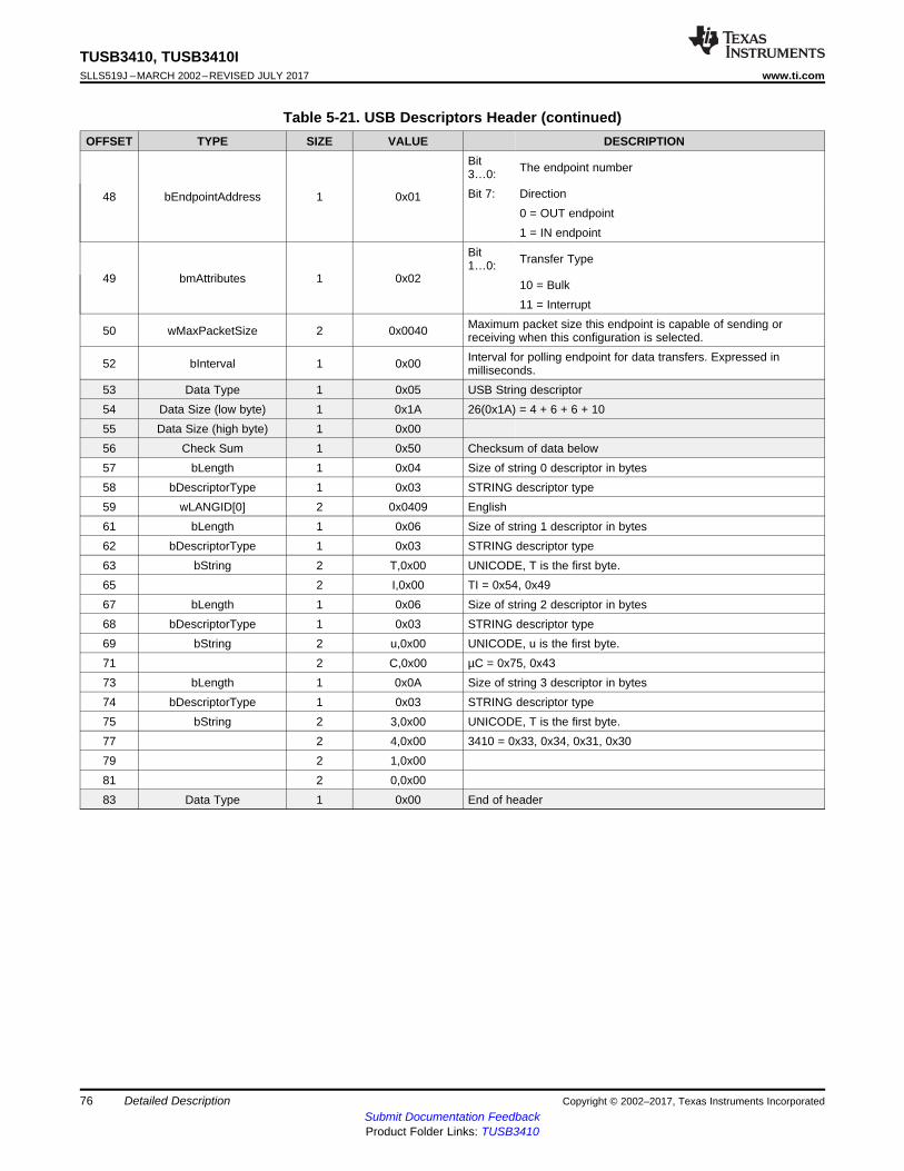
76
TUSB3410, TUSB3410ISLLS519J –MARCH 2002–REVISED JULY 2017 www.ti.com
Submit Documentation FeedbackProduct Folder Links: TUSB3410
Detailed Description Copyright © 2002–2017, Texas Instruments Incorporated
Table 5-21. USB Descriptors Header (continued)OFFSET TYPE SIZE VALUE DESCRIPTION
48 bEndpointAddress 1 0x01
Bit3…0: The endpoint number
Bit 7: Direction0 = OUT endpoint1 = IN endpoint
49 bmAttributes 1 0x02
Bit1…0: Transfer Type
10 = Bulk11 = Interrupt
50 wMaxPacketSize 2 0x0040 Maximum packet size this endpoint is capable of sending orreceiving when this configuration is selected.
52 bInterval 1 0x00 Interval for polling endpoint for data transfers. Expressed inmilliseconds.
53 Data Type 1 0x05 USB String descriptor54 Data Size (low byte) 1 0x1A 26(0x1A) = 4 + 6 + 6 + 1055 Data Size (high byte) 1 0x0056 Check Sum 1 0x50 Checksum of data below57 bLength 1 0x04 Size of string 0 descriptor in bytes58 bDescriptorType 1 0x03 STRING descriptor type59 wLANGID[0] 2 0x0409 English61 bLength 1 0x06 Size of string 1 descriptor in bytes62 bDescriptorType 1 0x03 STRING descriptor type63 bString 2 T,0x00 UNICODE, T is the first byte.65 2 I,0x00 TI = 0x54, 0x4967 bLength 1 0x06 Size of string 2 descriptor in bytes68 bDescriptorType 1 0x03 STRING descriptor type69 bString 2 u,0x00 UNICODE, u is the first byte.71 2 C,0x00 µC = 0x75, 0x4373 bLength 1 0x0A Size of string 3 descriptor in bytes74 bDescriptorType 1 0x03 STRING descriptor type75 bString 2 3,0x00 UNICODE, T is the first byte.77 2 4,0x00 3410 = 0x33, 0x34, 0x31, 0x3079 2 1,0x0081 2 0,0x0083 Data Type 1 0x00 End of header
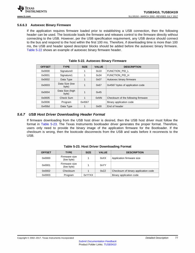
77
TUSB3410, TUSB3410Iwww.ti.com SLLS519J –MARCH 2002–REVISED JULY 2017
Submit Documentation FeedbackProduct Folder Links: TUSB3410
Detailed DescriptionCopyright © 2002–2017, Texas Instruments Incorporated
5.6.6.3 Autoexec Binary Firmware
If the application requires firmware loaded prior to establishing a USB connection, then the followingheader can be used. The bootcode loads the firmware and releases control to the firmware directly withoutconnecting to the USB. However, per the USB specification requirement, any USB device should connectto the bus and respond to the host within the first 100 ms. Therefore, if downloading time is more than 100ms, the USB and header speed descriptor blocks should be added before the autoexec binary firmware.Table 5-22 shows an example of autoexec binary firmware header.
Table 5-22. Autoexec Binary Firmware
OFFSET TYPE SIZE VALUE DESCRIPTION0x0000 Signature0 1 0x10 FUNCTION_PID_L0x0001 Signature1 1 0x34 FUNCTION_PID_H0x0002 Data Type 1 0x07 Autoexec binary firmware
0x0003 Data Size (lowbyte) 1 0x67 0x4567 bytes of application code
0x0004 Data Size (highbyte) 1 0x45
0x0005 Check Sum 1 0xNN Checksum of the following firmware0x0006 Program 0x4567 Binary application code0x456d Data Type 1 0x00 End of header
5.6.7 USB Host Driver Downloading Header FormatIf firmware downloading from the USB host driver is desired, then the USB host driver must follow theformat in Table 5-23. The Texas Instruments bootloader driver generates the proper format. Therefore,users only need to provide the binary image of the application firmware for the Bootloader. If thechecksum is wrong, then the bootcode disconnects from the USB and waits before it reconnects to theUSB.
Table 5-23. Host Driver Downloading Format
OFFSET TYPE SIZE VALUE DESCRIPTION
0x0000 Firmware size(low byte) 1 0xXX Application firmware size
0x0001 Firmware size(low byte) 1 0xYY
0x0002 Checksum 1 0xZZ Checksum of binary application code0x0003 Program 0xYYXX Binary application code
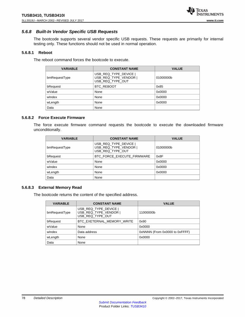
78
TUSB3410, TUSB3410ISLLS519J –MARCH 2002–REVISED JULY 2017 www.ti.com
Submit Documentation FeedbackProduct Folder Links: TUSB3410
Detailed Description Copyright © 2002–2017, Texas Instruments Incorporated
5.6.8 Built-In Vendor Specific USB RequestsThe bootcode supports several vendor specific USB requests. These requests are primarily for internaltesting only. These functions should not be used in normal operation.
5.6.8.1 Reboot
The reboot command forces the bootcode to execute.
VARIABLE CONSTANT NAME VALUE
bmRequestTypeUSB_REQ_TYPE_DEVICE |USB_REQ_TYPE_VENDOR |USB_REQ_TYPE_OUT
01000000b
bRequest BTC_REBOOT 0x85wValue None 0x0000wIndex None 0x0000wLength None 0x0000Data None
5.6.8.2 Force Execute Firmware
The force execute firmware command requests the bootcode to execute the downloaded firmwareunconditionally.
VARIABLE CONSTANT NAME VALUE
bmRequestTypeUSB_REQ_TYPE_DEVICE |USB_REQ_TYPE_VENDOR |USB_REQ_TYPE_OUT
01000000b
bRequest BTC_FORCE_EXECUTE_FIRMWARE 0x8FwValue None 0x0000wIndex None 0x0000wLength None 0x0000Data None
5.6.8.3 External Memory Read
The bootcode returns the content of the specified address.
VARIABLE CONSTANT NAME VALUE
bmRequestTypeUSB_REQ_TYPE_DEVICE |USB_REQ_TYPE_VENDOR |USB_REQ_TYPE_OUT
11000000b
bRequest BTC_EXETERNAL_MEMORY_WRITE 0x90wValue None 0x0000wIndex Data address 0xNNNN (From 0x0000 to 0xFFFF)wLength None 0x0000Data None
79
TUSB3410, TUSB3410Iwww.ti.com SLLS519J –MARCH 2002–REVISED JULY 2017
Submit Documentation FeedbackProduct Folder Links: TUSB3410
Detailed DescriptionCopyright © 2002–2017, Texas Instruments Incorporated
5.6.8.4 External Memory Write
The external memory write command tells the bootcode to write data to the specified address.
VARIABLE CONSTANT NAME VALUE
bmRequestTypeUSB_REQ_TYPE_DEVICE |USB_REQ_TYPE_VENDOR |USB_REQ_TYPE_OUT
01000000b
bRequest BTC_EXETERNAL_MEMORY_WRITE 0x91
wValue HI: 0x00LO: Data 0x00NN
wIndex Data address 0xNNNN (From 0x0000 to 0xFFFF)wLength None 0x0000Data None
5.6.8.5 I2C Memory Read
The bootcode returns the content of the specified address in I2C EEPROM.
In the wValue field, the I2C device number is from 0x00 to 0x07 in the high byte. The memory type is from0x01 to 0x03 for CAT I to CAT III devices. If bit 7 of bValueL is set, then the bus speed is 400 kHz. Thisrequest is also used to set the device number and speed before the I2C write request.
VARIABLE CONSTANT NAME VALUE
bmRequestTypeUSB_REQ_TYPE_DEVICE |USB_REQ_TYPE_VENDOR |USB_REQ_TYPE_OUT
11000000b
bRequest BTC_I2C_MEMORY_READ 0x92
wValue HI:LO:
I2C device numberMemory type bit[1:0]Speed bit[7]
0xXXYY
wIndex Data address 0xNNNN (From 0x0000 to 0xFFFF)wLength 1 byte 0x0001Data Byte in the specified address 0xNN
80
TUSB3410, TUSB3410ISLLS519J –MARCH 2002–REVISED JULY 2017 www.ti.com
Submit Documentation FeedbackProduct Folder Links: TUSB3410
Detailed Description Copyright © 2002–2017, Texas Instruments Incorporated
5.6.8.6 I2C Memory Write
The I2C memory write command tells the bootcode to write data to the specified address.
VARIABLE CONSTANT NAME VALUE
bmRequestTypeUSB_REQ_TYPE_DEVICE |USB_REQ_TYPE_VENDOR |USB_REQ_TYPE_OUT
01000000b
bRequest BTC_I2C_MEMORY_WRITE 0x93
wValue HI: should be zeroLO: Data 0x00NN
wIndex Data address 0xNNNN (From 0x0000 to 0xFFFF)wLength None 0x0000Data None
5.6.8.7 Internal ROM Memory Read
The bootcode returns the byte of the specified address within the boot ROM. That is, the binary code ofthe bootcode.
VARIABLE CONSTANT NAME VALUE
bmRequestTypeUSB_REQ_TYPE_DEVICE |USB_REQ_TYPE_VENDOR |USB_REQ_TYPE_OUT
01000000b
bRequest BTC_INTERNAL_ROM_MEMORY_READ 0x94
wValue None 0x0000wIndex Data address 0xNNNN (From 0x0000 to 0xFFFF)wLength 1 byte 0x0001Data Byte in the specified address 0xNN
5.6.9 Bootcode Programming Consideration
5.6.9.1 USB Requests
For each USB request, the bootcode follows these steps to ensure proper operation of the hardware:1. Determine the direction of the request by checking the MSB of the bmRequestType field and set the
DIR bit within the USBCTL register accordingly.2. Decode the command3. If another setup is pending, then return. Otherwise, serve the request.4. Check again, if another setup is pending then go to step 2.5. Clear the interrupt source and then the VECINT register.6. Exit the interrupt routine.
5.6.9.1.1 USB Request Transfers
The USB request consist of three types of transfers. They are control-read-with-data-stage, control-write-without-data-stage, and control-write-with-data-stage transfer. In each transfer, arrows indicate interruptsgenerated after receiving the setup packet, in or out token.

Setup Stage Data Stage StatusStage
Setup (0) IN(1) IN(0)More
PacketsIN(0/1) OUT(1)
INT INT INT INT
1.Hardware generates interrupt
to MCU.
2.Hardware sets NAK on both
the IN and the OUT endpoints.
3.Set DIR bit in USBCTL to
indicate the data direction.
4.Decode the setup packet.
5.If another setup packet
arrives, abandon this one.
6.Execute appropriate routine perTable 11-9.a) Clear NAK bit in OUT
endpoint.
b) Copy data to IN endpoint
buffer and set byte count.
1.Hardware generates interrupt to
MCU.
2.Copy data to IN buffer.
3.Clear the NAK bit.
4.If all data has been sent, stall input
endpoint.
1.Hardware does NOT generate
interrupt to MCU.
81
TUSB3410, TUSB3410Iwww.ti.com SLLS519J –MARCH 2002–REVISED JULY 2017
Submit Documentation FeedbackProduct Folder Links: TUSB3410
Detailed DescriptionCopyright © 2002–2017, Texas Instruments Incorporated
Figure 5-13 and Figure 5-14 show the USB data flow and how the hardware and firmware respond to theUSB requests. Table 5-24 and Table 5-25 lists the bootcode reposes to the standard USB requests.
Figure 5-13. Control Read Transfer
Table 5-24. Bootcode Response to Control Read Transfer
CONTROL READ ACTION IN BOOTCODEGet status of device Return power and remote wake-up settingsGet status of interface Return 2 bytes of zerosGet status of endpoint Return endpoint statusGet descriptor of device Return device descriptorGet descriptor of configuration Return configuration descriptorGet descriptor of string Return string descriptorGet descriptor of interface StallGet descriptor of endpoint StallGet configuration Return bConfiguredNumber valueGet interface Return bInterfaceNumber value
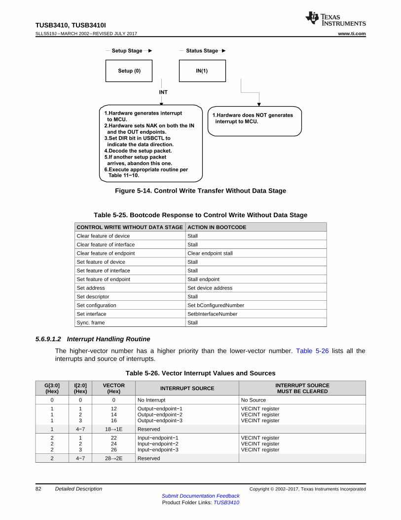
Setup Stage Status Stage
Setup (0) IN(1)
INT
1.Hardware generates interrupt
to MCU.
2.Hardware sets NAK on both the IN
and the OUT endpoints.
3.Set DIR bit in USBCTL to
indicate the data direction.
4.Decode the setup packet.
5.If another setup packet
arrives, abandon this one.
6.Execute appropriate routine perTable 11−10.
1.Hardware does NOT generates
interrupt to MCU.
82
TUSB3410, TUSB3410ISLLS519J –MARCH 2002–REVISED JULY 2017 www.ti.com
Submit Documentation FeedbackProduct Folder Links: TUSB3410
Detailed Description Copyright © 2002–2017, Texas Instruments Incorporated
Figure 5-14. Control Write Transfer Without Data Stage
Table 5-25. Bootcode Response to Control Write Without Data Stage
CONTROL WRITE WITHOUT DATA STAGE ACTION IN BOOTCODEClear feature of device StallClear feature of interface StallClear feature of endpoint Clear endpoint stallSet feature of device StallSet feature of interface StallSet feature of endpoint Stall endpointSet address Set device addressSet descriptor StallSet configuration Set bConfiguredNumberSet interface SetbInterfaceNumberSync. frame Stall
5.6.9.1.2 Interrupt Handling Routine
The higher-vector number has a higher priority than the lower-vector number. Table 5-26 lists all theinterrupts and source of interrupts.
Table 5-26. Vector Interrupt Values and Sources
G[3:0](Hex)
I[2:0](Hex)
VECTOR(Hex) INTERRUPT SOURCE INTERRUPT SOURCE
MUST BE CLEARED0 0 0 No Interrupt No Source111
123
121416
Output−endpoint−1Output−endpoint−2Output−endpoint−3
VECINT registerVECINT registerVECINT register
1 4−7 18→1E Reserved222
123
222426
Input−endpoint−1Input−endpoint−2Input−endpoint−3
VECINT registerVECINT registerVECINT register
2 4−7 28→2E Reserved
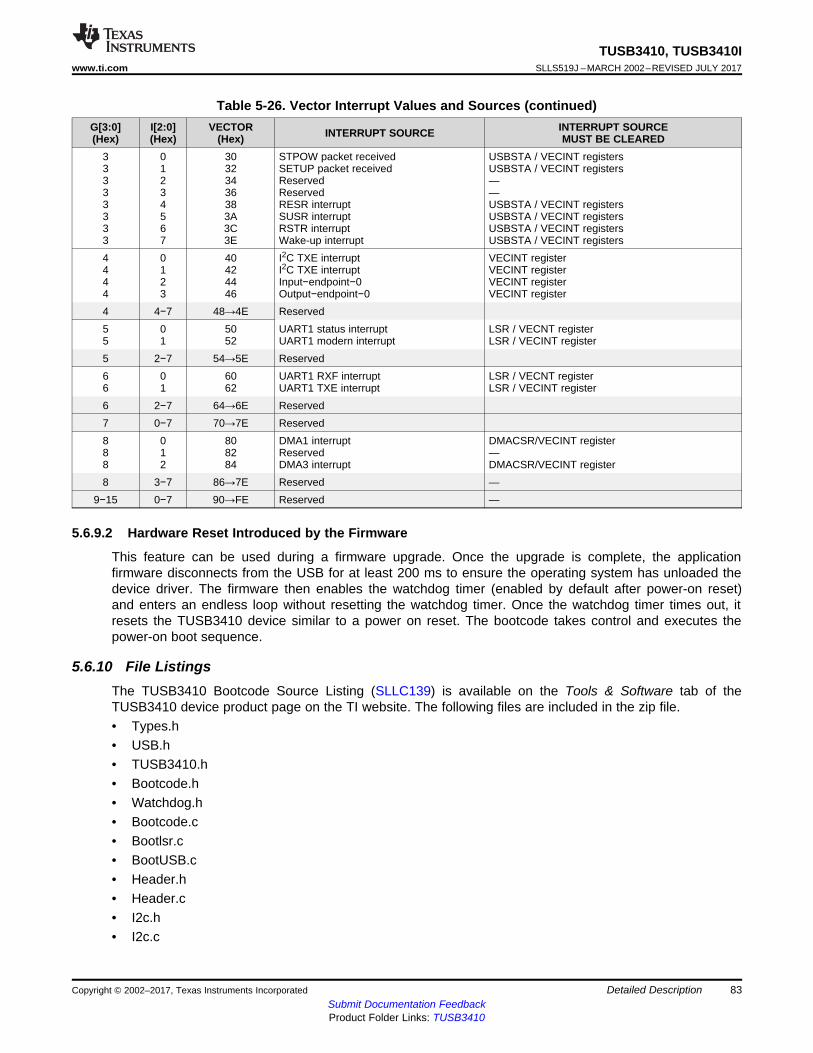
83
TUSB3410, TUSB3410Iwww.ti.com SLLS519J –MARCH 2002–REVISED JULY 2017
Submit Documentation FeedbackProduct Folder Links: TUSB3410
Detailed DescriptionCopyright © 2002–2017, Texas Instruments Incorporated
Table 5-26. Vector Interrupt Values and Sources (continued)G[3:0](Hex)
I[2:0](Hex)
VECTOR(Hex) INTERRUPT SOURCE INTERRUPT SOURCE
MUST BE CLEARED33333333
01234567
30323436383A3C3E
STPOW packet receivedSETUP packet receivedReservedReservedRESR interruptSUSR interruptRSTR interruptWake-up interrupt
USBSTA / VECINT registersUSBSTA / VECINT registers——USBSTA / VECINT registersUSBSTA / VECINT registersUSBSTA / VECINT registersUSBSTA / VECINT registers
4444
0123
40424446
I2C TXE interruptI2C TXE interruptInput−endpoint−0Output−endpoint−0
VECINT registerVECINT registerVECINT registerVECINT register
4 4−7 48→4E Reserved55
01
5052
UART1 status interruptUART1 modern interrupt
LSR / VECNT registerLSR / VECINT register
5 2−7 54→5E Reserved66
01
6062
UART1 RXF interruptUART1 TXE interrupt
LSR / VECNT registerLSR / VECINT register
6 2−7 64→6E Reserved7 0−7 70→7E Reserved888
012
808284
DMA1 interruptReservedDMA3 interrupt
DMACSR/VECINT register—DMACSR/VECINT register
8 3−7 86→7E Reserved —9−15 0−7 90→FE Reserved —
5.6.9.2 Hardware Reset Introduced by the Firmware
This feature can be used during a firmware upgrade. Once the upgrade is complete, the applicationfirmware disconnects from the USB for at least 200 ms to ensure the operating system has unloaded thedevice driver. The firmware then enables the watchdog timer (enabled by default after power-on reset)and enters an endless loop without resetting the watchdog timer. Once the watchdog timer times out, itresets the TUSB3410 device similar to a power on reset. The bootcode takes control and executes thepower-on boot sequence.
5.6.10 File ListingsThe TUSB3410 Bootcode Source Listing (SLLC139) is available on the Tools & Software tab of theTUSB3410 device product page on the TI website. The following files are included in the zip file.• Types.h• USB.h• TUSB3410.h• Bootcode.h• Watchdog.h• Bootcode.c• Bootlsr.c• BootUSB.c• Header.h• Header.c• I2c.h• I2c.c
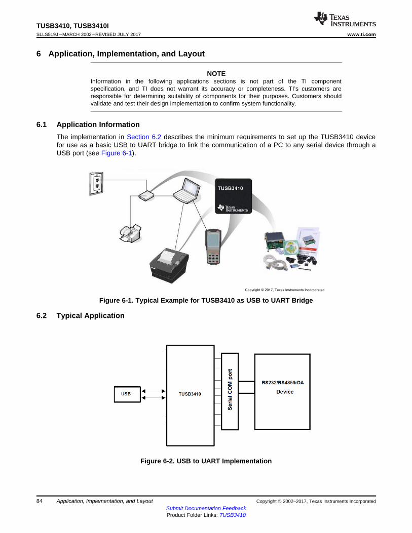
Copyright © 2017, Texas Instruments Incorporated
84
TUSB3410, TUSB3410ISLLS519J –MARCH 2002–REVISED JULY 2017 www.ti.com
Submit Documentation FeedbackProduct Folder Links: TUSB3410
Application, Implementation, and Layout Copyright © 2002–2017, Texas Instruments Incorporated
6 Application, Implementation, and Layout
NOTEInformation in the following applications sections is not part of the TI componentspecification, and TI does not warrant its accuracy or completeness. TI’s customers areresponsible for determining suitability of components for their purposes. Customers shouldvalidate and test their design implementation to confirm system functionality.
6.1 Application InformationThe implementation in Section 6.2 describes the minimum requirements to set up the TUSB3410 devicefor use as a basic USB to UART bridge to link the communication of a PC to any serial device through aUSB port (see Figure 6-1).
Figure 6-1. Typical Example for TUSB3410 as USB to UART Bridge
6.2 Typical Application
Figure 6-2. USB to UART Implementation
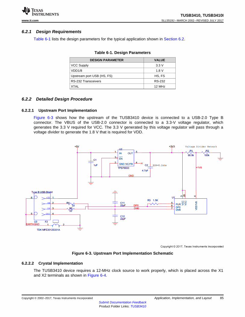
85
TUSB3410, TUSB3410Iwww.ti.com SLLS519J –MARCH 2002–REVISED JULY 2017
Submit Documentation FeedbackProduct Folder Links: TUSB3410
Application, Implementation, and LayoutCopyright © 2002–2017, Texas Instruments Incorporated
6.2.1 Design RequirementsTable 6-1 lists the design parameters for the typical application shown in Section 6.2.
Table 6-1. Design Parameters
DESIGN PARAMETER VALUEVCC Supply 3.3 VVDD1/8 1.8 VUpstream port USB (HS, FS) HS, FSRS-232 Transceivers RS-232XTAL 12 MHz
6.2.2 Detailed Design Procedure
6.2.2.1 Upstream Port Implementation
Figure 6-3 shows how the upstream of the TUSB3410 device is connected to a USB-2.0 Type Bconnector. The VBUS of the USB-2.0 connector is connected to a 3.3-V voltage regulator, whichgenerates the 3.3 V required for VCC. The 3.3 V generated by this voltage regulator will pass through avoltage divider to generate the 1.8 V that is required for VDD.
Figure 6-3. Upstream Port Implementation Schematic
6.2.2.2 Crystal Implementation
The TUSB3410 device requires a 12-MHz clock source to work properly, which is placed across the X1and X2 terminals as shown in Figure 6-4.
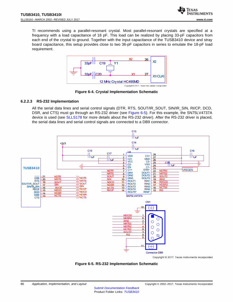
86
TUSB3410, TUSB3410ISLLS519J –MARCH 2002–REVISED JULY 2017 www.ti.com
Submit Documentation FeedbackProduct Folder Links: TUSB3410
Application, Implementation, and Layout Copyright © 2002–2017, Texas Instruments Incorporated
TI recommends using a parallel-resonant crystal. Most parallel-resonant crystals are specified at afrequency with a load capacitance of 18 pF. This load can be realized by placing 33-pF capacitors fromeach end of the crystal to ground. Together with the input capacitance of the TUSB3410 device and strayboard capacitance, this setup provides close to two 36-pF capacitors in series to emulate the 18-pF loadrequirement.
Figure 6-4. Crystal Implementation Schematic
6.2.2.3 RS-232 Implementation
All the serial data lines and serial control signals (DTR, RTS, SOUT/IR_SOUT, SIN/IR_SIN, RI/CP, DCD,DSR, and CTS) must go through an RS-232 driver (see Figure 6-5). For this example, the SN75LV4737Adevice is used (see SLLS178 for more details about the RS-232 driver). After the RS-232 driver is placed,the serial data lines and serial control signals are connected to a DB9 connector.
Figure 6-5. RS-232 Implementation Schematic
87
TUSB3410, TUSB3410Iwww.ti.com SLLS519J –MARCH 2002–REVISED JULY 2017
Submit Documentation FeedbackProduct Folder Links: TUSB3410
Application, Implementation, and LayoutCopyright © 2002–2017, Texas Instruments Incorporated
6.2.2.4 TUSB3410 Power Implementation
Figure 6-6 shows the power implementation for the TUSB3410 device.
Figure 6-6. Power Implementation
6.2.3 Application Performance Plot
Figure 6-7. High-Speed Upstream Port
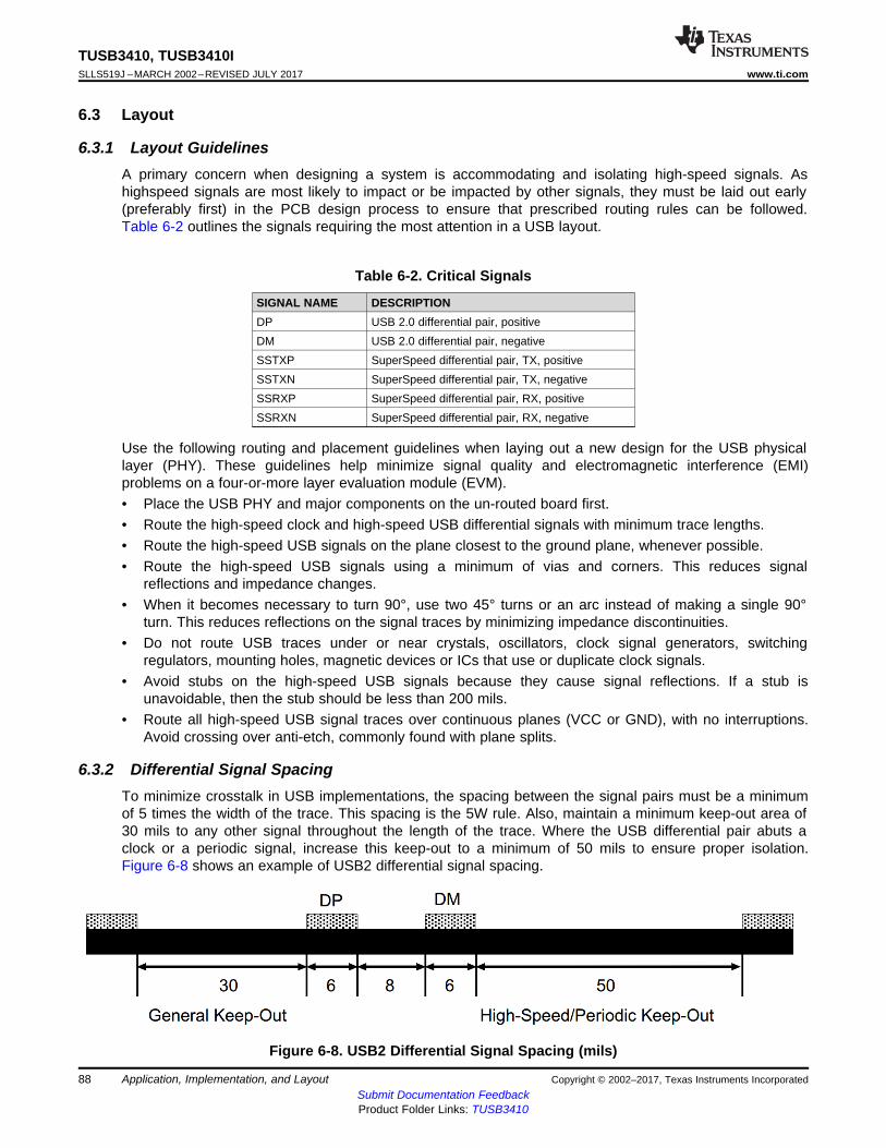
88
TUSB3410, TUSB3410ISLLS519J –MARCH 2002–REVISED JULY 2017 www.ti.com
Submit Documentation FeedbackProduct Folder Links: TUSB3410
Application, Implementation, and Layout Copyright © 2002–2017, Texas Instruments Incorporated
6.3 Layout
6.3.1 Layout GuidelinesA primary concern when designing a system is accommodating and isolating high-speed signals. Ashighspeed signals are most likely to impact or be impacted by other signals, they must be laid out early(preferably first) in the PCB design process to ensure that prescribed routing rules can be followed.Table 6-2 outlines the signals requiring the most attention in a USB layout.
Table 6-2. Critical Signals
SIGNAL NAME DESCRIPTIONDP USB 2.0 differential pair, positiveDM USB 2.0 differential pair, negativeSSTXP SuperSpeed differential pair, TX, positiveSSTXN SuperSpeed differential pair, TX, negativeSSRXP SuperSpeed differential pair, RX, positiveSSRXN SuperSpeed differential pair, RX, negative
Use the following routing and placement guidelines when laying out a new design for the USB physicallayer (PHY). These guidelines help minimize signal quality and electromagnetic interference (EMI)problems on a four-or-more layer evaluation module (EVM).• Place the USB PHY and major components on the un-routed board first.• Route the high-speed clock and high-speed USB differential signals with minimum trace lengths.• Route the high-speed USB signals on the plane closest to the ground plane, whenever possible.• Route the high-speed USB signals using a minimum of vias and corners. This reduces signal
reflections and impedance changes.• When it becomes necessary to turn 90°, use two 45° turns or an arc instead of making a single 90°
turn. This reduces reflections on the signal traces by minimizing impedance discontinuities.• Do not route USB traces under or near crystals, oscillators, clock signal generators, switching
regulators, mounting holes, magnetic devices or ICs that use or duplicate clock signals.• Avoid stubs on the high-speed USB signals because they cause signal reflections. If a stub is
unavoidable, then the stub should be less than 200 mils.• Route all high-speed USB signal traces over continuous planes (VCC or GND), with no interruptions.
Avoid crossing over anti-etch, commonly found with plane splits.
6.3.2 Differential Signal SpacingTo minimize crosstalk in USB implementations, the spacing between the signal pairs must be a minimumof 5 times the width of the trace. This spacing is the 5W rule. Also, maintain a minimum keep-out area of30 mils to any other signal throughout the length of the trace. Where the USB differential pair abuts aclock or a periodic signal, increase this keep-out to a minimum of 50 mils to ensure proper isolation.Figure 6-8 shows an example of USB2 differential signal spacing.
Figure 6-8. USB2 Differential Signal Spacing (mils)
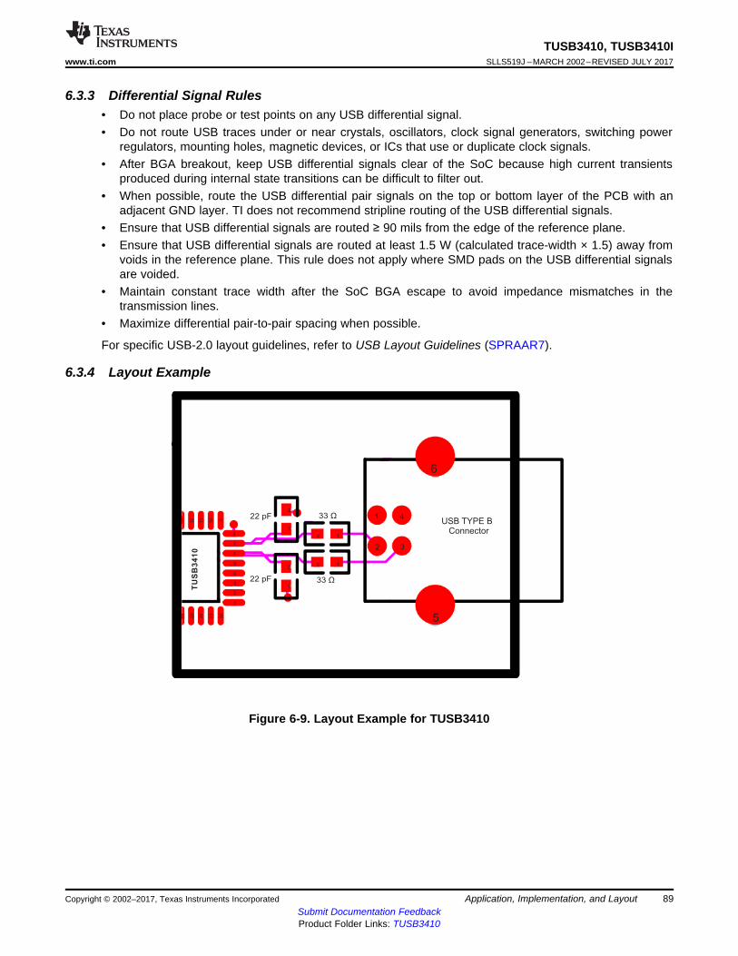
TU
SB
34
10
12
11
10 9
8
7
6
5
4
3
2
1
32
28
13
2
1
1
22
2 1
1
22 pF
22 pF 33 Ω
33 Ω
6
5
1 4
2 3
USB TYPE BConnector
31
30
29
89
TUSB3410, TUSB3410Iwww.ti.com SLLS519J –MARCH 2002–REVISED JULY 2017
Submit Documentation FeedbackProduct Folder Links: TUSB3410
Application, Implementation, and LayoutCopyright © 2002–2017, Texas Instruments Incorporated
6.3.3 Differential Signal Rules• Do not place probe or test points on any USB differential signal.• Do not route USB traces under or near crystals, oscillators, clock signal generators, switching power
regulators, mounting holes, magnetic devices, or ICs that use or duplicate clock signals.• After BGA breakout, keep USB differential signals clear of the SoC because high current transients
produced during internal state transitions can be difficult to filter out.• When possible, route the USB differential pair signals on the top or bottom layer of the PCB with an
adjacent GND layer. TI does not recommend stripline routing of the USB differential signals.• Ensure that USB differential signals are routed ≥ 90 mils from the edge of the reference plane.• Ensure that USB differential signals are routed at least 1.5 W (calculated trace-width × 1.5) away from
voids in the reference plane. This rule does not apply where SMD pads on the USB differential signalsare voided.
• Maintain constant trace width after the SoC BGA escape to avoid impedance mismatches in thetransmission lines.
• Maximize differential pair-to-pair spacing when possible.
For specific USB-2.0 layout guidelines, refer to USB Layout Guidelines (SPRAAR7).
6.3.4 Layout Example
Figure 6-9. Layout Example for TUSB3410
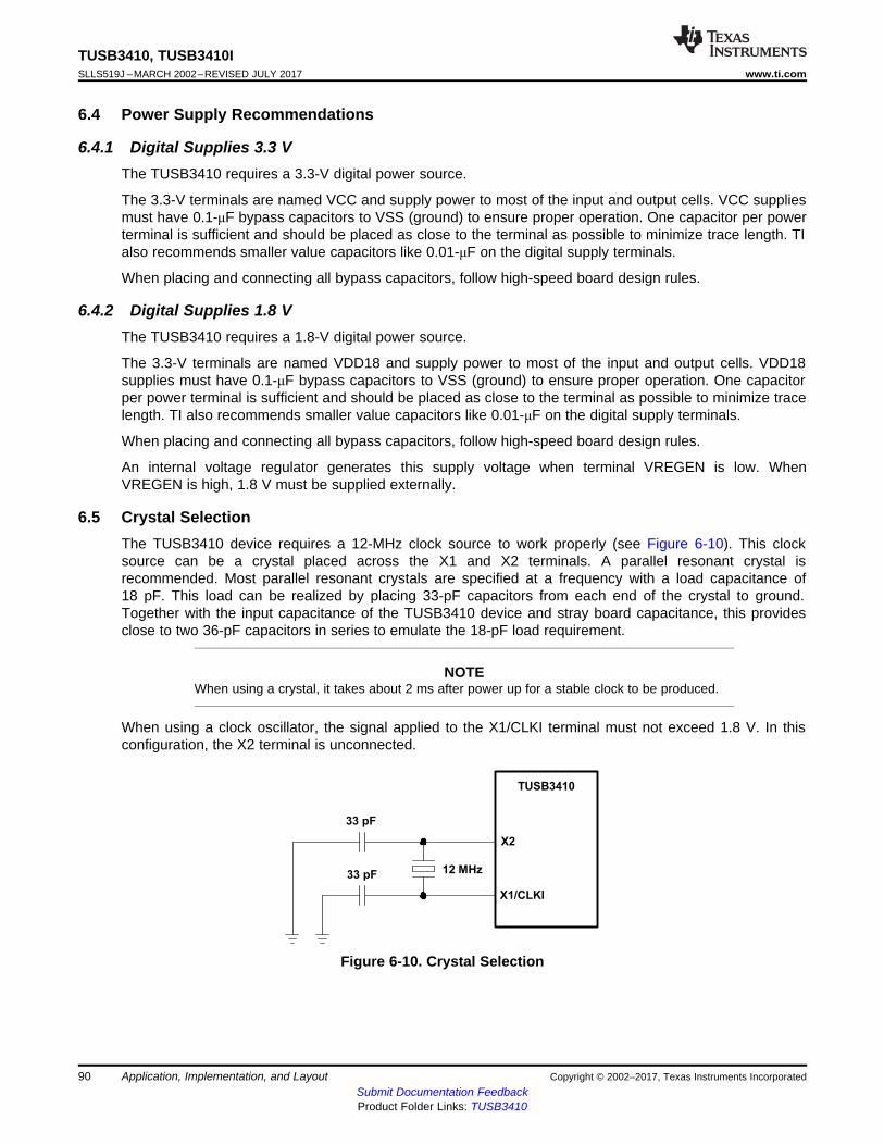
TUSB3410
33 pF
X2
33 pF 12 MHz
X1/CLKI
90
TUSB3410, TUSB3410ISLLS519J –MARCH 2002–REVISED JULY 2017 www.ti.com
Submit Documentation FeedbackProduct Folder Links: TUSB3410
Application, Implementation, and Layout Copyright © 2002–2017, Texas Instruments Incorporated
6.4 Power Supply Recommendations
6.4.1 Digital Supplies 3.3 VThe TUSB3410 requires a 3.3-V digital power source.
The 3.3-V terminals are named VCC and supply power to most of the input and output cells. VCC suppliesmust have 0.1-μF bypass capacitors to VSS (ground) to ensure proper operation. One capacitor per powerterminal is sufficient and should be placed as close to the terminal as possible to minimize trace length. TIalso recommends smaller value capacitors like 0.01-μF on the digital supply terminals.
When placing and connecting all bypass capacitors, follow high-speed board design rules.
6.4.2 Digital Supplies 1.8 VThe TUSB3410 requires a 1.8-V digital power source.
The 3.3-V terminals are named VDD18 and supply power to most of the input and output cells. VDD18supplies must have 0.1-μF bypass capacitors to VSS (ground) to ensure proper operation. One capacitorper power terminal is sufficient and should be placed as close to the terminal as possible to minimize tracelength. TI also recommends smaller value capacitors like 0.01-μF on the digital supply terminals.
When placing and connecting all bypass capacitors, follow high-speed board design rules.
An internal voltage regulator generates this supply voltage when terminal VREGEN is low. WhenVREGEN is high, 1.8 V must be supplied externally.
6.5 Crystal SelectionThe TUSB3410 device requires a 12-MHz clock source to work properly (see Figure 6-10). This clocksource can be a crystal placed across the X1 and X2 terminals. A parallel resonant crystal isrecommended. Most parallel resonant crystals are specified at a frequency with a load capacitance of18 pF. This load can be realized by placing 33-pF capacitors from each end of the crystal to ground.Together with the input capacitance of the TUSB3410 device and stray board capacitance, this providesclose to two 36-pF capacitors in series to emulate the 18-pF load requirement.
NOTEWhen using a crystal, it takes about 2 ms after power up for a stable clock to be produced.
When using a clock oscillator, the signal applied to the X1/CLKI terminal must not exceed 1.8 V. In thisconfiguration, the X2 terminal is unconnected.
Figure 6-10. Crystal Selection
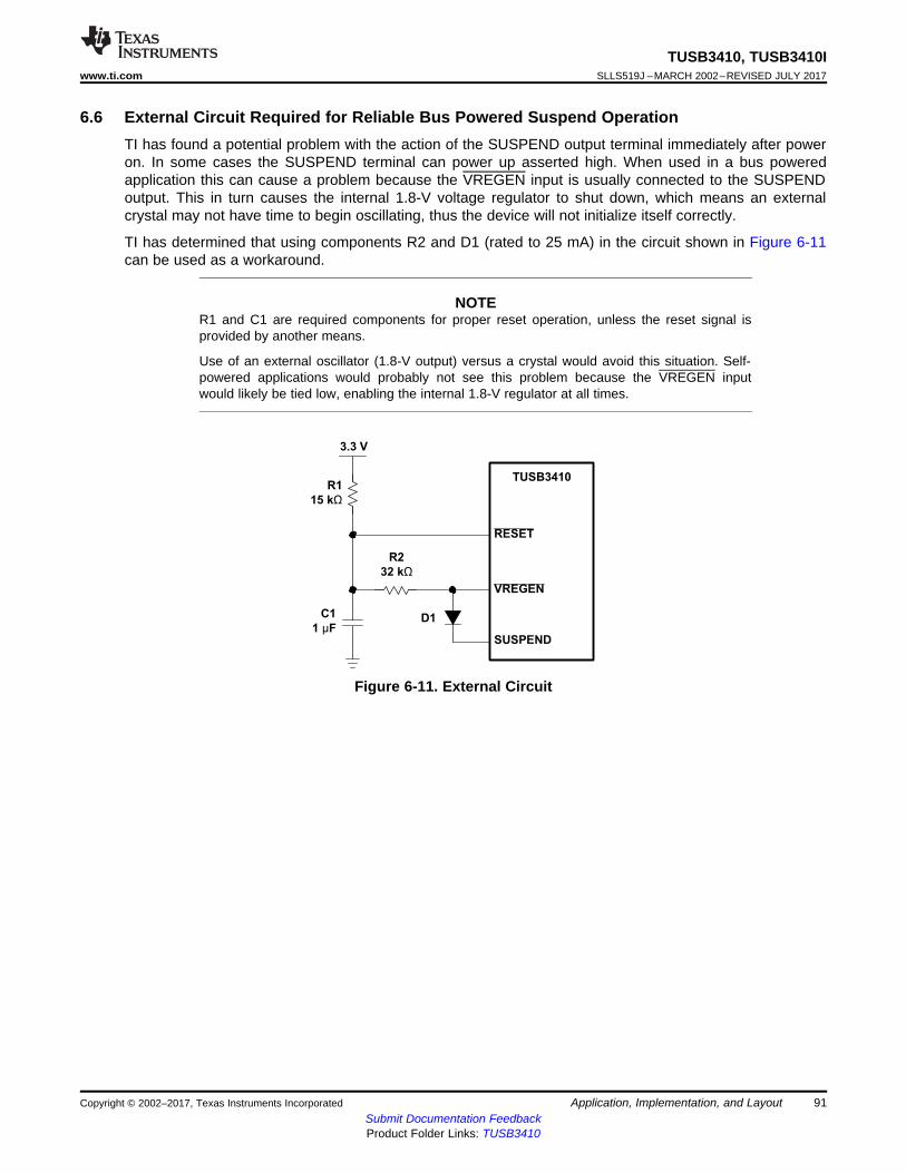
3.3 V
R1
15 kΩ
TUSB3410
C1
1 Fμ
R2
32 kΩ
D1
RESET
VREGEN
SUSPEND
91
TUSB3410, TUSB3410Iwww.ti.com SLLS519J –MARCH 2002–REVISED JULY 2017
Submit Documentation FeedbackProduct Folder Links: TUSB3410
Application, Implementation, and LayoutCopyright © 2002–2017, Texas Instruments Incorporated
6.6 External Circuit Required for Reliable Bus Powered Suspend OperationTI has found a potential problem with the action of the SUSPEND output terminal immediately after poweron. In some cases the SUSPEND terminal can power up asserted high. When used in a bus poweredapplication this can cause a problem because the VREGEN input is usually connected to the SUSPENDoutput. This in turn causes the internal 1.8-V voltage regulator to shut down, which means an externalcrystal may not have time to begin oscillating, thus the device will not initialize itself correctly.
TI has determined that using components R2 and D1 (rated to 25 mA) in the circuit shown in Figure 6-11can be used as a workaround.
NOTER1 and C1 are required components for proper reset operation, unless the reset signal isprovided by another means.
Use of an external oscillator (1.8-V output) versus a crystal would avoid this situation. Self-powered applications would probably not see this problem because the VREGEN inputwould likely be tied low, enabling the internal 1.8-V regulator at all times.
Figure 6-11. External Circuit
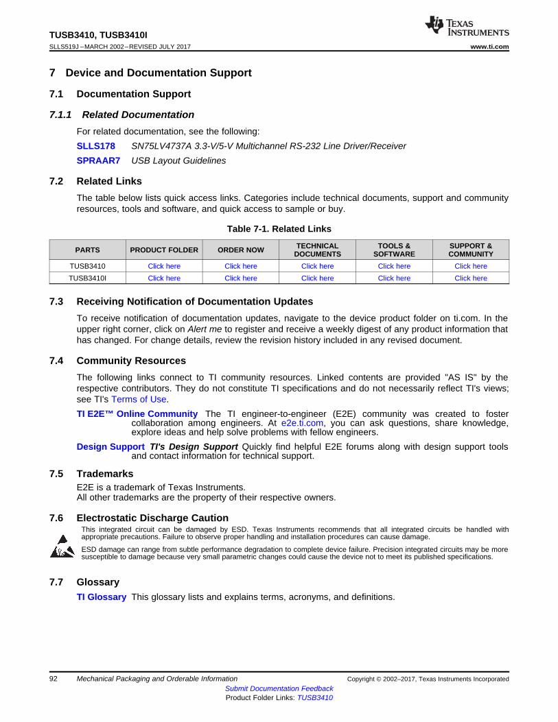
92
TUSB3410, TUSB3410ISLLS519J –MARCH 2002–REVISED JULY 2017 www.ti.com
Submit Documentation FeedbackProduct Folder Links: TUSB3410
Mechanical Packaging and Orderable Information Copyright © 2002–2017, Texas Instruments Incorporated
7 Device and Documentation Support
7.1 Documentation Support
7.1.1 Related DocumentationFor related documentation, see the following:SLLS178 SN75LV4737A 3.3-V/5-V Multichannel RS-232 Line Driver/ReceiverSPRAAR7 USB Layout Guidelines
7.2 Related LinksThe table below lists quick access links. Categories include technical documents, support and communityresources, tools and software, and quick access to sample or buy.
Table 7-1. Related Links
PARTS PRODUCT FOLDER ORDER NOW TECHNICALDOCUMENTS
TOOLS &SOFTWARE
SUPPORT &COMMUNITY
TUSB3410 Click here Click here Click here Click here Click hereTUSB3410I Click here Click here Click here Click here Click here
7.3 Receiving Notification of Documentation UpdatesTo receive notification of documentation updates, navigate to the device product folder on ti.com. In theupper right corner, click on Alert me to register and receive a weekly digest of any product information thathas changed. For change details, review the revision history included in any revised document.
7.4 Community ResourcesThe following links connect to TI community resources. Linked contents are provided "AS IS" by therespective contributors. They do not constitute TI specifications and do not necessarily reflect TI's views;see TI's Terms of Use.TI E2E™ Online Community The TI engineer-to-engineer (E2E) community was created to foster
collaboration among engineers. At e2e.ti.com, you can ask questions, share knowledge,explore ideas and help solve problems with fellow engineers.
Design Support TI's Design Support Quickly find helpful E2E forums along with design support toolsand contact information for technical support.
7.5 TrademarksE2E is a trademark of Texas Instruments.All other trademarks are the property of their respective owners.
7.6 Electrostatic Discharge CautionThis integrated circuit can be damaged by ESD. Texas Instruments recommends that all integrated circuits be handled withappropriate precautions. Failure to observe proper handling and installation procedures can cause damage.
ESD damage can range from subtle performance degradation to complete device failure. Precision integrated circuits may be moresusceptible to damage because very small parametric changes could cause the device not to meet its published specifications.
7.7 GlossaryTI Glossary This glossary lists and explains terms, acronyms, and definitions.
93
TUSB3410, TUSB3410Iwww.ti.com SLLS519J –MARCH 2002–REVISED JULY 2017
Submit Documentation FeedbackProduct Folder Links: TUSB3410
Mechanical Packaging and Orderable InformationCopyright © 2002–2017, Texas Instruments Incorporated
8 Mechanical Packaging and Orderable Information
8.1 Packaging InformationThe following pages include mechanical packaging and orderable information. This information is the mostcurrent data available for the designated devices. This data is subject to change without notice andrevision of this document. For browser-based versions of this data sheet, refer to the left-hand navigation.

PACKAGE OPTION ADDENDUM
www.ti.com 10-Dec-2020
Addendum-Page 1
PACKAGING INFORMATION
Orderable Device Status(1)
Package Type PackageDrawing
Pins PackageQty
Eco Plan(2)
Lead finish/Ball material
(6)
MSL Peak Temp(3)
Op Temp (°C) Device Marking(4/5)
Samples
TUSB3410IRHB ACTIVE VQFN RHB 32 73 RoHS & Green NIPDAU Level-2-260C-1 YEAR -40 to 85 3410I
TUSB3410IRHBR ACTIVE VQFN RHB 32 3000 RoHS & Green NIPDAU Level-2-260C-1 YEAR -40 to 85 3410I
TUSB3410IRHBT ACTIVE VQFN RHB 32 250 RoHS & Green NIPDAU Level-2-260C-1 YEAR -40 to 85 3410I
TUSB3410IVF ACTIVE LQFP VF 32 250 RoHS & Green NIPDAU Level-3-260C-168 HR -40 to 85 TUSB3410I
TUSB3410IVFG4 ACTIVE LQFP VF 32 250 RoHS & Green NIPDAU Level-3-260C-168 HR -40 to 85 TUSB3410I
TUSB3410RHB ACTIVE VQFN RHB 32 73 RoHS & Green NIPDAU Level-2-260C-1 YEAR 0 to 70 3410
TUSB3410RHBG4 ACTIVE VQFN RHB 32 73 RoHS & Green NIPDAU Level-2-260C-1 YEAR 0 to 70 3410
TUSB3410RHBR ACTIVE VQFN RHB 32 3000 RoHS & Green NIPDAU Level-2-260C-1 YEAR 0 to 70 3410
TUSB3410RHBT ACTIVE VQFN RHB 32 250 RoHS & Green NIPDAU Level-2-260C-1 YEAR 0 to 70 3410
TUSB3410VF ACTIVE LQFP VF 32 250 RoHS & Green NIPDAU Level-3-260C-168 HR 0 to 70 TUSB3410
TUSB3410VFG4 ACTIVE LQFP VF 32 250 RoHS & Green NIPDAU Level-3-260C-168 HR 0 to 70 TUSB3410
(1) The marketing status values are defined as follows:ACTIVE: Product device recommended for new designs.LIFEBUY: TI has announced that the device will be discontinued, and a lifetime-buy period is in effect.NRND: Not recommended for new designs. Device is in production to support existing customers, but TI does not recommend using this part in a new design.PREVIEW: Device has been announced but is not in production. Samples may or may not be available.OBSOLETE: TI has discontinued the production of the device.
(2) RoHS: TI defines "RoHS" to mean semiconductor products that are compliant with the current EU RoHS requirements for all 10 RoHS substances, including the requirement that RoHS substancedo not exceed 0.1% by weight in homogeneous materials. Where designed to be soldered at high temperatures, "RoHS" products are suitable for use in specified lead-free processes. TI mayreference these types of products as "Pb-Free".RoHS Exempt: TI defines "RoHS Exempt" to mean products that contain lead but are compliant with EU RoHS pursuant to a specific EU RoHS exemption.Green: TI defines "Green" to mean the content of Chlorine (Cl) and Bromine (Br) based flame retardants meet JS709B low halogen requirements of <=1000ppm threshold. Antimony trioxide basedflame retardants must also meet the <=1000ppm threshold requirement.
(3) MSL, Peak Temp. - The Moisture Sensitivity Level rating according to the JEDEC industry standard classifications, and peak solder temperature.
PACKAGE OPTION ADDENDUM
www.ti.com 10-Dec-2020
Addendum-Page 2
(4) There may be additional marking, which relates to the logo, the lot trace code information, or the environmental category on the device.
(5) Multiple Device Markings will be inside parentheses. Only one Device Marking contained in parentheses and separated by a "~" will appear on a device. If a line is indented then it is a continuationof the previous line and the two combined represent the entire Device Marking for that device.
(6) Lead finish/Ball material - Orderable Devices may have multiple material finish options. Finish options are separated by a vertical ruled line. Lead finish/Ball material values may wrap to twolines if the finish value exceeds the maximum column width.
Important Information and Disclaimer:The information provided on this page represents TI's knowledge and belief as of the date that it is provided. TI bases its knowledge and belief on informationprovided by third parties, and makes no representation or warranty as to the accuracy of such information. Efforts are underway to better integrate information from third parties. TI has taken andcontinues to take reasonable steps to provide representative and accurate information but may not have conducted destructive testing or chemical analysis on incoming materials and chemicals.TI and TI suppliers consider certain information to be proprietary, and thus CAS numbers and other limited information may not be available for release.
In no event shall TI's liability arising out of such information exceed the total purchase price of the TI part(s) at issue in this document sold by TI to Customer on an annual basis.
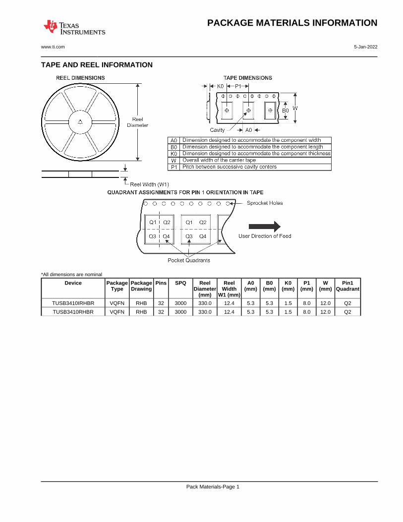
TAPE AND REEL INFORMATION
*All dimensions are nominal
Device PackageType
PackageDrawing
Pins SPQ ReelDiameter
(mm)
ReelWidth
W1 (mm)
A0(mm)
B0(mm)
K0(mm)
P1(mm)
W(mm)
Pin1Quadrant
TUSB3410IRHBR VQFN RHB 32 3000 330.0 12.4 5.3 5.3 1.5 8.0 12.0 Q2
TUSB3410RHBR VQFN RHB 32 3000 330.0 12.4 5.3 5.3 1.5 8.0 12.0 Q2
PACKAGE MATERIALS INFORMATION
www.ti.com 5-Jan-2022
Pack Materials-Page 1
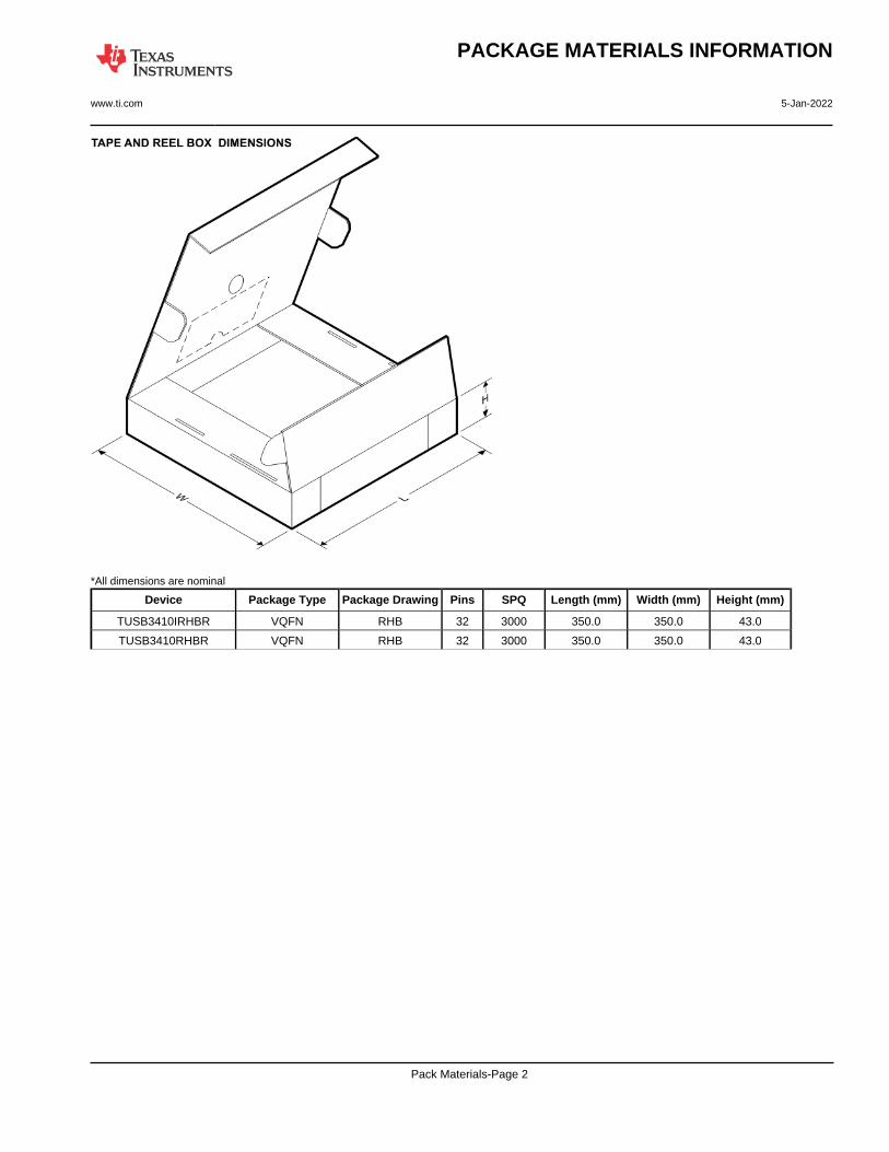
*All dimensions are nominal
Device Package Type Package Drawing Pins SPQ Length (mm) Width (mm) Height (mm)
TUSB3410IRHBR VQFN RHB 32 3000 350.0 350.0 43.0
TUSB3410RHBR VQFN RHB 32 3000 350.0 350.0 43.0
PACKAGE MATERIALS INFORMATION
www.ti.com 5-Jan-2022
Pack Materials-Page 2

TUBE
*All dimensions are nominal
Device Package Name Package Type Pins SPQ L (mm) W (mm) T (µm) B (mm)
TUSB3410IRHB RHB VQFN 32 73 381 6.73 2286 0
TUSB3410RHB RHB VQFN 32 73 381 6.73 2286 0
TUSB3410RHBG4 RHB VQFN 32 73 381 6.73 2286 0
PACKAGE MATERIALS INFORMATION
www.ti.com 5-Jan-2022
Pack Materials-Page 3

TRAY
Chamfer on Tray corner indicates Pin 1 orientation of packed units.
*All dimensions are nominal
Device PackageName
PackageType
Pins SPQ Unit arraymatrix
Maxtemperature
(°C)
L (mm) W(mm)
K0(µm)
P1(mm)
CL(mm)
CW(mm)
TUSB3410IVF VF LQFP 32 250 10 x 25 150 315 135.9 7620 12.2 11.1 11.25
TUSB3410IVFG4 VF LQFP 32 250 10 x 25 150 315 135.9 7620 12.2 11.1 11.25
TUSB3410VF VF LQFP 32 250 10 x 25 150 315 135.9 7620 12.2 11.1 11.25
TUSB3410VFG4 VF LQFP 32 250 10 x 25 150 315 135.9 7620 12.2 11.1 11.25
PACKAGE MATERIALS INFORMATION
www.ti.com 5-Jan-2022
Pack Materials-Page 4
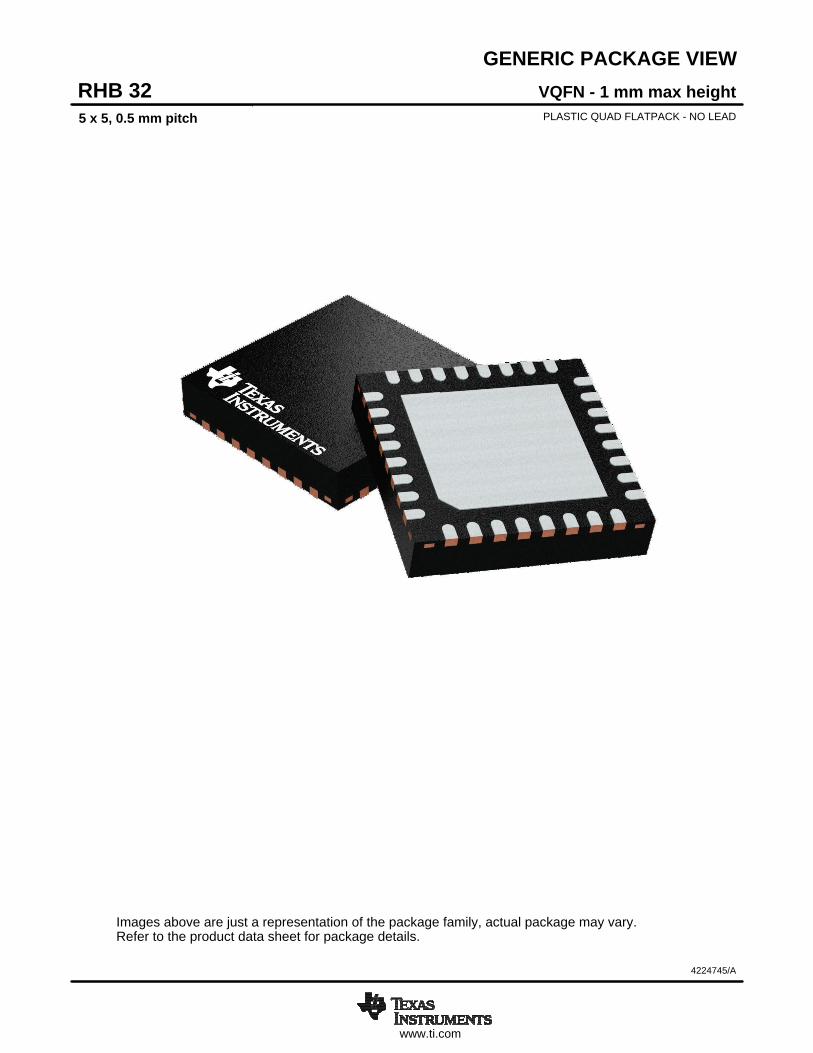
www.ti.com
GENERIC PACKAGE VIEW
Images above are just a representation of the package family, actual package may vary.Refer to the product data sheet for package details.
VQFN - 1 mm max heightRHB 32PLASTIC QUAD FLATPACK - NO LEAD5 x 5, 0.5 mm pitch
4224745/A
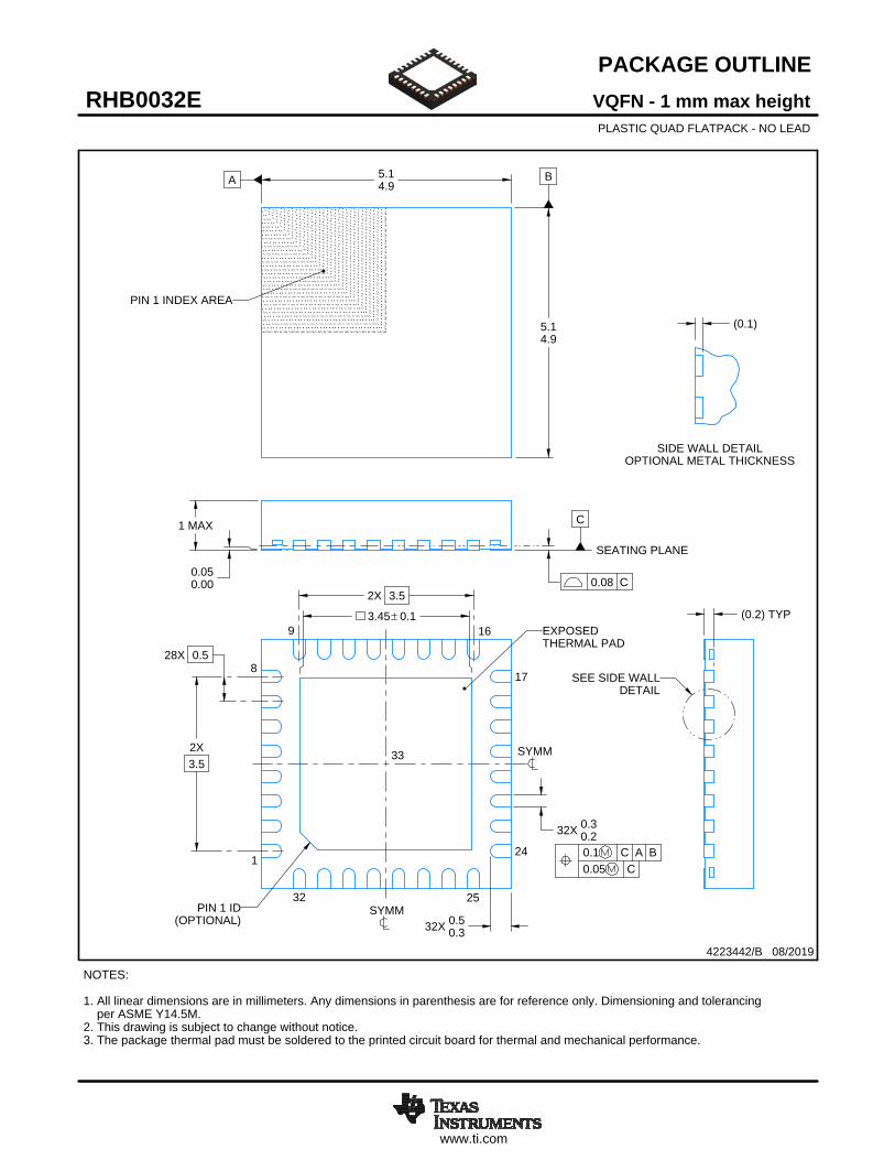
www.ti.com
PACKAGE OUTLINE
C
32X 0.30.2
3.45 0.1
32X 0.50.3
1 MAX
(0.2) TYP
0.050.00
28X 0.5
2X3.5
2X 3.5
A 5.14.9
B
5.14.9
(0.1)
VQFN - 1 mm max heightRHB0032EPLASTIC QUAD FLATPACK - NO LEAD
4223442/B 08/2019
PIN 1 INDEX AREA
0.08 C
SEATING PLANE
1
817
24
9 16
32 25
(OPTIONAL)PIN 1 ID
0.1 C A B0.05 C
EXPOSEDTHERMAL PAD
33 SYMM
SYMM
NOTES: 1. All linear dimensions are in millimeters. Any dimensions in parenthesis are for reference only. Dimensioning and tolerancing per ASME Y14.5M. 2. This drawing is subject to change without notice. 3. The package thermal pad must be soldered to the printed circuit board for thermal and mechanical performance.
SCALE 3.000
SEE SIDE WALLDETAIL
20.000
SIDE WALL DETAILOPTIONAL METAL THICKNESS
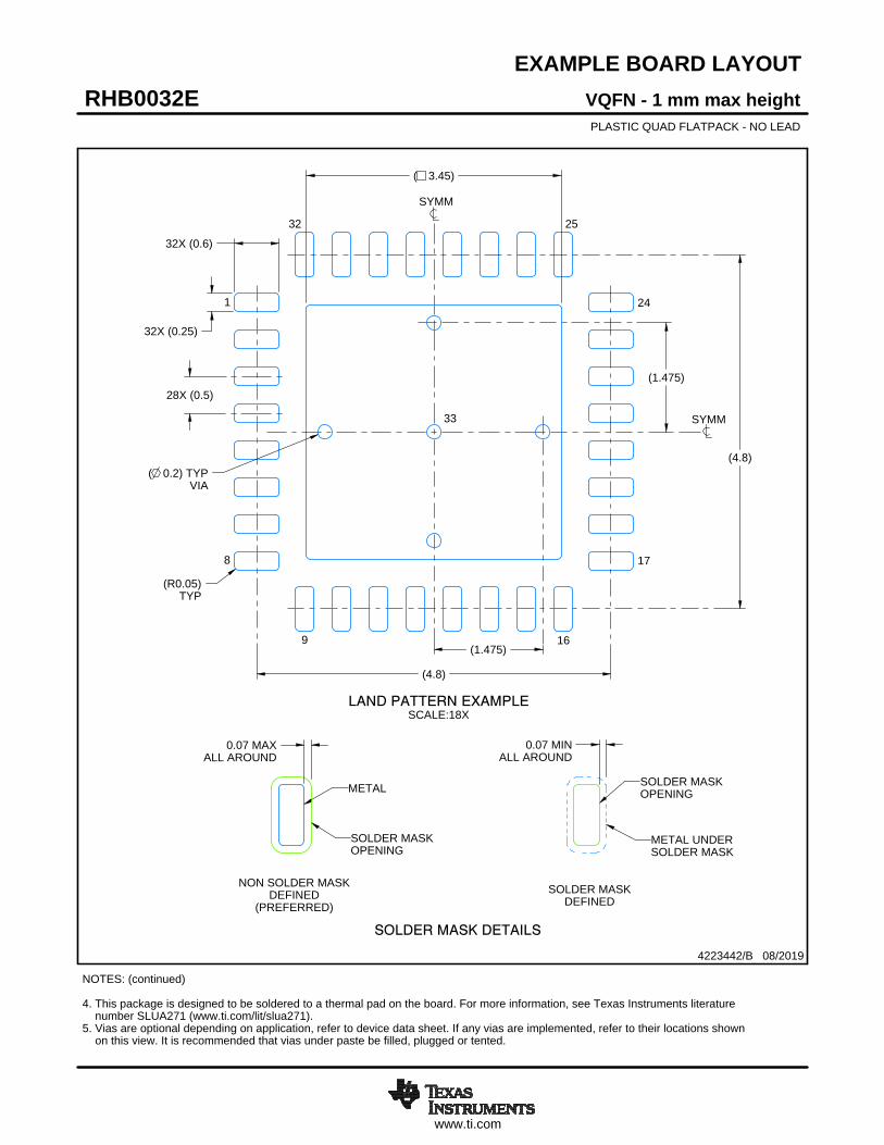
www.ti.com
EXAMPLE BOARD LAYOUT
(1.475)
0.07 MINALL AROUND
0.07 MAXALL AROUND
32X (0.25)
32X (0.6)
( 0.2) TYPVIA
28X (0.5)
(4.8)
(4.8)
(1.475)
( 3.45)
(R0.05)TYP
VQFN - 1 mm max heightRHB0032EPLASTIC QUAD FLATPACK - NO LEAD
4223442/B 08/2019
SYMM
1
8
9 16
17
24
2532
SYMM
LAND PATTERN EXAMPLESCALE:18X
NOTES: (continued) 4. This package is designed to be soldered to a thermal pad on the board. For more information, see Texas Instruments literature number SLUA271 (www.ti.com/lit/slua271).5. Vias are optional depending on application, refer to device data sheet. If any vias are implemented, refer to their locations shown on this view. It is recommended that vias under paste be filled, plugged or tented.
33
SOLDER MASKOPENING
METAL UNDERSOLDER MASK
SOLDER MASKDEFINED
METAL
SOLDER MASKOPENING
SOLDER MASK DETAILS
NON SOLDER MASKDEFINED
(PREFERRED)
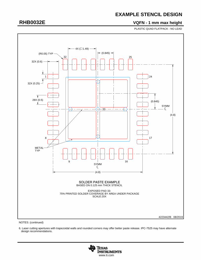
www.ti.com
EXAMPLE STENCIL DESIGN
32X (0.6)
32X (0.25)
28X (0.5)
(4.8)
(4.8)
4X ( 1.49)
(0.845)
(0.845)(R0.05) TYP
VQFN - 1 mm max heightRHB0032EPLASTIC QUAD FLATPACK - NO LEAD
4223442/B 08/2019
NOTES: (continued) 6. Laser cutting apertures with trapezoidal walls and rounded corners may offer better paste release. IPC-7525 may have alternate design recommendations.
33
SYMM
METALTYP
SOLDER PASTE EXAMPLEBASED ON 0.125 mm THICK STENCIL
EXPOSED PAD 33:
75% PRINTED SOLDER COVERAGE BY AREA UNDER PACKAGESCALE:20X
SYMM
1
8
9 16
17
24
2532
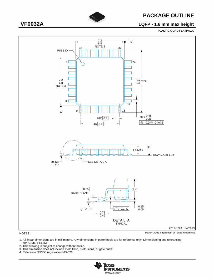
www.ti.com
PACKAGE OUTLINE
C
32X 0.450.2528X 0.8
PIN 1 ID
(0.13)TYP
0.150.050 -7
4X 5.6
9.28.8 TYP
0.750.45
B7.26.8
NOTE 3
A
7.26.8
NOTE 3
0.25GAGE PLANE
1.6 MAX
(1.4)
PLASTIC QUAD FLATPACK
LQFP - 1.6 mm max heightVF0032APLASTIC QUAD FLATPACK
4219769/A 04/2019
NOTES: 1. All linear dimensions are in millimeters. Any dimensions in parenthesis are for reference only. Dimensioning and tolerancing per ASME Y14.5M. 2. This drawing is subject to change without notice.3. This dimension does not include mold flash, protrusions, or gate burrs.4. Reference JEDEC registration MS-026.
PowerPAD is a trademark of Texas Instruments.
1
8
9 16
17
24
2532
0.2 C A B
SEE DETAIL A
SEATING PLANE
A 15DETAIL ATYPICAL
0.1 C
SCALE 1.700
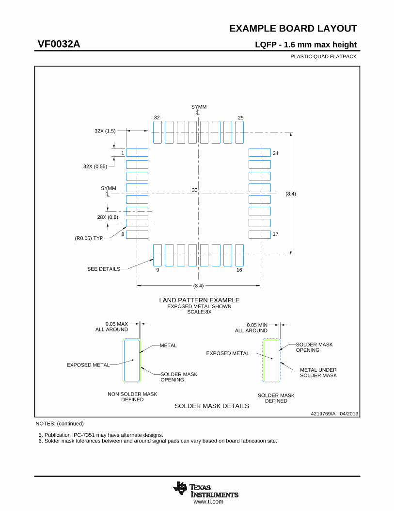
www.ti.com
EXAMPLE BOARD LAYOUT
0.05 MAXALL AROUND
0.05 MINALL AROUND
(8.4)
(8.4)
28X (0.8)
32X (1.5)
32X (0.55)
(R0.05) TYP
LQFP - 1.6 mm max heightVF0032APLASTIC QUAD FLATPACK
4219769/A 04/2019
NOTES: (continued) 5. Publication IPC-7351 may have alternate designs. 6. Solder mask tolerances between and around signal pads can vary based on board fabrication site.
LAND PATTERN EXAMPLEEXPOSED METAL SHOWN
SCALE:8X
SYMM
SYMM
32 25
9 16
17
241
8
33
SEE DETAILS
METAL
SOLDER MASKOPENING
NON SOLDER MASKDEFINED
SOLDER MASK DETAILS
EXPOSED METAL
SOLDER MASKOPENING
METAL UNDERSOLDER MASK
SOLDER MASKDEFINED
EXPOSED METAL
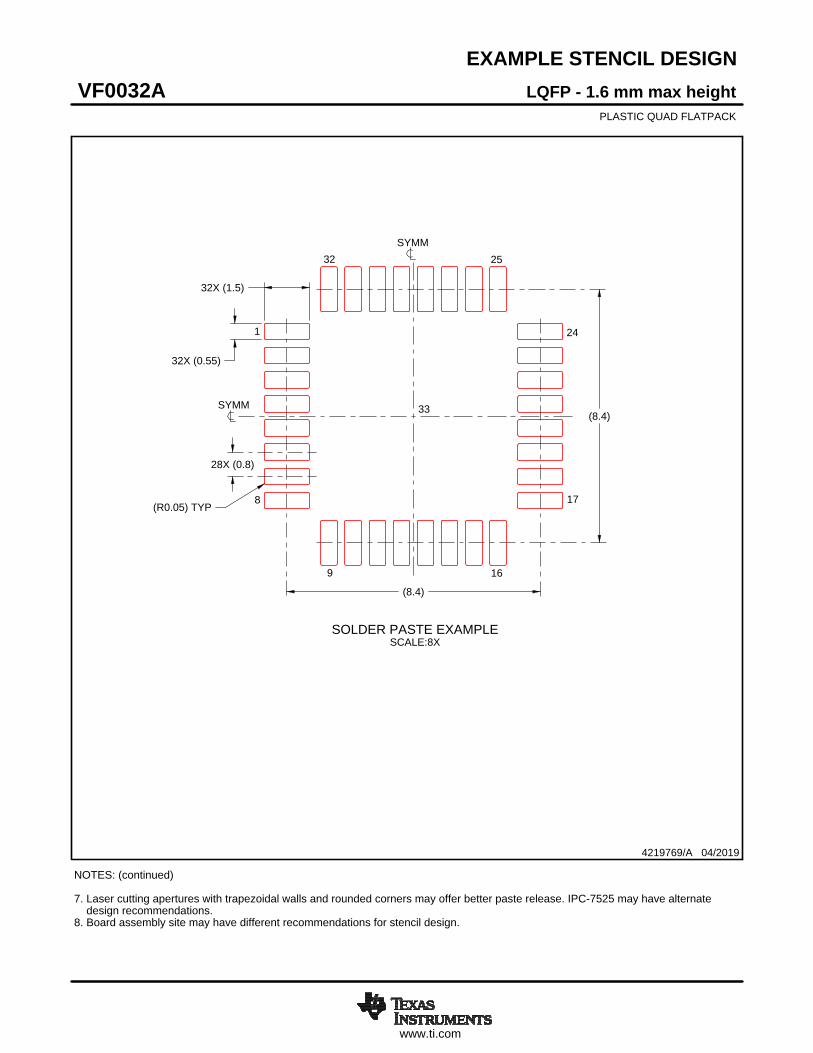
www.ti.com
EXAMPLE STENCIL DESIGN
28X (0.8)
32X (1.5)
32X (0.55)
(R0.05) TYP
(8.4)
(8.4)
LQFP - 1.6 mm max heightVF0032APLASTIC QUAD FLATPACK
4219769/A 04/2019
NOTES: (continued) 7. Laser cutting apertures with trapezoidal walls and rounded corners may offer better paste release. IPC-7525 may have alternate design recommendations. 8. Board assembly site may have different recommendations for stencil design.
SOLDER PASTE EXAMPLESCALE:8X
SYMM
SYMM
32 25
9 16
17
241
8
33
IMPORTANT NOTICE AND DISCLAIMERTI PROVIDES TECHNICAL AND RELIABILITY DATA (INCLUDING DATA SHEETS), DESIGN RESOURCES (INCLUDING REFERENCE DESIGNS), APPLICATION OR OTHER DESIGN ADVICE, WEB TOOLS, SAFETY INFORMATION, AND OTHER RESOURCES “AS IS” AND WITH ALL FAULTS, AND DISCLAIMS ALL WARRANTIES, EXPRESS AND IMPLIED, INCLUDING WITHOUT LIMITATION ANY IMPLIED WARRANTIES OF MERCHANTABILITY, FITNESS FOR A PARTICULAR PURPOSE OR NON-INFRINGEMENT OF THIRD PARTY INTELLECTUAL PROPERTY RIGHTS.These resources are intended for skilled developers designing with TI products. You are solely responsible for (1) selecting the appropriate TI products for your application, (2) designing, validating and testing your application, and (3) ensuring your application meets applicable standards, and any other safety, security, regulatory or other requirements.These resources are subject to change without notice. TI grants you permission to use these resources only for development of an application that uses the TI products described in the resource. Other reproduction and display of these resources is prohibited. No license is granted to any other TI intellectual property right or to any third party intellectual property right. TI disclaims responsibility for, and you will fully indemnify TI and its representatives against, any claims, damages, costs, losses, and liabilities arising out of your use of these resources.TI’s products are provided subject to TI’s Terms of Sale or other applicable terms available either on ti.com or provided in conjunction with such TI products. TI’s provision of these resources does not expand or otherwise alter TI’s applicable warranties or warranty disclaimers for TI products.TI objects to and rejects any additional or different terms you may have proposed. IMPORTANT NOTICE
Mailing Address: Texas Instruments, Post Office Box 655303, Dallas, Texas 75265Copyright © 2022, Texas Instruments Incorporated