hardware architecture overview bluegene/l design team ibm … · z“custom design” twist:...
TRANSCRIPT

10/17/2003 1
BlueGene/L
Hardware Architecture Overview
BlueGene/L design teamIBM Research
10/17/2003 2
BG/L Hardware Architecture - October 2003
Ruud Haring: BlueGene/L Compute Chip Overview
Dirk Hoenicke: BLC chip microarchitecture , networks & performance
Gerry Kopcsay: Power, Packaging, Cooling
10/17/2003 3
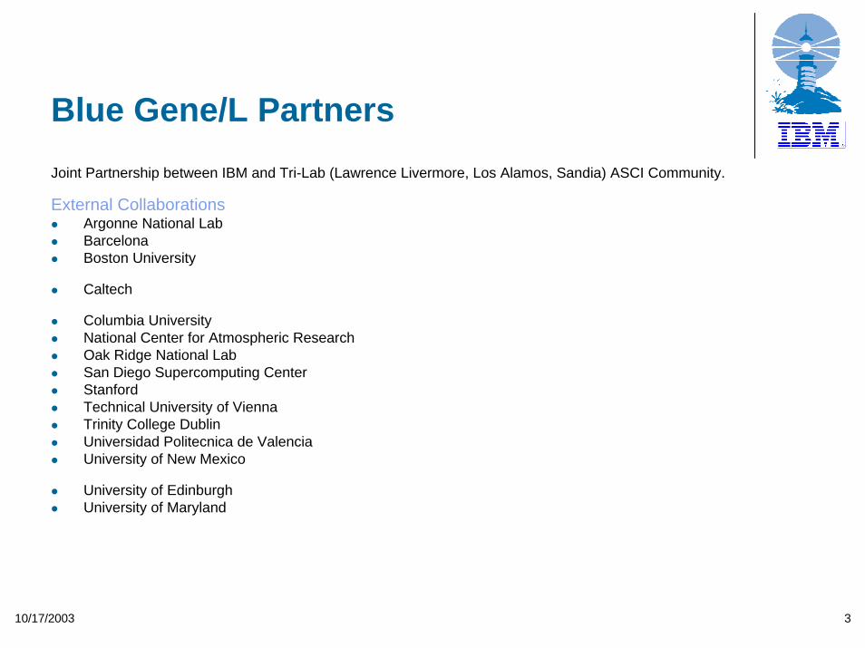
Blue Gene/L PartnersJoint Partnership between IBM and Tri-Lab (Lawrence Livermore, Los Alamos, Sandia) ASCI Community.
External CollaborationsArgonne National Lab BarcelonaBoston University
Caltech
Columbia University National Center for Atmospheric Research Oak Ridge National Lab San Diego Supercomputing CenterStanford Technical University of Vienna Trinity College Dublin Universidad Politecnica de Valencia University of New Mexico
University of Edinburgh University of Maryland

10/17/2003 4
What is BG/L
A 64k node highly integrated supercomputer based on system-on-a-chip technology.
Two ASICs: BlueGene/L Compute (BLC)
BlueGene/L Link (BLL)Focus is on numerically intensive scientific problems.180-360 TFlop peak performance.Strategic partnership with LLNL.
Validation and optimization of architecture based on real applications Accustomed to "new architectures" and will work hard to adapt to constraints.Assist us in the investigation of the reach of this machine
Grand challenge science stressI/O, memory (bandwidth, size and latency), and processing power.
10/17/2003 5
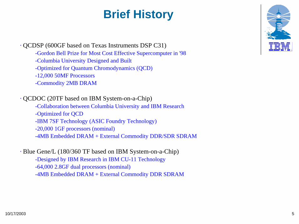
Brief History
· QCDSP (600GF based on Texas Instruments DSP C31)-Gordon Bell Prize for Most Cost Effective Supercomputer in '98-Columbia University Designed and Built -Optimized for Quantum Chromodynamics (QCD)-12,000 50MF Processors-Commodity 2MB DRAM
· QCDOC (20TF based on IBM System-on-a-Chip)-Collaboration between Columbia University and IBM Research-Optimized for QCD-IBM 7SF Technology (ASIC Foundry Technology)-20,000 1GF processors (nominal)-4MB Embedded DRAM + External Commodity DDR/SDR SDRAM
· Blue Gene/L (180/360 TF based on IBM System-on-a-Chip)-Designed by IBM Research in IBM CU-11 Technology-64,000 2.8GF dual processors (nominal)-4MB Embedded DRAM + External Commodity DDR SDRAM
10/17/2003 6
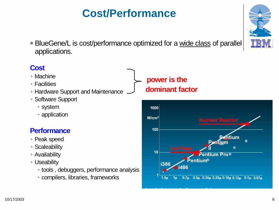
Cost/Performance
power is the
dominant factor
BlueGene/L is cost/performance optimized for a wide class of parallel applications.
CostMachineFacilitiesHardware Support and MaintenanceSoftware Support
systemapplication
PerformancePeak speed Scaleability Availability Useability
tools , debuggers, performance analysiscompilers, libraries, frameworks
10/17/2003 7
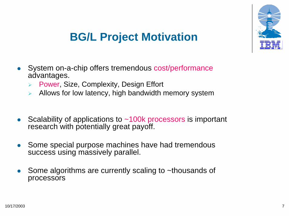
BG/L Project Motivation
System on-a-chip offers tremendous cost/performanceadvantages.
Power, Size, Complexity, Design EffortAllows for low latency, high bandwidth memory system
Scalability of applications to ~100k processors is important research with potentially great payoff.
Some special purpose machines have had tremendous success using massively parallel.
Some algorithms are currently scaling to ~thousands of processors
10/17/2003 8
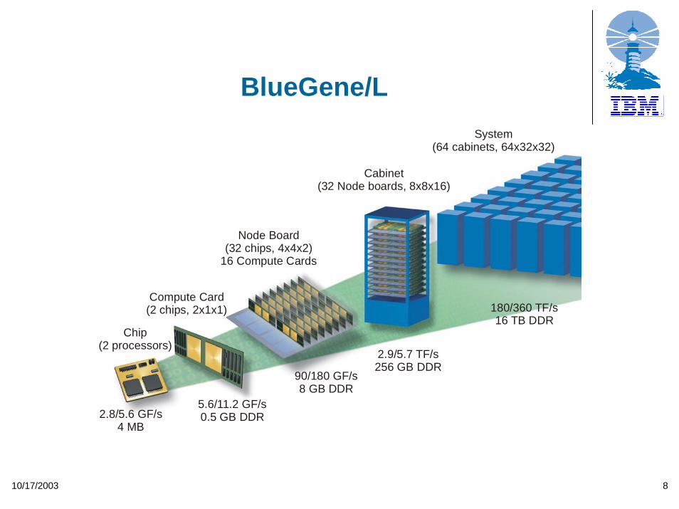
BlueGene/L
Chip(2 processors)
Compute Card(2 chips, 2x1x1)
Node Board(32 chips, 4x4x2)
16 Compute Cards
System(64 cabinets, 64x32x32)
Cabinet(32 Node boards, 8x8x16)
2.8/5.6 GF/s4 MB
5.6/11.2 GF/s0.5 GB DDR
90/180 GF/s8 GB DDR
2.9/5.7 TF/s256 GB DDR
180/360 TF/s16 TB DDR
10/17/2003 9
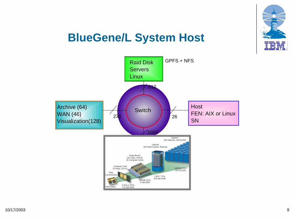
BlueGene/L System Host
Raid DiskServersLinux
Archive (64)WAN (46)Visualization(128)
SwitchHostFEN: AIX or LinuxSN
230 26
512
1024
GPFS + NFS
Chip(2 processors)
Compute Card(2 chips, 2x1x1)
Node Board(32 chips, 4x4x2)
16 Compute Cards
System(64 cabinets, 64x32x32)
Cabinet(32 Node boards, 8x8x16)
2.8/5.6 GF/s4 MB
5.6/11.2 GF/s0.5 GB DDR
90/180 GF/s8 GB DDR
2.9/5.7 TF/s256 GB DDR
180/360 TF/s16 TB DDR
10/17/2003 10
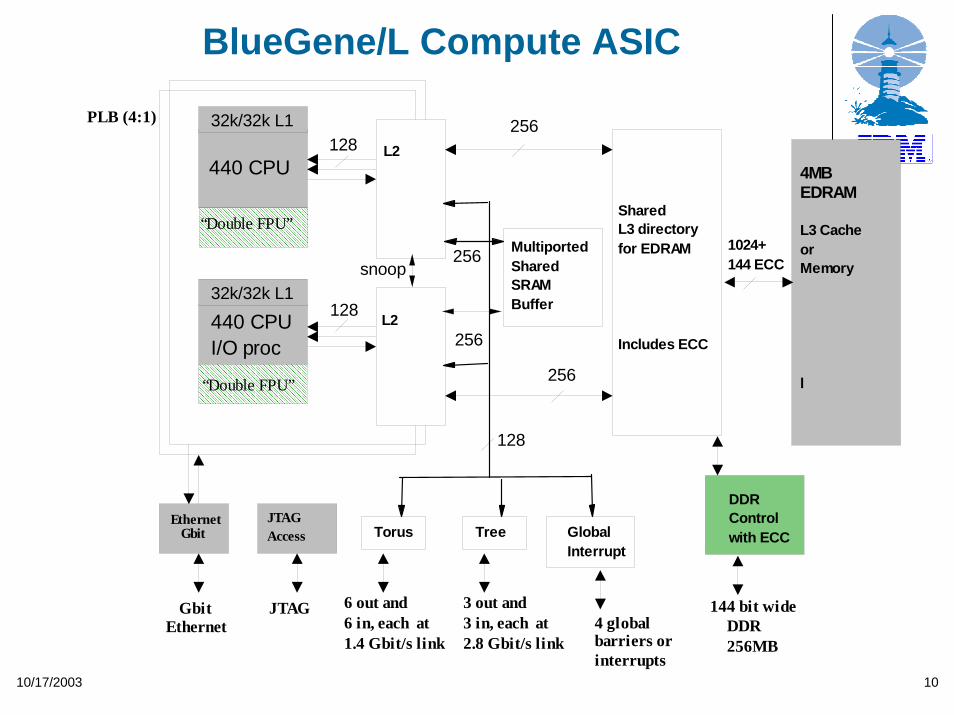
BlueGene/L Compute ASIC
PLB (4:1)
“Double FPU”
Ethernet Gbit
JTAGAccess
144 bit wide DDR256MB
JTAG
Gbit Ethernet
440 CPU
440 CPUI/O proc
L2
L2
MultiportedSharedSRAM Buffer
Torus
DDR Control with ECC
SharedL3 directoryfor EDRAM
Includes ECC
4MB EDRAM
L3 CacheorMemory
l
6 out and6 in, each at 1.4 Gbit/s link
256
256
1024+144 ECC256
128
128
32k/32k L1
32k/32k L1
“Double FPU”
256
snoop
Tree
3 out and3 in, each at 2.8 Gbit/s link
GlobalInterrupt
4 global barriers orinterrupts
128

10/17/2003 11
System designed for high reliability
BLC ASIC All SRAMs in are ECC protected -- except L1 caches in PPC440 and EthernetL1 caches in 440 cores are parity protected with multiple operating modesMost internal busses have parity detectioneDRAM is ECC protectedController for external DRAM supports memory scrub and ECC with nibble kill reliability. Bit sparing allows for swapping in spare nibble for further reliability.All error types can be counted and used for predictive failure analysis
Networks:24 packet CRC + 32 bit “static” CRCHardware retry for all CRC fails. – Never seen an escape through protocolOptional error injection allows for aggressive testing of link protocol coverageLinks are temperature and voltage compensating
Hardware support for fault isolationCan determine first node that generates a non-repeatable computation in a deterministic calculation
Redundancy in power, cooling and cabling
10/17/2003 12
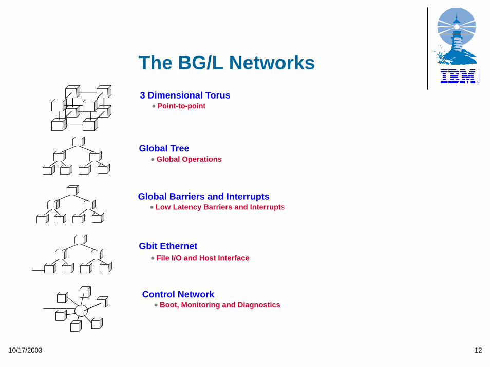
The BG/L Networks
Gbit EthernetFile I/O and Host Interface
3 Dimensional TorusPoint-to-point
Global TreeGlobal Operations
Global Barriers and Interrupts
Low Latency Barriers and Interrupts
Control Network Boot, Monitoring and Diagnostics
10/17/2003 13
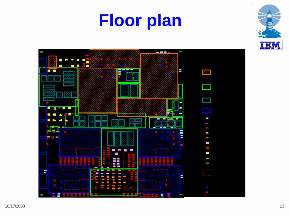
Floor plan

10/17/2003 14
System-on-a-Chip
IBM Cu-11 (0.13 mu technology) ASIC with:hard cores -- dual ( PPC440 + double FPU ), PLLsoft cores -- Ethernet /DMA sub-systemcustom I/O books for high speed signalingeDRAM (32 Mb/chip)SRAM (~2 Mb/chip), fuses, ECID
“Custom design” twist: bitstacksguided placement, auto wiringcritical for high speed send/capture of serialized Torus/Tree far exceeds "normal" ASIC speeds -- up to 1.4 GHz clock.Organizes wiring congestion at wide eDRAM ports
IBM E&TS (Rochester, MN) style PD and testcareful clock design -- about 90 clock signals; 30 clock sub-domainsJTAG-based co-processor for in-system test/bring-up
10/17/2003 15
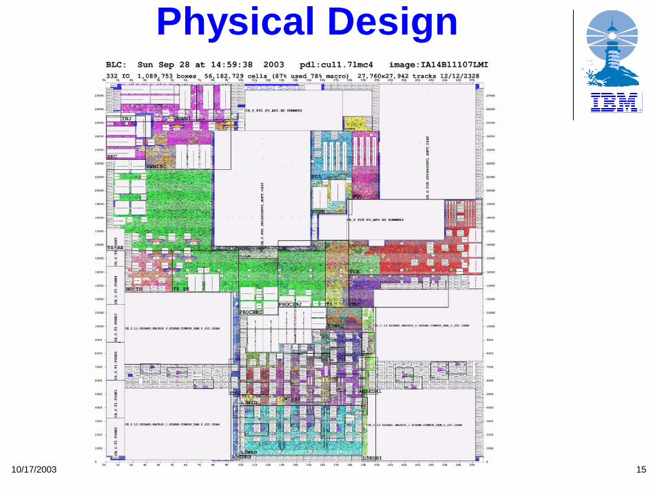
Physical Design

10/17/2003 16
Chip area usage
440+Hummer2
eDRAMsI/O cellsDecaps
Fuse/BIST
DTFILL
Soft Cores
SRAM+RA
Cust. LogicPercent of chip
440+Hummer2eDRAMsI/O cellsDecapsFuse/BISTDTFILLSoft CoresSRAM+RACust. Logic

10/17/2003 17
Prototype Bring-Up
BLC DD1.0 Power-On on 06/16/2003
Presently (10/10) > 600 chips running in various test stations1,2,8,32,128, 256, 512-waysrunning anything from low level tests to applications to benchmarksNo show stoppers found.
The hardware works! Pace of bring-up limited by s/w and resources.
Outlook is good to do DD2.0 RIT in November
BLC DD2.0 (production version):No major functional differenceBetter frequencyImprovements for robustness, diagnostics, error recovery.
10/17/2003 18
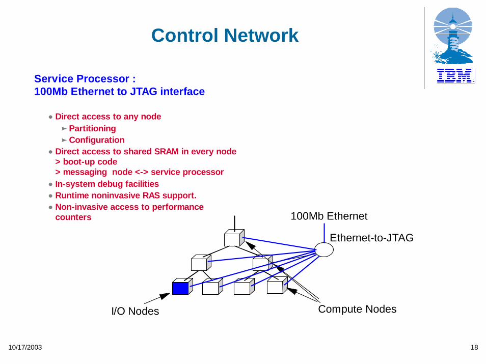
Control Network
Service Processor : 100Mb Ethernet to JTAG interface
Direct access to any nodePartitioningConfiguration
Direct access to shared SRAM in every node > boot-up code> messaging node <-> service processorIn-system debug facilitiesRuntime noninvasive RAS support.Non-invasive access to performance counters
Compute Nodes
100Mb Ethernet
Ethernet-to-JTAG
I/O Nodes
10/17/2003 19
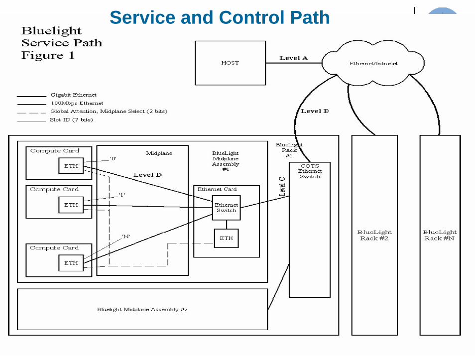
Service and Control Path

10/17/2003 20
Logic designArchitect Alan Gara Hummer2 Chuck Wait + teamL2 Dirk Hoenicke, Martin OhmachtL3, SRAM, Lockbox Martin OhmachtDDR controller Jim MarcellaTorus Dong Chen, Pavlos Vranas, Sarabjeet SinghTree Dirk Hoenicke, Matt BlumrichHigh Speed Serial Comm Alan Gara, Dong Chen, Sarabjeet SinghGlobal Interrupts Dong Chen, Alan GaraEMAC4/PLB/DCR/BIC Martin OhmachtPerformance Counters Dirk HoenickeClock Tree Matt EllavskyTest & Bring-up structures Marc Dombrowa, Ruud Haring,
Steve Douskey, Mike Hamilton, Jim MarcellaIOs Ruud HaringLogic integration Martin Ohmacht, Marc DombrowaLibraries Dan Beece
10/17/2003 21
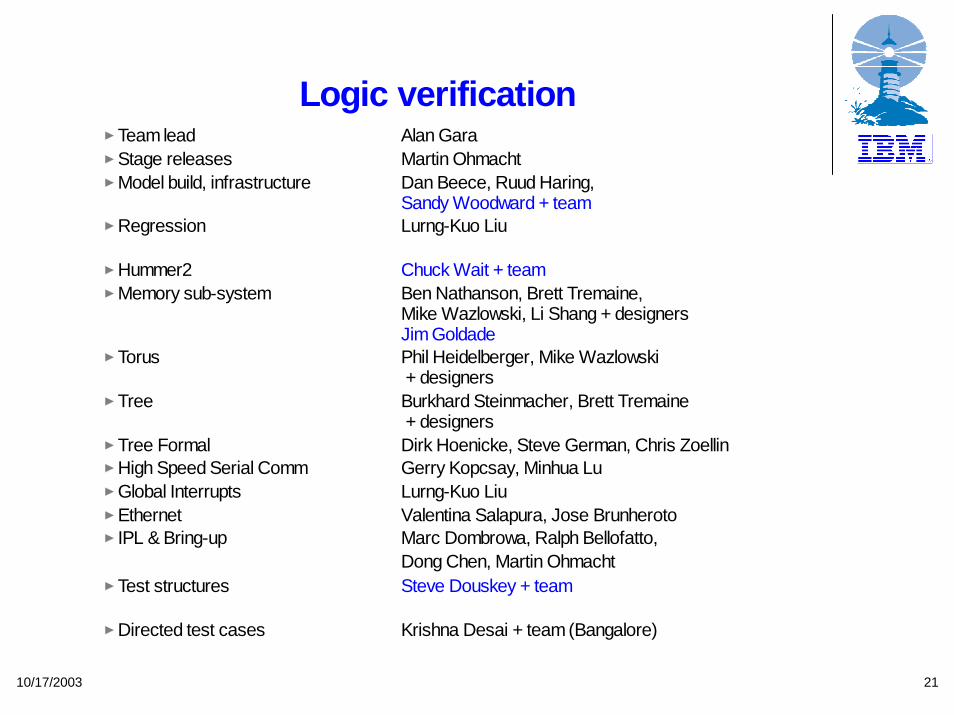
Logic verificationTeam lead Alan Gara Stage releases Martin OhmachtModel build, infrastructure Dan Beece, Ruud Haring,
Sandy Woodward + teamRegression Lurng-Kuo Liu
Hummer2 Chuck Wait + teamMemory sub-system Ben Nathanson, Brett Tremaine,
Mike Wazlowski, Li Shang + designersJim Goldade
Torus Phil Heidelberger, Mike Wazlowski + designers
Tree Burkhard Steinmacher, Brett Tremaine + designers
Tree Formal Dirk Hoenicke, Steve German, Chris ZoellinHigh Speed Serial Comm Gerry Kopcsay, Minhua LuGlobal Interrupts Lurng-Kuo LiuEthernet Valentina Salapura, Jose BrunherotoIPL & Bring-up Marc Dombrowa, Ralph Bellofatto,
Dong Chen, Martin OhmachtTest structures Steve Douskey + team
Directed test cases Krishna Desai + team (Bangalore)
10/17/2003 22
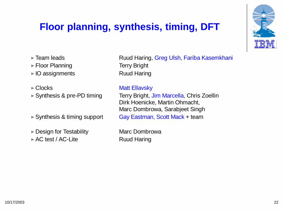
Floor planning, synthesis, timing, DFT
Team leads Ruud Haring, Greg Ulsh, Fariba KasemkhaniFloor Planning Terry BrightIO assignments Ruud Haring
Clocks Matt EllavskySynthesis & pre-PD timing Terry Bright, Jim Marcella, Chris Zoellin
Dirk Hoenicke, Martin Ohmacht, Marc Dombrowa, Sarabjeet Singh
Synthesis & timing support Gay Eastman, Scott Mack + team
Design for Testability Marc Dombrowa AC test / AC-Lite Ruud Haring
10/17/2003 23
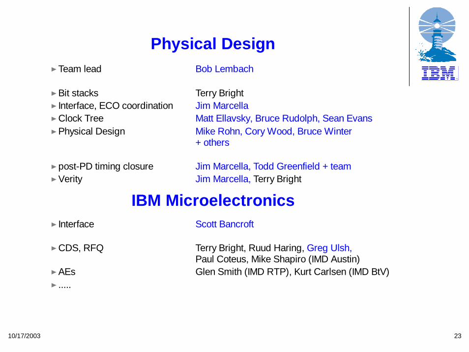
Physical DesignTeam lead Bob Lembach
Bit stacks Terry BrightInterface, ECO coordination Jim MarcellaClock Tree Matt Ellavsky, Bruce Rudolph, Sean EvansPhysical Design Mike Rohn, Cory Wood, Bruce Winter
+ others
post-PD timing closure Jim Marcella, Todd Greenfield + teamVerity Jim Marcella, Terry Bright
IBM MicroelectronicsInterface Scott Bancroft
CDS, RFQ Terry Bright, Ruud Haring, Greg Ulsh,Paul Coteus, Mike Shapiro (IMD Austin)
AEs Glen Smith (IMD RTP), Kurt Carlsen (IMD BtV).....