emulating ibm bluegene on a linux mpi...
TRANSCRIPT
EMULATING IBM BLUEGENE ON A LINUX
MPI CLUSTER
Karthik Ganesan and Vishwanath Venkatesan

Acknowledgement
We are very grateful to Professor N. Venkateswaran, affectionately known as Waran
by his students, who is the Mentor for this Project and also coined us towards achiev-
ing research goals at WAran Research FoundaTion (WARFT), where we associated
with him as part-time Research Trainees. Prof. Waran has always been motivating
us through his golden words of research. We express our sincere thanks and gratitude
to him. His perseverance and passion towards research have always fascinated us,
which we hope will take us to greater heights. His lectures and motivating words are
engraved in our hearts to take up research profession in the time to come.
We also express our sincere thanks to our Internal Guide, Ms S R Malathi,
Senior Lecturer for her guidance in the successful completion of this project.
It will not be out of place to mention here that Prof. T Srinivasan has put in
lot of efforts and extended maximum cooperation in installing a High Performance
Linux Cluster in Sri Venkateswara College of Engineering as a maiden attempt for
which he deserves kudos. We place on record our sincere thanks and gratitude for
this gesture.
We also thank Mr. S Sampath Raghavan, Mr. S Sathyaraj, and Mr. M
Tamil Selvan for their untiring help and assistance in successfully installing this
cluster for the first time in our college.
1
Abstract
The new and previous No. 1 is DOE’s IBM BlueGene/L system, in-
stalled at DOE’s Lawrence Livermore National Laboratory (LLNL). It
has doubled in size (again) and has now achieved a record Linpack per-
formance of 280.6 TFlop/s. It is still the only system ever to exceed
the 100 TFlop/s mark. This project is being carried out at WAran
Research FoundaTion as a part of WARFT’s major research initiative
into Brain Modeling and Supercomputing. The focus of this project
is to investigate deeper into the network and node characteristics of
BlueGene/L with regard to Performance and Power. To study these
aspects, we emulate the IBM BlueGene. This being a very complex
a computationally intensive process, a high Performance System like
a Linux MPI cluster is essential. Specific Benchmark applications like
LinPack benchmark will be run on the emulated BlueGene cluster.
Contents
1 Introduction 6
2 Overview of IBM Bluegene Supercomputer 9
2.1 Bluegene Node Overview . . . . . . . . . . . . . . . . . . . . . . . . . 14
2.2 Power PC Instruction Set Architecture . . . . . . . . . . . . . . . . . 23
2.3 Memory Architecture . . . . . . . . . . . . . . . . . . . . . . . . . . . 25
2.3.1 The PowerPc Core and L1 Cache . . . . . . . . . . . . . . . . 27
2.3.2 L2 Cache . . . . . . . . . . . . . . . . . . . . . . . . . . . . . 29
2.3.3 L3 Cache . . . . . . . . . . . . . . . . . . . . . . . . . . . . . 31
2.3.4 Lockbox and SRAM . . . . . . . . . . . . . . . . . . . . . . . 35
2.3.5 Performance of the Memory Subsystem . . . . . . . . . . . . . 36
2.4 Interconnection Network in Bluegene . . . . . . . . . . . . . . . . . . 41
3 The Architecture of the Bluegene Emulator 43
4 Description of the Emulator Modules 46
4.1 Memory Access Module . . . . . . . . . . . . . . . . . . . . . . . . . 46
4.2 Branch Prediction Module . . . . . . . . . . . . . . . . . . . . . . . . 47
1
4.3 Network Module . . . . . . . . . . . . . . . . . . . . . . . . . . . . . 50
4.4 Node Level Emulator Module . . . . . . . . . . . . . . . . . . . . . . 51
4.5 Scalability of the Emulator . . . . . . . . . . . . . . . . . . . . . . . . 54
4.6 Checkpointing and Rollback . . . . . . . . . . . . . . . . . . . . . . . 56
4.7 The LinPack Benchmark . . . . . . . . . . . . . . . . . . . . . . . . . 57
5 The Overall Emulator Flow 59
6 Message Passing Interface(MPI) 63
7 Cluster Configuration 66
7.1 Node and Network Requirements . . . . . . . . . . . . . . . . . . . . 66
7.2 Operating System Requirement . . . . . . . . . . . . . . . . . . . . . 67
7.3 Network Configuration . . . . . . . . . . . . . . . . . . . . . . . . . . 70
7.4 Local Area Multicomputer(LAM) . . . . . . . . . . . . . . . . . . . . 71
7.5 LAM Configuration . . . . . . . . . . . . . . . . . . . . . . . . . . . . 72
7.6 Starting a LAM Multicomputer . . . . . . . . . . . . . . . . . . . . . 74
7.7 Compiling and Executing a MPI/C Code . . . . . . . . . . . . . . . . 77
7.8 Emulation Results . . . . . . . . . . . . . . . . . . . . . . . . . . . . 77
A The Torus Network in IBM Bluegene 85
B The Operating System Architecture in Bluegene 98
2

List of Figures
2.1 BG/L Packaging . . . . . . . . . . . . . . . . . . . . . . . . . . . . . 11
2.2 BlueGene/L node diagram. The bandwidths listed are targets. . . . . 16
2.3 Memory architecture of the Blue Gene/L compute chip. . . . . . . . . 26
2.4 (a) Sequential read bandwidth. (b) Sequential write bandwidth. (c)
Random access latency. (d) DAXPY performance. . . . . . . . . . . . 38
2.5 General structure of the torus router. There are six interconnected
receiver/sender pairs (only one pair is shown here). . . . . . . . . . . 42
3.1 Architecture of the Emulator . . . . . . . . . . . . . . . . . . . . . . . 44
4.1 Stochastic Distribution to determine the overall memory access Delay 47
4.2 Relationship Between the states of Branch Prediction . . . . . . . . . 49
4.3 3-D Torus Topology Interconnection in Bluegene . . . . . . . . . . . . 49
4.4 The General Algorithm for Simulated Annealing . . . . . . . . . . . . 51
4.5 Node Level Functional graph of the Emulator . . . . . . . . . . . . . 52
5.1 Emulator Execution Flow Diagram . . . . . . . . . . . . . . . . . . . 60
5.2 Simulated Annealing Algorithm For Computational Balancing . . . . 61
3

7.1 Depicts the Computational Load for each node at each clock Cycle(1
unit load equals 1000 32 bit additions) . . . . . . . . . . . . . . . . . 79
7.2 Depicts the Communicational Load for each node at each clock Cycle 80
4

List of Normenclatures
5

Chapter 1
Introduction
A petaFLOPS computer would be hundreds of times more powerful
than the current largest parallel computer.Several techniques [1] have
been proposed for building such a powerful machine. Some of the de-
signs call for extremely powerful (100 GigaFLOPS) processors based
on superconducting technology. The class of designs that we focus on
use current and foreseeable CMOS technology. It is reasonably clear
that such machines, in the near future at least, will require a departure
from the architectures of the current parallel supercomputers, which
use few thousand commodity microprocessors. With the current tech-
nology, it would take around a million microprocessors to achieve a
petaFLOPS performance. Clearly, power requirements and cost con-
siderations alone preclude this option. The class of machines of interest
to us uses a processors in- memory design: the basic building block is a
single chip [2] that includes multiple processors as well as memory and
6

interconnection routing logic. On such machines, the ratio of memory-
to-processors will be substantially lower than the prevalent one. As the
technology is assumed to be the current generation one, the number
of processors will still have to be close to a million, but the number of
chips will be much lower. However, petaFLOPS machines will not be
operational for a few years and once they are built access to them will
be limited. Thus, an emulator for a petaFLOPS machine is needed to
develop, and test the applications that will run on petaFLOPS com-
puters, to experiment with alternative algorithms, and to design new
programming models for them. Even after the machines are available,
a programming environment emulator will be invaluable for offline de-
bugging, testing, and possibly performance studies of applications. We
have developed an emulator to meet this goal of providing a program-
ming environment for application development. A major challenge in
building such an emulator is that of capacity: a single processor will not
be able to emulate a program that is designed for a million processor
system, mainly because of memory limits. So, the emulator must be
a large traditional parallel computer itself. Our emulator is capable of
utilizing machines with hundreds of processors and its highly scalable.
The next section gives an overview of the Blue Gene machine. We view
the emulator as a first step on an ambitious research program aimed
at emulating, and simulating petaFLOPS computers, and developing
applications for them. The project aims at emulating a scaled down
7

version of IBM Bluegene with 125 nodes using a n-noded Linux clus-
ter. A brief overview of IBM Blue Gene is given in the section 2 which
discusses about the node, cluster architecture, networking, memory or-
ganization and the execution of an application on the cluster. The
architecture of the emulator is discussed in the next section in which
the different modules of the cluster emulator are dealt with in detail. To
implement the MPI (Message Passing Interface) execution of the code,
the linux cluster has to be configured as a Local Area Multicomputer
(LAM), for which the different steps in the configuration are listed. Fi-
nally the emulation results are presented as graphs showing the various
load and communication overhead in the cluster at different intervals
of time.
8
Chapter 2
Overview of IBM Bluegene
Supercomputer
IBM has previously announced a multi-year initiative to build a petaflop
[3] scale machine for calculations in the area of life sciences. The Blue-
Gene/L machine is a first step in this program, and is based on a
different and more generalized architecture than IBM described in its
announcement of the BlueGene program in December of 1999. In par-
ticular BlueGene/L is based on an embedded PowerPC processor sup-
porting a large memory space, with standard compilers and message
passing environment, albeit with significant additions and modifica-
tions to the standard PowerPC system.
9
BlueGene/L is a scalable system in which the maximum number
of compute nodes assigned to a single parallel job is 216 = 65,536.
BlueGene/L is configured as a 64 x 32 x 32 three-dimensional torus
of compute nodes. Each node consists of a single ASIC and memory.
Each node can support up to 2 GB of local memory; the plan calls for
9 SDRAM-DDR [4] memory chips with 256 MB of memory per node.
The ASIC that powers the nodes is based on IBM’s system-on-a-chip
technology and incorporates all of the functionality needed by BG/L.
The nodes themselves are physically small, with an expected 11.1-mm
square die size, allowing for a very high density of processing. The
ASIC uses IBM CMOS CU-11 0.13 micron technology and is designed
to operate at a target speed of 700 MHz, although the actual clock rate
used in BG/L will not be known until chips are available in quantity.
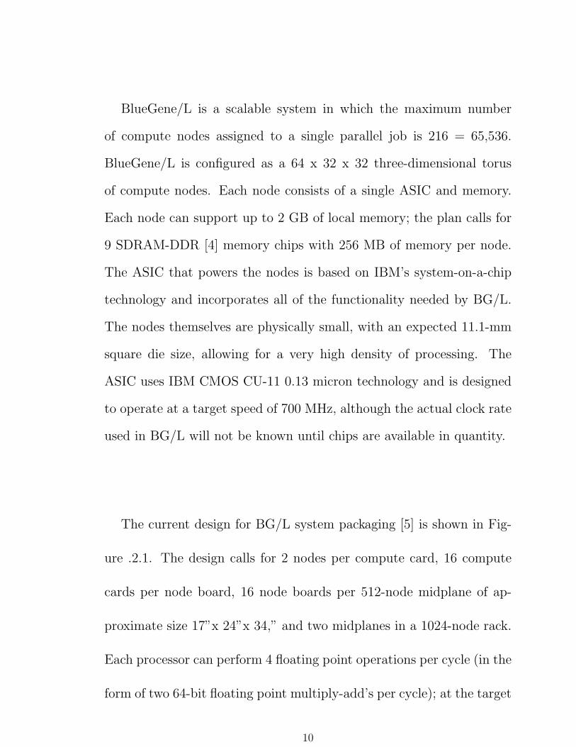
The current design for BG/L system packaging [5] is shown in Fig-
ure .2.1. The design calls for 2 nodes per compute card, 16 compute
cards per node board, 16 node boards per 512-node midplane of ap-
proximate size 17”x 24”x 34,” and two midplanes in a 1024-node rack.
Each processor can perform 4 floating point operations per cycle (in the
form of two 64-bit floating point multiply-add’s per cycle); at the target
10

Figure 2.1: BG/L Packaging
11
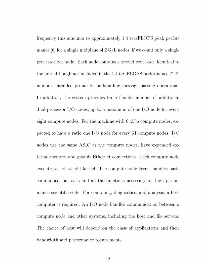
frequency this amounts to approximately 1.4 teraFLOPS peak perfor-
mance [6] for a single midplane of BG/L nodes, if we count only a single
processor per node. Each node contains a second processor, identical to
the first although not included in the 1.4 teraFLOPS performance [7][8]
number, intended primarily for handling message passing operations.
In addition, the system provides for a flexible number of additional
dual-processor I/O nodes, up to a maximum of one I/O node for every
eight compute nodes. For the machine with 65,536 compute nodes, ex-
pected to have a ratio one I/O node for every 64 compute nodes. I/O
nodes use the same ASIC as the compute nodes, have expanded ex-
ternal memory and gigabit Ethernet connections. Each compute node
executes a lightweight kernel. The compute node kernel handles basic
communication tasks and all the functions necessary for high perfor-
mance scientific code. For compiling, diagnostics, and analysis, a host
computer is required. An I/O node handles communication between a
compute node and other systems, including the host and file servers.
The choice of host will depend on the class of applications and their
bandwidth and performance requirements.
12

The nodes are interconnected through five networks: a 3D torus
network for point-to point messaging between compute nodes, a global
combining/broadcast tree for collective operations such as MPI All re-
duce over the entire application, a global barrier and interrupt network,
a Gigabit Ethernet to JTAG network for machine control, and another
Gigabit Ethernet network for connection to other systems, such as hosts
and file systems. For cost and overall system efficiency, compute nodes
are not hooked directly up to the Gigabit Ethernet, but rather use
the global tree for communicating with their I/O nodes, while the I/O
nodes use the Gigabit Ethernet to communicate to other systems.
In addition to the compute ASIC, there is a ”link” ASIC. When
crossing a midplane boundary, BG/L’s torus, global combining tree
and global interrupt signals pass through the BG/L link ASIC. This
ASIC serves two functions. First, it redrives signals over the cables
between BG/L midplanes, improving the high-speed signal shape and
amplitude in the middle of a long, lossy trace-cable-trace connection be-
tween nodes on different midplanes. Second, the link ASIC can redirect
signals between its different ports. This redirection function enables
13

BG/L to be partitioned into multiple, logically separate systems in
which there is no traffic interference between systems. This capability
also enables additional midplanes to be cabled as spares to the sys-
tem and used, as needed, upon failures. Each of the partitions formed
through this manner has its own torus, tree and barrier networks which
are isolated from all traffic from all other partitions on these networks.
2.1 Bluegene Node Overview
The BG/L node ASIC [9], shown in Figure.2.3 includes two standard
PowerPC 440 [10] processing cores, each with a PowerPC 440 FP2 core,
an enhanced ”Double” 64-bit Floating-Point Unit. The 440 is a stan-
dard 32-bit microprocessor core from IBM’s microelectronics division.
This superscalar core is typically used as an embedded processor in
many internal and external customer applications. Since the 440 CPU
core does not implement the necessary hardware to provide SMP sup-
port, the two cores are not L1 cache coherent a lockbox is provided to
allow coherent processor-to-processor communication. Each core has a
small 2 KB L2 cache which is controlled by a data pre-fetch engine, a
14

fast SRAM [4] array for communication between the two cores, an L3
cache directory and 4 MB of associated L3 cache made from embed-
ded DRAM, an integrated external DDR memory controller, a gigabit
Ethernet adapter, a JTAG interface as well as all the network link cut-
through buffers and control. The L2 and L3 are coherent between the
two cores.
In normal operating mode, one CPU/FPU pair is used for compu-
tation while the other is used for messaging. However, there are no
hardware impediments to fully utilizing the second processing element
for algorithms that have simple message passing requirements such as
those with a large compute to communication ratio.
The PowerPC 440 FP2 core [10], consists of a primary side and a
secondary side, each of which is essentially a complete floating-point
unit. Each side has its own 64-bit by 32 element register file, a double-
precision computational datapath and a double-precision storage access
datapath. A single common interface to the host PPC 440 processor is
shared between the sides.
15

Figure 2.2: BlueGene/L node diagram. The bandwidths listed are targets.
16

The primary side is capable of executing standard PowerPC floating-
point instructions [11], and acts as an off-the-shelf PPC 440 FPU [K01].
An enhanced set of instructions include those that are executed solely
on the secondary side, and those that are simultaneously executed on
both sides. While this enhanced set includes SIMD operations, it goes
well beyond the capabilities of traditional SIMD architectures. Here,
a single instruction can initiate a different yet related operation on
different data, in each of the two sides. These operations are per-
formed in lockstep with each other. They have termed these types of
instructions SIMOMD for Single Instruction Multiple Operation Mul-
tiple Data. While Very Long Instruction Word (VLIW) processors can
provide similar capability, we are able to provide it using a short (32
bit) instruction word, avoiding the complexity and required high band-
width of long instruction words.
Another advantage over standard SIMD architectures is the abil-
ity of either of the sides to access data from the other side’s register
17

file. While this saves a lot of swapping when working purely on real
data, its greatest value is in how it simplifies and speeds up complex-
arithmetic operations. Complex data pairs can be stored at the same
register address in the two register files with the real portion residing
in the primary register file, and the imaginary portion residing in the
secondary register file. Newly defined complex arithmetic instructions
take advantage of this data organization.
A quad word (i.e., 128 bits) datapath between the PPC 440s Data
Cache and the PPC 440 FP2 allows for dual data elements (either
double-precision or single precision) to be loaded or stored each cy-
cle. The load and store instructions allow primary and secondary data
elements to be transposed, speeding up matrix manipulations. While
these high bandwidth, low latency instructions were designed to quickly
source or sink data for floating-point operations, they can also be used
by the system as a high speed means of transferring data between mem-
ory locations. This can be especially valuable to the message processor.
18
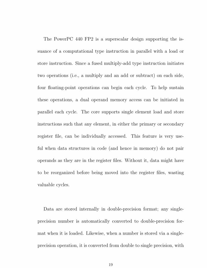
The PowerPC 440 FP2 is a superscalar design supporting the is-
suance of a computational type instruction in parallel with a load or
store instruction. Since a fused multiply-add type instruction initiates
two operations (i.e., a multiply and an add or subtract) on each side,
four floating-point operations can begin each cycle. To help sustain
these operations, a dual operand memory access can be initiated in
parallel each cycle. The core supports single element load and store
instructions such that any element, in either the primary or secondary
register file, can be individually accessed. This feature is very use-
ful when data structures in code (and hence in memory) do not pair
operands as they are in the register files. Without it, data might have
to be reorganized before being moved into the register files, wasting
valuable cycles.
Data are stored internally in double-precision format; any single-
precision number is automatically converted to double-precision for-
mat when it is loaded. Likewise, when a number is stored via a single-
precision operation, it is converted from double to single precision, with
19

the mantissa being truncated as necessary. In the newly defined instruc-
tions, if the double-precision source is too large to be represented as a
single precision value, the returned value is forced to a properly signed
infinity. However, round to single precision instructions are provided so
that an overflowing value can be forced to infinity or the largest single
precision magnitude, based on the rounding mode.
Furthermore, these instructions allow for rounding of the mantissa.
All floating-point calculations are performed internally in double pre-
cision and are rounded in accordance with the mode specified in the
PowerPC defined floating-point status and control register (FPSCR).
The newly defined instructions produce the IEEE-754 specified default
results for all exceptions. Additionally, a non-IEEE mode is provided
for when it is acceptable to flush denormalized results to zero. This
mode is enabled via the FPSCR and it saves the need to renormalize
denormal results when using them as inputs to subsequent calculations.
20
All computational instructions, except for divide and those operat-
ing on denormal operands, execute with a five cycle latency and single
cycle throughput. Division is iterative, producing two quotient bits per
cycle. Division iterations cease when a sufficient number of bits are
generated for the target precision, or the remainder is zero, whichever
occurs first. Faster division can be achieved by employing the highly
accurate (i.e., to one part in 213) reciprocal estimate instructions and
performing software pipelined Newton-Raphson iterations. Similar in-
structions are also provided for reciprocal square root estimates with
the same degree of accuracy.
Library routines and ambitious users can also exploit these enhanced
instructions through assembly language, compiler built-in functions,
and advanced compiler optimization flags. The double FPU can also
be used to advantage by the communications processor, since it permits
high bandwidth access to and from the network hardware.
21

Power is a key issue in such large scale computers, therefore the FPUs
and CPUs are designed for low power consumption. Incorporated tech-
niques range from the use of transistors with low leakage current, to
local clock gating, to the ability to put the FPU or CPU/FPU pair to
sleep. Furthermore, idle computational units are isolated from chang-
ing data so as to avoid unnecessary toggling.
The memory system is being designed for high bandwidth, low la-
tency memory and cache accesses. An L2 hit returns in 6 to 10 processor
cycles, an L3 hit in about 25 cycles, and an L3 miss in about 75 cycles.
L3 misses are serviced by external memory, the system in design has
a 16 byte interface to nine 256Mb SDRAM-DDR devices operating at
a speed of one half or one third of the processor. While peak memory
bandwidths are high, sustained bandwidths will be lower for certain
access patterns, such as a sequence of loads, since the 440 core only
permits three outstanding loads at a time.
22

2.2 Power PC Instruction Set Architecture
Although these categories are not defined by the PowerPC architecture,
the PowerPC instructions [11] can be grouped as follows:
o Integer instructions: These instructions are defined by the UISA.They
include computational and logical instructions.
Integer arithmetic instructions,Integer compare instructions, Logical in-
structions,Integer rotate and shift instructions.
o Floating-point instructions: These instructions, defined by the
UISA, include floating-point computational instructions, as well as in-
structions that manipulate the floating-point status and control register
(FPSCR).
Floating-point arithmetic instructions,Floating-point multiply and add
instructions,Floating-point compare instructions,Floating-point status
and control instructions,Floating-point move instructions,Optional floating-
point instructions.
23

o Load/store instructions: These instructions, defined by the UISA,
include integer and floating-point load and store instructions.
Integer load and store instructions,Integer load and store with byte re-
verse instructions,Integer load and store multiple instructions,Integer
load and store string instructions, Floating-point load and store in-
structions.
o The UISA also provides a set of load/store with reservation instruc-
tions (lwarx and stwcx.) that can be used as primitives for constructing
atomic memory operations. These are grouped under synchronization
instructions. o Synchronization instructions-The UISA and VEA de-
fine instructions for memory synchronizing, especially useful for multi-
processing:
Load and store with reservation instructions,These instructions pro-
vide primitives for synchronization operations such as test and set,
compare and swap, and compare memory. The Synchronize instruc-
tion (sync)-This instruction is useful for synchronizing load and store
operations on a memory bus that is shared by multiple devices.Enforce
In-Order Execution of I/O (eieio) - The eieio instruction provides an
ordering function for the effects of load and store operations executed
by a processor.
24
2.3 Memory Architecture
Figure.2.3 shows the memory architecture of the BLC chip [12][9],
which integrates two 32-bit PPC440 cores, each with an integrated
low-latency, high bandwidth 32-KB L1 data cache and 32-KB L1 in-
struction cache. The L1 data cache is nonblocking. This allows the
subsequent instructions to be executed without having to wait for L1
misses to be resolved. The accesses missing in the L1 cache enter a
limited-size load miss queue. To achieve maximum off-core load band-
width, the load latency from the next level of the memory hierarchy
must be as small as possible to avoid stalls caused by a full miss queue.
This was achieved in the design by adding a 2-KB prefetching buffer
as close to the core as possible, storing data in a high-speed register
file with minimum latency. Because this prefetching buffer also pro-
vides limited caching service, it embodies L2 of the BLC chip cache
hierarchy. They call the complex of one PowerPC processor core, its
FPU, and L2 cache a processing unit (PU). On the next level of the
cache hierarchy, a large, shared L3 cache was implemented. Because of
the relaxed latency requirements beyond the L2 cache, they were able
25
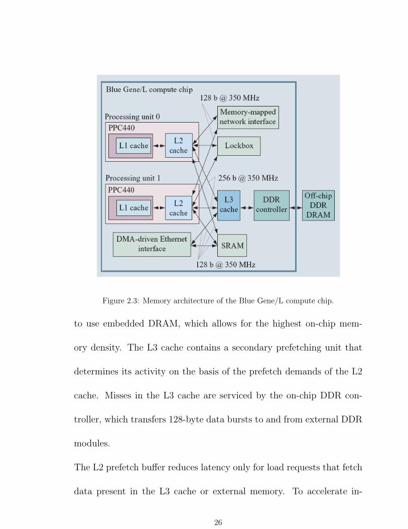
Figure 2.3: Memory architecture of the Blue Gene/L compute chip.
to use embedded DRAM, which allows for the highest on-chip mem-
ory density. The L3 cache contains a secondary prefetching unit that
determines its activity on the basis of the prefetch demands of the L2
cache. Misses in the L3 cache are serviced by the on-chip DDR con-
troller, which transfers 128-byte data bursts to and from external DDR
modules.
The L2 prefetch buffer reduces latency only for load requests that fetch
data present in the L3 cache or external memory. To accelerate in-
26

ter processor communication within a single chip, a low-latency shared
SRAM [4]and a fast synchronization device, called the lockbox, have
been implemented.
In addition to the microprocessors, memory is also accessed by an au-
tonomous DMA controller that offloads the Ethernet data transfers-the
multichannel memory abstraction layer (MCMAL) core. The Gigabit
Ethernet DMA is integrated in the memory subsystem with direct ac-
cess to the SRAM module and main memory via the L3 cache. Memory
mapped control registers allow either processor in a BG/L node to ini-
tialize a DMA transfer while continuing to handle other tasks with very
little overhead.
2.3.1 The PowerPc Core and L1 Cache
The PPC440 hard core serves as the main processing unit in the BLC
chip [9]. It is a dual-issue, out-of-order superscalar processor, designed
to be clocked nominally at 700MHz. In each cycle, the core can launch
one memory operation, either a load or a store. L1 data cache accesses
are nonblocking and allow a 16-byte-wide load or store operation to
27

be completed every cycle. The resulting L1 data bandwidth of 11.2
GB/s per core is available only for L1 cache hits, while the bandwidth
for misses is determined by the PPC440 core memory interface. The
PPC440 core is designed to be used in conjunction with a bus system
that is supposed to be connected to a variety of on-chip components
with a moderate hardware overhead. The memory interface is a 16-
byte-wide processor local bus interface version 4 (PLB4). All compo-
nents connecting to this interface are designed to run at a maximum
frequency of 200 MHz.
Load and store accesses that miss in the L1 cache enter a four en-
try deep miss queue that supports up to three cache line fetches in
flight. When connected to a 200-MHz PLB4 system, the load and store
throughput is limited to 3.2 GB/s by the bus frequency. This band-
width is, in some implementations, even reduced by bus stalls caused
by the latency of memory devices. The maximum off-core bandwidth
is 3.7 GB/s for load accesses with minimal latency and 5.6 GB/s for
store accesses.
The PPC440 core is normally used in single-processor SoCs in which
28
the hardware overhead for keeping the L1 cache coherent with other
DMA masters is not desired. It does not support memory coherency
for L1 cached accesses. As a consequence, memory coherence of the
node has to be managed by software. This constraint imposes addi-
tional software complexity for managing the L1 state, but comes with
the benefit of avoided performance impact caused by cache-snooping
protocols, reduced hardware complexity, and sequential consistency for
L1-uncached memory accesses.
2.3.2 L2 Cache
To minimize the impact of the limited PPC440 load-miss queue, a low-
latency prefetch buffer, the L2 cache, has been implemented. The buffer
attempts to minimize load latency by predicting future load addresses
and fetching data from the next level of the cache hierarchy ahead of
time.
The PLB4 of the PPC440 [10] core is designed to interface with 200-
MHz PLB components, but can be clocked at a much higher rate. In
29

the BLC chip, the PLB interface for instruction fetches is clocked at
processor speed, 700 MHz. This allows the L2 cache to send 16 bytes
to the L1 instruction cache every processor clock. The L1 data PLB
interfaces can also be clocked at processor speed, but the more complex
coherency conditions required to satisfy this port allowed us to operate
the interface at only half processor frequency, 350 MHz. The request
decoding and acknowledgment is executed locally in the L2 cache and
completes in a single 350-MHz cycle. The high interface frequency,
combined with same-cycle acknowledgment and next-cycle data return
for L2 cache hits, results in a sustained streaming data bandwidth close
to the theoretical interface maximum.
When the processor requests a data item, the L2 cache notes the ac-
cess address in an eight-entry history buffer. When a requested address
matches an address in the history buffer or points to the following line,
the L2 cache not only requests the demanded 32-byte-wide L1 cache
line from the L3 cache, but requests four L1 cache lines using a burst
request, assuming that further elements of these lines will be requested
30
in the near future. Later on, when another request demands data from
the burst-fetched memory area, the L2 cache starts to burst-fetch four
L1 cache lines ahead of the current request.
The L2 cache holds up to 15 fully associative prefetch entries of
128-byte width each. It can effectively support up to seven prefetch
streams, since each stream uses two entries: one entry serves the cur-
rent requests from the PPC440 and the other fetches data from the L3
cache.
2.3.3 L3 Cache
Scientific applications are the main application domain for the BG/L
machine. Many scientific applications exhibit a regular, predetermined
access pattern with a high amount of data reuse. To accommodate
the high bandwidth requirements of the cores for applications with a
limited memory footprint, they integrated a large L3 cache on-chip.
Besides SRAM, the IBM CU-11 library also offers embedded DRAM
31

macros [5] in multiples of 128 KB. Although embedded DRAM access
time is much higher than SRAM, it offers three times more density.
SRAM has an access time of slightly more than 2 ns, while access to
an open embedded DRAM page takes about 5 ns. If a page has to
be opened for the embedded DRAM access (low locality of the access
pattern), the page-open and possible page-close operations require an
additional 5 ns each.
The latency of the PPC440 PLB interface alone contributes 14 ns of
latency for an L1 miss or L2 cache hit. The emphasis of the architec-
ture is on a good prefetching performance of the L2 cache with a lower
emphasis on L3 cache latency, assuming that the L3 cache latency al-
lows for uninterrupted prefetch streaming at the maximum bandwidth
defined by the PPC440 core interface. The embedded DRAM latency
is small enough to be hidden by the L2 prefetch, while allowing large
memory footprint processing. As a result, it reduces contention on the
interface to external DDR DRAM and thus also reduces the power con-
sumed by switching I/O cells.
The two memory banks share a four-entry-deep write-combining buffer
32
that collects write requests from all interfaces and combines them into
write accesses of cache line size. This reduces the number of embedded
DRAM write access cycles and enables L3 cache line allocations with-
out creating external DDR traffic. DDR read accesses would normally
be required to establish complete lines before parts of the line content
can be modified by a write.
The PPC440 PLB4 interface requires all requests to return their data
in order. As a consequence, only the oldest entries in the read request
queues are allowed to send data back to the cores. However, in this im-
plementation, all requests present in the read request queues prepare
for a quick completion. All requests queued are performing directory
look-ups, resolving any misses, opening embedded DRAM pages, and
initiating DDR-to-L3 cache prefetch operations while waiting for their
predecessors to return their data to the cores. The small embedded
DRAM page size of four cache lines provides only a limited benefit for
a page-open policy.
DDR-to-L3 cache prefetch operations are initiated upon L2 cache data
33
prefetch requests or by the PPC440 instruction fetch unit. The prefetch
request is an attribute of a regular L3 cache read request, indicating a
high likelihood that the lines following the currently requested line will
be requested in the near future. The L3 cache collects these requests in
its prefetch unit, performs the required directory look-ups, and fetches
the data from DDR if necessary at a low priority. It effectively fetches
ahead of the L2 prefetch with a programmable prefetch depth.
The embedded DRAM of the L3 cache can be statically divided into a
region dedicated to caching and a second region available as static on-
chip memory, the scratchpad memory. Any set of lines can be allocated
as scratchpad memory, which also allows the exclusion of any particular
line from caching operations without further implications. This can be
used to mask defects of the embedded DRAMs that exceed the repair
capabilities of the redundant bitlines and wordlines of the embedded
DRAM macros.
34

2.3.4 Lockbox and SRAM
The latency of the L3 cache cannot be hidden by the L2 cache when
the two PPC440 cores attempt to communicate via memory. To reduce
the latency for standard semaphore operations, barrier synchronization,
and control information exchange, two additional memory-mapped de-
vices have been added to the BLC chip architecture.
The first device is called the lockbox. It is a very small register set with
optimized access and state transition for mutual exclusion semaphores
and barrier operations. It consists of 256 single-bit registers that can be
atomically probed and modified using a standard no cached load oper-
ation. The lockbox unconditionally accepts access requests every cycle
from both processor core units without blocking. In a single cycle, the
state of all accessed registers is atomically updated and returned. The
second device for interprocessor communication is a shared low-latency
SRAM memory device used primarily during initial program load (IPL)
and for low-latency exchange of control information between the two
PPC440 cores. It is an arbitrated unit using a single-port SRAM macro
of 16-byte data width and two bytes ECC. Its low complexity allows it
35
to use a single two-stage pipeline running at 350 MHz that consists of
an arbitration and SRAM macro setup stage and an SRAM access and
ECC checking stage. The SRAM is mapped to the highest addresses
of the memory space, and its content can be accessed directly via the
JTAG interface. This path is used in the primary boot, which loads
boot code into SRAM and then releases the processor cores from reset;
the cores then start fetching instructions from SRAM. The boot code
can either wait for more code to be deposited into SRAM or use the
collective or Ethernet interfaces to load the full program image into
main memory.
2.3.5 Performance of the Memory Subsystem
The memory subsystem of the BLC [7] delivers very high bandwidth
because of its multilevel on-chip cache hierarchy with prefetch capa-
bilities on multiple levels. Figure.4.2(a) shows the read bandwidth for
sequential streams repeatedly accessing a memory area of limited size.
The tests were executed with a fraction of the L1 locked down for the
36

testing infrastructure, allowing only 16 KB of L1 cache to be used in the
test. All cache configurations achieve the maximum L1 hit bandwidth
of 11 GB/s for streams limited to up to 16 KB. Larger streams con-
stantly miss in the L1, reducing the bandwidth to the amount defined
by the latency of the miss-service. The latency of the external DDR
modules allows for only less than 1 GB/s. The lower L3 cache latency
improves the bandwidth to 1.7 GB/s. The L2-cache-based prefetching
in combination with L3-cache prefetching allows a bandwidth of more
than 3.5 MB/s for arbitrary stream sizes.
In Figure.4.2(b), the write bandwidth for different stream sizes and
caching configurations is displayed. In the case of a disabled L1 cache,
all writes are presented on the PPC440 core interface to the next levels
of the memory system and stored into L3. The L3 cache can keep up
with the rate independently of stream size, since its write-combining
buffer forms complete L3 cache lines out of eight subsequent write re-
quests; thus it reduces the number of accesses to embedded DRAM.
37

Figure 2.4: (a) Sequential read bandwidth. (b) Sequential write bandwidth. (c)
Random access latency. (d) DAXPY performance.
38

If the L1 cache is enabled, the write-back strategy of the L1 cache
allows 11 GB/s throughput for streams that fit into L1. For larger
sizes, the accesses cause constant L1 misses, leading to evictions of
modified lines and fetches from the next cache hierarchy to complete
writes to form full L1 cache lines (write allocation). For streams up to
the size of the L3 cache, the PPC440 read interface limits the band-
width to 3.7 GB/s. As soon as the L3 cache begins to evict lines for
even larger streams, the constant alterations of read and write traffic
to DDR, along with bank collisions in the DDR modules, reduce the
write performance further, down to 1.6 GB/s.
In Figure.4.2(c), the load latency is shown for random reads from
a limited memory area. Since the random reads access different em-
bedded DRAM pages with a very high probability when hitting in the
L3 cache, the latency does not reflect the page mode benefit exploited
when streaming data. Note that the latency for accesses with L3 cache
disabled is lower than for L3 cache misses, because no directory look-
ups have to be performed in the uncached case.
39

Figure.4.2(d) shows the achievable floating-point performance for the
L1 Basic Linear Algebra Subprograms routine DAXPY, measured in
floating-point operations per 700-MHz processor cycle. For each fused
multiply-add (FMA) operation pair (two flops per cycle), 16 bytes must
be loaded from memory and eight bytes must be stored back. For a
floating-point performance of one flop per cycle, i.e., 700 Mflops, an
aggregate load/store bandwidth of 12 bytes per cycle, i.e., 8.4 GB/s, is
required.
For stream sizes that fit into L1, the memory bandwidth approaches
the theoretical limit of 11.2 GB/s. Single-core streams of up to 4 MB
fit into the L3 cache and achieve a bandwidth of 4.3 GB/s, while dual-
core performance for streams of up to 2 MB each achieves 3.7 GB/s
because of banking conflicts within the L3 cache. For even larger stream
sizes, the performance drops further as a result of bank collisions in the
external DDR memory modules.
40

2.4 Interconnection Network in Bluegene
One of the most important features of a massively parallel supercom-
puter is the network that connects the processors together and allows
the machine to operate as a large coherent entity. In Blue Gene*/L
(BG/L), the primary network for point-to-point messaging is a three-
dimensional (3D) torus [13] network. A general structure of the Torus
Router is given in Fig.2.5.Nodes are arranged in a 3D cubic grid in which
each node is connected to its six nearest neighbors with high-speed ded-
icated links. A torus was chosen because it provides high-bandwidth
nearest-neighbor connectivity while also allowing construction of a net-
work without edges. This yields a cost-effective interconnect that is
scalable and directly applicable to many scientific and data-intensive
problems.
A torus can be constructed without long cables by connecting each
rack with its next to nearest neighbor along each x, y, or z direction
and then wrapping back in a similar fashion. For example, if there are
six racks in one dimension, the racks are cabled in the order of 1, 3, 5,
6, 4, 2, and 1. Also, because the network switch is integrated into the
41
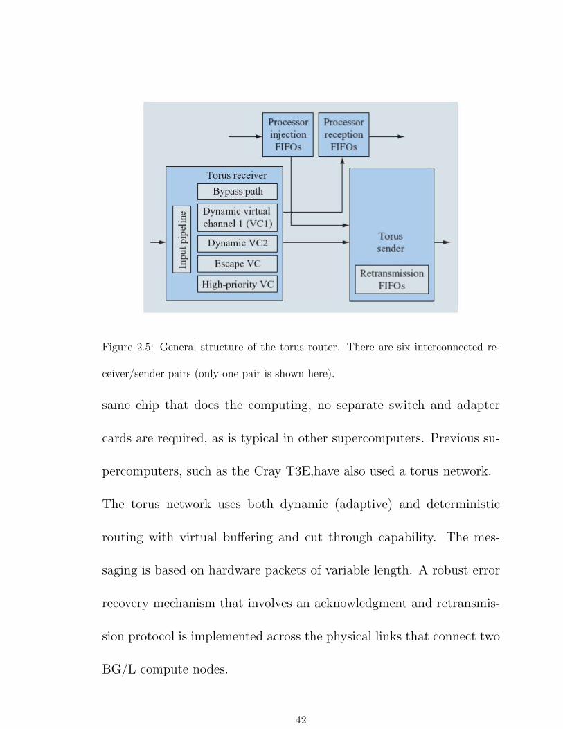
Figure 2.5: General structure of the torus router. There are six interconnected re-
ceiver/sender pairs (only one pair is shown here).
same chip that does the computing, no separate switch and adapter
cards are required, as is typical in other supercomputers. Previous su-
percomputers, such as the Cray T3E,have also used a torus network.
The torus network uses both dynamic (adaptive) and deterministic
routing with virtual buffering and cut through capability. The mes-
saging is based on hardware packets of variable length. A robust error
recovery mechanism that involves an acknowledgment and retransmis-
sion protocol is implemented across the physical links that connect two
BG/L compute nodes.
42
Chapter 3
The Architecture of the Bluegene
Emulator
The overall architecture of the Bluegene has been classified into four
functional stages. The application that is to be executed on the em-
ulated Bluegene has to be partitioned into the constituent algorithms
and these algorithms have to be mapped to the different nodes. This
is done with a coarse level dependency analysis in which there may be
a data dependency between the instructions of the modules or a con-
trol dependency.Based on the dependency they are mapped on to the
different nodes using the conventional Simulated Annealing algorithm.
The Simulated Annealing algorithm is applied to balance both com-
43

INPUTAPPLICATION
COARSE LEVELPARTITIONER
HOST MAP UNIT
DIASSEMBLER
NODE LEVELEMULATOR
LINUX CLUSTER
Figure 3.1: Architecture of the Emulator
44

putation and the communication. But the priority is always given to
computation in situations of conflicts between computation and com-
munication.
After the mapping at the cluster level is complete, the modules assigned
to the node level have to be disassembled into the respective PowerPC
440 assembly. This PowerPC 440 assembly at each node goes through
node level emulation on top of the Linux cluster.
The communication between the different nodes is modeled as the com-
munication between the different processes wherein each process acts
as a node. This communication in the Linux cluster is instituted by
means of the Message Passing Interface. A detailed diagrammatic rep-
resentation of the architecture is given above in Figure.3.1.
45
Chapter 4
Description of the Emulator
Modules
4.1 Memory Access Module
To emulate the execution of any library at the node level, the delay
involved in the memory access plays a vital role. The memory hierarchy
of BlueGene [9] has been analyzed and a brief overview of which is
presented in the previous section. The overall delay can be modeled
using a stochastic distribution which is based on the different access
times at different levels of the hierarchy. The memory access time
depends on the availability of the data being searched for at the different
levels of the cache. For example, the data when available in L1 cache,
46

L1 Cache
µ1,σ1
L2 Cache
µ2,σ2
L3 Cache
µ3,σ3
Figure 4.1: Stochastic Distribution to determine the overall memory access Delay
the access delay will be minimal. There may be cases in which there
may be misses at L1, L2, L3 caches resulting in the local SRAM access.
Thus considering the memory hierarchy, the size of the memory at
different levels of the hierarchy, the replacement algorithm used, the
access time at different levels, a distribution is arrived at as shown in
fig.4.1. Thus it is based on this distribution the delay for memory access
is incorporated into the emulation.
4.2 Branch Prediction Module
A Branch History Table (BHT) maintains a record of recent outcomes
for conditional branches (taken or not taken). Many implementa-
tions have branch history tables that associate 2 bits with each con-
47

ditional branch in the table. The four states of the 2-bit code stand
for strongly taken, weakly taken, weakly not taken, and strongly not
taken. Figure.4.2shows the relationship between these four states. A
conditional branch whose BHT entry is taken, either strongly or weakly,
is predicted taken. Likewise, any branch whose entry is not taken, is
predicted not taken. If a branch is strongly taken, for example, and
is mispredicted once, the state becomes weakly taken. On the next
encounter of the branch, it is still predicted taken. Requiring two
mispredictions to reverse the prediction for a branch prevents a sin-
gle anomalous event from modifying the prediction. If the branch is
mispredicted twice, however, the prediction reverses. The PowerPC
architecture [10] offers no means for the operating system to commu-
nicate a context switch to the dynamic branch prediction hardware,
so the saved history may represent another context. The processor
will correctly execute the code, but additional misprediction and the
associated degradation of performance may be introduced.
48

Figure 4.2: Relationship Between the states of Branch Prediction
Figure 4.3: 3-D Torus Topology Interconnection in Bluegene
49

4.3 Network Module
The 3D-Torus topology [13] used by BlueGene is considered to be one
of the best topologies for executing applications of varying communica-
tional complexity. The table gives the different performance metrics of
a few networks in which it is clearly evident that 3D Torus [13] is the
best topology which has maximum connectivity and minimum diam-
eter aiding in execution of highly dense applications. When it comes
to mapping of an application, there are two main problems to be ad-
dressed namely the Load balancing and the communication balancing.
It is always a trade-off between load and communication that need to
be achieved for the most efficient execution of the application. Load
balancing is the process of checking whether the different nodes have
equally allocated computations i.e., neither of the nodes are neither
overloads nor they are idle. Similarly, interconnects between the nodes
should also be equally sharing the communication overhead of the clus-
ter. For this purpose, normally algorithms are given a spread restriction
based on the size of the algorithm. The network is emulated as the first
phase of the project in which Simulated Annealing is employed to map
50
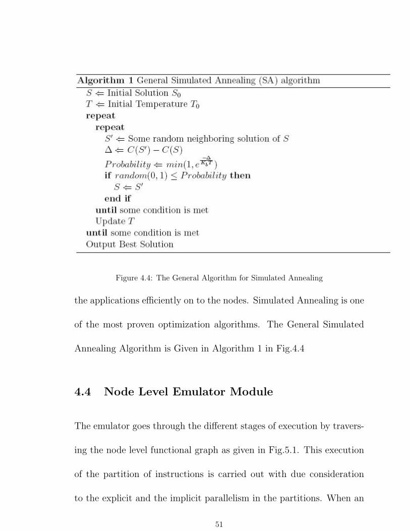
Figure 4.4: The General Algorithm for Simulated Annealing
the applications efficiently on to the nodes. Simulated Annealing is one
of the most proven optimization algorithms. The General Simulated
Annealing Algorithm is Given in Algorithm 1 in Fig.4.4
4.4 Node Level Emulator Module
The emulator goes through the different stages of execution by travers-
ing the node level functional graph as given in Fig.5.1. This execution
of the partition of instructions is carried out with due consideration
to the explicit and the implicit parallelism in the partitions. When an
51
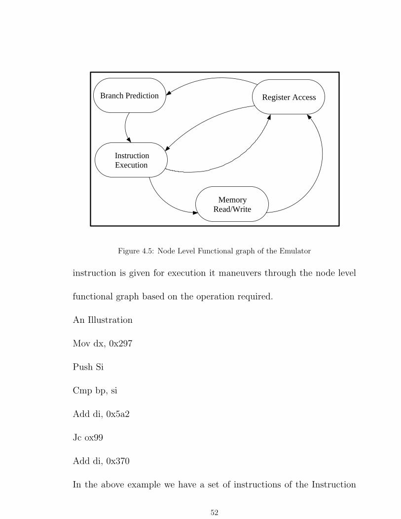
Branch Prediction
InstructionExecution
MemoryRead/Write
Register Access
Figure 4.5: Node Level Functional graph of the Emulator
instruction is given for execution it maneuvers through the node level
functional graph based on the operation required.
An Illustration
Mov dx, 0x297
Push Si
Cmp bp, si
Add di, 0x5a2
Jc ox99
Add di, 0x370
In the above example we have a set of instructions of the Instruction
52

Set Architecture of PowerPC 440 [10]. When the first instruction from
the above block is given for execution (i.e.) the MOV instruction a
memory access takes place then followed by a register access for the
push instruction. The jump instruction enters the branch prediction
block and then based on the branch predicted by the BPU, proceeds
with execution of the other instructions. The execution of the instruc-
tions such as the Cmp, Add, etc. is taken care of by the instruction
execution block which carries out the actual execution. Thus when it
comes to modeling the delay involved in execution of each instruction,
it is just a graph traversal in which the different states like memory
access, register access, branch prediction are the different nodes of the
graph and the delay at each stage gets added to the delay for the exe-
cution of the instruction. This instruction delay is incorporated in the
emulation in such a way that when an instruction gets triggered it waits
for ’n’ Bluegene clock cycles until it is marked finished where the value
of ’n’ is calculated in the above mentioned process. In the process of
approximating the delay involved in each instruction, the instruction
set of PowerPC 440 [11] was analyzed. Primarily, the instructions were
53

classified based on the Instruction type and then based on the address-
ing mode used by the instruction.
4.5 Scalability of the Emulator
Scale is recognized as a primary scalability factor. Proximity, mea-
sured by communication delays, is recognized as a dominant factor in
algorithm design. In general, algorithms and techniques those work at
small scale degenerate in non-obvious ways at large scale. A topology
dependent scheme or an algorithm which is system size dependent are
not scalable. The performance of a parallel algorithm is influenced by
communicational delays, system architecture, and system size. Thus
an algorithm may perform well given a certain number of processors
and architecture, but its performance degrades as either changes. Ide-
ally, the performance should increase linearly with the system size, but
in reality performance degrades with the growth of the system. For
example, say a Matrix Multiplication algorithm of say a fixed problem
size executes on a mesh. When the architecture and the algorithm are
54
scaled simultaneously, (ie)., the number of processors in the mesh is
increased and the problem size of the matrix to be multiplied is in-
creased, the performance remains constant. Thus it can be concluded
that matrix multiplication is scalable with mesh. But, we find that LU
decomposition is not scalable with a mesh rather most of the parallel
algorithms are scalable with the 3D Torus topology [13]. This was the
main reason that most of the super computers which top the list are
built using the 3-D Torus or the Fat tree topology. IBM Blue Gene
recently doubled its size from 65,536 nodes to 1, 31,000 nodes with a
60% increase in performance [7] which was possible only because of this
reason.
Scalability may be defined as ”the system’s ability to increase speedup
as the number of processors increase”. Thus to achieve the same scal-
ability of IBM Blue Gene, the emulator is also designed in such a way
that when the number of Linux nodes are increased (architecture scal-
ability) and simultaneously the number of algorithms and the problem
size are also increased, it gives nearly the same scaling factor as of IBM
Blue Gene.
55
4.6 Checkpointing and Rollback
Check pointing is the technique that generally allows a process to save
its state at regular intervals during normal execution so that it can be
restored later after a failure to reduce the amount of lost work. Using
checkpoints, when a fault occurs, the affected process can simply be
restarted from the last saved checkpoint rather than from the begin-
ning. Since the grand challenge applications that are executed on super
computers run for long time, this process of check pointing is necessary
to avoid transient faults. Long-running applications are generally num-
ber crunching programs that run for several days or weeks and for which
a restart from the scratch due to fault may be unacceptable. In the
process of check pointing two important characteristics need to be fixed
up namely the check pointing interval and also which all variables that
need to be check pointed. The check pointing interval of the emulator
is kept to be a variable so that it can be set based on the application
that is to be executed on the emulator. This check pointing is also
useful in the case of power failure during the process of execution.
56
4.7 The LinPack Benchmark
The LINPACK Benchmark [14] was introduced by Jack Dongarra. The
benchmark used in the LINPACK Benchmark is to solve a dense system
of linear equations. The LINPACK algorithm solves a linear system of
order n; by solving for Ax = b, where A is a matrix of size n n, x is
a column vector of n unknowns and b is a column vector of n known.
The algorithm proceeds by computing the LU factorization with row
partial pivoting of the n n + 1 coefficient matrix [Ab] = [[L, U] y].
There are many LINPACK packages available to estimate performance
of processors. Here a High Performance LINPACK (HPL) package has
been implemented, as it has been used for the top 500 supercomputers.
The package implements block cyclic data distribution across proces-
sors for good load balancing. Figure gives an idea of how a block cyclic
distribution looks like. This performance does not reflect the overall
performance of a given system, as no single number ever can. It does,
however, reflect the performance of a dedicated system for solving a
dense system of linear equations. Since the problem is very regular,
the performance achieved is quite high, and the performance numbers
57

give a good correction of peak performance. By measuring the ac-
tual performance for different problem sizes n, a user can get not only
the maximal achieved performance Rmax for the problem size Nmax
but also the problem size N1/2 where half of the performance Rmax
is achieved. These numbers together with the theoretical peak per-
formance Rpeak are the numbers given in the TOP500 [15] listings of
supercomputers.
58
Chapter 5
The Overall Emulator Flow
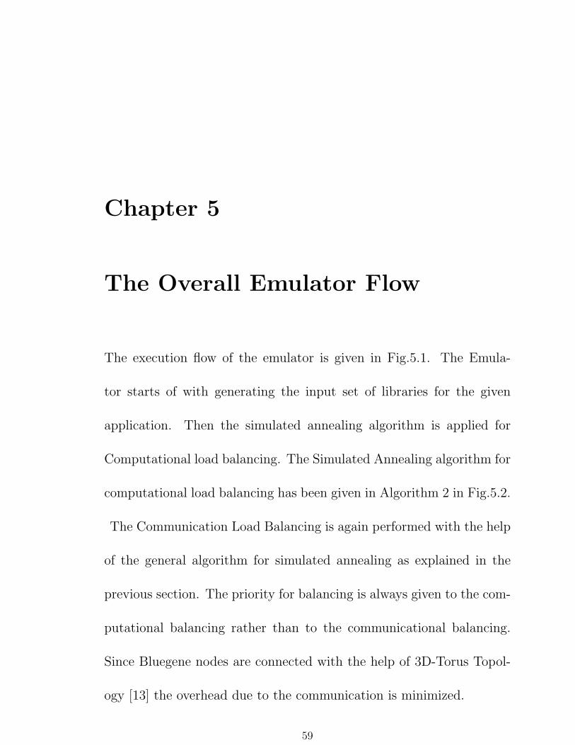
The execution flow of the emulator is given in Fig.5.1. The Emula-
tor starts of with generating the input set of libraries for the given
application. Then the simulated annealing algorithm is applied for
Computational load balancing. The Simulated Annealing algorithm for
computational load balancing has been given in Algorithm 2 in Fig.5.2.
The Communication Load Balancing is again performed with the help
of the general algorithm for simulated annealing as explained in the
previous section. The priority for balancing is always given to the com-
putational balancing rather than to the communicational balancing.
Since Bluegene nodes are connected with the help of 3D-Torus Topol-
ogy [13] the overhead due to the communication is minimized.
59
START
GENERATINGLIBRARIES OFAPPLICATIONS
SIMULATEDANNEALING FOR
LOADBALANCING
SIMULATEDANNEALING FOR
COMMUNICATIONBALANCING
CHECK POINTINGAND ROLLBACK
ISSUER
NODE LEVELEMULATION
IF FINISHEDFLAG SETFOR ALL
LIBRARIES
STOP
NO
YES
Figure 5.1: Emulator Execution Flow Diagram
60

Figure 5.2: Simulated Annealing Algorithm For Computational Balancing
61

Since there is chance of the system to get shutoff during the execution
of the application or there might be situations where unidentified ex-
ceptions might occur. To avoid such situations there is a need for saving
the context and rolling back the execution from the nearest check point.
The issuer performs the job of issuing the set of instructions for execu-
tion in the node-level emulator. The node-level emulator incorporates
the corresponding delay associated with the functional unit and thereby
creating real-time execution environment.
62
Chapter 6
Message Passing Interface(MPI)
The Message Passing Interface (MPI) [16] [17] [18] is a portable message-
passing standard that facilitates the development of parallel applica-
tions and libraries. The standard defines the syntax and semantics
of a core of library routines useful to a wide range of users writing
portable message-passing programs in Fortran 77 or C. MPI also forms
a possible target for compilers of languages such as High Performance
Fortran. Commercial and free, public-domain implementations of MPI
already exist. These run on both tightly-coupled, massively-parallel
machines (MPPs), and on networks of workstations (NOWs). MPI is
used to specify the communication between a set of processes forming
a concurrent program. We use message-passing paradigm because of
63

its wide portability and scalability. It is easily compatible with both
distributed-memory Multicomputer and shared-memory multiproces-
sors, NOWs, and combinations of these elements. Message passing will
not be made obsolete by increases in network speeds or by architectures
combining shared and distributed-memory components.
Message Passing Interface Specifies the Following:
Point to point communications, that is, messages between pairs of
processes.
Collective communications: communication or synchronization opera-
tions that involve entire groups of processes.
Process groups: how they are used and manipulated.
Communicators: a mechanism for providing separate communication
scopes for modules or libraries. Each communicator specifies a distinct
name space for processes, a distinct communication context for mes-
sages and may carry additional, scope-specific information.
Process topologies: functions that allow the convenient manipulation of
process labels, when the processes are regarded as forming a particular
topology, such as a Cartesian grid.
64
Bindings for Fortran 77 and ANSI C: MPI was designed so that versions
of it in both C and Fortran had straightforward syntax. In fact, the
detailed form of the interface in these two languages is specified and is
part of the standard.
Profiling interface: the interface is designed so that runtime profiling
or performance-monitoring tools can be joined to the message-passing
system. It is not necessary to have access to the MPI source to do this
and hence, portable profiling systems can be easily constructed.
Environmental management and inquiry functions: these functions give
a portable timer, some system-querying capabilities, and the ability to
influence error behavior and error-handling functions.
65
Chapter 7
Cluster Configuration
7.1 Node and Network Requirements
A Minimum of 2 nodes is required to set the cluster but more the
number of nodes more powerful the cluster. All nodes should be lat-
est versions of Intel Pentium, AMD Athlon or PowerPC processors.
Each system should have a minimum Random Access Memory (RAM)
Capacity of 256MB.It would be highly impossible to run problems of
higher problem size on a system with very poor RAM capacity since
the main memory cannot hold high end applications of very large size.
A switch is a minimum requirement to set up a parallel environment.
More the number of pins in the switch more are the number of nodes
66
that can be connected. Ethernet cords are required to connect the
nodes with the switch.
7.2 Operating System Requirement
Their goal in developing the system software for BG/L has been to cre-
ate an environment which looks familiar and also delivers high levels of
application performance. The applications get a feel of executing in a
Unix-like environment. The approach adopted is to split the operating
system functionality between compute and I/O nodes. Each compute
node is dedicated to the execution of a single application process. The
I/O node provides the physical interface to the file system. The I/O
nodes are also available to run processes which facilitate the control,
bring-up, job launch and debug of the full BlueGene/L machine. This
approach allows the compute node software to be kept very simple.
The compute node operating system, also called the BlueGene/L
compute node kernel, is a simple, lightweight, single-user operating
67
system that supports execution of a single dual-threaded application
compute process. Each thread of the compute process is bound to
one of the processors in the compute node. The compute node ker-
nel is complemented by a user-level runtime library that provides the
compute process with direct access to the torus and tree networks.
Together, kernel and runtime library implement compute node to com-
pute node communication through the torus and compute node-to-I/O
node communication through the tree. The compute node-to-compute
node communication is intended for exchange of data by the applica-
tion. Compute node-to-I/O node communication is used primarily for
extending the compute process into an I/O node, so that it can perform
services available only in that node.
The lightweight kernel approach for the compute node was motivated
by the Puma and Cougar kernels at Sandia National Laboratory and
the University of New Mexico. The BG/L compute kernel provides a
single and static virtual address space to one running compute process.
Because of its single-process nature, the BG/L compute kernel does not
68

need to implement any context switching. It does not support demand
paging and exploits large pages to ensure complete TLB coverage for
the application’s address space. This approach results in the applica-
tion process receiving full resource utilization.
I/O nodes are expected to run the Linux operating system, support-
ing the execution of multiple processes. Only system software executes
on the I/O nodes, no application code. The purpose of the I/O nodes
during application execution is to complement the compute node parti-
tion with services that are not provided by the compute node software.
I/O nodes provide an actual file system to the running applications.
They also provide socket connections to processes in other systems.
When a compute process in a compute node performs an I/O opera-
tion (on a file or a socket), that I/O operation (e.g., a read or a write) is
shipped through the tree network to a service process in the I/O node.
That service process then issues the operation against the I/O node op-
erating system. The results of the operation (e.g., return code in case
of a write, actual data in case of a read) are shipped back to the origi-
69
nating compute node. The I/O node also performs process authentica-
tion, accounting, and authorization on behalf of its compute nodes.I/O
nodes also provide debugging capability for user applications. Debug-
gers running on an I/O node can debug application processes running
on compute nodes. In this case, the hopping occurs in the opposite di-
rection. Debugging operations performed on the I/O node are shipped
to the compute node for execution against a compute process. Results
are shipped back to the debugger in the I/O node.
7.3 Network Configuration
The network address of the system has to be configured using the hosts
file in the ’etc’ folder of the linux file system. Each system can be
assigned IP address by the configuring the Ethernet present in the net-
work. The IP addresses of all the systems present in the cluster must
be in the hosts file. Alias names can be assigned to each node for un-
complicated identification.
70

7.4 Local Area Multicomputer(LAM)
The LAM/MPI normally comes with the installation of any Linux ver-
sions after Red hat 9.0. The LAM comes in two version LAM 7.0.6
and the LAM 7.1.1.Two systems connected in a parallel environment
must have the same version of LAM, if not this can lead to compati-
bility problems. The LAM (Local Area Multicomputer) with the latest
version MPI 2.0 comes with Fedora Core 3 and 4.
LAM is an MPI programming environment and development system
for a message-passing parallel machine constituted with heterogeneous
UNIX computers on a network. With LAM, a dedicated cluster or an
existing network computing infrastructure can act as one parallel com-
puter solving one compute-intensive problem. LAM emphasizes pro-
ductivity in the application development cycle with extensive control
and monitoring functionality. The user can easily debug the common
errors in parallel programming and is well equipped to diagnose more
difficult problems. LAM features a full implementation of the MPI
communication standard.
71
7.5 LAM Configuration
The LAM Configuration is done with the help of the recon tool provided
by LAM. The recon tests the various nodes in the cluster to ensure that
LAM can be started in the system. In order for LAM to be started on
a remote UNIX machine, several requirements have to be fulfilled:
1) The machine must be reachable via the network. 2) The user
must be able to remotely execute on the machine with the default
remote shell program that was chosen when LAM was configured. This
is usually rsh(1), but any remote shell program is acceptable (such as
ssh(1), etc.). Note that remote host permission must be configured
such that the remote shell program will not ask for a password when a
command is invoked on remote host. 3) The remote user shell must have
a search path that will locate LAM executables. 4) The remote shell
startup file must not print anything to standard error when invoked
non-interactively.
If any of these requirements is not met for any machine declared
in bhost, LAM will not be able to start. By running recon first, the
user will be able to quickly identify and correct problems in the setup
72
that would inhibit LAM from starting. The local machine where recon
is invoked must be one of the machines specified in bhost. The bhost
(lamhosts) file is a LAM boot schema written in the host file syntax.
Instead of the command line, a boot schema can be specified in the
LAMBHOST environment variable. Otherwise a default file, bhost.def,
is used. LAM searches for lamhosts first in the local directory and
then in the installation directory under etc/.recon tests each machine
defined in lamhosts by attempting to execute on it the tkill command
using its ”pretend” option (no action is taken). This test, if successful,
indicates that all the requirements listed above are met, and thus LAM
can be started on the machine. If the attempt is successful, the next
machine is checked. In case the attempt fails, a descriptive error mes-
sage is displayed and recon stops unless the -a option is used, in which
case recon continues checking the remaining machines. If recon takes
a long time to finish successfully, this will be a good indication to the
user that the LAM system to be started has slow communication links
or heavily loaded machines, and it might be preferable to exclude or
replace some of the machines in the system.
73
EXAMPLES
recon -v lamhosts
Check if LAM can be started on all the UNIX machines described in
the boot schema lamhosts.
Report about important steps as they are done
-v be verbose.
-x Run in fault tolerant mode.
-H Do not display the command header.
7.6 Starting a LAM Multicomputer
Once the LAM package is installed in the system the MPI has to be
configured on all the nodes after which the LAM has to be started in all
the nodes such that the environment is made ready to execute a MPI
code.
lamboot is used to start a LAM multicomputer. The lamboot tool
starts the LAM software on each of the machines specified in the boot
schema, bhost. The boot schema specifies the hostnames of nodes to
74
be used in the run-time MPI environment, and optionally lists how
CPUs LAM may be used on each node. The user may wish to first run
the recon tool to verify that LAM can be started. Starting LAM is a
three step procedure. In the first step, hboot(1) is invoked on each of
the specified machines. Then each machine allocates a dynamic port
and communicates it back to lamboot which collects them.In the third
step, lamboot gives each machine the list of machines/ports in order to
form a fully connected topology. If any machine was not able to start,
or if a timeout period expires before the first step completes, lamboot
invokes wipe to terminate LAM and reports the error. The bhost file
is a LAM boot schema written in the host file syntax. Instead of the
command line, a boot schema can be specified in the LAMBHOST envi-
ronment variable. Otherwise a default files, lambhost.def, is used. LAM
searches for bhost first in the local directory and then in the installation
directory under etc/. In addition, lamboot uses a process schema for
the individual LAM nodes. A process schema is a description of the
processes which constitute the operating system on a node. In general,
the system administrator maintains this file, LAM/MPI users will gen-
75
erally not need to change this file. It is also possible for the user to
customize the LAM software with a private process schema. Lamboot
will resolve all names in bhost on the node in which lamboot was in-
voked (the origin node). After that, LAM will only use IPaddresses,
not names. Specifically, the name resolution configuration on all other
nodes is not used. Hence, the origin node must be able to resolve all
the names in bhost to addresses that are reachable by all other nodes.
EXAMPLES
lamboot -v lamhosts
Start LAM on the machines described in the default boot schema. Re-
port about important steps as they are done.
lamboot -d hostfile
Start LAM on the machines described in file hostfile.Provide Incredibly
detailed reports on what is happening at each stage in the boot process.
lamboot mynodes
Start LAM on the machines described in the boot schema mynodes.
76
7.7 Compiling and Executing a MPI/C Code
The Normal Syntax to compile a C code in the Linux environment is
that using the gcc compiler. But when the system uses MPI [18], the
libraries for MPI also have to be compiled . But if this has to be done
manually it would be very tedious. So LAM provides a simple method-
ology for this
mpicc filename.c -o outputfile
This particular syntax compiles the set of LAM libraries along with the
user written code. So this eliminates the manual overhead involved.
The Next part in this process involves the execution of the output file.
mpirun -np numberofnodes outputfile
This command executes the compiled code with the specified number
of nodes or processes.
7.8 Emulation Results
The graph shown in Fig.7.1depicts the amount of load or instructions
77
to get executed in a every bluegene node in a given clock cycle in terms
of 128 bit additions.This is one kind of such results which aids us in
deciding the static schedule, such that there is maximum resource uti-
lization. With the help of the values the peak performance can be
computed with the relation
peak performance = (Number of instructions/clock cycle) * Frequency
The observed peak performance from the emulation was 53.8Gflops.
The graph shown in Fig.7.2 depicts the communicational load in-
volved in the emulated Bluegene system.The X axis specifies the clock
cycles involved followed by the y axis depicting the node and the z-axis
specifying the communicational load.The Communication load is given
in terms of the queue length associated with each node.
78
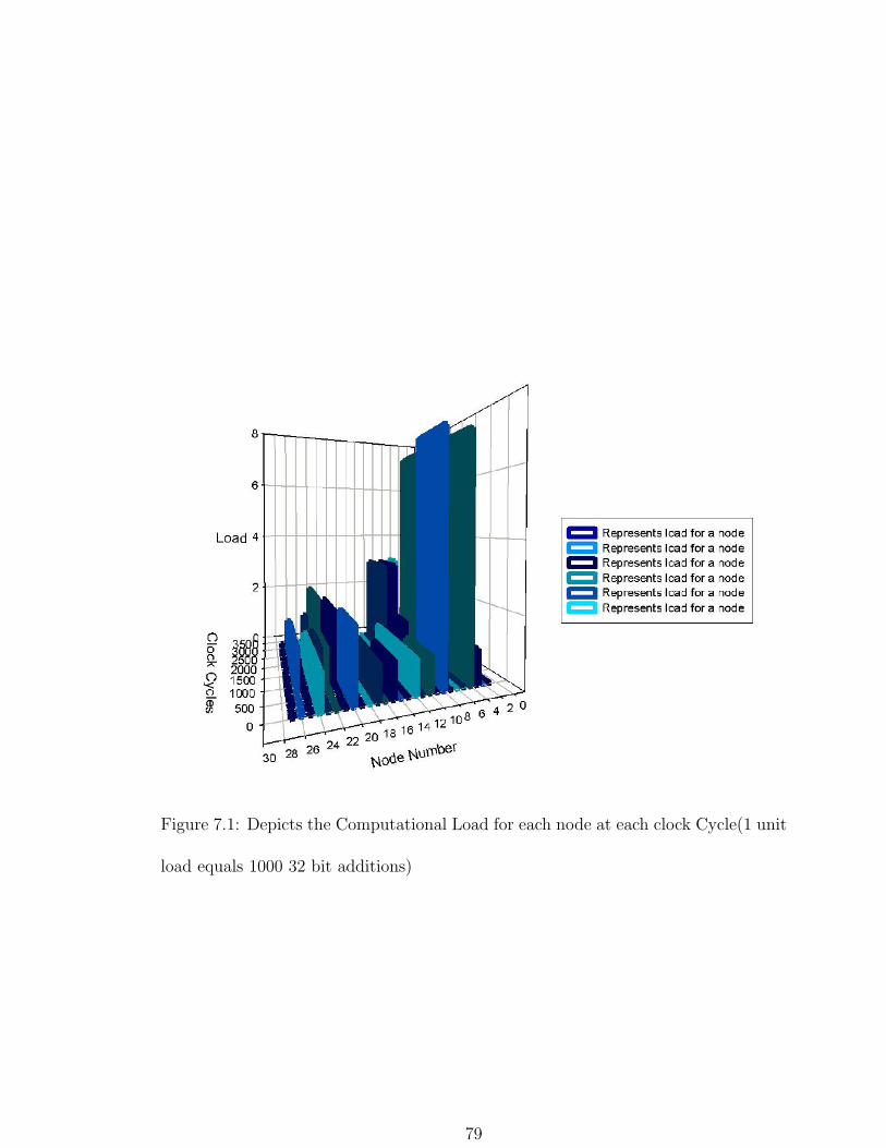
Figure 7.1: Depicts the Computational Load for each node at each clock Cycle(1 unit
load equals 1000 32 bit additions)
79

Figure 7.2: Depicts the Communicational Load for each node at each clock Cycle
80
Bibliography
[1] M. Warren W. Feng and E. Weigle. The bladed beowulf: A cost-
effective alternative to traditional beowulfs. 4th IEEE Interna-
tional Conference on Cluster Computing (IEEE Cluster), Septem-
ber 2002.
[2] P Kogge, T sterling, J Brockman, and G Gao. Processing in mem-
ory : Chip to petaflops. International Symposium on Computer
Architecture ,ISCA ’97, June 1997.
[3] http://www.sc conference.org.
[4] Cypress semiconductor corporation. Fast SRAM Architectures,
1998.
[5] T. M. Cipolla P. G. Crumley A.Gara S. A. Hall G. V. Kopcsay A.
P. Lanzetta L. S. Mok R. Rand R. Swetz T. Takken P. La Rocca
81

C. Marroquin P. R. Germann P. Coteus, H. R. Bickford and M. J.
Jeanson. Packaging the blue gene/l supercomputer. IBM J. Res.
Dev. 49, No. 2/3, 213-248, 2005.
[6] D. K. Beece R. Bellofatto M. A. Blumrich D. Chen M. B.
Dombrowa A. Gara M. E. Giampapa R. A. Haring P. Hei-
delberger D. Hoenicke B. J. Nathanson M. Ohmacht R. Shar-
rar S. Singh B. D.Steinmacher-Burow R. B. Tremaine M. Tsao
A. R.Umamaheshwaran M. E. Wazlowski, N. R. Adiga and
P. Vranas. Verification strategy for the blue gene/l chip. IBM
J. Res. Dev. 49, No. 2/3, 303-318, 2005.
[7] A. Gara J. Gunnels M. Gupta A Henning J. E. Moreira B. Walkup
A. Curioni C. Archer L.Bachega B. Chan B. Curtis M. Brodowicz
S. Brunett E. Upchurch G. Chukkapalli R. Harkness G. Alma si,
S. Chatterjee and W. Pfeiffer. Unlocking the performance of the
bluegene/l supercomputer. Proceedings of SC’04,, 2004.
[8] O. Goldshmidt J. E. Moreira Y. Aridor, T. Domany and E.Shmueli.
Resource allocation and utilization in the bluegene/l supercom-
puter. IBM J. Res. Dev. 49, No. 2/3, 425-436, 2005.
82
[9] S. Bhattacharya A. Gara M. E. Giampapa B. Gopalsamy R. A.
Haring D. Hoenicke D. J. Krolak J. A. Marcella B. J. Nathanson
V. Salapura M. Ohmacht, R. A. Bergamaschi and M. E. Wazlowski.
Blue gene/l compute chip: Memory and ethernet subsystem. IBM
J. Res. Dev. 49, No. 2/3, 255-264, 2005.
[10] IBM. Ibm powerpc 440 embedded core.
[11] IBM. Ibm powerpc 440 microprocessor core programming model
overview. october 2001.
[12] D. Chen G. L.-T. Chiu P. Coteus M. E. Giampapa R. A. Har-
ing P. Heidelberger D. Hoenicke G. V. Kopcsay T. A. Liebsch M.
Ohmacht B. D. Steinmacher-Burow T. Takken P. VranasG Gao
et al A. Gara, M. A. Blumrich. Overview of the blue gene/l sys-
tem architecture. IBM White Paper, April 2005.
[13] D. Chen P. Coteus A. Gara M. E. Giampapa P. Heidelberger S.
Singh B. D.Steinmacher-Burow T. Takken M. Tsao N. R. Adiga,
M. A. Blumrich and P. Vranas. Blue gene/l torus interconnection
network. IBM J. Res. Dev. 49, No. 2/3, 265-276, 2005.
83
[14] Piotr Luszczek Jack J. Dongarra and Antoine Petitet. The linpack
benchmark: Past, present, and future. Concurrency and Compu-
tation:Practice and Experience 15, 1-18.,, 2003.
[15] www.top500.org.
[16] Peter S. Pacheco. Parallel programming with mpi. Morgan Kauf-
mann Publishers, Inc., 1997.
[17] University of Tennessee. Message passing interface forum, ”mpi:
A message-passing interface standard,”. 1995.
[18] J. G. Castan os J. A. Gunnels C. Erway P. Heidelberger X. Mar-
torell J. E. Moreira-K.Pinnow J. Ratterman B. D. Steinmacher-
Burow W. Gropp and B. Toonen G. Alma si, C. Archer. Design
and implementation of message-passing services for the blue gene/l
supercomputer. IBM J. Res. Dev. 49, No. 2/3, 393-406, 2005.
84

Appendix A
The Torus Network in IBM
Bluegene
In this section, the torus network[13] architecture and micro architec-
ture are presented.The torus network router directs variable-size pack-
ets, each n of 32 bytes, where n = 1 to 8 ”chunks.” Messages, such
as those conforming to the Message Passing Interface Standard (MPI),
may consist of many packets that are constructed, sent, and received by
software running on one or both associated BG/L processors. The first
eight bytes of each packet contain link-level protocol information (e.g.,
sequence number); routing information, including destination; virtual
channel and size; and a byte-wide cyclic redundancy check (CRC) that
85
detects header data corruption during transmission.
In addition, a 24-bit CRC is appended to each packet, along with a
one-byte valid indicator. The valid indicator is necessary, since packets
can be forwarded before being entirely received. This CRC permits
checking of each packet as it is sent over each link. A time-out mecha-
nism is used for retransmission of corrupted packets. Use of the eight-
bit packet header CRC is an optimization that permits early detection
of packet header errors because the header CRC is included in the full
packet CRC. The error detection and recovery protocol is similar to
that used in IBM High Performance Switch (HPS) interconnection net-
works and in the HIPPI-6400 standard.
As in the BG/L collective network, each sender (receiver) also main-
tains a 32-bit link-level CRC that includes all data packets sent (re-
ceived) successfully on the link. At the end of a run or at a checkpoint,
each sender link-level CRC matches its corresponding receiver link-level
CRC, thereby providing a mechanism to detect 24-bit packet-level CRC
86

escapes. If not, the results of the run are not to be trusted, and the job
should be restarted from the last checkpoint. Since BG/L is massively
parallel, an efficient, simple, and local error-recovery mechanism was
paramount.
For routing, the header includes six ”hint” bits that indicate the di-
rections in which the packet may be routed. For example, hint bits of
100100 mean that the packet can be routed in the x and y directions.
Either the x or the x hint bits, but not both, may be set. If no x hops
are required, the x hint bits are set to 0. Each node maintains a set
of software-configurable registers that control the torus functions. For
example, a set of registers contains the coordinates of its neighbors.
Hint bits are set to 0 when a packet leaves a node in a direction such
that it will arrive at its destination in that dimension, as determined by
the neighbor coordinate registers. These hint bits appear early in the
header so that arbitration may be efficiently pipelined. The hint bits
can be initialized by either software or hardware; if done by hardware,
a set of two registers per dimension is used to determine the appropri-
87
ate directions. Once the hint bits are set, they cannot be subsequently
changed by software.
These registers can be configured to provide minimal hop routing.
The routing is accomplished entirely by examining the hint bits and vir-
tual channels; i.e., there are no routing tables. Packets may be either
dynamically or deterministically dimension-ordered (xyz) routed. That
is, they can follow a path of least congestion based on other traffic, or
they can be routed on a fixed path. Besides point-to-point packets, a
bit in the header may be set that causes a packet to be broadcast down
any Cartesian dimension and deposited at each node. Hardware broad-
casting in more than one dimension would have greatly complicated
the logic, although deadlocks could have been prevented by broadcast-
ing in the same xyz order. The hardware does not have the capability
to route around ”dead” nodes or links. However, software can set the
hint bits appropriately so that such nodes are avoided; full connectivity
can be maintained when there are up to three noncolinear faulty nodes.
88
The torus logic consists of three major units-a processor interface,
ascend unit, and a receive unit (Figure1). The processor interface con-
sists of network injection and reception FIFOs (queues in which access
is according to the first in, first out rule). Access to these FIFOs is
via the double floating-point unit (FPU) registers; i.e., data is loaded
into the FIFOs via 128-bit memory-mapped stores from a pair of FPU
registers, and data is read from the FIFOs via 128-bit loads to the FPU
registers. There are a total of eight injection FIFOs organized into two
groups: two high-priority (for internode operating system messages)
and six normal-priority FIFOs, which are sufficient for nearest-neighbor
connectivity. Packets in all FIFOs can go out in any direction.
On the reception side, there are again two groups of FIFOs. Each
group contains seven FIFOs, one high priority and one dedicated to
each of the incoming directions. More specifically, there is a dedicated
bus between each receiver and its corresponding reception FIFO. As in
mechanisms in the BG/L collective network, there is a checksum associ-
ated with each injection FIFO; these can be used for fault-isolation and
89
debugging purposes to see whether a node sends the same data onto the
network in two different runs. Watermarks can also be set by software
for the injection and reception FIFOs so that interrupts fire when the
FIFO contents cross the corresponding threshold. For storage, all torus
FIFOs use static random access memory chips (SRAMs) protected by
error checking and correction (ECC), and all internal datapaths are
checked for parity. There is a total of 58 KB of SRAMs.
The datapath for each of the six receivers, as shown in Figure 1, is
composed of an eight-stage input pipeline, four virtual channels (VCs),
and a bypass channel. The input pipeline processes the packet header
on the fly. Multiple VCs help reduce head-of-line blocking, but, since
mesh networks, including tore with dynamic routing, can deadlock, ap-
propriate additional escape VCs are provided. The approach they use
to this problem is similar to the recent, elegant solution, the bubble
escape VC. BG/L has two dynamic VCs, one a bubble escape VC that
can be used both for deadlock prevention and deterministic routing,
and the other a high-priority bubble VC. Dynamic packets can enter
90
the bubble escape VC only if no valid dynamic VCs are available. Each
VC has 1 KB of buffering, enough for four full-sized packets. The by-
pass channel allows packets, under appropriate circumstances, to flow
through a node without entering the VC buffers. This places stringent
timing requirements both on the processing of the header routing in-
formation by the input pipeline and on the routing arbitration by the
receiver arbiters.
A token flow-control algorithm is used to prevent the VC buffers
from overflowing. Each token represents a 32- byte chunk. For sim-
plicity in the arbiters, a VC is marked as unavailable unless space is
available to handle a full-sized packet. However, token counts for pack-
ets on dynamic VCs are incremented and decremented according to the
size of the packet. The bubble rules include the rule that tokens for
one full-sized packet are required for a packet already on the bubble
VC to advance. Tokens for two full-sized packets are required for a
packet to enter the bubble VC upon injection, upon a turn to a new
direction, or when a dynamic VC packet enters the bubble. This rule
91

ensures deadlock-free operation, since buffer space for one packet is
always available after an insertion, and thus some packet can always
move eventually. However, when their simulator deadlocked using this
rule, they discovered that the rule is incorrect for variable-sized pack-
ets. With this rule, the remaining free space for one full-sized packet
can become fragmented, resulting in a potential deadlock. To prevent
this, the bubble rules are modified so that each packet on the bubble
is accounted for as if it were a full-sized packet. BG/L uses dimension-
ordered routing on the bubble VC.
Eight-byte acknowledgment (ack-only) packets or combined token-
acknowledgment (token-ack) packets are returned either when packets
are successfully received or when space has freed up in a VC. Acknowl-
edgments permit the torus send units to delete packets from their re-
transmission FIFOs, which are used in the error recovery protocol. The
send units also arbitrate between requests from the receiver and injec-
tion units.
92

Because of the density of packaging and ASIC-module pin con-
straints, each of the 12 BG/L torus links (six in, six out) is bit-serial.
The torus is internally clocked at a quarter of the rate of the processor.
At the target 700- MHz clock rate, each torus link is 1.4 Gb/s, which
gives 175 MB/s. There are enough internal buses so that each of the six
outgoing and six incoming links can be busy simultaneously; thus, each
node can be sending and receiving 1.05 GB/s. In addition, there are
two transfers buses (paths) coming out of each receiver that connect
with the senders. As a result, a single receiver can have up to four si-
multaneous transfers, e.g., one to its normal processor reception FIFO,
one to the high-priority processor reception FIFO, and two to two dif-
ferent senders. The torus network input and output are byte wide and
are serialized and deserialized by the high-speed signaling units outside
the torus module. The torus internal buses are all 11 bits wide (eight
data, one parity, two control).
Arbitration is distributed and pipelined, but occurs in three basic
phases. It represents tradeoffs among complexity, performance, and the
93
ability to meet timing constraints. In the first phase, a decision is made
for each packet at the head of the injection or VC FIFOs about the di-
rection in which it should preferably move and which VC it should use.
There is only one valid choice for deterministically routed packets, but
there may be many choices for dynamically routed packets. The pre-
ferred direction and VC are selected using a modified join-the-shortest-
queue (JSQ) algorithm, as follows. The senders provide the receivers
and injection FIFOs with a bit that indicates both link and token avail-
ability for each VC in each direction. This bit vector is ANDed with a
bit vector of possible moves constructed from the packet hint bits and
VC. This defines the set of possible and available arbitration requests.
In addition, for each VC the sender provides two bits that indicate one
of four ranges of available downstream tokens. Of all the possible and
available dynamic direction and VC pairs, the packet selects the one
with the most available downstream tokens. Ties are randomly broken.
If no combination of dynamic direction and VC is available, the packet
requests its bubble escape direction and VC pair (if available). If that
is also unavailable, no arbitration request is made for the packet. This
94

is a somewhat simplified description, since data bus availability must
also be taken into account. In addition, when a packet reaches its desti-
nation, the ”direction” requested is simply the corresponding reception
FIFO.
In the second phase, arbitration is required to determine which of
the requesting packets in the receiver wins the right to request, since
each receiver has multiple VC FIFOs in addition to the bypass channel.
If a high priority packet is requesting, it wins. Barring that, a modified
serve the longest queue (SLQ) is used, based on two-bit (four ranges)
FIFO fullness indicators; i.e., the packet from the VC that is fullest as
measured to within the two bits of granularity wins. However, this al-
gorithm cannot always be used, because doing so may completely block
out a VC. Therefore, a certain (programmable) fraction of the arbitra-
tion cycles are designated SLQ cycles, in which the above algorithm is
used, while the remaining cycles select the winner randomly. A packet
on the bypass channel always receives the lowest priority unless it is a
high-priority packet.
95

In the third phase, the requests from the receivers and injection FI-
FOs are presented to the senders. Note that on a given cycle a receiver
presents at most one request to the senders; thus, each sender arbiter
can operate independently. The senders give highest priority to token-
ack or ack-only packets, if any. Barring that, the senders tend to favor
packets already in the network and use a similar modified SLQ algo-
rithm in which there are SLQ cycles and random cycles. In particular,
a certain programmable fraction of cycles (typically 100%) give priority
to packets already in the network, unless the only high-priority packet
requesting is in an injection FIFO. On such cycles, the modified SLQ
algorithm is used. Higher priority can be given to injection packets
by lowering the above in-network priority fraction. On cycles in which
injection packets receive priority, barring in-network high-priority pack-
ets, the modified SLQ algorithm is also used.
This design is complex; the torus unit requires slightly more area
(10.2 mm2 in CU-11) than a PowerPC* 440 processor core and its as-
96
sociated double FPU. The entire torus arbitration is carried out by 44
arbiters on the receiver/processor-injection side and six arbiters on the
sender side. To manage this level of complexity, the design is highly
modular. For example, a single arbiter module was designed that could
serve all VC FIFOs and processor-injection and bypass channels. This
module was then instantiated 38 times.
97
Appendix B
The Operating System
Architecture in Bluegene
Their goal in developing the system software for BG/L has been to cre-
ate an environment which looks familiar and also delivers high levels of
application performance. The applications get a feel of executing in a
Unix-like environment. The approach adopted is to split the operating
system functionality between compute and I/O nodes. Each compute
node is dedicated to the execution of a single application process. The
I/O node provides the physical interface to the file system. The I/O
nodes are also available to run processes which facilitate the control,
bring-up, job launch and debug of the full BlueGene/L machine. This
98

approach allows the compute node software to be kept very simple.
The compute node operating system, also called the BlueGene/L
compute node kernel, is a simple, lightweight, single-user operating
system that supports execution of a single dual-threaded application
compute process. Each thread of the compute process is bound to
one of the processors in the compute node. The compute node ker-
nel is complemented by a user-level runtime library that provides the
compute process with direct access to the torus and tree networks.
Together, kernel and runtime library implement compute node to com-
pute node communication through the torus and compute node-to-I/O
node communication through the tree. The compute node-to-compute
node communication is intended for exchange of data by the applica-
tion. Compute node-to-I/O node communication is used primarily for
extending the compute process into an I/O node, so that it can perform
services available only in that node.
The lightweight kernel approach for the compute node was motivated
99

by the Puma and Cougar kernels at Sandia National Laboratory and
the University of New Mexico. The BG/L compute kernel provides a
single and static virtual address space to one running compute process.
Because of its single-process nature, the BG/L compute kernel does not
need to implement any context switching. It does not support demand
paging and exploits large pages to ensure complete TLB coverage for
the application’s address space. This approach results in the applica-
tion process receiving full resource utilization.
I/O nodes are expected to run the Linux operating system, support-
ing the execution of multiple processes. Only system software executes
on the I/O nodes, no application code. The purpose of the I/O nodes
during application execution is to complement the compute node parti-
tion with services that are not provided by the compute node software.
I/O nodes provide an actual file system to the running applications.
They also provide socket connections to processes in other systems.
When a compute process in a compute node performs an I/O opera-
tion (on a file or a socket), that I/O operation (e.g., a read or a write) is
100
shipped through the tree network to a service process in the I/O node.
That service process then issues the operation against the I/O node op-
erating system. The results of the operation (e.g., return code in case
of a write, actual data in case of a read) are shipped back to the origi-
nating compute node. The I/O node also performs process authentica-
tion, accounting, and authorization on behalf of its compute nodes.I/O
nodes also provide debugging capability for user applications. Debug-
gers running on an I/O node can debug application processes running
on compute nodes. In this case, the hopping occurs in the opposite di-
rection. Debugging operations performed on the I/O node are shipped
to the compute node for execution against a compute process. Results
are shipped back to the debugger in the I/O node.
101