general overview of gan power devices -...
TRANSCRIPT
Confidential
General Overview of GaN Power Devices
Peter Moens

Confidential 2 04/07/2017
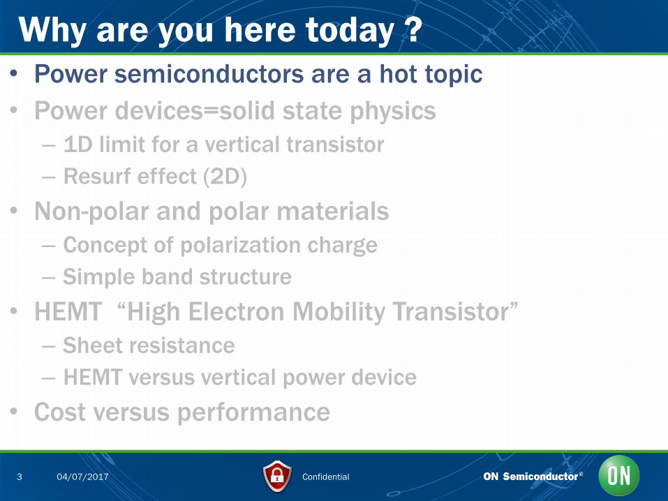
• Power semiconductors are a hot topic
• Power devices=solid state physics
– 1D limit for a vertical transistor
– Resurf effect (2D)
• Non-polar and polar materials
– Concept of polarization charge
– Simple band structure
• HEMT “High Electron Mobility Transistor”
– Sheet resistance
– HEMT versus vertical power device
• Cost versus performance
Why are you here today ?
𝑹𝒐𝒏 =𝟒. 𝑽𝒃𝒅
𝟐
𝑬𝑪𝟑. 𝜺. 𝝁𝑵
𝑹𝒐𝒏 =𝟐. 𝑽𝒃𝒅
𝑬𝑪𝟐. 𝜺. 𝝁𝑵
𝑹𝒐𝒏 =𝟏
𝒒.𝒏𝒔.𝝁𝑵 .
𝑽𝒃𝒅𝟐
𝑬𝒄𝟐
Break
Test
Confidential 3 04/07/2017
• Power semiconductors are a hot topic
• Power devices=solid state physics
– 1D limit for a vertical transistor
– Resurf effect (2D)
• Non-polar and polar materials
– Concept of polarization charge
– Simple band structure
• HEMT “High Electron Mobility Transistor”
– Sheet resistance
– HEMT versus vertical power device
• Cost versus performance
Why are you here today ?
Confidential 4 04/07/2017
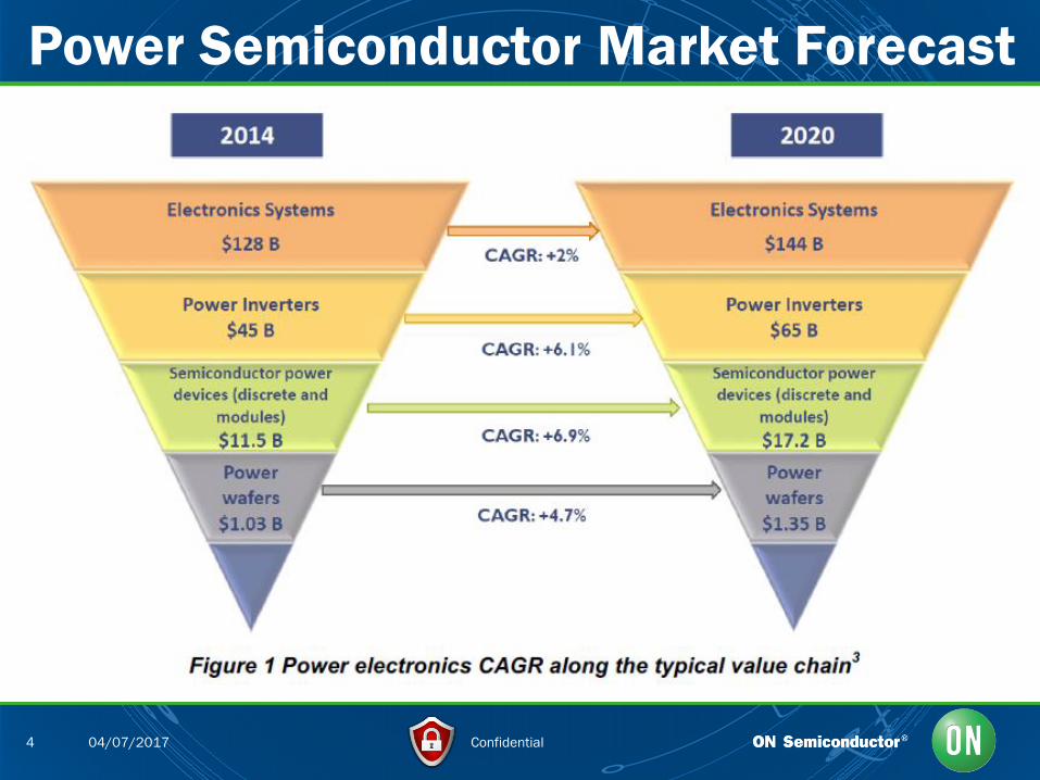
Power Semiconductor Market Forecast
Confidential 5 04/07/2017
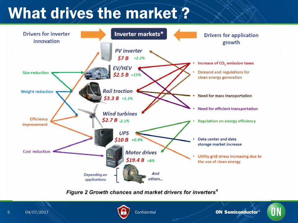
What drives the market ?

Confidential 6 04/07/2017
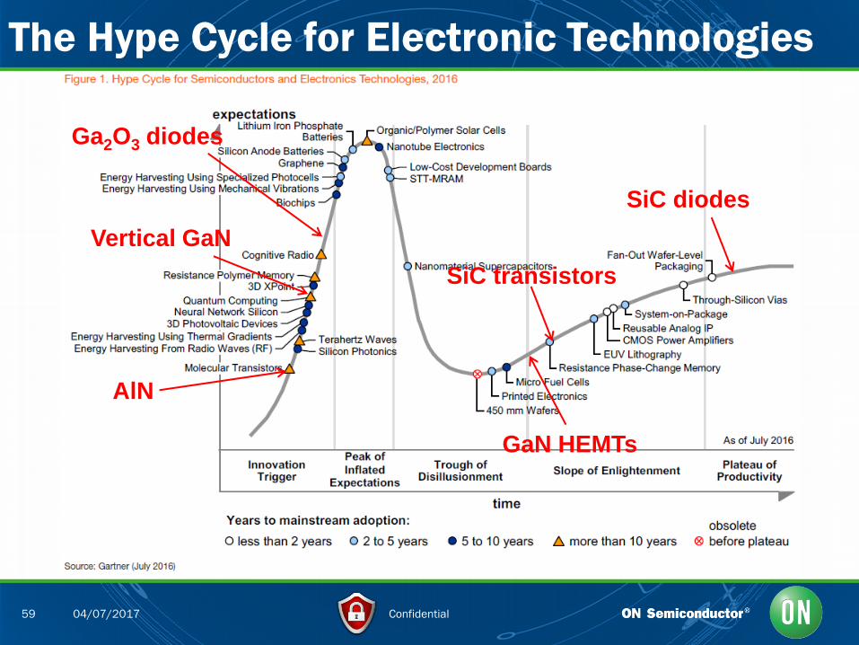
The Hype Cycle for Electronic Technologies
Confidential 7 04/07/2017
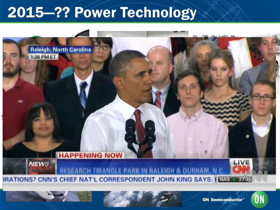
2015—?? Power Technology
Confidential 8 04/07/2017
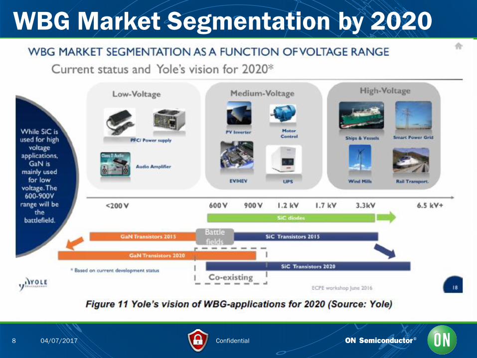
WBG Market Segmentation by 2020
Confidential 9 04/07/2017
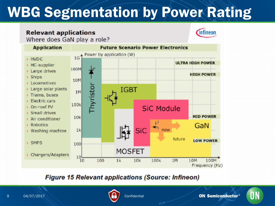
WBG Segmentation by Power Rating

Confidential 10 04/07/2017
WBG: High Potential for Market Disruption
Smaller Lighter
Cheaper Cooler
Stronger Greener Faster
~50% reduction in power loss
3-5x switching frequency
~15% system cost saving
One man installation
Cheaper maintainance
75% less weight
GaN Solution
Appliance Motor Drive System
Si Solution
170kg
0.41m3 30kg 0.09m3
SiC 1360 x 840 x 355 (840 x 355 x 1360mm)
840 x 787 x 254 (787 x 431 x 254mm)
*Illustrative representation
Solar Inverter
SiC Solution
Si Solution
Use of a 450 kW system
configuration realized with
hybrid SiCmodule, 28%
loss reduction
High Power Motor Drive System
Si Solution
SiC Solution
Laptop Power Supply
SiC Solution
Si Solution
Confidential 11 04/07/2017
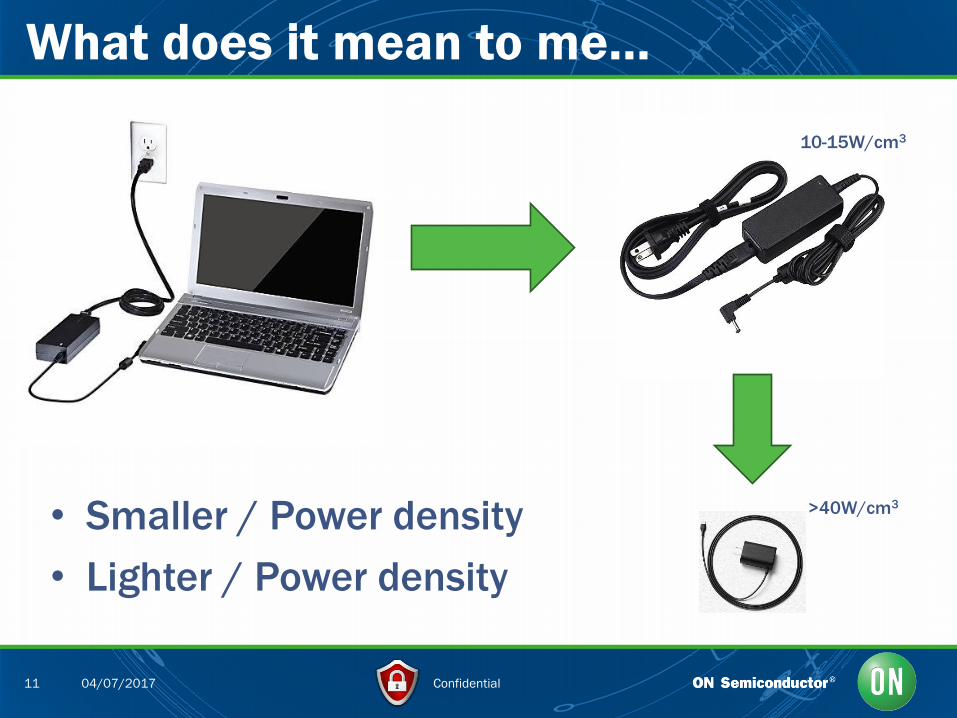
• Smaller / Power density
• Lighter / Power density
What does it mean to me…
10-15W/cm3
>40W/cm3

Confidential 12 04/07/2017
• https://www.gozolt.com/
Zolt Charger

Confidential 13 04/07/2017
• Lower electricity bill / Higher efficiency
• Fit it into the same space / Power density
What does it mean to me…
• 300M photos uploaded each day
• 300 hours uploaded every minute
• 10B hours watched per month
360,000 servers!
Annual maintenance cost ~200$/ft
150MW power usage/datacenter

Confidential 14 04/07/2017
• https://www.littleboxchallenge.com/
• Downscale a 2kW inverter down to the size of a tablet.
Google Little Box Challenge GaN
GaN SiC Target : P>50W/in3
Today : P~10W/in3
Winner : P=143W/in3
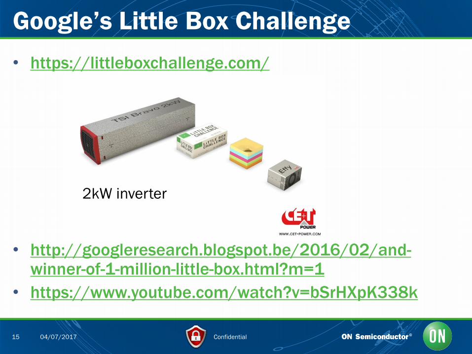
Confidential 15 04/07/2017
• https://littleboxchallenge.com/
• http://googleresearch.blogspot.be/2016/02/and-winner-of-1-million-little-box.html?m=1
• https://www.youtube.com/watch?v=bSrHXpK338k
Google’s Little Box Challenge
2kW inverter
Confidential 16 04/07/2017
• Power semiconductors are a hot topic
• Power devices=solid state physics
– 1D limit for a vertical transistor
– Resurf effect (2D)
• Non-polar and polar materials
– Concept of polarization charge
– Simple band structure
• HEMT “High Electron Mobility Transistor”
– Sheet resistance
– HEMT versus vertical power device
• Cost versus performance
Why are you here today ?
Confidential 17 04/07/2017
The ideal power semiconductor switch
• Off-state
– Should block a high voltage, with no leakage current
• On-state
– Should have no resistance (ideal conductor)
• During switching from off to on (and vice versa)
– Should happen immediately
– No hysteresis
– No charge storage
• Enabled by new material properties and novel device
concepts which enable new system solutions
Confidential 18 04/07/2017
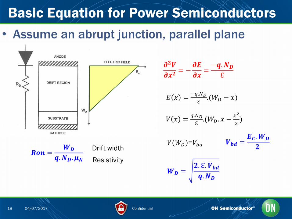
• Assume an abrupt junction, parallel plane
Basic Equation for Power Semiconductors
𝝏𝟐𝑽
𝝏𝒙𝟐 = −𝝏𝑬
𝝏𝒙=
−𝒒. 𝑵𝑫
ℇ
𝐸 𝑥 =−𝑞.𝑁𝐷
ℇ.(𝑊𝐷 − 𝑥)
𝑉 𝑥 =𝑞.𝑁𝐷
ℇ.(𝑊𝐷 . 𝑥 −
𝑥2
2)
𝑉(𝑊𝐷)=𝑉𝑏𝑑
𝑾𝑫 =𝟐. ℇ. 𝑽𝒃𝒅
𝒒. 𝑵𝑫
𝑹𝒐𝒏 =𝑾𝑫
𝒒. 𝑵𝑫. 𝝁𝑵
Drift width
Resistivity
𝑽𝒃𝒅 =𝑬𝑪. 𝑾𝑫
𝟐
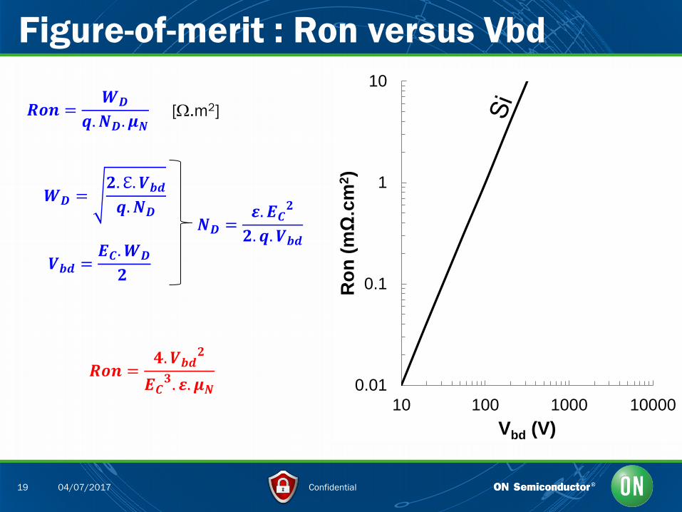
Confidential 19 04/07/2017
Figure-of-merit : Ron versus Vbd
𝑹𝒐𝒏 =𝑾𝑫
𝒒. 𝑵𝑫. 𝝁𝑵
𝑾𝑫 =𝟐. ℇ. 𝑽𝒃𝒅
𝒒. 𝑵𝑫
[.m2]
𝑽𝒃𝒅 =𝑬𝑪. 𝑾𝑫
𝟐
𝑵𝑫 =𝜺. 𝑬𝑪
𝟐
𝟐. 𝒒. 𝑽𝒃𝒅
𝑹𝒐𝒏 =𝟒. 𝑽𝒃𝒅
𝟐
𝑬𝑪𝟑. 𝜺. 𝝁𝑵
0.01
0.1
1
10
10 100 1000 10000
Ro
n (
mΩ.c
m2)
Vbd (V)
Confidential 20 04/07/2017
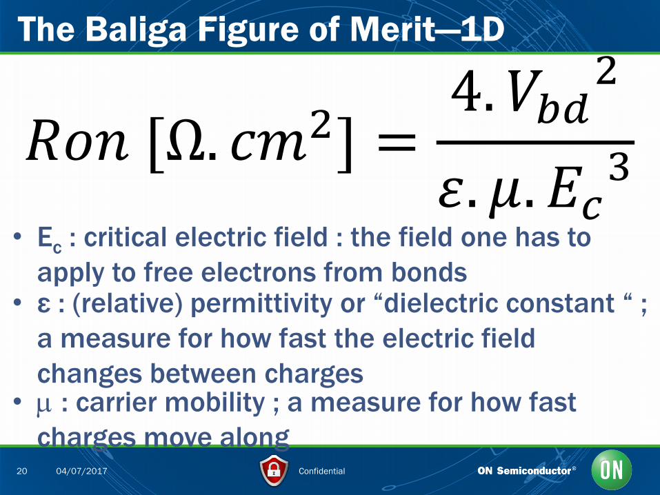
• Ec : critical electric field : the field one has to
apply to free electrons from bonds
The Baliga Figure of Merit—1D
𝑅𝑜𝑛 [Ω. 𝑐𝑚2] =4. 𝑉𝑏𝑑
2
𝜀. 𝜇. 𝐸𝑐3
• ε : (relative) permittivity or “dielectric constant “ ;
a measure for how fast the electric field
changes between charges • : carrier mobility ; a measure for how fast
charges move along
Confidential 21 04/07/2017
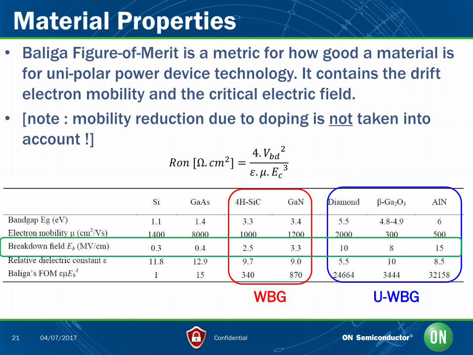
Material Properties • Baliga Figure-of-Merit is a metric for how good a material is
for uni-polar power device technology. It contains the drift
electron mobility and the critical electric field.
• [note : mobility reduction due to doping is not taken into
account !]
𝑅𝑜𝑛 [Ω. 𝑐𝑚2] =4. 𝑉𝑏𝑑
2
𝜀. 𝜇. 𝐸𝑐3
WBG U-WBG

Confidential 22 04/07/2017
Baliga FOM—only for drift region (1D)
𝑅𝑜𝑛 [Ω. 𝑐𝑚2] =4. 𝑉𝑏𝑑
2
𝜀. 𝜇. 𝐸𝑐3
S
D
Rcont
Rcont
Rchan
Rdrift
Rsubs
G
Confidential 23 04/07/2017
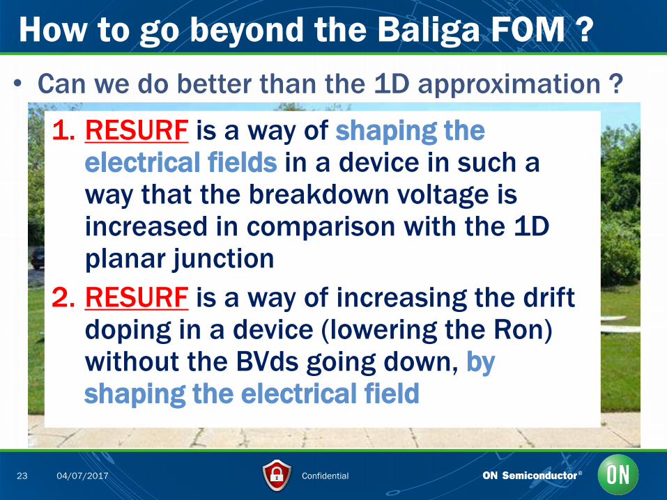
• Can we do better than the 1D approximation ?
How to go beyond the Baliga FOM ?
1. RESURF is a way of shaping the electrical fields in a device in such a way that the breakdown voltage is increased in comparison with the 1D planar junction
2. RESURF is a way of increasing the drift doping in a device (lowering the Ron) without the BVds going down, by shaping the electrical field
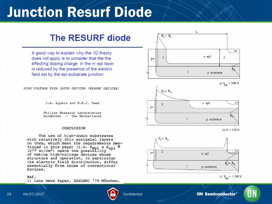
Confidential 24 04/07/2017
Junction Resurf Diode
Confidential 25 04/07/2017
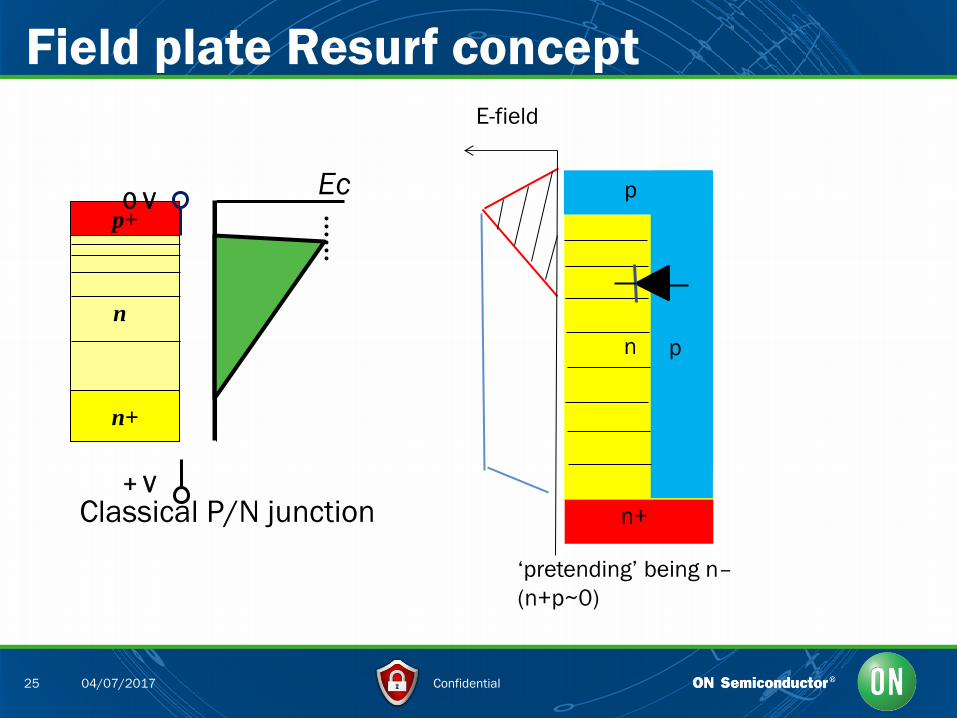
Field plate Resurf concept
n+
p+
n
Ec
Classical P/N junction + V
0 V
E-field
p
n+
n
‘pretending’ being n–
(n+p~0)
p

Confidential 26 04/07/2017
Volt Volt Volt Volt Volt
Super Junction Basics • The drift region is depleted from the side
instead from top-down. Full depletion
reached @ Vds~20-60V
GND
N+sub
N PP
N+sub
N PP

Confidential 27 04/07/2017
Resurf Limit (2D)—Optimal Charge 𝝏𝟐𝑽
𝝏𝒙𝟐= −
𝝏𝑬
𝝏𝒙=
−𝒒. 𝑵𝑫
ℇ
𝑅𝑜𝑛 =1
𝑞.𝑁𝑛.𝜇𝑁.
𝑝
𝑊𝑛.t
E-field
P+
n+
n p
Ec
Ec
Wn Wp
t
𝐸𝐶 =𝑞. 𝑁𝑛. 𝑊𝑛
𝜀𝑠+
𝑞. 𝑁𝑝. 𝑊𝑝
𝜀𝑠
𝐸𝐶 = 2.𝑞. 𝑁𝑛. 𝑊𝑛
𝜀𝑠
𝑁𝑛 = 𝑁𝑝 ; 𝑊𝑛 = 𝑊𝑝
𝐸𝐶 . 𝜀𝑠 = 2. 𝑞. 𝑁𝑛. 𝑊𝑛
𝑬𝑪. 𝜺𝒔 = 2. 𝑞. 𝑁𝑛. 𝑊𝑛 = 𝑸𝒐𝒑𝒕[𝐶
𝑐𝑚2]
Ec=[V]/[cm]
Eps=[F]/[cm]
[F]=[C]/[V]
Qopt (cm-2)
Si 1.96 1012
GaN 1.34 1013
SiC 1.64 1013
AlN 5.82 1013
Ga2O3 4.42 1013
𝑹𝒐𝒏 =𝟐. 𝒑. 𝒕
𝑸𝒐𝒑𝒕. 𝝁𝑵
𝑽𝒃𝒅 = 𝑬𝒄.t
𝑹𝒐𝒏 =𝟐. 𝒑. 𝑽𝒃𝒅
𝑬𝒄. 𝑸𝒐𝒑𝒕. 𝝁𝑵
𝑹𝒐𝒏 =𝟐. 𝒑. 𝑽𝒃𝒅
𝝁𝑵. 𝜺𝒔. 𝑬𝒄𝟐
p
Confidential 28 04/07/2017
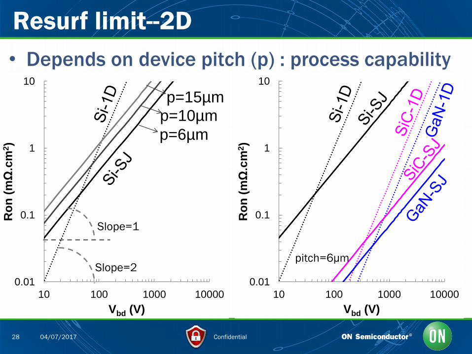
• Depends on device pitch (p) : process capability
Resurf limit--2D
0.01
0.1
1
10
10 100 1000 10000
Ro
n (
mΩ.c
m2)
Vbd (V)
p=6µm
p=10µm
p=15µm
0.01
0.1
1
10
10 100 1000 10000
Ro
n (
mΩ.c
m2)
Vbd (V)
pitch=6µm Slope=2
Slope=1
Confidential 29 04/07/2017
• Power semiconductors are a hot topic
• Power devices=solid state physics
– 1D limit for a vertical transistor
– Resurf effect (2D)
• Non-polar and polar materials
– Concept of polarization charge
– Simple band structure
• HEMT “High Electron Mobility Transistor”
– Sheet resistance
– HEMT versus vertical power device
• Cost versus performance
Why are you here today ?
Confidential 30 04/07/2017
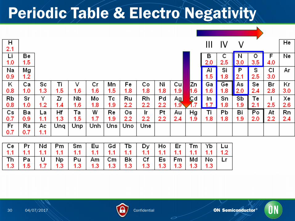
Periodic Table & Electro Negativity
III IV V
Confidential 31 04/07/2017
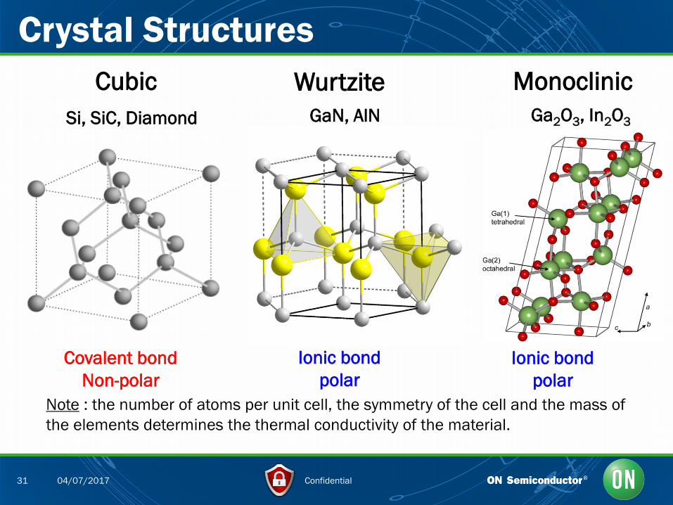
Crystal Structures
Si, SiC, Diamond GaN, AlN Ga2O3, In2O3
Cubic Wurtzite Monoclinic
Note : the number of atoms per unit cell, the symmetry of the cell and the mass of
the elements determines the thermal conductivity of the material.
Ionic bond
polar
Covalent bond
Non-polar
Ionic bond
polar
Confidential 32 04/07/2017
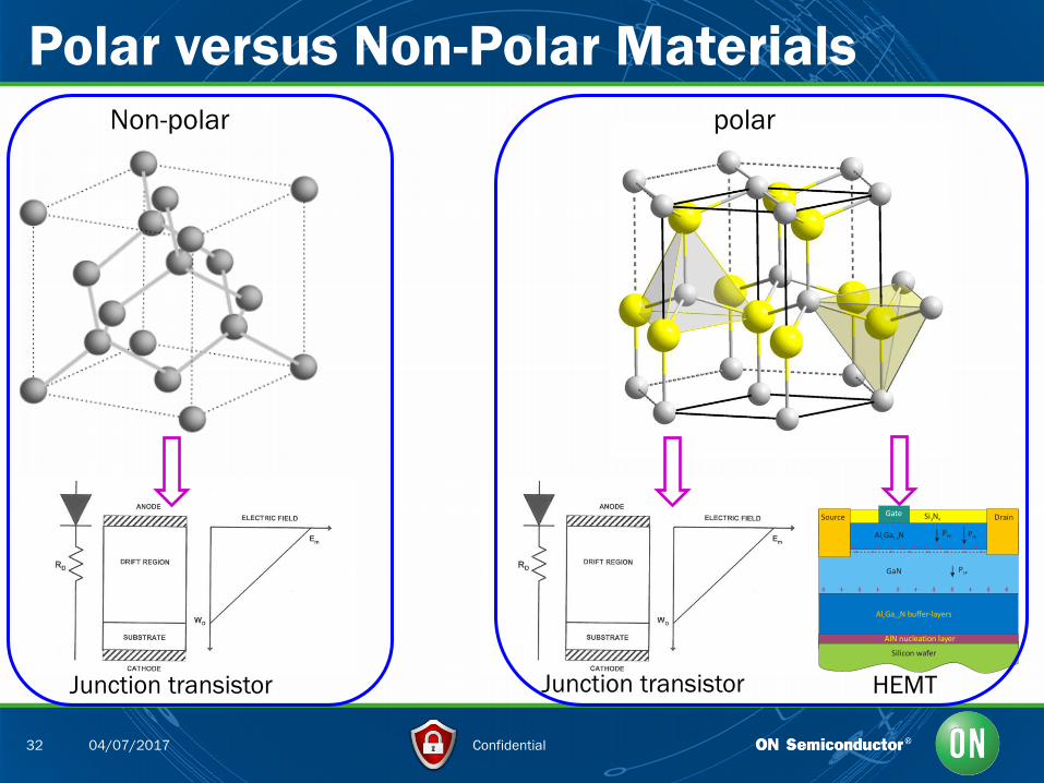
Polar versus Non-Polar Materials polar Non-polar
Source DrainGate
GaN
Al Ga Nx 1-x
PSP
PSPPPE
Si N3 4
Al Ga N buffer-layersx 1-x
Silicon wafer
AlN nucleation layer
Junction transistor Junction transistor HEMT
Confidential 33 04/07/2017
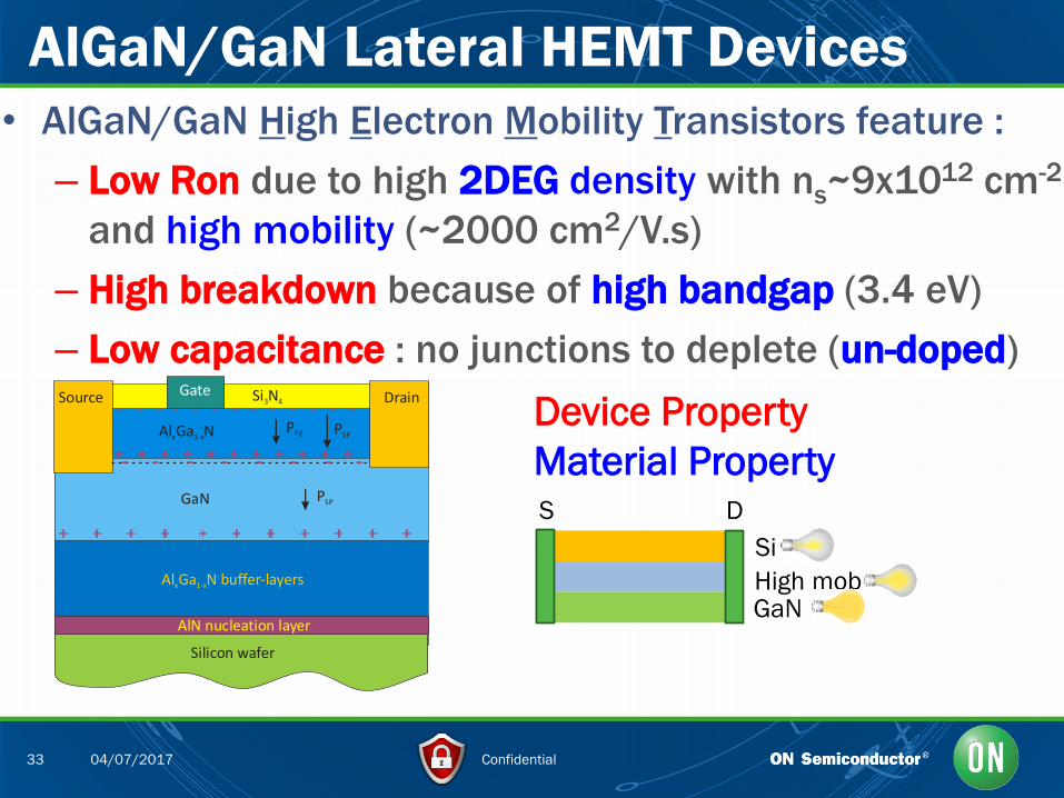
AlGaN/GaN Lateral HEMT Devices
• AlGaN/GaN High Electron Mobility Transistors feature :
– Low Ron due to high 2DEG density with ns~9x1012 cm-2
and high mobility (~2000 cm2/V.s)
– High breakdown because of high bandgap (3.4 eV)
– Low capacitance : no junctions to deplete (un-doped)
Si
High mob GaN
S D
Source DrainGate
GaN
Al Ga Nx 1-x
PSP
PSPPPE
Si N3 4
Al Ga N buffer-layersx 1-x
Silicon wafer
AlN nucleation layer
Device Property
Material Property
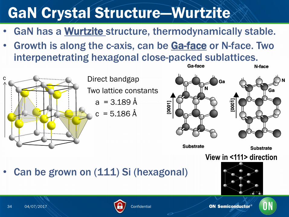
Confidential 34 04/07/2017
GaN Crystal Structure—Wurtzite • GaN has a Wurtzite structure, thermodynamically stable.
• Growth is along the c-axis, can be Ga-face or N-face. Two interpenetrating hexagonal close-packed sublattices.
• Can be grown on (111) Si (hexagonal)
View in <111> direction
Direct bandgap
Two lattice constants
a = 3.189 Å
c = 5.186 Å
c
Confidential 35 04/07/2017
Ga face
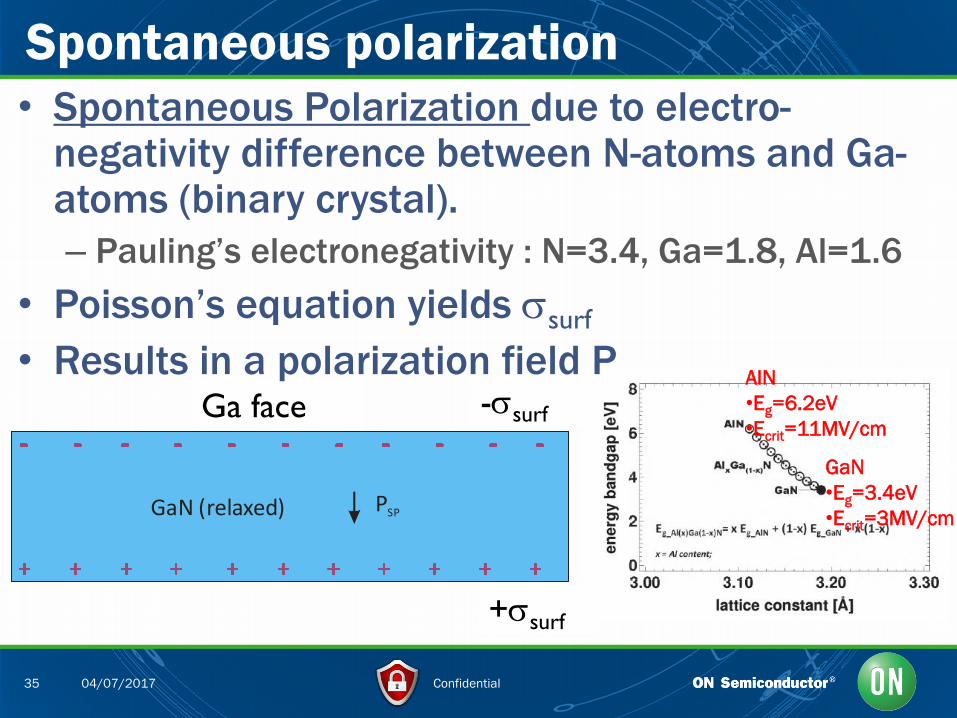
Spontaneous polarization
• Spontaneous Polarization due to electro-negativity difference between N-atoms and Ga-atoms (binary crystal).
– Pauling’s electronegativity : N=3.4, Ga=1.8, Al=1.6
• Poisson’s equation yields ssurf
• Results in a polarization field P AlN
•Eg=6.2eV
•Ecrit=11MV/cm
GaN
•Eg=3.4eV
•Ecrit=3MV/cm GaN (relaxed) PSP
-ssurf
+ssurf

Confidential 36 04/07/2017
sint
Spontaneous and piezo-electric polarization
GaN (relaxed)
Al Ga Nx 1-x
PSP
PSPPPE
• Al(Ga)N has larger polarization field than GaN
(due to larger Electro-negativity difference)
• Thin AlGaN layer strained piezo-electric pol.
• Induced net positive charge at the AlGaN/GaN
interface (but inside the AlGaN !) is very large !
– HEMT ns~ 1013 cm-2 Typical MOSFET ns ~1012 cm-2
Confidential 37 04/07/2017
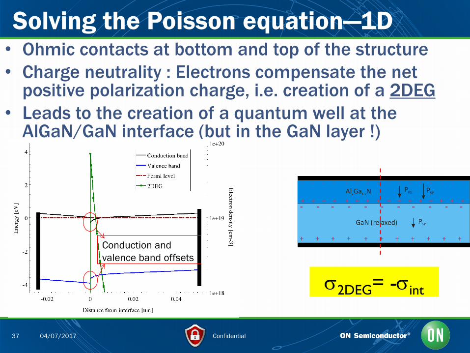
Solving the Poisson equation—1D • Ohmic contacts at bottom and top of the structure
• Charge neutrality : Electrons compensate the net positive polarization charge, i.e. creation of a 2DEG
• Leads to the creation of a quantum well at the AlGaN/GaN interface (but in the GaN layer !)
s2DEG= -sint
Conduction and
valence band offsets
Confidential 38 04/07/2017
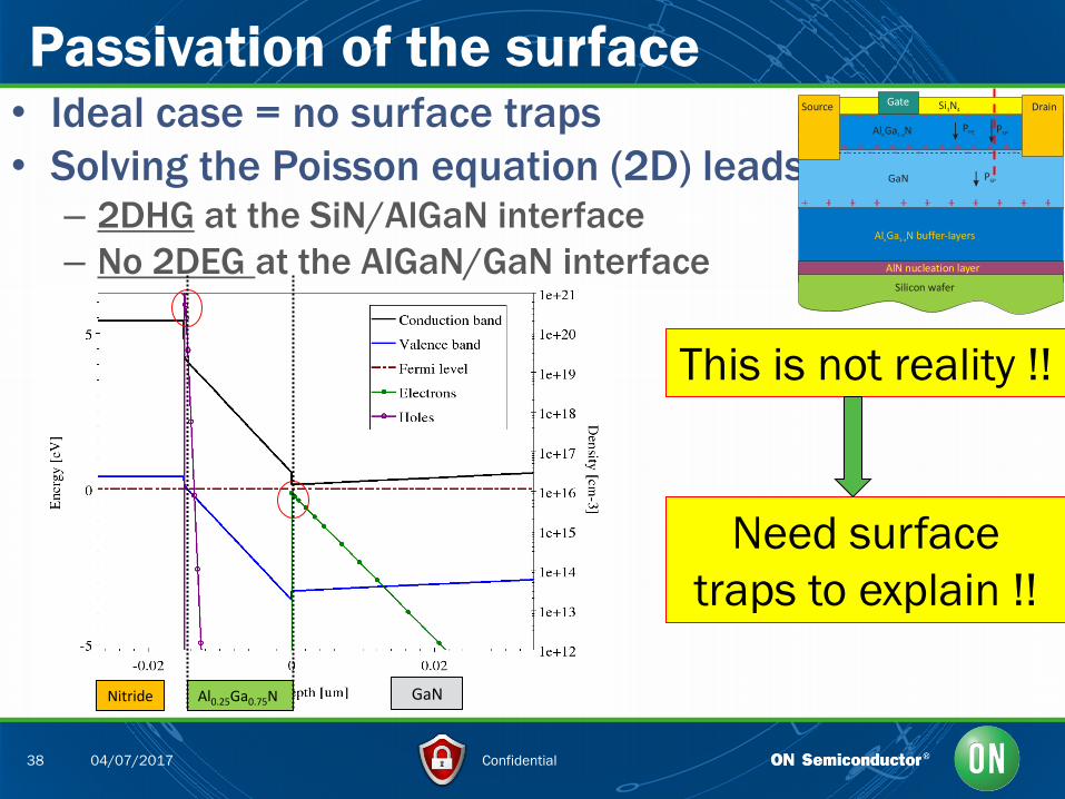
Passivation of the surface • Ideal case = no surface traps
• Solving the Poisson equation (2D) leads to : – 2DHG at the SiN/AlGaN interface
– No 2DEG at the AlGaN/GaN interface
Source DrainGate
GaN
Al Ga Nx 1-x
PSP
PSPPPE
Si N3 4
Al Ga N buffer-layersx 1-x
Silicon wafer
AlN nucleation layer
Al0.25Ga0.75N GaN Nitride
This is not reality !!
Need surface
traps to explain !!
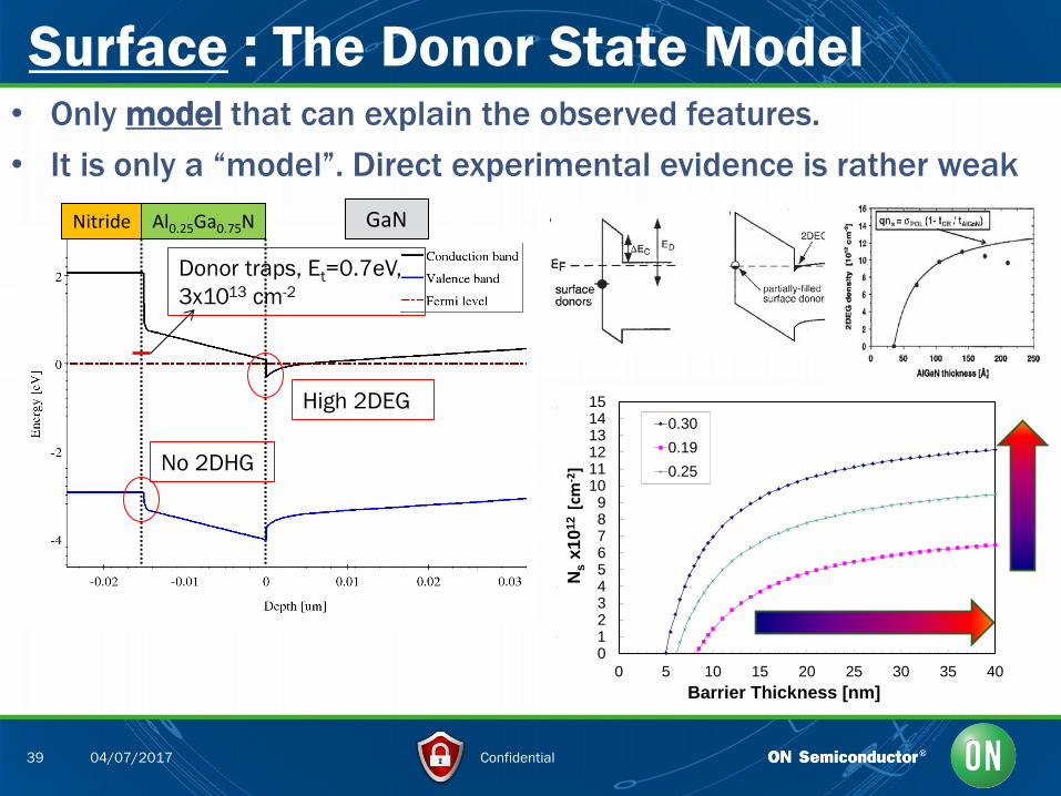
Confidential 39 04/07/2017
Surface : The Donor State Model • Only model that can explain the observed features.
• It is only a “model”. Direct experimental evidence is rather weak
Nitride Al0.25Ga0.75N GaN
Donor traps, Et=0.7eV,
3x1013 cm-2
No 2DHG
High 2DEG
• Donor type traps (neutral
when filled, positive when
empty), compensate for the
negative polarization charge
• A lot of charge (traps) !!
• Fermi level is pinned at the
donor trap level 0123456789
101112131415
0 5 10 15 20 25 30 35 40
Ns
x1
01
2 [c
m-2
]
Barrier Thickness [nm]
0.30
0.19
0.25
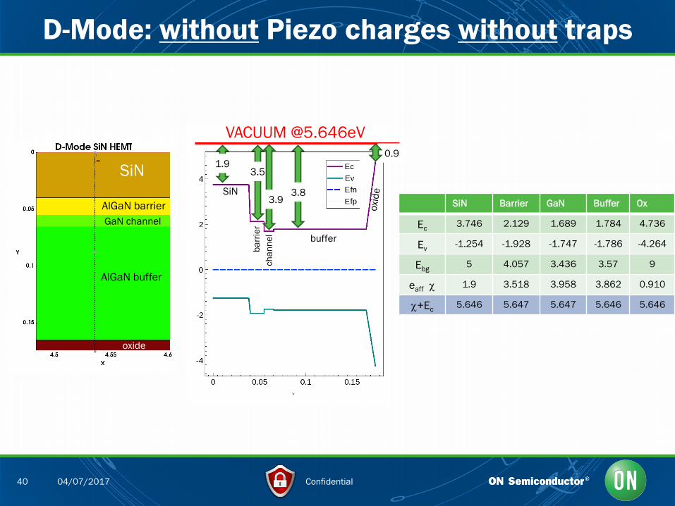
Confidential 40 04/07/2017
D-Mode: without Piezo charges without traps
SiN
ba
rrie
r
ch
an
ne
l
buffer
SiN Barrier GaN Buffer Ox
Ec 3.746 2.129 1.689 1.784 4.736
Ev -1.254 -1.928 -1.747 -1.786 -4.264
Ebg 5 4.057 3.436 3.57 9
eaff 1.9 3.518 3.958 3.862 0.910
+Ec 5.646 5.647 5.647 5.646 5.646
VACUUM @5.646eV
1.9 3.5
3.9 3.8
0.9
SiN
AlGaN barrier
GaN channel
AlGaN buffer
oxide

Confidential 41 04/07/2017
D-Mode: with/without Piezo charges without traps
SiN
AlGaN barrier
GaN channel
AlGaN buffer
oxide
SiN
ba
rrie
r ch
an
ne
l
buffer
- Pol charge
+ Pol charge +1.14e13 cm-2
-2.87e13 cm-2 (1)
(1) large neg. polar charge -2.87e13 cm-2 creates a h- gas at SiN/barrier interface
(2) Large pos. polar charge creates an e- gas at the buffer/oxide interface
- Pol charge -2.44e12 cm-2
+ Pol charge +1.97e13 cm-2 (2)
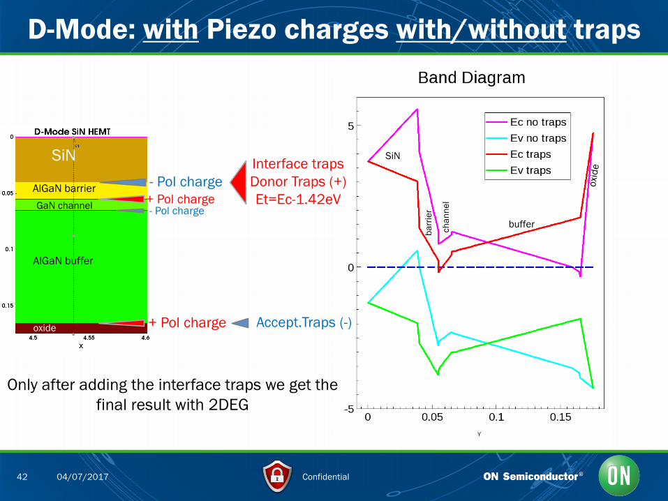
Confidential 42 04/07/2017
D-Mode: with Piezo charges with/without traps
SiN
AlGaN barrier
GaN channel
AlGaN buffer
oxide
SiN
ba
rrie
r
ch
an
ne
l
buffer
- Pol charge
+ Pol charge - Pol charge
+ Pol charge
Interface traps
Donor Traps (+)
Et=Ec-1.42eV
Accept.Traps (-)
Only after adding the interface traps we get the
final result with 2DEG
Confidential 43 04/07/2017
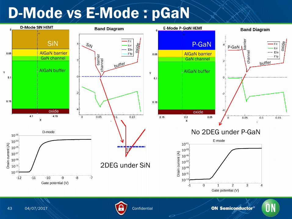
D-Mode vs E-Mode : pGaN
SiN
AlGaN barrier GaN channel
AlGaN buffer
oxide
P-GaN
AlGaN barrier GaN channel
AlGaN buffer
oxide
ba
rrie
r ch
an
ne
l
P-GaN ba
rrie
r ch
an
ne
l
No 2DEG under P-GaN
2DEG under SiN
- - - - - -
Confidential 44 04/07/2017
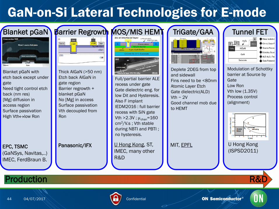
GaN-on-Si Lateral Technologies for E-mode
Blanket pGaN Barrier Regrowth MOS/MIS HEMT TriGate/GAA Tunnel FET
Blanket pGaN with
etch back except under
gate
Need tight control etch
back (nm res)
[Mg] diffusion in
access region
Surface passivation
High Vthlow Ron
Thick AlGaN (>50 nm)
Etch back AlGaN in
gate region
Barrier regrowth +
blanket pGaN
No [Mg] in access
Surface passivation
Vth decoupled from
Ron
EPC, TSMC
(GaNSys, Navitas,..)
IMEC, FerdBraun B.
Panasonic/IFX
Full/partial barrier ALE
recess under gate
Gate dielectric eng. for
low Dit and Hysteresis.
Also F implant
IEDM2016 : full barrier
recess with SiN gate
Vth >2.3V ; chan=160
cm2/V.s ; Vth stable
during NBTI and PBTI ;
no hysteresis.
U Hong Kong, ST,
IMEC, many other
R&D
Deplete 2DEG from top
and sidewall
Fins need to be <80nm
Atomic Layer Etch
Gate dielectric(ALD)
Vth ~ 2V
Good channel mob due
to HEMT
MIT, EPFL
Modulation of Schottky
barrier at Source by
Gate
Low Ron
Vth low (1.35V)
Process control
(alignment)
U Hong Kong
(ISPSD2011)
Production R&D
Confidential 45 04/07/2017
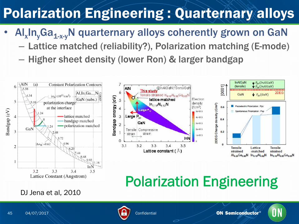
• AlxInyGa1-x-yN quarternary alloys coherently grown on GaN
– Lattice matched (reliability?), Polarization matching (E-mode)
– Higher sheet density (lower Ron) & larger bandgap
Polarization Engineering : Quarternary alloys
DJ Jena et al, 2010
Polarization Engineering
Confidential 46 04/07/2017
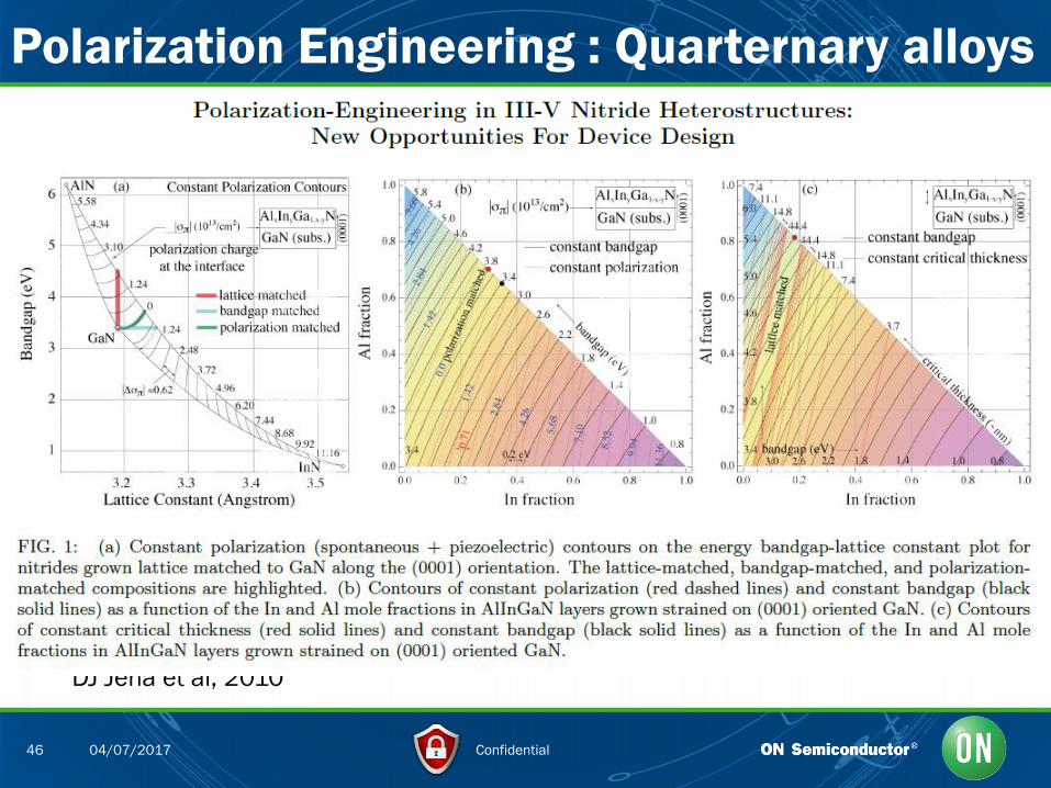
Polarization Engineering : Quarternary alloys
DJ Jena et al, 2010
Confidential 47 04/07/2017
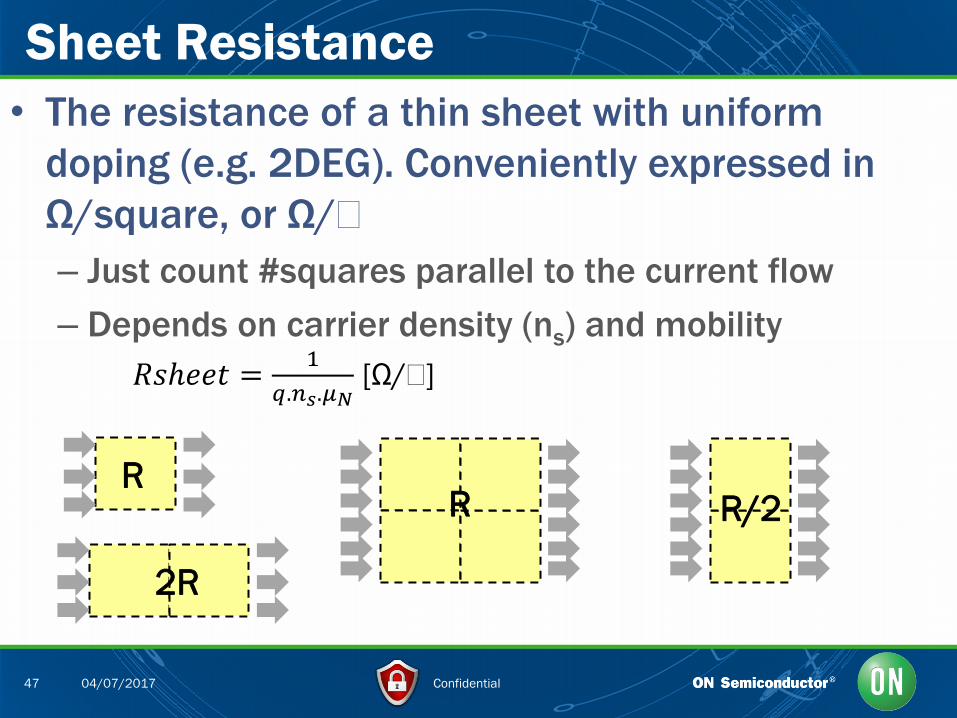
• The resistance of a thin sheet with uniform
doping (e.g. 2DEG). Conveniently expressed in
Ω/square, or Ω/
– Just count #squares parallel to the current flow
– Depends on carrier density (ns) and mobility
Sheet Resistance
R R
2R
R/2
𝑅𝑠ℎ𝑒𝑒𝑡 =1
𝑞.𝑛𝑠.𝜇𝑁 [Ω/]
Confidential 48 04/07/2017
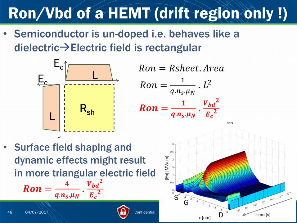
• Semiconductor is un-doped i.e. behaves like a
dielectricElectric field is rectangular
Ron/Vbd of a HEMT (drift region only !)
Rsh
Ec
Ec
L
L
𝑅𝑜𝑛 = 𝑅𝑠ℎ𝑒𝑒𝑡. 𝐴𝑟𝑒𝑎
𝑅𝑜𝑛 =1
𝑞.𝑛𝑠.𝜇𝑁 . 𝐿2
𝑹𝒐𝒏 =𝟏
𝒒.𝒏𝒔.𝝁𝑵 .
𝑽𝒃𝒅𝟐
𝑬𝒄𝟐
• Surface field shaping and
dynamic effects might result
in more triangular electric field
𝑹𝒐𝒏 =𝟒
𝒒.𝒏𝒔.𝝁𝑵 .
𝑽𝒃𝒅𝟐
𝑬𝒄𝟐
G S
D
Confidential 49 04/07/2017
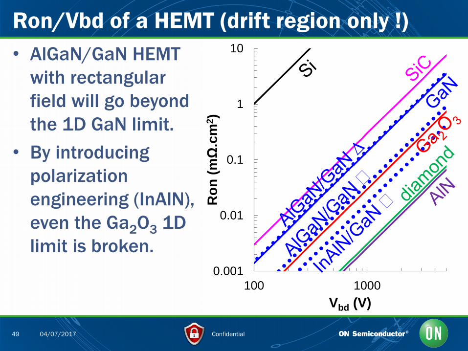
• AlGaN/GaN HEMT
with rectangular
field will go beyond
the 1D GaN limit.
• By introducing
polarization
engineering (InAlN),
even the Ga2O3 1D
limit is broken.
Ron/Vbd of a HEMT (drift region only !)
0.001
0.01
0.1
1
10
100 1000
Ro
n (
mΩ.c
m2)
Vbd (V)
Confidential 50 04/07/2017
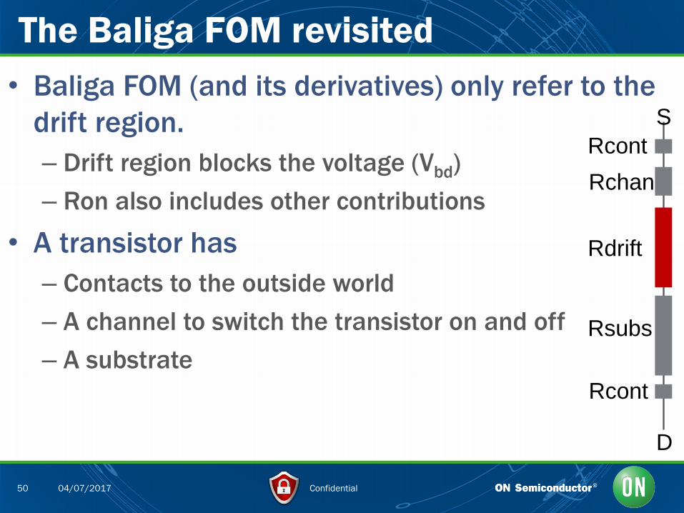
• Baliga FOM (and its derivatives) only refer to the
drift region.
– Drift region blocks the voltage (Vbd)
– Ron also includes other contributions
• A transistor has
– Contacts to the outside world
– A channel to switch the transistor on and off
– A substrate
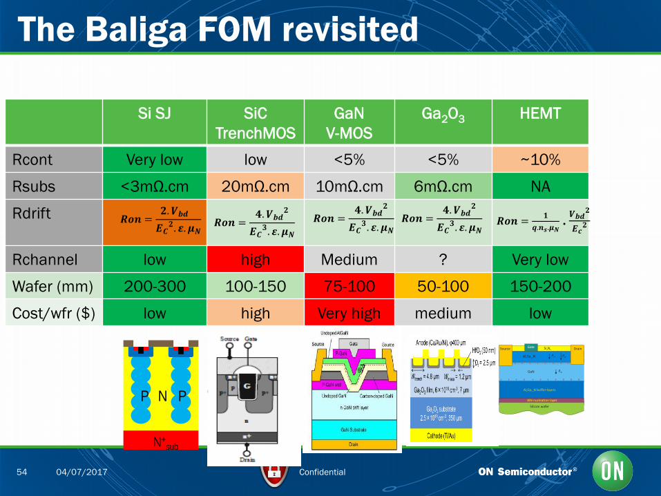
The Baliga FOM revisited
S
D
Rcont
Rcont
Rchan
Rdrift
Rsubs
Confidential 51 04/07/2017
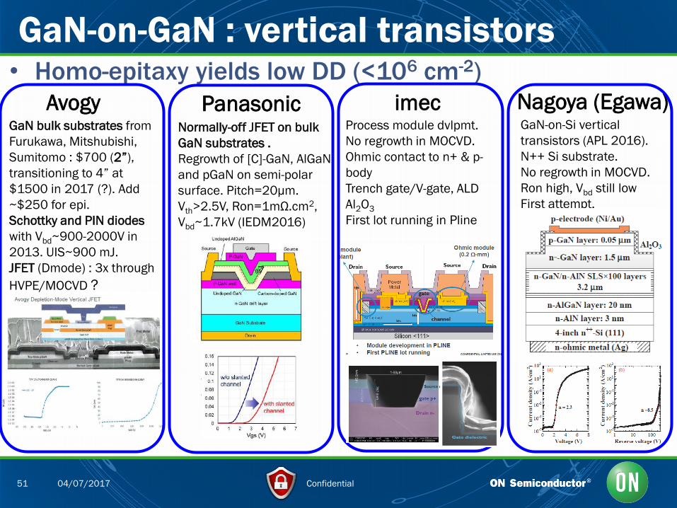
• Homo-epitaxy yields low DD (<106 cm-2)
GaN-on-GaN : vertical transistors
GaN bulk substrates from
Furukawa, Mitshubishi,
Sumitomo : $700 (2”),
transitioning to 4” at
$1500 in 2017 (?). Add
~$250 for epi.
Schottky and PIN diodes
with Vbd~900-2000V in
2013. UIS~900 mJ.
JFET (Dmode) : 3x through
HVPE/MOCVD ?
Process module dvlpmt.
No regrowth in MOCVD.
Ohmic contact to n+ & p-
body
Trench gate/V-gate, ALD
Al2O3
First lot running in Pline
GaN-on-Si vertical
transistors (APL 2016).
N++ Si substrate.
No regrowth in MOCVD.
Ron high, Vbd still low
First attempt.
Avogy imec Nagoya (Egawa) Panasonic Normally-off JFET on bulk
GaN substrates .
Regrowth of [C]-GaN, AlGaN
and pGaN on semi-polar
surface. Pitch=20µm.
Vth>2.5V, Ron=1mΩ.cm2,
Vbd~1.7kV (IEDM2016)
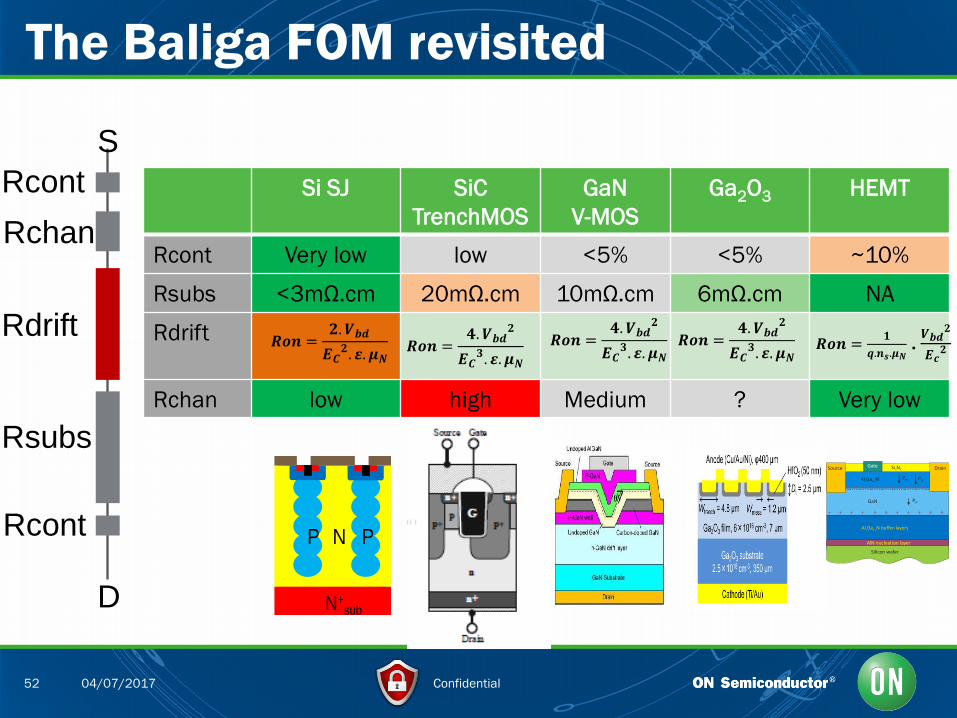
Confidential 52 04/07/2017
The Baliga FOM revisited
Si SJ SiC
TrenchMOS
GaN
V-MOS
Ga2O3 HEMT
Rcont Very low low <5% <5% ~10%
Rsubs <3mΩ.cm 20mΩ.cm 10mΩ.cm 6mΩ.cm NA
Rdrift
Rchan low high Medium ? Very low
𝑹𝒐𝒏 =𝟒. 𝑽𝒃𝒅
𝟐
𝑬𝑪𝟑. 𝜺. 𝝁𝑵
𝑹𝒐𝒏 =𝟐. 𝑽𝒃𝒅
𝑬𝑪𝟐. 𝜺. 𝝁𝑵
𝑹𝒐𝒏 =𝟏
𝒒.𝒏𝒔.𝝁𝑵 .
𝑽𝒃𝒅𝟐
𝑬𝒄𝟐 𝑹𝒐𝒏 =
𝟒. 𝑽𝒃𝒅𝟐
𝑬𝑪𝟑. 𝜺. 𝝁𝑵
𝑹𝒐𝒏 =𝟒. 𝑽𝒃𝒅
𝟐
𝑬𝑪𝟑. 𝜺. 𝝁𝑵
S
D
Rcont
Rcont
Rchan
Rdrift
Rsubs Source DrainGate
GaN
Al Ga Nx 1-x
PSP
PSPPPE
Si N3 4
Al Ga N buffer-layersx 1-x
Silicon wafer
AlN nucleation layer
N+sub
N PP
N+sub
N PP
N+sub
N PP
N+sub
N PP
N+sub
N PP
N+sub
N PP
Confidential 53 04/07/2017
• Power semiconductors are a hot topic
• Power devices=solid state physics
– 1D limit for a vertical transistor
– Resurf effect (2D)
• Non-polar and polar materials
– Concept of polarization charge
– Simple band structure
• HEMT “High Electron Mobility Transistor”
– Sheet resistance
– HEMT versus vertical power device
• Cost versus performance
Why are you here today ?
Confidential 54 04/07/2017
The Baliga FOM revisited
Si SJ SiC
TrenchMOS
GaN
V-MOS
Ga2O3 HEMT
Rcont Very low low <5% <5% ~10%
Rsubs <3mΩ.cm 20mΩ.cm 10mΩ.cm 6mΩ.cm NA
Rdrift
Rchannel low high Medium ? Very low
Wafer (mm) 200-300 100-150 75-100 50-100 150-200
Cost/wfr ($) low high Very high medium low
𝑹𝒐𝒏 =𝟒. 𝑽𝒃𝒅
𝟐
𝑬𝑪𝟑. 𝜺. 𝝁𝑵
𝑹𝒐𝒏 =𝟐. 𝑽𝒃𝒅
𝑬𝑪𝟐. 𝜺. 𝝁𝑵
𝑹𝒐𝒏 =𝟏
𝒒.𝒏𝒔.𝝁𝑵 .
𝑽𝒃𝒅𝟐
𝑬𝒄𝟐 𝑹𝒐𝒏 =
𝟒. 𝑽𝒃𝒅𝟐
𝑬𝑪𝟑. 𝜺. 𝝁𝑵
𝑹𝒐𝒏 =𝟒. 𝑽𝒃𝒅
𝟐
𝑬𝑪𝟑. 𝜺. 𝝁𝑵
Source DrainGate
GaN
Al Ga Nx 1-x
PSP
PSPPPE
Si N3 4
Al Ga N buffer-layersx 1-x
Silicon wafer
AlN nucleation layer
N+sub
N PP
N+sub
N PP

Confidential 55 04/07/2017
• Multiply Ron (mΩ.cm2) by cost/cm2
The Baliga FOM revisited—Cost
0.01
0.1
1
10
10 100 1000 10000
Ro
n (
mΩ.c
m2)
Vbd (V)
0.01
0.1
1
10
10 100 1000 10000
Ro
n.$
(mΩ.$
)
Vbd (V)

Confidential 56 04/07/2017
• Novel device concepts allow to go beyond the simple
1D FOM (resurf, superjunction)
• III-V materials are Polar (vs Si, which is non-polar).
• Most important (popular) III-V materials are :
– GaN, AlN, Ga2O3, In2O3
• Polar materials allow both junction transistors as
well as High Electron Mobility Transistors.
• HEMTs have lower Ron and lower Capacitance than
standard junction transistors in the same material.
• Don’t forget about cost ! Efficiency is key, but cost is
king !
Main Take-Aways
Confidential 57 04/07/2017
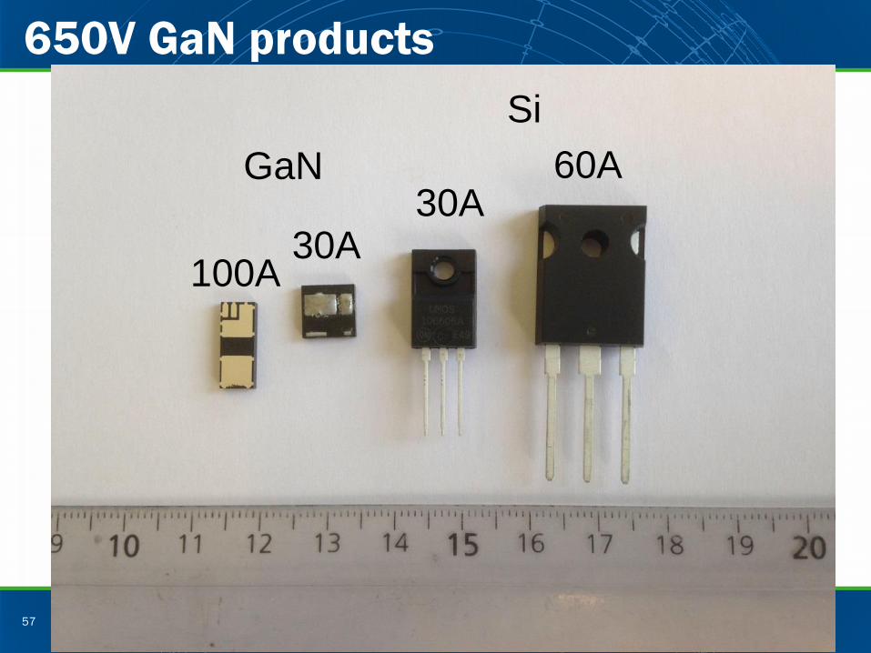
650V GaN products
30A 30A
60A
100A
GaN
Si

Confidential 58 04/07/2017
The end of the road for Silicon….
Is the start of the journey for WBG
Silicon
GaN
Ga2O3
AlN
Confidential 59 04/07/2017
The Hype Cycle for Electronic Technologies
SiC diodes
SiC transistors
GaN HEMTs
Vertical GaN
Ga2O3 diodes
AlN