free carrier absorption ehhlheeeeelii ok specialty
TRANSCRIPT

AD-A174 "5 DEVELOPMENT OF R FREE CARRIER ABSORPTION MEASUREMENT 1/2INSTRUMENT FOR INDTU (U) EAGLE-PICHER RESEARCH LABMIAMI OK SPECIALTY MATERIALS DIV 27 OCT 86
UNCLASSIFIED N88814-85-C-2418 F/G 28/12EhhlhEEEEEliIIIIIEEEEEIIIIIIEEEEEIIIIEEEIIEEEIIIEIIIIEE/E//I--nmE/EEEEEEEE-EgI/EIIhgEglEEEE/hE

'II" _IL25__
MICROCOPY RESOLUTION TEST CHART
NATIONAL BUREAU OF STANDARDS 1963-
DLI~~ I L14
la I
"MI
OZ 10 W
4m I4.

In to DTICLECTE
lot DECO03 SOBI
S D
Final ReportDevelopment of a Free Carrier
Absorption Measurement Instrument
ForIndium Phosphide and Gallium Arsenide
EAGLE PICHERR ES EA R CH L ABO0RA TO0R Y
This dOcx''Tn has ben approved5) afor p u b li : r i a .T d S IC its
di t1' ~ j,j jitod.
*Specialty Materials Division
86 11 6 052
o i P r
OTicS D L C T
DEC 0 3 ang
Final Report
Development of a Free Carrier
Absorption Measurement Instrument
ForIndium Phosphide and Gallium Arsenide
Contract No: N00014-85-C-2430
Prepared For: Naval Research Laboratory4555 Overlook Ave. S.W.Washington, D.C. 20375-5000
Prepared By: Eagle-Picher Research Laboratory200 9th Ave. N.E.Miami, OK 74354
v' cr~ ~pt~v Acesion ForEhis Ppro N IS CRA&I
fo ra 7 o7K d e ; itsILdi -CO01 Lt ; s unrirtfed.ICTA
- .announ'ced
27 October 1986..........
Availabilty Codes '
S Avail ar.d / or!'-Nb ist sptcilal

= laSPIOALTY MATMIALS DVIS11N UAOU.4ICR miAcHY
FEA FINAL REPORT
I. INTRODUCTION
This work represents an effort to develop and evaluate
a contactless method for determining the spatial variation
of the fr q-az econcentration in compound semiconductor
material he capab ility of performing such measurements
is of particular importance because of the current interest
in producing electronic grade wafers from the III-V and II-
VI compounds. These materials (particularly the II-VI
compounds) tend to be nonuniform due to preferential
migration of one of the constituents in the neighborhood of
growth defects. All semiconductors which are grown at some
finite temperature will contain Frenkel and Schottky point
defects; such defects in compounds tend to be of a
preferential nature which results in slight deviations from
stoichiometry. These deviations can result in significant
variations in doping concentrations and type. Defects in
the macrostructure such as twin lines, grain boundaries,
inclusions and dislocation lines can produce stoichiometric
gradations which will also result in doping variations
Utilizing traditional electrical characterization ethods on
such materials can be misleading. A HallsatuM re taken from
one portion of the wafer may yield re.-dIts which are not at
all descriptive of another portio or, of more concern, the
size of the Hall sample may prohibit a measure of the short
range variations which may exist throughout the material.I-he ability to distinguish short range variations in free
carrier concentration-,Q+--e an extremely valuable aid to
the crystal grower in the development of a particular growth
EA= t

SPICALTY MATMALS DIVISION EAGL.-PIIIR SMSASCH LAUORATO
Page 2
process -Ia- -Jar_, a contactless, rapid scanning probe
would permit a quick evaluation and should result in a more
direc and rapid evaluation of a particular crystal growth
sche 1e.
contactless method for measuring free carrier
conctntrations has been investigated at the Eagle Picher
Reseach Laboratory, Miami, Oklahoma. The basis for the
instrume is the free carrier absorption of infrared
radiation. Infrared absorption by free carriers in
semiconductors was-f!Z.t demonstrated by Fan and Becker
[1]. If this absorption property isto be exploited as a
measurement of free carrier concentration, there are a few
items which must be addressed taking into consideration that
the instrument will, in its simplest form, measure the
variation in an IR beam transmitted through the
semiconductor. These items for consideration include:
(1) a need to ascertain the absence of other
dominant absorption mechanisms at the frequency
(or band of frequencies) involved;
(2) establish a direct (preferably measurable)
relationship between the transmitted beam
intensity and the free carrier concentration;
(3) a better understanding of the impurity
concentration and degree of compensation can be
achieved through a knowledge of the dominate
scattering mechanisms;
(4) the material geometry, thickness, and
orientation, must be considered;
(5) the ultimate sensitivity and resolution must
determined.
% %

MSPALTY MATEIMALS IVISION EAGLI-PICHER RSEARCH LAORATORY
Page 3
One of the most attractive features of FEA in
semiconductors is that there is usually a band, 4<T<12um, in
which the free carrier absorption is the dominate
mechanism. Free carrier absorption is characterized by
monotonic spectrum which grows as Tp where p ranges from 1.5
to 3.5 and is determined by the dominate scattering
mechanisms. FEA characterization of semiconductors has been
preformed previously and of most significance to our effort
is the work of Jastrzebski, Lagowski and Gatos [2) which
involved the use of a scanning CO2 laser to obtain spatial
resolution of the impurity concentrations in silicon.
Boone, Cantwell and Shaw [3) have demonstrated the
practicability of using a scanning CO2 laser for
mapping CdS wafers; the work reported here is an extension
of that effort which has the objective of demonstrating the
feasibility of developing an FEA instrument which can
provide an automated, rapid scan of a semiconductor wafer.
Further, the measurement is contactless with no wafer
preparation such as an antireflective coating.
E QLE PKHM
-~~~~~A fI ' % *-'-Z *y.L

S-IALTY MATEIALS DIVISOd EAGLU.4CHI MS MAMcH LASOAWORV
SPage 4
II. THEORETICAL DISCUSSION
The operation of this FEA instrument is based upon the
absorption of a CO2 beam propagating through a semiconductor
wafer. According to classical electromagnetic theory [4] a
coherent plane wave normally incident upon a lossy
dielectric slab has a transmission coefficient given by
[(l-R1 2)2 + 4R12 Sin2612]exp(-cd)
(1) T =_____________ __
[l-R 1 2 exp(- d) ] 2 + 4R 12 Sin 2 (612 +K2 d)exp(-od)
where
(K1 - K 2 ) 2 + (ot/2) 2
I1(2) = 2
(K1 + K2) + (c/2)
Iand
(3) 6 = Tan-l[-K */(KI2 - K 2 + (/2) 2M.A12 Ta (K/K 1 2 H
Where % is the absorption coefficient which is related to
the complex conductivity (c') by the expression
= €' (s/E) K and K are the propagation constants forv2 1the semiconductor and free space, respectively, given by
= (r) and K 1 = W(Po(o) where w is the frequencyK2 W( o()ad
(radians/sec), d is the wafer thickness (cm), Po is the
free space permeability, ( is the free space permittivity,°0u is the semiconductor permeability and ( is the
semiconductor permittivity.
RE t EPNIM
" U ini i Ii J .. " .. '

SIICALTY MATIlALS DIVISION UAOJ-PICHEE ISIAOIC LAWRATORY
Page 5
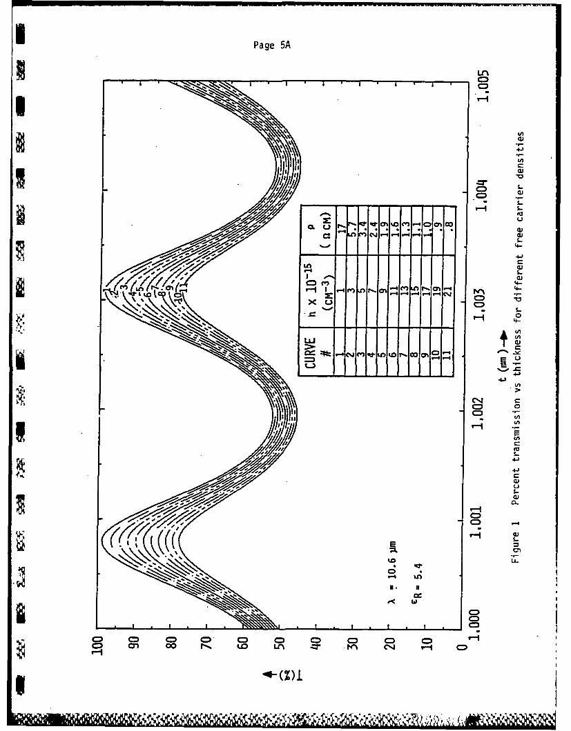
Equation (1) indicates that the transmission is
critically dependent upon the path length through the
semiconductor. Figure 1 is a computer generated curve
showing T (%) versus wafer thickness for T=10.6um and
( =5.4. This figure clearly shows that for thicknessr
variations of the order of lum, the transmission coefficient
can change by 10% to 15% which would match the variations
due to free electron absorption. This large variation is
the result of wave interactions which are dependent upon the
spacing, in wavelengths, between the two air/dielectric
interfaces. By adjusting the path length between the two
surfaces of the wafer one can maximize the transmission
coefficient such that
(1-R12 ) 2exp(-(d)
(4) Tmax [l-R 1 2 exp(-o(d) ]2
where it has been assumed that 6 2zO. Now the fractional
change in Tmax can be expressed as
-[I + R 2exp(- od)] A (od)
(5) ATmax /Tmax =(1 -R 12 exp(-ord)]
and A(o(d) = orAd + dAN. Thus, one must now evaluate the
relative changes in the absorption coefficient (o) as
opposed to the wafer thickness (d). If or is simply
proportional to n then A(od) can be expressed as
(6) (Aod)/ord = Ad/d + An/n
EMLE 9bI WHR
%. ~ . r
Page 5A
U Ln
C)~
CD
~0)4--
%- 4-
V-4 S-
x CD
'4
.. ~ '-14-)
S- 4-)
CD
V- U';
C)C
a)t

SPICIALTY MATERIALS DIVISION PAGLE-PICHEE RESEARCH LABOATORY
Page 6
which implies that if the objective is to measure An then
the condition that An/n >> Ad/d should be maintained. This
could place a
constraint on the sensitivity. For example if Ad=lum, d=lmm
and the nominal value for n is 10 1 5cm 3 . Then to ascertain
that the measurement is indicating a variation in free
carrier density, one must consider only those deviations
such that
(7) An >> nAd/d= l02cm .
Of course, this is a 0.1% variation and should
represent adequate sensitivity for most measurements.
However, the theoretical sensitivity can be significantly
improved if the overall thickness variation is held to less
than one wavelength (z3um). Since the Ad represents a
variation in the path length, the obvious way to avoid
thickness limitations on sensitivity is to keep d constant.
Figure 2 represents a wafer with thickness variations.
dma x
Figure 2: Wafer thickness variations; dmax -dmin +
If d i dmax + T then the beam path length can bemaxheld constant by adjusting the angle of incidence such that
the path length is constant; further, if the path length is
E L,°.

SPECIALTY MATMALS DIVISION BAOU-PICHER RSUASCH LADOATOSY
*Page 7
adjusted to an integer number of wavelengths, the maximum
sensitivity will be achieved as described by equation (5).
Thus, the smallest angle, Oimin' for which the transmission
maximum occurs is determined such that
(8) d Cos(O..) = d with d = mT and m
1,2,3,4,5 .....
then it must be ascertained that
(9) (d min)/Cos( imax) = mT
this is to insure that the path length stays at d=mr and not
(m±p)T where p=1,2 ,3 .... The simplest way to insure that
equation (9) holds is to make certain that dmax - dmin i T
which is not a stringent requirement. The actual
measurement technique involves rotating the sample through a
small angle seeking the transmission maximum nearest 0 =0.
Theoretically, the relation between transmission variations
and the absorption coefficient becomes
(1 + Rl 2 exp (-ocd) } ((d) (Aic/x)
(10) ATmax /Tmax
ai (1 - R1 2 exp(-xd))
In this instance, the absorption coefficient,N, is a measure
of the attenuation of the infrared beam due to the free
electron interactions with incident photons. The photon
absorption by the free electrons is a two step process which
includes electron-phonon interaction as a necessity for the
conservation of momentum. Lattice vibrations, impurities
ESOLE PIHER
.U

$PICALTY MATEIALS DIVISION EAGUJ-PICHE RESIARCH LABORATORY
Page 8
and lattice defects (acting as scattering centers for free
electrons) give rise to absorption. These scattering
processes result in small energy variations such that
secondary perturbation theory [5] can be used to determine
the transition probability for each of the scattering
processes. For semiconductors, there are five scattering
mechanisms which may be significant depending upon the
crystal structure, defects and impurity concentrations.
These mechanisms are acoustic phonon, optical phonon, polar
optical phonon, piezoelectric and charged impurity
scattering. Ridley [5] among others has developed the
theoretical expressions for these scattering mechanisms. Of
particular significance to this work is the functional
dependence of absorption coefficient (o) upon the free
electron density and wavelength of the incident radiation.
In the wavelength range of free carrier absorption, N can be
expressed approximately as a sum of the absorption
coefficients due to various scattering process, for most
cases of interest (at room temperature),
op1 'r = 2.5 + 0 .im T3.5 + (x acT1.5 + cc pzT2.5op Imp ac pz
where the terms on the right hand side represent the
contributions form optical phonons, ionized impurities,
acoustical phonons and piezoelectric contributions
respectively. The coefficients m 0( and (p are all
linear in n while 0imp is proportional to the product NI n
where NI is the concentration of ionized impurities. Thus,
for an uncompensated semiconductor, a is proportional to
n2 . In principle, it should be possible to determine the
degree of compensation in a doped semiconductor by observing
EAGLE @j) IEIMEMl lCHE
'p ~

SPECIALTY MATERIALS DIVISION EAGLE-PICHER RESEARCH LABORATORY
Page 9
the dependence of the coefficient N. on the free electronimp
concentration. This will require the introduction of the
temperature as a variable as a means to incorporate
variations in n into the measurements. Obviously, it is
possible to isolate on various scattering mechanisms by
operating over specific temperatures ranges. All of our
work performed to date has been done at room temperature
although we have conducted extensive studies on the
temperature dependence of mobility and free carrier
concentrations using conventional measurement techniques
[6].
From equation 11 and the equation for the transmission *4
coefficient it is possible to determine the dominate
scattering mechanism (if one exists) on the basis of the
wavelength dependence of the scattering terms. For most
semiconductors at room temperature, piezoelectric scattering
is not a significant factor so that each of the common
scattering mechanisms has a different wavelength
dependence. If an incoherent source such as a scanning IR
spectrophotometer is employed;
2 '(12) T = (1 -R 12 exp (-2 cd)
1-12
For the values of R12 and Nd normally encountered
12%
(13) Ln(T) z 2Ln(l - R 1 2) - cd
FAE Ob PIC HER
J.

SPECIALTY MATERIALS DIVISION EAGL-PICE RUSRUARCH LAOEATORY
Page 10
and
(14) Ln[Ln(T) - 2 Ln(l - R12)] = Ln(op ) + 2.5 Ln(T)
+ Ln(o( imp ) + 3.5 Ln(T) + Ln(ac ) + 1.5 Ln(T)
+ Ln(d) = Ln(Cd)
therefore, a plot of Ln(Cd) vs Ln(T) will yield a slope
which is characteristic of the scattering process [3]. If
the dominate scattering processes are unknown, this
procedure should be employed as a basis for the scanning IR
_ measurements.
If it is determined that the dominate scattering is
impurity scattering then the relation between the absorption
coefficient and free electron concentration must be
established. Obviously if
(15) ocd = A(T,T)n k lI K ( 2
a plot of Ln(od) vs Ln(n) should yield a slope of K which is
indicative of the degree of compensation. One approach is
to make successive measurements at a constant wavelength at
different temperatures; it is possible to calculate the
changes in free electron concentration since it is known
that
(16) n - Nc exp[-(E c - Ef)/KT]
k for nondegenerate semiconductors. However, the temperature
dependence of the scattering process must be known and taken
into consideration when interpreting the data. This report
SAM, I iPKHR

SPIIALTI MATIALS DIVISION EAGLE-.PtOI 1SAR04 LASORATORY
Page 11
does not encompass any temperature variations in the FEA
measurements; it would appear that such measurements would
enhance the value of the FEA instrument.
Returning to equation (10), if ad is assigned an
average value, a d; then we can write
-El + R1 2 exp(-o(0d)](a 0d)(A/ o )
(17) ATmax /Tomax =(1 - R12 exp(- 0 d)]
where Tomax corresponds to a 0d. If a = AnkiP the ratio
Aa/0 can be written as,0
(18) Aa/c ° = K(An/n0 )
where K=2 for uncompensated impurity scattering and K=1
otherwise; of course, an effective K between 1 and 2 can be
determined for a combination of scattering processes which
includes ionized impurities. Generally at room temperature
taking a value of K=l will not produce serious error. Since
the primary objective of this work has been to explore the
limitations on sensitivity and resolution, we have taken the
bulk Hall reading from a designated area to establish n and
have taken an average Tmax over that region to establishT omax'
If equation (17) is used to describe the relationbetween the transmission coefficient and the free carrier
variations, it is apparent that fractional changes have a
near linear relationship. Of course 0 d is directly
tf
EMLE~ 9bD r\4 N
SPICALTV MATIIALS DIVISIH ,AOU-ICH-2 RISIA LABOATORY
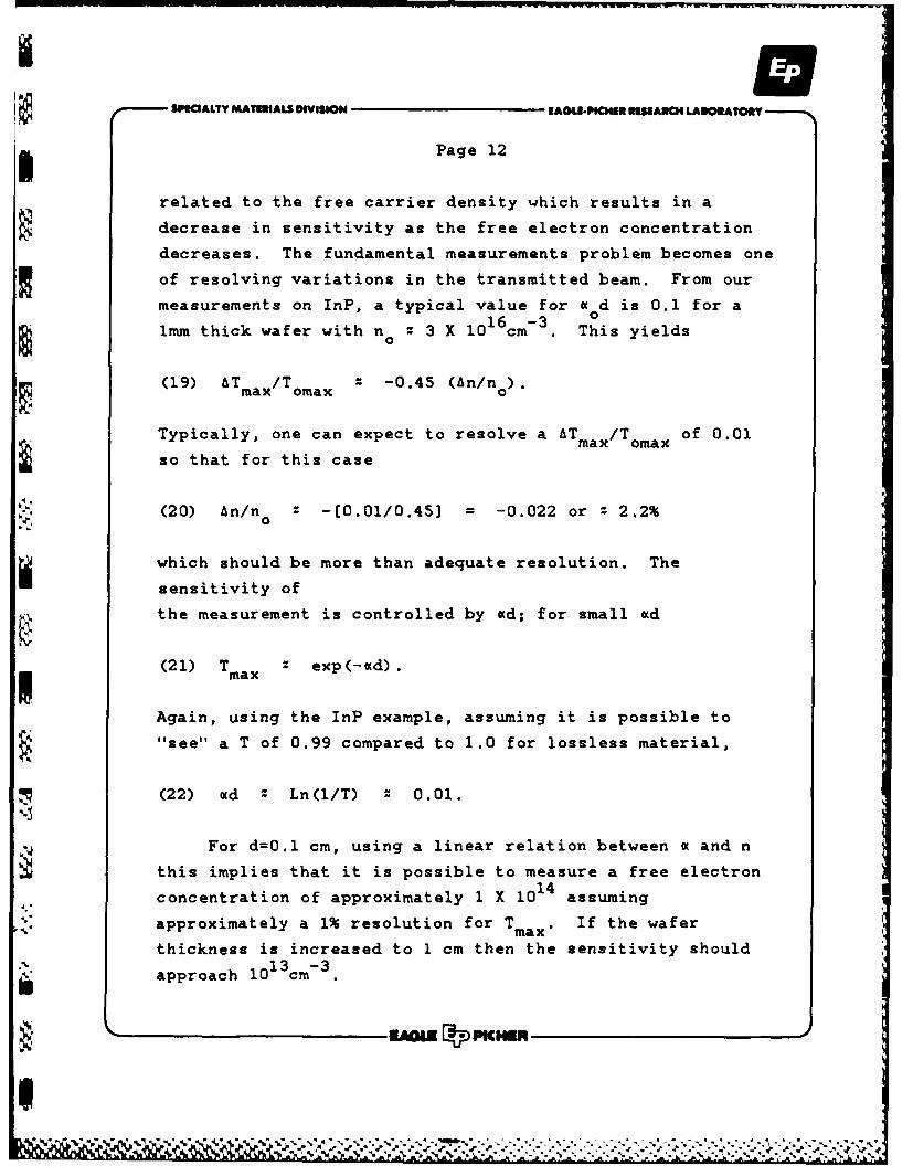
3 Page 12
related to the free carrier density which results in a
decrease in sensitivity as the free electron concentration
decreases. The fundamental measurements problem becomes one
of resolving variations in the transmitted beam. From our
measurements on InP, a typical value for a 0d is 0.1 for a
1mm thick wafer with n0 z 3 X lO 6cm 3 . This yields
(19) AT max/Tomax Z -0.45 (An/n ).
Typically, one can expect to resolve a ATmax/Tomax of 0.01
so that for this case
(20) An/n 0 z -(0.01/0.45] = -0.022 or z 2.2%
which should be more than adequate resolution. The
sensitivity of
the measurement is controlled by od; for small kd
(21) Tmax exp(-od).
Again, using the InP example, assuming it is possible to"see" a T of 0.99 compared to 1.0 for lossless material,
(22) o d =Ln(I/T) z 0.01.
For d=0.l cm, using a linear relation between o and n
this implies that it is possible to measure a free electron
concentration of approximately 1 X 10¹⁴ assuming
approximately a 1% resolution for Tmax . If the wafer
thickness is increased to 1 cm then the sensitivity should13 -3approach 10 cm
_ ME E!PWNE
-i SPICALTY MA111LS DIVISION RALbOE4-M URSIAiCH LAOWRATORY
Page 13
The ultimate resolution of the transmission
coefficient is controlled by the system; some sources of
system "noise* are:
(1) variations in the laser power level due to
temperature variation, mode hopping or discharge
current instability
(2) variations in the channel transmission
characteristics due to temperature variations in
material properties; this includes the air portion
of the channels
(3) fluctuations in the IR detector response due
*t to thermal or mechanical variations
(4) stray IR radiation entering the system from
outside sources
(5) and, in our system, instabilities in the
rotary platform due to mechanical vibration.
The ultimate sensitivity of the system is limited by
the ability to resolve small changes in the transmission
coefficient which are the result of changes in the
absorption. To detect free electron densities less than
101 3 cm- 3 will require careful design of the system to
minimize the sources of noise described above.
I
!MI MCMM
p11

SPICALTY MATIEALS NVSION EAGLUI-PIHIF=AJ IC LA@CeAOSroV
Page 14
III. THE FEA SYSTEM
IIIA. SYSTEM DESCRIPTION
The system uses a beam splitter made of CdTe to split
an incident CO2 laser beam into a reflected beam for
reference beam intensity information and a transmitted beam
for probing the sample.
The sample beam is focused using a germanium lens of
very short focal length through a pinhole which eliminates
any laser speckle that may cause intensity changes across
the sample beam. The sample beam is then diffraction-
limited by the pinhole size such that the beam diameter is
uniform over approximately a one-inch diameter at the sample
position. The incoming laser beam is attenuated with a
germanium or silicon absorber to a level that will not
overdrive the lithium tantalate detectors. The incoming
laser beam is also chopped at a frequency of near 200 hertz
to provide a pulsed beam for signal processing. The output
of the chopper signal is used to trigger a Lock-In Amplifier
(LIA). One LIA is used on the reference beam and a
different LIA is used to detect the 10.6-micron transmission
through a sample.
The sample is mounted on an X,Y,Z,THETA(Y) stage which
allows both peaking and mapping of the sample. For each
sample the incident face of the sample crystal is placed on
the Y-axis using the Z-translation stage. The sample isathen brought to the first maximum transmission to the leftNO fM

SPICALTY MATIALS DIVISON AOU.PIC IMrERASCH LANORATO@Y
Page 15
or right of center using the THETA(Y) rotation. The
transmitted 10.6 micron radiation is reflected from the face
of a metallized 450 prism through the detector aperture onto
the detector.
The sample is mapped using the X,Y translators for each
X,Y coordinate. The resolution of the translators is 10-
microns, but for this work the resolution was limited by the
detector aperture which was 0.037-inches or 940-microns.
The beam-splitter/reference detector module was
machined from aluminum and has parallel machined slots at450 for one, two, or three beam splitters as well as a
detector mount and multiple beam attenuator holders. The
module also has large circular apertures to limit the amount
of beam scatter arriving at the reference detector and the
ji sample detector.
The sample beam from the beam-splitter is focused with
a short-focal-length germanium lens (2.1-cm.) onto a pinhole
(0.037-inch diameter) machined into a piece of brass
shimstock. The spatial filter action of this arrangement
decreases beam wonder and the speckle normally associated
with laser beams. The housing and lens holder for the
spatial filter were machined from aluminum. The germanium
lens is secured by a threaded end cap and the pinhole is
movable in a slot and secured by two cap screws at the focal
length of the germanium lens.
The prism/sample-beam-detector module was machined from
aluminum. It consists of a level platform and milled slot
I,. for the prism and its translator, and a detector holder and
slot for the detector aperture. The prism can be translated
in the Z-direction to pick off the sample beam at different
' " -A= ItD PIKER

SPICALTY MATEIIALS DVISION EALE-PICHER RESEARCH LAORATOeT
Page 16
spots along the X-axis. The Lithium tantalate detector has
an active diameter of 1.25-millimeters and the detector
aperture limits the size of the sample beam on the sample to
the aperture size.
The CO2 laser is a Line Lite Laser Model #950
continuous laser with piezostack wavelength selection. The
laser is water cooled with a closed system
refrigerator/heater heat exchanger and pump system. The
output at 10.6-microns is nominally 8-watts.
The chopper system is a Stanford Research Systems Model
SR540 with a 6-slot wheel and power supply/controller. The
reference signal is output from internal phototransistors in
the chopper base. This reference signal is used to trigger
two Lock-In Amplifiers-both Stanford Research Systems Model
SRS10. The reference infrared beam which is reflected from
the face of a CdTe beam splitter is attenuated by three FZ
silicon crystals before striking a Lithium Tantalate
detector (New England Research LTO-1.25T). The signal from
the reference detector is amplified by a New England
Research Model OPF-L preamplifier before being feed into the
'A" input of a Lock-In Amplifier (LIA). The sample beam is
transmitted through the CdTe beam-splitter, passed through
the spatial filter, passed through the sample, reflected off
the face of the 450 prism, passed through the detector
aperture, and detected by a Lithium Tantalate detector (New
England Research LTO-I.25T). The sample signal is then
amplified by a New England Research Model OPF-L preamplifier
and feed into the "A" input of the second LIA. The
preamplifiers are powered by a (+/-)12 volt power supply.
The output of the reference LIA is feed to a strip chart
RMLE QE) FICIU

SPIOALTY MATIIALS DVISON -AG.-PCH RENIANCH LAOSATORY
Page 17
recorder so that the reference signal can be monitored over
a long period of time.
The sample X,Y,Z translation stage is a Daedal Model
4474 and the sample theta rotation stage is a Daedal Model
10000. The Model 4474 translators have 2-inch travel with
10-micron resolution. The prism translator is a Daedal
Model 4504 with 1-inch travel and 0.001-inch resolution.
The drawings package is included in Attachment #1 and
photographs of the actual experimental arrangement are
included in Attachment #2.
IIIB. SYSTEM PERFORMANCE
The laser must reach thermal stability at the power
level and line chosen. This normally takes from one to four
hours depending on the manner in which the laser is peaked
and on the ambient temperature of the laser mainframe. The
laser output will oscillate on and off the desired laser
line until thermal stability is reached. The beam
attenuating crystals (Ge or Si) must also reach thermal
equilibrium and be supported in an extremely stable holder.
If the attenuation crystals vibrate or are subject to uneven
cooling they will produce noise in the laser beam. The
chopper must be run at frequency for nearly an hour before
it stabilizes. When the output voltage of the reference
detector is nearly a straight line on the chart recorder the
system is ready for operation. Typical variations run about
1% in voltage output of the reference detector and slightly
less than . in the output of the signal detector. These
-E~LE 9bPKHER

SPECIALTY MATERIALS DIVISION EAGLE-PICHUE UAMM LAOEATORY
Page 18
variations set the limits on the resolution of the FEA
L system to changes in transmission as detected by the sample
detector.
After the reference signal has stabilized the output of
the sample detector is routed to the chart recorder and the
spacial filter elements are adjusted for both sample beam
intensity and beam uniformity. The sample beam is monitored
for at least 15-minutes before the sample is placed in the
sample holder. The output of the reference detector is then
placed back on the chart recorder to provide a constant
monitor of the beam intensity.
The sample is first scanned on an infrared (IR)
spectrophotometer over the range from 2.5 to 50-microns to
obtain a baseline for the IR transmission at 10.6-
microns(see Attachment #3). The sample is placed in an
aluminum holder that will bolt directly to the FEA sample
stage and a photocopy made of the sample. The area to be
-mapped is then placed on a X,Y grid with the X,Y translation
micrometer settings forming the axes of the grid. The
transmission signal voltage is peaked at each X,Y position
by rotating the sample to the left or right of center until
the first interference maximum is reached. This rotation
peaking eliminates or at least minimizes variations in
thickness across the sample. The step size can range from
100-microns and up with with the present detector
yapertures. The process is repeated in a criss-cross
fashion until the desired area is mapped. The sample is then
removed and the sample detector output again routed to the
chart recorder to check any beam intensity wonder. On a
given run the sample detector output stays within 1% over
several hours of measurements.
.iaw 9bDPKHUR
%. %

SMOALTY MATIRIALS DIVISION IA@LE-PCNER ISIARCH LAMORATORY
Page 19
The sample is then compared to the wafer map and van
der Pauw samples are either diced or sonic-milled from
selected regions of the sample for Hall measurements. The
Hall data is used to provide free carrier densities for
correlation with the IR transmission data.
IIIC. THE EXPERIMENT
For the proof of concept runs three CdS wafers with
different free carrier densities, one GaAs wafer, and one
InP wafer were polished to a one-micron or better finish on
both faces. The wafers were scanned from 2.5 to 50-microns
in an IR spectrophotometer to establish the presence or lack
of observable free carrier absorption near 10.6-microns.
The three CdS crystals were chosen with room temperature
resistivities of 0.69, 7.67, and 19.7-ohm-cm. These
resistivities correspond to free carrier densities, as16
determined from room temperature Hall data, of 2.8 X 10¹⁵ 12.2 X 10, and 8.1 X 10¹⁴ per cubic centimeter
respectively. The 0.69-ohm-cm (2.8 X 10 16) shows a
pronounced free carrier absorption at 10.6-microns producing
nearly a 25% loss in transmission. The 7.67-ohm-cm (2.2 X
10 15) sample shows only a 2% loss in transmission due to
free carrier absorption at 10.6-microns. The 19.7-ohm-cm
(8.1 X 10¹⁴) sample shows no detectable loss in transmission
at 10.6-microns. The GaAs wafer with a room temperature
free carrier density of (1.2 X i011) and the InP wafer with
room temperature free carrier density of 2.8 X 10¹⁶ per
cubic centimeter were scanned on an infrared
.WLIE O plCH"R

SPMCIALTY MATIALS DIVISION UAGUIMCHER RSAnCH LAORATORY
Page 20
spectrophotometer. The GaAs wafer gave no detectable
absorption at 10.6-microns, but the InP wafer gave an
absorption of nearly 6% at 10.6-microns (see Attachment
#3).
While the FEA system was stabilizing the samples were
mounted on an aluminum fixture and a photocopy made of the
samples (see Attachment #4). The photocopy is fitted with
the nearest (X,Y) grid for mapping. A sample is placed on
the XYZ,THETA(Y) stage and the "Z" adjustment used to
place the incident face of the sample on the THETA(Y) axis.
The "X" adjustment was used to locate the edges of the
crystal sample and holder by noting when the beam was not
blocked or was blocked respectively-these positions were
read from the "X" micrometer and transferred to the (X,Y)
grid wafer map. The "Y" adjustment was used to locate the
top and bottom of the crystal and holder and these positions
recorded on the (X,Y) wafer grid map (see Attachment #5).
The voltage read from the sample beam detector was peaked at
the smallest angle from the center for each (X,Y) position
within a predetermined sub-grid and the peak value recorded
at the appropriate (X,Y) position on the wafer grid map.
The raw data for all samples measured is shown in Attachment
#5 and produces a wafer map of the 10.6-micron transmission,
peaked for thickness interference, as a function of position
on the wafer. The incident beam intensity was obtained by
removing the sample and recording the sample detector
voltage as 10 on the wafer grid map.
Hall data was taken on wafers adjacent to the three CdS
sample wafers prior to making FEA measurements. Whole-wafer
Hall measurements were made on each CdS sample wafer after
EDOLE 0!)PIHER
M&N

SPECIALTY MATERIALS DIVISION EAGLI-PICHER RISEARCH LABORATORY
Page 21
FEA testing. The GaAs sample wafer was cleaved and Hall
measurements made on the pieces cleaved from the round
wafer. Five van der Pauw crosses were sonic-milled from the
OInP sample wafer after FEA testing and Hall measurements0- made on all five crosses. The Hall data for all samples is
given in Attachment #6.
VIIID. DEFICIENCIES IN THE SYSTEM
By far the largest source of error in the system is the
P, incident CO2 laser beam intensity. The laser is very hard
* to stabilize and even when the reflected reference beam was
stable, competition for different line-locks made the beam
wander enough to change the intensity over a small region.
The spatial filter did a good job of cleaning up the speckle
in the beam; however, when the beam was line-hopping it
would cause the intensity passing through the tiny hole in
5 the spatial filter to change. A good feedback system to the
wavelength control on the laser to hold a particular line
would greatly improve the time required before measurements
can be made.
The laser output is nearly 8-watts at 10.6-microns and
can only be adjusted down to about 4-watts because the laser
is unstable below about 4-watts due to mode-hopping. This
means that, in order to keep from locally heating a sample,
the beam must be attenuated or diverged to lose several
orders of magnitude of intensity at the sample position.
Diverging the beam before spatial filtering increases the
speckle and decreases the uniformity of the beam.
.? EMILE [bj PHER
.-.-

'a
SPECIALTY MATEIALS DIVISION EAGU.PICHER ESEARCH LAWEATOHRY
Page 22
Introducing the raw beam into the spatial filter resulted in
several melted pinholes-attenuators are cheaper than
precision pinholes. Any crystalline attenuators tried (Ge
and Si and CdTe and CdS) were extremely sensitive to
temperature, mechanical vibrations, and angle in the beam. %
Using multiple reflections between parallel polished
crystals produced multiple beams and a lot of back-scatter.
The best attenuator was an unpolished piece of very thin
germanim. This piece of Ge would get very hot, but would
equalize within about one hour or less. Since this was a
factor of two to four better than the time required to
stabilize the laser it was not a real problem, but in a
system with a better laser it would be a problem.
The task of taking data once the incident beam is stable
is extremely labor intensive. In order to map a imm by 1mm
area using 0.Imm (100-micron) steps requires 100 manual
micrometer adjustments and 100 manual angular adjustments.
The data must be recorded by hand on an X,Y grid for each
measurement. These measurements require approximately two
man-hours of attended time. The measurements would benefit
greatly from computer automation.
IIIE. RECOMMENDATIONS FOR IMPROVEMENTS
The entire system should be enclosed in a thermally
stable environment to ensure a quick and reliable 10.6-
micron beam. Both the laser mainframe and the attenuation
crystal must be able to reach thermal equilibrium in a area
without drafts or other means to conduct spurious heat to or
1WL PICHR
SPECIALTY MATERIALS DIVISION EAGLE-PICHER RESEARCH LABORATOEY
Page 23
from them. Also the spatial filter must be allowed to reach
thermal equilibrium as the germanium lens warms slightly and
the pinhole can receive a large heat load if it distorts and
absorbs some of the laser beam. The biggest problem with
the pinhole is that thermal expansion moves the pinhole into
the beam as the temperature changes.
The micrometer movements and the data recording should
be computerized. The system is quite adavtable to computer
control as the micrometers could easily be replaced with
encoded drives. The output of the Stanford Research Systems
LIA is fully compatible with both GPIB-PC parallel and
RS232C serial busses.
IV. EXPERIMENTAL RESULTS
The FEA experiments were preformed on the system as
described in Section III. The subsequent data analysis
requires that the average reflection coefficient and
absorption coefficient must be determined by
spectrophotometer measurements. In addition, the room
temperature scattering mechanisms, average free electron
concentration and degree of compensation should be known for
the material under test. Obviously, absolute measurements
* will be unattainable since this method does not permit point
to point direct measurements of the free electron density.
The approach taken here is to make Hall and
conductivity measurements on the same sample which are used
EMWE PICKHERJ

SPECIALTY MATERIALS DIVISION EAGLE-PICHER RSEARCH LABORATORY
Page 24
for the FEA measurements; ultimately we would like to
eliminate the necessity for conventional measurements by
establishing calibration tables.
The samples utilized in the experiments were the wafers
of InP, GaAs and CdS described in Section III. The measured
properties of these wafers are shown in Attachment #3
(incoherent IR transmission)
and Attachment #6 (resistivity, mobility and electron
density).
The IR spectrophotometer measurement on the test wafers
indicate that the primary scattering mechanisms for the InP
and CdS samples is ionized impurity scatter since it was
determined that the wavelength dependence of the absorption
coefficient is approximately
(4.1) o. = bneNI T 3 5imp c
This was determined by a plot of ln(vd) versus ln(T) [3].
The GaAs sample showed little (if any) absorption so that
nothing can be said relative to the scattering processes.
Previous studies [31 indicate that both CdS and InP tend to
be heavily compensated such that it is justifiable to assume
that a is linearly related to the free electron density.
The data obtained from the FEA Instrument (Attachment
#5) produces a mapping of the 10.6 um transmission
coefficients which are related to the absorption
coefficients by the equation
IEAU[ PICHER 1]
,* / / 'C * r L " p " " ,.,=4 . . * .=,,. -..-. *

SPMALTY MATrIALS DIVISION .A@,I.PIOcIE MAKI4 LAIMATORY
Page 25
(1 - R 12 ) exp(-od)(4.2) Tma = 2________
[1 - R1 2 exp(-d)]2
Since these measurements are not absolute, it is
necessary to establish a reference value. The procedure
used here is to determine an (md) based upon the incoherent
spectrophotometer data at 1 .6um then using the equation
(4.3) (ad) = C (T,d,T,)n 0
to determine a C at T=3000 K and 7=lO.6Pm. We have taken
K=1 for all the samples and d is common to all measurements.
First, (ocd) 0is determined from the equation
(1 - R 2)2exp(- d)(4.4) T o = _ _ _ _ _ _ _ _ _
2[1 - R12 exp(-2(sd) 0>1
where T is the incoherent transmission coefficient at0
10.6um and R12 is determined from the short wavelength data
(odzO);
(4.5) R = (Tw - l)/(T + 1)
where T is the short wavelength transmission coefficient.sw
Equation (4.4) can be solved for (%d) so that;
(4.6) CO ( od) /n
where n is determined from the Hall measurements.
RM 9bPKURgo' m4 .- *ilR
-, -,4

SPICALTY MATIRIALS DIVISION EAUOUU AUO LAOMATUOY
Page 26
Subsequently, the values for the free electron density
at each sampled point are determined by solving equation
(4.2) for ed and using
(4.7) d = Con .
This procedure yields a value relative to n0 .
Attachment #7
contains the free electron density maps for the wafers
tested.
V. DISCUSSION OF RESULTS AND CONCLUSIONS
An analysis of the data taken on the CdS, GaAs and InP
samples reveals a range of results which indicate the
somewhat varying levels of success which have been achieved
in this work.
The FEA data on CdS with doping levels in the 1015 to
1016 per cm 3 range correlate very well with results taken
from Hall and spectrophotometer measurements. The
variations in doping concentrations in sample CDS-l (0.690-
cm) indicate that large deviations in stoichiometry may
occur over short distances. There is good correlation16 -3between the average value of n = 2.8 X 10 cm and the
FEA values which range from 1.01X10¹⁶ to 8.46X1016 cm- 3 .
Sample CDS-2 (7.670-cm) gave good correlation between the
average measured Hall free electron density of 2.2X015 cm- 3
and the FEA data which ranged between 4.6X10¹⁴ and
. "LE @jgp PmH

SPCIALTY MATMIAL DIVISION EAGLE-PICHER RSEAR0H LAMOeATORY
Page 27
1.0Xl0 1 6 cm - 3. Sample CDS-3 (19.20-cm) demonstrates the
limits of resolution obtainable for CdS with a thickness of
0.055cm and an average measured Hall free electron density
of 8.1X101 4 per cm This CdS sample indicated no
detectable loss in transmission at 10.6um on the
spectrophotometer scan. The FEA data gave values that
ranged mostly in the upper 1014 and lower 1015 per cm- 3 with
several values that indicated no absorption. At this level
edge effects and slight deviations in sample beam intensity
became critical.
The GaAs sample was taken from the conducting end of an
undoped semi-insulating boule. The spectrophotometer scan
showed no detectable absorption at 10.6um and Hall
measurements yielded an average free carrier density of
1.17X101 1 per cm- 3 with a resistivity of 1.56 X 10⁴ Q-cm.
The sample was 0.06cm in thickness and the FEA data clearly
shows that this level of carrier concentration is beyond the
sensitivity of the instrument. About the only thing that
can be said for the FEA data from this sample is that it
demonstrates the level of "noise" in the instrument.
The 0.06 cm thick InP sample was taken from the most
uniform section of an LEC boule that was unintentionally
doped with silicon from the InP polycrystalline starting
material. The average resistivity was 0.056 0-cm with a
average measured free carrier density of 2.87 X 10¹⁶ per cm
The FEA data from five sections of this wafer were very
consistent; however, the free electron densities calculated
from the FEA data do not seem to correlate well with
spectrophotometer and Hall data. There seems to be a nearly
constant factor of approximately two (2) difference between
BW PlUR
S%

SPECIALTY MATUIALS DIVISION IAGLI-PICHE RESIEIACH LAWOSATORY
Page 28
the free carrier density as determined by FEA measurements
and those determined by Hall measurements. The surprising
thing is that this is not just a difference in optical and
electrical measurements, but is also a difference between
the absorption as seen with the spectrophotometer at 10.6 um
and the absorption as seen with the FEA instrument at 10.6
um. The (ad) product determined from spectrophotometer
measurements is approximately 0.1 whereas the (ad) product
for the FEA values averages nearly 0.2. Since both
measurements measure the optical absorption at 10.6 um the
*reason for the difference is not know at this time. The
only differences between the two measurements that are
readily apparent are:
1. the bandpass of the CO2 laser is much narrower
than the glow bar source of the spectrophotometer,
2. the 10.6 um beam of the laser is highly
polarized while the spectrophotometer source is
not,
3. the laser beam is coherent while the
spectrophotometer source is not.
Apart from the offset, which continues to be studied, the
ability to map the InP wafer is apparent. The measured Hall
free carrier densities for five locations by van der Pauw16 -3
crosses show a variation from 2.82 X 10 per cm to16 -3
3.OX06 per cm - . The FEA data gives average values over
the five positions that range from 5.7 X 10¹⁶ to 7.6 X 10¹⁶
MLE ItPKNER

SPECIALTY MATEIALS DIVISION EAGLI-PICHE RSARCH LAORATORY
Page 29
per cm in excellent agreement with the spread in Hall
values. In addition the FEA measurements indicate fairly
large variations in free electron density within the five
individual 6mm by 6mm blocks.
An manually scanning FEA instrument has been designed,
constructed and tested. The results indicate the
practicality of developing an automated FEA instrument for
use in evaluating the free carrier concentrations and
variations in free carrier concentrations in electronic
semiconductor crystals that are doped in excess of 1014 per-3
cm . The initial testing of the FEA instrument has
indicated that the instrument can resolve free electron
concentration variations of + 0.1% relative to the average
concentration in wafers of the order of 0.06cm in
thickness. The only wafer preparation required is a lum
polish and the measurement is a non-contact, non-destructive
test. A calibration procedure has been achieved to convert
FEA data to free electron concentrations for CdS crystals,
but a calibration procedure is still needed for InP and GaAs
before absolute measurements of the free electron densities
can be made. Relative measurements are possible at this
time on InP wafers; however, the conversion factors to
compute free electron concentrations from the FEA data must
be established. Without significant reduction in the system
"noise" the FEA instrument will not address semi-insulating
semiconductor wafers.
The ultimate sensitivity of the FEA instrument is
limited by the stability of the CO2 laser, the stability of
the beam attenuators, the stability of the beam defining
apertures, the stability of the sample movement stages, and
RA iu

SPCIAITY MATIRIALS DIVISION EA@L-PICE IIhESEAOf LAOATORY
Page 30
the stability of the detectors. In order to make the speed
of testing with the FEA instrument compatible with industry
the sample translations, rotations, and measurements will
require computer automation. We strongly urge the continued
development of this instrument for making contactless
measurements on doped semiconductor wafers.
-V
i
EfM @j)PKM.
p V 'V

IALTY MATERALS DIVISUO EAGUIPIOIER RESARCH LARORATORY
REFERENCES
1. H.Y.Fan & M. Becker, "Semiconducting
Materials", (Academic Press,
New York, 1951), p. 132.
2. L. Jastrzebski, J. Lagowski, and H.C. Gatos, J.
Electrochem. Soc.
12,260(1979).
3. J.L. Boone, G. Cantwell, M.D. Shaw, J. Appi. Phys. 58,
2296 (1985).
4. J.A. Stratton, "Electromagnetic Theory", (McGraw-Hill,
New York,
1941), p. 511.
5. B.K. Ridley, "Quantum Processes in
Semiconductors", (Clarendon,
Oxford, 1982), p. 217.
6. J.L. Boone and G. Cantwell, J. Appi. Phys. 57,
1171(1985).
RAMOb)PKHER
IA

ATTACHMENT #1
(0.64 Reduction Factor)
Page # Title DRW #
Al-i Prism/Sample Beam Detector Mod. RD-1438
Al-2 Prism/Sample Beam Detector Mod. RD-1439
AI-3 Part #1 RD-1431
AI-4 Part #2 Cover #3 Adjuster #4 Detector Apertures RD-1432
AI-5 Part #5 Wing RD-1433
AI-6 Part #6 Extension #7 Prism Holder #8 Hold Down RD-1434
AI-7 Part #9 RD-1435
Al-8 Part #10 Light Shield #11 Stud RD-1436
LITA Detector Holder RD-1437
Al-9 Beam Splitter/Ref. Detector Mod. RD-1444
Al-10 Part #12 Base #13 Stand RD-1440
Al-1l Part #14 Base, Alignment RD-1441
Al-12 Part #15 Beam Splitter Holder RD-1442
Al-13 Part #16 Double Filter Holder #17 Single Filter Holder RD-1443
Al-14 Spacial Filter Assembly RD-1447
Al-15 Auxiliary Beam Deversion Mod. RD-1452
Al-16 Part #18 Base #19 Stand, Lower #20 Stand, Upper RD-1445
Al-17 Part #21 Body, Right Half #22 Body, Left Half
#24 Cap, #25 Lens Holder RD-1446
Al-18 Part #25 Base #26 Stud #27 Nut RD-1448
Al-19 Part #28 Body
Al-20 Part #29 Small Lens Holder #30 Lens Holder Cap RD-1450
, Al-21 Part #31 Large Lens Holder #32 Large Lens Holder Cap RD-1451
Al-22 Part #33 XYZ THETA stage Sample Stage RD-1453
Al-23 Part #34 Sample Holder Base #35 Sample Holder RD-1454
Al-24 Part #36 XYZ Base RD-1455
a'p"o
I

IVucv d*w .w.....
"GisSIMS Ifl4SSVSI &
'ONI lsDWiusnl ~U3Hld-31DV3 ea
-II-
TAA
?.-~

Few III
g ., :tCC4
- 9*g 3E uzx
f-i'f a
359 0
4-.-- - 'up
mom

a ILa I
-,S r
-u-
-)
aa
04

0-
.5i -i,
UA4 T C
0 0Im
4- *
b. ~
I.,. ri4
-'~* ' e F-I j *r

- ------ ME
- Ihl ili3
" -ll--- a
2rj
4- E
I a --4® -V4-1 a
A U
~LO
. ..4-1 - -III/ I -
ITI
CD CDA
9%IA.

*3 - -F- -
& :. 0 -'-/ -- /
- , -,
I - " - c '
0t t,
J-- I , .
:---- _5.___
-! - ~4I ... ,.', •. ", " , " ,. " ,, ' ". ". " . ".':.,,. . "", " " ""I -. ) " " , ' ")

2
SI I I,
1 0
S I II [ I
4
.
. .
I Ez,E !
ma o. , , I l, . c ', '-f
;- -D
I IS
I ~A
__* '* 14
U "
,* 4.
o
|I
0(S.
t " " "' " ' " ' " " " '' " I:' I " I ll

--- --------9 Z -
iafIA )[email protected]'(
0 '. ad L led=
r., 44e 4Aed
A Ild'd
h,. 4A
o~~~~, ed~-p. ,'z
.092 W91 "Mot 0m
* //~ 4 led rilJa #'7.-- * c So ' '."( r -r.
rT *.-Z 448/ '
fPAIA® ffl-ON t iiiii, iii

Q1 I 8-6 VASS "ne sIw *.,aU*3** V~
'O1,W isa H3H~Q'~,y/d-3*/d&E0VAVl'
'a 3%c* ,v~sfit
CZ/ ~~Ar~v'e~V V$
J6 i;:.iv ___
UOSWO UVIUILW A1 IN %~

Sa, 6* -
H----H liii i.,I= , .. ! UU \
I,, U, ,'-r,'-
Ii
t3. • rl :T - - / £
'" " T I 50,,, ," , ,," ',,
I' ," . .- "*-
-- 13 4, 4 4
" .'' -I--'"
I .k TI -- i

d8
IIs,'4 ___________ guit
I ~!2it
-R-
bbe
IDIF
_j- -4
O .
to~
z3 '.n'

II 0
46 1
upt
74s t t
L. ,
omaj
in4
77-v

V -0
u* r
We' E21 Ci
4-l
Nit(
V.
IK~ ~4p.
Id' -o

nnO .... 0c1
AVOL 'OGVI SWAM
4-l
If 11U 14'kIQ

gg £
A i
L
I 'K
WI-I7wmY 7
WN' ~n

gg , L
Vol
led-Z .
- A. o
- 6* y
'4, ' wor. 14p 1. 1X to o1
mom,.
Ic a
'II 'I = 4r "6 VIb I I Ii
gig 'asDm4
UO4A L
J11 If4-u
owl.-.

01
1 0~ 9
Org- a~* .
a - "n
pt
o-l
-u
II, ot

z g W
ZI
1 A
II :3 o
dr4

as
US
a a
: Iz '-2
* 0St I.
-wli
-I .0'[I ,,+.o m Io c,
-I+
,
i- -II 0",
,,.I
ci
I I'
) I Ia _ -- ~ ----- :-- / ,
SI I -+ I I -"!I I I I ' ,
,II> - I.
p*J. - ._Zr
46- ~ t
I ~i-----a~j ~ IS -~ Po
JF I , ~ ::I Ea2,
.-IiI ~4
010

-Aom
IO
Zo
ug a'
2 GgI
+~ I
I IiI(a.
11 0
I I
II
-rf
I 4
pN

I, j . d oituz. j , .
BI Ti I '
Etg~L1
3. k %-
.1c* ;rt%
x Cw
LLL
______________I_____ _A-i
I Bt

; :!
t~~ 4 ,z a LO,.I 'I-' 1 .-. I' 1 -,
I +"
-sI
I I I -@ -- 9 - = 1 I g , I % -I 4 -
"'117..
Z k" '
c Ii
-lf lI , I-
S- 0esr
4- -c
camz,1 t*C 51I
__ __ A-

gI I Igll I _ _ _ _ __ _ _ _ --L!!
5 l ,5 .--
- ,e - - . . . .
I , M -
--,0 -- ;I I -~
I I! %J

l-7
ATTACHMENT #2
Page # Title
A2-1 The FEA Set-Up
A2-2 Looking from the laser through the chopperand spaital filter toward the sample stage
A2-3 A close look at the CdTe beam splitter towardthe reference attenuators and reference detector
A2-4 Another look at the beam splitter block with thechopper and reference detector in view
A2-5 Looking from behind the sample stagetoward the laser
A2-6 Looking from behind the sample beam detectorinto the metalized prism
IU
IU

II
LI
A2 -1

Le
CL
ul
4-
C (
.. --# Q) -.~~~.~ *. - -

' 'p
A close look at the CdTe beam splitter toward the
reference attenuators and reference detector
A2- 3

-- ----
0
(1 S
0)U
4)-4-) S-
0 o
C-L
40) 0.
A2-4

Looking from behind the sample stagetoward the laser
A2-5
U i
%,: "

V.4-J
CV.(
ALI
0) 4
041,
A2-6)

ATTACHMENT #3
Page # Title
A3-1 IR Scan of CdS-l Sample
A3-2 IR Scan of CdS-2 Sample
A3-3 IR Scan of CdS-3 Sample
A3-4 IR Scan of InP Sample
A3-5 IR Scan of GaAs Sample
h'

-1 77-7 -77+ ~
.- :7:':- - ~ -- I
~0 V~T.TT .27:::
F7 =
-- 7 . ... .... i-C4
I .
1 . I .. :... 4,. -
. I - ; -'.a
-77I2
zclw' 7. 1
I-.-77
.... .. ..... .... _...
4 V

$2: 7,J~7z--.--~Ili
7- -4
6-.~~~I- 7 - 71--7 -
o dF.7 TT-7I,- 77,777
C-.. Il LA
7:7
......................... .......... . ..... ....
.... . .....
04
or- 0 v
L 0 (0
X i ... ... 0.
0-
- K 7-
777 =i-~
* ~~~~.. ... t ..L J , L ~ .
71F.7 .1. 7.,. 1 :

.7' -
*71.777Z J T .7i:
.-
-07 W
-- 7TJA~r.:!to
N - . - ----- *--771=-
9- -- 7- 1--
I -
- ITVca ..77 4 C4enI [ t~7I~7'
_ _ Oi ~ ~ ~ 0 .cym)
7= -7 7-" - '
7.! 9- 7!:- .' :-- :
_~ I K-M9'-

7.:i7:z~ t -I t
i4. f~ v~ .0. 1 ~
w i.
C I
DV___... ... .-..
I,~ ..t4....... H.
... ... .. - C)
-7 I,
4 Ll 71 7 - m
o ~.. MW V
w I.. .. ... . .. Z ~
o = -74:-- =1 -t7:-.1 ~ ~ A ..'.. 7 :!
.. . .... ..
-~~ 003~K I o.

. . . . . . . . . . . . . . .. . . .....
-: 7 7. .... .... .
0I
-771-
I E-- 4
C4C
;1+FTF. ..t ....i. -- ..... I
00 CD U-
72 ::-7 1
7. 4--
C4 ~ ~ 0
1:-
*... ...-.
o ~ ~ t 7j : 7: .7, ~ .
1. -747' ::-7
-
7-1u
- 1F7 I
BOOM~;~

i
I
ATTACHMENT #4
PHOTOCOPIES OF SAMPLES IN THE
FEA HOLDER
Page # Content
A4-1 CdS-l Sample
A4-2 CdS-2 Sample
A4-3 CdS-3 Sample
A4-4 InP Sample
A4-5 GaAs Sample
4
I
I
!~

L
U
U
I _
CdS-1 Sample
A4-1
I , '. s'

U4
I 30I
c.s2/10)~
Ito
uu CdS-2 Sample
A4 -2
CdS-3 Sample
A4-3
&IQ Q.

II
allI%Ii
Laser Face
i
Detector Face
A
InP SampleA4-4

a
Laser Face
Detector Face
Sample GaAs
A4-5

ii
ATTACHMENT #5
GRID WAFER DATA MAPS
Page # Content
A5-I Set-Up Grid for InP Wafer
A5-2 Spot Map for InP Wafer
A5-3 Select 1mm by 1mm Area of InP Wafer
A5-4 Select Areas 5mm by 5mm of GaAs Wafer
A5-5 Additional Areas 5mm by 5mm of GaAs Wafer
A5-6 More 5mm by 5mm Areas of GaAs Wafer
A5-7 Set-Up Grid for CDS-1
A5-8 Grid 14m by 13nm of CDS-1
A5-9 Set-Up Grid Photocopy for CDS-2
A5-10 Grids 1mm by 1m of CDS-2
A5-11 Set-Up Grid and 6mm by 6mm Maps of InP Wafer
A5-12 Set-Up Grid and 15m by 10mm Map of CDS-3 Wafer
A5-13 Set-Up Grid and 10mm by 5mm Map of CDS-1 Wafer
A5-14 A 15mm by 5mm Map of CDS-2 Wafer
Ij
M - k~% Z

~JA
Project No. -___" II I'5 ~" Book No._ TITLE _"
Page No.-..... _ i
A I'
___ _ _ _ __ _ ._"_ _.,' ___.__ _ _ __ __ _
b2..
__ .. ... _ .t__ _ ,.-_ _ _-z , \ ,. __ , D4 ,z t ___ __>.
_ _ _ _ S v~S 9 (._
_In____?- 1 _ - -
____n _ _ , .b ,, -3,,,r _,, , ? s ]__, ___ _ __
.__ ._.. 4 _ ± , . 4 ,j-.-,t .A--,f -- ___,'i_
__ _ 0 , . - _ .. _- . . .. ., Z t__ ___ -..... ___ _
___ I _._ _.
0 C- I-
I I I :;To Page~o~.
I
II _----t-&-Udertoo •-y me D ate-- Invn by ,Dte
Recorded.b
--R~~~~~~~~~~~~~~~L -Op _;, .... _,..:_> .. _.,_ .;'__.

Project No.
TITLE_ Book No. 3
From Page No.-. q-Ic-~~ r3________________
A 3
-7-_0
- - , I:. - -
,, --- -"___ ----_ _-___-__.... __. _______ " __..__.-- .."__" 7
II: C14 O., -
mg ____ _ 1A__ a_ ___ ____ __I D-
Witnsse & Unesto by meDteInete.bDt
Al-
.( 3 .. . .I ," .. .. .-.. ...! . " , ..-' -
I i * ,I
... . .-' , ;T '=-: -- - ,-- -- - -_._ _ ..
: , I II I i ' ,i , 6
I I Page :NoI ... ..
Witnessed & Understood by me, Oats nene by (Date
SRecorded by
*I, :!l.

38 Book No.____ TITLE _____________________
1.. Page No. ~ .,. ::t o._ _ _ _ ~ ~ ____ _L
v ~ " _ _ __52.)o._ _ 01LS _* 151 _4 _- ,u. tp-\ z9* L$3P ._ __
.w
0. r _
_ ~ 5 'v_ _ _ _ _ _ _ _
i~ ~.j7I ----- -. ____- -- - - -__ ---------------- --- .
2 1 _ _ _ _ 0 - - ~----. 4-______
_i a_ _ N o.-t .
Witnessed_ &_ Undestoo by_ me DaeivetdbyDt
7Recorded b
___ _ e~. ___

Project No. -TITLE Book No.
From Page No.-.- // /.N . - .~ j -"x.= .. .:l
: .. I _ _____ _ *-.....- -- -- . --_---_.,,_--,-- . ,-. .... ......
:" € <-W A# -.,,' -'- ..,-- - .t.=.,.'_ _ A ____O-
* 'X '. - ,_ _
.......... . . . .. . . . .
---7__ - N -__ ________- -
to '- T;, 03 ' '__ ___ . __ _ i - ,c , ...& ,-: - ._ _ _ _ .. _-__ . . .
i ~ NI,te b Invnte b . te v
4 V-A - -
9Ra co r dcd by
N N
0_I- -- : , : ru-_ _ _' 4 I I I lI--I Il N I I Il uz

Project No.______ I
40 Book No._ TITLE 00
From Page No. - .- ___ - __
_O ..... .
. ... ... .... ...
. ....- I , . " 2 q
1 -..- .. iqt , ,. ,, . ,, . . ,.. - - - _ _ _ _ "
-~ _ _ _ -'J_--'.4',-c A''- .... "-! . . .. ..
,__+ . ! - . . .+ _.._, ... .
,~Q *1L~1.~1W1L
ITZ
I - PAr 1 . ' . .0 "
_" .. .. . ._ .. __ _'.
,'-, ,. ' - __ _ _ _, -_ . - _ __
--. ........ .
__ . .'... - .. .. . . ... . -!& -7
__ __ _ L _ __ _ _ L,/ . /_ Ii - - __ , .___
"_i _=- __ _ . ._ __ __ _ _
- " I ' "
'Witnessed & Understood by me, Date Invented by Date
' I~Recorded by .

-, :F Project No. -
TITLE-4Z ,;,, - - .... k -- A' " Book No.
From Page No.- /7
___ ___ _ ____ r - , ,' c .. . . .. ..... ...
ffij .- A ' __ __ _ ___,__..... _ ..........
.,3. 31 _ _ _ __ _
4_ . . <--4-A A, ,
7 1Is-
_,.____. _ _ _ ____ _---_ _ -. - .: ! . ...
__ _ _ _ ____ _ _ _ _-__ _ _ .; ..-_ . .-- 2 JI. -- --,-
---.-- -- --
I .5
, ~_____ __ _. , ,__-__-__..___,_.__.,___,_.._.___ _____ : IIr-I"4 "
_ _ '€ ___1, ./ ,_('
_-- I I I * 'i4 1 '
II I I t I I I I~ i I - I l I ! !To Page No.-II ii 'ToaeO-Witnessed a Url~rstood by me, DaeInvented by Date
I Recorded by _
V%.. ,.,x,,.,w ,,, ,,. - .. ,-.-.-,),.,.- ,...:.. _-,.. - ,:.W,-r..i-,:..-.-,2-.:.-... .. '., *- -.,.-."..-. .. .-.'--.-:'.!

Project No.TITLE Book No. 4
From Page No.- q- i i ,. ,
.41. 4 .' . l' \ " I -I A cAfr
.-
- -
4 :.* I __.__,____._.__"__'" gA : - ......... .. .____
__.. 1 I T Pag No-
I L.
Winse & Une , me ae.netd yDt
~ %: f " . . ... -
...f., _ _ _ _ _ _ _ __ _ _ _ _ _ ___.. . -__ t
* .. ,__ _ _-_.....___ _ _ _ __--_.
______ ___
__
I .-
• _____I . I I _______ -- i '
I I
I-... "
lP Ito Page No.-W_ nssd Un e , b ,e __,________.________DaeIvetdbyDt

44 Book No.___ TITLE _ _ _ _ _ _ _ _ _ _ _ _ _ _ _ _ _
From Page No.- _r 1_--.... 1.%iA - --- ;-
__ . _ __ __ _ _2_1, -.. . _ ,._ _, . _.,__ b _ _ _ __ ,, __-______ - . . ..... . p .0 It . . ... . .11 3. i
" . -1: . . . . . . _ .. .. . .- . .. . ( .0. Y . .. . [ . ... . - . . .
l~' , _'dri. I : ._ a.' l, ~~-L. ,o ____k,'~.4 .. to : . .....
-________ -*,%.. :L .' l 12 .0 ___ I \L 1"5
6A_ "a" ' -": - -
________ QJ .P . Z A -- _ zop N 113 __ -q
- -.-- - - . _ ' - ' 2 _ _ _ 7 . ... .. . .. ..
--9---- _ra -_ _ 4 J_\.1 - 1.0 4_
.p. - - - -- ----- - i--
I _. __
* I
v A '
\Op , To age, N o A 0
me,,,,Date.. IIn^,ented,,, by .t.
1 to. 4 . ! '
A I 1
& U ers~~~too lm, Dt netdb
Witnessed & rst yme aeInetdb Date '
i 4 IR e c ord e d b y

I ~Project No.____
E- .1-
P-p_ _
-
_____--c ~_____L~J~~ ~., f0U
____ _______I
-i-.-~i 1~u '
~ K ij? 14
I~Tl z:________ to-
A-

"LE Book No. 45f
__ ..d_ _ _ _ __._ _, _- _ _ _ _ _ - __ ! __ ___ I ___. Pg No.- _- _ _-_ _ __ _ - 6
m.-~ ~~ ?-/ _ ..... ........
"- .. _
of .1 A0 jD ;:Z t
Jb 4 .IJL ''o.J-t4 - .~ -.
• lo__ , _ ,___ ,__ . , ____ *_ _ c- , , o ,.i__4
• ! , 6 - ..
_ _ _--' --,-
-_ _"_ - - __ _ __. k-!~ ( I. , ,
_.____ Z < _ _-__ _. . .._ _
* X I : / T 9 *, -l / .....
.. .. ._ .-J- - ----__ .-- _ _--/_ .
/ ] ' /
pt VA!_
... i i I r ' : I i -- I i ' I " -', " iTo~lag eNo . ,,I
Witnesslled &Understoqby me. Date, DateZ . ..'D \4.
"~ ~ ~ ~ ~ ~ ~ ~~~~~~~~I - .. 0" ' - t " ' " """ "
° ~~Project No. I lk,8 PrBook No. TITLE
From Page No.-_ F - I4I0
- t - I I .... . .
.1. It !-F }' ; I I II -,I
I I /i T- I jt -<1[ I I . il--l
Iq~
I. -. ~- - - - A 1-3 /- -- "-_-_____ ' i i I F I I I I\: .,-" .- I I , ! ! • '
S I 'I - _'-
%--- ,. lap 40;,
; .. 3w LI-F U I__ __ I,,' . P, __ _ I ; le ,.s ,;, ... _..Z _
1)6~ ~~~s 35 '7f, P i M 0. , 10, Ir Id il .7-. . < h'
F- , ,V -1
___ __ I i " I iia-,..,.j _tI_________"__ I J 1, _J '.
. I _ _ _ __,_t* ' I r- .
"__ I __ ___-it r l d
I P Iage No.-I I.I _ I / - ".
• -&. Unde. . .._ so b meDate .-e.ebDt
Recrde _ _ _

i
From PageNo----! -' "
I I Iz.3n.,c- I yyF -z3 -.74Ii . ..
I I II ...I....1.................i.J 3 2
30 2
' I _ _ _ _ _ _ _ 1
it i + +, I I i la I I I
Z . _j 'lt -
+., ,, ", -I I I IJ I.i' - " i I , - +. : ++.I .. ,, _.-_,,___ I .Y , +. . e s+, I -. *
-I 7K '7 ,. .& 4.!+_ i ' L-___ _ ,,_'..{,'.'% . > ,._ _ I ' +-
1iZ , o,,", 51___JI"
zI I =2n"- f _= "" .. ....__ _ _ _ - --ei2L.-..
"' 4M; .- 2... 73
T. A . -it-
.., (i I
__ ,. . •7 I L.
I -1U 6
Witnessed ,Understood by me, Date Invented by Date
Recorded by"
• ' -t7.' -.. "i I.. • ,,+, _ _ .( , +t.A

Project No. ,
5Z Book No. ,.- TITLE______
From Page No._- - , - I I - - ,,I
VVag
- V I- I. = " .-'f.. I I T . I -
J-2 Viill.i ! l h
a l I ,- -*__
F
- ;i ,_____,__________'____'_____"_____________________-_
; , ! .I i I I - .| i-- '
_______ - I . l, I I i l : ,
__ i i 'i i l I Oi i i i[
_________ _____ __I____I t I iI _
-4 -- -i
__,__ __ __ .__ -. I - - - . . ! I a
.-': i "." ' "
fZ c Z.... 1 _.,_____I
! .! l ! I I
_____-_- _ , . ol ,, , ., 1. ,_, ,____, , _
.I , I ,
_______________________________
i_'_ _"_ _, .: . , ,
_ _ _, ,_,_,_, . ... .•...
____________... __.. ,. - r _________________
I I -i l.I I t.1:. .I I it. l I__
L _."___ ___,'. _ I ,.1 I I •_ !_
I . , , I ' r . L I L_ _ _
_______I 34~ 1 [ ,. I ! i I I
__I. Ii. ______..I I • 2 1 . I ". . *o -I - - I•I ,•T~~ ____
__________ _inse neso !' e
Ii Ivne by.-v _ _._
I_
_
_______________ 4___________
172 4, * I I _ _ _ _
_________
' .________________V___
'I~~~lm -l! H iTV HV r41PgeN.Wine se & Un e so4 me, Dat 7Ivenedbyat
Reore byt

. Proiect No. . D -,-
-rom Page No.-- ..I---Zji I I i - S.- . I I .-..
l 14 1 ! I I I i I _ ... 's r-.
: ilw Li r 1 Ili t -- ,
i, I 'r42I Hi ! ill I i
iI I I I il LL - L. 11" -
, i I - I I °, I I i-
I i i"i '' '____
I - 1 1 I •*. .i I I t___!__-__ ',, i
I_,k i il 11t i ___-, _______-___'
,_______,_ , -,- ____ ,__ __ . , _ ____ ,_,__ .,-__
_., I i' , ; I i I Si , o : .. .- - : " 1 -
--
,- ,i 1, i! I * i ll _!. _.- __ __________-.,-
_-_ _ I I I I Ai l' , . ... , i - -- J..,,i i 1
3.L.. I !'!, __ _ __ _ /"'' ,..I .K i -I I I V! ..'...C -'..' .. I !__---
_ -_ I t , I i i ; i i i t .' . ..- .. .I _ _ __ _
'~ I II I. II V I I To P N~- ! ! !.L I L 1 ! ~i_ 1 /,r''' '-:.' .i- t C-Winessed & U, Dat invnte_ y . .
-!. l -i -1'" ' " " 1 < '' 1 - I I r , .t ,.,i-.,-. .'! *&qpA __!____,___
t lI - -.4 1 I.J3oj.I .~I *. v. ..
Recorded by
IA

IIATTACHMENT #6
HALL DATA
Page # Content
A6-1 Photocopy of CdS Samples
A6-2 Electrical Data for CdS-l
A6-3 Electrical Data for CdS-2
A6-4 Electrical Data for CdS-3
A6-5 Photocopy of InP Hall Sample Sites
A6-6 Electrical Data for InP-l
A6-7 Electrical Data for InP-2
A6-8 Electrical Data for InP-3
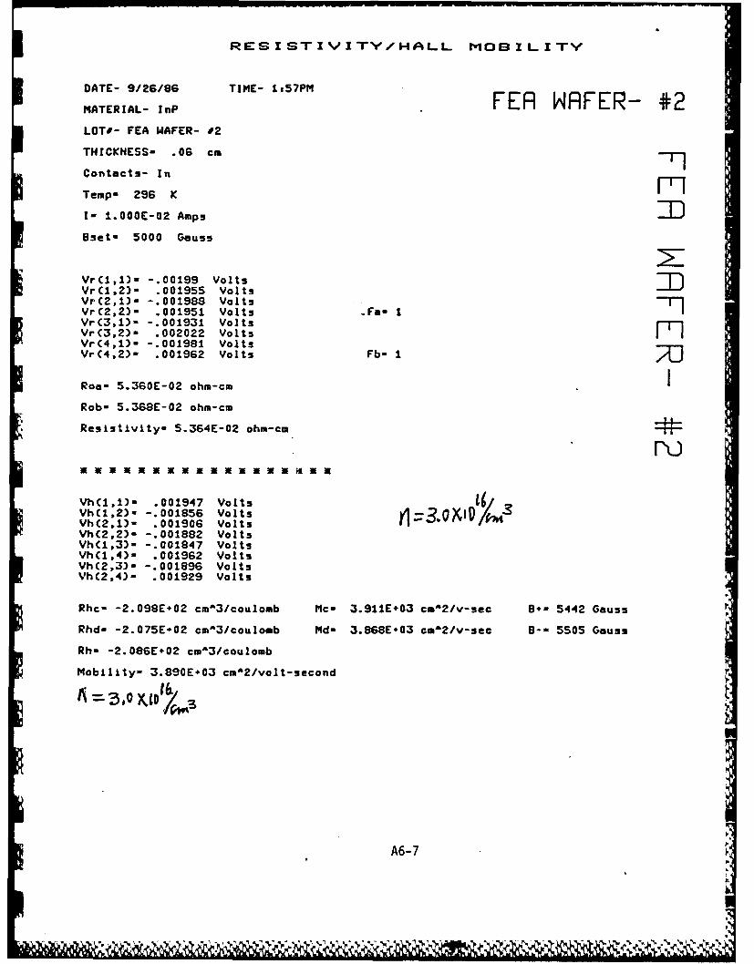
A6-9 Electrical Data for InP-4
A6-10 Electrical Data for InP-5
A6-11 Photocopy of GaAs Hall Sample Sites
A6-12 Electrical Data for GaAs-Al
A6-13 Electrical Data for GaAs-A2
A6-14 Electrical Data for GaAs-A3A6-15 Electrical Data for GaAs-BlA6-16 Electrical Data for GaAs-B2
A6-17 Electrical Data for GaAs-B3
ILIINM~I

CK
CD-a
A6- 1
MWILAW 11

RESISTI VITY/HALL MOB I LI TY
DATE- 10/22/86 TIME- 12s32PM
..MATERIAL- CdS-j DE86016-03-20LOT*- DE86016-03-20
THICKNESS .055 cm
Contacts- In
Temp- 296 K
I I.O000E-03 Amps cDBset- 3000 Gauss
VrC1,1)- -.004047 VoltsVr(l,2)- .003964 VoltsVrC2,1)- -.001858 Volts --VrC2,2)- .001749 Volts Va- .95Vr(3,1)- -. 003934 VoltsVrC3,2)- .004072 VoltsVrC4,1)- -.001809 VoltsVrC4,2)- .001795 Volts Fb- .95
Roa- 6.878E-01 ohm-cm CRob- 6.874E-01 ohm-cm
Resistivity- 6.S76E-01 ohm-cm I
Vh(1,1)- .002398 VoltsVhCI,2)- -.002245 VoltsVhC2,1)- -.002035 VoltsVhC2,2)- .002107 VoltsVhCl,3)- .002156 Volts ,/VhCl,4)- -.001991 VoltsVhC2,3)- -.002288 VoltsVhC2,4)- .00235 Volts
Rhc- -2.264E.02 cmA3/coulomb Mc- 3.293E*02 cma2/v-sec B.- 3017 Gauss
Rhd- -2.285E*02 cmA3/coulomb Md- 3.324E+02 cm^2/v-sec B-- 2982 Gauss
Rh- -2.275E*02 cm^3/coulomb
Mobility- 3.308E.02 cm*2/volt-second
A6-2
~ ~ ~ ~ ~ ~ ~ ~ ~ ~ 4 , .. i %"" -' " "'' **;"4 %"' ; '""

AD-R174 "65 DEVELOPMENT OF A FREE CARRIER ABSORPT ION MEASUREMENT 2/2INSTRUMENT FOR ItdDlU (U) EAGLE-PICHER RESEARCH LASMIAMI OK SPECIALTY MATERIALS DIV 27 OCT 86
UNCLASSIFIED N8884-85-C-2438 F/G 26112 U
EEsoEmoEEEmiE
mh EmEh

1.0 .
11111!. 5111 .
I' 1.6
j44
RMPI-7
% %5.

RESISTIVITY/HALL MOBILITY
DATE- 10/22/86 TIME- 12s41PM
i .. MATERIAL- CdS-D
Us.- LOT#- DM86197-23-09
.: THICKNESS- .055 cm
Contacts- In
Temp- 296 K iiI- 1.OOOE-04 Amps
Bset- 3000 Gauss
-oVrC2,1)- -.003649 Volts -\jVrC2,2)- .003553 Volts Fe- .99VrC3,1,- -.002539 VoltsVrC3,2)- .002693 VoltsVr(4,1)- -.003625 VoltsVrC4,2)- .003569 Volts Fb- .99 RURoa- 7.671E#00 ohm-cm
Rob- 7.666E+00 ohm-c.
Resistivity- 7.669E*00 ohm-cm CD
SVhC1,1)* -.0007559 VoltsVhC1.2)- .000898 VoltsVhC2.1)- .01165 VoltsVhC2,2). -.001108 Volts n= I, IOA3VhCl,3)- -.001057 VoltsVhCl,4)- .001209 VoltsVhC2,3)- .0008527 VoltsVhC2,4)- -.0007995 Volts
Rhc- -2.79Z3E03 cm^3/coulomb Mc- 3.642E*02 cm^2/v-sec B- 3013 Gauss
Rhd- -2.868E+03 cm^3/coulomb Md- 3.740E+02 cm^2/v-sec B-- 2980 Gauss
S. Rh- -2.831E.03 cm3/coulomb
Mobility- 3.691E*02 cm^Z/volt-second
{ A6-3.I ,.

RES IST '' V I'YHALL_ MOB IL I TV
. DATE- 10/22/86 TIME- 12,49PM
MATERIAL- CdS-3 DP86213-02-04LOT#- DP86213-02-04
THICKNESS- .055 cm
Contacts- In
Temp- 296 K UI- 1.000E-04 Amps coBset- 3000 Gauss
VrCII,)- -.007008 VoltsVrC1,2)- .006932 VoltsVrC2,1)- -. 009042 Volts (VrC2,2)- .008933 Volts Fa- .99Vr(3,1)- -. 006884 VoltsVrC3,2)- .007047 VoltsVr(4,i)- -.009007 VoltsVrC4,2)- .008952 Volts Fb- .99 (
Roa- 1.969E+01 ohm-cm
Robs 1.968E+01 ohm-cm
Resistivity- 1.9"8E+0i ohm-cm
.4S.
VhC1,1)- -.001526 VoltsVhC1,2)- .001656 VoltsVhCZ,1) .002477 Volts
* Vh(2,21m -,00241 Volts rVhCt,3)- -.002364 VoltsVhC1,4)- .002505 VoltsVhC2,3)- .001627 Volts
VhC2,4)- -.001563 Volts
Rhc- -7.691E-03 cm13/coulomb Mc- 3.308E+02 cm*2/v-sec B- 3015 Gauss
Rhd% -7.829E*03 cma3/coulomb Md- 3.978E402 oma2/v-sec B-- 2981 Gauss
Rh- -7.760E+03 cm'3/coulomb
Mobility- 3.943E+02 cm^2/volt-second
A6-4
I.-o.. V

h £
A6- 5I'
~ ~A' -
"~ '\''
KA~~

j RES1IS-rIVITV,/HAL1L Moe I IY
flDATE- 9/26/86 TIME- 2s57PM
MATERIAL- lnP FEFI WAFER #1LOTl TEA WAFER 01
THICKNESS- .06 cm ---IContacts- In
Temp- 296 K r-I- 1.OOOE-02 Amps liiiBset- 5000 Gauss
VrC1,1)- -.002156 VoltsZIVr(1b2)s .002009 Volts 1VrC2,1)- -.002171 Volts
_VrC2,2)- .002054 Volts 4&VrC3,13- -.001982 Volts1VrC3,2)- .002182 Volts M-VrC4,1)- -.002152 VoltsVrC4,2)- .002076 Volts Tb- 1 ~Z
Roa- 5.704E-02 ohsc
Rob- 5.70GE-02 ohm-cm*
Resistivity- 5.705E-02 ohm-cm
Vh(l,i)0 .001889 VoltsVh(1,2)- -.001723 VoltsVh(2,1)- .001923 VoltsVh(2,2)o -. 001834 Volts lr1/DVhC1,3)- -.001787 VoltsVh(i,4)- .001967 VoltsVhC2,3)- -. 001763 VoltsVh(2,4)- .001849 Volts
Rhc- -2.208E'02 cm^3/coulomb Mc- 3.870EJ0 cm^2/v-sec B.- 5004 Gauss
Rhd- -2.197E*02 cm*3/coulomb Mdo 3.952E#03 cm^2/v-sec 9-o 5031 Gauss
Rho -2.203E*02 cm^3/coulomb
Mobility- 3.861E#03 cm^2/volt-second
A6-6
111 Jill~iY
RESISTIVTY/HALL MOBILITv
DATE- 9/26/86 TIME- 1s57PM
MATERIAL- ,nP FER NRFER- #2LOT#- FEA WAFER- 02
THICKNESS- .06 cm
Contacts- In
Temp- 296 K i-I- i.OOOE-02 Amps lBset- 5000 Gauss
VrC1,1)- -. 00199 VoltslIVrC1,2)" .001955 VoltsVrC2,1) -.001988 Volts -T]VrC2,2)- .001951 Volts .Fa- IVr(3,i)- -.001931 VoltsVrC3,2)m .002022 VoltsVrC4,1)- -.001981 VoltsVr(4,2)- .001962 Volts Fb- 1
Roa- 5.360E-02 ohm-cm IRob- 5.368E-02 ohm-cm
Resistivity- 5.364E-02 ohm-cm #
VhC11)- .001947 VoltsVhC1,2)- -. 001856 VoltsVh(2,1)- .001906 VoltsVhC2,2)- -.001882 VoltsVhC1,3)- -.001847 VoltsVh(1,4)- .001962 VoltsVhC2,3)- -.001896 VoltsVhC2,4)- .001929 Volts
Rhc- -2.098E*02 cm^3/coulomb Mc- 3.911E+03 cmA2/v-sec B- 5442 Gauss
Rhd- -2.075E#02 cmA3/coulomb Md- 3.868E#03 cma2/v-sec 8-- 5505 Gauss
Rh- -2.086E*02 cmA3/Coulomb
Mobility- 3.890E+03 cmA2/volt-second
3A6-7ID
A6-7
p x

RES1ISTrIITVZHALU MOBIL ITV
DATE- 9/26/"6 TIME- 2O6PM F A 1A E - #MATERIAL- I nl AF R- #LOT#- FEA WAFER- 03
THICKNESS- .06 cm T9Contacts- In
-Temp- 296 K
I- 1.000E-02 Amps 1Bset- 5000 Gauss
VrC1,1)- -. 002193 VoltsVrC1,2)- .002092 Volts:1Vrc2,1)- -. 002186 Volts FVrC2,2)- .002111 VoltsFa IVi-C3,1)- -.002061 VoltsVr(3,2)- .002229 Volts iVi-C4,1)= -.002177 VoltsVrC4,2)- .002113 Volts Fb- 1
Roe- 5.834E-02 ohm-cm
Rob- 5.833E-02 ohm-cm
Resistivity- 5.834E-02 ohm-cm
VhCI,1)- .00211 Volts* VhCI,2)- -.00197 Volts
VhC2,1)- .002089 VoltsVhC2,2)- -.002017 Volts YVhCI,3)- -. 001985 VoltsVhCl,4)- .002142 VoltsVh(2,3)- -. 002018 Volts
* VhC2,4)- .002087 Volts
Rhc- -2.258E+02 cm^3/coulomb Mc- 3.870E*03 cm^21v-sec B.- 5453 Gauss
Rhd- -2.237E-02 cm43/coulomb Md- 3.835E*03 cm^2/v-5ec 8-- 5506 Gauss
Rh- -2.247E402 cm^3/coulomb
Mobility- 3.852E+0;5 cm*2/volt-5econd
A6-8

K RES ISTIVITVY/HAL. MOBILITY
DATE- 9/26/86 TIME- 239PM FEFI WAAFER 44MATERIAL- JnP
LOT#- FEA WAFER 04
THICKNESS- .06 cm -T]IIIIContacts- In 1-Temp- 296 K
I- 1.OOOE-02 Amps
Bset- 5000 Gauss
Vr(1,1)- -.002099 VoltsiIZVrC1,2)- .001982 VoltsVrC2,1)- -.002074 VoltsVrC2,23- .002017 Volts ;.a- 1 -VrC3,1)- -. 001953 VoltsVrC3,2)- .002125 VoltsVrC4,1)- -.002082 VoltsVrC4,2)w .002005 Volts Fb- I
Roa- 5.556E-02 ohm-cm
Rob- 5.551E-02 ohm-cm4=
Resistivity- 5.554E-02 ohm-cm
A 9XX3 N 3N 3K 3KE 3K 3NE K N M NX
VhC1,1)- .001879 Volts4 SVhC1,2)- -. 001711 VoltsVh(2,1)- .001816 VoltsVhC2,2)- -.001794 VoltsVh(i,3)- -.0017 VoltsVh(1,4)- .001873 VoltsVhC2,3)- -.001762 VoltsVh(2,4)- .001792 Volts
Rhc- -2.150E+02 cm'3/coulomb Mc- 3.871E*03 cm^2/v-sec 8- 4999 Gauss
Rhd- -2.15SE*02 cm*3/couloob Md- 3.SSGE#03 cm^2/v-sec 8-- 4980 Gauss
Rh- -2.154E*02 cm^3/coulomb
Mobility- 3.878E#03 cm^2/volt-second
A6-9

RESISTIVTV/HALL MOBILITY
DATE- 9/26/88 TIME- 2a47PM.,, ., _ ,.,FER IFRFER- #5MATERIAL- InP E WA R-*
LOT#- FEA WAFER- 05
THICKNESS- .06 cm -1
Contacts- In
Tempo 296 K
I- 1.OOOE-02 Amps 11Bset- 5000 Gauss
Vr(l,1)- -.002158 VoltsVr(1,2)- .002042 VoltsVrC2,1)- -.002144 VoltsVrC2,2)- .002064 Volts Fa- 1Vr(3,1)- -.002003 VoltsVrC3,2)- .002193 VoltsVrC4,1)- -.002146 VoltsVr(4,2)- .002062 Volts Fb- 1Roa- 5.716E-02 ohm-o J
Rob- 5.714E-02 ohm-cm
Resistivity- 5.715E-02 ohm-cm
VhC1,1)- .001924 VoltsVhC1,2)- -.001767 VoltsVh(2,1)- .00188 VoltsVh(2,2)- -.001841 VoltsVh(1,3)- -.001753 VoltsVh(1,4)- .001925 VoltsVh(2,3)- -.001803 VoltsVh(2,4)- .00185 Volts
Rhc- -2.209E 02 cm^3/coulomb Mc- 3.865E*03 cm^2/v-sec B- 5004 Gauss
Rhd- -2.221E*02 cmA3/coulomb Md- 3.885E*03 cm^2/v-sec 8-- 4981 Gauss
Rh- -2.215E+02 cm*3/coulomb
Mobility- 3.875E*03 cm'2/volt-second
ivi
A6-10

/0 savij'
cltoo47( Ga V
,f/4 $Ff .4 j 3X~
A6-11
IL-

RESISTIVITY/HALL MOBILITY
DATE: 9/19/ e6 TIME: 9:36.13
LOT #- Zrzooloei-Al
MATERIAL TYPE- GeAs
THICKNESS= 0.060 cm
TEMPfK)= 2906
I= 1. ()OE-''6
Bset= 5000 GAUSS
Vr (1, 1)- 0'.501 62e voltsYr~l,:2)= 0.0671019 voltsVr (2, 1)=-O. 07E0441 voltsVr(2D2)= 0. 0492447 voltsVr,1 ) =-O. 070 7231; volitsVr(.-,2)= 0.0571--5Z voltsYr (--. 1 ) =-0. 0440273 voltsVr (-1,2)= 0.033Z9428 volts
Fa=0.9 9 Fb=0.98
Roa= 1.Z6E+04 Rob= 1.40E+04
Resistivity= 1.72E+04 ohm-cm
Vh (1, 1)= 0. 0-80- 77 voltsVh (1,2)=-O. 0642879 voltsYh (2, i)=-o.o01866Z volts lVh (2,)=-O.076617e volts ~Yh (I. Z)=-o.0 18'204 volts gj ~~I"Vh(1,4)= lo.o0155oo voltsVh (2, 3) =-O.08e1:092 voltsVh(24) =0. 047Z654 volts
Rhc=-4. 69-E+07 Muc= 3Z. 393E+03 +B5003
Rhd=-4. 759E+07 Mu~d= 3. 447E.03 -B=50'25
Rh=-4.72;''E+07 cm^./coulomb
Mobil ity= 3. 420E+03Z cmA%2/volt-sec
A6-12

IRESISTIVITY/HALL MOBILITY
DATE: 9/18/ 86 TIME: 8:58.79
LOT #- Z00081-A2
MATERIAL TYPE- GaAs
THICKNESS= 0.060 cm
TEMP(K)= 296
I = 1 . OE-07
Bset= 500) GAUSS
Vr(1,1)=-0.0022821 voltsVr(1,Z)= 0.001778. voltsVr(2 1)=-0.0172380 voltsVr(2,2)= 0.0198334 voltsVr (3 1) =-0. 000569 voltsVr(3.2)= 0.0010635 voltsVr(4, 1)=-0. 0SSc)91 voltsVr(4,2)= 0.0186515 volts
Fa=O.71 Fb=0.72
Roa= 1.99E004 Rob= 2.04E+04
Resistivity= 2.01E+04 ohm-cm
Yh(1.1)=-0.0124911 voltsVh(112)= 0.0132339 voltsVh(2.1)= 0.0212.T15 voltsVh (.2) =-0. 0234890 volts 1'Vh C1. " ) =-O. 02250'4E0~ voltsVh(1,4)= 0.02307E5 voltsVh(2,3)= 0.0117e16 voltsVh(2. 4)=-O.O19085 volts
Rhc=-5. 81 IE+07 Muc= 2. 890E+03 +B=5007
Rhd=-5.693E+07 Mud= 2.832E+03 -B=5015
Rh=-5. 752E+07 cm^3/coulomb
Mobility= 2.861E+03 cm'2/volt-sec
A6-1 3
! ,~*---.*~.

RESISTIVITY/HALL MOBILITY
DATE: 9/18/ 86 TIME: 9:31.5
LOT #- 7700081-A7
MATERIAL TYPE- GaAs
THICKNESS= C..060 cm
TEMP (K) = 206
, ~I= 1.'0 -6
Bset= 5000 GAUSS
Vr(1, 1)=-0.055GS'S vclts
Vr(l.2)= 0.0642874 voltsVr(2 0)=-0. 042702 voltsVr C.2)= 0.0571784 voltsVr(Z. )=-0.0677472 vcltsVr(, '.2) 0.€0584884 voltsVr(4, 1)=-0.05257 0 5 voltsVr(4,2)= 0.0=2;771 volts
Fa=-. 99 Fb=C;. 99
Roa= 1.52E+04 Rob= 1.56E+'04
Resistivity= 1 .54E-0 - ohm-c,
Vh(i; I)= ( 1.0"4 10. voltsVh(1,2)=-0. 0599107 voltsVh("1)= 0.0257715 voltsVh 0:. :)=-,:24-92 voltsVh(I :) =-0. 0764474 voltsVh(.4)= 0.0296412 voltsVh (=4 -) =-0. 0627377 voltsVh(2.4)= 0.0564579 volts
Rhc=-5.286E+07 Muc= 3. 437E+0Z +B=4589
Rhd=-5. 312E+07 Mud= 3. 450E+03 -B=5009
Rh=-5.299E+-07 cm"./coulomb
Mobility= 3. 442E+0 cm2/volt-sec
A6-14
% .*
~ - - J

RESISTIVITY/HALL MOBILITY
DATE: 9/19/ 96 TIME: 10:29.*67
LOT #- ZZ.rO06 1-B1
MATERIA"L TYPE- GaAs
THICKN~ESS= 0.060 cm
TEMP(K)= 296
I= 1. 0OE-!)7
Bset= SOO': GAUSS
Vr (1, 1) =-O. 005194"Z4 voltsVr (1, ) =0. 004o9 6 voltsVr (2. 1)=-0. 0039946 voltsYr(2,2")= 0.0110160 voltsYr(Z 1) =-.0O,4158 voltsVr(Z;.'_)= 0.001?011 voltsVr(4.!)=-0.O0f7167 voltsVr(4,) O.OZ119SZ volts
Fa=0.P6 Fb=0.89
Roa= 1.96-'-704 Rob= Z.04E+'4
Resistivity= 2.EE04 ohm-cm
Yh(1. 1)=-O.OO271OZ voltsYh(1,2)=-0.OOO6171 voltsYh (2, 1)= 0. 02281 6S voltsVh(. ) -. 0 "~SO volts
Yh (1,Z) =-O. 01"78-51 voltsVh(1,4)- 0.0116727 voltsYhC2,%;)= 0.0161949 voltsYh (-",4) = 0. 00076S0 volts
Rhc=-6. 996E+07 Muc= 2. 709E+OZ +B=5010
Rhd=-7.146E.07 Mud= 2.858E+OZ -B=50z1
Rh=-7. 071E+07 cm^Z/coulomb
Mobility= 2.e28E.03 cm,*2/valt-secI
A6-15

I l I I I III I IE m I l I I _ __,_ • .
I
RESISTIVITY/HALL MOBILITY
DATE: 9/18/ 86 TIME: 10:4233
LOT #- 3300081-B2
MATERIAL TYPE- GaAs
THICKNESS= 0.060 cm
TEMP(K)= 296
I= 1.OOE-08
Bset= 500O GAUSS
Vr(1, 1)=-0.0232332 voltsVr(1,2)= 0.0088491 voltsVr-(2. 1) =-0. 0018086 voltsVr(2:2)= 0.0067191 voltsVr( 1)=-O. 0123550 voltsVr-(3,2)= 0.02"9757 voltsVr(4. 1)=-0.0043160 voltsVr(4.:2)= 0.0044330 volts
Fa=O.S7 Fb=0.S6
Roa= 2.40E+05 Rcb= 2.58E+05
Resistivity= 2.49E+05 ohm-cm
Vh(1,1)= 0.0359 voltsVh C1.2) =-0.0169514 voltsVh(2:1)=-0.0022388 voltsVh(2.)= 0.0150121 voltsVh(1.Z)= 0.0134366 volts
VhC1,4)= 0.0007944 voltsVh (2Z)=-O.0200140 voltsVhC.4)= 0.0331684 volts
Rhc=-1 006E+09 Muc= 4. 038E+03 +B=4906
Rhd=- •01E+09 Mud= 4.338E+03 -B=4988
Rh=-1. 04.E+09 cm^%/coulomb
Mobility= 4.188E.03 cm^2/volt-sec
A6-16
" - . -

RESISTIVITY/HALL MOBILITY
DATE: 9/18/ 26 TIME: 9:43.65
LOT #- ZZ:oooel-B
MATERIAL TYPE- GaAs
THICKNESS= 0.060 am
TEMF(K)= 296
1= !.00:E-06
Bset= 5000 GAUtSS
Yr (1. 1) =-O. 0E02922- voltsVi-(1,2)= 0.0667188 voltsVr (2, 1) =-O. 020 1842 voltsVr(C7,2)= 0.0589700 voltsVr(Z, 1)=-0. 0652197 voltsVr('.:)= 0. 0926795 voltsYr(4, 1)=-t0.040S547 voltsVr(4.2)= 0.0471467? volts
Fa=091? Fb=0.97
Roe= 1.W""E*04 Rob= 1.60E+04
Res i stivitv= 1. 46E-1-04 ohm-cim
Yh(1.1)= 0.1274415 voltsVh (1r2)=-0.0749840 voltsYh (2.,1) =0. 0160625 voltsVh C2.2)=--0.05S77260 voltsYh (1 ,Z) =0. 023827SC voltsYh C1. 4) = 0. 02 16091 voltsVh (24 ") -0. 0600649 voltsVh(2,4)= 0.0259571 volts
Rhc=-5.21"/E+07 Muc= 3.989E+O03 +B=50zz3
Rhd=-5. 389E+07 Mud- 3.696E+03 -B=5006
Rh=-5. 60ZE+07 cm^Z/coulomb
Mob ili ty- 3. 843E+03 cm"2/vol t-sec
A6-17

ATTACHMENT #7
FEA Data and Free Electron Density Maps
Page # Content
A7-1 Results for Sample CdS-l
A6-2 Results for Sample CdS-2
A7-3 Results for Sample CdS-3
A7-4 Results for Sample InP-l
A7-5 Results for Sample InP-2
A7-6 Results for Sample InP-3
A7 -7 Results for Sample InP-4
A7-8 Results for Sample InP-5
A7- Resuls for ample nP-5

FILE: CUB!SAMPLE- DE96016-03-20IO= 20.5 Tast3aicron)z 73.0%ALPHAID(AVE)= .405 C(av)- 1.47E-17RI2 .1561 Tas(10.6aicron)z 49.0%n(ave)= 2.75E+16
DATA 13.4 14.2 13.5 14.2 14.3 BETA .916 .929 .919 .929 .93015.0 13.7 13.2 12.9 13.9 .941 .921 .913 .909 .92413.6 13.3 12.4 13.2 12.7 .919 .915 .901 .913 .90613.9 13.5 12.5 11.9 12.6 .924 .919 .903 .892 .90413.4 12.9 12.9 11.9 11.5 .916 .909 .907 .892 .98712.4 12.9 12.6 12.2 13.0 .901 .909 .904 .998 .91012.8 14.9 12.8 12.0 11.9 .907 .938 .907 .995 .99223.4 27.1 15.5 16.8 9.1 1.069 1.125 .953 .968 .8515.6 4.6 6.3 9.1 9.4 .797 .792 .909 .836 .940
13.2 20.0 27.5 26.0 24.5 .913 1.017 1.131 1.108 1.085
1 T 65.4% 69.3% 65.9% 69.3% 69.8%EXP .722 .756 .727 .756 .76173.21 66.8% 64.4% 62.9% 67.9% .790 .735 .714 .701 .74466.3% 64.91 60.5% 64.4% 62.0% .731 .718 .679 .714 .69267.9% 65.9% 61.0% 57.61 61.5% .744 .727 .683 .652 .6965.4% 62.9% 62.4% 57.6% 56.1% .722 .701 .696 .652 .63860.5% 62.9% 61.5% 59.5% 63.4% .679 .701 .689 .670 .70562.41 72.2% 62.4% 58.5% 57.6% .696 .781 .696 .661 .652114.1%132.2% 77.1% 82.0% 44.4% 1.100 1.219 .922 .862 .52527.3% 22.4% 30.7% 39.5% 41.0% .344 .297 .382 .475 .49164.4% 97.6Z134.1%126.82119.5% .714 .982 1.230 1.184 1.136
ALHPAID .325 .279 .319 .279 .274 n 2.20E+16 l1.89E16 2.16E16 1.99E+16 1.96E+16.236 .307 .337 .355 .296 1.60E+16 2.09E+16 2.29E+16 2.41E+16 2.01E+16.313 .331 .397 .337 .369 2.12E+16 2.25E.16 2.63E+16 2.29E+16 2.50E+16.296 .319 .391 .429 .374 2.01E+16 2.16E416 2.59E+16 2.90E+16 2.54E.16.325 .355 .362 .429 .449 2.20E+16 2.41E 16 2.45E+16 2.90E+16 3.04E 16.387 .355 .374 .401 .349 2.63E.16 2.41E+16 2.54E 16 2.72E+16 2.37E+16.362 .247 .362 .414 .429 2.45E+16 1.67E+16 2.45E+16 2.81E+16 2.90E+16-.095 -.197 .196 .149 .644 11111111111111U l .33E016 1.O1E 16 4.37E+161.068 1.247 .963 .743 .712 7.25E+16 9.46E+16 6.53E+16 5.04E+16 4.93E+16.337 .019 -.207 -.169 -.127 2.29F+16 1.23E+15 I:l:tl t sit SS
A7-1 l

FILE: COS2SAMPLE- DM86197-23-0910: 21.9 Tas(3micron): 73.OZALPHAID(AVE)z .405 C(ave): 1.47E-17RI2 .1561 Tas(10.6,icron)z 48.On(ave)x 2.75E+16
DATA 20.4 19.1 22.3 19.2 17.9 DETA 1.003 .994 1.030 .996 .96721.6 19.2 20.0 20.1 20.4 1.020 .986 .997 .999 1.00321.1 21.2 20.1 24.7 24.4 1.013 1.014 .999 1.064 1.06019.9 23.3 25.7 23.5 21.9 .996 1.044 1.079 1.047 1.02425.6 21.0 20.0 19.3 21.3 1.077 1.012 .997 .997 1.01621.4 20.8 19.6 20.3 20.5 1.017 1.009 .992 1.002 1.00422.2 23.5 21.7 19.9 21.4 1.029 1.047 1.022 .996 1.01721.9 21.0 20.6 19.9 20.4 1.024 1.012 1.006 .996 1.00319.9 19.9 20.9 19.7 19.7 .992 .996 1.010 .993 .97919.5 19.4 19.1 19.6 19.4 .990 .999 .984 .992 .974
1 T 93.2% 87.21101.8% 87.7% 91.71EXP .949 .904 1.013 .907 .96099.6% 87.7% 91.3Z 91.8 93.2% .990 .907 .935 .939 .94996.3% 96.81 91.92112.6%111.4% .973 .976 .939 1.090 1.08190.91106.4%117.41107.31100.0% .932 1.046 1.121 1.052 1.000
116.9% 95.9% 91.3% 88.1% 97.31 1.119 .970 .935 .911 .99097.7% 95.0% 99.5% 92.7Z 93.6% .983 .963 .921 .946 .953101.4%107.3% 99.1% 90.91 97.7% 1.010 1.052 .993 .932 .993100.0% 95.9% 94.1% 90.9% 93.2% 1.000 .970 .956 .932 .94986.3% 90.9% 95.4% 90.0% 95.4% .896 .92 .966 .925 .98989.0% 88.6% 97.2% 89.5% 84.0% .918 .914 .904 .921 .878
ALHPAID .052 .101 -.013 .099 .151 n 3.54E+15 6.08E+15 I$111$136.61E+15 1.02E+16.010 .098 .067 .063 .052 6.94E#14 6.61E415 4.54E+15 4.29E+15 3.54E+15.027 .024 .063 -.087 -.078 1.95E+15 1.61E.15 4.29E+15 1:ssssss::::ssiMs1.071 -.045 -.115 -.051 .000 4.79E+15 uI811*IIU4UII:18U 3.01-.112 .031 .067 .094 .020 $111181112.09E+15 4.54E¢15 6.35E+15 1.38E+15.017 .038 .082 .056 .049 1.1SE+15 2.57E+15 5.56E+15 3.79E+15 3.30E+15-.010 -.051 .007 .071 .017 111111118111181:4.55E+14 4.79E+15 1.15E+15.000 .031 .045 .071 .052 3.01E+01 2.09E+15 3.05E+15 4.79E+15 3.54E+15.109 .071 .034 .079 .117 7.42E+15 4.79E+15 2.33E+15 5.31E+15 7.96E+15.096 .090 .101 .082 .130 5.82E+15 6.09E+15 6.89E+15 5.56E 15 8.79E+15
A7-2

L
FILE: CDS3SAMPLE= DP96213-02-0410= 20.5 Tas(3&icron)z 73.OALPHAID(AVE): .405 C(ave)= 1.47E-17R12= .1561 TasilO.6micron)= 48.OZn(avels 2.75E+16
DATA 20.5 21.7 20.9 20.5 25.5 BETA 1.024 1.043 1.030 1.024 1.10020.2 20.3 21.2 21.2 21.7 1.020 1.021 1.035 1.035 1.04319.7 19.4 21.0 19.7 19.7 1.012 1.009 1.032 1.012 1.01219.0 19.2 20.5 18.9 21.7 1.002 1.005 1.024 1.000 1.04318.7 20.0 18.9 15.0 26.2 .997 1.017 1.000 .941 1.11118.4 19.2 20.3 18.9 22.7 .992 1.005 1.021 .998 1.05821.3 20.0 18.9 18.9 18.7 1.037 1.017 .998 1.000 .99719.8 20.2 20.2 18.7 19.8 1.014 1.020 1.020 .997 .99919.4 17.8 17.4 17.9 25.5 1.009 .993 .977 .963 1.10019.1 20.3 20.5 21.9 31.9 1.003 1.021 1.024 1.046 1.199
I T 100.01105.9%102.0%100.0%124.4%EXP 1.000 1.042 1.014 1.000 1.16098.5% 99.0%103.4%103.41105.9% .999 .993 1.025 1.025 1.04296.1% 94.6%102.4% 96.11 96.1% .971 .960 1.019 .971 .97192.7Z 93.7Z100.0Z 92.2Z105.9% .946 .953 1.000 .942 1.04291.2% 97.6% 92.2% 73.21127.8% .934 .982 .942 .790 1.19099.81 93.7% 99.0% 91.71110.71 .923 .953 .993 .939 1.076103.91 97.61 91.71 92.2% 91.2% 1.028 .982 .938 .942 .93496.6% 98.5% 99.51 91.2% 91.7% .975 .999 .999 .934 .93894.6% 96.9% 84.9% 86.8%124.4% .960 .901 .965 .901 1.16993.2% 99.0%100.0%106.9%155.4: .949 .993 1.000 1.049 1.357
ALHPAID .000 -.041 -.014 .000 -.155 n 3.0E+01 1$111S11U1111111153.01E+01 111t18811.011 .007 -.024 -.024 -.041 7.31E+14 4.96E+14 $ IIIIIII$Issa:UII.029 .041 -.019 .029 .029 1.99E 15 2.75E+15 1111111181.98E+15 1.98E15.056 .049 .000 .060 -.041 3.90E+15 3.27E.15 3.O1E+01 4.06E+15 1511111.069 .019 .060 .236 -.174 4.60E15 1.23E+15 4.06E+15 1.60E 16 $ll$$tsl.080 .048 .007 .064 -.074 5.42E#15 3.27E+15 4.86E+14 4.33E+15 18111110-.028 .018 .064 .060 .068 I551151151.23E+15 4.33E+15 4.06E+15 4.60E+15.025 .011 .011 .069 .064 1.73E+15 7.31E+14 7.31E+14 4.60E+15 4.33E+15.041 .105 .122 .105 -.155 2.75E+15 7.115+15 9.27E+15 7.11E+15 18U1118$.052 .007 .000 -.048 -.305 3.53E+15 4.96E+14 3.O1EoI *1s1s111111111111
A7- 3
.

IiUA
FILE: INPISAMPLE= Y:10 TO 15 : 1=32 TO 3710= 47.2 Tas(3micron): 58.0% ALPHA$D(AVE)z .096 C(ave)= 3.35E-18R12 .2650 Tas(lO.boicron): 52.0% n(ave)= 2.87E 16
DATA 33.7 30.7 31.5 32.3 32.3 32.1 BETA .919 .985 .994 .903 .90329.5 33.4 33.7 33.0 32.1 32.1 .971 .915 .919 .911 .90132.3 34.1 33.3 32.3 32.6 32.7 .903 .923 .914 .903 .90634.2 32.4 31.2 31.9 32.4 31.7 .924 .904 .890 .899 .90435.1 31.6 31.3 31.3 30.5 30.2 .934 .995 .892 .992 .98332.7 32.9 30.5 30.4 30.3 31.7 .907 .910 .993 .881 .80
% T 71.4% 65.0% 66.7% 68.41 68.4% 69.0EXP .914 .766 .779 .792 .79262.5% 70.9% 71.4% 69.9% 68.0% 69.0% .745 .809 .814 .BO3 .78868.4% 72.2% 70.6% 69.4% 69.1% 69.3% .792 .920 .807 .792 .79672.5% 68.6% 66.1% 67.6% 68.6% 67.21 .921 .793 .774 .795 .79374.4Z 66.9% 66.31 66.31 64.61 64.0% .035 .780 .775 .775 .76269.3% 69.7% 64.6% 64.4% 64.2% 67.2% .799 .901 .762 .761 .759
ALHPAID .206 .267 .250 .234 .234 .238 n 6.17E+16 7.99E+16 7.48E+16 6.99E+16 6.99E+16.294 .212 .206 .220 .238 .238 8.78E 16 6.34E+16 6.17E+16 6.57E*16 7.11E+16.234 .199 .214 .234 .228 .226 6.99E+16 5.94E+16 6.40E+16 6.99E+16 6.81E+16.197 .232 .257 .242 .232 .246 5.88E I6 6.93E+16 7.67E+I6 7.23E+16 6.93E+16.190 .248 .254 .254 .272 .279 5.39E+16 7.42E.16 7.61E+16 7.61E+16 8.12E 16.226 .222 .272 .274 .276 .246 6.75E+16 6.63E+16 8.12E+16 B.IBE+16 9.25E+16
kt
A7-4
P%

FILE: INP2SAMPLE: Y:17 TO 22 :X:24 TO 29I0= 20.8 Tas(3aicron)x 58.0! ALPHAIDIAVE)z .096 C(ave): 3.35E-18R12: .2658 Tas(IO.6micron): 52.0% n(ave): 2.87E+16
DATA 15.2 15.0 14.7 15.0 16.3 15.9 BETA .928 .922 .915 .922 .95615.3 15.3 15.0 15.0 14.3 15.2 .930 .930 .922 .922 .90513.9 14.5 15.0 14.1 15.0 15.8 .894 .910 .922 .899 .92215.7 15.3 15.3 15.7 16.1 15.2 .940 .930 .930 .940 .95114.9 14.8 15.7 15.2 15.0 15.6 .920 .917 .940 .928 .92215.0 15.2 15.7 14.3 15.1 15.1 .922 .929 .940 .905 .925
1 T 73.1% 72.1! 70.7% 72.11 78.4% 76.4%EXP .926 .619 .808 .819 .86373.6% 73.6% 72.1% 72.1% 68.8% 73.1% .929 .929 .919 .819 .79466.8% 69.71 72.11 67.8% 72.1% 76.0% .779 .801 .819 .787 .81975.5% 73.6% 73.6% 75.5% 77.4% 73.1% .043 .829 .829 .943 .85771.6% 71.2% 75.5% 73.1% 72.1% 75.0% .915 .812 .843 .826 .81972.1% 73.1% 75.5% 68.8% 72.6% 72.6% .919 .826 .943 .794 .822
ALHPAID .191 .200 .213 .200 .147 .163 n 5.72E+16 5.97E 16 6.36E+16 5.97E+16 4.40E 16.187 .187 .00 .200 .231 .191 5.60E+16 5.60E 16 5.97E+16 5.97E+16 6.90E+16.249 .222 .200 .240 .200 .167 7.45E+16 6.63E+16 5.97E 16 7.17E+16 5.97E+16.171 .187 .187 .171 .155 .191 5.I0E+16 5.hOE+lb 5.60E+J6 5.IOE+lb 4.63E+lb.204 .208 .171 .191 .200 .175 6.10E+16 6.23E+16 5.10E+16 5.72E+16 5.97E+16.200 .191 .171 .231 .196 .196 5.97E+16 5.72E 16 5.10E+16 6.90E+16 5.95E+16
A7-5
ft".

FILE: INP3SAMPLE= Y=25 TO 30 :=32 TO 3710= 21.5 Tas(3sicron): 59.0% ALPHAID(AVE)= .096 Clave)= 3.35E-18R12: .2658 Tas(10.6.icron)= 52.0% nlave)- 2.97E+16
DATA 15.0 13.2 14.9 15.1 15.0 15.4 BETA .910 .865 .907 .912 .91016.0 15.1 15.1 15.3 15.0 14.7 .935 .912 .912 .917 .91016.6 14.7 15.2 15.1 14.6 14.4 .949 .903 .915 .912 .90011.7 14.7 14.4 15.0 15.9 15.5 .828 .903 .895 .910 .93012.4 13.9 16.7 15.0 14.9 14.2 .946 .883 .952 .910 .90715.0 16.2 15.2 15.1 14.5 14.2 .910 .940 .915 .912 .899
1 T 69.8 61.41 69.31 70.2% 69.8% 71.61EIP .802 .737 .798 .805 .80274.4% 70.2% 70.21 71.2% 69.8 68.41 .835 .805 .805 .912 .80277.21 68.4% 70.7% 70.21 67.91 67.0% .855 .791 .808 .905 .79954.41 68.41 67.0% 69.8% 73.5% 72.1% .678 .791 .790 .902 .82957.71 64.7% 77.71 69.8% 69.31 66.0% .706 .762 .958 .802 .79869.9% 75.31 70.7% 70.2% 67.4% 66.0% .802 .942 .909 .805 .784
ALHPASD .221 .306 .226 .217 .221 .204 n 6.61E+16 9.14E+16 6.74E+16 6.48E.!6 6.61E+16.190 .217 .217 .208 .221 .234 5.37E+16 6.48E+16 6.48E.16 6.23E+16 6.61E+16.156 .234 .213 .217 .239 .248 4.68E+16 7.01E416 6.36E+16 6.48E+16 7.14E+16.388 .234 .248 .221 .198 .200 1.16E+17 7.01E+16 7.41E+16 6.61E+16 5.61E+16.348 .271 .153 .221 .226 .257 1.04E+17 8.11E+16 4.56E+16 6.61E+16 6.74E+16.221 .172 .213 .217 .243 .257 6.6IE+1 5.l4E.16 6.36E+16 6.48E+16 7.27E+16
A-
A7 -
0. !

FILE: INP4
SAMPLE= Y=25 TO 30 : 1=17 TO 2210= 21.5 Tas(3aicron)= 58.01 ALPHAIDIAVE)= .096 C(ave)= 3.35E-18
R12= .2658 TasllO.6@icron)= 52.0% nlave)= 2.87E*16
DATA 15.7 14.6 14.4 14.3 14.7 15.2 BETA .927 .900 .895 .893 .90314.6 14.8 14.6 15.2 15.9 11.0 .900 .905 .900 .915 .932
14.3 14.3 15.0 15.4 16.0 16.2 .893 .893 .910 .920 .935
15.1 14.9 15.6 16.2 16.1 16.4 .912 .907 .925 .940 .93715.3 15.0 14.7 15.1 15.9 16.2 .917 .910 .903 .912 .932
15.1 15.0 15.2 15.1 15.5 15.8 .912 .910 .915 .912 .922
I T 73.0% 67.9% 67.0% 66.5Z 68.4% 70.7%EXP .825 .788 .780 .777 .791
67.9% 68.8% 67.9% 70.7% 74.0% 51.2% .786 .795 .788 .808 .832
66.5% 66.5% 69.8% 71.6% 74.4% 75.31 .777 .777 .802 .815 .83570.2% 69.3% 72.6% 75.3% 74.9% 76.3% .805 .798 .822 .942 .83971.2% 69.9% 68.4% 70.2% 74.0% 75.3% .812 .802 .791 .905 .B3270.2% 69.8% 70.7% 70.2% 72.1% 73.5% .805 .802 .808 .805 .819
ALKPAtD .192 .239 .248 .252 .234 .213 n 5.73E+16 7.14E16 7.41E+16 7.55E+16 7.01E+16.239 .230 .2439 .213 .184 .431 7.14E+16 6.87E+16 7.14E+16 6.36E+16 5.49E+16.252 .252 .221 .204 .180 .172 7.55E+16 7.55E+16 6.61E+16 6.10E+16 5.37E 16
.217 .226 .196 .172 .176 .164 6.46E+lb 6.74E+lb 5,96E+16 5.14E+16 5.25E l6
.208 .221 .234 .217 .184 .172 6.23E+16 6.61E16 7.01E+16 6.48E+16 5.49E 16
.217 .221 .213 .217 .200 .189 6.48E 16 6.61E 16 6.36E+16 6.48E+16 5.98E+16
A7-7
: ~ ~ ~ 1 % ~lvI

FILE: INP5SAMPLE= Y:10 TO 15 : X:17 TO 221O 21.5 Tas(3sicron): 5.0! ALPHAID(AVE)m .096 C(ave)z 3.35E-18R12z .2656 Tas(IO.6micron): 52.0% n(ave)= 2.87E#16
DATA 15.6 15.4 14.4 15.0 15.1 15.4 BETA .925 .920 .895 .910 .91214.7 14.7 15.T 15.6 15.4 15.3 .903 .903 .917 .925 .92015.3 15.6 15.7 15.0 15.0 14.9 .917 .925 .927 .910 .91015.0 14.8 15.0 15.1 14.8 15.1 .910 .905 .910 .912 .90515.6 15.0 15.1 15.0 15.5 15.2 .925 .910 .912 .910 .92216.0 16.0 15.7 16.0 15.9 15.9 .935 .935 .927 .935 .932
I T 72.61 71.61 67.0! 69.8% 70.2% 71.61EXP .622 .815 .780 .802 .60568.41 68.4% 71.2! 72.61 71.6% 71.2% .791 .791 .812 .822 .91571.2! 72.61 73.01 69.8! 69.6! 69.3! .812 .2 2 .825 .802 .80269.6! 68.8% 69.81 70.2% 68.8% 70.2% .802 .795 .802 .805 .79572.6% 69.81 70.2% 69.6% 72.11 70.71 .822 .802 .805 .802 .81974.4% 74.4% 73.0% 74.4% 74.0! 73.51 .635 .e35 .625 .635 .832 .4-
ALHPAID .196 .204 .246 .221 .217 .204 n 5.86E+16 6.10E+16 7.41E+16 6.61E+16 6.48E+16.234 .234 .208 .196 .204 .209 7.01E+16 7.01E+16 6.23E 16 5.86E+16 6.IOE+16.208 .196 .192 .221 .221 .226 6.23E+16 5.86E+16 5.73E+16 6.61E+16 6.61E+16.221 .2130 .221 .217 .230 .217 6.6JE.16 6.87E+lb 6.b6E+l6 6,4BE+16 6.B7E 16.196 .221 .217 .221 .200 .213 5.86E+16 6.61E+16 6.48E+15 6.61E+16 5.96E+16.180 .180 .192 .180 .184 .189 5.37E l6 5.37E.16 5.73E+16 5.37E 16 5.49E16,
, !.
.
A7-8
%.

Ruill, P