chapter 5 free carrier absorption in iii nitride...
TRANSCRIPT

99
Chapter 5
Free carrier absorption in III – nitride
semiconductors
5.1 Introduction
The absorption of electromagnetic radiation, due to its interaction with electrons in
semiconductors, is essentially determined by two distinct processes: interband and intraband
transitions. The electronic transitions may be direct or indirect according as the band extrema
occur at the same k or different k points in the Brillouin zone. The minimum photon energy
for interband absorption defines the fundamental absorption edge. In the second process,
namely, free-carrier absorption (FCA), electrons in the conduction band and holes in the
valence band are excited to higher energy states in the same band.
FCA, is essentially an intraband indirect transition phenomenon. It accounts for the
absorption of electromagnetic radiation of frequencies lower than those which give rise to
interband transitions and necessitates the mediation of phonons or imperfections to conserve
Part of the work presented in this chapter has appeared in
Journal of the Physical Society of Japan, 82, 043706 (2013)
AIP Conf. Proc., 1391, 72 (2011)
Proc. of 15th, International Workshop on Physics of Semiconductor Devices, XV, 579 (2009)

100
overall momentum. In the presence of phonons or imperfections a free carrier may absorb a
photon via a second order process in which the carrier changes its momentum by scattering.
FCA, intrinsically connected to scattering, is therefore a powerful means of determining the
possible scattering mechanisms operative and understanding transport properties in a system
[5.1].
In the last few years III–nitrides and their alloys have attracted attention as potential
material systems for use in high speed opto–electronic devices such as blue light-emitting
diodes (LEDs), blue lasers and solar blind ultraviolet photodetectors [5.2, 5.3]. The commonly
studied nitride–based compound semiconductors are GaN, InN and AlN whose room
temperature minimum band gaps range from 0.7 eV for InN through 3.4 eV for GaN to 6.2 eV
for AlN [5.3]. Among these, GaN, because of the large direct band gap and its chemical and
physical stabilities, has emerged as an attractive candidate for devices operating at high–
temperatures, high–voltages and high–power at microwave frequencies.
However, nitride semiconductor material systems, including GaN, InN and AlN are
known to be characterized by large built-in piezoelectric fields as well as the presence of
unintentional imperfections such as threading dislocations introduced during growth process,
due to lattice mismatch between substrate and active material. Threading dislocations can be
of the screw, edge and mixed types. Edge dislocations formed at the substrate-buffer interface
with mainly vertical orientation thread to the epilayer surface whereas the number of screw
and mixed dislocations are known to decrease with distance from the interface. The order of
edge dislocations is found to range from 107 cm
-2 to 10
10cm
-2 [5.2, 5.3]. However, in nitrides,
the dislocations parallel to the c – axis do not couple any piezoelectric potential [5.4]. These
edge dislocations are found to limit carrier transport properties considerably in nitride
101
quantum well systems [5.4] and are expected to influence performance of optical devices as
well.
The influence of dislocations on the optical absorption spectra of nitrides is found to
manifest in significant loss coefficients, and in enhancement of optical absorption near
fundamental absorption edge and a red shift of the absorption edge [5.5 – 5.10]. In GaN and
InGaN systems, Kioupakis and coworkers [5.11] employing the first principles approach, and
considering scattering by phonons, charged-defect and alloy scattering, have found FCA an
important loss mechanism. The peculiarities of FCA in InN epitaxial layers with wide range of
electron concentrations have been investigated by Nargelas et al [5.12] and Wu et al [5.13].
With a view to estimate the influence of dislocations on the FCA in nitride systems, we
have, in this chapter, made a study of FCA first in 2D QW systems and then in bulk nitride
systems. In section 5.3, we present our theory, developed for the first time, for FCA assisted
by dislocation scattering via Coulomb and strain fields in quantum wells. The absorption of
radiation by a free carrier is treated by a second-order perturbation in which the interaction of
the 2DEG with dislocations and with the radiation field is considered simultaneously.
Investigations of FCA in bulk nitrides are lacking. In section 5.4, we present a systematic
analysis of FCA coefficient in bulk GaN data considering electrons to be scattered by acoustic
phonons via deformation and piezoelectric interactions, impurities, optical phonons and
dislocations.
5.2 Theory
The FCA coefficient, K, is given by [5.1]
, (5.1)
102
where κ, is the dielectric constant of the medium, no the number of photons in the radiation
field and fi the carrier distribution function. The sum is over all initial states ‘i’ of the system.
Wi+ and Wi
- represent the transition probabilities for the absorption and emission of photons,
respectively and can be calculated using the standard second order Born golden rule
approximation. These are defined by
. (5.2)
In (5.2) the transition matrix elements are given by
, (5.3)
where Hrad is the electron-photon interaction Hamiltonian and VD the electron-dislocation
scattering potential. ħΩ is photon energy and Ei , Ej and Ef denote the initial, intermediate and
final state energies of electrons, respectively. The sum is over all the intermediate states j of
the system.
The expression for K can be evaluated using the wavefunction, eigenvalues and the
appropriate distribution function. The total FCA coefficient, K, due to various scattering
mechanism (s) is given by [5.1]: .
5.3 Free carrier absorption in nitride quantum wells
The edge dislocations are known to grow normal to the plane of the quantum well. The
electrons in quantum well are scattered by the dislocations via strain and coulomb interactions.
The scattering from the long range strain field surrounding the dislocations may be via
deformation and piezoelectric potentials.
In the case of 2D systems, FCA has been theoretically studied extensively in
GaAs/AlGaAs structures [5.14 - 5.16]. There are no systematic studies of FCA due to

103
dislocation scattering even in nitride quantum structures except for the investigation of Wu et
al in InN layers [5.13].
We consider a 2DEG in a square QW system with the electrons assumed to be
confined to move in the x-y plane. For simplicity, we consider the QW to be of infinite depth.
The electron wave functions and energy eigen values are given by [5.14]
, n = 1, 2… (5.4)
and
, (5.5)
where, is position vector, is electron wave vector, d is width of
the QW, n is the subband index and .
For a non-degenerate quasi 2D electron gas, the distribution function can be expressed
as [5.14]
, (5.6)
with,
, and ns is the sheet carrier concentration.
Assuming electromagnetic radiation to be polarized along the plane of the QW the
matrix elements of the electron–photon interaction Hamiltonian can be expressed as [5.14]
, (5.7)
where, e is unit vector in the direction of polarization of the radiation field.
5.3.1 Expression for dislocation-assisted FCA coefficient
FCA, which is intrinsically associated with carrier scattering through second order
process, requires a quantitative description of the dislocation scattering processes in a 2D

104
system. The scattering of the carriers by the edge dislocations in these systems is due to the
coulomb potential produced by the charges on the dislocation lines and the long-range strain
field surrounding the dislocation lines [5.4]. Dislocation scattering of 2DEG in QW systems
has been studied by many workers, considering the interaction of electrons with the strain
fields surrounding edge dislocations via deformation potential coupling [5.17, 5.18] and with
charged dislocations via coulomb potential [5.18]. Since the electric fields generated by
dislocations do not extend over large distances and are rather localized around the core of
dislocations, the screening of the interaction is weak. In the present work we consider the
interactions to be unscreened.
5.3.1.1 Dislocation scattering via strain field
The effect of strain field around dislocations is to shift the conduction and valence
band edges. The perturbing potential for electron scattering can be expressed as [5.17]
, (5.8)
where θ is the polar angle with respect to Burgers vector, b along QW plane, q is in-plane
wave vector, ac, the conduction band offset and γ the Poisson ratio.
Using eqns. (5.4) and (5.8) the expression for the matrix elements of electron-
dislocation scattering via strain interaction is expressed as
, (5.9)
where
, and is the angle between b and q. The
screening function with
. In the absence of screening
.

105
Using (5.1), (5.4), (5.6) and (5.9), we obtain the following expression for FCA
coefficient due to scattering by dislocations (of density Nd), via unscreened strain field
, (5.10)
where
,
,
and is exponential integral function and Nd is
dislocation density.
5.3.1.2 Dislocation scattering via Coulomb interaction
Modelling a threading dislocation, growing perpendicular to the QW plane, as a line of
charge with charge density ρL, we obtain the expression for interaction potential of electrons
with charged line dislocations as
,
(5.11)
where κw and κb are the dielectric constants of the material in well and barrier, respectively.
Assuming. κw= κb and using (5.11), we obtain the expression for the matrix element of
electron-dislocation scattering via coulomb field as
(5.12)
Here , , , and
.

106
Using (5.1), (5.4), (5.6) and (5.12), we obtain expression for FCA coefficient due to
scattering by dislocations (of density Nd) via unscreened coulomb interaction as
. (5.13)
Here
and
5.3.2 Results and Discussion
We have performed numerical calculations of FCA coefficient, K using equations
(5.10) and (5.13) considering scattering of electrons by edge dislocations. Here, we present the
results for three nitride quantum well systems of GaN/AlGaN, InN/AlN and AlN/AlGaN. The
material parameters, characteristic of GaN, AlN and InN, used in our calculations are given in
table 5.1.
Table 5.1:Material parameters of GaN, InN and AlN [5.3]
Parameter GaN InN AlN
Effective mass, m* (mo) 0.22 0.115 0.48
Conduction band offset, ac(eV) - 8.0 - 3.0 - 4.31
Burgers vector, b (Ǻ) 3.189 3.540 3.110
Poisson ratio, γ 0.3 0.42 0.287
Dielectric constant, ε 9.5 15.3 8.5
Lattice constant, c (Ǻ) 5.185 5.705 4.98

107
We choose to illustrate the behavior of FCA for quantum wells of width d = 100 Ǻ
and carrier concentration ns = 1 x 10¹¹
cm-2
. The dislocation line charge density, , is taken as
where f is the fraction of filled acceptor states and co , the lattice spacing in the (0001)
direction. We take Nd = 108 cm
-2, and assume f =1.
Figures 5.1, 5.2 and 5.3 depict respectively, the frequency dependence of the
dislocation–mediated FCA coefficient in GaN/AlGaN, InN/AlN and AlN/AlGaN quantum
well systems at T = 300K. In each of the figures 5.1, 5.2 and 5.3, curves a and b represent the
contributions to FCA from the strain field and the Coulomb field, respectively. Curves 1
denote the overall contributions. The following common features are noticed. For the
parameters and range of frequencies considered, the FCA coefficient decreases with increase
in photon frequency, . A kink is observed whenever the photon frequency equals
corresponding to transition to the second subband. It may be noted that, this kink occurring
along with the FCA process is peculiar to QW THz systems. This is incontrast to the bulk case
where, FCA and interband transitions occur as separate processes. The dominant contribution
to overall dislocation-mediated FCA is due to scattering via the strain field of the dislocations.
In the case of GaN QW, the large contribution to the total FCA (curve 1) from the strain field
(curve a) may be due to large conduction band deformation potential as compared to that of
InN and AlN. It is also noticed that, the position of the kink shifts towards higher (lower)
energy region for InN (AlN), as compared to that in GaN. This shift may be due to the varying
values of the effective masses of electron in the three systems (see table I). The value of the
FCA coefficient is found to be enhanced at the subband transition energy with the increase in

108
4 6 8 10 12 14 16 18 20
0.1
1
10
100GaN
b
1a
K (
10
3 c
m-1)
(1013
s-1)
Figure 5.1: Variation of dislocation mediated FCA coefficient, K, as function of photon frequency, ,
for the GaN quantum well of width d = 100 Ǻ, carrier concentration ns = 1 x 10¹¹
cm-2
and dislocation
density Nd = 1 x 108 cm
-2. Curves a and b depict K due to dislocation scattering via strain and coulomb
interactions, respectively. Curve 1 represents the total K.
4 6 8 10 12 14 16 18 20
2
4
6
8
10
12
1
InN
b
a
K (
10
3cm
-1)
( x 1013
s-1)
Figure 5.2: Variation of dislocation mediated FCA coefficient, K, as function of photon frequency, ,
for the InN quantum well of width d = 100 Ǻ, ns = 1 x 10¹¹
cm-2
and Nd = 1 x 108 cm
-2. Curves a and b
represent K due to dislocation scattering via strain and coulomb interactions, respectively. Curve 1
depicts the total K.

109
4 5 6 7 8 9 10
0.5
1.0
1.5
2.0
2.5
3.0
3.5
1
AlN
b
a
K (
10
3cm
-1)
( x 1013
s-1)
Figure 5. 3: Variation of dislocation mediated FCA coefficient, K, as function of photon frequency, ,
for the AlN quantum well of width d = 100 Ǻ , ns = 1 x 10¹¹
cm-2
and Nd = 1 x 108 cm
-2. Curves a
and b depict K due to dislocation scattering via strain and coulomb interactions, respectively. Curve 1
represents the total K.
absorption coefficient near the kink found to be larger for InN compared to that of AlN and
GaN. A comparison of the behavior of FCA in QWs due to scattering of 2DEG by dislocation
strain with that in bulk systems [5.13] shows the magnitudes of K to be larger in QW system.
This may be because the increased localization of charge within the 2DEG, could enhance
scattering of the 2DEG [5.17].
We have also investigated the influence of QW width and dislocation density on FCA.
In figure 5.4, curves 1, 2 and 3 show variation of FCA coefficient in GaN QWs with
Nd =108
cm-2
for well widths, d = 125 Ǻ, d = 100 Ǻ and
d = 75 Ǻ, respectively. It may be noted
that, the position of kink at redshifts with increase in well width. This is because the

110
Figure 5.4: Variation of dislocation mediated FCA coefficient, K as function of photon frequency, ,
for the GaN quantum well of ns = 1 x 10¹¹
cm-2
. Curves 1, 2 and 3 depict total K for Nd = 1 x 108 cm
-2
well widths, d = 125 Ǻ, d=100 Ǻ and d = 125 Ǻ, respectively. Curves 2, 4 and 5 depict the variation
of total K with dislocation density, Nd = 1 x 108 cm
-2, Nd = 1 x 10
9 cm
-2 and Nd = 1 x 10
10 cm
-2,
respectively for QW of width d = 100 Ǻ.
confined states of the well are closer in energy for larger well widths. Our results are
consistent with experimental studies of Bayram in AlGaN/GaN superlattices [5.19]. Curves 2,
4 and 5 depict the variation of FCA coefficient for the GaN QW of width d = 100 Ǻ for
dislocation densities, Nd = 1 x 108 cm
-2, Nd = 1 x 10
9 cm
-2 and Nd = 1 x 10
10 cm
-2,
respectively. An increase in number of dislocations results in an increase in FCA. This follows
from eqns. (5.10) and (5.13), indicating that larger loss coefficient can result from higher
dislocation densities [5.6]. It may be noted that a similar dependence is exhibited by 2DEG
scattering rate [5.4, 5.18], a first order scattering process.
In conclusion, we have developed a theory of edge dislocation assisted FCA in QWs
assuming the scattering via coulomb and strain fields. Calculations of frequency dependence

111
of FCA coefficients in QWs of three nitride systems – GaN ,InN and AlN – are presented.
The dominant contribution to the FCA is found to be due to the strain field of the dislocations.
The frequency dependence of FCA coefficients exhibits kinks whenever the frequency
corresponds to transition to the second subband. The position of kinks shows redshift with
increase in quantum well width. The theory shows larger loss (absorption) coefficients due to
increase in dislocation density [5.7]. It may be mentioned here that, the inclusion of the
screening of the interactions is expected to reduce the FCA coefficients. An estimate of the
effect of screening for large angle scattering (q = 2kF; , being Fermi
wavevector) in the QWs of GaN, InN and AlN indicates a reduction in the FCA coefficients
by approximately 20%, 13% and 42% respectively. It may be mentioned that, with proper
control of the parameters characterizing dislocations, one may obtain information about the
band structure of the QW system especially in those regions of the subbands might be
explored which cannot be reached by the electrons in an experiment on transport phenomena.
5.4 Free carrier absorption in bulk nitrides
Light absorption in nitrides arises because of scattering of free carriers from inevitable
acoustic phonons, via deformation potential and piezoelectric interaction, optical phonons and
unintentional impurities, and dislocations introduced during growth process. In particular,
FCA depends on the individual contributions due to various scattering mechanisms operative
in the system. Here, we are interested in investigating the influence of dislocation scattering on
FCA in bulk nitrides.
In literature, there exist, investigations of FCA in bulk semiconductors with regard to
dislocation scattering [5.6, 5.7]. However, the role and importance of the contribution from

112
dislocation scattering to FCA in GaN seems to be unclear. Cunninghaum et al [5.20] have
measured room temperature IR spectra for 3 GaN samples in the region of 1 < λ < 3.5μm.
Their measurements showed a characteristic FCA described by a wavelength dependence of
absorption coefficient s , with s ranging from 2.2 to 3.9, characteristic of optical mode(s
~ 2.5) and impurity (s ~ 3.5) scatterings. Vignaud and Farvacque [5.6] proposed that the low-
energy component of optical absorption in GaAs induced by strong electric fields resulting
from charged dislocations, may be observed only at low temperature. Ambacher et al [5.21]
used photothermal deflection spectroscopy to study the sub-band gap absorption of GaN thin
films in the range 0.6 – 3.6eV. They correlate the FCA below 1.5eV with electron
concentration and find s ~ 2. Hasegawa et al [5.22], who have recently measured optical
absorption spectra for plastically deformed n-GaN, have observed, in the long wavelength
region (λ > 1μm), a decrease in FCA by deformation.
The electron wavefunction and eigenvalues for a bulk semiconductor are (see (1.2) and
(1.3))
(5.14)
and
. (5.15)
The distribution function for a non-degenerate electron gas is
(5.16)
The FCA coefficient K, for bulk semiconductor can be obtained using expressions
(5.1), (5.2), (5.3) and (5.16) as [5.23]

113
(5.17)
where,
,
,
and being photon and phonon energies, respectively, and
.
In (5.17) the sum is over all scattering mechanisms, s, and , represents the matrix elements
for electron–phonon, electron–impurity, or electron–dislocation scattering interaction
Hamiltonian. The expressions for the electron-radiation and electron-imperfection scattering
interaction Hamiltonians are documented in literature [5.23, 5.24].
5.4.1 Analysis of FCA data in bulk GaN
We have performed numerical calculations of FCA coefficient, K using (5.17) for
parameters characteristic of bulk GaN (see table 5.1) [5.1] at T=300K in range of wavelength,
λ, 1 – 50μm. The other parameters used are typical of the GaN sample of Hasegawa [5.22]:
impurity concentration Ni = 5 x 1024
m-3
, dislocation density Nd = 1014
m-2
, and optical
phonon energy, ħωq = 91 meV.
114
100
101
102
103
104
105
106 d
1e
c
b
a
K (
m-1)
(m)
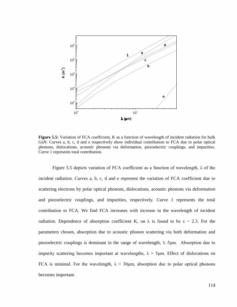
Figure 5.5: Variation of FCA coefficient, K as a function of wavelength of incident radiation for bulk
GaN. Curves a, b, c, d and e respectively show individual contribution to FCA due to polar optical
phonons, dislocations, acoustic phonons via deformation, piezoelectric couplings, and impurities.
Curve 1 represents total contribution.
Figure 5.5 depicts variation of FCA coefficient as a function of wavelength, λ of the
incident radiation. Curves a, b, c, d and e represent the variation of FCA coefficient due to
scattering electrons by polar optical phonons, dislocations, acoustic phonons via deformation
and piezoelectric couplings, and impurities, respectively. Curve 1 represents the total
contribution to FCA. We find FCA increases with increase in the wavelength of incident
radiation. Dependence of absorption coefficient K, on λ is found to be s ~ 2.3. For the
parameters chosen, absorption due to acoustic phonon scattering via both deformation and
piezoelectric couplings is dominant in the range of wavelength, 1–5μm. Absorption due to
impurity scattering becomes important at wavelengths, λ > 5μm. Effect of dislocations on
FCA is minimal. For the wavelength, λ > 30μm, absorption due to polar optical phonons
becomes important.

115
100
101
103
104
105
106
107
108
109
b
c
a
K (
m-1)
(m)
Figure 5.6: Variation of FCA coefficient in bulk GaN at 300K for three impurity concentration: 1019
m-3
(curve a), 1023
m-3
(curve b) and 1025
m-3
(curve c), m-3
.
In figure 5.6, curves a, b, and c show variation of FCA coefficient for impurity
concentration 1019
, 1023
and 1025
, m-3
at T = 300K respectively. For the parameters
considered, we find that, an increase of impurity concentration from 1023
to 1025
m-3
increases,
the absorption by one order of magnitude at λ = 1μm. The effect of impurity concentration is
large for higher wavelengths.
Figure 5.7 shows a comparison of our numerical results of FCA coefficient with the
measured data of Hasegawa [5.22] in GaN in the range of wavelengths 1 – 2 μm. For the
parameters considered a good fit is obtained. For the GaN sample considered we take impurity
concentration, Ni = 5 x 1024
m-3
and dislocation density Ndis = 1014
m-2
[5.2]. Curves a – e
denote individual contributions to FCA coefficient due to scattering of electrons from acoustic

116
1.0 1.2 1.4 1.6 1.8 2.0
0
1
2
3
4
5
c
b
a
d e
1
K (
mm
-1)
(m)
Figure 5.7: Variation of FCA coefficient in bulk GaN. Curves a, b, c, d and e represent the individual
contribution due to acoustic deformation, piezoelectric, impurity, dislocation and polar optical phonons
scatterings, respectively. Curve 1 denotes total contribution. Circles denote experimental data of [5.22].
phonons via deformation, and piezoelectric, impurities, dislocations and polar optical phonons,
respectively. Curve 1 represents total contribution. Circles denote measured data. K increases
with increase in wavelength of incident radiation. Dependence of K on wavelength is 2.3 and
it agrees with experiment. K, is found to be of the order of few mm-1
.
We find that, for the range of wavelengths the considered, contribution from acoustic
phonon scattering via deformation potential coupling is large compared to that from
piezoelectric phonon and impurity scatterings. The wavelength dependence for acoustic
phonons via deformation potential and piezoelectric couplings is same. FCA due to dislocation
and polar optical phonon scattering is small. It is also found that, the effect of impurity
scattering is more at higher wavelengths.

117
REFERENCES
5.1 H. J. Meyer, Phys. Rev. 112, 298 (1958).
5.2 O. Ambacher, J. Phys. D: Appl. Phys. 31, 2653 (1998).
5.3 H. Morcok: Nitride Semiconductors and Devices , (Springer-Verlag, Berlin 1999);
“Low Dimensional Nitride Semiconductors” ed. Bernad Gil, OUP (2002) p. 1.
5.4 M.D. Kamatagi, N. S. Sankeshwar, B. G. Mulimani: Phys. Rev. B 71, 124334 (2005),
references therein.
5.5 G. A. Slack, L J Schowalter, D Morelli and J A Freitas Jr, Journal of crystal growth 246,
287 (2002).
5.6 D Vignaud and J. L. Farvacque, phys. stat. sol. b, 156, 717 (1989).
5.7 D. Vignaud and J. L. Farvacque, J. Appl. Phys. 65, 1261(1989).
5.8 Z.L. Liau, R L Aggarwal, P A Maki, R J Molnar, J N Walpole, R. C Williamson and I
Meln Gailis: Appl. Phys. Lett 69, 1665 (1996); S. K. Milshtein and B. G. Yacobi, Phys.
Lett. 54, 465 (1975).
5.9 E. Peiner, A Guttzeit and H Wehmann: J. Phys: Condens. Matter 14, 13195 (2002).
5.10 Yonenaga Y Ohno, T Taishi, Y Tukumoto, H Makino, T Yao, Y Kamimura and K
Edagawa, Journal of Crystal Growth 318, 415 (2011).
5.11 E Kioupakis, P Rinke, A Schleife, F Bechsted, G. Chris and Van de Walle: Phys. Rev.
B, 81, 241201(R) (2010); E. Kioupakis, P. Rinke and Chris G. Van de Walle: Appl.
Phys. Express 3 082101(2010).
5.12 S Nargelas, R Aleksiejunas, M Vengris, T Malinauskas, K Jarasiunas and E Dimakis:
Appl. Phys. Lett. 95, 162103(2009).
5.13 J. Wu,W Walukiewicz, S . X. Li, R Armitage, J. C. Ho, E. R. Weber, E.E. Haller, H Lu,
W J Schaff, A Barcz and R Jakiela: Appl. Phys. Lett. 84, 2805(2004).
5.14 H. N. Spector: Phys. Rev. B, 28, 971(1983).
5.15 N. S. Sankeshwar, S.S.Kubakaddi and B. G. Mulimani: Pramana - J. Phys. 32,
149(1989).
5.16 G. B. Ibragimov: J. Phys: Condens. Matter, 14, 4977(2002), and references therein.
5.17 R. P Joshi,V Shridhara, B Jogai, P Shah and R. D. del Rosario: J. Appl. Phys. 93, 10046
(2003).

118
5.18 D. Jena, A. C. Gossard and U. K. Mishra: Appl. Phys. Lett. 76, 1707 (2000).
5.19 C Bayram: J. Appl. Phys, 111, 013514 (2012).
5.20 R. D. Cunningham, R. W. Brander, N. D. Knee and D. K. Wickenden J. Luminescence
5, 21 (1972).
5.21 O. Ambacher et al Solid. State Communications, 97 (5), 365 (1996).
5.22 H. Hasegawa, Y. Kamimura, K. Edagawa and I. Yonenaga, J. Appl. Phys. 102, 026103
(2007).
5.23 K. Seeger “Semiconductor Physics” Springer – Verlag Wein New York. 1973.
5.24 B. Podor, phys. stat. Sol. 16, K167 (1996).