characterization of the two-photon absorption carrier generation region in bulk-si diodes
TRANSCRIPT

CHARACTERIZATION OF THE TWO-PHOTON ABSORPTION CARRIER GENERATION
REGION IN BULK SILICON DIODES
By
Nicholas C. Hooten
Thesis
Submitted to the Faculty of the
Graduate School of Vanderbilt University
in partial fulfillment of the requirements
for the degree of
MASTER OF SCIENCE
in
ELECTRICAL ENGINEERING
August, 2011
Nashville, Tennessee
Approved:
Professor Robert A. Reed
Professor Ronald D. Schrimpf

ACKNOWLEDGMENTS
More often than not, the path to scientific understanding can seem like a lonely one. That
is ultimately not the case. Without the support of mentors, peers, friends, and family, scientific
progress would be impossible. With that in mind, it is with the deepest appreciation that I extend
my thanks to the fine people who helped make this work possible. Chief among them is my advisor,
Robert Reed, for his unfailing support and enthusiasm for the work. Credit is also due to other
members of Vanderbilt University’s RER group: Ron Schrimpf for technical guidance and editing
the manuscript; Marcus Mendenhall and Art Witulski for discussions that improved the overall
quality of the work; and Nelson Gaspard, Jon Ahlbin, and Nick Atkinson for their seemingly infinite
patience when it came to answering my questions about TCAD. Dale McMorrow and the staff of
the Naval Research Laboratory were instrumental in setting up and running the experiments. I
would also like to thank my sponsoring agencies, NASA and the Defense Threat Reduction Agency
through their basic research program for providing the funding that made this work possible.
A heartfelt thanks is also due to my friends and family for their continued support of my educa-
tional pursuits. It is good to know that despite all of the unreturned phone calls and emails during
many long nights spent in the lab or in front of a computer screen, there are still folks gracious and
understanding enough to continue to claim me as one of their own. For that, they will always have
my constant respect and appreciation.
ii
TABLE OF CONTENTS
Page
ACKNOWLEDGMENTS . . . . . . . . . . . . . . . . . . . . . . . . . . . . . . . . . . ii
LIST OF FIGURES . . . . . . . . . . . . . . . . . . . . . . . . . . . . . . . . . . . . . . iv
I Introduction . . . . . . . . . . . . . . . . . . . . . . . . . . . . . . . . . . . . . . . 1
II Background . . . . . . . . . . . . . . . . . . . . . . . . . . . . . . . . . . . . . . . 3
II.1 Physical Basis for Two-Photon Absorption and Gaussian Beam Parameters . . . 3II.2 The Simple TPA Model . . . . . . . . . . . . . . . . . . . . . . . . . . . . . . . 5II.3 Illustrative Calculations Using the Simple TPA Model . . . . . . . . . . . . . . . 9II.4 Pulse Height Analysis . . . . . . . . . . . . . . . . . . . . . . . . . . . . . . . . 12
III Experimental Test Methods and Design . . . . . . . . . . . . . . . . . . . . . . . . 15
III.1 Test Structures . . . . . . . . . . . . . . . . . . . . . . . . . . . . . . . . . . . . 15III.2 Experiment Setup and Laser Specifics . . . . . . . . . . . . . . . . . . . . . . . 16III.3 Measurement Procedure . . . . . . . . . . . . . . . . . . . . . . . . . . . . . . . 17
IV Impact of Beam Waist Diameter on Collected Charge . . . . . . . . . . . . . . . . 22
V Laser Pulse Energy Trends . . . . . . . . . . . . . . . . . . . . . . . . . . . . . . . 25
V.1 The Pulse Energy Dependence of the Charge Collection Profiles . . . . . . . . . . 25V.2 Comparison to Heavy Ion-induced Charge Collection . . . . . . . . . . . . . . . 28
VI Comparing the Simple TPA Model to Experimental Results . . . . . . . . . . . . . 31
VI.1 Simulation Specifics . . . . . . . . . . . . . . . . . . . . . . . . . . . . . . . . . 31VI.2 Simulated Charge Collection Profiles . . . . . . . . . . . . . . . . . . . . . . . . 34
VII Implications for TPA SEE Testing . . . . . . . . . . . . . . . . . . . . . . . . . . . 38
VIIIConclusions . . . . . . . . . . . . . . . . . . . . . . . . . . . . . . . . . . . . . . . . 41
REFERENCES . . . . . . . . . . . . . . . . . . . . . . . . . . . . . . . . . . . . . . . . 43
iii
LIST OF FIGURES
Figure Page
II.1 An illustration of the single-photon and two-photon absorption process in a semi-conductor. In (a), a photon having energy greater than the bandgap leads to thecreation of a single electron-hole pair. In (b), two photons of subbandgap ener-gies are absorbed simultaneously to create a single electron-hole pair. . . . . . . 3
II.2 Room temperature linear absorption spectrum of silicon for various light wave-lengths. . . . . . . . . . . . . . . . . . . . . . . . . . . . . . . . . . . . . . . . 4
II.3 The longitudinal profile of a Gaussian beam. Relevant beam parameters are labeled. 5
II.4 β2 as a function of laser wavelength for intrinsically doped silicon (black squares). 7
II.5 β2 as a function of photon wavelength for various doping concentrations in sili-con. A wavelength of 1.26 µm was used for the measurements reported in thiswork. . . . . . . . . . . . . . . . . . . . . . . . . . . . . . . . . . . . . . . . . 8
II.6 Electron-hole density plot for the two-photon excitation process in silicon as afunction of depth (z), plotted in electron-hole pairs per cm3. The dashed lines,labeled w(z), represent the longitudinal dependance of the beam waist. The beamradius at the waist used in the calculation was 0.7 µm. Other relevant laser andmaterial parameters are included in the figure legend. . . . . . . . . . . . . . . 10
II.7 Generated carrier density due to TPA processes in Si using the simple TPAmodel. Plotted are carrier densities along longitudinal cutlines through the centerof the plot shown in Fig. II.6. The x-axis in the figure corresponds to the y-axisin Fig. II.6. Carrier densities for two beam waist diameters and two energies areshown. . . . . . . . . . . . . . . . . . . . . . . . . . . . . . . . . . . . . . . . 11
II.8 A schematic of the PHA system used in this work. A pulse is generated in areverse-biased silicon diode (detector) by photon absorption. It then propagatesthrough the system, resulting in an output pulse whose amplitude correspondsto the total charge collected in the diode and whose shape is Gaussian. Thepulse heights are then binned according to their energy to produce a pulse heightspectrum, which can be calibrated in terms of energy or charge. . . . . . . . . . 11
II.9 A representative pulse height spectrum. The x-axis has been calibrated in termsof MeV by using the α emission of Am-241. The y-axis represents the numberof pulse amplitudes recorded for each energy on the x-axis. . . . . . . . . . . . 12
II.10 A calibration plot for a typical MCA. Knowing the value of the zero offset isnecessary to accurately calibrate the pulse height spectrum in terms of energy. . 13
iv
III.1 Cross sections of the two bulk silicon diodes used in this work. The device shownin (a) was fabricated by Sandia National Laboratories in a 0.25 µm process. Thedevice shown in (b) was fabricated in a 45 nm foundry process. . . . . . . . . . 15
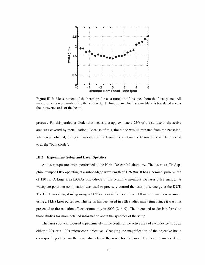
III.2 Measurement of the beam profile as a function of distance from the focal plane.All measurements were made using the knife-edge technique, in which a razorblade is translated across the transverse axis of the beam. . . . . . . . . . . . . 16
III.3 Diagram of the first step of the measurement procedure. The dashed line repre-sents the ”zero point” for the measurement. The plot on the right is a represen-tative data set used to show how the zero point in the cross section on the leftrelates to the data. . . . . . . . . . . . . . . . . . . . . . . . . . . . . . . . . . 18
III.4 The laser spot visually focused at the silicon dioxide/silicon interface for the epidiode, as imaged with a CCD camera in the beamline. . . . . . . . . . . . . . . 19
IV.1 Collected charge as a function of focal plane position and laser pulse energy fortwo different beam waist diameters. Values to the right of zero on the x-axesrepresent moving the focal plane deeper into the substrates of the devices. . . . 22
V.1 Collected charge as a function of laser pulse energy for the epi diode using a 1.4µm beam waist diameter. Values to the right of the zero point correspond to thefocal plane being inside the diode, while values to the left of zero correspond tothe focal plane being outside the diode. Similar data for the bulk device is shownin Fig.IV.1. . . . . . . . . . . . . . . . . . . . . . . . . . . . . . . . . . . . . . 25
V.2 The FWHM values of the charge collection profiles shown in Fig.V.1 for theepi diode as a function of increasing laser pulse energy. The increasing FWHMshows that, as the laser pulse energy increases, the carrier density in the wings ofthe TPA region is able to contribute to measurable charge collection, even whenthe focal plane of the beam is deep in the device substrate. . . . . . . . . . . . . 26
V.3 Peak collected charge as a function of laser pulse energy squared for the plotsshown in Fig.IV.1a and Fig.V.1. The pulse energy is squared to account for thedependence of the TPA-induced carrier density on laser pulse energy shown in(II.7). . . . . . . . . . . . . . . . . . . . . . . . . . . . . . . . . . . . . . . . . 28
V.4 Comparison between heavy ion and TPA-induced charge collection for the epidiode. The relationship between the square of the laser pulse energy and theheavy ion LET was determined empirically. . . . . . . . . . . . . . . . . . . . 29
v
VI.1 The two-dimensional epi diode as simulated in Sentaurus Device. Fig.VI.1ashows the entire simulated diode while Fig.VI.1b shows only a portion of thediode consisting of the n+ diffusion, p-epitaxial layer, and p+ substrate. The darkred region corresponds to silicon dioxide. Total doping concentration is plotted.The axes of each figure are in micrometers. The structure of the simulated bulkdiode was identical, only the substrate doping matched that of the epitaxial layer. 32
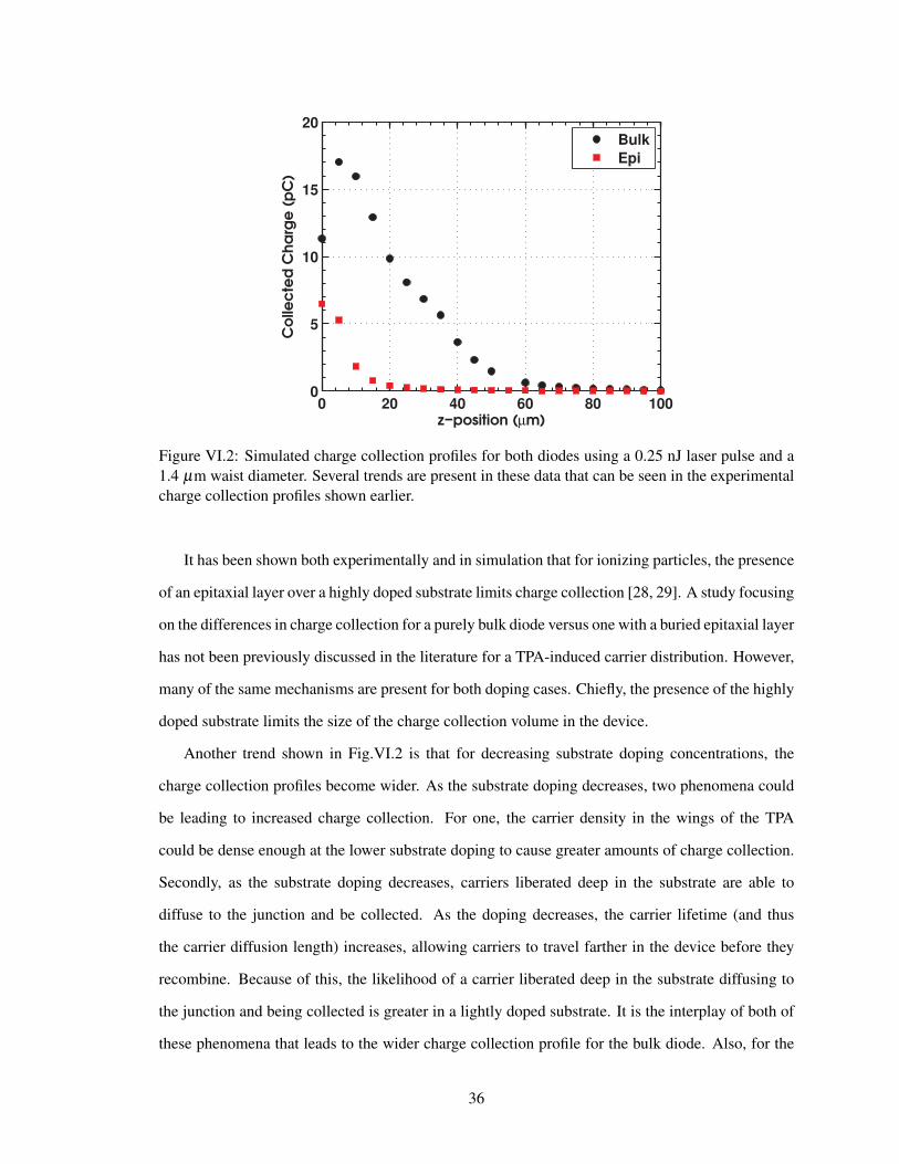
VI.2 Simulated charge collection profiles for both diodes using a 0.25 nJ laser pulseand a 1.4 µm waist diameter. Several trends are present in these data that can beseen in the experimental charge collection profiles shown earlier. . . . . . . . . 36
vi
CHAPTER I
Introduction
The pulsed laser has been a popular experimental method for interrogating single event effects
(SEEs) in microelectronic devices and circuits for many years [1]. While particle accelerator testing
is still considered to be the standard test method, the expense and availability of particle accelerator
facilities suitable for SEE testing can often be limiting factors in thoroughly characterizing devices
and circuits. Particle accelerator testing can also be destructive since devices can be exposed to a
very high fluence of radiation, potentially resulting in device degradation. In addition to being more
readily available and cost effective, laser testing offers deep insight into the spatial and temporal
characteristics of SEEs that can be difficult or impossible to determine with broadbeam particle
accelerator based test methods. Also, assuming the laser pulse energy is not excessively high,
device degradation can be completely avoided. Because of these factors, SEE laser testing is an
important resource for the the radiation effects community.
SEE laser testing is often performed using laser light wavelengths above the bandgap. In this
regime, Beer’s law absorption dominates, and it can be assumed that for every one energetic photon
incident on the semiconductor, one electron-hole pair will be created [1]. However, one limitation
of choosing this approach is that the total laser penetration will exponentially attenuate beginning
at the surface of the device under test (DUT). This requires that devices be tested from the topside,
through any device overlayer materials that may be present. As metallization densities increase
in device overlayers, topside laser testing can become difficult or impossible, due to shadowing
effects. This was one limitation of topside laser testing that lead to the development of two-photon
absorption (TPA) SEE laser testing [2].
TPA testing relies on the use of high peak-power femtosecond laser pulses at subbandgap optical
wavelengths. For wavelengths below the bandgap of the semiconducting material, few carriers are
generated at low light intensities [3, 4]. However, if the laser is highly focused, then in the region
near the focal plane where the intensity of the incident light is greatest, the material can absorb
two photons simultaneously to generate a single electron-hole pair. Because of this, carriers can
be deterministically injected at any location within the DUT. This avoids the limitations imposed
1
by dense overlayer metallization by allowing carriers to be injected from the backside, through
the substrate. This represented a significant step forward for SEE laser testing, and, since it was
first discussed as a test method in 2002 [2], it has been used many times to characterize the SEE
susceptibility of devices and circuits [2, 5–11].
Recently, there has been increased interest in trying to find a quantitative relationship between
TPA SEE testing and other well-established SEE test methods, such as heavy-ion irradiations, and
single-photon laser testing [12, 13]. However, very little experimental work has been reported that
describes the physical structure of the charge cloud centered on the focal plane where TPA carrier
generation occurs (the ”TPA region”). A detailed study of the carrier distribution produced in the
TPA region is important for any area of SEE testing where the spatial qualities of the injected carrier
density are significant. Specifically, TPA-induced latchup studies [14, 15] and studies that use TPA
as a method to investigate charge sharing between adjacent devices [8] could especially benefit from
a detailed knowledge of the charge distribution in the TPA region.
This work reports measurements of the spatial extent of the TPA region in the direction of beam
propagation in bulk-Si devices. This was accomplished through a combination of charge collection
measurements on large area diode structures and device-level technology computer aided design
(TCAD) simulations. The results indicate that the beam waist diameter of the laser can have a
significant impact on the peak carrier concentration and spatial distribution of carriers in the TPA
region. Experimental measurements also show that at sufficiently high laser pulse energies, the
location of where peak charge collection occurs in a device can shift away from the reverse-biased
junction. A simple analytical model describing the TPA-induced carrier density is discussed. This
model is then implemented in TCAD in an attempt to directly compare the results of the simple TPA
model to the experimental data. The simulation results show that while the simple TPA is sufficient
for analyzing qualitative trends in the data, a combination of factors relating to the experiment and
the simple TPA model itself prevent a meaningful quantitative comparison of the experimental data
to the simulation results.
2
CHAPTER II
Background
II.1 Physical Basis for Two-Photon Absorption and Gaussian Beam Parameters
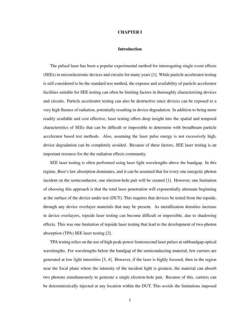
Conceptually, the TPA process is easy to understand. When the photon energy is greater than the
bandgap of the semiconducting material, one electron-hole pair is created for every absorbed photon.
However, if the energy of the incoming photons is less than the bandgap of the semiconductor,
two photons in close proximity can be absorbed simultaneously, leading to the creation of a single
electron-hole pair. Both of these processes are shown in Fig. II.1. By focusing the laser beam to
a small spot size, a high density of photons can be present in small area, which promotes the TPA
process. Fig. II.2 shows the room temperature absorption spectrum for silicon in the visible and
near-infrared regions of the electromagnetic spectrum. Common wavelengths used for laser SEE
testing are labeled. At wavelengths beyond 1200 nm, the linear absorption coefficient is negligible,
meaning that the vast majority of carriers created at wavelengths greater than 1200 nm is due to
multi-photon absorption processes. The laser wavelength used for this work was 1.26 µm, which
corresponds to a photon energy of approximately 1 eV.
The majority of laser beams used for SEE testing have Gaussian radial intensity distributions
[1]. The equations governing the propagation of Guassian beams in linear media can be derived
(a) (b)
Figure II.1: An illustration of the single-photon and two-photon absorption process in a semicon-ductor. In (a), a photon having energy greater than the bandgap leads to the creation of a singleelectron-hole pair. In (b), two photons of subbandgap energies are absorbed simultaneously to cre-ate a single electron-hole pair.
3

Figure II.2: Room temperature absorption spectrum of silicon for various light wavelengths. After[2].
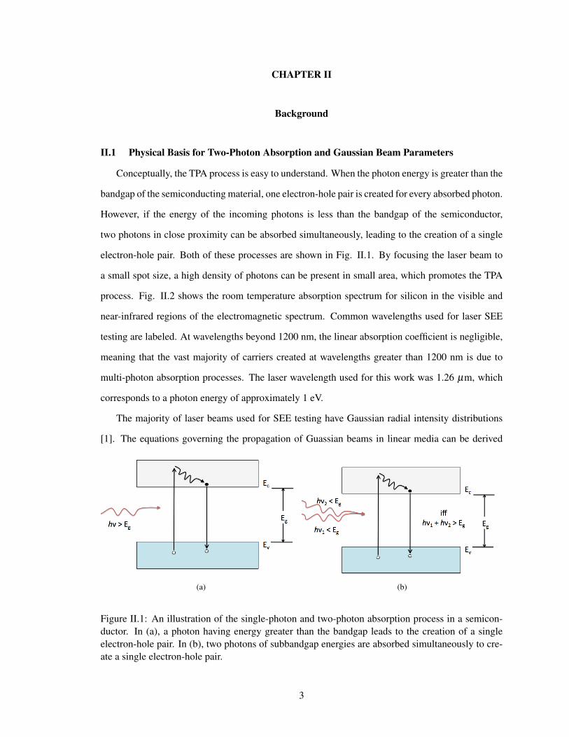
using the wave equation [4]. The longitudinal profile of a Gaussian beam can be seen in Fig. II.3.
The beam radius, w(z), is the point at which the laser intensity has decayed to 1/e of its peak value
and is given by:
w(z)2 = w2o[1+(
λ zπw2
on)2], (II.1)
where wo is the 1/e radius at the beam waist, λ is the wavelength, z is the direction of beam prop-
agation, and n is the index of refraction in the medium. The region of the beam within which wo
is less than or equal to√
2wo defines the confocal parameter of the beam. Mathematically, this is
expressed as
b =±πnw2o
λ. (II.2)
The parameter ZR is known as the Rayleigh range, and is equal to one half of the confocal
parameter. Two times the confocal parameter (2b) represents the range over which the beam is well
collimated within the vicinity of wo. Θ represents the total angular spread of the beam and is twice
the beam divergence. The radial dependence of the pulse irradiance is given by
I(r,z) =2P
πw2 exp(−2r2
w2 ) (II.3)
4
Figure II.3: The longitudinal profile of a Gaussian beam. Relevant beam parameters are labeled.
where P is the pulse power and r is the radial distance relative to the z axis (see Fig.II.3). The laser
pulse’s time dependence has been suppressed in this analysis.
A unique feature of a Gaussian beam is that the product of its width and divergence is the
smallest possible [16]. Because of this, once the beam is focused to a small spot, it spreads out
rapidly as it propagates away from that spot. While this is undesirable in laser applications that
require a well collimated beam over a long range, it is a benefit to TPA SEE testing as it helps to
confine carrier generation to the vicinity around the beam waist.
II.2 The Simple TPA Model
The equations governing pulse propagation and carrier generation in semiconductors are [2, 17,
18]
dI(r,z)dz
=−αI(r,z)−β2I2(r,z)−σexNI(r,z) (II.4)
dΦ(r,z)dz
= β1I(r,z)− γ1N(r,z) (II.5)
dN(r,z)dt
=αI(r,z)
h̄ω+
β2I2(r,z)2h̄ω
(II.6)
5
where I is the pulse irradiance, N is the density of free carriers, and Φ is the phase. Also, α is
the single-photon absorption coefficient, β2 is the two-photon absorption coefficient — which is
proportional to the imaginary part of the third-order nonlinear optical susceptibility (χ(3)) [19], β1
is proportional to the real part of χ(3), σex is the absorptivity of the laser-generated free carriers, and
γ1 represents the refraction due to free carriers. For (II.6), h̄ω is the photon energy, and the factor of
two in the denominator of the second term occurs as a result of two photons being absorbed simul-
taneously to generate one electron-hole pair. Said in words, (II.4) describes the optical absorption
experienced by a pulse propagating in the medium, (II.5) represents the phase change due to free
carriers and the laser pulse itself, and (II.6) is the time rate of change in the carrier concentration
due to single-photon and two-photon absorption. If a subbandgap laser wavelength is chosen, α in
these equations essentially goes to zero, meaning the contribution to the carrier generation due to
single-photon absorption is negligible, which reduces (II.6) to
dNT PA(z,r)dt
=β2I2(z,r, t)
2h̄ω. (II.7)
TPA is the result of a complex series of interactions between the nonlinear optical phenomena
that lead to the multi-photon absorption process and the semiconductor material itself. As such, a
full mathematical description in the most general case would involve solving (II.4)-(II.6) simulta-
neously using (II.1) and (II.3). Previous works have discussed the TPA process in qualitative terms
by solving (II.6) for N [2, 20]. While this does ignore optical effects that could have a significant
impact on the overall carrier generation (such as changes in the nonlinear index of refraction and
the effects of free carrier absorption with increasing carrier density), it does provide a qualitative
explanation of TPA in semiconductors.
If nonlinear absorption is the only loss mechanism in a material (as is the case when assuming
(II.7)), the irradiance as a function of depth in the material is
I(z) =Io
1+β2Ioz, (II.8)
6

Figure II.4: β2 as a function of laser wavelength for intrinsically doped silcon (black squares). After[21].
where Io is the beam irradiance at the waist. Finally, integrating (II.7) with respect to time yields
NT PA(z) =β2
2h̄ω
∫ +∞
−∞
I2(z, t)dt. (II.9)
The solution of (II.9) through the use of equations (II.1), (II.3), and (II.8) represents the simple
model for two-photon absorption, assuming that linear absorption is deemed to be negligible by the
selection of a proper wavelength of light. The ”simple” descriptor has been chosen to emphasize
that the model currently describes TPA only in the most simplistic of terms, without regard for any
higher order optical effects that could have an affect on the TPA-induced carrier density.
Obviously, several experimental parameters must be known to solve (II.9) for a specific case.
Some of these are governed by the individual experiment, such as the laser pulse power (P in (II.3)),
the beam waist size, and the wavelength of the laser. Other necessary parameters, while experimen-
tally derived, can be applied to a wider range of TPA experiments. These are the index of refraction
(n) and the two-photon absorption coefficient (β2). For the simple model, n is assumed to be con-
stant. The validity of this assumption is debatable, as some non-linear optical effects can change the
index of refraction. For this work, the index of refraction of silicon, n≈3.51, has been used.
The value of the two-photon absorption coefficient varies widely in the literature, however. Sev-
eral experimenters have measured β2 in silicon under a variety of circumstances, the most relevant
7
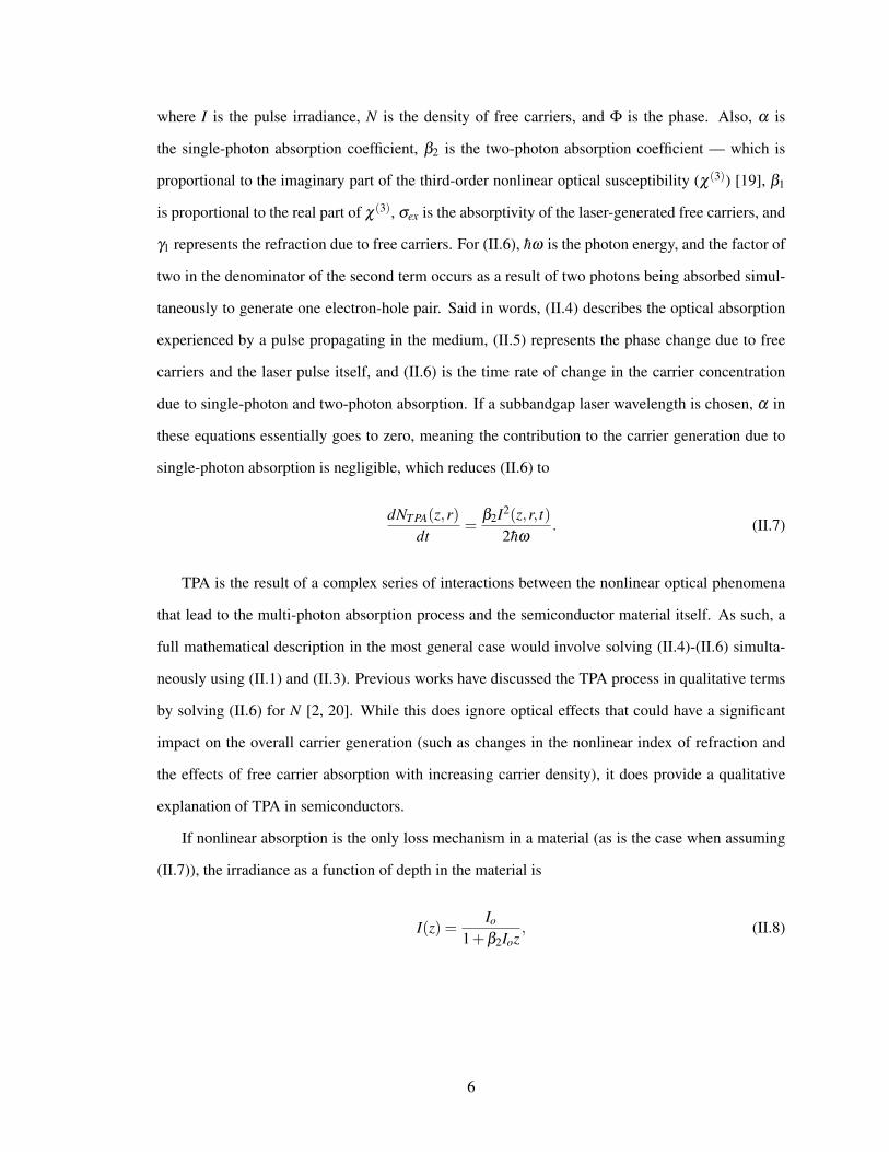
Figure II.5: β2 as a function of laser wavelength for various doping concentrations in silicon. Awavelength of 1.26 µm was used for the measurements reported in this work. After [22].
to this work being the measurement of β2 as a function of silicon doping and light wavelength.
The earliest reported measurements of β2 for bulk crystalline silicon were in [17], which reported
a value of 1.5 cm/GW. However, the wavelength used in that work was 1.05 µm, which is still
slightly in the region of linear absorption for silicon. The samples used to determine β2 in [17] were
also undoped (intrinsic). Lower silicon dopings tend to lead to higher values for β2 [22]. In [23],
a value for β2 of 0.74 cm/GW was reported for a laser wavelength of 1.27 µm at silicon dopings
(both p and n) of approximately 1015 cm−3. In [21], measurements of β2 in silicon at a variety of
wavelengths are reported. Their results can be seen in Fig. II.4. While this figure is illustrative of
how β2 changes as a function of wavelength in silicon, it should be noted that the black squares
represent β2 in intrinsically doped samples. The determination of β2 most relevant to this work is
that of [22], where β2 was determined as a function of both wavelength and doping. In [22], for
all tested doping concentrations (at a wavelength of 1.25 µm), the value of the TPA coefficient was
measured to be approximately 0.3 cm/GW. Because this value most accurately represents the de-
vices and experimental conditions used in this work, it was used in all calculations and simulations
involving β2.
8
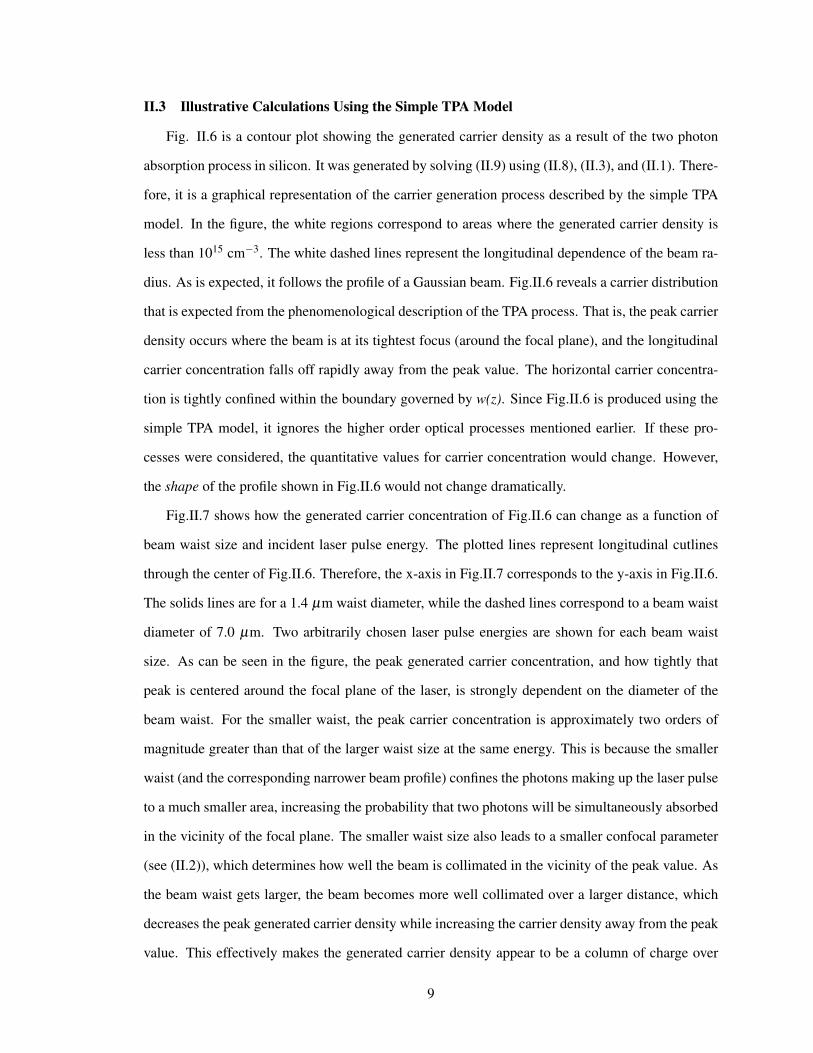
II.3 Illustrative Calculations Using the Simple TPA Model
Fig. II.6 is a contour plot showing the generated carrier density as a result of the two photon
absorption process in silicon. It was generated by solving (II.9) using (II.8), (II.3), and (II.1). There-
fore, it is a graphical representation of the carrier generation process described by the simple TPA
model. In the figure, the white regions correspond to areas where the generated carrier density is
less than 1015 cm−3. The white dashed lines represent the longitudinal dependence of the beam ra-
dius. As is expected, it follows the profile of a Gaussian beam. Fig.II.6 reveals a carrier distribution
that is expected from the phenomenological description of the TPA process. That is, the peak carrier
density occurs where the beam is at its tightest focus (around the focal plane), and the longitudinal
carrier concentration falls off rapidly away from the peak value. The horizontal carrier concentra-
tion is tightly confined within the boundary governed by w(z). Since Fig.II.6 is produced using the
simple TPA model, it ignores the higher order optical processes mentioned earlier. If these pro-
cesses were considered, the quantitative values for carrier concentration would change. However,
the shape of the profile shown in Fig.II.6 would not change dramatically.
Fig.II.7 shows how the generated carrier concentration of Fig.II.6 can change as a function of
beam waist size and incident laser pulse energy. The plotted lines represent longitudinal cutlines
through the center of Fig.II.6. Therefore, the x-axis in Fig.II.7 corresponds to the y-axis in Fig.II.6.
The solids lines are for a 1.4 µm waist diameter, while the dashed lines correspond to a beam waist
diameter of 7.0 µm. Two arbitrarily chosen laser pulse energies are shown for each beam waist
size. As can be seen in the figure, the peak generated carrier concentration, and how tightly that
peak is centered around the focal plane of the laser, is strongly dependent on the diameter of the
beam waist. For the smaller waist, the peak carrier concentration is approximately two orders of
magnitude greater than that of the larger waist size at the same energy. This is because the smaller
waist (and the corresponding narrower beam profile) confines the photons making up the laser pulse
to a much smaller area, increasing the probability that two photons will be simultaneously absorbed
in the vicinity of the focal plane. The smaller waist size also leads to a smaller confocal parameter
(see (II.2)), which determines how well the beam is collimated in the vicinity of the peak value. As
the beam waist gets larger, the beam becomes more well collimated over a larger distance, which
decreases the peak generated carrier density while increasing the carrier density away from the peak
value. This effectively makes the generated carrier density appear to be a column of charge over
9
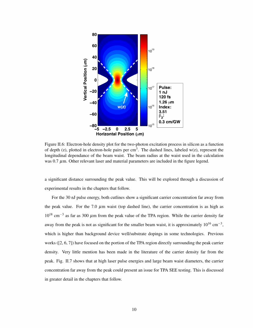
Figure II.6: Electron-hole density plot for the two-photon excitation process in silicon as a functionof depth (z), plotted in electron-hole pairs per cm3. The dashed lines, labeled w(z), represent thelongitudinal dependance of the beam waist. The beam radius at the waist used in the calculationwas 0.7 µm. Other relevant laser and material parameters are included in the figure legend.
a significant distance surrounding the peak value. This will be explored through a discussion of
experimental results in the chapters that follow.
For the 30 nJ pulse energy, both cutlines show a significant carrier concentration far away from
the peak value. For the 7.0 µm waist (top dashed line), the carrier concentration is as high as
1018 cm−3 as far as 300 µm from the peak value of the TPA region. While the carrier density far
away from the peak is not as significant for the smaller beam waist, it is approximately 1016 cm−3,
which is higher than background device well/substrate dopings in some technologies. Previous
works ([2, 6, 7]) have focused on the portion of the TPA region directly surrounding the peak carrier
density. Very little mention has been made in the literature of the carrier density far from the
peak. Fig. II.7 shows that at high laser pulse energies and large beam waist diameters, the carrier
concentration far away from the peak could present an issue for TPA SEE testing. This is discussed
in greater detail in the chapters that follow.
10
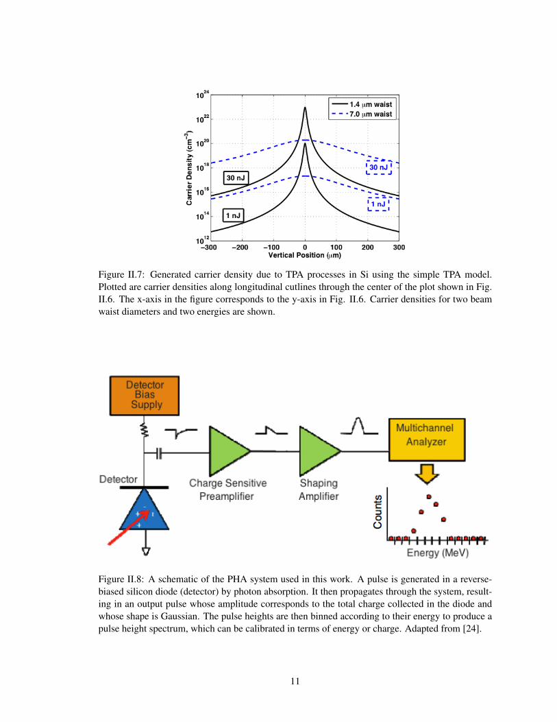
Figure II.7: Generated carrier density due to TPA processes in Si using the simple TPA model.Plotted are carrier densities along longitudinal cutlines through the center of the plot shown in Fig.II.6. The x-axis in the figure corresponds to the y-axis in Fig. II.6. Carrier densities for two beamwaist diameters and two energies are shown.
Figure II.8: A schematic of the PHA system used in this work. A pulse is generated in a reverse-biased silicon diode (detector) by photon absorption. It then propagates through the system, result-ing in an output pulse whose amplitude corresponds to the total charge collected in the diode andwhose shape is Gaussian. The pulse heights are then binned according to their energy to produce apulse height spectrum, which can be calibrated in terms of energy or charge. Adapted from [24].
11
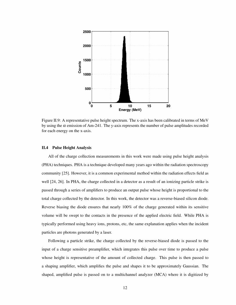
Figure II.9: A representative pulse height spectrum. The x-axis has been calibrated in terms of MeVby using the α emission of Am-241. The y-axis represents the number of pulse amplitudes recordedfor each energy on the x-axis.
II.4 Pulse Height Analysis
All of the charge collection measurements in this work were made using pulse height analysis
(PHA) techniques. PHA is a technique developed many years ago within the radiation spectroscopy
community [25]. However, it is a common experimental method within the radiation effects field as
well [24, 26]. In PHA, the charge collected in a detector as a result of an ionizing particle strike is
passed through a series of amplifiers to produce an output pulse whose height is proportional to the
total charge collected by the detector. In this work, the detector was a reverse-biased silicon diode.
Reverse biasing the diode ensures that nearly 100% of the charge generated within its sensitive
volume will be swept to the contacts in the presence of the applied electric field. While PHA is
typically performed using heavy ions, protons, etc, the same explanation applies when the incident
particles are photons generated by a laser.
Following a particle strike, the charge collected by the reverse-biased diode is passed to the
input of a charge sensitive preamplifier, which integrates this pulse over time to produce a pulse
whose height is representative of the amount of collected charge. This pulse is then passed to
a shaping amplifier, which amplifies the pulse and shapes it to be approximately Gaussian. The
shaped, amplified pulse is passed on to a multichannel analyzer (MCA) where it is digitized by
12
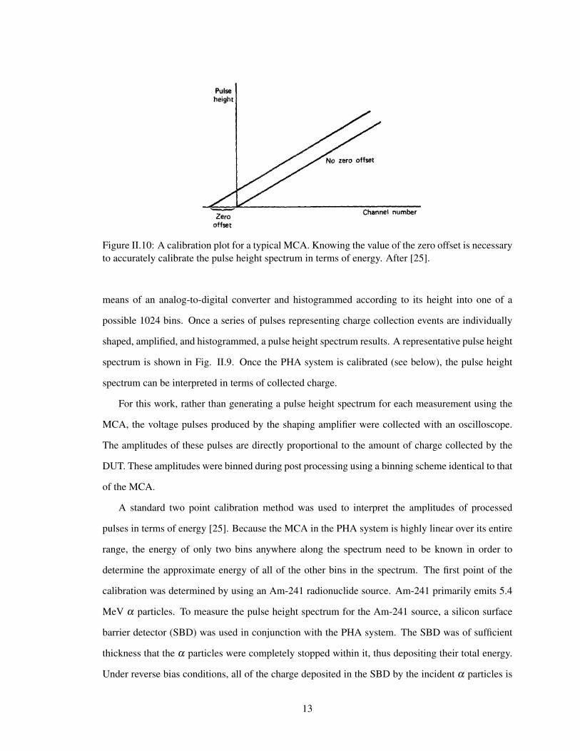
Figure II.10: A calibration plot for a typical MCA. Knowing the value of the zero offset is necessaryto accurately calibrate the pulse height spectrum in terms of energy. After [25].
means of an analog-to-digital converter and histogrammed according to its height into one of a
possible 1024 bins. Once a series of pulses representing charge collection events are individually
shaped, amplified, and histogrammed, a pulse height spectrum results. A representative pulse height
spectrum is shown in Fig. II.9. Once the PHA system is calibrated (see below), the pulse height
spectrum can be interpreted in terms of collected charge.
For this work, rather than generating a pulse height spectrum for each measurement using the
MCA, the voltage pulses produced by the shaping amplifier were collected with an oscilloscope.
The amplitudes of these pulses are directly proportional to the amount of charge collected by the
DUT. These amplitudes were binned during post processing using a binning scheme identical to that
of the MCA.
A standard two point calibration method was used to interpret the amplitudes of processed
pulses in terms of energy [25]. Because the MCA in the PHA system is highly linear over its entire
range, the energy of only two bins anywhere along the spectrum need to be known in order to
determine the approximate energy of all of the other bins in the spectrum. The first point of the
calibration was determined by using an Am-241 radionuclide source. Am-241 primarily emits 5.4
MeV α particles. To measure the pulse height spectrum for the Am-241 source, a silicon surface
barrier detector (SBD) was used in conjunction with the PHA system. The SBD was of sufficient
thickness that the α particles were completely stopped within it, thus depositing their total energy.
Under reverse bias conditions, all of the charge deposited in the SBD by the incident α particles is
13

collected. The collected charge is passes through the PHA system, ultimately resulting in a pulse
height spectrum once the system is allowed to process multiple pulses from the Am-241 source.
The centroid value of the resulting PHA spectrum is taken to be the mean energy of the incident α
particles (≈5.4 MeV for Am-241).
Due to the nature of the MCA in the PHA system, oftentimes the zero energy bin is not the
zeroth bin of the pulse height spectrum, but rather some bin close to it. This is known as the zero
offset of the MCA and is shown graphically in Fig.II.10. A pulser can be used to determine the
zero offset for a specific set of PHA system gain settings. By adjusting the magnitude of the pulses
injected into the PHA system by the pulser, a pulse height spectrum can be created that has multiple
peaks. By applying a linear fit to the centroid values of the peaks in the resulting pulse height
spectrum and extrapolating back to find the x-intercept of the linear fit, the actual zero energy bin
(or zero offset) can be found. This point can then be used as the second point of the two-point
calibration. By fitting a line between the two known energy bins (the bin corresponding to the
centroid of the Am-241 spectrum and the true zero energy bin), the energy of the other bins can
be calculated. This type of calibration might not be suitable for an application where the energy
must be known to a high degree of accuracy, but it is sufficient for this work. For silicon, energy
deposited generates charge with a known conversion factor of 22.5 keV/fC [27]. Therefore, once
the pulse height spectrum is calibrated in terms of MeV using the silicon SBD, it is a trivial matter
to calibrate it in terms of coulombs of charge as well.
14
CHAPTER III
Experimental Test Methods and Design
III.1 Test Structures
(a) Epi diode (b) Bulk diode
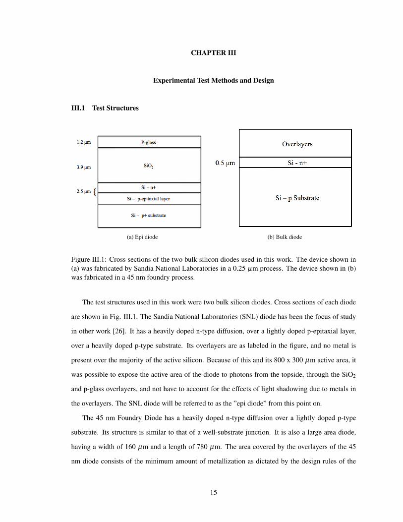
Figure III.1: Cross sections of the two bulk silicon diodes used in this work. The device shown in(a) was fabricated by Sandia National Laboratories in a 0.25 µm process. The device shown in (b)was fabricated in a 45 nm foundry process.
The test structures used in this work were two bulk silicon diodes. Cross sections of each diode
are shown in Fig. III.1. The Sandia National Laboratories (SNL) diode has been the focus of study
in other work [26]. It has a heavily doped n-type diffusion, over a lightly doped p-epitaxial layer,
over a heavily doped p-type substrate. Its overlayers are as labeled in the figure, and no metal is
present over the majority of the active silicon. Because of this and its 800 x 300 µm active area, it
was possible to expose the active area of the diode to photons from the topside, through the SiO2
and p-glass overlayers, and not have to account for the effects of light shadowing due to metals in
the overlayers. The SNL diode will be referred to as the ”epi diode” from this point on.
The 45 nm Foundry Diode has a heavily doped n-type diffusion over a lightly doped p-type
substrate. Its structure is similar to that of a well-substrate junction. It is also a large area diode,
having a width of 160 µm and a length of 780 µm. The area covered by the overlayers of the 45
nm diode consists of the minimum amount of metallization as dictated by the design rules of the
15
−6 −4 −2 0 2 4 60
0.5
1
1.5
2
2.5
3
Distance From Focal Plane (µm)
FW
HM
(µ
m)
Figure III.2: Measurement of the beam profile as a function of distance from the focal plane. Allmeasurements were made using the knife-edge technique, in which a razor blade is translated acrossthe transverse axis of the beam.
process. For this particular diode, that means that approximately 25% of the surface of the active
area was covered by metallization. Because of this, the diode was illuminated from the backside,
which was polished, during all laser exposures. From this point on, the 45 nm diode will be referred
to as the ”bulk diode”.
III.2 Experiment Setup and Laser Specifics
All laser exposures were performed at the Naval Research Laboratory. The laser is a Ti: Sap-
phire pumped OPA operating at a subbandgap wavelength of 1.26 µm. It has a nominal pulse width
of 120 fs. A large area InGaAs photodiode in the beamline monitors the laser pulse energy. A
waveplate-polarizer combination was used to precisely control the laser pulse energy at the DUT.
The DUT was imaged using using a CCD camera in the beam line. All measurements were made
using a 1 kHz laser pulse rate. This setup has been used in SEE studies many times since it was first
presented to the radiation effects community in 2002 [2, 6–9]. The interested reader is referred to
those studies for more detailed information about the specifics of the setup.
The laser spot was focused approximately in the center of the active area of each device through
either a 20x or a 100x microscope objective. Changing the magnification of the objective has a
corresponding effect on the beam diameter at the waist for the laser. The beam diameter at the
16

waist using the 100x objective was 1.4 µm, which was confirmed by performing a knife-edge test
on the beam profile. In the knife-edge technique, the beam intensity is measured as a razor blade
is translated across the beam axis. The full-width at half maximum (FWHM) of the resulting beam
profile can be used to determine the beam diameter at the waist. Fig.III.2 plots several of these
FWHM values as a function of distance from the focal plane of the beam for the 100x objective.
The figure confirms a beam diameter at the waist of approximately 1.4 µm. For the 20x objective,
the beam diameter at the waist is approximately 7.0 µm.
All charge collection measurements were made using the pulse height analysis techniques de-
scribed above. Components of the PHA system include an Ortec 142A preamplifier, Ortec 671
Linear Gain Amplifier, and an AMPTEK Pocket MCA 8000A. For this study, the Gaussian output
pulses produced by the Ortec 671 were run directly into the input of a Tektronix TDS6124C Digital
Storage Oscilloscope, where they were stored for post-processing. The Pocket MCA 8000A was
used periodically to calibrate the pulses on the oscilloscope.
Motion of each DUT was carried out using a Newport GTS30V High-Precision Vertical Linear
Stage. The motion of the stage was verified with a dial gauge. The on-axis accuracy of the stage
was found to be within the manufacturer’s specification of ± 0.75 µm.
Each DUT was reverse-biased for the duration of each charge collection measurement. The ap-
plied reverse bias voltage was 5 V for both diode types. The bias was applied using a Keithley 2410
SourceMeter, which allowed for the simultaneous measurement of reverse-bias leakage currents.
The leakage currents were less than 10 nA for both diode types for all measurements.
III.3 Measurement Procedure
A goal of the experimental work was to produce a series of measurements of collected charge
in a diode as a function of the focal plane position of the laser in the diode. The plot on the right
for Fig. III.3 shows a representative data set. The plot shows collected charge as a function of focal
plane position in one of the diodes. The specifics of this plot will be discussed later. Presently, it is
only important to understand how the plot on the right relates to the diode cross section on the left.
That can be understood through a discussion of the measurement procedure, which is broken down
into chronological steps below.
Step 1: Define a zero point for the measurement.
17
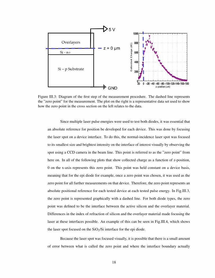
Figure III.3: Diagram of the first step of the measurement procedure. The dashed line representsthe ”zero point” for the measurement. The plot on the right is a representative data set used to showhow the zero point in the cross section on the left relates to the data.
Since multiple laser pulse energies were used to test both diodes, it was essential that
an absolute reference for position be developed for each device. This was done by focusing
the laser spot on a device interface. To do this, the normal-incidence laser spot was focused
to its smallest size and brightest intensity on the interface of interest visually by observing the
spot using a CCD camera in the beam line. This point is referred to as the ”zero point” from
here on. In all of the following plots that show collected charge as a function of z-position,
0 on the x-axis represents this zero point. This point was held constant on a device basis,
meaning that for the epi diode for example, once a zero point was chosen, it was used as the
zero point for all further measurements on that device. Therefore, the zero point represents an
absolute positional reference for each tested device at each tested pulse energy. In Fig.III.3,
the zero point is represented graphically with a dashed line. For both diode types, the zero
point was defined to be the interface between the active silicon and the overlayer material.
Differences in the index of refraction of silicon and the overlayer material made focusing the
laser at these interfaces possible. An example of this can be seen in Fig.III.4, which shows
the laser spot focused on the SiO2/Si interface for the epi diode.
Because the laser spot was focused visually, it is possible that there is a small amount
of error between what is called the zero point and where the interface boundary actually
18
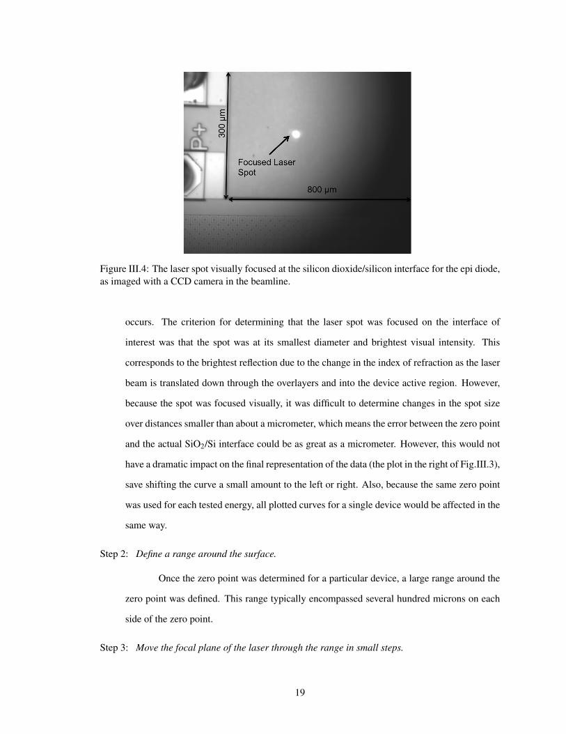
Figure III.4: The laser spot visually focused at the silicon dioxide/silicon interface for the epi diode,as imaged with a CCD camera in the beamline.
occurs. The criterion for determining that the laser spot was focused on the interface of
interest was that the spot was at its smallest diameter and brightest visual intensity. This
corresponds to the brightest reflection due to the change in the index of refraction as the laser
beam is translated down through the overlayers and into the device active region. However,
because the spot was focused visually, it was difficult to determine changes in the spot size
over distances smaller than about a micrometer, which means the error between the zero point
and the actual SiO2/Si interface could be as great as a micrometer. However, this would not
have a dramatic impact on the final representation of the data (the plot in the right of Fig.III.3),
save shifting the curve a small amount to the left or right. Also, because the same zero point
was used for each tested energy, all plotted curves for a single device would be affected in the
same way.
Step 2: Define a range around the surface.
Once the zero point was determined for a particular device, a large range around the
zero point was defined. This range typically encompassed several hundred microns on each
side of the zero point.
Step 3: Move the focal plane of the laser through the range in small steps.
19

After determining the zero point and defining a range of interest around the zero
point, the focal plane of the laser was placed on one of the boundaries of the range and moved
through it in small steps. The step size varied depending on which device was being tested
and the beam waist size used for the measurement. Typically, steps were on the order of
0.5-1.0 µm. Looking at the representative plot in Fig. III.3, the data points to the right of the
zero point are separated by more than 0.5-1.0 µm. Because the index of refraction of silicon
is 3.5 times that of air, the laser in the silicon actually moves 3.5 times farther than the step
taken by the linear stage on which the DUT is mounted. Therefore, a 1.0 µm step taken by
the stage results in a 3.5 µm step being taken by the portion of the beam within the silicon.
Step 4: Make a charge collection measurement at each step.
At each step, a charge collection measurement was made using the PHA methods
discussed earlier. Specifically, at each step, 300 pulses from the linear gain amplifier of the
PHA system were captured using a TDS6124C Digital Storage Oscilloscope and written out
to a file for processing later. The amplitudes of these pulses (which are proportional to the
amount of charge collected in the diode) were averaged at each position to produce a mean
collected charge at each position. For each output pulse recorded, a corresponding pulse
from the InGaAs photodiode was also recorded to keep a record of the laser pulse energy.
These pulses were averaged for the entire run. The reported laser pulse energies appearing in
the legends of the figures that follow are these averaged laser pulse energies. The standard
statistical error of each of the reported pulse energies is less than 5%.
Step 5: Create a plot of collected charge as a function of focal plane position.
The resulting data are plotted as collected charge as a function of laser pulse energy
and focal plane position in the DUT. The value on the y-axis represents the mean collected
charge at each position. Because the laser beam was normal to the surface of each tested
device, the position on the x-axis is referred to as the z-position; corresponding to movement
along the z-axis of the DUT. This assignment is arbitrary, but worth mentioning to avoid con-
fusion in the interpretation of the data. For all plots, values to the right of zero represent
moving the focal plane of the beam deeper into the device substrate. For the sake of conve-
nience, data plotted in this manner (collected charge versus z-position) will be referred to as
20

charge collection profiles for the remainder of this work.
21

CHAPTER IV
Impact of Beam Waist Diameter on Collected Charge
−180−160−140−120−100−80−60−40−200200
200
400
600
800
1000
z−position (µm)
Co
llec
ted
Ch
arg
e (
fC)
0.40 nJ
0.92 nJ
1.12 nJ
1.55 nJ
1.83 nJ
(a) Bulk Diode: 1.4 µm waist.
−600−500−400−300−200−1000800
200
400
600
800
1000
1200
z−position (µm)C
olle
cte
d C
ha
rge
(fC
)
2.1 nJ
3.5 nJ
5.6 nJ
7.0 nJ
(b) Bulk Diode: 7.0 µm waist.
Figure IV.1: Collected charge as a function of focal plane position and laser pulse energy for twodifferent beam waist diameters. Values to the right of zero on the x-axes represent moving the focalplane deeper into the substrates of the devices.
By changing the size of the focusing objective in the beamline, it was possible to investigate the
relationship between beam waist size and collected charge for the devices tested. (II.1) - (II.3) show
that critical properties of the beam are strongly dependent on the beam diameter at the waist. Earlier
calculations concerning the dependance of the TPA region on the beam waist diameter (see Fig. II.7)
show that the size of the beam waist diameter can have a dramatic impact on both the peak carrier
density and the vertical extent of the TPA region. However, because the TPA model presented here
neglects the higher order effects imposed by the optical processes involved in TPA-induced carrier
generation, making an attempt to verify the prediction of Fig. II.7, at least qualitatively, through
experimental measurements can provide valuable insight into the characteristics of the TPA region
inside an actual device.
Fig.IV.1 shows collected charge as a function of focal plane position for the bulk diode for two
different beam waist diameters. The laser pulse energies used for each run are noted in the plot
legends. It is apparent that the widths of the charge collection profiles are much greater for the 7.0
22
µm waist diameter. This is due to the confocal parameter of the beam as a result of the beam waist
diameter. The size of the confocal parameter of the beam depends on the beam waist diameter (see
(II.2)). The confocal parameter is a measure of the distance over which the beam is well collimated.
For the 1.4 µm waist diameter, the confocal parameter is approximately 9 µm. Because the confocal
parameter changes as a function of the beam waist diameter squared, the confocal parameter for the
7.0 µm beam waist is approximately 215 µm. Beyond the range of the confocal parameter, the
Gaussian beam profile starts to diverge rapidly, which significantly decreases the probability of
simultaneous photon absorption. Going back to the discussion of Section II.3, the larger confocal
parameter does indeed mean that for larger beam waist diameters, the TPA region becomes more like
a wide column of charge in the device, rather than a highly focused point-like carrier distribution.
Because of this, it is possible for charge to be collected a significant distance away from the focal
plane of the laser. For the bulk diode shown in Fig.IV.1b, this trend is apparent.
While both plots in Fig. IV.1 show approximately the same amount of peak collected charge
for the highest laser pulse energy, the laser pulse energies themselves are quite different. For the
1.4 µm waist, the laser pulse required to achieve the peak collected charge (1.83 nJ) is significantly
less than the pulse energy required to achieve a similar amount of charge collection with a 7.0 µm
waist diameter. This difference is even more striking when we recall that the total TPA-induced
carrier generation is proportional to the laser pulse energy squared. (II.3) describes the irradiance
of the beam in terms of the pulse power, radial distance from the z-axis, and, most relevant to
this discussion, the beam diameter. According to (II.3), for a 7.0 µm beam waist, the laser pulse
irradiance would be significantly less than that for a 1.4 µm beam waist. Because the irradiance is a
significant component of the TPA-induced carrier generation, described for the simple TPA model
by (II.6), a lower pulse irradiance due to a larger beam waist would lead to a lower peak carrier
density within the TPA region. So, for the same laser pulse energy at two different beam waist
diameters, the wider beam waist will lead to a lower carrier density, and thus a lower peak collected
charge.
There is also a significant difference in where the peak charge collection occurs for each beam
waist diameter. For the 1.4 µm waist, the peak collected charge occurs approximately 20 µm below
the zero point. For the 7.0 µm waist, the peak collected charge occurs much deeper in the device; at
approximately 150 µm away from the zero point. This is due to the vertical extent of the TPA region
23
for each beam waist size. The larger waist diameter leads to a much larger confocal parameter, and
thus a much larger TPA region. When the focal plane is at the zero point, a significant amount of
the carrier-generating region of the beam is contained in the overlayer material and the air above
the device. However, as the focal plane is moved deeper into the device substrate, more and more
of the carrier generating portion of the beam is moved into the device, resulting in increased carrier
generation and, thus, increased charge collection. This continues until the focal plane is so far
from the junction that the generated carriers from the high-density region around the focal plane of
the beam are too far away from the junction to be collected efficiently. A similar trend is seen in
Fig.IV.1a, however the charge peaks much closer to the zero point. This is because the TPA region
for the smaller waist diameter is much more tightly confined to the area around the focal plane of
the beam. This is a trend that will be discussed in more detail in the following chapter.
24
CHAPTER V
Laser Pulse Energy Trends
V.1 The Pulse Energy Dependence of the Charge Collection Profiles
−20 −10 0 10 20 30 40 50 60 700
5
10
15
20
25
30
35
40
z−position (µm)
Co
llec
ted
Ch
arg
e (
fC)
0.49 nJ
0.66 nJ
1.00 nJ
1.70 nJ
(a) Epi Diode: Low Energy Profiles
−20 −10 0 10 20 30 40 50 60 700
200
400
600
800
1000
1200
1400
z−position (µm)
Co
llec
ted
Ch
arg
e (
fC)
2.18 nJ
3.45 nJ
5.21 nJ
6.62 nJ
(b) Epi Diode: High Energy Profiles
Figure V.1: Collected charge as a function of laser pulse energy for the epi diode using a 1.4 µmbeam waist diameter. Values to the right of the zero point correspond to the focal plane being insidethe diode, while values to the left of zero correspond to the focal plane being outside the diode.Similar data for the bulk device is shown in Fig.IV.1.
Fig.V.1 shows charge collection profiles using the 1.4 µm waist diameter beam on the epi diode.
An arbitrary distinction has been made between low and high laser pulse energies to make discussion
of the plots more tractable. It should be noted, however, that what constitutes a low or high laser
pulse energy depends more on the device being tested than the actual numerical value of the pulse
energy. Effects such as shadowing of the active silicon by metal present in device overlayers, small
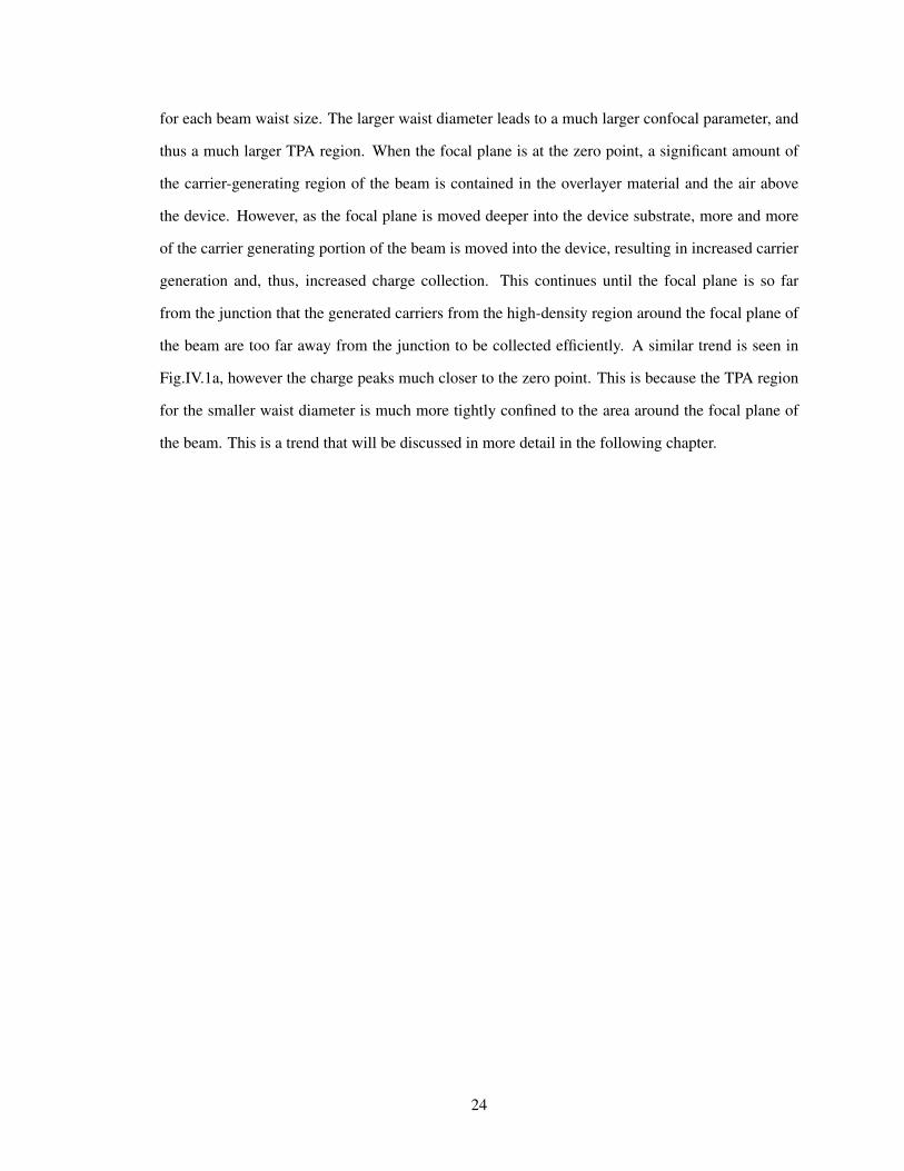
charge collection volumes, and others can have a significant impact on how much of the laser pulse
energy actually reaches the sensitive region of a device.
One trend present in Fig.V.1 is that for the low energy runs, the collected charge peaks at the
zero point defined for the device (the SiO2/Si interface), while for the higher energy runs, the peak
collected charge shifts off the surface by several micrometers. The reason for this shift at higher
energies is due to the TPA region itself. At the 1.4 µm waist diameter, the majority of the carriers
25
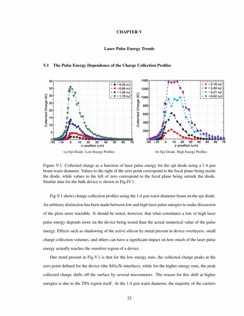
0 1 2 3 4 5 6 75
10
15
20
25
30
35
Pulse Energy (nJ)
FW
HM
(µ
m)
Figure V.2: The FWHM values of the charge collection profiles shown in Fig.V.1 for the epi diodeas a function of increasing laser pulse energy. The increasing FWHM shows that, as the laserpulse energy increases, the carrier density in the wings of the TPA region is able to contribute tomeasurable charge collection, even when the focal plane of the beam is deep in the device substrate.
within the TPA region are confined to the region surrounding the focal plane. However, as the laser
pulse energy increases, the carrier density of the entire TPA region increases as well. Therefore, not
only is the peak carrier density increasing, but also the carrier density away from the focal plane
of the beam. This is illustrated graphically in Fig. II.7. Though the pulse energy shown in that
figure is arbitrary, it does illustrate the trend that for increasing laser pulse energies, the ”wings” of
the TPA region can contain a significant amount of carriers. This means that measurable amounts
of collected charge will be observed at greater distances from the focal plane of the beam. Figs.
IV.1 and V.1 confirm this. For increasing laser pulse energies, the FWHM values of the charge
collection profiles increase. This increase is shown graphically in Fig.V.2. The figure shoes that
the charge collection profiles for higher laser pulse energies are wider than those for lower laser
pulse energies. This confirms that the carrier density in the wings of the TPA region can lead to
measurable charge collection, even when the high density portion of the charge cloud surrounding
the focal plane is well into the device substrate. This relates directly to the shift in peak collected
charge shown in Fig. V.1 for the high energy runs. As the pulse energy increases, the carrier density
in the wings of the TPA region becomes more significant. When the focal plane of the beam is at the
zero point, a portion of the beam capable of generating carriers is outside of the device. However,
similar to the discussion in the previous chapter concerning the 7.0 µm beam waist, as the focal
26
plane moves deeper in the device, the portion of the beam that was previously outside the silicon
enters the active region of the device and is capable of generating carriers that are collected by the
device. Eventually, as the laser pulse energy increases to a point where the carrier density in the
wings of the TPA region becomes significant, the peak collected charge will shift away from the
zero point (which is essentially the junction of the device).
Comparing the charge collection profiles of the bulk diode to those of the epi diode shows a
large discrepancy between the amount of charge collected in each device for similar laser pulse
energies. For example, Fig.IV.1a shows a peak collected charge of approximately 600 fC for a 1.55
nJ laser pulse. However, for the epi diode, a similar pulse energy of 1.70 nJ leads to a peak collected
charge of only 35 fC. Charge collection trends for epi versus bulk devices have been reported in the
literature many times for ion-induced charge collection [28, 29]. The presence of the highly doped
substrate in an epi device serves to truncate overall charge collection. For the epi diode, shifts in
the peak collected charge values are not seen until the 2.18 nJ run shown in Fig.V.1b, while, for the
bulk diode, peak shifts are seen at all tested laser pulse energies. The difference in substrate doping
is a contributing factor to the differences between the charge collection profiles for these devices.
For the two highest laser pulse energies for the epi diode, the charge collection profiles do not
have the well defined peaks present in all of the other charge collection profiles for the epi diode or
the bulk diode. In fact, for the 5.21 nJ and 6.62 nJ laser pulse energies, the charge collection profiles
flatten out considerably for a range of 15-20 µm from the zero-point. This not only violates the
analysis of (II.7), but suggests that for significantly high laser pulse energies, a region of constant
charge collection efficiency is formed in the device. No experimental work has been reported that
would verify this claim; however, a theoretical basis for this phenomenon has been discussed at
length by Edmonds [30–33]. According to that work, a point source of charge generation (to which
TPA is a reasonable approximation for small beam waist diameters) can produce a region of constant
charge collection efficiency in a silicon diode at sufficiently high generation rates. The focus of the
work of [31, 32] is on the development of an analytical model, called the Ambipolar Diffusion with
Cutoff (ADC) model, to describe high injection conditions in devices. While a full treatment of
the ADC model is well outside the scope of this work, these data will be included in a future work
seeking to experimentally verify the ADC model.
Fig.V.3 shows the peak collected charge as a function of laser pulse energy squared for both
27

0 10 20 30 40 500
0.2
0.4
0.6
0.8
1
1.2
1.4
1.6
Pulse Energy2 (nJ
2)
Co
llec
ted
Ch
arg
e (
pC
)
Data
Linear Fit
(a) Epi Diode
0 0.5 1 1.5 2 2.5 3 3.50
0.2
0.4
0.6
0.8
1
Pulse Energy2 (nJ
2)
Co
llec
ted
Ch
arg
e (
pC
)
Data
Linear Fit
(b) Bulk Diode
Figure V.3: Peak collected charge as a function of laser pulse energy squared for the plots shownin Fig.IV.1a and Fig.V.1. The pulse energy is squared to account for the dependence of the TPA-induced carrier density on laser pulse energy shown in (II.7).
diodes. The pulse energy is squared due to the square dependence the TPA-induced carrier density
has on laser pulse energy (see II.7). Squaring the pulse energy means the peak collected charge
should follow a linear trend. The dashed lines shown in Fig.V.3 represent a linear fit to the peak
collected charge values (black circles). For each fit, the R2 value was greater than 0.95, which
shows that the collected charge does indeed increase linearly as a function of the laser pulse energy
squared, as predicted by (II.7). While the fit is quite good for the bulk diode shown in Fig.V.3b, the
fit for the epi diode does show more variation from the trend line at the highest and lowest energies.
The over-prediction of the linear fit at the highest energy is due to the flattening out of the highest
energy charge collection profile. As was stated earlier, this is due to effects that are real, but outside
the scope of this work. It is unclear what is causing the linear fit to over-predict at the lowest laser
pulse energies for the epi diode. It is more than likely due to higher order optical effect that the TPA
model presented in this work does not take into account.
V.2 Comparison to Heavy Ion-induced Charge Collection
Because the ultimate goal of SEE laser testing is to gain insight into how a given device or circuit
would perform in a particle radiation environment, the comparison of heavy ion-induced collected
28
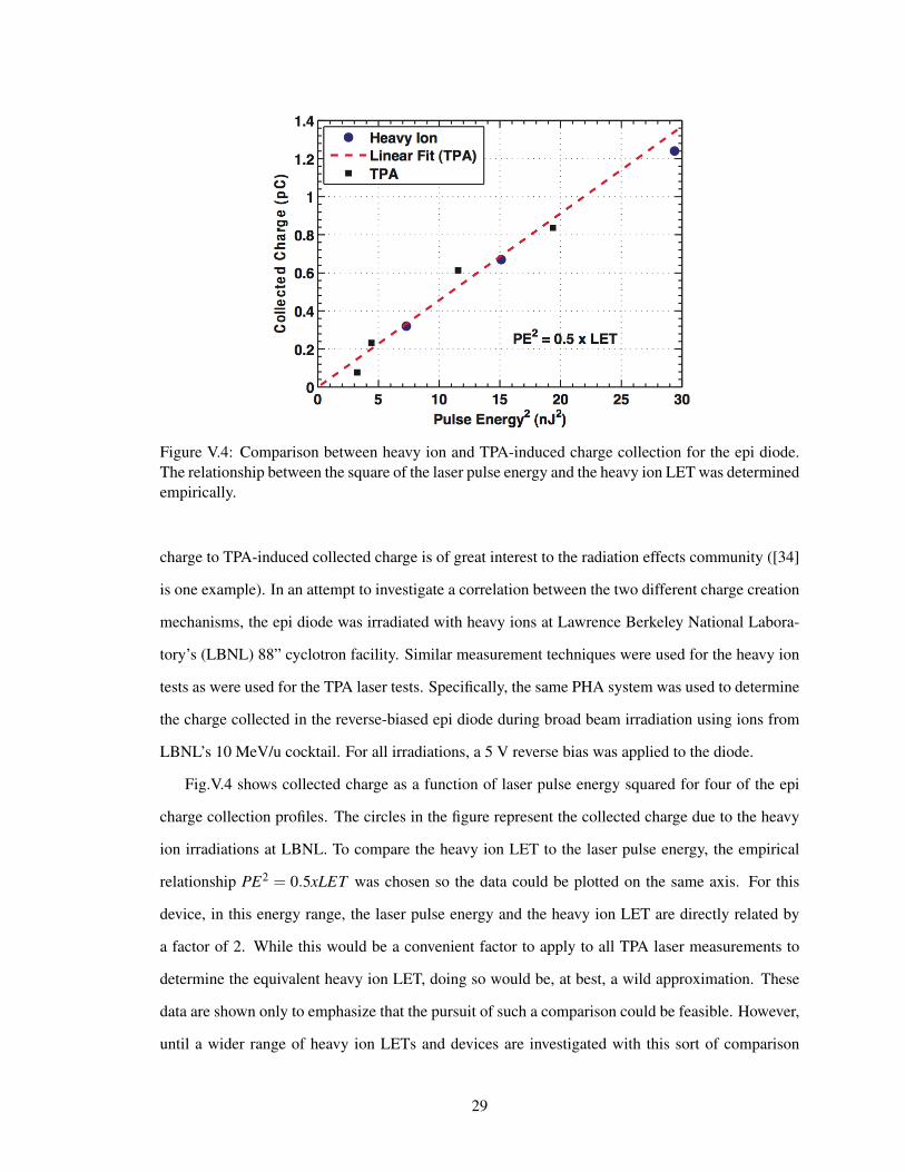
Figure V.4: Comparison between heavy ion and TPA-induced charge collection for the epi diode.The relationship between the square of the laser pulse energy and the heavy ion LET was determinedempirically.
charge to TPA-induced collected charge is of great interest to the radiation effects community ([34]
is one example). In an attempt to investigate a correlation between the two different charge creation
mechanisms, the epi diode was irradiated with heavy ions at Lawrence Berkeley National Labora-
tory’s (LBNL) 88” cyclotron facility. Similar measurement techniques were used for the heavy ion
tests as were used for the TPA laser tests. Specifically, the same PHA system was used to determine
the charge collected in the reverse-biased epi diode during broad beam irradiation using ions from
LBNL’s 10 MeV/u cocktail. For all irradiations, a 5 V reverse bias was applied to the diode.
Fig.V.4 shows collected charge as a function of laser pulse energy squared for four of the epi
charge collection profiles. The circles in the figure represent the collected charge due to the heavy
ion irradiations at LBNL. To compare the heavy ion LET to the laser pulse energy, the empirical
relationship PE2 = 0.5xLET was chosen so the data could be plotted on the same axis. For this
device, in this energy range, the laser pulse energy and the heavy ion LET are directly related by
a factor of 2. While this would be a convenient factor to apply to all TPA laser measurements to
determine the equivalent heavy ion LET, doing so would be, at best, a wild approximation. These
data are shown only to emphasize that the pursuit of such a comparison could be feasible. However,
until a wider range of heavy ion LETs and devices are investigated with this sort of comparison
29
in mind, this factor of 2 relationship between LET and laser pulse energy should be approached
with caution. However, because of the significance of such a relationship would have for future
SEE testing, it is worthwhile that these results, despite their preliminary nature, be shown here. A
detailed study of the relationship between heavy ion LET and TPA laser pulse energy in simple test
structures is the planned focus of future work.
30

CHAPTER VI
Comparing the Simple TPA Model to Experimental Results
While the simple TPA model is an approximation to the TPA-induced carrier density in an actual
semiconductor, it would be insightful to compare the charge collection due to a carrier distribution
described by the simple TPA model directly to the experimental results shown earlier. The sections
that follow discuss the implementation of the simple TPA model in two bulk silicon diode vari-
ants using Synopsys TCAD [35]. Specifically, two-dimensional TCAD models of the epi and bulk
diodes were created and the terminal currents as a function of time as a result of injecting a carrier
distribution similar to that shown in Fig.II.6 was recorded. The substrate doping for the simulated
epi diode was 5 x 1019 cm−3. The substrate doping of the simulated bulk diode was 5 x 1016 cm−3.
The results indicate that while the simple TPA model is useful for examining qualitative trends in
charge collection due to a TPA-induced carrier density, it is insufficient for a direct quantitative
comparison to the experimental data shown in previous sections.
VI.1 Simulation Specifics
All simulations were performed using the Sentaurus Device simulator from Synopsys. The
results presented here are the results of two-dimensional simulations of each diode’s response to a
TPA-induced carrier distribution. Because a thorough run of simulations that adequately reflected
the experimental measurements was required, cylindrical two-dimensional simulations were chosen
to keep simulation run-time at reasonable levels. The axis of revolution for the simulated device
corresponded to the longitudinal center of the TPA region, resulting in a carrier distribution with
cylindrical symmetry.
To determine the correct location and size for the contacts, a GDSII file containing information
about the layout of the diode was used. The doping profile of the epi diode was determined through
spreading resistance measurements. Fig.VI.1 shows the device geometry and doping profiles of the
epi diode. The bulk diode was identical, only its substrate doping was reduced to 5 x 1016 cm−3.
Fig.VI.1a shows the entire simulated structure, which was approximately 160 µm tall by 330 µm
wide. The width was determined directly from the GDSII file, while the height was chosen to
31

(a)
(b)
Figure VI.1: The two-dimensional epi diode as simulated in Sentaurus Device. Fig.VI.1a showsthe entire simulated diode while Fig.VI.1b shows only a portion of the diode consisting of the n+diffusion, p-epitaxial layer, and p+ substrate. The dark red region corresponds to silicon dioxide.Total doping concentration is plotted. The axes of each figure are in micrometers. The structure ofthe simulated bulk diode was identical, only the substrate doping matched that of the epitaxial layer.
32

allow as much of the TPA region as possible to be contained within the simulation space while still
maintaining a reasonable simulation run time.
The simulated device is contacted just as it is in the actual device. One contact runs along
the edge of the n+ diffusion. The p-epi layer is contacted similarly. The contacts can be seen in
Fig.VI.1b as purple lines on top of the epitaxial layer and n+ diffusions. Another contact runs along
the length of the bottom of the substrate. All contacts were made to be ideal in the simulator. For
all simulations, the device was biased identically to the experimental work discussed earlier. That
is, the p+ substrate and p-epitaxial layers were grounded while the n+ contacts were biased at 5 V.
At the full reverse bias, TCAD reported a depletion region width of 0.8 µm for the epi diode and
0.9 µm for the bulk diode.
TPA has been simulated in a device previously [20]. The simulations in this work use a similar
approach. Because the simulation software does not allow for computing the TPA-induced carrier
density through actual photon absorption processes, the TPA region must be defined as a carrier
distribution in the simulator. This is done by injecting a carrier distribution that looks identical to
that of Fig. II.6. By doing that, all of the approximations inherent to the simple TPA model are also
included in the simulations. While this does mean that quantitatively it would be very difficult to
compare experimental values for collected charge to the values produced by the simulator, it does
allow for the comparison and analysis of trends in the data in a qualitative sense. To accomplish
this in the simulator itself, an external library was written that calculates the TPA-induced carrier
density as a function of the parameters discussed earlier for the simple TPA model. This library is
dynamically linked to the simulator at run time to perform the required calculations.
The simulations were carried out in way that was very similar to the experiments discussed
earlier. The focal plane of the laser (which corresponds to the narrowest point in the carrier density
plot shown in Fig.II.6) was situated in the device, and the resulting carrier distribution simulated.
A series of these simulations was run with the focal plane at a different point in the device for each
simulation. Ultimately, what results is a plot of collected charge as a function of focal plane position
in the device, which is the same way the experimental data were presented.
For each simulation, a laser pulse energy of 0.25 nJ was used. Because the simulator does not
account for any affects that would cause a reduction in the amount of laser pulse energy that actually
contributes to creating the TPA region, even this seemingly small amount of laser pulse energy
33
injects quite a bit more carriers than is seen for similar energies during the experiment. Because
the simulations were cylindrical about the longitudinal axis of the TPA region, the actual amount
of carriers generated was π times the amount generated assuming a 0.25 nJ pulse. Therefore, the
actual amount of carriers generated during the simulations corresponds to a 0.78 nJ laser pulse.
A beam waist diameter of 1.4 µm was used in all simulations. Each simulation was run for 100
ns, which was enough time for all current transients to reach their asymptotic values. The carrier
recombination and generation physical models used by the simulator were the simple TPA model
discussed earlier, electron and hole avalanche models, and models for Auger and Shockley-Read-
Hall recombination. Other models included doping dependent carrier mobilities, carrier to carrier
scattering models, high field saturation models, OldSlotboom, Enormal, and a model to account for
Fermi statistics.
VI.2 Simulated Charge Collection Profiles
After all of the simulations were completed, it was possible to produce charge collection pro-
files similar to those seen in the previous chapters. This was done by numerically integrating the
terminal current as a function of time, which was recorded by the simulator. Fig. VI.2 shows charge
collection profiles for each of the simulated diodes. The simulation results show significantly more
charge collection than the experimental data shown earlier. Because of this, a simple calculation to
determine the amount of charge generated in the epitaxial layer of the epi device is beneficial for
determining if the simple TPA model was appropriately implemented in TCAD. To a rough approx-
imation, only carriers generated in the epitaxial layer will be collected. For the pulse energy used in
the simulations (0.78 nJ), the simple TPA model predicts a peak carrier density of 5 x 1018 cm−3.
Because the charge collection depth was determined through heavy ion experiments at LBNL, using
a charge collection depth of 2.1 µm in the calculation is reasonable. Also, because carrier genera-
tion is tightly confined within the 1.4 µm beam diameter, assuming a cylindrical charge collection
volume with a 0.7 µm radius is sufficient for a first order approximation of charge collection. Fi-
nally, assuming a 100% charge collection efficiency within the charge collection volume described
by the height and radius given above, multiplying the peak carrier density of 5 x 1018 cm−3 by
the charge of an electron produces a total generated charge of approximately 25 pC. Because this
calculation assumes a 100% efficient charge collection volume, that is also the amount of charge
34
collected by the epi device. This number is not drastically different than the peak charge collection
shown in Fig.VI.2 for the epi device, especially considering the approximate nature of the calcu-
lation. This suggests that the simple TPA model has been appropriately implemented in TCAD.
It does not, however, explain the discrepancy between the simulation results and the experimental
results shown earlier.
Part of the disagreement is due to the nature of the simple TPA model itself. A significant
amount of carriers are lost (or never even generated) during the TPA process due to the aforemen-
tioned higher order optical processes that the simple TPA model ignores. Because the simple model
does not take these optical effects into consideration, it assumes that 100% of the carriers that can be
generated by TPA are generated. This causes the simple TPA model to over-predict the amount of
carriers generated. This leads to an over-prediction in the amount of charge collected at the device
terminals.
Another possible culprit for the discrepancy between the simulation results and the measured
collected charge lies with the experiment itself. The pulse energies shown in the legends of Figs.
V.1 and IV.1 were measured in the beamline away from the DUT. It is possible that by the time the
beam reached the DUT, the pulse energy at the DUT was not the same as that back in the beam
line where the pulse energy measurement was made. This would lead to a significant discrepancy
between the collected charge measured during the experiment and that shown for the simulation
results. Attempting to identify and correct these sources of disagreement between the simulation
results and the results of the experiments is the focus of future work.
Regardless of the disagreement between the amount of charge collection seen in the experiments
and that reported by the simulations, several trends are present in Fig. VI.2 that can be seen in the
charge collection profiles shown earlier for both devices. For instance, for the epi diode, the peak
collected charge is considerably less than that of the bulk device. For the experimental data shown
in Figs. V.1 and IV.1a, which are for the epi diode and bulk diode respectively, the epi diode shows
less peak charge collection than the bulk diode for similar laser pulse energies. The main difference
between each of the diodes is their substrate doping concentrations, which is cause to believe that
the difference in substrate doping is a main factor contributing to the different peak values for the
experimental charge collection profiles, especially when the simulation results of Fig.VI.2 are taken
into account.
35
0 20 40 60 80 1000
5
10
15
20
z−position (µm)
Co
llec
ted
Ch
arg
e (
pC
)
Bulk
Epi
Figure VI.2: Simulated charge collection profiles for both diodes using a 0.25 nJ laser pulse and a1.4 µm waist diameter. Several trends are present in these data that can be seen in the experimentalcharge collection profiles shown earlier.
It has been shown both experimentally and in simulation that for ionizing particles, the presence
of an epitaxial layer over a highly doped substrate limits charge collection [28, 29]. A study focusing
on the differences in charge collection for a purely bulk diode versus one with a buried epitaxial layer
has not been previously discussed in the literature for a TPA-induced carrier distribution. However,
many of the same mechanisms are present for both doping cases. Chiefly, the presence of the highly
doped substrate limits the size of the charge collection volume in the device.
Another trend shown in Fig.VI.2 is that for decreasing substrate doping concentrations, the
charge collection profiles become wider. As the substrate doping decreases, two phenomena could
be leading to increased charge collection. For one, the carrier density in the wings of the TPA
could be dense enough at the lower substrate doping to cause greater amounts of charge collection.
Secondly, as the substrate doping decreases, carriers liberated deep in the substrate are able to
diffuse to the junction and be collected. As the doping decreases, the carrier lifetime (and thus
the carrier diffusion length) increases, allowing carriers to travel farther in the device before they
recombine. Because of this, the likelihood of a carrier liberated deep in the substrate diffusing to
the junction and being collected is greater in a lightly doped substrate. It is the interplay of both of
these phenomena that leads to the wider charge collection profile for the bulk diode. Also, for the
36

bulk device, there is a prominent shift in where the peak charge collection occurs. This suggests
that the wings of the TPA region are having a greater impact on charge collection for the bulk
diode. Because the collected charge peaks at the surface for the epi diode, the additional carriers
that are brought into the device as the focal plane moves deeper in to the substrate are not having as
noticeable an effect on the charge collection profile. This suggests that for the epi diode, only the
region of carrier generation directly around the focal plane of the laser is contributing to significant
charge collection.
37
CHAPTER VII
Implications for TPA SEE Testing
An interesting question is what these results, both experimental and from simulations, mean for
current TPA SEE testing methods. Two of the key observations from this work, the impact of the
beam waist diameter on overall charge collection and the shift in peak charge collection away from
the device junction for higher laser pulse energies and lower substrate dopings, do have important
implications for TPA SEE test methods.
Small changes in the beam waist diameter can lead to dramatic changes in overall collected
charge. This is shown in Figs. IV.1 and its accompanying discussion. Unexpected changes in the
beam waist diameter could make it very difficult to compare experimental results collected at differ-
ent times. Take, for example, (II.1)-(II.3), which describe how several important beam parameters
depend upon the beam waist diameter. Key among these is (II.3), which describes the pulse irra-
diance. The pulse irradiance depends strongly on the beam diameter. The equations governing the
TPA-induced carrier density, in turn, depend strongly on the pulse irradiance. Because of this, a
small change in the beam waist diameter over the course of several experiments (which might be
weeks or months apart) could lead to results that are difficult or impossible to interpret without a
detailed knowledge of the beam diameter. Measurements similar to those shown in Fig.III.2 taken
as a routine part of each experiment could help alleviate potential confusion, but would require sac-
rificing time that could be spent making other important measurements. Ultimately, if a particular
test campaign is expected to require many measurements over a long period of time, making a rou-
tine measurement of the beam profile could prove valuable when analyzing the experimental data.
This would help to account for any potential drifts or changes in the beam waist diameter over time.
It is possible that a large beam waist could be advantageous to some types of TPA SEE tests.
As shown in Fig.IV.1, a large beam waist gives rise to a large, columnar TPA region. In many TPA
experiments, it is desired to keep the TPA region as small as possible when testing small devices or
dense circuits. However, if it were desired to create a wide column of carriers in a device or circuit
and test its response to such a carrier distribution, increasing the beam waist diameter through the
use of different focusing objectives might be desirable. One particular example where this could be
38
useful is if the experimenter wants to examine the effects of multinode charge collection across a
large circuit area. Some TPA-induced latchup studies might also benefit from being able to inject a
large column of charge into a circuit.
Another possible testing concern is due to the peak shifts shown in Figs. IV.1a, V.1b, and VI.2.
These peak shifts may seem an innocuous side effect of TPA testing at first. However, when one
considers the methodology guiding a typical TPA SEE test, these peak shifts present cause for some
concern. In many TPA SEE tests, the laser spot is focused on the surface of the device and the focal
plane of the laser is moved along the z-axis until the largest charge collection is observed. Doing this
helps to ensure a favorable signal-to-noise ratio for the experiment. However, many TPA tests that
use this approach also assume that the greatest charge occurs when the focal plane is approximately
on the top surface of the device, which would correspond to injecting the most carriers directly
into the depletion region of the device. However, in making this assumption, experimenters also
assume that the spot size on the surface is that of the minimum beam waist diameter. As the results
presented here have shown, for sufficiently high laser pulse energies, or lightly doped substrates the
peak collected charge occurs when the focal plane of the laser is actually several microns below the
device surface. What this means is that the spot size on the surface could be several microns greater
than the beam waist diameter due to the rapid divergence of the profile of a Gaussian beam. For the
case of a TPA SEE test on dense SRAM, for example, this could mean that many more devices are
covered by the laser spot than would be covered if the narrowest portion of the beam were focused
on the surface of the device. This is a situation that can be remedied easily enough by focusing
the laser for a minimum spot size rather than maximum charge collection. This might reduce the
signal to noise ratio, but it would cause the spot size on the surface to be much closer to that of
the beam waist diameter. In some situations, measuring the greatest amount of charge collection is
the goal, rather than having precise knowledge of where in the device the majority of the carriers
are generated. If that is the case, the presence of peak shifts may not play a significant role in the
interpretation of the results.
In situations where charge collection from multiple adjacent devices is important, the presence
of peak shifts is a quality of TPA SEE testing that should not be overlooked. [36] discusses charge
collection from multiple devices due to parasitic bipolar amplification. While the charge collection
resulting from this effect is due to the interaction of several mechanisms, it is triggered by a pertur-
39

bation in the n-well potential due to ion strikes near the n-well boundary. Generating a sufficient
number of carriers near the n-well boundary can lead to a localized collapse of the n-well potential,
which triggers the effect. For TPA SEE testing, the reported peak shifts indicate that a significant
amount of carriers can be generated several microns below the top surface of the DUT when the
laser is focused for maximum charge collection. Depending on the experimental setup and the ge-
ometry of the DUT, this could place a significant amount of carriers around the n-well boundary,
which could lead to the unintentional triggering of the parasitic bipolar amplification effect.
40

CHAPTER VIII
Conclusions
The goal of this work has been to shed light on some of the more subtle aspects of TPA SEE
testing. A good understanding of the TPA effect requires a thorough understanding of the TPA
process and the role it can play in generating carriers in semiconductors. As such, background in-
formation was provided to develop a foundation of understanding for the remainder of the work.
Specifically, the equations governing the TPA process were discussed, as well as relevant Gaussian
beam parameters such as the confocal parameter and beam waist diameter. This led to the devel-
opment of a simple TPA model. This model ignores any higher order optical effects, which could
have a significant impact on the quantitative values for the TPA-induced carrier generation region in
an actual device. It does, however, serve as a good starting point to understand TPA in a qualitative
way. Any future modeling work concerning TPA in semiconductors will very likely begin with the
simple model before expanding to accommodate any higher order effects.
Following that, the experimental setup and methodology was discussed in some detail. This
involved a discussion of topics such as pulse height analysis, the geometry and dopings of the
devices to be tested, the determination of the beam waist diameter using the knife-edge technique,
and an explanation of the measurement procedure. The measurement procedure involved stepping
the focal plane of the laser through the device and making a charge collection measurement at each
step. The resulting collected charge was plotted as a function of position in the device. These plots
have been called charge collection profiles throughout this work.
The charge collection profiles for two different bulk silicon diodes were examined for two dif-
ferent beam waist diameters at a wide range of laser pulse energies. The profiles showed that for
increasing beam waist diameters, the TPA region becomes less like a localized region of carrier
generation and more like a wide column of charge in the device. It was also shown that at higher
laser pulse energies, the peak in collected charge occurred not when then focal plane of the device
was on the surface of the device (and thus approximately within the junction), but rather when the
focal plane was several microns below the surface. This was attributed to the wings of the TPA
region having a greater impact on charge collection at higher laser pulse energies.
41
The same trend was also observed as a function of doping. It was seen experimentally for the
two tested devices, one of which had a highly doped p-type substrate, while the other had a lightly
doped p-type substrate, and also observed in TCAD simulations of TPA. In the simulations, the epi
diode was modeled using cylindrical two-dimensional simulations. A series of simulations were
carried out in which the substrate doping was changed from a highly doped p-type to a lightly
doped p-type. The results of these simulations showed the trends seen in the experimental data.
That is, for a lighter doped substrate (i.e. the bulk diode), the peak in collected charge shifted off
of the surface for an identical laser pulse energy. There was a significant disagreement between
the amount of charge collected in the experiment, and the amount of collected charge from the
simulations. This discrepancy was attributed to the simplicity of the simple TPA model and the lack
of precise knowledge of the amount of laser energy reaching the DUT during the experiments. An
attempt to bring the simulation results and the measurements into better agreement will be the focus
of future work.
Finally, the implications of these results for TPA SEE testing were discussed. While none of
these results fundamentally alter the way that TPA SEE testing should be carried out, they do shed
light on some effects that should be taken into account when interpreting TPA SEE test data. Specif-
ically, the beam waist diameter should be monitored over the duration of long testing campaigns to
be sure that its size has not changed, which would make some results difficult to interpret. Also,
the impact of the aforementioned peak shifts in the presence of high laser pulse energies or a lightly
doped substrate should not be ignored, especially in test setups where the spot size of the laser at
the surface or charge collection from multiple adjacent devices is of a primary concern.
42
REFERENCES
[1]J. Melinger, S. Buchner, D. McMorrow, W. Stapor, T. Weatherford, A. Campbell, and H. Eisen,“Critical evaluation of the pulsed laser method for single event effects testing and fundamentalstudies,” IEEE Trans. Nucl. Sci., vol. 41, no. 6, pp. 2574 –2584, Dec. 1994.
[2]D. McMorrow, W. Lotshaw, J. Melinger, S. Buchner, and R. Pease, “Subbandgap laser-induced sin-gle event effects: carrier generation via two-photon absorption,” IEEE Trans. Nucl. Sci., vol. 49,no. 6, pp. 3002 – 3008, Dec. 2002.
[3]M. Gppert-Mayer, “ber elementarakte mit zwei quantensprngen,” Annalen der Physik, vol. 401,no. 3, pp. 273–294, 1931. [Online]. Available: http://dx.doi.org/10.1002/andp.19314010303
[4]A. Yariv, Quantum Electronics, 3rd ed. Wiley, Jan. 1989.
[5]J. Pellish, R. Reed, D. McMorrow, J. Melinger, P. Jenkins, A. Sutton, R. Diestelhorst, S. Phillips,J. Cressler, V. Pouget, N. Pate, J. Kozub, M. Mendenhall, R. Weller, R. Schrimpf, P. Marshall,A. Tipton, and G. Niu, “Laser-induced current transients in silicon-germanium hbts,” IEEE Trans.Nucl. Sci., vol. 55, no. 6, pp. 2936 –2942, 2008.
[6]D. McMorrow, S. Buchner, W. Lotshaw, J. Melinger, M. Maher, and M. Savage, “Demonstration ofsingle-event effects induced by through-wafer two-photon absorption,” IEEE Trans. Nucl. Sci.,vol. 51, no. 6, pp. 3553 – 3557, 2004.
[7]D. McMorrow, W. Lotshaw, J. Melinger, S. Buchner, Y. Boulghassoul, L. Massengill, and R. Pease,“Three-dimensional mapping of single-event effects using two photon absorption,” IEEE Trans.Nucl. Sci., vol. 50, no. 6, pp. 2199 – 2207, 2003.
[8]O. Amusan, B. Bhuva, M. Casey, M. Gadlage, D. McMorrow, J. Melinger, and L. Massengill, “Testcircuit for measuring single-event-induced charge sharing in deep-submicron technologies,” inMicroelectronic Test Structures (ICMTS), 2010 IEEE International Conference on, 2010, pp. 114–117.
[9]T. Loveless, L. Massengill, W. Holman, B. Bhuva, D. McMorrow, and J. Warner, “A generalizedlinear model for single event transient propagation in phase-locked loops,” IEEE Trans. Nucl.Sci., vol. 57, no. 5, pp. 2933 –2947, 2010.
[10]T. Loveless, L. Massengill, B. Bhuva, W. Holman, R. Reed, D. McMorrow, J. Melinger, and P. Jenk-ins, “A single-event-hardened phase-locked loop fabricated in 130 nm cmos,” IEEE Trans. Nucl.Sci., vol. 54, no. 6, pp. 2012 –2020, 2007.
[11]M. Casey, O. Amusan, S. Nation, T. Loveless, A. Balasubramanian, B. Bhuva, R. Reed, D. McMor-row, R. Weller, M. Alles, L. Massengill, J. Melinger, and B. Narasimham, “Single-event effectson combinational logic circuits operating at ultra-low power,” IEEE Trans. Nucl. Sci., vol. 55,no. 6, pp. 3342 –3346, 2008.
[12]J. Schwank, M. Shaneyfelt, D. McMorrow, V. Ferlet-Cavrois, P. Dodd, D. Heidel, P. Marshall,J. Pellish, K. LaBel, K. Rodbell, M. Hakey, R. Flores, S. Swanson, and S. Dalton, “Estimationof heavy-ion let thresholds in advanced soi ic technologies from two-photon absorption lasermeasurements,” IEEE Trans. Nucl. Sci., vol. 57, no. 4, pp. 1827 –1834, 2010.
43
[13]J. Schwank, M. Shaneyfelt, P. Dodd, D. McMorrow, G. Vizkelethy, V. Ferlet-Cavrois, P. Gouker,R. Flores, J. Stevens, S. Buchner, S. Dalton, and S. Swanson, “Direct comparison of charge col-lection in soi devices from single-photon and two-photon laser testing techniques,” IEEE Trans.Nucl. Sci., vol. 58, 2011 (to be published).
[14]A. Burnell, A. Chugg, and R. Harboe-S andrensen, “Laser sel sensitivity mapping of sram cells,”IEEE Trans. Nucl. Sci., vol. 57, no. 4, pp. 1973 –1977, 2010.
[15]D. McMorrow, S. Buchner, M. Baze, B. Bartholet, R. Katz, M. O’Bryan, C. Poivey, K. Label,R. Ladbury, M. Maher, and F. Sexton, “Laser-induced latchup screening and mitigation in cmosdevices,” in Radiation and Its Effects on Components and Systems, 2005. RADECS 2005. 8thEuropean Conference on, 2005, pp. C22–1 –C22–7.
[16]A. E. Siegman, Lasers. University Science Books, Jan. 1986.
[17]T. Boggess, K. Bohnert, K. Mansour, S. Moss, I. Boyd, and A. Smirl, “Simultaneous measure-ment of the two-photon coefficient and free-carrier cross section above the bandgap of crystallinesilicon,” Quantum Electronics, IEEE Journal of, vol. 22, no. 2, pp. 360 – 368, Feb. 1986.
[18]E. Van Stryland, H. Vanherzelle, M. A. Woodall, M. J. Soileau, A. L. Smirl, S. Guha, and T. F.Boggess, “Two photon absorption, non-linear refraction, and optical limiting,” Opt. Eng., vol. 24,pp. 613 – 623, 1985.
[19]R. W. Boyd, Nonlinear Optics, Third Edition, 3rd ed. Academic Press, Apr. 2008.
[20]A. Sternberg, Y. Boulghassoul, L. Massengill, D. McMorrow, W. Lotshaw, J. Melinger, S. Buchner,and R. Pease, “Three-dimensional modeling of the two photon absorption effect in a complexbipolar transistor,” in Radiation and Its Effects on Components and Systems, 2005. RADECS2005. 8th European Conference on, 2005, pp. PC22–1 –PC22–8.
[21]A. D. Bristow, N. Rotenberg, and H. M. van Driel, “Two-photon absorption and kerr coefficients ofsilicon for 850–2200 nm,” Applied Physics Letters, vol. 90, no. 19, p. 191104, 2007.
[22]W. T. Lotshaw, D. McMorrow, and J. S. Melinger, “Measurement of nonlinear absorption and re-fraction in doped si below the band edge,” in Nonlinear Optics: Materials, Fundamentals andApplications. Optical Society of America, 2007, p. WE10.
[23]M. Dinu, F. Quochi, and H. Garcia, “Third-order nonlinearities in silicon at telecom wavelengths,”Applied Physics Letters, vol. 82, no. 18, p. 2954, 2003.
[24]N. Dodds, “Charge generation by secondary particles from nuclear reactions in back end of linematerials,” Master’s thesis, Vanderbilt University, 1988.
[25]G. F. Knoll, Radiation Detection and Measurement, 3rd ed. Wiley, 2000.
[26]M. Clemens, N. Hooten, V. Ramachandran, N. Dodds, R. Weller, M. Mendenhall, R. Reed, P. Dodd,M. Shaneyfelt, J. Schwank, and E. Blackmore, “The effect of high-z materials on proton-inducedcharge collection,” IEEE Trans. Nucl. Sci., vol. 57, no. 6, pp. 3212 –3218, 2010.
[27]W. Shockley, “Problems related to p-n junctions in silicon,” Solid State Electron, vol. 2, pp. 35–67,1961.
[28]A. B. Campbell, A. R. Knudson, P. Shapiro, D. O. Patterson, and L. E. Seiberling, “Charge collec-tion in test structures,” IEEE Trans. Nucl. Sci., vol. 30, no. 6, pp. 4486 –4492, dec. 1983.
44
[29]H. Dussault, J. Howard, J.W., R. Block, M. Pinto, W. Stapor, and R. Knudson, “High energy heavy-ion-induced single event transients in epitaxial structures,” IEEE Trans. Nucl. Sci., vol. 41, no. 6,pp. 2018 –2025, dec 1994.
[30]L. Edmonds, “Electric currents through ion tracks in silicon devices,” Nuclear Science, IEEE Trans-actions on, vol. 45, no. 6, pp. 3153 –3164, dec 1998.
[31]——, “A proposed transient version of the adc charge-collection model tested against tcad,” NuclearScience, IEEE Transactions on, vol. 58, no. 1, pp. 296 –304, feb. 2011.
[32]——, “A theoretical analysis of steady-state charge collection in simple diodes under high-injectionconditions,” Nuclear Science, IEEE Transactions on, vol. 57, no. 2, pp. 818 –830, april 2010.
[33]——, “Charge collection from ion tracks in simple epi diodes,” Nuclear Science, IEEE Transactionson, vol. 44, no. 3, pp. 1448 –1463, jun 1997.
[34]J. Schwank, M. Shaneyfelt, D. McMorrow, V. Ferlet-Cavrois, P. Dodd, D. Heidel, P. Marshall,J. Pellish, K. LaBel, K. Rodbell, M. Hakey, R. Flores, S. Swanson, and S. Dalton, “Estimationof heavy-ion let thresholds in advanced soi ic technologies from two-photon absorption lasermeasurements,” Nuclear Science, IEEE Transactions on, vol. 57, no. 4, pp. 1827 –1834, aug.2010.
[35]Synopsys, “Sentaurus device,” http://www.synopsys.com/. [Online]. Available: http://www.synopsys.com/Tools/TCAD/DeviceSimulation/Pages/SentaurusDevice.aspx
[36]B. Olson, D. Ball, K. Warren, L. Massengill, N. Haddad, S. Doyle, and D. McMorrow, “Simultane-ous single event charge sharing and parasitic bipolar conduction in a highly-scaled sram design,”Nuclear Science, IEEE Transactions on, vol. 52, no. 6, pp. 2132 – 2136, dec. 2005.
45