fluorescence and raman measurements on gt-wrapped
TRANSCRIPT

Physics of Nanotubes, Graphite and Physics of Nanotubes, Graphite and Graphene Graphene
Mildred Dresselhaus Mildred Dresselhaus
Massachusetts Institute of Technology, Cambridge, MAMassachusetts Institute of Technology, Cambridge, MA
Quantum Transport and Dynamics in NanostructuresThe 4th Windsor Summer School on Condensed Matter Theory 6-18 August 2007, Great Park Windsor (UK)
Physics of Nanotubes, Graphite and Graphene
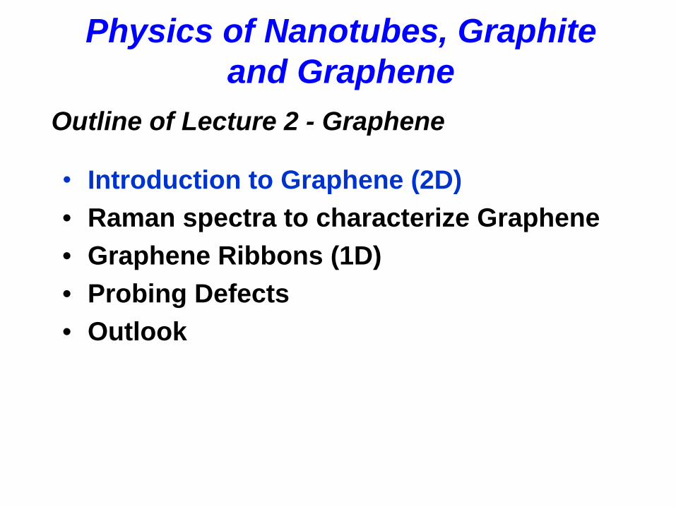
•
Introduction to Graphene (2D)• Raman spectra to characterize Graphene• Graphene Ribbons (1D)• Probing Defects• Outlook
Outline of Lecture 2 - Graphene
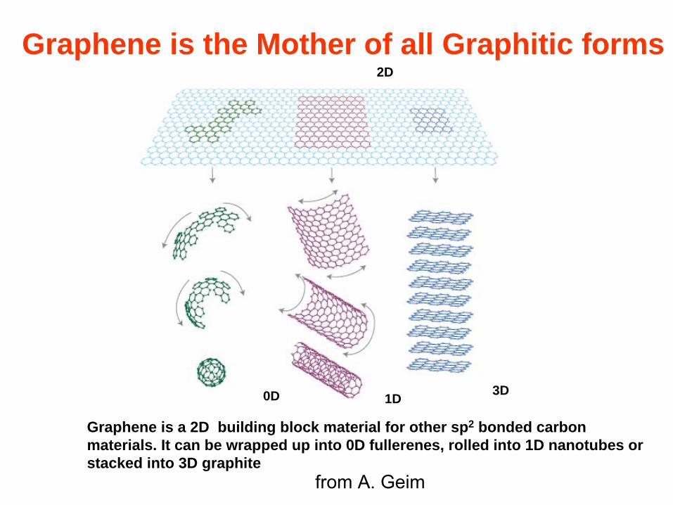
Graphene is the Mother of all Graphitic forms
Graphene is a 2D building block material for other sp2 bonded carbon materials. It can be wrapped up into 0D fullerenes, rolled into 1D nanotubes or stacked into 3D graphite
0D 3D1D
2D
from A. Geim

Identification of individual graphene sheets
•
1ML (monolayer) left, 2ML lower right•
Can be characterized by an optical microscope or by AFM, SEM and Raman
from Jing Kong, MIT

Graphene CrystalsOne atom thick single crystals
a)
Graphene visualized by atomic force microscope
b)
Graphene sheet freely suspended over posts
c)
Scanning electron micrograph of a relatively large graphene crystal showing armchair and zigzag edges. The edges of graphene crystals are of special importance because they are unique to few layer graphenes
and graphene ribbons
from A. Geim

Graphene devices•
Many graphene devices are similar to nanotube devices
•
Current Graphene technology:–
Mobility (~20000 cm2/Vs) can be further improved–
Ballistic transport on submicron scale–
Gas sensors to detect small gas concentrations•
A band gap can be opened by quantum confinement effects on armchair graphene ribbons
•
A band gap can be opened by placement of a graphene sample on a substrate, such as SiC
to form a weak
surface charge layer •
Spin polarization can be maintained over submicron distances
•
Interesting proximity effects are observed in graphene when using superconducting and magnetic electrodes
from Heersche, H. B., et al., Presented at Nanophysics: from Fundamentals to Applications, Hanoi, Vietnam, August, 2006

Carbon Valence Orbitals
•Strong in-plane sp2 (s,px ,py ) bonding•pz electrons form a nearly free electron gaswith E(k) linear in k

Electronic structure of Monolayer Graphene
Katsnelson, Mikhail I.
MATERIALS TODAY 10 (1-2):
Elsevier (2006)
•
E(k) relation is linear in k•
Effective mass vanishes at K and K'•
Different behavior from common metals and semiconductors because of linear instead of parabolic E(k) dispersion relation
armch
air edge
zigzag edge

Electronic Energy dispersion for GrapheneThe dispersion relation familiar from the graphene sheet that is
used to roll up graphene into a nanotube:
c-c3a a= ⋅where
and
(γ0
values are from 2.9 to 3.1eV)
Near the K point we write and
20
3( , ) 1 4 cos cos 4 cos2 2 2
y yxx y
k a k ak aE k k γ± = ± + +
is the transfer integral between nearest neighbor π-orbitals0γ
( ) v | |FE κ κ± = ± linear κ
relation where 03v2F
aγ=
k Kκ = −
and γ0
is the nearest neighbor overlap integral
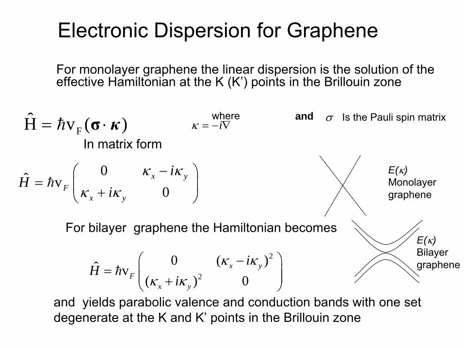
Electronic Dispersion for Graphene
For monolayer graphene the linear dispersion is the solution of the effective Hamiltonian at the K (K’) points in the Brillouin
zone
0ˆ v0
x yF
x y
iH
iκ κ
κ κ−⎛ ⎞
= ⎜ ⎟+⎝ ⎠
FH v ( )= ⋅σ κIn matrix form
For bilayer
graphene the Hamiltonian becomes
2
2
0 ( )ˆ v( ) 0
x yF
x y
iH
iκ κ
κ κ⎛ ⎞−
= ⎜ ⎟⎜ ⎟+⎝ ⎠
E(κ)Bilayergraphene
E(κ)Monolayer graphene
iκ = − ∇σwhere and Is the Pauli spin matrix
and yields parabolic valence and conduction bands with one set degenerate at the K and K’
points in the Brillouin
zone

AB stacking in Bilayer
GrapheneA-B-stackingA-A-stacking
•Theory is usually developed for AB stacking as in graphite.
•For bilayer
and multilayer graphene with randomly stacked layers we call the stacking turbostratic.
turbostratic

Graphite stacking

2D primitive cells of some Graphenes
Latil, Phys. Rev. Lett. 97, 036803 (2006)
Various stackings
up to 4 layer grapheneare shown

Electronic Band Structure of Monolayer and AB-stacked bilayer
Graphene
(a)
Monolayer graphene with linear E(k) near K point at EF(b)
Bilayer
AB stacked graphene E(k). The weak interaction between layers introduces a minigap
at the K point and parabolic bandsLatil, Phys. Rev. Lett. 97, 036803 (2006)Saito, Phys. Rev. B 33, 7218 (1986)

Ambipolar
Electric Field Effect
Ambipolar
electric field effect in single-layer graphene arising from the symmetry between valence and conduction bands. The insets show the low-energy spectrum E(k) as the Fermi level is raised by increasing the gate voltage Vg
from A. Geim

Minimum Conductivity of Graphene
The conductivity for different graphene samples indicates that the minimum conductivity is 4e2/h rather than
2e2/h as in typical semiconductors
from A. Geim

Anomalous Quantum Hall EffectThree anomalies: •
Half integer quantum Hall effect,
•
Factor of 4 in 4e2/h •
Berry’s phase of π
• This work attracted great attention and interest in graphene

Physics of Nanotubes, Graphite and Graphene
•
Introduction to Graphene (2D)• Raman spectra to characterize Graphene• Graphene Ribbons (1D)• Probing Defects• Outlook
Outline of Lecture 2 - Graphene

Comparison of the Raman spectra of graphene and graphite
ELaser =2.41eV
G’G’
G’A
G’B
•Large enhancement of G’
band in monolayer graphene relative to graphite•G’
band in monolayer graphene (and SWNTs) is a single peak, but the G’band for graphite has two components
J.C. Charlier,
P. C. Eklund, J. Zhu and A. C. Ferrari, vol
III, TAP, Springer

• Lespade et al., Carbon 22, 375 (1984).
•
Wilhelm
et al., Journal of Appl. Physics 84, 6552 (1998).
•
Nemanich
and Solin, Solid State Comm. 23, 417 (1977).
•
Nemanich
and Solin, Phys. Rev. B 20, 392
(1979).
•
Barros
et al., Phys. Rev. B 71, 165422 (2005).
Reason for G’-band NotationG’ band in the Raman spectra of 2D and 3D
graphites
Basis for the notation of theG’
band, comes from the graphite and nanographite
literature

Γ
K
Double resonance Raman scattering
K’K
, , ( )( )( )A B C i a i q b i q c
MI CE i E i E iω γ ω ω γ ω ω γ
=− − − − − − − −∑
Thomsen and Reich, Phys Rev Letters, 85, 5214 (2000)
Saito et al, Phys Rev. Letters, 88, 027401 (2002)
K

Double resonance Raman scattering
Γ K
)( kE
(a) (b)(c)
Intra-valley process: probing phonons near the Γ
point
Inter-valley process: probing phonons near the Κ
point
Thomsen and Reich, Phys. Rev. Letters 85, 5214 (2000)
°• •
•photon
defect
(a) (b) (c)photon
phonon
R. Saito, A. Jorio, A. G. Souza Filho, G. Dresselhaus, M.S. Dresselhaus, M.A. Pimenta, Phys. Rev. Letters, 588, 027401 (2002)
Intra-valley and inter-valley Double resonance

Double Resonance Stokes Process for Monolayer Graphene for the G′
feature
0'2 p GE ω=
J.C. Charlier,
P. C. Eklund, J. Zhu and A. C. Ferrari, vol
III, TAP, Springer
Use Saito notation
π
π∗
q
EF
Energy of scattered photon Esc is downshifted by relative tothe incident photon Ein
'in sc GE E ω= +
K’K
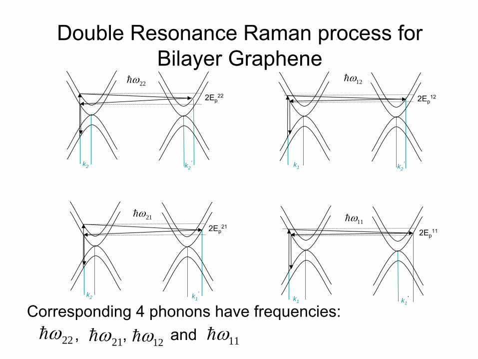
2Ep22
k2 k2’
2Ep12
k2’k1
2Ep21
k2 k1’
2Ep11
k1’
22ω 12ω
21ω11ω
Double Resonance Raman process for Bilayer
Graphene
Corresponding 4 phonons have frequencies:,
,
and 12ω21ω22ω 11ω
k1

G’1B G’1A G’2A G’2B
The four components of the G'
peak in bilayer
graphene
The lineshape
of G’
band identifies the number of layersThe relative intensities of the 4 peaks distinguishes bilayer
graphene from DWNTs
J.C. Charlier,
P. C. Eklund, J. Zhu and A. C. Ferrari, vol
III, TAP, Springer
Lineshape
is sensitive to both ELaser
and number of layers

Contrast G’
band in bilayer
graphene and DWNTs
at 2.41 eV
excitation
G’1B G’1A G’2A G’2B
Inte
nsity
(arb
. uni
ts)
•
Both bilayer
graphene (left) and double wall carbon nanotubes (right) have 4 peaks but the relative intensity of the peaks is different
•
Curvature effects and incommensurate interlayer structure strongly affect DWNTs
but are absent in bilayer
graphene.

G'
band for n=1-4. nLG
supported on SiO2
:Si for three laser excitation energies
J.C. Charlier,
P. C. Eklund, J. Zhu and A. C. Ferrari, vol
III, TAP, Springer
G’ G’ G’
•Because of the linear E(k) dispersion, ωG’
increases linearly with laser excitation energy
•Relative intensity of peaks change with Elaser

Dispersion of ωG’
with Elaser
for 1LG and 2LG
•
dωG’
/dElaser
~ 100 cm-1/eV in general•
The slope for p22
(or ω22’
) is steeper than for the others because of departures of E(k) from a linear k relation
L. Malard, M. Pimenta
(NT07)

G-band frequency vs. 1/n
-Spectra excited with 514.5 nm (2.41 eV) light and collected from nLGs
supported on a single SiO2
:Si substrate show small upshift
of 1LG graphene (5 cm-1) results
ELaser
=2.41eV
J.C. Charlier,
P. C. Eklund, J. Zhu and A. C. Ferrari, vol
III, TAP, Springer

G+G’
band for n=1-4. nLGs
on SiO2
:Si for two laser excitation energies
G+G’ G+G’
G+G’
feature is also sensitive to the number of graphene layers and also to Elaser
J.C. Charlier,
P. C. Eklund, J. Zhu and A. C. Ferrari, vol
III, TAP, Springer

Physics of Nanotubes, Graphite and Graphene
•
Introduction to Graphene (2D)• Raman spectra to characterize Graphene• Graphene Ribbons (1D)• Probing Defects• Outlook
Outline of Lecture 2 - Graphene
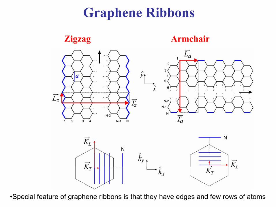
Graphene Ribbons
ArmchairZigzag
•Special feature of graphene ribbons is that they
have edges and few rows of atoms
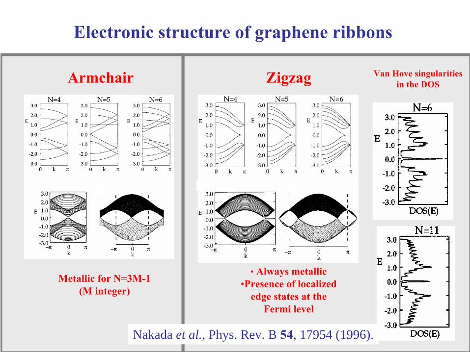
Electronic structure of graphene ribbons
Armchair Zigzag
Metallic for N=3M-1 (M integer)
• Always metallic•Presence of localized
edge states at the Fermi level
Van Hove singularities in the DOS
Nakada et al., Phys. Rev. B 54, 17954 (1996).
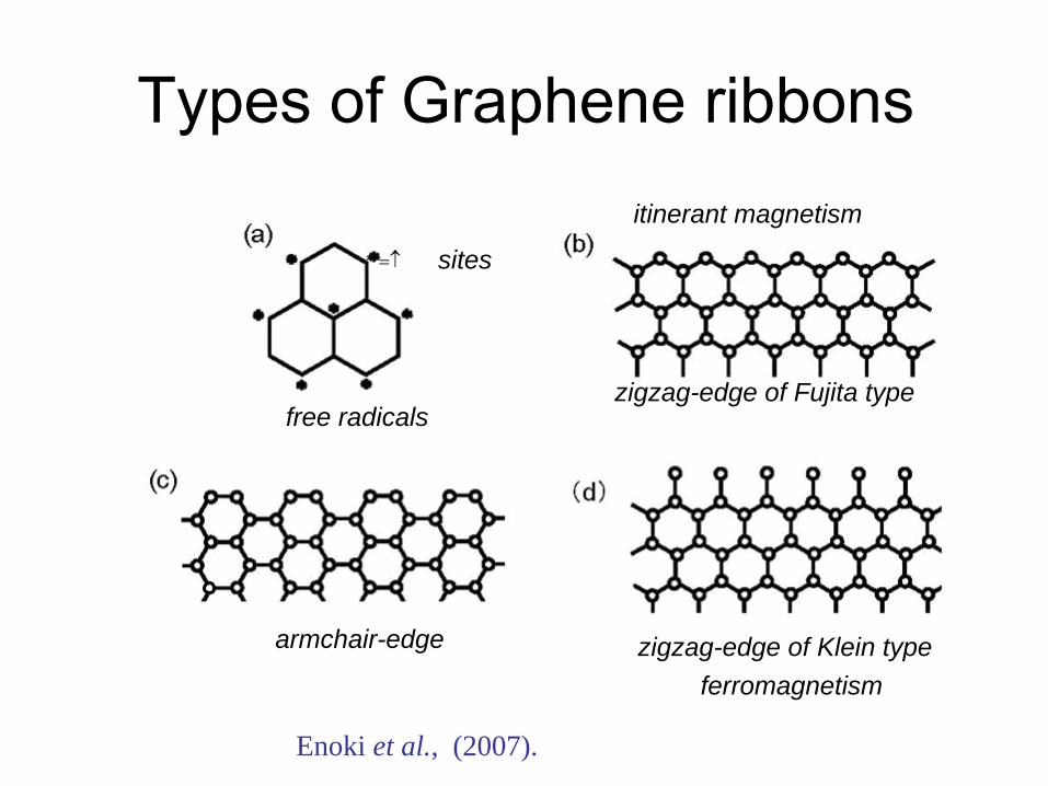
Types of Graphene ribbonsitinerant magnetism
sites* =↑
free radicalszigzag-edge of Fujita type
armchair-edge zigzag-edge of Klein typeferromagnetism
Enoki et al., (2007).

•
STM images of nanographenes
after heat treatment of nano-diamond particles at 1600°C. Magnified image on right
Affoune et al., Chem. Phys. Lett.
348, 17 (2001), Langmuir
17, 547 (2001) .

Spatial distribution of Population of HOMO level for nano-graphene
zigzag edges
•
Large Density of states is predicted at center of zigzag edges
armchair edges
Enoki et al., (2007).

Atomically-resolved UHV STM image of graphene edge
•
constant height mode STM image (Bias voltage 0.02V, I=0.1nA on 9x9nm2 sample)
•
dI/dVs
curve shows experimental evidence for high density of states for zigzag tubes
Enoki et al., (2007).

Graphene edge are armchair and zigzag edges
•
armchair edges are favored (more stable)

Raman and Scanning Probe Microscope studies in graphene edges
• The D-band intensity depends on the edge type
armchair edge
zigzag edge
• The D-band is more intense in armchair edges

•
The defect associated with the step edge is only able to transfer momentum in the direction perpendicular to the edge.
•
Raman spectroscopy can be used to distinguish between armchair and zig-zag edges.
L. G. Cançado, et al. Phys. Rev. Letters, vol. 93, 247401 (2004)
Double resonance Raman scattering in graphite edges

Graphene ribbons for Raman study
Synthesis: • Electrophoretic deposition of nano-diamond particles on a HOPG substrate.• At a temperature of 16000C, the nano-diamond particles are graphitized, forming nanographite sheets and ribbons.Affoune et al., Chem. Phys. Lett. 348, 17 (2001), Langmuir 17, 547 (2001) .
STM image of a zigzag ribbon:
AFM image of a monolayer graphene ribbon:
AFM image of many nanographite ribbons parallel to each other:
Cançado et al.,
Phys. Rev. Lett. 93, 047403 (2004).

Cançado et al., Phys. Rev. Lett. 93, 047403 (2004).
Raman spectra of graphene ribbons
Gruneis et al., Phys. Rev. B 67, 165402 (2003).
G1
- nanographite ribbonG2
- HOPG substrate

Physics of Nanotubes, Graphite and Graphene
•
Introduction to Graphene (2D)• Raman spectra to characterize Graphene• Graphene Ribbons (1D)• Probing Defects• Outlook
Outline of Lecture 2 - Graphene

First Order Raman spectra of nanographites

Optical
image
of HOPG deposited
on
glass
G band intensity
2μm
Performed by A..Jorio at Tuebingen Univesity, with A.Hartschuh

Confocal imaging of HOPG flakesG band imaging D band imaging
scan range 4 µm x 4 µm
D-band is emphasized at the edge

Dependence of the ratio ID / IG on the crystallite size (La ) in the Raman spectra of disordered graphite
Tuinstra and Koenig, J. Chem. Phys. 53, 1126 (1970).Tuinstra and Koenig, J. Compos. Mater 4, 492 (1970).
κ = 4.4 nm for λ = 514nm (2.41eV)
Knight and White, J. Mater. Res. 4, 385 (1989).
D G
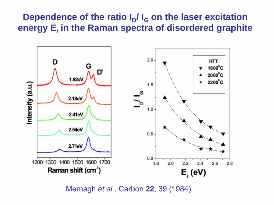
Dependence of the ratio ID / IG on the laser excitation energy El
in the Raman spectra of disordered graphite
Mernagh et al., Carbon 22, 39 (1984).

Γ
K
Double resonance Raman scattering
K’K
, , ( )( )( )A B C i a i q b i q c
MI CE i E i E iω γ ω ω γ ω ω γ
=− − − − − − − −∑
Thomsen and Reich, Phys Rev Letters, 85, 5214 (2000)
Saito et al, Phys Rev. Letters, 88, 027401 (2002)

Double resonance Raman scattering
Γ K
)( kE
(a) (b)(c)
Intra-valley process: probing phonons near the Γ
point
Inter-valley process: probing phonons near the Κ
point
Thomsen and Reich, Phys. Rev. Letters 85, 5214 (2000)
°• •
•photon
defect
(a) (b) (c)photon
phonon
R. Saito, A. Jorio, A. G. Souza Filho, G. Dresselhaus, M.S. Dresselhaus, M.A. Pimenta, Phys. Rev. Letters, 588, 027401 (2002)
Intra-valley and inter-valley Double resonance

Cançado et al., Applied Physics Letters
88, 163106 (2006).
General equation for the determination of the crystallite size
La of nanographite by Raman spectroscopy

General equation for the determination of the crystallite size
La of nanographite by Raman spectroscopy
Cançado et al., Applied Physics Letters
88, 163106 (2006).
Physics of Nanotubes, Graphite and Graphene
•
Introduction to Graphene (2D)• Raman spectra to characterize Graphene• Graphene Ribbons (1D)• Probing Defects• Outlook
Outline of Lecture 2 - Graphene

Outlook•
Nanostructured
carbon systems (fullerenes,
nanotubes, graphite) grow out of graphene.•
Graphene research is now expanding rapidly because of intrinsic interest with many new areas also opening up through suggestions from nanotubes, graphite, etc.
•
Carbon nanostructure fields are in various stages of development. This situation promotes cross stimulations between these fields to advance both science and applications