finfet doping : fabrication and metrology challenges · finfet doping : fabrication and metrology...
TRANSCRIPT

FINFET doping : fabrication and metrology challenges
W.Vandervorst
Imec, Belgium
Also : Inst. Kern- en stralingsfysika, KULeuven

Surname + NameIMEC confidential 2009 2
Why FINFET?
Chem. oxide
HfS
iO+
TiN
c-Si10 nm
Chem. oxide
HfS
iO+
TiN
c-Si10 nm)
c)
-0.5-0.4-0.3-0.2-0.1
00.10.20.30.40.5
20 40 60 80 100Lg (nm)
V T_s
at (V
)
Wfin = 17 nmWfin = 12 nmWfin = 8 nmWfin = 6 nm
pMOS
nMOS
Ioff
Ion
Gate
S D
Ioff
Ion
Gate
S D
Ioff
IonIoff
Ion
Gate
S D
Gate
S D
Ioff
Ion
Ioff
Ion
Gate
S DGate
S DTrigate
(Intel)
J. Kavalieros
et al., Symp. VLSI Tech. Dig. 2006.
FinFET (IBM, AMD, Freescale, NXP)
Presented at Frontie
rs on metro
logy for n
ano-electronics

Surname + NameIMEC confidential 2009 3
Conformal junctions in FINFET’s : 3D-profiling
buried oxide
Gate
uniform
Gate
Conformal(plasma, CVD?)
chan
nel
Gate
conformaltop rich
(tilted implants)
chan
nel
Gate
Top only(implant 0°)
chan
nel
Gate
uniform
Gate
uniform
Gate
Conformal(plasma, CVD?)
chan
nel
Gate
Conformal(plasma, CVD?)
chan
nel
Gate
conformaltop rich
(tilted implants)
chan
nel
Gate
conformaltop rich
(tilted implants)
chan
nel
Gate
Top only(implant 0°)
chan
nel
Gate
Top only(implant 0°)
chan
nel
Hardmask
0.0 0.2 0.4 0.6 0.8 1.01E-10
1E-9
1E-8
1E-7
1E-6
1E-5
1E-4
1E-3
I (dr
ain)
(Am
ps)
V(gate) (Volts)
Conformal Top Only
B
B’Tilted top view
Gate
Fin
Tilted top view
Gate
Fin
40nm gate16nm
fin
60 nm60 nm60 nm
Si
NiSi
NiSi NiSi
High-k + MG
poly-Si
Buried oxide
20 nm
S/D
Gate
Presented at Frontie
rs on metro
logy for n
ano-electronics

Surname + NameIMEC confidential 2009 4
S/D Junction formation requirements
• Junction conformality/uniformityGate
Source Drain
extensio
ns
extensio
ns
spacer spacerTop:high dose
Side:low dose
currentcurrent
SCE controlSCE control
B
Silicon BOX
Gate+ HMSpacer
Silicide
B’
B
Silicon BOX
Gate+ HMSpacer
Silicide
B’
FIN resistance : high doping, overlap
0° 10° 45°0° 10° 45°
Ionn
Ioff
Increased sidewall doping
Presented at Frontie
rs on metro
logy for n
ano-electronics
Surname + NameIMEC confidential 2009 5
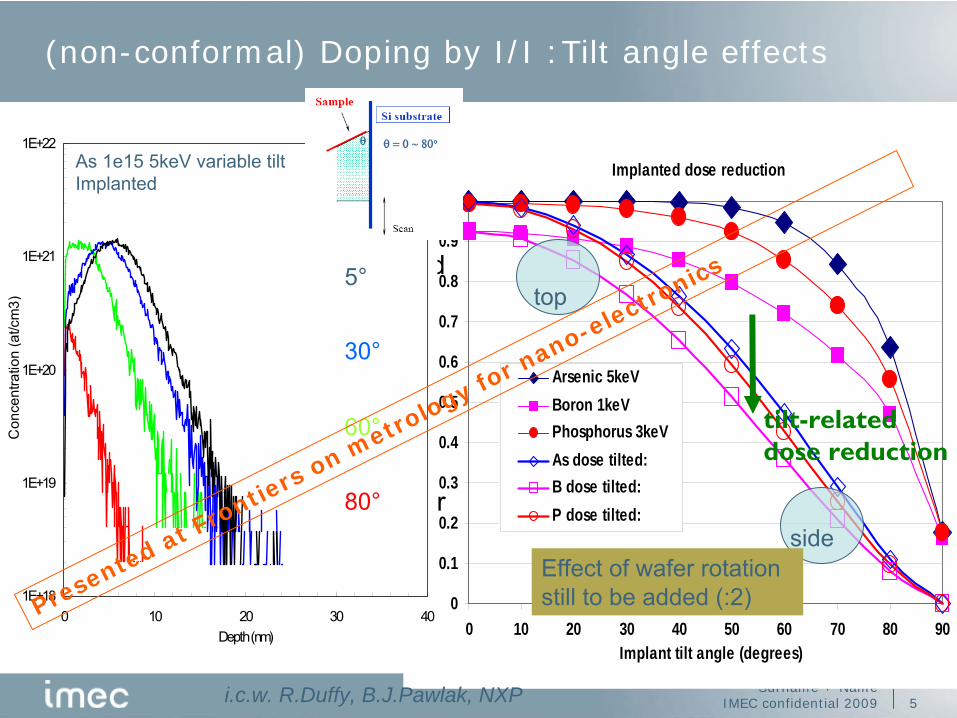
0
0.2
0.4
0.6
0.8
1
1.2
0 10 20 30 40 50 60 70 80 90
implant angle
rela
tive
dose
As 5 kev
P 3 keV
B 1 keV
500 eV B
200 eV B
(non-conformal) Doping by I/I :Tilt angle effects
Θ°backscattering and sputtering (SRIM 2003)
side
top
Implanted dose reduction
0
0.1
0.2
0.3
0.4
0.5
0.6
0.7
0.8
0.9
1
0 10 20 30 40 50 60 70 80 90Implant tilt angle (degrees)
Frac
tion
of th
e re
tain
ed d
ose
Arsenic 5keVBoron 1keVPhosphorus 3keVAs dose tilted:B dose tilted:P dose tilted:
tilt-relateddose reduction
Taperededge
Irregularedge
Reflection at surface
Back-
scatteri
ng
Target sputtering
BOX
Tilt angle
top
side
i.c.w. R.Duffy, B.J.Pawlak, NXP
Effect of wafer rotation still to be added (:2)
Buried Oxide
SiSiSiSiSi
Resist
NMOSNMOS PMOSPMOS
10-20°
70-80°to side
Buried Oxide
SiSiSiSiSi
Resist
NMOSNMOS PMOSPMOS
10-20°
70-80°to side
1E+18
1E+19
1E+20
1E+21
1E+22
0 10 20 30 40Depth (nm)
Con
cent
ratio
n (a
t/cm
3)
5°
30°
60°
80°
As 1e15 5keV variable tiltImplanted
Presented at Frontie
rs on metro
logy for n
ano-electronics

Surname + NameIMEC confidential 2009 6
Junction parameters : Planar vs FINFET
•Rs
•Xj
•(Vertical)
•Lateral
•Steepness
•Lateral
•Conformality
•Metrology
•2D
•3D
•Rs
•Xj
•Vertical
•Lateral
•Steepness
•Lateral
•Metrology
•1D (Rs, SIMS)
•2D (SSRM)
PLANAR FINFET
buried oxide
Presented at Frontie
rs on metro
logy for n
ano-electronics

Surname + NameIMEC confidential 2009 7
FINFET’s conformal doping and its metrology
Conformal doping• Implantation
– Tilt angle and incorporation efficiency
– Shadowing in dense structures (< 10-20° tilt)
– Amorphization and recrystallization
• Plasma immersion– Conformality ??
– Incorporation versus erosion
• VPD– Integration
– Outdiffusion
Properties Rs vs Xj has no meaning! Lateral profiles, sidewall dose, conformality
Metrology•SIMS through FINs•Resistors•S/D area’s : X-SSRM•3D-SSRM•3D-Atomprobe
Presented at Frontie
rs on metro
logy for n
ano-electronics

Surname + NameIMEC confidential 2009 8
SIMS through FINs
SIMS conc.
Dep
th
Poly-Si
Si
Si Si Si Si Si Si
Poly-Si
Si
Si Si Si Si Si Si
total SIMS craterN Concentration H −= ×Δtotal SIMS crater SIMS crater SIMS craterN Concentration H B W− − −= ×Δ × ×
total fin SIMS crater SIMS craterN No. of fins in SIMS crater D H B− −= × ×Δ ×
fin finD Concentration P= ×Presented at Frontie
rs on metro
logy for n
ano-electronics

Surname + NameIMEC confidential 2009 9
SIMS results
Sidewall Dose retention
Implants at 5keV 45° tilt 10° tiltSidewall dose
retention Ratio(45° vs. 10 °)
Arsenic 1 x 10¹⁵ /cm2 1.06 x 10¹⁵ /cm2 2.20 x 10¹⁴ /cm2 4.83
BF2 8 x 10¹⁴ /cm2 5.74 x 10¹⁴ /cm2 1.38 x 10¹⁵ /cm2 4.18
• BF2 5keV 8e14 at 45° and 10°• As 5keV 1e15 at 45° and 10°
• RTA annealed at 1050°C
Array of 10 fins
Deposited Si
200nm
80nm 200nm
Array of 10 fins
Deposited Si
200nm
80nm 200nm
Presented at Frontie
rs on metro
logy for n
ano-electronics

Surname + NameIMEC confidential 2009 10
Sidewall doping by I/I :SIMS vs theory
W.Vandervorst et al. , J. Vac. Sci. Technol. B 26 (1), Jan/Feb 2008, 396-401
Includes effect of 2 quad. implant
Presented at Frontie
rs on metro
logy for n
ano-electronics
Surname + NameIMEC confidential 2009 11
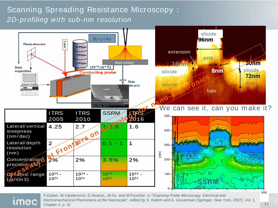
Scanning Spreading Resistance Microscopy : 2D-profiling with sub-nm resolution
SSRM
R=ρ/4a
Conducting probe
bias(50-500 mV)
to ADC
(10 -10-12 -4Α)
Log Amp
metal
diamond
metal
diamond
Back contact
R=ρ/4a
Conducting probe
bias(50-500 mV)
to ADC
(10 -10-12 -4Α)
Log Amp
bias(50-500 mV)
bias(50-500 mV)
to ADC
(10 -10-12 -4Α)(10 -10-12 -4Α)-12 -4Α)
Log Amp
metal
diamond
metal
diamond
Back contactBack contact
1014 -1021
1015 -1021
1014 -1021
1014 -1021
Dynamic range (at/cm3)
2%3-5%2%2%Concentration precision (%)
10.5 - 122Lateral/depth resolution (nm)
1.61-1.52.74.25Lateral/vertical steepness (nm/dec)
ITRS 2016
SSRMITRS 2010
ITRS 2005
1014 -1021
1015 -1021
1014 -1021
1014 -1021
Dynamic range (at/cm3)
2%3-5%2%2%Concentration precision (%)
10.5 - 122Lateral/depth resolution (nm)
1.61-1.52.74.25Lateral/vertical steepness (nm/dec)
ITRS 2016
SSRMITRS 2010
ITRS 2005
P.Eyben, W.Vandervorst, D.Alvarez,, M.Xu. and M.Fouchier, in “Scanning Probe Microscopy, Electrical and Electromechanical Phenomena at the Nanoscale”, edited by S. Kalinin and A. Gruverman (Springer, New York, 2007), Vol. 1, Chapter 2, p. 31
96nm
8nm72nm
30nm16nm
96nm
8nm72nm
30nm16nm
96nm
8nm72nm
30nm16nmsilicide
source
silicide
drain
silicide
gateextension
halo
We can see it, can you make it?
Presented at Frontie
rs on metro
logy for n
ano-electronics

Surname + NameIMEC confidential 2009 12
SSRM (FIN-like) applicationsΩ
ONO layer
Si FinPoly
1010 Ω
1012 Ω
Inversion layer, corner effect
1010 Ω
1012 Ω
1010 Ω
1012 Ω
1010 Ω
1012 Ω
Inversion layer, corner effect
M.Specht, D.Alvarez
S.Kluth et al.
Presented at Frontie
rs on metro
logy for n
ano-electronics

Surname + NameIMEC confidential 2009 13
SSRM on FIN : As I/I
Arsenic ImplantImplant
angleTop Sidewall Theoretical
45° 28nm 24nm 28nm
10° 35nm 18nm 6nm
( )sidewall top surfaceDepth tan Depthα −= ×Array of 10 fins
Deposited Si
200nm
80nm 200nm
Array of 10 fins
Deposited Si
200nm
80nm 200nm
Presented at Frontie
rs on metro
logy for n
ano-electronics
J.Mody et al, Insight-2009
Surname + NameIMEC confidential 2009 14
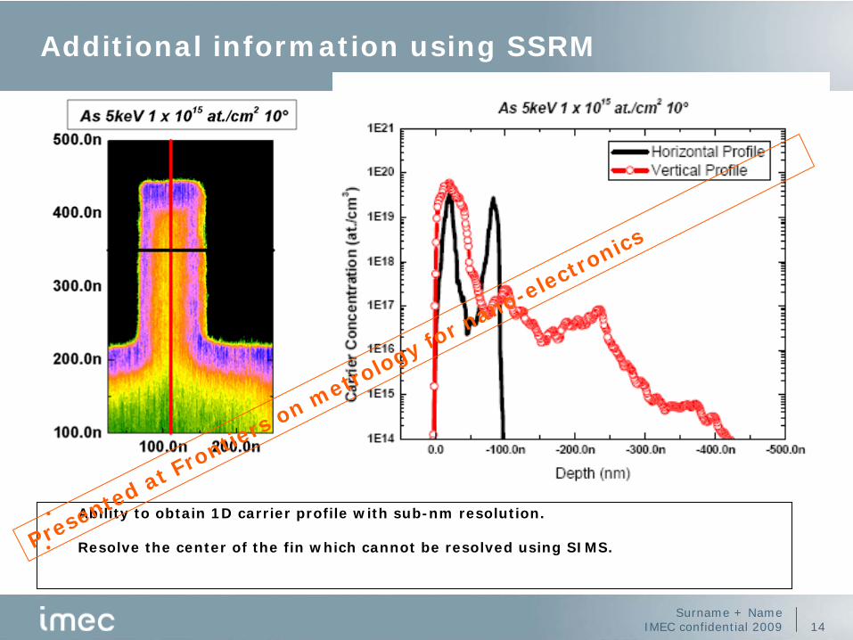
Additional information using SSRM
• Ability to obtain 1D carrier profile with sub-nm resolution.
• Resolve the center of the fin which cannot be resolved using SIMS.Presented at Frontie
rs on metro
logy for n
ano-electronics

Surname + NameIMEC confidential 2009 15
SSRM on FIN : BF2 I/I
BF2 Implant
Implantangle
Top Sidewall Theoretical
45° 35nm 31nm 35nm
10° 36nm 15nm 7nm
( )sidewall top surfaceDepth tan Depthα −= ×
Presented at Frontie
rs on metro
logy for n
ano-electronics

Surname + NameIMEC confidential 2009 16
Comparison SIMS-SSRM
ImplantSIMS Sidewall Ratio
(45° vs. 10°)SSRM Sidewall Ratio
(45° vs. 10°)
Arsenic 4.83 3.42
ImplantSIMS/SSRM Sidewall
Ratio 10°
SIMS/SSRM Sidewall Ratio 45°
Arsenic 0.95 1.33Presented at F
rontiers on m
etrology fo
r nano-electro
nics

Surname + NameIMEC confidential 2009 17
Summary of sidewall doping : As
Single sidewall dose Implant Dose sin( ) cos( ) incorporation efficiency ( )α α α= × ×
J. Vac. Sci. Technol. B 26 (1), Jan/Feb 2008, 396-401
fin finD Concentration P( ) / 2= ×
Presented at Frontie
rs on metro
logy for n
ano-electronics

Surname + NameIMEC confidential 2009 18
Comparison SIMS-SSRM
ImplantSIMS Sidewall Ratio
(45° vs. 10°)SSRM Sidewall Ratio
(45° vs. 10°)
BF2 4.18 9.79
ImplantSIMS/SSRM Sidewall
Ratio 10°
SIMS/SSRM Sidewall Ratio 45°
BF2 1.52 0.63Presented at F
rontiers on m
etrology fo
r nano-electro
nics

Surname + NameIMEC confidential 2009 19
Summary of sidewall doping : BF2
Single sidewall dose Implant Dose sin( ) cos( ) incorporation efficiency ( )α α α= × ×
• Good correlation between theoretical model, SIMS and SSRM
J. Vac. Sci. Technol. B 26 (1), Jan/Feb 2008, 396-401
fin finD Concentration P( ) / 2= ×
Presented at Frontie
rs on metro
logy for n
ano-electronics

Surname + NameIMEC confidential 2009 20
1D-profiles (and 1D-tuning) are meaningless
1.E+18
1.E+19
1.E+20
1.E+21
1.E+22
1.E+23
0 10 20 30 40 50 60 70 80 90
depth (nm)
Con
cent
ratio
n(a
t/cm
3
1.2K/25 sec
1.7 K/25 sec
1.7 K/200W/25 sec
1.7K/150/50(Ar). 25 sec eq
1.7K/50/150 (Ar),25 sec eq
1.7K/5.8/100 sec
elec. Active
Dose(atm/cm2)
2.47E152.52E152.51E154.98E15
Rs(Ω/cm2)
457457
-446
Similar 1D-profiles give very different conformality!!!
d07
-b2h
6
Presented at Frontie
rs on metro
logy for n
ano-electronics

Surname + NameIMEC confidential 2009 21
Resistor methodology
Hard mask protecting top of FIN
Implant or Plasma
BOX
FIN
HM
Pseudo VDP- or 2PP measurement
Poly-Si Fin,high diffusion!
RFin ~ 1/N
Full silicidation of unprotected area.
W.Vandervorst et al. JVST (2008)
BF3 P3I
W03 W04 W05 W06 W07 W08 W09 W10
200
400
600
800
1000
1200
2_po
int_
resi
stan
ce/R
2vf
wafer
BF3 P3I
W03 W04 W05 W06 W07 W08 W09 W10
200
400
600
800
1000
1200
2_po
int_
resi
stan
ce/R
2vf
wafer
Presented at Frontie
rs on metro
logy for n
ano-electronics

Surname + NameIMEC confidential 2009 22
Metrology for conformality
• SIMS through FIN’s : – Dopants,not active carriers
– No details on lateral junctions depths
– No wafer mapping
• Scanning Spreading Resistance Microcopy (SSRM) on cross sections of S/D fin’s
– Active carriers, real Xlat numbers
– No wafer mapping
• Resistors (R ~ 1/Sidewall dose)
– Relative
– Wafer mapping
P.Eyben, Vandervorst W. et al. . “Scanning Probe Microscopy : Electrical and Electromechanical Phenomena at the Nanoscale. Chapter II:SSRM, pp.31-87 (2007) (Springer).
R.Duffy et al., MRS -2008, J.Mody, Insight- 2009
W.Vandervorst et al., Proc. INSIGHT-2007, JVST B (2008)
Presented at Frontie
rs on metro
logy for n
ano-electronics
Surname + NameIMEC confidential 2009 23
plasma doping :Concurrent doping and erosion.
1.E+02
1.E+03
1.E+04
1.E+05
1.E+06
1.E+07
1.E+08
0 50 100 150 200norm. BF3-dose
RFI
N
150/50
50/150
previous, 100/50, 100/100
100 Bf3
HM after RTA< Ar-dilution
W.Vandervorst, IIT-2008
6 .0x10 -7
7 .0x10 -7
8 .0x10 -7
9 .0x10 -7
4 .0x10 -7 5 .0x10 -7 6 .0x10 -7 7 .0x10 -7
SSRM : Conformal!
1.00E+03
1.00E+04
1.00E+05
1.00E+06
1.00E+07
0 50 100 150 200
Depth (nm)Sp
read
ing
Res
ista
nce
(ohm
s)
D06 vert inD06 vert out
D06 lat in
1.E+02
1.E+03
1.E+04
1.E+05
0 0.5 1 1.5 2Vbias (KV)
RFI
N (O
hm)
0
1
10
100
HM
-ero
sion
(nm
)
source 200 Wsource 1000 WBF3 + B2H6no HMErosionErosion 1000W
lack of conformality
1.E+02
1.E+03
1.E+04
1.E+05
0 0.5 1 1.5 2Vbias (KV)
RFI
N (O
hm)
0
1
10
100
HM
-ero
sion
(nm
)
source 200 Wsource 1000 WBF3 + B2H6no HMErosionErosion 1000W
lack of conformality
Presented at Frontie
rs on metro
logy for n
ano-electronics

Surname + NameIMEC confidential 2009 24
3D-metrology
•Carriers : 3D-SSRM : Slice and view
•DopantsTomographic atomprobe
Presented at Frontie
rs on metro
logy for n
ano-electronics

Surname + NameIMEC confidential 2009 25
3D-profile in FinFET : SSRM slice and view
j.mody, mrs 2008S/D
Gate
Presented at Frontie
rs on metro
logy for n
ano-electronics

Surname + NameIMEC confidential 2009 26
Practical Problems
G
B
B’
A
A’
C
C’
G
B
B’
A
A’
C
C’
• To obtain 3D-profile we must obtain successive 2D-spreading resistance maps in one of the planes with 1nm step.
• Polishing ??? • Cleaving ???
• Cleaving and polishing with nanometer step in the planes ???
• Successive cleaving with 1nm step on the same transistor ???• Successive polishing with 1nm step on the same transistor ???
Presented at Frontie
rs on metro
logy for n
ano-electronics

Surname + NameIMEC confidential 2009 27
3D SSRM : slice and view
1 nm
Presented at Frontie
rs on metro
logy for n
ano-electronics

Surname + NameIMEC confidential 2009 28
3D-SSRM :proof of concept
100 150 200 250 300 350 400 450 500
105
106
Error bar = Average Reproducibility = 18%
Res
ista
nce
(Ohm
s)
Length (nm)
Average resistance (Fin 1 - Fin 8)
FinSubstrate
J.Mody et al., MRS-Spring 2008
0 100 200 300 4000
20
40
60
80
100
120
140
Width (nm)
Hei
ght (
nm)
100006.105E43.728E52.276E61.389E78.483E75.179E83.162E91.931E101.000E11
Presented at Frontie
rs on metro
logy for n
ano-electronics

Surname + NameIMEC confidential 2009 29
Fs Laser pulse
Vdc
Tof 2
Tof 1X1, Y1
X2, Y2
3D reconstruction
1⎟⎠⎞
nM
2⎟⎠⎞
nM
Chemical identification
Fs Laser pulse
Vdc
Tof 2
Tof 1X1, Y1
X2, Y2
3D reconstruction
1⎟⎠⎞
nM
2⎟⎠⎞
nM
Chemical identification
Tomographic Atomprobe
Presented at Frontie
rs on metro
logy for n
ano-electronics

Surname + NameIMEC confidential 2009 30
Atomic resolution with the Atomprobe: analysis of doped Si
“homogeneously” B-doped Si
3.1 Å
Si-atoms/ lattice planes in Si<111>Estimated depth resolution <0.2 nm Presented at F
rontiers on m
etrology fo
r nano-electro
nics
W.Vandervorst et al, AIP 2007
Surname + NameIMEC confidential 2009 31
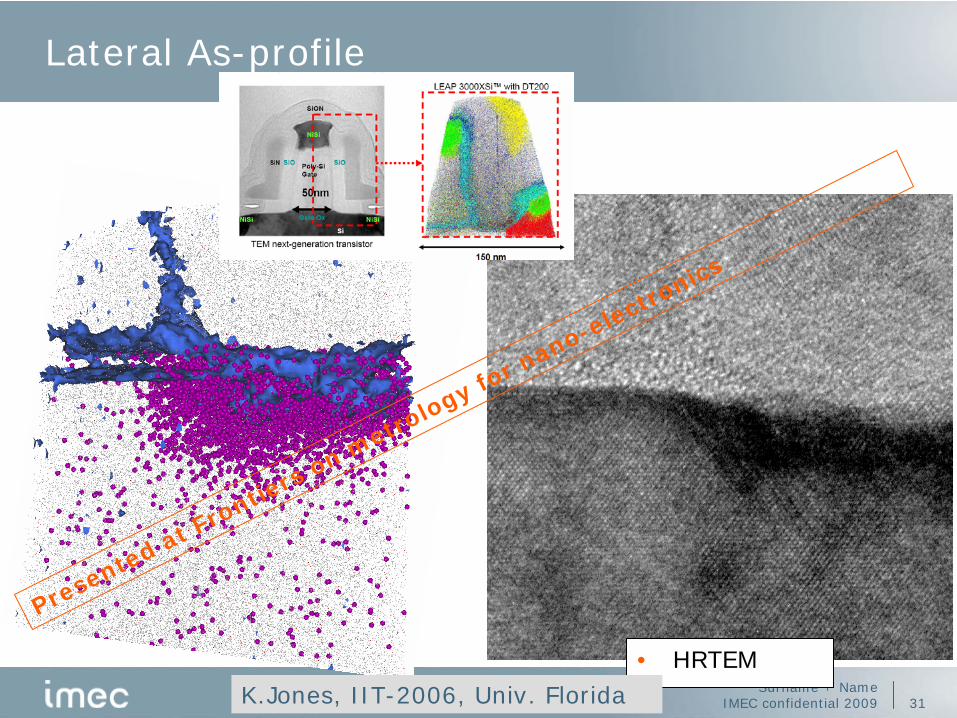
Lateral As-profile
• HRTEMK.Jones, IIT-2006, Univ. Florida
Presented at Frontie
rs on metro
logy for n
ano-electronics

Surname + NameIMEC confidential 2009 32
20 nm
20 nm
120 nm
3D-dopant profiling counting atoms
1 cts ~ 5 e19 at/cm3
Presented at Frontie
rs on metro
logy for n
ano-electronics

Surname + NameIMEC confidential 2009 33
FINFET underdiffusion : Counting single atoms with the atomprobe…
Gate
10 x 1 x1 = 500 Si atoms5e19 ~ 0.5 cts/pixel
Gate
Fin
1-2 nm
10 nm
60 nm
•Gradients : 1nm/dec
5e20 ~ 5 cts/pixel
5e19 ~ 0.5 cts/pixel
•Registration to gate (LER)Presented at F
rontiers on m
etrology fo
r nano-electro
nics

Surname + NameIMEC confidential 2009 34
Conclusions
• FINdoping fabrication and metrology is a major challenge– I/I ( ) , plasma doping ( ), VPD ()
• Metrology– conformality :
• SIMS through FINs• Resistors• S/D area’s : X-SSRM
– 3D-profiles
• Pseudo 3D-SSRM : dedicated test structures• 3D-Atomprobe : statistics!!!
Presented at Frontie
rs on metro
logy for n
ano-electronics
Surname + NameIMEC confidential 2009 35
Acknowledgements
Device fabricationHighly automated volume
nm-scale characterizationSkillfull experts
•The art of many student-experts :
M.Meuris, P.De Wolf, D.Alvarez, T.Hantschel, T.Trenkler, M.Fouchier, N.Duhayon, W.Polspoel, J.Mody, T.Janssens, S.Koelling,M.Gilbert, H.Bender, O.Richard,
•Collaboration Cameca (LAWATAP)

Surname + NameIMEC confidential 2009 36