ele - e202 electrical instruments 2 lab #1 safety lab page...
TRANSCRIPT
Electric Circuits ECE 2262 Department of Electrical and Computer Engineering
Page 1 of 13 V.4, Fall 2018
Lab 3 Transient Response of RC & RL Circuits
Last Name:
First Name:
Student Number:
Lab Section: Monday
Tuesday
Wednesday
Thursday
Friday
TA Signature:
Note: The Pre-Lab section must be completed prior to the lab session.
Lab objectives o Transient response of RC circuits
o Transient response of RL circuits
o Simulated inductor circuit using Op-Amps
Equipment o Oscilloscope
o Signal generator
o ADALM1000 (M1K)
o Resistor, capacitor, inductor, op-amp
Pre Lab Mark: /2
Lab Mark: /8
Total: /10

Electric Circuits ECE 2262 Department of Electrical and Computer Engineering
Page 2 of 13 V.4, Fall 2018
Pre Lab
RC Circuits
Assume that the switch S has been at the position shown in Figure 1 for a long time and it
toggles at time t=0. Answer the following questions.
1. As you will see in your upcoming course notes, Vo can be derived by writing a KVL after the
switch has toggled. The output, Vo, can be calculated in terms of V1 and V2 as a function of
time for t≥0 as follows:
𝑉2 = 𝑅. 𝑖𝑐(𝑡) + 𝑉𝑜(𝑡) => 𝑅𝐶𝑑𝑉𝑜(𝑡)
𝑑𝑡+ 𝑉𝑜(𝑡) = 𝑉2
This is a first-order linear ordinary differential equation (ODE), which has the following
solution:
𝑉𝑜(𝑡) = (𝑉1 − 𝑉2)𝑒−𝑡𝑅𝐶⁄ + 𝑉2
This equation is called the transient response of the capacitor voltage. How much is Vo at t=0+
(that is the moment right after the switch is toggled) and t=∞? Explain if these values are what
you expected.
2. An RC/RL circuit which has only one C or L and consists of DC sources and switches has a
general solution for the voltages and currents:
𝑥(𝑡) = 𝐴 + 𝐵𝑒−𝑡
τ⁄
τ is the time constant of the circuit which is equal to RC in this case as can be seen in the
comparison of the last two equations. How much is Vo at t=5τ? Normally t=5τ is the time
needed to allow the circuit reach its steady state.
Figure 1
Electric Circuits ECE 2262 Department of Electrical and Computer Engineering
Page 3 of 13 V.4, Fall 2018
3. How does it affect the circuit time constant if the internal resistor of the voltage source V2 was
nonzero (Rs≠0)?
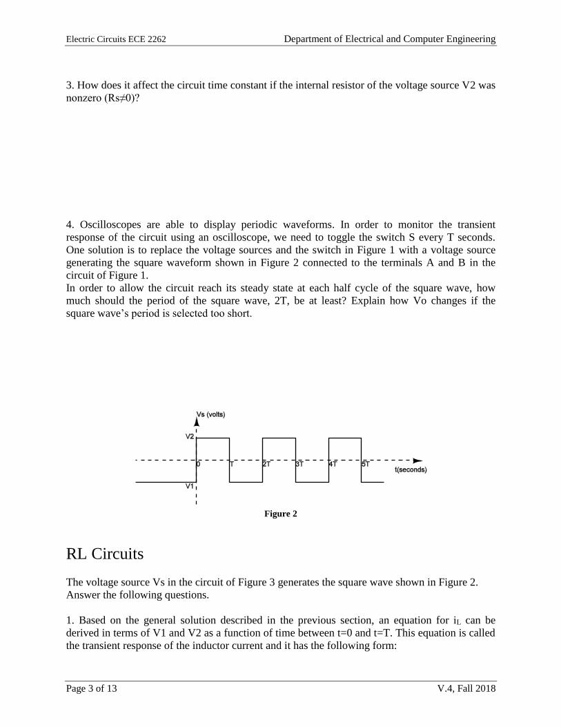
4. Oscilloscopes are able to display periodic waveforms. In order to monitor the transient
response of the circuit using an oscilloscope, we need to toggle the switch S every T seconds.
One solution is to replace the voltage sources and the switch in Figure 1 with a voltage source
generating the square waveform shown in Figure 2 connected to the terminals A and B in the
circuit of Figure 1.
In order to allow the circuit reach its steady state at each half cycle of the square wave, how
much should the period of the square wave, 2T, be at least? Explain how Vo changes if the
square wave’s period is selected too short.
Figure 2
RL Circuits
The voltage source Vs in the circuit of Figure 3 generates the square wave shown in Figure 2.
Answer the following questions.
1. Based on the general solution described in the previous section, an equation for iL can be
derived in terms of V1 and V2 as a function of time between t=0 and t=T. This equation is called
the transient response of the inductor current and it has the following form:

Electric Circuits ECE 2262 Department of Electrical and Computer Engineering
Page 4 of 13 V.4, Fall 2018
𝑖𝐿 =(𝑉1 − 𝑉2)
𝑅𝑒−(𝑅
𝐿⁄ ) 𝑡 +𝑉2
𝑅
How much is iL at t=0+ and t=∞? Explain whether the results are acceptable.
2. Assuming T=5τ, so the period is long enough such that the circuit reaches its steady state.
How much is the inductor current at t=T?
3. What is the time constant of the circuit? How does it affect the circuit time constant if the
internal resistor of the voltage source V2 was nonzero (Rs≠0)?
4. Oscilloscopes are basically voltmeters with the capability of displaying the measured voltages.
However, in the circuits including inductors usually inductors’ currents are of more interest to
monitor. In such cases, one may pick a voltage in the circuit which is proportional to the
inductor’s current to display on the oscilloscope. Is there any element in the circuit of Figure 3
whose voltage is proportional to the inductor current? Explain.
Figure 3

Electric Circuits ECE 2262 Department of Electrical and Computer Engineering
Page 5 of 13 V.4, Fall 2018
Simulated inductor
An inductor is usually constructed as a coil of conducting material, typically copper wire,
wrapped around a core either of air or of magnetic material.
Figure 4 shows some examples of coil inductors. Building an inductor has always been a
challenge in electrical engineering. Especially when a large value of inductance is needed, the
size and the weight of the inductors are undesired. Figure 5, for instance, shows a case that the
inductor is significantly larger than the rest of the circuit components.
Figure 4
Figure 5
In low voltage applications, it is very efficient to use a circuit that is equivalent to an inductor.
Figure 6.a shows a circuit consisting of two resistors, one capacitor, and one Op-Amp that is
equivalent to an inductor of L=R1×R2×C in series with the resistor R1. Selecting a small value
for R1, the equivalent circuit will be close to an ideal inductor. The limit of this model is that one
of the terminals of the inductor must be grounded.
Figure 6
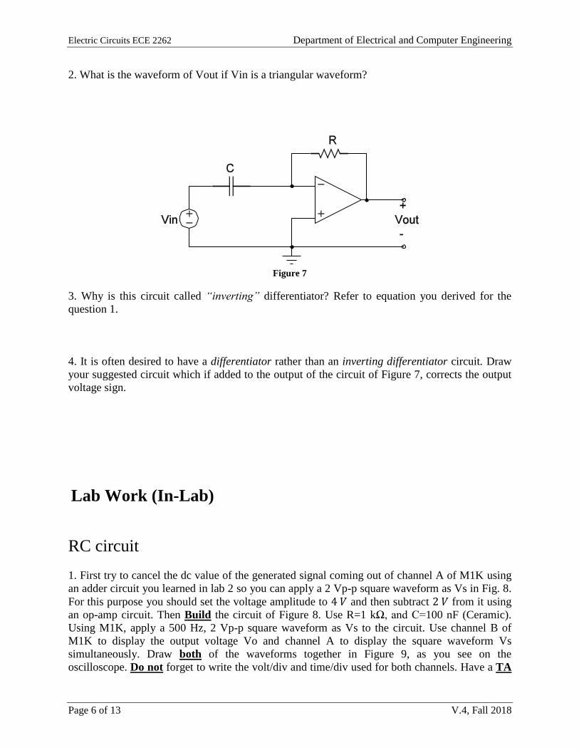
Inverting differentiator
Figure 7 shows a simple differentiator circuit. Answer the following questions.
1. Derive an equation for Vout in terms of Vin as a function of time.
Electric Circuits ECE 2262 Department of Electrical and Computer Engineering
Page 6 of 13 V.4, Fall 2018
2. What is the waveform of Vout if Vin is a triangular waveform?
Figure 7
3. Why is this circuit called “inverting” differentiator? Refer to equation you derived for the
question 1.
4. It is often desired to have a differentiator rather than an inverting differentiator circuit. Draw
your suggested circuit which if added to the output of the circuit of Figure 7, corrects the output
voltage sign.
Lab Work (In-Lab)
RC circuit
1. First try to cancel the dc value of the generated signal coming out of channel A of M1K using
an adder circuit you learned in lab 2 so you can apply a 2 Vp-p square waveform as Vs in Fig. 8.
For this purpose you should set the voltage amplitude to 4 𝑉 and then subtract 2 𝑉 from it using
an op-amp circuit. Then Build the circuit of Figure 8. Use R=1 kΩ, and C=100 nF (Ceramic).
Using M1K, apply a 500 Hz, 2 Vp-p square waveform as Vs to the circuit. Use channel B of
M1K to display the output voltage Vo and channel A to display the square waveform Vs
simultaneously. Draw both of the waveforms together in Figure 9, as you see on the
oscilloscope. Do not forget to write the volt/div and time/div used for both channels. Have a TA

Electric Circuits ECE 2262 Department of Electrical and Computer Engineering
Page 7 of 13 V.4, Fall 2018
sign in the box after showing the results. Write down the peak to peak voltage of Vo. Calculate
the time constant of the circuit.
Vo(p-p)= ……………….….Volts Time constant of the circuit =………………………=………….…………….Seconds
Figure 8
Figure 9
Channel 1 Channel 2 TA signature
Volt/Div (Volts)
Time/Div (Seconds)
Now change the frequency of the square waveform to 2 kHz and do not make any changes to its
amplitude. How much is the peak to peak voltage of Vo? Explain why it is not the same as the
previous case.
Vo(p-p)=………….Volts

Electric Circuits ECE 2262 Department of Electrical and Computer Engineering
Page 8 of 13 V.4, Fall 2018
Explain here:
………………………………………………………………………………………………………
………………………………………………………………………………………………………
………………………………………………………………………………………………………
………………………………………………………………………………………………………
Change the frequency of the square waveform to 10 kHz and draw both the square waveform
Vs and the output voltage Vo together in Figure 10. Ask a TA sign in the box. What type of
waveform does Vo look like?
Answer here: It looks like a ……................... waveform.
How much is the peak to peak voltage of Vo?
Vo(p-p)=………………Volts.
Check the one which appropriately represents the function of this circuit when f=10 kHz?
Differentiator Integrator
Figure 10
Channel 1 Channel 2 TA signature
Volt/Div (Volts)
Time/Div (Seconds)
Electric Circuits ECE 2262 Department of Electrical and Computer Engineering
Page 9 of 13 V.4, Fall 2018
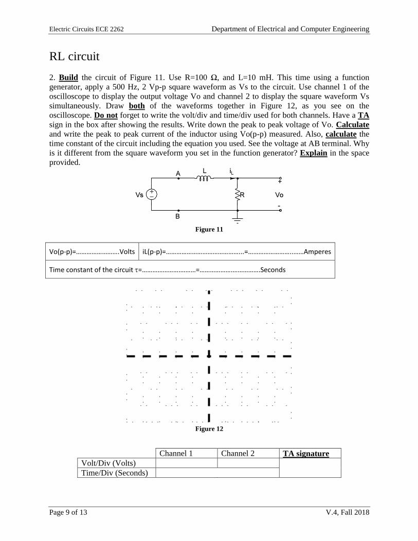
RL circuit
2. Build the circuit of Figure 11. Use R=100 Ω, and L=10 mH. This time using a function
generator, apply a 500 Hz, 2 Vp-p square waveform as Vs to the circuit. Use channel 1 of the
oscilloscope to display the output voltage Vo and channel 2 to display the square waveform Vs
simultaneously. Draw both of the waveforms together in Figure 12, as you see on the
oscilloscope. Do not forget to write the volt/div and time/div used for both channels. Have a TA
sign in the box after showing the results. Write down the peak to peak voltage of Vo. Calculate
and write the peak to peak current of the inductor using Vo(p-p) measured. Also, calculate the
time constant of the circuit including the equation you used. See the voltage at AB terminal. Why
is it different from the square waveform you set in the function generator? Explain in the space
provided.
Figure 11
Vo(p-p)=…………………….Volts iL(p-p)=……………………………………...=……………………..……Amperes
Time constant of the circuit =………………….………=……………….…………….Seconds
Figure 12
Channel 1 Channel 2 TA signature
Volt/Div (Volts)
Time/Div (Seconds)
Electric Circuits ECE 2262 Department of Electrical and Computer Engineering
Page 10 of 13 V.4, Fall 2018
Explain here:
………………………………………………………………………………………………………
………………………………………………………………………………………………………
………………………………………………………………………………………………………
Now, change the frequency of the square waveform to 3 kHz and do not make any change to its
amplitude. How much is the peak to peak voltage of Vo? Calculate and write the peak to peak
current of the inductor using Vo(p-p) measured.
Vo(p-p)=…………………….Volts iL(p-p)=……………………………………...=……………………..……Amperes
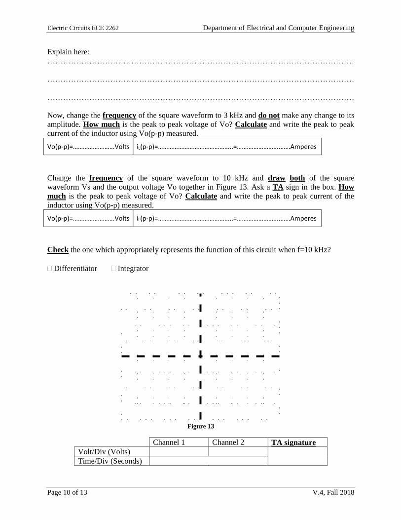
Change the frequency of the square waveform to 10 kHz and draw both of the square
waveform Vs and the output voltage Vo together in Figure 13. Ask a TA sign in the box. How
much is the peak to peak voltage of Vo? Calculate and write the peak to peak current of the
inductor using Vo(p-p) measured.
Vo(p-p)=…………………….Volts iL(p-p)=……………………………………...=……………………..……Amperes
Check the one which appropriately represents the function of this circuit when f=10 kHz?
Differentiator Integrator
Figure 13
Channel 1 Channel 2 TA signature
Volt/Div (Volts)
Time/Div (Seconds)
Electric Circuits ECE 2262 Department of Electrical and Computer Engineering
Page 11 of 13 V.4, Fall 2018
Simulated inductor
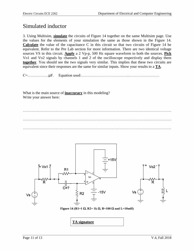
3. Using Multisim, simulate the circuits of Figure 14 together on the same Multisim page. Use
the values for the elements of your simulation the same as those shown in the Figure 14.
Calculate the value of the capacitance C in this circuit so that two circuits of Figure 14 be
equivalent. Refer to the Pre Lab section for more information. There are two identical voltage
sources VS in this circuit. Apply a 2 Vp-p, 500 Hz square waveform to both the sources. Pick
Vo1 and Vo2 signals by channels 1 and 2 of the oscilloscope respectively and display them
together. You should see the two signals very similar. This implies that these two circuits are
equivalent since their responses are the same for similar inputs. Show your results to a TA.
C=……………..μF. Equation used:………………………………..……………………
What is the main source of inaccuracy in this modeling?
Write your answer here:
………………………………………………………………………………………………………
………………………………………………………………………………………………………
………………………………………………………………………………………………………
Figure 14 (R1=1 Ω, R2= 1k Ω, R=100 Ω and L=10mH)
TA signature
Electric Circuits ECE 2262 Department of Electrical and Computer Engineering
Page 12 of 13 V.4, Fall 2018
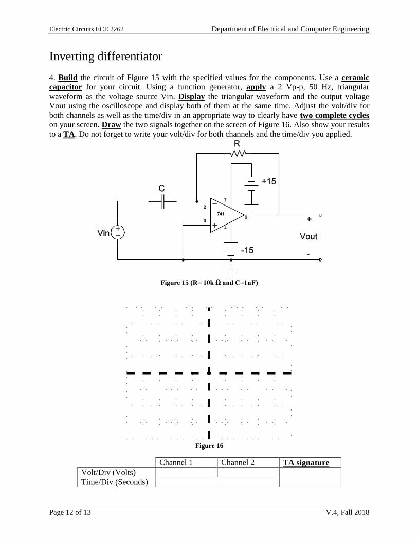
Inverting differentiator
4. Build the circuit of Figure 15 with the specified values for the components. Use a ceramic
capacitor for your circuit. Using a function generator, apply a 2 Vp-p, 50 Hz, triangular
waveform as the voltage source Vin. Display the triangular waveform and the output voltage
Vout using the oscilloscope and display both of them at the same time. Adjust the volt/div for
both channels as well as the time/div in an appropriate way to clearly have two complete cycles
on your screen. Draw the two signals together on the screen of Figure 16. Also show your results
to a TA. Do not forget to write your volt/div for both channels and the time/div you applied.
Figure 15 (R= 10k Ω and C=1µF)
Figure 16
Channel 1 Channel 2 TA signature
Volt/Div (Volts)
Time/Div (Seconds)
Electric Circuits ECE 2262 Department of Electrical and Computer Engineering
Page 13 of 13 V.4, Fall 2018
How much is the peak to peak voltage of Vout?
Vout(p-p)=…………Volts.
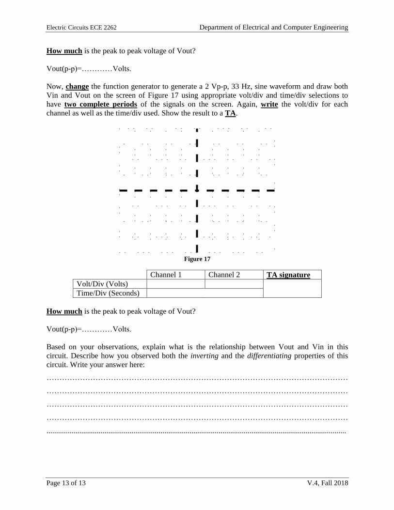
Now, change the function generator to generate a 2 Vp-p, 33 Hz, sine waveform and draw both
Vin and Vout on the screen of Figure 17 using appropriate volt/div and time/div selections to
have two complete periods of the signals on the screen. Again, write the volt/div for each
channel as well as the time/div used. Show the result to a TA.
Figure 17
Channel 1 Channel 2 TA signature
Volt/Div (Volts)
Time/Div (Seconds)
How much is the peak to peak voltage of Vout?
Vout(p-p)=…………Volts.
Based on your observations, explain what is the relationship between Vout and Vin in this
circuit. Describe how you observed both the inverting and the differentiating properties of this
circuit. Write your answer here:
………………………………………………………………………………………………………
………………………………………………………………………………………………………
………………………………………………………………………………………………………
………………………………………………………………………………………………………
...........................................................................................................................................................