能源科技與環境概論 太陽能電池導論mx.nthu.edu.tw/~hytuan/courses-files/2015...
TRANSCRIPT

能源科技與環境概論
太陽能電池導論
Hsing-Yu Tuan (段興宇)
Department of Chemical Engineering, National Tsing-Hua University

Various types of solar cells
solar cells
silicon
compound
organic
crystalline
thin film amorphous
single crystalline
polycrystalline
III-V(GaAs)
poly crystalline thin film
dye sensitized
polymer
single crystalline
CIGS
CdTe

Pick right materials as absorption layer
- Good absorption coefficient to harvest light - Suitable band gap

E
CB
k–k
Direct Bandgap
(a) GaAs
E
CB
VB
Indirect Bandgap, Eg
k–k
kcb
(b) Si
E
k–k
Phonon
(c) Si with a recombination center
Eg
Ec
Ev
Ec
Ev
kvb VB
CB
ErEc
Ev
Photon
VB
(a) In GaAs the minimum of the CB is directly above the maximum of the VB. GaAs istherefore a direct bandgap semiconductor. (b) In Si, the minimum of the CB is displaced fromthe maximum of the VB and Si is an indirect bandgap semiconductor. (c) Recombination ofan electron and a hole in Si involves a recombination center .
?1999 S.O. Kasap, Optoelectronics (Prentice Hall)
Direct band gap and indirect band gap structure
-We prefer direct semiconductor materials since they can absorb light more efficiently

Absorption of semiconductors
-Si and Ge’s absorption coefficient increase slowly with increased energy

real ηmax is only around 30% due to loss of other facters
ηmax(%) vs Eg (eV) under AM1.5
Eg: 1.0 – 1.5 eV is the best range

Electron energy, E
Conduction Band (CB)Empty of electrons at 0 K.
Valence Band (VB)Full of electrons at 0 K.
Ec
Ev
0
Ec+χ
(b)
Band gap = Eg
(a)
Covalent bond Si ion core (+4e)
(a) A simplified two dimensional view of a region of the Si crystalshowing covalent bonds. (b) The energy band diagram of electrons in theSi crystal at absolute zero of temperature.?1999 S.O. Kasap, Optoelectronics (Prentice Hall)
Semiconductor band, using Si as an example

Doping of Si: increase the conductivity of intrinsic Si
Donors: P, As, Sb (Column V elements ) , n-type, provide one additional electron Acceptors: B, Ga, In, (Column III elements), p-type provide one additional hole
P+ B- -
-weakly bound -bonding strength EB~ 0.05 eV (Si bonding ~1.12 eV)
Donors EB Acceptors EB
Sb 0.039 eV B 0.045 eV P 0.044 eV Al 0.057 eV As 0.049 eV Ga 0.065 eV In 0.16 eV
Ec
Ev
ED 0.044 eV (P)
0.057 eV (Al) EA
Majority carrier - electron in a n-type material hole in a p-type material Minority carrier – hole in a n-type material electron in a p-type material
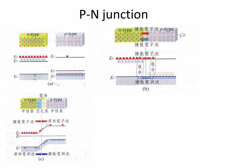
P-N junction
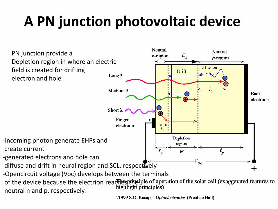
A PN junction photovoltaic device
-incoming photon generate EHPs and create current -generated electrons and hole can diffuse and drift in neural region and SCL, respectively -Opencircuit voltage (Voc) develops between the terminals of the device because the electrion reaches the neutral n and p, respectively.
PN junction provide a Depletion region in where an electric field is created for drifting electron and hole

Device structure of a Si solar cell
Finger electrodes
p
n
Bus electrode for current collection
- finger electrodes were made to allow light pass through the device - a thin antireflection coating on the surface reduces light reflection and allow more lighte to enter the device -surface texturization to for multiple light reflection and increase light path
0.2 μm
200 μm
In order to capture more light
surface texturization Incident light
(1)
(2)
(3)

Schematic of a semocnoductor solar cell

Video

IV curve of a solar cell
Voc (open circuit voltage) -when output current approaches zero, the voltage develops between two terminals ideally Voc~Eg at 0K and inverse proportional to temperature Jsc (short-circuit current) -like the device connect the device with metal circuit, close to photogenerated current
ocsc
mpmpmpmpmp VJ
VJFFVJP
×
×=×= ;
%100/
%100
%100
%100)(
( )
×××=
××
××
×=
××
=
×=
inscoc
scoc
mpmp
in
scoc
in
mpmp
in
mp
PFFJV
JVJV
PJV
PJV
PpowersolarIncident
PpoweroutputPVMaximumη
FF (fill factor): We want FF close to 1

Solar cell efficiency :an example
0
1
2
3
4
5
6
7
8
9
10
0 0.2 0.4 0.6 0.8 1
J(mA/cm2)
V(V)
η=PMP /Pin x100%=FF*VocJsc/ Pin x100% (輸出電功率/入射光功率) P in =100 mW/cm2
PMP=VMP*JMP=0.55*5.9716=3.28mW/cm2 η =3.28/100*100%=3.28% Voc=0.72 V Jsc=7.1464 mA/cm2 FF=VMP*JMP/Voc*Jsc =3.28/(0.72*7.14)=0.63
(0.55,5.9716)
VMP
JMP
Voc
Jsc
Voc: 開路電壓 (open circuit voltage), 當輸出電流趨近於零,相 對太陽電池兩電極端點沒有連接所得到的電壓 Jsc:短路電流(short circuit current) 如將照光的pn二極體兩端的金屬電極用金屬線連接, 造成短路, 此短路電流等於光電流
η and FF in this device ?

100% Incident radiation
× 0.74 Insufficient photon energyhυ < Eg
× 0.59
Excessive photon energyNear surface EHP recombinationhυ > Eg
× 0.95 Collection efficiency of photons
× 0.6 Voc ≈ (0.6Eg)/(ekB)
× 0.85
η ≈ 21%
FF ≈ 0.85
Overall efficiency
Accounting for various losses of energy in a high efficiency Sisolar cell. Adapted from C. Hu and R. M. White, Solar Cells(McGraw-Hill Inc, New York, 1983, Figure 3.17, p. 61).?1999 S.O. Kasap, Optoelectronics (Prentice Hall)
Various losses of solar energy of a Si solar cell during processing
Silicon band gap is 1.1 eV, and the device loses all photon energy less than 1.1 eV
Voc is inverse proportional to temperature, so not equals to Eg
Only 43.6% remaining! Excessive photon energy Near surface EHP recombination
Antireflection coating is not perfect
The highest efficient of a real photovoltaic device that uses a single crystal of Si Is about 24.7% (澳洲新南威爾斯 大學)
device fabrication resistance

Single/poly crystalline Si solar cell fabrication process
etch in a strong acidic or alkaline solution
etch in a weak acidic or alkaline solution
liquid glass containing P is distributed on one side of the wafer by spraying or spinningand heated
(the wafer are placed in a belt furnace And heated about 900 °C
The reflectivity is still round 30%,H:SiNx is deposited on the cell to reduce more the reflectivity
metal contacts are made by screen printing
Metallic contacts are heated and Etch trough the antiflecton coating
P-type ingot was cut
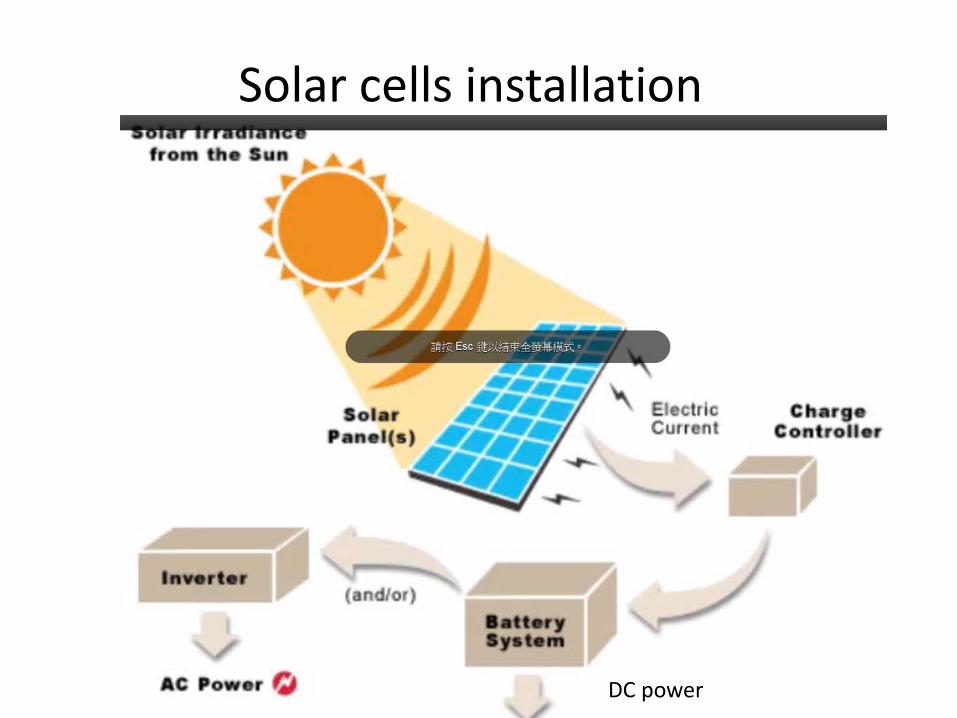
Solar cells installation
DC power

Next step of crystalline Si solar cell

貳、發展現況(續) 五、我國太陽光電產業鏈
Installation:茂迪、台達電、廣運、友達、聯相、宇通、富陽、永盛能源、有成、綠能、大金、東城、冠宇宙、太陽動力、鼎鼎、聚恒、金華成、中國大陸電器、羅森、全面性、伸浦、崇越、統昱、永旭、台邦、傳典、高鋒、華旭環能、工易、耀能、上揚、錸德、光寶綠能、詠通、華城、亞力、駿成、曜晟、寶球、明宜、元太、伸浦、新世紀、金頓、海灣、泰新、安慶、昇暉、雄雞 System Parts:台玻、元璋、太美、城東、力鋼、元一、高鋒、法隆、泉鋼、盈正豫順、明碁材料、達方、台虹、碩禾、致嘉、台塑、暘益、台聚、新輝、昇貿、宏致、泰和、建和興、科宥 Equipment:均豪、廣運、欽揚、東遠、志聖、帆宣、北儒、翔勝、致茂、綠色 Product:亞通、東城、強而青、鯨威、日光能、茂迪、中國大陸電器、同昱、旭辰、旭邦、科宥、信合、千附、永炬、日曜、宇能、智柏、登陽 、誼成、森富國際、
>100 Companies
Poly- Silicon
Ingots/ Wafer
Solar Cell
PV Module
PV System & Installation
Solar Grade Silicon
Si Ingot & Wafers
Wafer-based Solar Cell -Mono-Si, Multi-Si, GaAs Thin-film Solar Cell -a-Si/µ-Si, CIS, -Dye Sensitized Solar Cell CPV Solar Cell
PV Modules
Installation System Parts -Inverter, BOS… Equipment Product
Up Stream Mid Stream Down Stream
Indu
stry
C
ompa
ny
•中美晶 •綠能 •合晶 •統懋 •峰毅 •茂迪 •旭晶能源 •晶耀 •達能 •國碩 •昱成光能 •友達晶材 12 Companies
福聚太陽能 友達晶材 寶德能源 實聯能源 科冠 山陽科技 6 Companies
•矽晶電池:茂迪、益通、旺能、昱晶、新日光、昇陽、茂矽、太陽光電、太極、燿華、長生能源、旭泓、亞崙、尚陽、強茂、樂福、聯景、元晶、英穩達、友達 •矽薄膜電池:綠能、聯相、富陽、宇通、八陽、旭能 •CIGS電池:綠陽、新能、太陽海、正峰新、亞化、威奈聯合、台積電 •聚光型電池:全新、華上、禧通、台達電、晶電、宏捷、華旭、億芳、瀚昱、海德威、太聚、綠源、吉泰、亞飛、禾晶 •DSSC:健鼎、福盈、永光、镸興、台塑
> 54Companies
• 頂晶 • 知光 • 英懋達 • 生耀 • 科風 • 茂暘 • 錸德 • 有晴 • 大晶 • 全能 • 安集 • 茂鑫 • 強茂 • 有成 • 友達 • 綠晁 • 鼎笙 17Companies
歷年廠家數: 2005=40 2006=50 2007=76 2008=100 2009=123 2010>160

15.1% 6.7% 28.2% 36.4% 6.9% 6.7%
28.1% 10.8% 27.4% 21.8% 6.4% 5.5%
32.7% 11.6% 25.1% 16.0% 5.5% 9.1%
37.5% 12.3% 19.8% 12.6% 4.4% 13.4%
46.4% 14.1% 13.2% 7.8% 4.7% 13.8%
56.6% 11.4% 8.7% 6.0%3.1% 14.2%
0% 10% 20% 30% 40% 50% 60% 70% 80% 90% 100%
2006
2007
2008
2009
2010
2011 中國大陸
台灣
歐洲
日本
美國
其他
歐洲與日本之電池產量由2006年市占率約30%下降至2011年的10%以下。 太陽光電生產基地持續向亞洲移動趨勢不變,中國大陸與臺灣生產比例近全球
70%。 大陸挾其成本優勢與政策支持,成為全球最大製造國,2011年產值達2536億元人
民幣。

Thin film solar cell: use Si as an example
- required thickness of thin film solar cell is around 0.5 μm, 1/500 of that of wafer based solar cell - material cost is very low

Advantages of thin film solar cells
1. low raw materials are required for fabrication
2. light transmission is better
3. more competitive price (CdTe, US$1 per watt ; First Solar, stock price is US$180 )
4. frameless design
5. Ideal for BIPV( building integrated photovoltaic)


Device structure of amorphous Si solar cell
-a-Si’s absorption coefficient at visible light is one order of magnitude than c-Si , so only 10-30 nm is needed to capture most photon in the visible region -thickness of p and n type are around 10-30nm, thickness of i layer is less than 500 nm

Structure of an amorphous Si solar cell
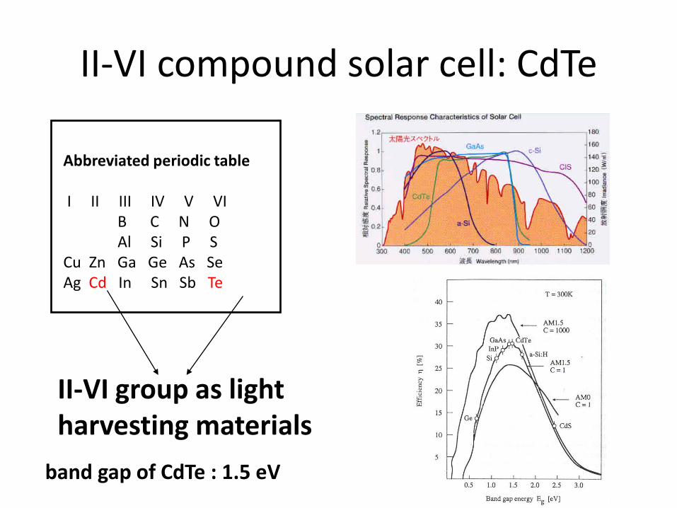
II-VI compound solar cell: CdTe
Abbreviated periodic table I II III IV V VI B C N O Al Si P S Cu Zn Ga Ge As Se Ag Cd In Sn Sb Te
II-VI group as light harvesting materials
band gap of CdTe : 1.5 eV

Device structure of a CdTe solar cell
P-type: CdTe n-type: CdS

First solar
Pallas 綜合外電報導 / SolarExchange 美國太陽能廠商First Solar於去年第四季生產成本降到每瓦0.98美元 美國太陽能模組製造商First Solar(Nasdaq: FSLR)於24日宣布, 2008年第四季平均生產成本降到每瓦0.98美元,成為首家低於每瓦1美元的太陽能廠商。 美國太陽能模組製造商First Solar(Nasdaq: FSLR)於24日宣布,2008年第四季平均 生產成本降到每瓦0.98美元,成為首家低於每瓦1美元的太陽能廠商。 First Solar於2004年開始商業化生產以來,2008年產能成長約2500 % 達到500 MW。 2009年產能將再增加一倍,達到1GW。這相當於一般核電廠的規模。 這些成長率隨著成本迅速降低而提高。生產成本自2004年以來降了超過三分之二, 從每瓦3美元降到每瓦1美元不到。First Solar有信心能基於First Solar未用盡的技術 和製程的潛力,進一步再將成本降至更低。
Current production Cost of crystalline Solar cell is around US 2/Wp

Band gap and optical absorption of CIGS
Muller, semiconductor for solar cells, 1993
CISe2:1.0 eV CIGS:1.0-1.6 eV CIS:1.3-1.5 eV
-CIGS’s band gap is in the range of 1.1 to 1.5 ev
Efficiency = FFVocIsc Pin

I-III-V2 compound solar cell: (CIGS)
Cu(InGa)Se2 (2µm)
Soda lime glass Mo (0.5 µm)
n-typeCdS (0.05 µm)
HR-ZnO/n+-ZnO (0.5µm)
Current collection grid
total device thickness less than 5 µm (Crystalline Si module~200 µm)
Schematic picture

Compared to CdTe solar cells
Cu(InGa)Se2 (2µm)
Soda lime glass Mo (0.5 µm)
n-typeCdS (0.05 µm)
HR-ZnO/n+-ZnO (0.5µm)
Current collection grid
Schematic picture
Much less Cd required

An example of vaccum-based CIGS film deposition
Y. Hamakawa Thin-film solar cells,

Vaccum-based CIGS film deposition
-Highest efficiency (lab scale: 18~20%) -Usually UHV/MBE -Cost prohibitive (but <cryst-Si)
General drawbacks: -Difficult to achieve controlled-stoichiometry over large device areas -Manufacturing equipment is “very” expensive (> NT 0.1 billion) -The deposition process is time-consuming -Poor materials utilization (30-50%) -Low throughput

36
Non-Vacuum Processing
-Synthesize colloidal nanocrystals with controlled CIGS stoichiometry and deposit layer -Roll-to-roll manufractruing process

37
Nano solar- Nanoparticle as ink for printable solar cell
CIGS particle ink
has denmostrated a 1GW coater in a movie
Flexible solar cell
Roll-to-roll processing
Add a video

Silicon Wafer cells
Vacuum-based thin film
Roll-printed thin film
Process Si wafer processing
High vacuum depositon
Roll-to-roll printing
Process Yield
Robust Fragile Robust
Materials Utilization
30% 30-60% Over 97%
Throughput 1 2-5 10-25


Nanosolar, Thin-Film Solar Hype Firm, Officially Dead U.S. CIGS solar assets are being auctioned off after more than $400 million in VC investment. by Eric Wesoff July 12, 2013

CIGS Rocks! 2010/July
【時報記者沈培華台北報導】台積電 (2330) 新事業總經理蔡力行表示, 台積電將以CIGS薄膜產品進軍太陽能產業,以五年期間朝全球前五大廠邁進, 產能規模將達1GW規模,並看好此事業對台積電是有獲利與高成長潛力的新事業。 台積電今天舉行先進薄膜太陽能技術研發中心暨先期量產廠房動土典禮。 新事業總經理蔡力行表示,全球太陽能電池市場將持續成長,預期2009年至 2015年全球太陽能電池市場年複合成長率可望達23%;其中,銅銦鎵硒(CIGS) 因具有薄膜的低成本價格等優勢,成長率將最高,年複合成長率將達115%。 台積電因此將以CIGS薄膜產品為主力,進軍太陽能產業。 台積電先進薄膜太陽能廠第一期將投資約79.2億,預計2012年量產200百萬瓦(MW) ,終期產能為700百萬瓦(MW)。台積電董事長張忠謀並預估,2015年太陽能佔 台積電營收比重可望達10%。蔡力行表示,台積電三年內CIGS薄膜太陽能電池 模組轉換效率將達14%,產能規模將約300至500百萬瓦,預期3至5年轉換效率 將進一步提升至16%,產能規模將達1GW規模。

薄膜太陽能翻身 台積電產能衝3倍 全球龍頭廠轉盈 產業前景漸撥雲見日 2014/Feb
台積電旗下銅銦鎵硒(CIGS)薄膜太陽能廠目前年產能為40百萬瓦(MWp),隨著整體市況轉佳、訂單滿載且技術獲得重大突破,台積電第4季CIGS年產能將擴增到120MWp,達到3倍規模,太陽能業者透露,以台積電在太陽能領域穩紮穩打風格來看,這次產能出現大躍進,凸顯CIGS接單情況明顯轉佳,業界紛預期台積電太陽能事業可望邁向獲利。不過,台積電發言體系表示,目前針對財務部分不予置評。 全球最具代表性的CIGS薄膜太陽能龍頭大廠是日本昭和殼牌石油旗下子公司Solar Frontier,年產能規模達900MWp,近年來一直陷入虧損困境翻不了身,然近期財報終於首度轉虧為盈,2013年旗下產能全數滿載,年營收暴增8成,並計劃在日本東北(Tohoku)擴增150MWp產能的CIGS新廠,預計2015年投產。

台積太陽能步上關廠 業界:成本難敵矽晶 2015/08/25 16:36
(中央社記者張建中新竹25日電)台積電100%持股子公司台積太陽能將於8月底結束工廠營運。業界人士認為,薄膜太陽能電池成本難敵矽晶太陽能電池,是迫使台積太陽能走向關廠的主因。 台積電新事業發展接連遭逢重大挫敗,旗下台積固態照明因較晚進入發光二極體(LED)產業,業界專利障礙與通路開發不易,考量短期難以轉盈,台積電今年初決定將台積固態照明全部股份賣予晶電。 台積電今天又宣布,旗下台積太陽能因是市場後進者,缺乏經濟規模,雖然轉換效率具領先優勢,但在成本上不具競爭力,即便執行最精進的成本減抑計畫,也將難以逆轉成本劣勢,將於8月底結束工廠營運。 台積電是於2009年成立新事業部,並陸續成立台積固態照明與台積太陽能,分別投入LED與太陽能產業,由前總執行長蔡力行領軍。隨著蔡力行轉往中華電信擔任董事長,台積固態照明與台積太陽能董事長由左大川接任。 台積太陽能成立之初,蔡力行曾表示,台積太陽能將以技術領先為主要策略。

Comparison of three thin film solar cells
Semiconductor Taiwan 2008

Tandom Junction Solar cells

Market distribution in 2009