variability aware svm macromodel based design centering of analog circuits
TRANSCRIPT
Analog Integrated Circuits and Signal Processing manuscript No.(will be inserted by the editor)
Variability Aware SVMMacromodel based Design Centering of Analog Circuits
the date of receipt and acceptance should be inserted later
Abstract Design centering is the term used for a procedure of obataining enhanced parametric yield of a circuit despite
variations in device and design parameters. The process variability in nanometer regimes manifest into these device and
design paramters. During design space exploration of analog circuits, a methodology to find design-instances with better
yield is necessitated; this would ensure that the circuit will function as per specifications after fabrication even with
impact of statistical variations. We need to evaluate circuit performance for a given instance of a circuit-design identified
by possessing a set of nomial values of device-design parameters. A lot of instantces need be searhed having different
sizes for a given circuit topology. HSPICE is very compute intensive. Instead, we employ macromodeling approach
for analog circuits based on support vector machine (SVM), which enables efficient evaluation of performance of such
circuits of different sizings during yield optimization loops. These performance macromodels are found to be as accurate
as SPICE and at the same time time-efficicient for use in sizing of analog circuits with optimal yield. Process variability
aware SVM macromodels are first trained and then used inside the Genetic algorithm loops for design centering of
different circuits, subsequently resulting into sized-circuit instances having optimal yield. Post design centering, the
sized circuits will be able to provide functions as per specifications upon fabrication. The application this design centering
approach as process variability analysis tool is illustrated on various circuits e.g. two stage op amp, voltage controlled
oscillator and mixer circuit with layouts drawn into 90 nmAMC technology. Keywords: Design centering, Macromodels,
Support Vector Machine, Yield, genetic algorithm, analog circuit sizing.
Address(es) of author(s) should be given
ManuscriptClick here to download Manuscript: springer-2011-final-nobib1.tex
1 2 3 4 5 6 7 8 9 1011121314151617181920212223242526272829303132333435363738394041424344454647484950515253545556575859606162636465
2
1 Introduction
The rapid scaling of CMOS technology has increased the significance and complexity of process variation. Process vari-
ation is the deviation of parameters from desired values due to limited controllability of a process. As MOS device size
continues to rapidly scale down into the ultra deep sub-micron regime, reliability of manufacturing tools decreases while
controlling design parameters. Random dopant fluctuation, annealing effects and lithographic limitation are some of the
factors contributing towards process variation. These process variations manifest into variation of device parameters such
as Threshold voltage, Oxide thickness, and Length of a transistor [22]. Variations in device parameters in turn affect per-
formance metrics of analog circuits leading to loss in post design parametric yield. Yield is usually predicted by carrying
out Monte Carlo analysis with circuit simulations for various process parameters. Process parameters are randomly and
simultaneously varied according to their respective probability density function. Circuit performances are then evaluated
for these multiple instances of process parameters. Because most circuits require very significant simulation time, the cost
of performing a Monte Carlo analysis can be prohibitive except for small components. Analytical Modeling approaches
[11] have been employed to model circuit performance as a function of process parameters. However, they compro-
mise on accuracy. Machine learning approaches have been reported for macromodeling of analog circuits [10,5]. These
are performance macromodels, which can be trained using data generated directly from SPICE. They are build around
suitable kernel functions as regression functions and are able to provide SPICE level accuracy. These SVM models can
then be efficiently used inside Monte Carlo analysis loop to predict parametric yield. Process variability analysis tool so
developed is used with Genetic Algorithm (GA) for Design centering of the performance parameters of the two stage
op-amp, voltage controlled oscillator (VCO) and mixer circuit. GA is chosen for its empirical robustness in nonlinear
and non convex objective functions.
The rest of the paper is organized as follows. In next section, we review the the work done in past regardign yield
ananlysis and optimization fo analog circuits. We discuss problem of design centering in Section 3. Theory of SVM
regression model and yield analysis is presented in Section 4. Proposed work and experimental setup are presented in
Section 5. Results are presented and discussed in Section 6, while we conclude in Section 7.
2 Related Work
An approach for yield optimzation is presented in [17]. It is based on specification-wise linearization of the perfor-
mances at the worst case points in the space of statistical parameters and linearization of the feasibility region. A robust
coordinate search is reported, which performs better than gradient based algorithm resulting in improvement in nom-
1 2 3 4 5 6 7 8 9 1011121314151617181920212223242526272829303132333435363738394041424344454647484950515253545556575859606162636465

3
inal point and reduction in variance of circuit performance simultaneously. Linearization before search ensures that
Monte-Carlo simulations are substantially reduced for later computations. Novelty of above approach is focus on design
relevant regions in all parameter space, which leads to improvement in quality of yield estimation and hence enables a
roboust technique for direct yield optimization. However, with increasing larger variations in nano-scale technologies
linearization of performance can yield inaccurate results as analog performance are strongly nonlinear in the presence of
large scale variations. The other drawback is the difficulty to know in advance the worst-case corner points. Further, the
coordinate search technique face the problem of finding the optimal search direction which is quite difficult.
The technique for design centering and yield enhancement of SiGe hetrojunction bipolar transistor is presented in
[15]. The proposed method uses neural network for device and circuit modeling. Neural network model developed from
experimental/simulation data are used for mapping input and output parameters of the device. The type of neural net used
for modeling in this paper is the multilayer perceptron (MLP) network consisting of three or more layers. The network
is trained using the error back-propagation algorithm with a sigmoidal activation function. These models are then used
in place of circuit simulators in Monte Carlo analysis to predict the yield in efficient way. Once the yield is determined,
yield optimization is performed using genetic algorithm. The neural network model does not require any assumptions
about the system behavior, so it can be used to develop complex models. However, the drawback with neural network
model is that these are black box models and do not offer any qualitative insight. Neural networks also suffer from
the existence of multiple local minima solutions as algorithm used to determine the weights is gradient descent search
algorithm which may be trapped in a local minimum. Another limitation with Neural networks is over learning i.e. the
neural model matches the training data very well but does not match unseen data, so model is not able to generalize.
An efficient response surface based parametric yield extraction algorithm for multiple correlated non-Normal ana-
log/RF performance distributions that are observed in sub-90 nm technology nodes has been proposed in [12]. The
proposed algorithm conceptually maps multiple performance constraints to a single auxiliary constraint. The auxiliary
constraint is analytically approximated as a quadratic function of process parameters to capture the nonlinearities in-
herent in most analog/RF performance variations. The efficacy of the proposed algorithm is demonstrated on low noise
amplifier and operational amplifier. In both cases quadratic approximation achieves much better accuracy and reduces
maximal error to 5%. Though yield extraction process is faster as compared toMonte Carlo analysis but suffer on account
of generality and accuracy.
Methodology for generating yield-aware pareto surface is presented in [18]. Pareto surface represent the best per-
formance that can be obtained from a given circuit topology across its complete design space. Points on yield-aware
1 2 3 4 5 6 7 8 9 1011121314151617181920212223242526272829303132333435363738394041424344454647484950515253545556575859606162636465
4
pareto surface ensures a fixed yield number, hence making it useful for hierarchical synthesis applications. A new, nom-
inal pareto generation algorithm is proposed, which uses efficient local latin-hypercube sampling resulting in fast Monte
Carlo analysis for generation of yield-aware pareto fronts. Methodology is demonstrated on computing yield-aware
pareto fronts for power and phase noise for a voltage controlled oscillator circuit (VCO). These yield-aware pareto fronts
helps to select an optimal VCO circuit for a phase locked loop.
3 Design Centering Problem
The objective of the design centering or yield maximization problem is to maximize the number of fabricated circuits
whose performance meets a set of desired specifications. The parametric yield of a circuit as defined by authors in [15]
is portion of the manufactured circuits that satisfies a set of acceptability constraints on performance defined by the
user. The parametric yield Y of a circuit can be expressed as in (1). Here, y is a vector of circuit performance features
of interest (e.g., open loop gain, phase margin, etc), fy(.) is the joint probability density function of y, and aY is the
output acceptability region in the y space defined by acceptability constraints yLi ≤ yi ≤ yUi , i.e., aY = {yi | yLi ≤ yUi }. We
maximize the yield Y over D, a feasible region of input parameters, x ∈D. To save computational time inherent in SPICE
we utilize macromodeling approach for analog circuits based on support vector machine, which provides efficient as well
as accurate mapping between input design parameters and output performance features of such circuits.
Y =
ˆ
aY
fy(y)dy (1)
4 SVM based Yield Analysis
SVM regression have emerged as an efficient technique for modeling complex nonlinear relationships [5]. In the proposed
design centering methodology, support vector models developed from SPICE simulation data are used for mapping input
and output parameters of the circuit. We use extended SVM macromodel [3] which utilizes efficient kernels, instead of
using conventional kernels. These models are then used to estimate yield, rather than performing a large number of time
consuming evaluations by circuit simulators.
4.1 SVMMacromodel
Our work is based on the theory from [23]. Suppose we are given a training data {(x1,y1), ...(xk,yk)} ⊂ RN ×R, where
RN represents input space. By a certain nonlinear mapping φ, the training pattern xt is mapped into some feature space,
1 2 3 4 5 6 7 8 9 1011121314151617181920212223242526272829303132333435363738394041424344454647484950515253545556575859606162636465
5
in which a real valued function y(x) is defined as in (2). Here, φ(.) : Rn → Rnh is the mapping to the high dimensional
and potentially infinite dimensional feature space. Given a training set {xk,yk}Nk=1, optimization problem as in (3) is
formulated in the primal weight space.
y(x) = ωTφ(x)+b with ω ∈ RN , b ∈ R (2)
P : minw,b,e
Jp(w,e) =12wTw+ γ
12
N
∑k=1e2k (3)
This formulation involves the trade off between a cost function term and a sum of squared errors governed by the
trade-off parameter γ. In the regression formalism the term 12w
Tw is no longer related to hyper-plane separation, but
instead determines the smoothness of the resulting model. In fact, the primal problem in the LS-SVM formalism is
wholly equivalent to a ridge regression problem formulated in the feature space, with parameter γ performing the role of
smoothing parameter. Proceeding to the dual Lagrangian-based formulation
D : maxα
L(w,b,e;α) (4)
L = Jp(w,e)−N
∑k=1
αk{wTφ(xk)+b+ ek− yk} (5)
where αk are Lagrange multipliers. The conditions for optimality are given by
⎧⎪⎪⎪⎪⎪⎪⎪⎪⎪⎪⎪⎪⎪⎨⎪⎪⎪⎪⎪⎪⎪⎪⎪⎪⎪⎪⎪⎩
∂L∂w = 0 → w= ∑Nk=1αkφ(xk)
∂L∂b = 0 → ∑Nk=1αk = 0
∂L∂ek = 0 → αk = γek, k = 1, ...,N
∂L∂αk = 0 → wTφ(xk)+b+ ek,− yk = 0, k = 1, ...,N
(6)
After elimination of the variables w and e one gets the following solution
⎡⎢⎢⎣0 1TN
1N Ω+ I/γ
⎤⎥⎥⎦
⎡⎢⎢⎣b
α
⎤⎥⎥⎦ =
⎡⎢⎢⎣0
y
⎤⎥⎥⎦ (7)
where y= [y1; ...;yN] , 1v = [1; ...;1]and α = [α1; ...;αN] .
The kernel trick is applied here as follows
1 2 3 4 5 6 7 8 9 1011121314151617181920212223242526272829303132333435363738394041424344454647484950515253545556575859606162636465
6
Ωkl = φ(xk)Tφ(xl)
= K(xk,xl) k, l = 1, ...,N (8)
The resulting LS-SVM model for function estimation then becomes
y(x) =N
∑k=1
αkK(x,xk)+b (9)
where αk,b are the solution to the linear system given by equation 7.
The function k(x,xk) corresponds to a dot product in feature space.
4.2 Mercer kernel
If the kernel K is a symmetric positive definite function, which satisfies the Mercer’s conditions as in equations (11) and
(12), then the kernel K would represents an inner product in feature space as in equation (10)
K(xk,x) = φ(xk) ·φ(x) (10)
and is known as Mercer Kernel.
K(xk,x) =∞
∑iaiφi(xk)φi(x),ai > 0 (11)
ˆ ˆK(xk,x)g(xk)g(x)dxkdx > 0 (12)
From these conditions the simple rules for composition of kernels can be concluded, which also satisfy Mercer’s
condition [19].
Combinations of kernels: Let k1(xk,x), k2(xk,x) beMercer kernels and c1,c2≥ 0, then k(xk,x)= c1k1(xk,x)+c2k2(xk,x)and
is also called a Mercer kernel. Moreover, the product of two Mercer kernels is a Mercer kernel, which is proved based on
the equivalent definition of Mercer kernel. Similarly, it has been proposed in [21] that we can modify the kernel functions
by multiplying it by a positive factor, adding bias, or taking exponential of the kernel. The new kernels so obtained are
also a Mercer Kernel. The kernel that is applied in the present work is log Kernel [4], which alongwith other kernels are
1 2 3 4 5 6 7 8 9 1011121314151617181920212223242526272829303132333435363738394041424344454647484950515253545556575859606162636465

7
Table 1 List of kernels with their expression
Kernel composed Kernel Expression
Linear kernel K(x,x j) = xTk x
RBF kernel K(x,x j) = e
⎛⎝−
‖x−xk‖2
σ2
⎞⎠
Hybrid kernel K(x,x j) = e−‖x−xk‖
2
σ2 ×(τ+ xTk x
)dMultiplied kernel K(x,xk) = a× k(x,xk) where a> 0
Power kernel K(x,xk) =− ‖ x− xk ‖β 0< β ≤ 1
Log kernel K(x,xk) =−log(1+ ‖ x− xk ‖β) 0< β ≤ 1
given in Table 1. All these kernels satisfy the Mercer’s condition, which is necessary for the problem to be convex, and
hence providing unique and optimum solution.
Further for satisfactory result of regression task, the embedded hyper-parameters should be well chosen. For our
work, kernel function variable σ and the regularization parameter γ are the hyper-parameters of interest. γ is the regular-
ization parameter determining the trade-off between the training error minimization, and model complexity. It balances
reduction of absolute error with rms magnitude of the model coefficient. Larger the value of γ, less is regularization and
more complex or nonlinear the model is. Smaller the γ, more is regularization and smoother (linear) the model is. σ on
other hand is kernel width parameter. Larger the value of σ, wider the width of kernel and more global and linear the
model is. Smaller σ implies narrow kernel width and hence the model would be more local and non linear.
4.3 Design Centering
The proposed design centering methodology has two steps. Step 1 is the parametric yield estimation stage wherein yield
is estimated by performing Monte Carlo simulations using SVM regression models. In the second step, the parametric
yield estimator is coupled with GAs to facilitate the search for the design center that provides the greatest yield. The
circuit under consideration is two stage op amp and VCO.
1) Parametric Yield Estimation: The parametric yield estimation step begins with a random sample generator that
uses Monte Carlo runs to generate a large number of input vectors based on the mean, variance, and distribution of
the input variables. Examples of input variables could be process as well as design parameters viz. gate length, oxide
thickness, threshold voltage of MOSFETs of the circuits. Output performance features that could be considered are
open-loop gain, phase margin and unity gain frequency. Parametric yield is calculated based on the specification for each
output performance feature.
2) Genetic approach for Design Centering: In this stage, the parametric yield estimator is coupled with a genetic
scheme for design centering. The values obtained from the parametric yield estimator are used in conjunction with
1 2 3 4 5 6 7 8 9 1011121314151617181920212223242526272829303132333435363738394041424344454647484950515253545556575859606162636465

8
Create intial set of solutions
the solutions areEvaluate how good
Select the better solutions
Intialization
Fitness Evaluation
Selection
Variation(Genetic operators)
Perturb solutions to form new solutions
(Yield using SVM)
(basis is Yield)
Fig. 1 The typical Genetic Algorithm flow
Genetic algorithm (GA) to determine the mean of the input parameters that result in the maximum parametric yield.
Genetic algorithms (GA) are inherently roboust and have been shown to efficiently search large solution spaces contain-
ing discrete or discontinuous parameters and non-linear constraints, without being trapped in to local minima. Genetic
algorithms do not require initial guesses or derivative information, and are uniquely suited to search complex analog
design space to determine set of design variables that give the desired performance features.
The GA is a guided stochastic search technique based on the mechanics of evolution and natural selection [6]. GAs
typically operate through a simple cycle of four stages as shown in Figure 1. The algorithm builds an initial population
of possible solutions. It evaluates the performance of each and assigns it a corresponding value referred as fitness. It then
selects the better solutions from the population, applies variation operators such as crossover and mutation to them, to
create a new population for the next generation and iterates.
The “Elitism” technique is used in the algorithm meaning that the best individual from each generation is carried
over to the new generation. Linear fitness scaling is used to avoid premature convergence. Without fitness scaling, there is
possibility a mediocre individuals would take over a significant proportion of the finite population in a single generation
which is undesirable and can lead to premature convergence. A “roulette wheel” method is used for the selection scheme.
This method picks an individual based on magnitude of fitness score relative to the rest of the population.
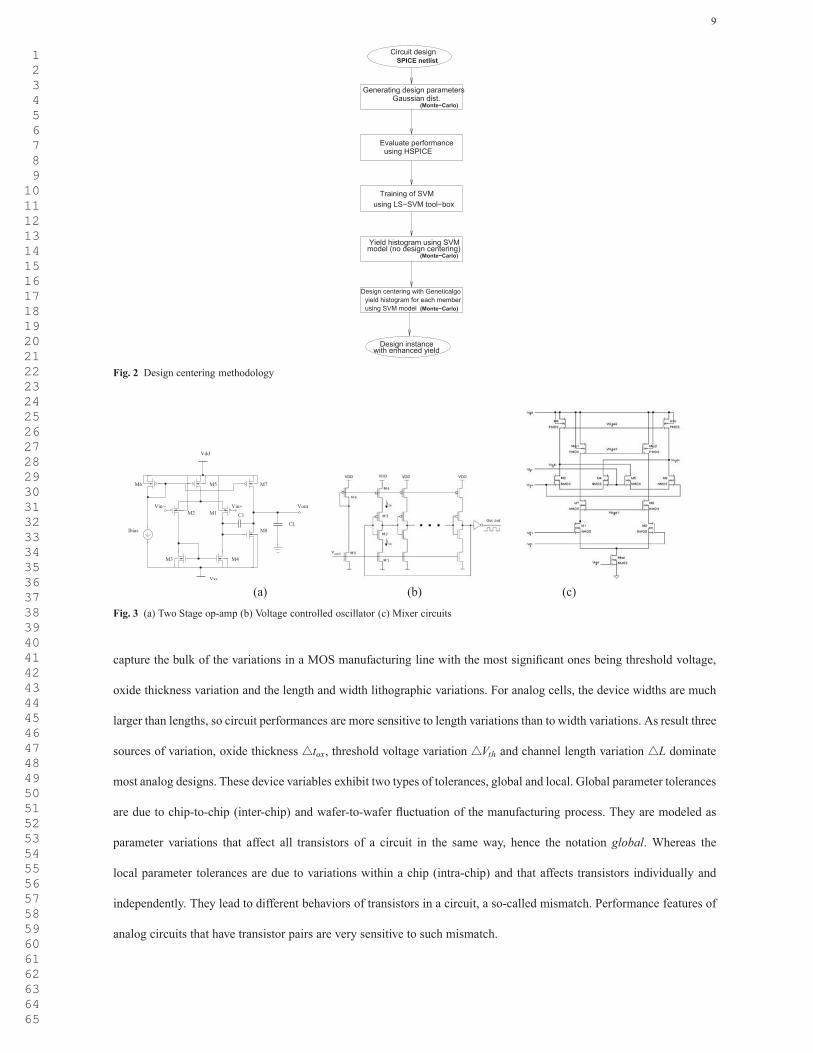
The overall methodology used for design centering is illustrated in 2.
5 Experimental Setup
The two-stage op amp, voltage-controlled-oscillator (VCO) and mixer circuit as shown in Figure 3, have been chosen to
illustrate design centering for sizing. Authors have shown in [22] that relatively few device variables have capability to
1 2 3 4 5 6 7 8 9 1011121314151617181920212223242526272829303132333435363738394041424344454647484950515253545556575859606162636465
9
Design instancewith enhanced yield
Gaussian dist.Generating design parameters
using HSPICEEvaluate performance
model (no design centering)(Monte−Carlo)
(Monte−Carlo)
(Monte−Carlo)
Training of SVMusing LS−SVM tool−box
Yield histogram using SVM
yield histogram for each memberusing SVM model
Design centering with Geneticalgo
SPICE netlistCircuit design
Fig. 2 Design centering methodology
CLIbias
M3 M4
M1M2
M5 M7M6
C1
Vdd
Vss
VoutVin− Vin+
M8
(a) (b) (c)
Fig. 3 (a) Two Stage op-amp (b) Voltage controlled oscillator (c) Mixer circuits
capture the bulk of the variations in a MOS manufacturing line with the most significant ones being threshold voltage,
oxide thickness variation and the length and width lithographic variations. For analog cells, the device widths are much
larger than lengths, so circuit performances are more sensitive to length variations than to width variations. As result three
sources of variation, oxide thickness �tox, threshold voltage variation �Vth and channel length variation �L dominate
most analog designs. These device variables exhibit two types of tolerances, global and local. Global parameter tolerances
are due to chip-to-chip (inter-chip) and wafer-to-wafer fluctuation of the manufacturing process. They are modeled as
parameter variations that affect all transistors of a circuit in the same way, hence the notation global. Whereas the
local parameter tolerances are due to variations within a chip (intra-chip) and that affects transistors individually and
independently. They lead to different behaviors of transistors in a circuit, a so-called mismatch. Performance features of
analog circuits that have transistor pairs are very sensitive to such mismatch.
1 2 3 4 5 6 7 8 9 1011121314151617181920212223242526272829303132333435363738394041424344454647484950515253545556575859606162636465
10
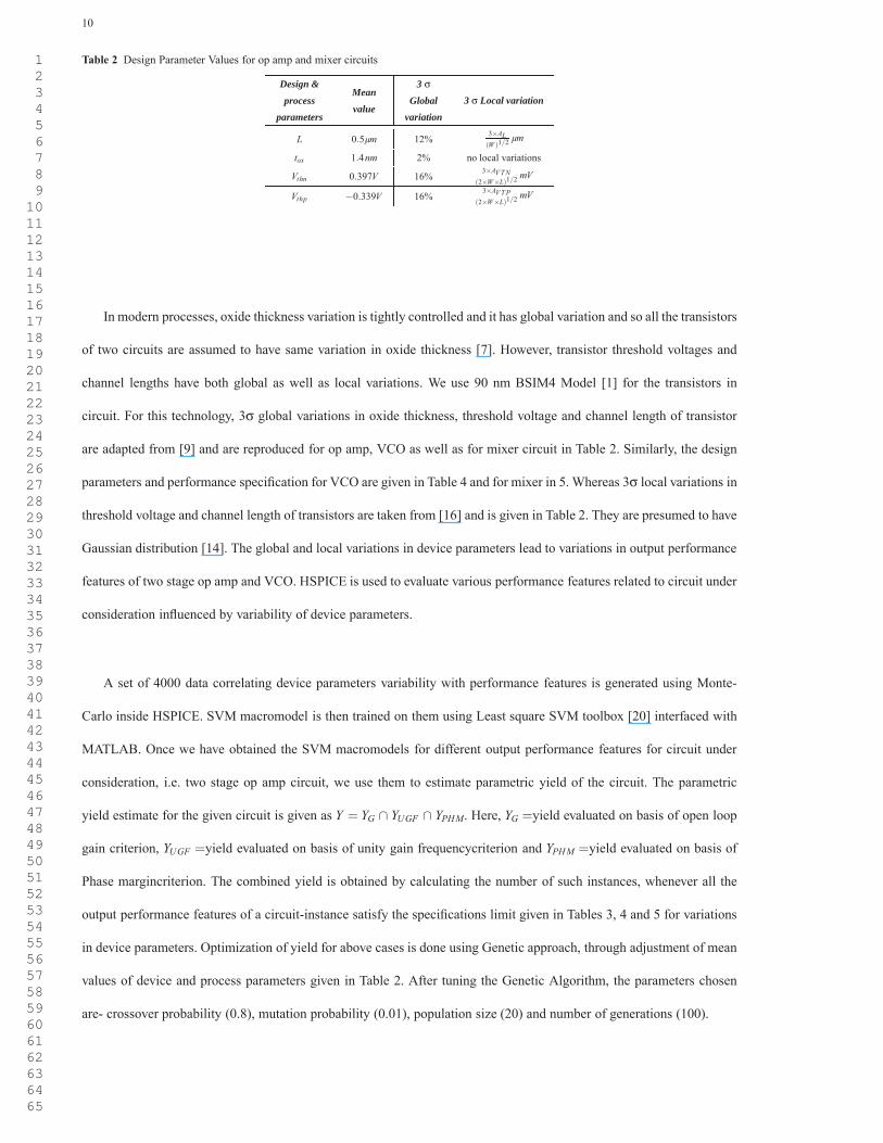
Table 2 Design Parameter Values for op amp and mixer circuits
Design &process
parameters
Meanvalue
3 σ
Globalvariation
3 σ Local variation
L 0.5μm 12% 3×AL(W )1/2
μm
tox 1.4nm 2% no local variations
Vthn 0.397V 16%3×AVTN
(2×W×L)1/2mV
Vthp −0.339V 16%3×AVTP
(2×W×L)1/2mV
In modern processes, oxide thickness variation is tightly controlled and it has global variation and so all the transistors
of two circuits are assumed to have same variation in oxide thickness [7]. However, transistor threshold voltages and
channel lengths have both global as well as local variations. We use 90 nm BSIM4 Model [1] for the transistors in
circuit. For this technology, 3σ global variations in oxide thickness, threshold voltage and channel length of transistor
are adapted from [9] and are reproduced for op amp, VCO as well as for mixer circuit in Table 2. Similarly, the design
parameters and performance specification for VCO are given in Table 4 and for mixer in 5. Whereas 3σ local variations in
threshold voltage and channel length of transistors are taken from [16] and is given in Table 2. They are presumed to have
Gaussian distribution [14]. The global and local variations in device parameters lead to variations in output performance
features of two stage op amp and VCO. HSPICE is used to evaluate various performance features related to circuit under
consideration influenced by variability of device parameters.
A set of 4000 data correlating device parameters variability with performance features is generated using Monte-
Carlo inside HSPICE. SVM macromodel is then trained on them using Least square SVM toolbox [20] interfaced with
MATLAB. Once we have obtained the SVM macromodels for different output performance features for circuit under
consideration, i.e. two stage op amp circuit, we use them to estimate parametric yield of the circuit. The parametric
yield estimate for the given circuit is given as Y = YG ∩ YUGF ∩ YPHM. Here, YG =yield evaluated on basis of open loop
gain criterion, YUGF =yield evaluated on basis of unity gain frequencycriterion and YPHM =yield evaluated on basis of
Phase margincriterion. The combined yield is obtained by calculating the number of such instances, whenever all the
output performance features of a circuit-instance satisfy the specifications limit given in Tables 3, 4 and 5 for variations
in device parameters. Optimization of yield for above cases is done using Genetic approach, through adjustment of mean
values of device and process parameters given in Table 2. After tuning the Genetic Algorithm, the parameters chosen
are- crossover probability (0.8), mutation probability (0.01), population size (20) and number of generations (100).
1 2 3 4 5 6 7 8 9 1011121314151617181920212223242526272829303132333435363738394041424344454647484950515253545556575859606162636465
11
45 50 55 600
200
400
600
800
1000
1200
Gain in dB
No
of s
ampl
es
5 6 7 8 9x 10⁷
0
200
400
600
800
1000
1200
UGF in HZ
Combined Yield=19.08%
20 40 60 80 1000
50
100
150
200
250
300
350
400
450
500
PHM in degree
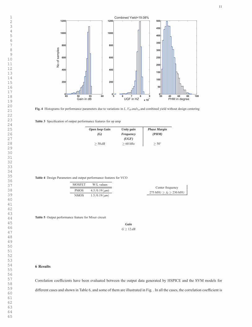
Fig. 4 Histograms for performance parameters due to variations in L,Vth and toxand combined yield without design centering
Table 3 Specification of output performance features for op amp
Open loop Gain(G)
Unity gainFrequency
(UGF)
Phase Margin(PHM)
≥ 50dB ≥ 60Mhz ≥ 50◦
Table 4 Design Parameters and output performance features for VCO
MOSFET W/L values
PMOS 4.5/0.19(μm)NMOS 1.5/0.19(μm)
Center frequency275MHz ≥ f0 ≥ 230MHz
Table 5 Output performance feature for Mixer circuit
GainG≥ 12dB
6 Results
Correlation coefficients have been evaluated between the output data generated by HSPICE and the SVM models for
different cases and shown in Table 6, and some of them are illustrated in Fig. . In all the cases, the correlation coefficient is
1 2 3 4 5 6 7 8 9 1011121314151617181920212223242526272829303132333435363738394041424344454647484950515253545556575859606162636465
12
51.6 51.8 52 52.2 52.40
100
200
300
400
500
600
Gain in dB
No
of s
ampl
es
6 6.2 6.4 6.6 6.8x 10⁷
0
100
200
300
400
500
600
700
UGF in Hz
Combined Yield=100%
50 55 60 65 700
100
200
300
400
500
600
PHM in degree
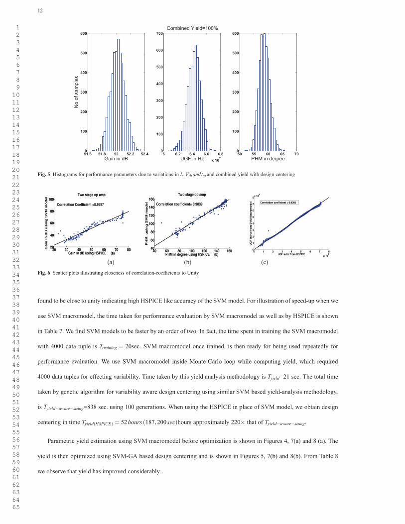
Fig. 5 Histograms for performance parameters due to variations in L, Vth and toxand combined yield with design centering
(a) (b) (c)
Fig. 6 Scatter plots illustrating closeness of correlation-coefficients to Unity
found to be close to unity indicating high HSPICE like accuracy of the SVMmodel. For illustration of speed-up when we
use SVM macromodel, the time taken for performance evaluation by SVM macromodel as well as by HSPICE is shown
in Table 7. We find SVM models to be faster by an order of two. In fact, the time spent in training the SVM macromodel
with 4000 data tuple is Ttraining = 20sec. SVM macromodel once trained, is then ready for being used repeatedly for
performance evaluation. We use SVM macromodel inside Monte-Carlo loop while computing yield, which required
4000 data tuples for effecting variability. Time taken by this yield analysis methodology is Tyield=21 sec. The total time
taken by genetic algorithm for variability aware design centering using similar SVM based yield-analysis methodology,
is Tyield−aware−sizing=838 sec. using 100 generations. When using the HSPICE in place of SVM model, we obtain design
centering in time Tyield(HSPICE) = 52hours (187,200sec)hours approximately 220× that of Tyield−aware−sizing.
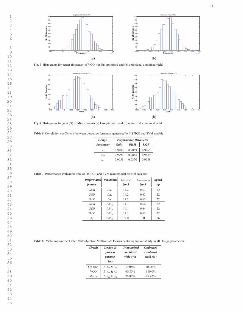
Parametric yield estimation using SVM macromodel before optimization is shown in Figures 4, 7(a) and 8 (a). The
yield is then optimized using SVM-GA based design centering and is shown in Figures 5, 7(b) and 8(b). From Table 8
we observe that yield has improved considerably.
1 2 3 4 5 6 7 8 9 1011121314151617181920212223242526272829303132333435363738394041424344454647484950515253545556575859606162636465
13
2.15 2.2 2.25 2.3 2.35 2.4x 10⁸
0
50
100
150
200
250
300
350
400
450
500
Frequency
No
Of S
ampl
es
Unoptimized Yield=60.80%
2.245 2.25 2.255 2.26 2.265 2.27 2.275 2.28 2.285 2.29x 10⁸
0
50
100
150
200
250
300
350
400
450
500
Frequency
No
Of S
ampl
es
Optimized Yield=100%
(a) (b)
Fig. 7 Histograms for center-frequency of VCO- (a) Un-optimized and (b) optimized, combined yield
11.96 11.98 12 12.02 12.04 12.06 12.08 12.1 12.12 12.140
50
100
150
200
250
300
350
Gain
No
Of S
ampl
es
Unoptimized Yield=76.82%
11.96 11.98 12 12.02 12.04 12.06 12.08 12.1 12.12 12.140
50
100
150
200
250
300
350
400
Gain
No
Of S
ampl
es
Optimized Yield=88.47%
(a) (b)
Fig. 8 Histograms for gain (G) of Mixer circuit- (a) Un-optimized and (b) optimized, combined yield
Table 6 Correlation coefficients between output performance generated by HSPICE and SVM models
Design Performance ParameterParameter Gain PHM UGF
L 0.9780 0.9839 0.9867Vth 0.9797 0.9865 0.9829tox 0.9951 0.9370 0.9988
Table 7 Performance evaluation time of HSPICE and SVM macromodel for 500 data sets
Performancefeature
Variations THSPICE(sec)
Tmacromodel(sec)
Speedup
Gain �L 14.2 0.63 22UGF �L 14.2 0.63 22PHM �L 14.2 0.63 22Gain �Vth 14.1 0.64 22UGF �Vth 14.1 0.64 22PHM �Vth 14.1 0.63 22f0 �Vth 79.0 3.0 26
Table 8 Yield improvement after Multiobjective Multivariate Design centering for variability in all Design parameters
Circuit Design &processparame-
ters
Unoptimizedcombinedyield (%)
Optimizedcombinedyield (%)
Op amp L, tox&Vth 19.08% 100.0 %VCO L, tox&Vth 60.80% 100.0%Mixer L, tox&Vth 76.82% 88.47%
1 2 3 4 5 6 7 8 9 1011121314151617181920212223242526272829303132333435363738394041424344454647484950515253545556575859606162636465
14
7 Conclusions
A process-aware SVM Model has been developed, which can link the process parameter variations to performance
parameters for analog circuits. Applicability of the model during sizing has been illustrated by performing yield analysis
with process variability using an example circuits i.e., two stage op-amp and VCO. The model has been found to be
highly efficient and is close in accuracy to SPICE. It has been found that Monte Carlo analysis using SVM model based
evaluation is much faster than SPICE based evaluation with almost similar accuracy. The effects of variation in channel
length and threshold voltage on the yield were observed to be significant. The process of design centered sizing has been
illustrated using Genetic Algorithm. Yield has been improved considerably and thus the impact of process variations has
been minimized during sizing for two-stage op-amp and VCO circuits using 90 nm technology.
References
1. BSIM Homepage - Offical Site, http://www-device.eecs.berkeley.edu/ bsim3/bsim4
2. Barros, M., Guiherme, J., Horta, N.: GA-SVM feasibility model and optimization kernel applied to analog ICs design automation. In:
Proc. 17th ACM Great Lake Symposium on VLSI, USA, pp. 469–472 (2007)
3. Boolchandani, D., Ahmed, A., Sahula, V.: Efficient kernel functions for support vector machine regression model for analog circuits’
performance evaluation. Analog Integrated Circuits and Signal Processing 66, 117–128 (2011). URL http://dx.doi.org/10.1007/s10470-
010-9476-6. DOI-10.1007/s10470-010-9476-6
4. Boughorbel, S., Tarel, J.P., Boujemaa, N.: Conditionally positive definite kernels for svm based image recognition. In: Proceedings of
ICME, pp. 113–116 (2005)
5. Ding, M., Vemuri, R.: A combined feasibility and performance macromodel for analog circuits. In: Proceedings of IEEE Design Automa-
tion Conference, pp. 63–68 (2005)
6. Goldberg, D.E.: "Genetic Algorithms in Search, Optimization and Machine Learning". Addison-Wesley Longman Publishing Co., Inc.
(1989)
7. Graeb, H.E.: Analog design centering and sizing. Springer Publishing Co. (2007)
8. Hershenson, M., Boyd, S., Lee, T.: Optimal design of a CMOS op-amp via geometric programming. IEEE Transactions on Computer-
Aided Design of Integrated Circuits and Systems 20(1), 1–21 (2001)
9. ITRS: International Techology Roadmap for Semiconductors. Tech. rep. (2009)
10. Kiely, T., Gielen, G.G.E.: Performance modeling of analog integrated circuits using least-squares support vector machines. In: Proceedings
of DATE, pp. 448–453 (2004)
11. Kurker, C., Paulos, J., Gyurcsik, R., Lu, J.C.: Hierarchical yield estimation of large analog integrated circuits. In: IEEE Journal of Solid-
State Circuits, vol. 28, pp. 203–209 (1993)
12. Li, X., Pileggi, L.: Efficient parametric yield extraction for multiple correlated non-normal performance distributions of analog/RF circuits.
In: Proc. IEEE ACM Design automation Conference, USA (2007)
1 2 3 4 5 6 7 8 9 1011121314151617181920212223242526272829303132333435363738394041424344454647484950515253545556575859606162636465

15
13. McConaghy, T., Gielen, G.: Globally reliable variation-aware sizing of analog integrated circuits via response surfaces and structural
homotopy. IEEE Trans. on CAD of ICs and Systems 28(11), 1627–1640 (2009)
14. Pelgrom, M., Duinmaijer, A.,Welbers, A.: Matching properties of MOS transistors. IEEE Journal of Solid-State Circuits, 24(5), 1433–1439
(1989)
15. Pratap, R., Sen, P., Davis, C., Mukhophdhyay, R., May, G., Laskar, J.: Neurogenetic design centering. In: IEEE Transactions on Semicon-
ductor Manufacturing, vol. 19, pp. 173–182 (2006)
16. Sansen, W.M.: Analog Design Essentials. Springer (2006)
17. Schenkel, F., Pronath, M., Zizala, S., Schwencker, R., Graeb, H., Antreich, K.: Mismatch analysis and direct yield optimization by spec-
wise linearization and feasibility-guided search. In: Design Automation Conference, 2001. Proceedings, pp. 858 – 863 (2001)
18. S.K.Tiwary, P.K.Tiwary, Rutenbar, R.A.: Generation of yield-aware pareto surfaces for hierarchical circuit design space exploration. In:
Proceedings of IEEE Design Automation Conference, pp. 31–36 (2006)
19. Smits, G., Jordaan, E.: Improved SVM regression using mixtures of kernels. In: Proceedings of International Joint Conference on Neural
Networks, vol. 3, pp. 2785–2790 (2002)
20. Suykens, J.A.: Least squares support vector machine matlab/c toolbox. http://www.esat.kuleuven.be/sista/lssvmlab (2003)
21. Suykens, J.A., Gestel, T., Brabenter, J., Moor, B., Vandewalle, J.: Least Square Support vector Machines. World Scientific Publishing Co.
Pte. Ltd (2002)
22. T. Mukherjee, L., Rutenbar, R.: Efficient handling of operating range and manufacturing line variations in analog cell synthesis. In: IEEE
Trans. Computer-Aided Design, vol. 19 (2000)
23. Vapnik, V.: The Nature of Statistical Learning Theory. Springer-Verlag, NY USA (1995)
1 2 3 4 5 6 7 8 9 1011121314151617181920212223242526272829303132333435363738394041424344454647484950515253545556575859606162636465

D. Boolchandani obtained his Bachelor of Engineering degree in Electronics with honors from erstwhile Regional Engineering College now Malaviya National Institute of Technology, Jaipur in 1988. He obtained a Master of Technology degree in Design & Technology from the Indian Institute of Science in 1998. He is currently Associate Professor the Department of Electronics and Communications Engineering at National Institute of TEchnology Jaipur, India. He is currently working towards his doctorate thesis entitled Analog Macromodeling. His research interests are in the area analog & digital CMOS circuits and Analog CAD. He is a member of IEEE, and member of IETE India
*Author BiographiesClick here to download Author Biographies: dbool-bio.txt

Lokesh garg obtained his Bachelor of Engineering degree in Electronics & Communication from Seedling Academy of Design, tech. & Management, Jaipur in 2007 . He obtained a Master of Technology degree in VLSI Design from the Malviya National Institute of Technology, Jaipur in 2010. He is currently pursuing his Ph.D in field of VLSI at Electronics and Communications Engineering Department in Malviya National Institute of Technology Jaipur, India. His research interests are in the area of optimization of analog & digital CMOS circuits and Analog CAD.
*Author BiographiesClick here to download Author Biographies: lokesh-bio.txt

Sapna Khandelwal obtained his Bachelor of Engineering degree in Electronics & Communication from Shri Balaji college of Engg. & Technology, Jaipur in 2004 . He obtained a Master of Technology degree in VLSI Design from the Malviya National Institute of Technology, Jaipur in 2010. She is currently Assistant Professor in Kautilya college of Tech & Engg. Jaipur, India. Her research interests are in the area of optimization of analog & digital CMOS circuits and Analog CAD.
*Author BiographiesClick here to download Author Biographies: sapna.txt

Vineet Sahula obtained his Bachelor of Engineering degree in Electronics with honors from erstwhile Regional Engineering College now Malaviya National Institute of Technology, Jaipur in 1987. He obtained a Master of Technology degree in Integrated Electronics & Circuits from the Indian Institute of Technology, Delhi in 1989. He is currently Associate Professor the Department of Electronics and Communications Engineering at National Institute of TEchnology Jaipur, India. He earned Ph.D. from Department of Electrical engineering, Indian Institute of Technology, Delhi in 2001. His research interests are in the areas related to high level design, modeling and synthesis foo analog & digital systems, and CAD for VLSI. He has two journal papers and more than 30 refereed conferences papers to his credit. He has served on the Technical programme committee of the VLSI Design and Test Symposium held in India (1998-2009). He has also served on organizing committee as fellowship-chair of 22nd IEEE International Conference on VLSI Design, 2009 India. He is a senior member of IEEE, Life Fellow of IETE, Life member of IMAPS and member of VLSI Society of India and ACM SIGDA.
*Author BiographiesClick here to download Author Biographies: vineet-bio.txt
*Author PhotographsClick here to download high resolution image
*Author PhotographsClick here to download high resolution image

*Author PhotographsClick here to download high resolution image

*Author PhotographsClick here to download high resolution image